Embed Size (px)
Citation preview
Wireless Power Receiver
for 15W Applications
P9221-R Datasheet
© 2017 Integrated Device Technology, Inc. 1 October 10, 2017
AC1
COMM1
BST1
AC2
COMM2
BST2 VR
EC
T
OUT
VO
SE
T/Q
-Fac
t
TS
/EO
C
RP
PO
RP
PG
SDA
SCL
INT
VD
D5V
GN
D
Programming
Resistors
LS
P9221-R
ILIM
ALI
GN
X
ALI
GN
Y
VD
D18
CS
COUT
Description
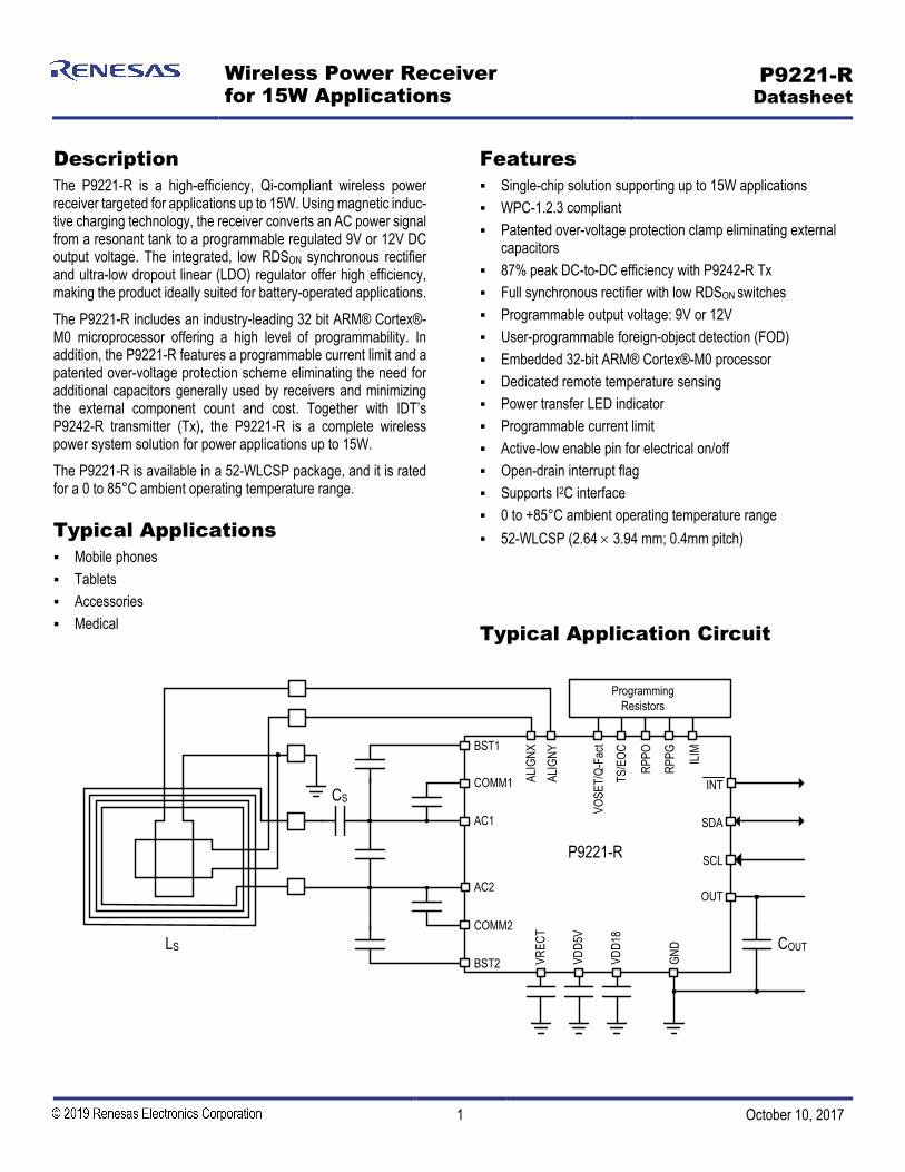
The P9221-R is a high-efficiency, Qi-compliant wireless power receiver targeted for applications up to 15W. Using magnetic induc-tive charging technology, the receiver converts an AC power signal from a resonant tank to a programmable regulated 9V or 12V DC output voltage. The integrated, low RDSON synchronous rectifier and ultra-low dropout linear (LDO) regulator offer high efficiency, making the product ideally suited for battery-operated applications.
The P9221-R includes an industry-leading 32 bit ARM® Cortex®-M0 microprocessor offering a high level of programmability. In addition, the P9221-R features a programmable current limit and a patented over-voltage protection scheme eliminating the need for additional capacitors generally used by receivers and minimizing the external component count and cost. Together with IDT’s P9242-R transmitter (Tx), the P9221-R is a complete wireless power system solution for power applications up to 15W.
The P9221-R is available in a 52-WLCSP package, and it is rated for a 0 to 85°C ambient operating temperature range.
Typical Applications
Mobile phones
Tablets
Accessories
Medical
Features
Single-chip solution supporting up to 15W applications
WPC-1.2.3 compliant
Patented over-voltage protection clamp eliminating external capacitors
87% peak DC-to-DC efficiency with P9242-R Tx
Full synchronous rectifier with low RDSON switches
Programmable output voltage: 9V or 12V
User-programmable foreign-object detection (FOD)
Embedded 32-bit ARM® Cortex®-M0 processor
Dedicated remote temperature sensing
Power transfer LED indicator
Programmable current limit
Active-low enable pin for electrical on/off
Open-drain interrupt flag
Supports I2C interface
0 to +85°C ambient operating temperature range
52-WLCSP (2.64 3.94 mm; 0.4mm pitch)
Typical Application Circuit
P9221-R Datasheet
© 2017 Integrated Device Technology, Inc. 2 October 10, 2017
Contents
1. Pin Assignments ...........................................................................................................................................................................................5
2. Pin Descriptions ............................................................................................................................................................................................6
3. Absolute Maximum Ratings ..........................................................................................................................................................................8
4. Thermal Characteristics ................................................................................................................................................................................9
5. Electrical Characteristics ..............................................................................................................................................................................9
6. Typical Performance Characteristics ..........................................................................................................................................................12
7. Functional Block Diagram ...........................................................................................................................................................................15
8. Theory of Operation ....................................................................................................................................................................................16
8.1 LDO – Low Dropout Regulators .......................................................................................................................................................16
8.2 Setting the Output Voltage and Reference Q-factor Value – VOSET/Q-Fact Pin ............................................................................16
8.3 SINK Pin ..........................................................................................................................................................................................17
8.4 Rectifier Voltage – VRECT ...............................................................................................................................................................17
8.5 Over-Current Limit – ILIM .................................................................................................................................................................17
8.6 Interrupt Function – INT ...................................................................................................................................................................18
8.7 Enable Pin – EN ...............................................................................................................................................................................18
8.8 Thermal Protection ...........................................................................................................................................................................18
8.9 External Temperature Sensing and End of Charge – TS/EOC ........................................................................................................18
8.10 Alignment Guide – ALIGNX and ALIGNY ........................................................................................................................................18
8.11 Advanced Foreign Object Detection (FOD) .....................................................................................................................................19
8.12 Received Power Packet Offset and Gain Calibration – RPPO and RPPG ......................................................................................20
9. Communication Interface ............................................................................................................................................................................21
9.1 Modulation/Communication ..............................................................................................................................................................21
9.2 Bit Encoding Scheme for ASK .........................................................................................................................................................22
9.3 Byte Encoding for ASK.....................................................................................................................................................................22
9.4 Packet Structure ..............................................................................................................................................................................22
10. WPC Mode Characteristics ........................................................................................................................................................................23
10.1 Selection Phase or Startup ..............................................................................................................................................................23
10.2 Ping Phase (Digital Ping) .................................................................................................................................................................23
10.3 Identification and Configuration Phase ............................................................................................................................................24
10.4 Negotiation Phase ............................................................................................................................................................................24
10.5 Calibration Phase .............................................................................................................................................................................24
10.6 Power Transfer Phase .....................................................................................................................................................................24
11. Functional Registers ...................................................................................................................................................................................25
12. Application Information ...............................................................................................................................................................................29
12.1 Power Dissipation and Thermal Requirements ................................................................................................................................29
12.2 Recommended Coils ........................................................................................................................................................................30
12.3 Typical Application Schematic .........................................................................................................................................................31
12.4 Bill of Materials (BOM) .....................................................................................................................................................................32
P9221-R Datasheet
© 2017 Integrated Device Technology, Inc. 3 October 10, 2017
13. Package Drawings ......................................................................................................................................................................................34
14. Recommended Land Pattern ......................................................................................................................................................................35
15. Special Notes: WLCSP-52 (AHG52) Package Assembly ...........................................................................................................................36
16. Marking Diagram ........................................................................................................................................................................................36
17. Ordering Information ...................................................................................................................................................................................36
18. Revision History ..........................................................................................................................................................................................37
List of Figures
Figure 1. Pin Assignments ..................................................................................................................................................................................5
Figure 2. Efficiency vs. Output Load: VOUT = 12V .............................................................................................................................................12
Figure 3. Load Reg. vs. Output Load: VOUT = 12V ............................................................................................................................................12
Figure 4. Efficiency vs. Output Load: VOUT = 9V ...............................................................................................................................................12
Figure 5. Load Reg. vs. Output Load: VOUT = 9V ..............................................................................................................................................12
Figure 6. Efficiency vs. Output Load: VOUT = 5V ...............................................................................................................................................12
Figure 7. Load Reg. vs. Output Load: VOUT = 5V ..............................................................................................................................................12
Figure 8. Rectifier Voltage vs. Load: VOUT = 12V ..............................................................................................................................................13
Figure 9. Rectifier Voltage vs. Load: VOUT = 9V ................................................................................................................................................13
Figure 10. Rectifier Voltage vs. Load: VOUT = 5V ................................................................................................................................................13
Figure 11. Current Limit vs. VILIM ........................................................................................................................................................................13
Figure 12. X and Y Misalignment ........................................................................................................................................................................13
Figure 13. Max. Power vs. Misalignment: VOUT=12V ..........................................................................................................................................13
Figure 14. Enable Startup: VOUT = 12V; IOUT = 1.2A ............................................................................................................................................14
Figure 15. Transient Resp: VOUT = 12V; IOUT = 0 to 1.2A ....................................................................................................................................14
Figure 16. Transient Resp: VOUT = 12V; IOUT = 1.3A to 0 ....................................................................................................................................14
Figure 17. Functional Block Diagram ..................................................................................................................................................................15
Figure 18. Example of Differential Bi-phase Decoding for FSK ..........................................................................................................................21
Figure 19. Example of Asynchronous Serial Byte Format for FSK .....................................................................................................................21
Figure 20. Bit Encoding Scheme ........................................................................................................................................................................22
Figure 21. Byte Encoding Scheme .....................................................................................................................................................................22
Figure 22. Communication Packet Structure ......................................................................................................................................................22
Figure 23. WPC Power Transfer Phases Flowchart ...........................................................................................................................................23
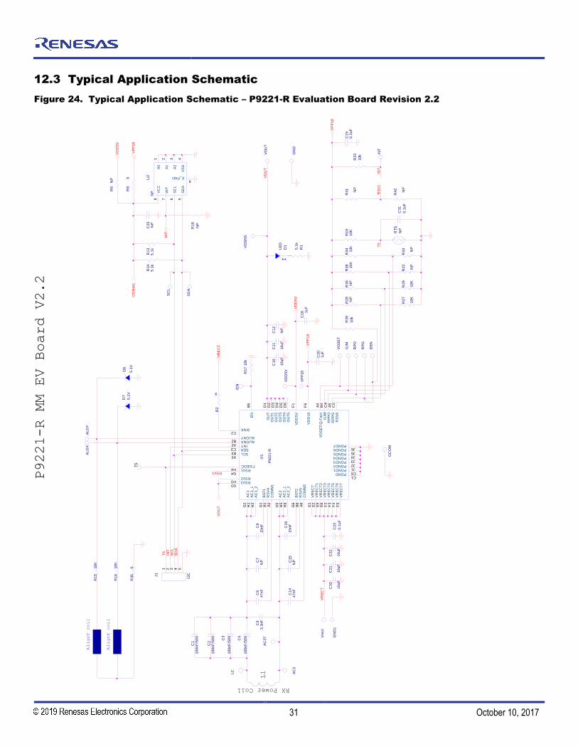
Figure 24. Typical Application Schematic – P9221-R Evaluation Board Revision 2.2 ........................................................................................31
Figure 25. Package Outline Drawing (AHG52) ...................................................................................................................................................34
Figure 26. 52-WLCSP (AHG52) Land Pattern ....................................................................................................................................................35
P9221-R Datasheet
© 2017 Integrated Device Technology, Inc. 4 October 10, 2017
List of Tables
Table 1. Pin Descriptions ...................................................................................................................................................................................6
Table 2. Absolute Maximum Ratings .................................................................................................................................................................8
Table 3. ESD Information ..................................................................................................................................................................................8
Table 4. Package Thermal Information .............................................................................................................................................................9
Table 5. Electrical Characteristics .....................................................................................................................................................................9
Table 6. Setting the Output Voltage and Reference Q-factor Value ................................................................................................................17
Table 7. Setting the Over Current Limit ...............................................................................................................................................................17
Table 8. Maximum Estimated Power Loss ......................................................................................................................................................19
Table 9. Device Identification Register ............................................................................................................................................................25
Table 10. Firmware Major Revision ...................................................................................................................................................................25
Table 11. Firmware Minor Revision ...................................................................................................................................................................25
Table 12. Status Registers ................................................................................................................................................................................25
Table 13. Interrupt Status Registers ..................................................................................................................................................................26
Table 14. Interrupt Enable Registers .................................................................................................................................................................26
Table 15. Battery Charge Status .......................................................................................................................................................................27
Table 16. End Power Transfer ...........................................................................................................................................................................27
Table 17. Read Register – Output Voltage ........................................................................................................................................................27
Table 18. Read Register – VRECT Voltage ......................................................................................................................................................27
Table 19. Read Register – IOUT Current ..........................................................................................................................................................27
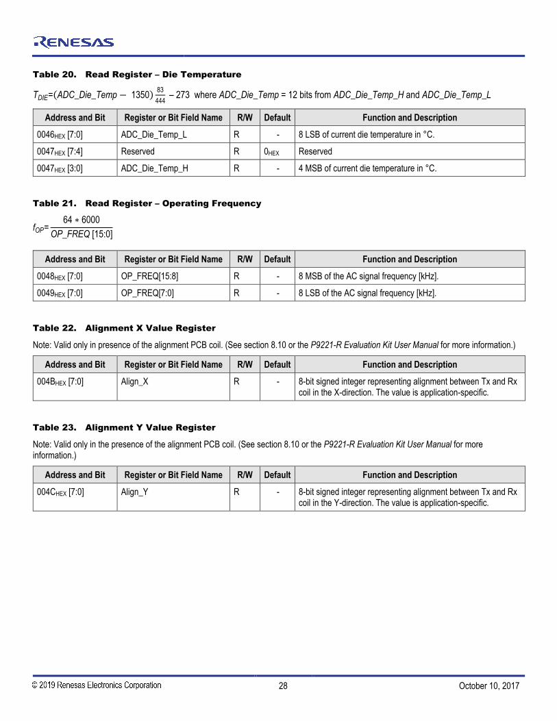
Table 20. Read Register – Die Temperature .....................................................................................................................................................28
Table 21. Read Register – Operating Frequency ..............................................................................................................................................28
Table 22. Alignment X Value Register ...............................................................................................................................................................28
Table 23. Alignment Y Value Register ...............................................................................................................................................................28
Table 24. Command Register ............................................................................................................................................................................29
Table 25. Recommended Coil Manufacturers ...................................................................................................................................................30
Table 26. P9221-R MM Evaluation Kit V2.2 Bill of Materials .............................................................................................................................32
P9221-R Datasheet
© 2017 Integrated Device Technology, Inc. 5 October 10, 2017
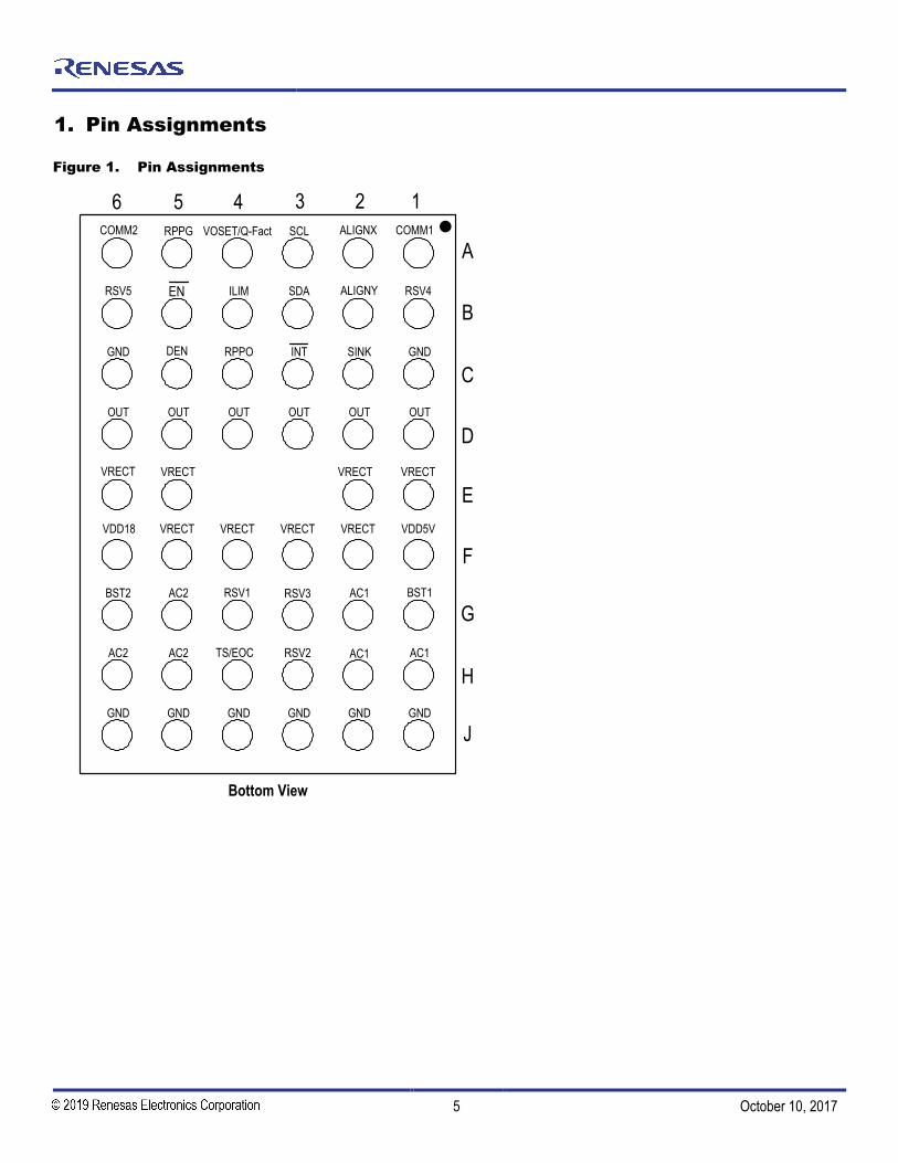
1. Pin Assignments
Figure 1. Pin Assignments
COMM1
RSV4
GND
OUT
ALIGNX
ALIGNY
SINK
OUT
SCL
SDA
INT
OUT
ILIM
RPPO
OUT
RPPG
DEN
OUT
COMM2
RSV5
GND
OUT
A
B
C
D
E
F
123456
AC1RSV3
TS/EOC
AC2BST2
GBST1
AC1RSV2
RSV1
AC2AC2
H
AC1
GNDGNDGNDGNDGNDGND
J
Bottom View
EN
VDD18 VDD5VVRECT VRECT VRECT VRECT
VRECT VRECTVRECTVRECT
VOSET/Q-Fact

P9221-R Datasheet
© 2017 Integrated Device Technology, Inc. 6 October 10, 2017
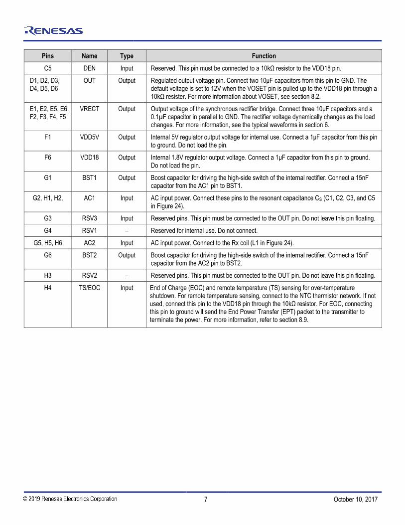
2. Pin Descriptions
Table 1. Pin Descriptions
Pins Name Type Function
A1 COMM1 Output Open-drain output used to communicate with the transmitter. Connect a 47nF capacitor from AC1 to COMM1.
A2 ALIGNX Input AC input for coil alignment guide. If not used, connect this pin to GND through a 10kΩ resistor.
A3 SCL Input Serial clock line. Open-drain pin. Connect this pin to a 5.1kΩ resistor to the VDD18 pin.
A4 VOSET/ Q-Fact
Input Programming pin for setting the output voltage and Q-factor. For VOSET, connect this pin to the center tap of a resistor divider to set the output voltage. For more information, refer to section 8.2 for different output voltage settings and section 8.2 for adjusting the Q-factor value.
A5 RPPG Input Received power packet gain (RPPG) calibration pin for foreign object detection (FOD) tuning. Connect this pin to the center tap of a resistor divider to set the gain of the FOD. The FOD is disabled by connecting the RPPG and RPPO pins to GND. Do not leave this pin floating.
A6 COMM2 Output Open-drain output used to communicate with the transmitter. Connect a 47nF capacitor from AC2 to COMM2.
B1 RSV4 – Reserved for internal use. Do not connect.
B2 ALIGNY Input AC input for coil alignment guide. If not used, connect to GND through a 10kΩ resistor.
B3 SDA Input/Output Serial data line. Open-drain pin. Connect a 5.1kΩ resistor to VDD18 pin.
B4 ILIM Input Programmable over-current limit pin. Connect this pin to the center tap of a resistor divider to set the current limit. For more information about the current limit function, see section 8.5.
B5 EN Input Active-LOW enable pin. Pulling this pin to logic HIGH forces the device into Shut Down Mode. When connected to logic LOW, the device is enabled. Do not leave this pin floating.
B6 RSV5 – Reserved for internal use. Do not connect.
C1, C6, J1, J2, J3, J4, J5, J6
GND GND Ground.
C2 SINK Output Open-drain output for controlling the rectifier clamp. Connect a 36Ω resistor from this pin to the VRECT pin.
C3 INT Output Interrupt flag pin. This is an open-drain output that signals fault interrupts. It is pulled LOW if any of these faults exist: an over-voltage is detected, an over-current condition is detected, the die temperature exceeds 140°C, or an external over-temperature condition is detected on the TS pin.
It is also asserted LOW when EN is HIGH. Connect INT to VDD18 through a 10kΩ resistor. See section 8.6 for additional conditions affecting the interrupt flag.
C4 RPPO Input Received power packet offset (RPPO) calibration pin for FOD tuning. Connect this pin to the center tap of the resistor divider to set the offset of the FOD. The FOD is disabled by connecting the RPPG and RPPO pins to GND. Do not leave this pin floating.
P9221-R Datasheet
© 2017 Integrated Device Technology, Inc. 7 October 10, 2017
Pins Name Type Function
C5 DEN Input Reserved. This pin must be connected to a 10kΩ resistor to the VDD18 pin.
D1, D2, D3, D4, D5, D6
OUT Output Regulated output voltage pin. Connect two 10μF capacitors from this pin to GND. The default voltage is set to 12V when the VOSET pin is pulled up to the VDD18 pin through a 10kΩ resister. For more information about VOSET, see section 8.2.
E1, E2, E5, E6, F2, F3, F4, F5
VRECT Output Output voltage of the synchronous rectifier bridge. Connect three 10μF capacitors and a 0.1µF capacitor in parallel to GND. The rectifier voltage dynamically changes as the load changes. For more information, see the typical waveforms in section 6.
F1 VDD5V Output Internal 5V regulator output voltage for internal use. Connect a 1μF capacitor from this pin to ground. Do not load the pin.
F6 VDD18 Output Internal 1.8V regulator output voltage. Connect a 1μF capacitor from this pin to ground. Do not load the pin.
G1 BST1 Output Boost capacitor for driving the high-side switch of the internal rectifier. Connect a 15nF capacitor from the AC1 pin to BST1.
G2, H1, H2, AC1 Input AC input power. Connect these pins to the resonant capacitance CS (C1, C2, C3, and C5 in Figure 24).
G3 RSV3 Input Reserved pins. This pin must be connected to the OUT pin. Do not leave this pin floating.
G4 RSV1 – Reserved for internal use. Do not connect.
G5, H5, H6 AC2 Input AC input power. Connect to the Rx coil (L1 in Figure 24).
G6 BST2 Output Boost capacitor for driving the high-side switch of the internal rectifier. Connect a 15nF capacitor from the AC2 pin to BST2.
H3 RSV2 – Reserved pins. This pin must be connected to the OUT pin. Do not leave this pin floating.
H4 TS/EOC Input End of Charge (EOC) and remote temperature (TS) sensing for over-temperature shutdown. For remote temperature sensing, connect to the NTC thermistor network. If not used, connect this pin to the VDD18 pin through the 10kΩ resistor. For EOC, connecting this pin to ground will send the End Power Transfer (EPT) packet to the transmitter to terminate the power. For more information, refer to section 8.9.

P9221-R Datasheet
© 2017 Integrated Device Technology, Inc. 8 October 10, 2017
3. Absolute Maximum Ratings
Stresses greater than those listed as absolute maximum ratings in Table 2 could cause permanent damage to the device. These are stress ratings only, and functional operation of the device at these or any other conditions above those indicated in the operational sections of this specification is not implied. Exposure to absolute maximum rating conditions for extended periods might affect reliability.
Table 2. Absolute Maximum Ratings
Pins [a],[b] Parameter Conditions Minimum [c] Maximum [c] Units
AC1 [d], AC2 [d], COMM1, COMM2 Absolute Maximum Pin Voltage -0.3 20 V
EN Absolute Maximum Pin Voltage -0.3 28 V
SINK, VRECT Absolute Maximum Pin Voltage -0.3 24 V
DEN, ILIM, RPPG, RPPO, VDD18, VOSET
Absolute Maximum Pin Voltage -0.3 2 V
ALIGNX, ALIGNY, INT , SCL, SDA, TS, VDD5V
Absolute Maximum Pin Voltage -0.3 6 V
BST1 Absolute Maximum Pin Voltage -0.3 AC1 + 6 V
BST2 Absolute Maximum Pin Voltage -0.3 AC2 + 6 V
OUT Absolute Maximum Pin Voltage -0.3 14.4 V
SINK Maximum Current on Pin – 1 A
COMM1, COMM2 Maximum RMS Current on Pin – 500 mA
AC1, AC2 Maximum RMS Current from Pin – 2 A
[a] Absolute maximum ratings are not provided for reserved pins (RSV1, RSV2, RSV3, RSV4, RSV5, and DEN). These pins are not used in the application.
[b] For the test conditions for the absolute maximum ratings specifications, the P9221-R characterization for the operating ambient temperature (TAMB) specification (see Table 4) has been performed down to -10°C only. Design simulation indicates normal operation down to -45°C. Limited bench functionality tests indicate normal operation down to -40°C.
[c] All voltages are referred to ground unless otherwise noted.
[d] During synchronous rectifier dead time, the voltage on the AC1 and AC2 pins is developed by current across the internal power FET’s body diodes, and it might be lower than -0.3 V. This is a normal behavior and does not negatively impact the functionality or reliability of the product.
Table 3. ESD Information
Test Model Pins Ratings Units
HBM All pins except RSV1, RSV2, RSV3, RSV4, and RSV5 pins 2 kV
RSV1, RSV2, RSV3, RSV4, and RSV5 pins 1 kV
CDM All pins 500 V

P9221-R Datasheet
© 2017 Integrated Device Technology, Inc. 9 October 10, 2017
4. Thermal Characteristics
Table 4. Package Thermal Information
Note: This thermal rating was calculated on a JEDEC 51 standard 4-layer board with dimensions 76.2 x 114.3 mm in still air conditions.
Symbol Description WLCSP Rating 8 Thermal Balls Units
θJA Thermal Resistance Junction to Ambient [a] 47 C/W
θJC Thermal Resistance Junction to Case 0.202 C/W
θJB Thermal Resistance Junction to Board 4.36 C/W
TJ Operating Junction Temperature[a] -5 to +125 C
TAMB Ambient Operating Temperature [a] 0 to +85 C
TSTOR Storage Temperature -55 to +150 C
TBUMP Maximum Soldering Temperature (Reflow, Pb-Free) 260 C
[a] The maximum power dissipation is PD(MAX) = (TJ(MAX) - TAMB) / θJA where TJ(MAX) is 125°C. Exceeding the maximum allowable power dissipation will result in excessive die temperature, and the device will enter thermal shutdown.
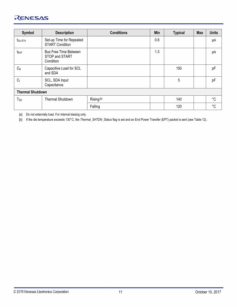
5. Electrical Characteristics
Table 5. Electrical Characteristics
Note: VRECT = 5.5V; COUT = 4.7μF, EN = LOW, unless otherwise noted. TJ = 0C to 125C; typical values are at 25°C.
Note: See important notes at the end of this table.
Symbol Description Conditions Min Typical Max Units
Under-Voltage Lock-Out (UVLO)
VUVLO_Rising UVLO Rising Rising voltage on VRECT 2.9 2.98 V
VUVLO_HYS UVLO Hysteresis VRECT falling 200 mV
Over-Voltage Protection
VOVP-DC DC Over-Voltage Protection
Rising voltage on VRECT 17 V
VOVP-HYS Over-Voltage Hysteresis 1 V
Quiescent Current
IACTIVE_SUPLY Supply Current EN¯¯ = Low, No load; VRECT = 12.3V 3.0 mA
ISHD Shut Down Mode Current EN¯¯ = High; VRECT = 12.3V 500 μA
VDD18 Voltage
VVDD18 VDD18 Pin Output Voltage [a]
IVDD18 = 10mA, CVDD18 = 1µF 1.62 1.8 1.98 V

P9221-R Datasheet
© 2017 Integrated Device Technology, Inc. 10 October 10, 2017
Symbol Description Conditions Min Typical Max Units
VDD5V Voltage
VVDD5V VDD5V Pin Output Voltage [a]
IVDD5V = 10mA, CVDD5V = 1µF 4.5 5 5.5 V
Low Drop-Out (LDO) Regulator
IOUT_MAX Maximum Output Current 1.25 A
VOUT_12V 12V Output Voltage VOSET > 1.5V, VRECT=12.3V 12 V
VOUT_9V 9V Output Voltage 0.7V < VOSET < 1.2V, VRECT=9.3V 9 V
Analog to Digital Converter
N Resolution 12 Bit
fSAMPLE Sampling Rate 67.5 kSa/s
Channel Number of Channels 8
VIN,FS Full-Scale Input Voltage 2.1 V
EN pin
VIH_EN¯¯ Input Threshold HIGH 1.4 V
VIL_EN¯¯ Input Threshold LOW 0.25 V
IIL_EN¯¯ Input Current LOW VEN¯¯ = 0V -1 1 μA
IIH_EN¯¯ Input Current HIGH VEN¯¯ = 5V 2.5 μA
VOSET, ILIM, TS, RPPO, RPPG
IIL Input Current LOW VVOSET, VILIM, VTS, VRPPO, VRPPG = 0V -1 1 µA
IIH Input Current HIGH VVOSET, VILIM, VTS, VRPPO, VRPPG = 1.8V -1 1 µA
ALIGNX, ALIGNY and INT pins
ILKG Input Leakage Current VALIGNX, VALIGNY, VINT = 0V and 5V -1 1 µA
VOL Output Logic LOW IOL = 8mA 0.36 V
I2C Interface – SCL, SDA
VIL Input Threshold LOW 0.7 V
VIH Input Threshold HIGH 1.4 V
ILKG Input Leakage Current VSCL, VSDA = 0V and 5V -1 1 µA
VOL Output Logic LOW IOL = 8mA 0.36 V
fSCL Clock Frequency 400 kHz
tHD,STA Hold Time (Repeated) for START Condition
0.6 µs
tHD:DAT Data Hold Time 0 ns
tLOW Clock Low Period 1.3 µs
tHIGH Clock High Period 0.6 µs
P9221-R Datasheet
© 2017 Integrated Device Technology, Inc. 11 October 10, 2017
Symbol Description Conditions Min Typical Max Units
tSU:STA Set-up Time for Repeated START Condition
0.6 µs
tBUF Bus Free Time Between STOP and START Condition
1.3 µs
CB Capacitive Load for SCL and SDA
150 pF
CI SCL, SDA Input Capacitance
5 pF
Thermal Shutdown
TSD Thermal Shutdown Rising [b] 140 °C
Falling 120 °C
[a] Do not externally load. For internal biasing only.
[b] If the die temperature exceeds 130°C, the Thermal_SHTDN_Status flag is set and an End Power Transfer (EPT) packet is sent (see Table 12).

P9221-R Datasheet
© 2017 Integrated Device Technology, Inc. 12 October 10, 2017
6. Typical Performance Characteristics
The following performance characteristics were taken using a P9242-R, 15W wireless power transmitter at TAMB = 25°C unless otherwise noted.
Figure 2. Efficiency vs. Output Load: VOUT = 12V Figure 3. Load Reg. vs. Output Load: VOUT = 12V
Figure 4. Efficiency vs. Output Load: VOUT = 9V Figure 5. Load Reg. vs. Output Load: VOUT = 9V
Figure 6. Efficiency vs. Output Load: VOUT = 5V
Figure 7. Load Reg. vs. Output Load: VOUT = 5V
40
50
60
70
80
90
100
0.1 0.3 0.5 0.7 0.9 1.1 1.3
Eff
icie
ncy
[%
]
OUTPUT CURRENT [A]
11.6
11.7
11.8
11.9
12
12.1
12.2
12.3
12.4
0.1 0.3 0.5 0.7 0.9 1.1 1.3
VO
UT
[V
]
OUTPUT CURRENT[A]
85°C65°C
25°C
0°C-25°C
-40°C
40
45
50
55
60
65
70
75
80
85
90
0.1 0.3 0.5 0.7 0.9 1.1 1.3
Eff
icie
ncy
[%
]
OUTPUT CURRENT [A]
8.6
8.7
8.8
8.9
9.0
9.1
9.2
9.3
9.4
0.1 0.3 0.5 0.7 0.9 1.1 1.3
VO
UT
[V
]
OUTPUT CURRENT[A]
85°C
65°C
25°C
0°C
40
45
50
55
60
65
70
75
80
85
90
0.1 0.3 0.5 0.7 0.9 1.1
Eff
icie
ncy
[%
]
OUTPUT CURRENT [A]
4.50
4.60
4.70
4.80
4.90
5.00
5.10
5.20
5.30
5.40
5.50
0.1 0.2 0.3 0.4 0.5 0.6 0.7 0.8 0.9 1.0 1.1
VO
UT
[V
]
OUTPUT CURRENT[A]
85°C
65°C
25°C
0°C

P9221-R Datasheet
© 2017 Integrated Device Technology, Inc. 13 October 10, 2017
Figure 8. Rectifier Voltage vs. Load: VOUT = 12V
Figure 9. Rectifier Voltage vs. Load: VOUT = 9V
Figure 10. Rectifier Voltage vs. Load: VOUT = 5V
Figure 11. Current Limit vs. VILIM
Figure 12. X and Y Misalignment
Figure 13. Max. Power vs. Misalignment: VOUT=12V
11.6
12
12.4
12.8
13.2
0.1 0.3 0.5 0.7 0.9 1.1 1.3
VR
EC
T [
V]
OUTPUT CURRENT[A]
85°C
65°C
25°C
0°C
-25°C
-40°C
8.8
8.9
9.0
9.1
9.2
9.3
9.4
9.5
9.6
9.7
9.8
9.9
10.0
0.1 0.3 0.5 0.7 0.9 1.1 1.3
VR
EC
T [
V]
OUTPUT CURRENT[A]
85°C
65°C
25°C
0°C
4.8
4.9
5.0
5.1
5.2
5.3
5.4
5.5
5.6
5.7
5.8
5.9
6.0
6.16.2
0.1 0.3 0.5 0.7 0.9 1.1
VR
EC
T [
V]
OUTPUT CURRENT[A]
85°C
65°C
25°C
0°C
0
200
400
600
800
1000
1200
1400
1600
0 0.1 0.2 0.3 0.4 0.5 0.6 0.7 0.8 0.9 1
ILIM
[m
A]
VILIM [V]
0
20
40
60
80
100
120
0 2 4 6 8 10 12
Reg
iste
r V
alu
es
Misalignment [mm]
X-Align
Y-Align
0
2
4
6
8
10
12
14
16
18
50
60
70
80
90
100
-12 -10 -8 -6 -4 -2 0 2 4 6 8 10 12
OU
TP
UT
PO
WE
R [
W]
EF
FIC
IEN
CY
[%
]
Misalignment [mm]
EFFICIENCY
OUTPUT POWER
P9221-R Datasheet
© 2017 Integrated Device Technology, Inc. 14 October 10, 2017
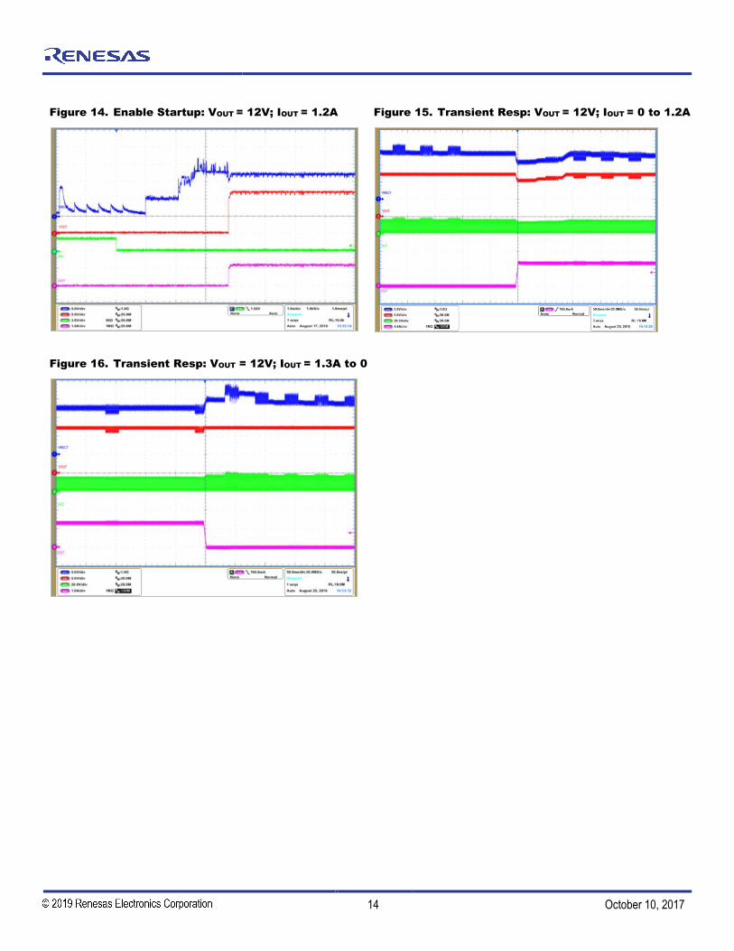
Figure 14. Enable Startup: VOUT = 12V; IOUT = 1.2A
Figure 15. Transient Resp: VOUT = 12V; IOUT = 0 to 1.2A
Figure 16. Transient Resp: VOUT = 12V; IOUT = 1.3A to 0

P9221-R Datasheet
© 2017 Integrated Device Technology, Inc. 15 October 10, 2017
7. Functional Block Diagram
Figure 17. Functional Block Diagram
EN
Syn
chro
nous
Rec
tifie
r C
ontr
ol
LDO
VRECT
SINK
OVP
32-bit ARM
Processor
AS
K M
odul
ator
BST1
AC1
AC2
OUT
VRECT
VOUT
ISNS
TS/EOC
ILIM
VOSET/Q-Fact
RPPO
RPPG
VTDIE
ADC MUX
I2C
Slave
SCL
SDA
Peak Detector
and LPF
VDD5VLDO
5V
LDO
1.8VVDD18
GND
ISN
S
UVLO
UV
LO
FS
K
Dem
odul
ator
Phase DetectorAC1
RSVx
EN
EN
EN
INT
BST2
COMM1
COMM2
ALIGNX
ALIGNY
DEN

P9221-R Datasheet
© 2017 Integrated Device Technology, Inc. 16 October 10, 2017
8. Theory of Operation
The P9221-R is a highly-integrated, wireless power receiver targeted for 15W applications. The device integrates a full-wave synchronous rectifier, low-dropout (LDO) linear regulator, and a 32-bit ARM®-based M0 microprocessor to manage all the digital control required to comply with the WPC-1.2.3 communication protocol.
Using the near-field inductive power transfer, the receiver converts the AC signal to a DC voltage using the integrated synchronous rectifier. The capacitor connected to the output of the rectifier smooths the full-wave rectified voltage into a DC voltage. After the internal biasing circuit is enabled, the “Synchronous Rectifier Control” block operates the switches of the rectifier in various modes to maintain reliable connections and optimal efficiency.
The rectifier voltage and the output current are sampled periodically and digitized by the analog-to-digital converter (ADC). The digital equivalents of the voltage and current are supplied to the internal control logic, which determines whether the loading conditions on the VRECT pin indicate that a change in the operating point is required. If the load is heavy enough and brings the voltage at VRECT below its target, the transmitter is set to a lower frequency that is closer to resonance and to a higher output power. If the voltage at VRECT is higher than its target, the transmitter is instructed to increase its frequency. To maximize efficiency, the voltage at VRECT is programmed to decrease as the LDO’s load current increases. The internal temperature is continuously monitored to ensure proper operation.
In the event that the VRECT voltage increases above 13.5V, the control loop disables the LDO and sends error packets to the transmitter in an attempt to bring the rectifier voltage back to a safe operating voltage level while simultaneously clamping the incoming energy using the open-drain SINK pin for VRECT linear clamping. The clamp is released when the VRECT voltage falls below the VOVP-DC minus VOVP-HYS. Refer to Figure 17. The receiver utilizes IDT’s proprietary voltage clamping scheme, which limits the maximum voltage at the rectifier pin to 13.5V, reducing the voltage rating on the output capacitors while eliminating the need for over-voltage protection (OVP) capacitors. As a result, it provides a small application area, making it an industry-leading wireless power receiver for high power density applications. Combined with the P9242-R transmitter, the P9221-R is a complete wireless power system solution.
8.1 LDO – Low Dropout Regulators
The P9221-R has three low-dropout linear regulators. The main regulator is used to provide the power required by the battery charger where the output voltage can be set to either 9V or 12V. For more information about setting the output voltage, see section 8.2. It is important to connect a minimum of 30µF ceramic capacitance to the OUT pin.
The other two regulators, VDD5V and VDD18, are to bias the internal circuitry of the receiver. The LDOs must have local 1µF ceramic capacitors placed as close as possible to the pins.
8.2 Setting the Output Voltage and Reference Q-factor Value – VOSET/Q-Fact Pin
The output voltage on the P9221-R is programmed by connecting the center tap of the external resistors R34 and R33 to the VOSET/Q-Fact pin as shown in the application schematic in Figure 24. The output voltage can be set to 9V or 12V. The recommended settings for R33 and R34 are summarized in Table 6.
The default output voltage is set to 12V in the P9221-R Evaluation Board (R34 = 10kΩ; R33 = open). . For applications where the transmitter is capable of delivering only 5W, the P9221-R will automatically switch to 5V output to ensure 5W power delivery. The 5W option can be disabled by changing the value of R33 as defined in Table 6. In this case, if the receiver is placed on a 5W transmitter, the receiver output pin will be high impedance.
This pin also allows for setting the Q-factor value by adjusting R34 and R33 as shown in Table 6. The default value is set to 103 on the P9221-R Evaluation Board. For development purposes, the Q-factor should be set to 20 to avoid prematurely triggering Q-factor.

P9221-R Datasheet
© 2017 Integrated Device Technology, Inc. 17 October 10, 2017
Table 6. Setting the Output Voltage and Reference Q-factor Value
Q Factor Value Setting
VOUT Setting(R34/R33 Values)
9V without 5V 9V with 5V 12V without 5V 12V with 5V
R34 R33 R34 R33 R34 R33 R34 R33
103 10kΩ 4.87kΩ Open 10kΩ 10kΩ 21kΩ 10kΩ Open
80 10kΩ 4.32kΩ 10kΩ 0.31kΩ 10kΩ 22.6kΩ 10kΩ 324kΩ
60 10kΩ 3.65kΩ 10kΩ 0.681kΩ 10kΩ 27.4kΩ 10kΩ 147kΩ
40 10kΩ 3.09kΩ 10kΩ 1.1kΩ 10kΩ 32.4kΩ 10kΩ 90.9kΩ
20 10kΩ 2.55kΩ 10kΩ 1.54kΩ 10kΩ 39.2kΩ 10kΩ 64.9kΩ
8.3 SINK Pin
The P9221-R has an internal automatic DC clamping to protect the device in the event of high voltage transients. The VRECT node must be connected to the SINK pin at all times using a 36Ω resistor with a greater than ¼ W rating.
8.4 Rectifier Voltage – VRECT
The P9221-R uses a high‐efficiency synchronous rectifier to convert the AC signal from the coil to a DC signal on the VRECT pin. During startup, the rectifier operates as a passive diode bridge. Once the voltage on VRECT exceeds the under-voltage lock-out level (UVLO; see Table 5), the rectifier will switch into full synchronous bridge rectifier mode. A total capacitance of 30μF is recommended to minimize the output voltage ripple. A 0.1uF capacitor is added for decoupling.
8.5 Over-Current Limit – ILIM
The P9221-R has a programmable current limit function for protecting the device in the event of an over-current or short-circuit fault condition. When the output current exceeds the programmed threshold (see Figure 11), the P9221-R will limit the load current by reducing the output voltage. The current limit should be set to 120% of the target maximum output current. See the ILIM pin description in Table 1 for further information. The ILIM pin allows changing the over-current limit value without modification of the firmware by selecting the values of R38 and R22 as shown in Table 7.
Table 7. Setting the Over Current Limit
Voltage on ILIM Pin [V] R38 [kΩ] R22 [kΩ] Output Current [A] Over-Current Limit [A]
Pull-up 10 Open 1.25 1.6
0.60 10 5.1 0.80 1
0.45 10 3.3 0.64 0.8
0.25 10 1.6 0.40 0.5

P9221-R Datasheet
© 2017 Integrated Device Technology, Inc. 18 October 10, 2017
8.6 Interrupt Function – INT
The P9221-R provides an open-drain, active-LOW interrupt output pin. It is asserted LOW when EN is HIGH or any of the following fault conditions have been triggered: the die temperature exceeds 140°C, the external thermistor measurement exceeds the threshold (see section 8.9), or an over-current (OC) or over-voltage (OV) condition is detected.
During normal operation, the INT pin is pulled HIGH. This pin can be connected to the interrupt pin of a microcontroller. The source of the trigger for the interrupt is available in the I2C Interrupt Status register (see Table 13).
8.7 Enable Pin – EN
The P9221-R can be disabled by applying a logic HIGH to the EN pin. When the EN pin is pulled HIGH, the device is in Shut-Down Mode.
Connecting the EN pin to logic LOW activates the device.
8.8 Thermal Protection
The P9221-R integrates thermal shutdown circuitry to prevent damage resulting from excessive thermal stress that may be encountered under fault conditions. This circuitry will shut down or reset the P9221-R if the die temperature exceeds 140°C.
8.9 External Temperature Sensing and End of Charge – TS/EOC
The P9221-R has a temperature sensor input which can be used to monitor an external temperature by using a thermistor. The built-in comparator’s reference voltage is 0.6V and 0.1V in the P9221-R, and it is used for monitoring the voltage level on the TS/EOC pin as described by Equation 1.
VTS=VVDD18×NTC
R+NTC Equation 1
Where NTC is the thermistor’s resistance and R is the pull-up resistor connected to VDD18 pin. The over–temperature shutdown is trigged when the TS pin voltage is between 0.6V and 0.1V; for more information, see Figure 24.
When the TS/EOC pin is less than 0.1V, the End of Charge (EOC) function is activated, and the P9221-R will send the End Power Transfer (EPT) packet to the transmitter terminating the power delivery.
8.10 Alignment Guide – ALIGNX and ALIGNY
This feature is used to provide directional information regarding the transmit coil and receive coil alignment while the wireless charger is in normal operation mode. Sensing coils (see the basic application circuit on the first page) are placed on the wireless power receiver side between the power Rx coil and power Tx coil. Special design enables the sensing coils to output zero voltage when the alignment is optimum while misalignment between the transmitter and receiver coils will result in a voltage on the sensing coils. These signals are internally rectified, filtered, and passed through the ADC providing quantitative information on the amount of misalignment. The higher the signal is, the more the coils are misaligned.
Furthermore, the signal magnitude on ALIGNX and ALIGNY provides directional information by measuring the phase between the input power AC signal and horizontal and vertical alignment signals. Once the signal passes through the ADC, the alignment information is represented by two 8-bit signed numbers, which can be read from the Alignment X Value and Alignment Y Value I2C registers defined in Table 22 and Table 23 respectively, which indicate the misalignment direction and magnitude.
The application processor can provide 2D visual graphics that suggest how much the power coils are misaligned in each direction and can suggest that the user move the device on the Tx pad for the best alignment to improve the power transferred and reduce the charging time.

P9221-R Datasheet
© 2017 Integrated Device Technology, Inc. 19 October 10, 2017
8.11 Advanced Foreign Object Detection (FOD)
When metallic objects are exposed to an alternating magnetic field, eddy currents cause such objects to heat up. Examples of such parasitic metal objects are coins, keys, paper clips, etc. The amount of heating depends on the strength of the coupled magnetic field, as well as on the characteristics of the object, such as its resistivity, size, and shape. In a wireless power transfer system, the heating manifests itself as a power loss, and therefore a reduction in power-transfer efficiency. Moreover, if no appropriate measures are taken, the heating could be sufficient that the foreign object could become heated to an unsafe temperature.
During the power transfer phase (see section 10.6), the receiver periodically communicates to the transmitter the amount of power received by means of a Received Power Packet (RPP). The transmitter will compare this power with the amount of power transmitted during the same time period. If there is a significant unexplained loss of power, then the transmitter will shut off power delivery because a possible foreign object might be absorbing too much energy.
For a WPC system to perform this function with sufficient accuracy, both the transmitter and receiver must account for and compensate for all of their known losses. Such losses could be due to resistive losses or nearby metals that are part of the transmitter or receiver, etc. Because the system accurately measures its power and accounts for all known losses, it can thereby detect foreign objects because they cause an unknown loss. The WPC specification requires that a power receiver must report to the power transmitter its received power (PPR) in an RPP. The maximum value of the received power accuracy 𝑃Δ depends on the maximum power of the power receiver as defined in Table 8.
The power receiver must determine its PPR with an accuracy of ±𝑃Δ, and report its received power as PRECEIVED = PPR + 𝑃Δ. This means that the reported received power is always greater than or equal to the transmitted power (PPT) if there is no foreign object (FO) present on the interface surface.
Table 8. Maximum Estimated Power Loss
Maximum Power [W] Maximum 𝑷𝚫 [mW]
15 750
The compensation algorithm includes values that are programmable via either the I2C interface or OTP (one-time programmable) bits. Programmability is necessary so that the calibration settings can be optimized to match the power transfer characteristics of each particular WPC system to include the power losses of the transmit and receive coils, battery, shielding, and case materials under no-load to full-load conditions. The values are based on the comparison of the received power against a reference power curve so that any foreign object can be sensed when the received power is different than the expected system power.

P9221-R Datasheet
© 2017 Integrated Device Technology, Inc. 20 October 10, 2017
8.12 Received Power Packet Offset and Gain Calibration – RPPO and RPPG
The received power packet offset (RPPO) and received power packet gain (RPPG) calibrations utilize dedicated pins for tuning foreign object detection (FOD). These calibrations tune the received power packet via the voltage levels on the RPPO and RPPG pins, which are determined by the external resistors in divider networks on the 1.8V bias voltage. The voltage level on the RPPO pin is used to add offset in order to shift the Received Power Packet (RPP) globally, and the voltage level on the RPPG pin adjusts the slope gain of the Received Power Packet (RPP).
The received power packet offset calibration can be tuned by varying the voltage on the RPPO pin from 0.1V to 2.1V corresponding to a power offset range from -1.56W to 2.34W.
The received power packet gain can be tuned by varying the voltage on the RPPG pin from 0.1V to 2.1V corresponding to a gain setting in the range from 0.111 to 2.33.
To disable the FOD, the RPP0 and RPPG must be connected to GND.
The RPP is adjusted according to Equation 2:
RPP [mW] = Pmeasured [mW] × RPPG [%]
1755 [%] + RPPO [mW] – 1755 [mW] Equation 2
Where
RPP = Received Power Packet
Pmeasured = measured power from output voltage and current
RPPO [mW] = VRPPO [V]
2.1 [V]× 4095 [mW] Equation 3
RPPG [%] = VRPPG [V]
2.1 [V]× 4095 [%] Equation 4
For example, if the voltage on the RPPO and RPPG pins is 0.9V then the RPP will have no offset or gain. The RPP will be exactly the same as the measured power in the receiver.

P9221-R Datasheet
© 2017 Integrated Device Technology, Inc. 21 October 10, 2017
9. Communication Interface
9.1 Modulation/Communication
The wireless medium power charging system uses two-way communication: receiver-to-transmitter and transmitter-to receiver.
Receiver-to-transmitter communication is accomplished by modulating the load seen by the receiver's inductor; the communication is purely digital and symbols 1’s and 0’s ride on top of the power signal that exists between the two coils. Modulation is done with amplitude-shift keying (ASK) modulation using internal switches to connect external capacitors from AC1 and AC2 to ground (see Figure 17) with a bit rate of 2Kbps. To the transmitter, this appears as an impedance change, which results in measurable variations of the transmitter’s output waveform. The power transmitter detects this as a modulation of coil current/voltage to receive the packets. See sections 9.2 and 9.3 for details for ASK modulation.
Transmitter-to-receiver communication is accomplished by frequency-shift keying (FSK) modulation over the power signal frequency. The power receiver P9221-R has the means to demodulate FSK data from the power signal frequency and use it in order to establish the handshaking protocol with the power transmitter.
The P9221-R implements FSK communication when used in conjunction with WPC-compliant transmitters, such as the P9242-R. The FSK communication protocol allows the transmitter to send data to the receiver using the power transfer link in the form of modulating the power transfer signal. This modulation appears in the form of a change in the base operating frequency (fOP) to the modulated operating frequency (fMOD) in periods of 256 consecutive cycles. Equation 5 should be used to compute the modulated frequency based on any given operating frequency. The P9221-R will only implement positive FSK polarity adjustments; in other words, the modulated frequency will always be higher than the operating frequency during FSK communication.
Communication packets are transmitted from transmitter to receiver with less than 1% positive frequency deviation following any receiver-to-transmitter communication packet. The frequency deviation is calculated using Equation 5.
fMOD=60000
60000fOP
− 3
[KHz] Equation 5
Where fMOD is the changed frequency in the power signal frequency; fOP is the base operating frequency of the power transfer; and 60000kHz is the internal oscillator responsible for counting the period of the power transfer signal.
The FSK byte-encoding scheme and packet structure comply with the WPC specification revision 1.2.3. The FSK communication uses a bi-phase encoding scheme to modulate data bits into the power transfer signal. The start bit will consist of 512 consecutive fMOD cycles (or logic ‘0’). A logic ‘1’ value will be sent by sending 256 consecutive fOP cycles followed by 256 fMOD cycles or vice versa, and a logic ‘0’ is sent by sending 512 consecutive fMOD or fOP cycles.
Figure 18. Example of Differential Bi-phase Decoding for FSK
tCLK = 256/fOP
ONE ZERO ONE ZERO ONE ONE ZERO ZERO
512 cycles 256 cycles
Each byte will comply with the start, data, parity, and stop asynchronous serial format structure shown in Figure 19:
Figure 19. Example of Asynchronous Serial Byte Format for FSK
Start StopParityb0 1 2 3 4 5 6 7b b b b b b b

P9221-R Datasheet
© 2017 Integrated Device Technology, Inc. 22 October 10, 2017
9.2 Bit Encoding Scheme for ASK
As required by the WPC, the P9221-R uses a differential bi-phase encoding scheme to modulate data bits onto the power signal. A clock frequency of 2kHz is used for this purpose. A logic ONE bit is encoded using two narrow transitions, whereas a logic ZERO bit is encoded using one wider transition as shown below:
Figure 20. Bit Encoding Scheme
tCLK
ONE ZERO ONE ZERO ONE ONE ZERO ZERO
9.3 Byte Encoding for ASK
Each byte in the communication packet comprises 11 bits in an asynchronous serial format, as shown in Figure 21.
Figure 21. Byte Encoding Scheme
Start StopParityb0 1 2 3 4 5 6 7b b b b b b b
Each byte has a start bit, 8 data bits, a parity bit, and a single stop bit.
9.4 Packet Structure
The P9221-R communicates with the base station via communication packets. Each communication packet has the following structure:
Figure 22. Communication Packet Structure
Preamble Header Message Checksum
P9221-R Datasheet
© 2017 Integrated Device Technology, Inc. 23 October 10, 2017
10. WPC Mode Characteristics
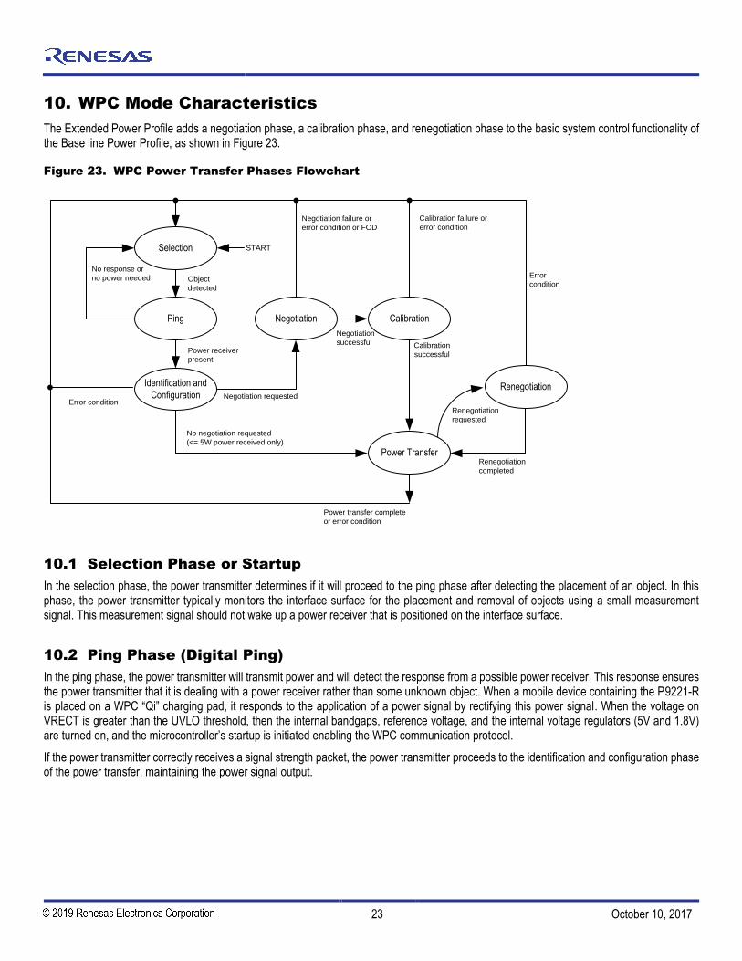
The Extended Power Profile adds a negotiation phase, a calibration phase, and renegotiation phase to the basic system control functionality of the Base line Power Profile, as shown in Figure 23.
Figure 23. WPC Power Transfer Phases Flowchart
START
Object
detected
Error condition
Negotiation failure or
error condition or FOD
Calibration
successful
Negotiation
successful
Negotiation requested
No negotiation requested
(<= 5W power received only)
Renegotiation
completed
Calibration failure or
error condition
No response or
no power needed
Selection
Ping
Identification and
Configuration
Negotiation
Renegotiation
Calibration
Power Transfer
Power receiver
present
Power transfer complete
or error condition
Renegotiation
requested
Error
condition
10.1 Selection Phase or Startup
In the selection phase, the power transmitter determines if it will proceed to the ping phase after detecting the placement of an object. In this phase, the power transmitter typically monitors the interface surface for the placement and removal of objects using a small measurement signal. This measurement signal should not wake up a power receiver that is positioned on the interface surface.
10.2 Ping Phase (Digital Ping)
In the ping phase, the power transmitter will transmit power and will detect the response from a possible power receiver. This response ensures the power transmitter that it is dealing with a power receiver rather than some unknown object. When a mobile device containing the P9221-R is placed on a WPC “Qi” charging pad, it responds to the application of a power signal by rectifying this power signal. When the voltage on VRECT is greater than the UVLO threshold, then the internal bandgaps, reference voltage, and the internal voltage regulators (5V and 1.8V) are turned on, and the microcontroller’s startup is initiated enabling the WPC communication protocol.
If the power transmitter correctly receives a signal strength packet, the power transmitter proceeds to the identification and configuration phase of the power transfer, maintaining the power signal output.
P9221-R Datasheet
© 2017 Integrated Device Technology, Inc. 24 October 10, 2017
10.3 Identification and Configuration Phase
The identification and configuration phase is the part of the protocol that the power transmitter executes in order to identify the power receiver and establish a default power transfer contract. This protocol extends the digital ping in order to enable the power receiver to communicate the relevant information.
In this phase, the power receiver identifies itself and provides information for a default power transfer contract:
It sends the configuration packet.
If the power transmitter does not acknowledge the request (does not transmit FSK modulation), the power receiver will assume 5W output power.
10.4 Negotiation Phase
In the negotiation phase, the power receiver negotiates changes to the default power transfer contract. In addition, the power receiver verifies that the power transmitter has not detected a foreign object.
10.5 Calibration Phase
In the calibration phase, the power receiver provides information that the power transmitter can use to improve its ability to detect foreign objects during power transfer.
10.6 Power Transfer Phase
In this phase, the P9221-R controls the power transfer by means of the following control data packets:
Control Error Packets
Received Power Packet (RPP, FOD-related)
End Power Transfer (EPT) Packet
Once the “identification and configuration” phase is completed, the transmitter initiates the power transfer mode. The P9221-R control circuit measures the rectifier voltage and sends error packets to the transmitter to adjust the rectifier voltage to the level required to maximize the efficiency of the linear regulator and to send to the transmitter the actual received power packet for foreign object detection (FOD) to guarantee safe, efficient power transfer.
In the event of an EPT issued by the application, the P9221-R turns off the LDO and continuously sends EPT packets until the transmitter removes the power and the rectified voltage on the receiver side drops below the UVLO threshold.
P9221-R Datasheet
© 2017 Integrated Device Technology, Inc. 25 October 10, 2017
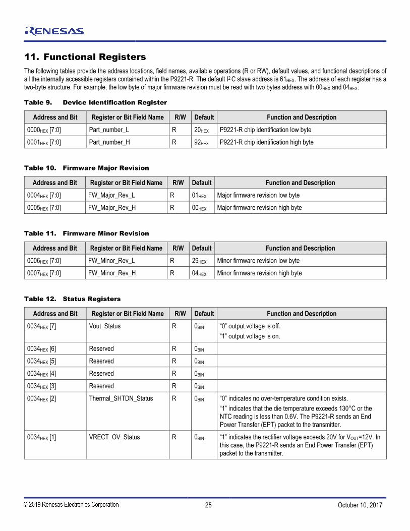
11. Functional Registers
The following tables provide the address locations, field names, available operations (R or RW), default values, and functional descriptions of all the internally accessible registers contained within the P9221-R. The default I2 C slave address is 61HEX. The address of each register has a two-byte structure. For example, the low byte of major firmware revision must be read with two bytes address with 00HEX and 04HEX.
Table 9. Device Identification Register
Address and Bit Register or Bit Field Name R/W Default Function and Description
0000HEX [7:0] Part_number_L R 20HEX P9221-R chip identification low byte
0001HEX [7:0] Part_number_H R 92HEX P9221-R chip identification high byte
Table 10. Firmware Major Revision
Address and Bit Register or Bit Field Name R/W Default Function and Description
0004HEX [7:0] FW_Major_Rev_L R 01HEX Major firmware revision low byte
0005HEX [7:0] FW_Major_Rev_H R 00HEX Major firmware revision high byte
Table 11. Firmware Minor Revision
Address and Bit Register or Bit Field Name R/W Default Function and Description
0006HEX [7:0] FW_Minor_Rev_L R 29HEX Minor firmware revision low byte
0007HEX [7:0] FW_Minor_Rev_H R 04HEX Minor firmware revision high byte
Table 12. Status Registers
Address and Bit Register or Bit Field Name R/W Default Function and Description
0034HEX [7] Vout_Status R 0BIN “0” output voltage is off.
“1” output voltage is on.
0034HEX [6] Reserved R 0BIN
0034HEX [5] Reserved R 0BIN
0034HEX [4] Reserved R 0BIN
0034HEX [3] Reserved R 0BIN
0034HEX [2] Thermal_SHTDN_Status R 0BIN “0” indicates no over-temperature condition exists.
“1” indicates that the die temperature exceeds 130°C or the NTC reading is less than 0.6V. The P9221-R sends an End Power Transfer (EPT) packet to the transmitter.
0034HEX [1] VRECT_OV_Status R 0BIN “1” indicates the rectifier voltage exceeds 20V for VOUT=12V. In this case, the P9221-R sends an End Power Transfer (EPT) packet to the transmitter.

P9221-R Datasheet
© 2017 Integrated Device Technology, Inc. 26 October 10, 2017
Address and Bit Register or Bit Field Name R/W Default Function and Description
0034HEX [0] Current_Limit_Status R 0BIN “1” indicates the current limit has been exceeded. In this case, the P9221-R sends an End Power Transfer (EPT) packet to the transmitter.
0035HEX [7:0] Reserved R 00HEX
Table 13. Interrupt Status Registers
Address and Bit Register or Bit Field Name R/W Default Function and Description
0036HEX [7] INT_Vout_Status R 0BIN “0” indicates the output voltage has not changed.
“1” indicates the output voltage changed.
0036HEX [6] Reserved R 0BIN
0036HEX [5] Reserved R 0BIN
0036HEX [4] Reserved R 0BIN
0036HEX [3] Reserved R 0BIN
0036HEX [2] INT_OVER_TEMP_Status R 0BIN “1” indicates an over-temperature condition exists.
0036HEX [1] INT_VRECT_OV_Status R 0BIN “1” indicates a rectifier over-voltage condition exists.
0036HEX [0] INT_OC_Limit_Status R 0 “1” indicates the current limit has been exceeded.
0037HEX [7:0] Reserved R 00HEX
Note: If any bit in the Interrupt Status register 36HEX is “1” and the corresponding bit in the Interrupt Enable register 38HEX is set to “1,” the
INT pin will be pulled down indicating an interrupt event has occurred.
Table 14. Interrupt Enable Registers
Address and Bit Register or Bit Field Name R/W Default Function and Description
0038HEX [7] Vout_Status_INT_EN RW 0BIN “0” disables the INT_Vout_Status interrupt.
"1" enables the interrupt.
0038HEX [6] Reserved R 0BIN
0038HEX [5] Reserved R 0BIN
0038HEX [4] Reserved R 1BIN
0038HEX [3] Reserved R 1BIN
0038HEX [2] OVER_TEMP_INT_EN R 1BIN “0” disables the INT_OVER_TEMP interrupt.
"1" enables the interrupt.
0038HEX [1] VRECT_OV_INT_EN RW 1BIN “0” disables the INT_VRECT_OV interrupt.
"1" enables the interrupt.
0038HEX [0] OC_Limit_Status_INT_EN RW 1BIN “0” disables the INT_OC_Limit_Status interrupt.
"1" enables the interrupt.
0039HEX [7:0] Reserved RW 00HEX
P9221-R Datasheet
© 2017 Integrated Device Technology, Inc. 27 October 10, 2017
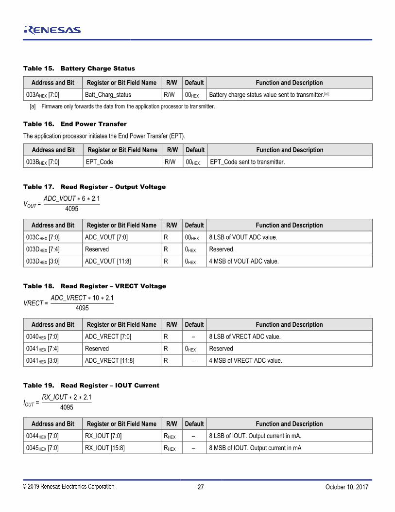
Table 15. Battery Charge Status
Address and Bit Register or Bit Field Name R/W Default Function and Description
003AHEX [7:0] Batt_Charg_status R/W 00HEX Battery charge status value sent to transmitter.[a]
[a] Firmware only forwards the data from the application processor to transmitter.
Table 16. End Power Transfer
The application processor initiates the End Power Transfer (EPT).
Address and Bit Register or Bit Field Name R/W Default Function and Description
003BHEX [7:0] EPT_Code R/W 00HEX EPT_Code sent to transmitter.
Table 17. Read Register – Output Voltage
VOUT = ADC_VOUT ∗ 6 ∗ 2.1
4095
Address and Bit Register or Bit Field Name R/W Default Function and Description
003CHEX [7:0] ADC_VOUT [7:0] R 00HEX 8 LSB of VOUT ADC value.
003DHEX [7:4] Reserved R 0HEX Reserved.
003DHEX [3:0] ADC_VOUT [11:8] R 0HEX 4 MSB of VOUT ADC value.
Table 18. Read Register – VRECT Voltage
VRECT = ADC_VRECT ∗ 10 ∗ 2.1
4095
Address and Bit Register or Bit Field Name R/W Default Function and Description
0040HEX [7:0] ADC_VRECT [7:0] R – 8 LSB of VRECT ADC value.
0041HEX [7:4] Reserved R 0HEX Reserved
0041HEX [3:0] ADC_VRECT [11:8] R – 4 MSB of VRECT ADC value.
Table 19. Read Register – IOUT Current
IOUT = RX_IOUT ∗ 2 ∗ 2.1
4095
Address and Bit Register or Bit Field Name R/W Default Function and Description
0044HEX [7:0] RX_IOUT [7:0] RHEX – 8 LSB of IOUT. Output current in mA.
0045HEX [7:0] RX_IOUT [15:8] RHEX – 8 MSB of IOUT. Output current in mA
P9221-R Datasheet
© 2017 Integrated Device Technology, Inc. 28 October 10, 2017
Table 20. Read Register – Die Temperature
TDIE=(ADC_Die_Temp − 1350)83
444 – 273 where ADC_Die_Temp = 12 bits from ADC_Die_Temp_H and ADC_Die_Temp_L
Address and Bit Register or Bit Field Name R/W Default Function and Description
0046HEX [7:0] ADC_Die_Temp_L R - 8 LSB of current die temperature in °C.
0047HEX [7:4] Reserved R 0HEX Reserved
0047HEX [3:0] ADC_Die_Temp_H R - 4 MSB of current die temperature in °C.
Table 21. Read Register – Operating Frequency
fOP=64 ∗ 6000
OP_FREQ [15:0]
Address and Bit Register or Bit Field Name R/W Default Function and Description
0048HEX [7:0] OP_FREQ[15:8] R - 8 MSB of the AC signal frequency [kHz].
0049HEX [7:0] OP_FREQ[7:0] R - 8 LSB of the AC signal frequency [kHz].
Table 22. Alignment X Value Register
Note: Valid only in presence of the alignment PCB coil. (See section 8.10 or the P9221-R Evaluation Kit User Manual for more information.)
Address and Bit Register or Bit Field Name R/W Default Function and Description
004BHEX [7:0] Align_X R - 8-bit signed integer representing alignment between Tx and Rx coil in the X-direction. The value is application-specific.
Table 23. Alignment Y Value Register
Note: Valid only in the presence of the alignment PCB coil. (See section 8.10 or the P9221-R Evaluation Kit User Manual for more information.)
Address and Bit Register or Bit Field Name R/W Default Function and Description
004CHEX [7:0] Align_Y R - 8-bit signed integer representing alignment between Tx and Rx coil in the Y-direction. The value is application-specific.

P9221-R Datasheet
© 2017 Integrated Device Technology, Inc. 29 October 10, 2017
Table 24. Command Register
Address and Bit Register Field Name R/W Default Function and Description
004EHEX [7:6] Reserved R 0HEX Reserved.
004EHEX [5] Clear_Interrupt RW 0HEX If application processor sets this bit to "1," the P9221-R clears the interrupt pin.
004EHEX [4] Send_Battery_Charge_Status packet
R 0HEX If the application processor sets this bit to "1,” the P9221-R sends the charge status packet once (from the Batt_Charge_status register; see Table 15) and then sets this bit to “0.”
004EHEX [3] Send_End_Power_Transfer RW 0HEX If application processor sets this bit to "1," the P9221-R sends the end power transfer packet (defined in the EPT_Code register in Table 16) to the transmitter and then sets this bit to "0."
004EHEX [2] Reserved R 0HEX Reserved
004EHEX [1] Toggle_LDO_On-OFF RW 0HEX If application processor sets this bit to "1,” the P9221-R toggles the LDO output once (from on to off or from off to on), and then sets this bit to “0.”
004EHEX [0] Reserved R 0HEX Reserved
12. Application Information
12.1 Power Dissipation and Thermal Requirements
The use of integrated circuits in low-profile and fine-pitch surface-mount packages requires special attention to power dissipation. Many system-dependent issues such as thermal coupling, airflow, added heat sinks, convection surfaces, and the presence of other heat-generating components must be taken into consideration.
The P9221-R package has a maximum power dissipation of approximately 1.72W, which is governed by the number of thermal vias between the package and the printed circuit board. The die’s maximum power dissipation is specified by the junction temperature and the package thermal resistance. The WLCSP package has a typical θJA of 47ºC/W with 8 thermal vias and 77ºC/W with no thermal vias. Maximizing the thermal vias is highly recommended.
The ambient temperature surrounding the P9221-R will also have an effect on the thermal limits of the printed circuit board (PCB). The main factors influencing thermal resistance (θJA) are the PCB characteristics and thermal vias. For example, in a typical still-air environment, a significant amount of the heat generated is absorbed by the PCB. Changing the design or configuration of the PCB changes the overall thermal resistivity and therefore the board’s heat-sinking efficiency.
Three basic approaches for enhancing thermal performance are listed below:
Improving the power dissipation capability of the PCB design
Improving the thermal coupling of the component to the PCB.
Introducing airflow into the system.
P9221-R Datasheet
© 2017 Integrated Device Technology, Inc. 30 October 10, 2017
First, the maximum power dissipation for a given situation should be calculated using Equation 6:
PD(MAX) =(TJ(MAX) − TAMB)
θJA
Equation 6
Where PD(MAX) = Maximum power dissipation
θJA = Package thermal resistance (°C/W)
TJ(MAX) = Maximum device junction temperature (°C)
TAMB = Ambient temperature (°C)
The maximum recommended junction temperature (TJ(MAX)) for the P9221-R device is 125°C. The thermal resistance of the 52-WLCSP package (AHG52) is nominally θJA=47°C/W with 8 thermal vias. Operation is specified to a maximum steady-state ambient temperature (TAMB) of 85°C. Therefore, the maximum recommended power dissipation is given by Equation 7.
PD(MAX) = (124°C − 85°C)
47°C/W≅ 0.85 Watt Equation 7
All the above-mentioned thermal resistances were determined with the P9221-R mounted on a standard board of the dimensions and characteristics specified by the JEDEC 51 standard.
12.2 Recommended Coils
The following coils are recommended with the P9221-R receiver for 15W applications for optimum performance. The recommended vendor coils have been tested and verified as shown in Table 25.
Table 25. Recommended Coil Manufacturers
Output Power Vendor Part number Inductance at 100kHz ACR at 20°C Series Resonant Capacitance
15W AMOTECH ASC-504060E00-S00 8.2µH 220mΩ 400nF
15W TDK WR424245-13K2-G 11.2µH 170mΩ 300nF
15W SUNLORD SWA50R40H06C02B 8.4µH 150mΩ 400nF
15W WURTH 760308102207 8.0µH 80mΩ 400nF
P9221-R Datasheet
© 2017 Integrated Device Technology, Inc. 31 October 10, 2017
D1
LE
D
C1
2
NP
C1
0
10uF
INT
INT
SD
A
C9
3.3
nF
R1
8
NP
VD
D5
V
D6
5.1
VR
80
RS
V1
C2
5N
P
ALG
X
R3
3
NP
R3
9
10k
C1
90
.1u
F
C2
1
10uF
C1
615nF
U1
P9221-R
CO
MM
1A
1
CO
MM
2A
6
RS
V4
B1
RS
V5
B6
EN
B5
ALIGNXA2
SCLA3
VO
SE
T/Q
-Fa
ct
A4
RP
PG
A5
SDAB3
ALIGNYB2
ILIM
B4
RP
PO
C4
RS
V6
C5
OU
TD
1
INTC3
SINKC2
OU
T1
D2
OU
T2
D3
OU
T3
D4
OU
T4
D5
OU
T5
D6
VR
EC
TE
1
VR
EC
T1
E2
VR
EC
T2
E5
VR
EC
T3
E6
VR
EC
T4
F2
VR
EC
T5
F3
VR
EC
T6
F4
VR
EC
T7
F5
AC
1G
2
AC
1_
1H
1
AC
1_
2H
2
AC
2G
5
AC
2_
1H
5
AC
2_
2H
6
BS
T1
G1
BS
T2
G6
PGNDC1
PGND1C6
PGND2J1
PGND3J2
PGND4J3
PGND5J4
PGND6J5
PGND7J6
VD
D5
VF
1
VD
D1
8F
6
RSV3G3
RSV2H3
RSV1G4
TS/EOCH4
C2
01uF
/EN
R1
910K
I2C
RA
IL
VO
UT
VO
SE
T
P9221-R MM EV Board V2.2
C3
1
0.1
uF
C8
15nF
VR
EC
T
R3
50
J1
I2C
1 2 3 4 5
L1
SC
L
R2
8N
P
R1
710k
VP
P18
R4
2
NP
VD
D5
V
R2
2
NP
R2
36
R1
45
.1k
C3
10
0n
F/5
0V
RP
O
C1
1
10uF
RSV1
R1
35
.1k
TS
VO
UT
C2
3
0.1
uF
GN
D1
R1
610K
VR
EC
T
R2
9
10K
C7
NP
VO
SN
S
ILIM
R3
410k
R2
3
10k
C2
2
10uF
VD
D5
V
R3
810K
RX Power Coil
AlignX coil
C1
8 1uF
C6
47nF
VP
P18
Vre
ct
R1
5.1
k
ALG
Y
TS
C2
10
0n
F/5
0V
D7
5.1
V
U2
NP
A0
1
A1
2
A2
3
VS
S4
SD
A5
SC
L6
WP
7
VC
C8
E_PAD9
VP
P18
RT
S
NP
VP
P18
C1
10
0n
F/5
0V
AlignY coil
WP
C5
10
0n
F/5
0V
R4
1
NP
LC
SD
A
INT
R2
7
10K
VO
UT
C3
3
10uF
DE
N
R3
0N
P
AC
2T
TS
C1
5N
PG
ND
SC
L
R6
NP
R1
510K
GC
OM
AC
2
RP
G
C1
447nF
12.3 Typical Application Schematic
Figure 24. Typical Application Schematic – P9221-R Evaluation Board Revision 2.2
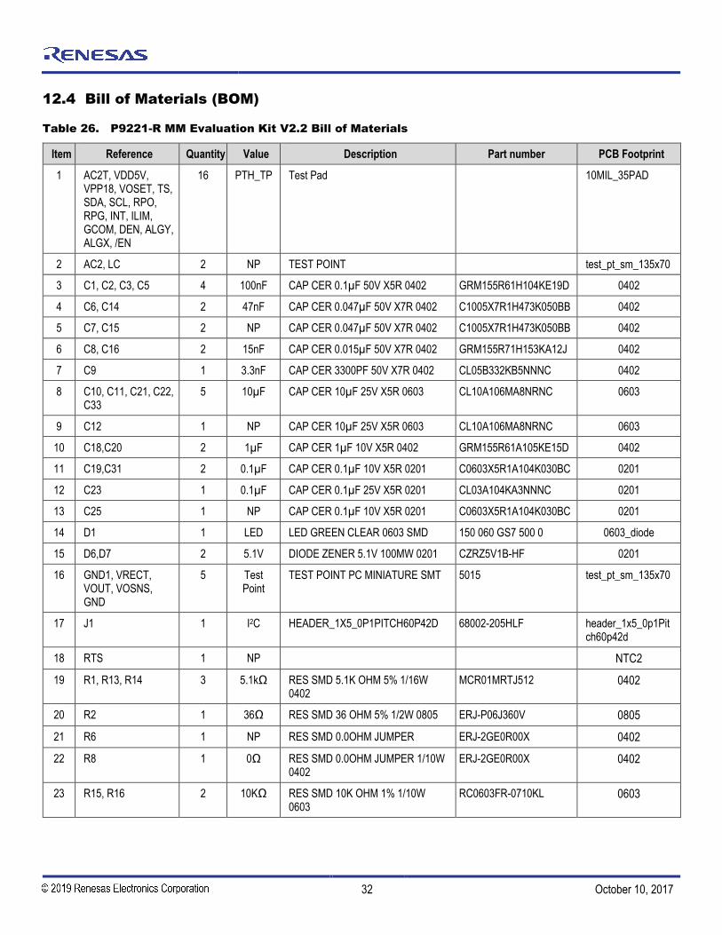
P9221-R Datasheet
© 2017 Integrated Device Technology, Inc. 32 October 10, 2017
12.4 Bill of Materials (BOM)
Table 26. P9221-R MM Evaluation Kit V2.2 Bill of Materials
Item Reference Quantity Value Description Part number PCB Footprint
1 AC2T, VDD5V, VPP18, VOSET, TS, SDA, SCL, RPO, RPG, INT, ILIM, GCOM, DEN, ALGY, ALGX, /EN
16 PTH_TP Test Pad
10MIL_35PAD
2 AC2, LC 2 NP TEST POINT
test_pt_sm_135x70
3 C1, C2, C3, C5 4 100nF CAP CER 0.1µF 50V X5R 0402 GRM155R61H104KE19D 0402
4 C6, C14 2 47nF CAP CER 0.047µF 50V X7R 0402 C1005X7R1H473K050BB 0402
5 C7, C15 2 NP CAP CER 0.047µF 50V X7R 0402 C1005X7R1H473K050BB 0402
6 C8, C16 2 15nF CAP CER 0.015µF 50V X7R 0402 GRM155R71H153KA12J 0402
7 C9 1 3.3nF CAP CER 3300PF 50V X7R 0402 CL05B332KB5NNNC 0402
8 C10, C11, C21, C22, C33
5 10µF CAP CER 10µF 25V X5R 0603 CL10A106MA8NRNC 0603
9 C12 1 NP CAP CER 10µF 25V X5R 0603 CL10A106MA8NRNC 0603
10 C18,C20 2 1µF CAP CER 1µF 10V X5R 0402 GRM155R61A105KE15D 0402
11 C19,C31 2 0.1µF CAP CER 0.1µF 10V X5R 0201 C0603X5R1A104K030BC 0201
12 C23 1 0.1µF CAP CER 0.1µF 25V X5R 0201 CL03A104KA3NNNC 0201
13 C25 1 NP CAP CER 0.1µF 10V X5R 0201 C0603X5R1A104K030BC 0201
14 D1 1 LED LED GREEN CLEAR 0603 SMD 150 060 GS7 500 0 0603_diode
15 D6,D7 2 5.1V DIODE ZENER 5.1V 100MW 0201 CZRZ5V1B-HF 0201
16 GND1, VRECT, VOUT, VOSNS, GND
5 Test Point
TEST POINT PC MINIATURE SMT 5015 test_pt_sm_135x70
17 J1 1 I2C HEADER_1X5_0P1PITCH60P42D 68002-205HLF header_1x5_0p1Pitch60p42d
18 RTS 1 NP
NTC2
19 R1, R13, R14 3 5.1kΩ RES SMD 5.1K OHM 5% 1/16W 0402
MCR01MRTJ512 0402
20 R2 1 36Ω RES SMD 36 OHM 5% 1/2W 0805 ERJ-P06J360V 0805
21 R6 1 NP RES SMD 0.0OHM JUMPER ERJ-2GE0R00X 0402
22 R8 1 0Ω RES SMD 0.0OHM JUMPER 1/10W 0402
ERJ-2GE0R00X 0402
23 R15, R16 2 10KΩ RES SMD 10K OHM 1% 1/10W 0603
RC0603FR-0710KL 0603
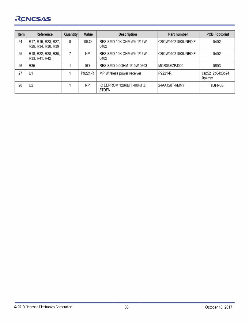
P9221-R Datasheet
© 2017 Integrated Device Technology, Inc. 33 October 10, 2017
Item Reference Quantity Value Description Part number PCB Footprint
24 R17, R19, R23, R27, R29, R34, R38, R39
8 10kΩ RES SMD 10K OHM 5% 1/16W 0402
CRCW040210K0JNEDIF 0402
25 R18, R22, R28, R30, R33, R41, R42
7 NP RES SMD 10K OHM 5% 1/16W 0402
CRCW040210K0JNEDIF 0402
26 R35 1 0Ω RES SMD 0.0OHM 1/10W 0603 MCR03EZPJ000 0603
27 U1 1 P9221-R MP Wireless power receiver P9221-R csp52_2p64x3p94_0p4mm
28 U2 1 NP IC EEPROM 128KBIT 400KHZ 8TDFN
24AA128T-I/MNY TDFN08

P9221-R Datasheet
© 2017 Integrated Device Technology, Inc. 34 October 10, 2017
13. Package Drawings
Figure 25. Package Outline Drawing (AHG52)
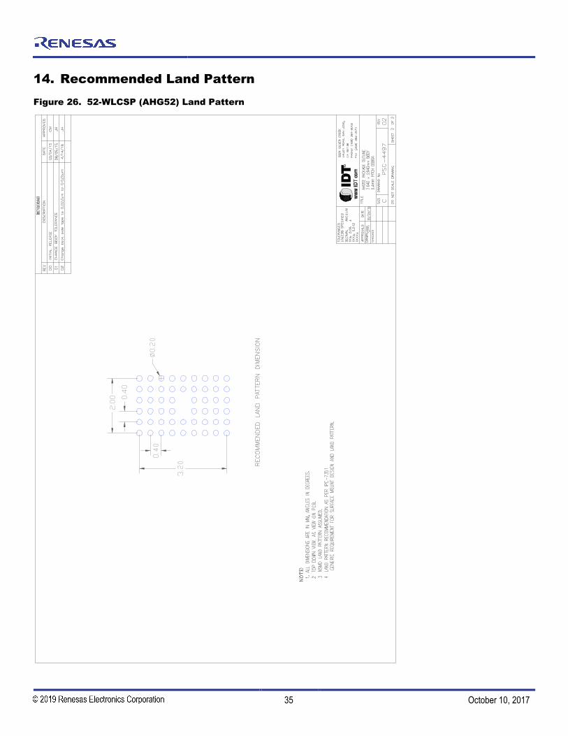
P9221-R Datasheet
© 2017 Integrated Device Technology, Inc. 35 October 10, 2017
14. Recommended Land Pattern
Figure 26. 52-WLCSP (AHG52) Land Pattern

P9221-R Datasheet
© 2017 Integrated Device Technology, Inc. 36 October 10, 2017
15. Special Notes: WLCSP-52 (AHG52) Package Assembly
Unopened dry packaged parts have a one-year shelf life.
The HIC indicator card for newly-opened dry packaged parts should be checked. If there is any moisture content, the parts must be baked for a minimum of 8 hours at 125˚C within 24 hours of the assembly reflow process.
16. Marking Diagram
IDTP9221YYWW**$-R
1. Line 1 company name.
2. Truncated part number.
3. “YYWW” is the last digit of the year and week that the part was assembled.
** is the lot sequential code.
4. “$” denotes mark code, -R is part of the device part number
17. Ordering Information
Orderable Part Number Description and Package MSL Rating Shipping Packaging Ambient
Temperature
P9221-RAHGI8 P9221-R Wireless Power Receiver for 15W
Applications, 2.64 3.94 mm 52-WLCSP (AHG52)
MSL1 Tape and reel 0°C to +85°C
P9221-R-EVK P9221-R-EVK Evaluation Board

P9221-R Datasheet
© 2017 Integrated Device Technology, Inc. 37 October 10, 2017
18. Revision History
Revision Date Description of Change
October 10, 2017 Initial release
Corporate Headquarters
6024 Silver Creek Valley Road San Jose, CA 95138 www.IDT.com
Sales
1-800-345-7015 or 408-284-8200 Fax: 408-284-2775 www.IDT.com/go/sales
Tech Support
www.IDT.com/go/support
DISCLAIMER Integrated Device Technology, Inc. (IDT) and its affiliated companies (herein referred to as “IDT”) reserve the right to modify the products and/or specifications described herein at any time, without notice, at IDT's sole discretion. Performance specifications and operating parameters of the described products are determined in an independent state and are not guaranteed to perform the same way when installed in customer products. The information contained herein is provided without representation or warranty of any kind, whether express or implied, including, but not limited to, the suitability of IDT's products for any particular purpose, an implied warranty of merchantability, or non -infringement of the intellectual property rights of others. This document is presented only as a guide and does not convey any license under intellectual property rights of IDT or any third parties. IDT's products are not intended for use in applications involving extreme environmental conditions or in life support systems or similar devices where the failure or malfunction of an IDT product can be reasonably expected to significantly affect the health or safety of users. Anyone using an IDT product in such a manner does so at their own risk, absent an express, written agreement by IDT. Integrated Device Technology, IDT and the IDT logo are trademarks or registered trademarks of IDT and its subsidiaries in the Uni ted States and other countries. Other trademarks used herein are the property of IDT or their respective third party owners. For datasheet type definitions and a glossary of common terms, visit www.idt.com/go/glossary. All contents of this document are copyright of Integrated Device Technology, Inc. All rights reserved.

Corporate HeadquartersTOYOSU FORESIA, 3-2-24 Toyosu,Koto-ku, Tokyo 135-0061, Japanwww.renesas.com
Contact InformationFor further information on a product, technology, the most up-to-date version of a document, or your nearest sales office, please visit:www.renesas.com/contact/
TrademarksRenesas and the Renesas logo are trademarks of Renesas Electronics Corporation. All trademarks and registered trademarks are the property of their respective owners.
IMPORTANT NOTICE AND DISCLAIMER
RENESAS ELECTRONICS CORPORATION AND ITS SUBSIDIARIES (“RENESAS”) PROVIDES TECHNICAL SPECIFICATIONS AND RELIABILITY DATA (INCLUDING DATASHEETS), DESIGN RESOURCES (INCLUDING REFERENCE DESIGNS), APPLICATION OR OTHER DESIGN ADVICE, WEB TOOLS, SAFETY INFORMATION, AND OTHER RESOURCES “AS IS” AND WITH ALL FAULTS, AND DISCLAIMS ALL WARRANTIES, EXPRESS OR IMPLIED, INCLUDING, WITHOUT LIMITATION, ANY IMPLIED WARRANTIES OF MERCHANTABILITY, FITNESS FOR A PARTICULAR PURPOSE, OR NON-INFRINGEMENT OF THIRD PARTY INTELLECTUAL PROPERTY RIGHTS.
These resources are intended for developers skilled in the art designing with Renesas products. You are solely responsible for (1) selecting the appropriate products for your application, (2) designing, validating, and testing your application, and (3) ensuring your application meets applicable standards, and any other safety, security, or other requirements. These resources are subject to change without notice. Renesas grants you permission to use these resources only for development of an application that uses Renesas products. Other reproduction or use of these resources is strictly prohibited. No license is granted to any other Renesas intellectual property or to any third party intellectual property. Renesas disclaims responsibility for, and you will fully indemnify Renesas and its representatives against, any claims, damages, costs, losses, or liabilities arising out of your use of these resources. Renesas' products are provided only subject to Renesas' Terms and Conditions of Sale or other applicable terms agreed to in writing. No use of any Renesas resources expands or otherwise alters any applicable warranties or warranty disclaimers for these products.
(Rev.1.0 Mar 2020)
© 2020 Renesas Electronics Corporation. All rights reserved.