Embed Size (px)
Citation preview

AN32258A
Page 1 of 30
Product Standards
Ver.2.00
INTEGRATED WIRELESS POWER SUPPLY RECEIVER,
Qi (WIRELESS POWER CONSORTIUM) COMPLIANT
― AN32258A ―
Wireless Power System
http://www.semicon.panasonic.co.jp/en/
Cd
Control
Cs
RXCoil
Cp
Rec
tifie
r
TXCoil
Wireless Power
Communication
VRECT
Tx
Inve
rter
VIN
+
OUT
Transmitter (Tx) Receiver (Rx)
AN32258
Charger
NN32251
Co
IOUT
Integrated Wireless Power Receiver Solution
WPC Ver. 1.1 Compliant
Synchronous Full Bridge Rectifier Control
Input Voltage Range : VRECT = 4.4 V to 19 V
Output Voltage: 5 V
Temperature Detecting Circuit
Full Charge Detection with Adjustable Current Level
Switching Control of External Power Supply
Supports Under Voltage Lockout , Thermal Shutdown,
Over Voltage Detection, and Over Current Detection.
LED Indicator
3.16 mm X 3.16 mm WLCSP
48 Pins with 0.4mm pitch
・WPC Compliant Receivers
・Cell Phones, Smartphones
・Headsets
・Digital Cameras
・Tablet Devices
・Portable Media Players etc.
APPLICATIONS
FEATURES DESCRIPTION
AN32258A is a wireless power system controller IC which is compliant with Qi version 1.1 of the System Description Wireless Power Transfer, Volume 1 for Low Power defined by Wireless Power Consortium. AN32258A is a controller IC of a power receiver (Rx) which can be used with any Qi-compliant wireless chargers.
AN32258A is designed to be used based on
the circuits and external components described in this
document and Application Note. Therefore, Panasonic
cannot support any inquiries of modified solution.
IMPORTANT
Doc No. TA4-EA-06273Revision. 1
Established : 2014-10-22Revised : ####-##-##

AN32258A
Page 2 of 30
Product Standards
Ver.2.00
CONTENTS
FEATURES ……………………………………………………………………… 1
DESCRIPTION ……………………………………………………………………… 1
APPLICATIONS ……………………………………………………………………… 1
ABSOLUTE MAXIMUM RATINGS ……………………………………………………… 3
POWER DISSIPATION RATING ………………………………………………………… 4
RECOMMENDED OPERATING CONDITIONS ……………………………………… 4
ELECTRICAL CHARACTERISTICS …………………………………………………… 5
PIN CONFIGURATION …………………………………………………………………… 8
PIN FUNCTIONS ……………………………………………………………………… 9
CIRCUIT DIAGRAM ………………………………………………………………………14
FUNCTIONS ………………………………………………………………………15
PACKAGE INFORMATION ………………………………………………………………29
IMPORTANT NOTICE ……………………………………………………………………30
Doc No. TA4-EA-06273Revision. 1
Established : 2014-10-22Revised : ####-##-##
AN32258A
Page 3 of 30
Product Standards
Ver.2.00
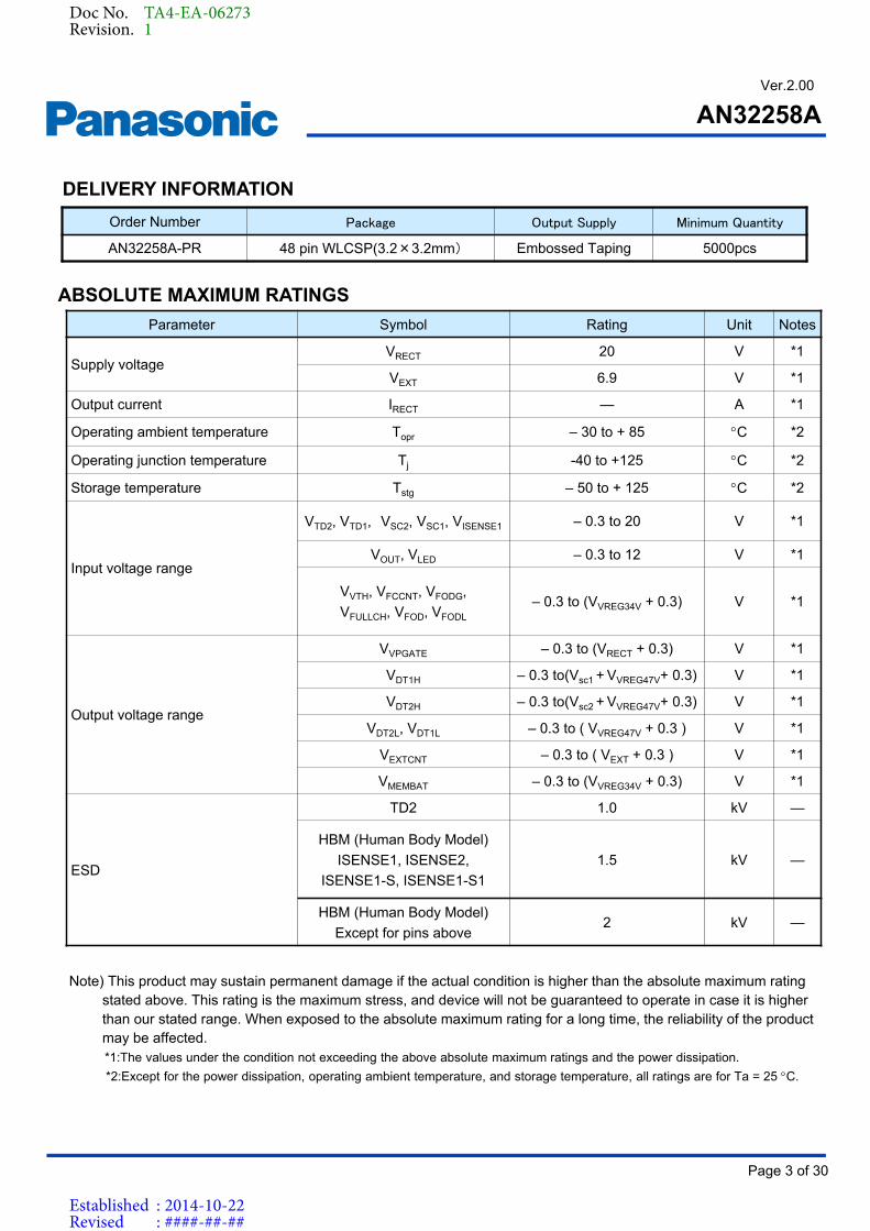
ABSOLUTE MAXIMUM RATINGS
Parameter Symbol Rating Unit Notes
Supply voltageVRECT 20 V *1
VEXT 6.9 V *1
Output current IRECT — A *1
Operating ambient temperature Topr – 30 to + 85 C *2
Operating junction temperature Tj -40 to +125 C *2
Storage temperature Tstg – 50 to + 125 C *2
Input voltage range
VTD2, VTD1, VSC2, VSC1, VISENSE1 – 0.3 to 20 V *1
VOUT, VLED – 0.3 to 12 V *1
VVTH, VFCCNT, VFODG,
VFULLCH, VFOD, VFODL
– 0.3 to (VVREG34V + 0.3) V *1
Output voltage range
VVPGATE – 0.3 to (VRECT + 0.3) V *1
VDT1H – 0.3 to(Vsc1 + VVREG47V+ 0.3) V *1
VDT2H – 0.3 to(Vsc2 + VVREG47V+ 0.3) V *1
VDT2L, VDT1L – 0.3 to ( VVREG47V + 0.3 ) V *1
VEXTCNT – 0.3 to ( VEXT + 0.3 ) V *1
VMEMBAT – 0.3 to (VVREG34V + 0.3) V *1
ESD
TD2 1.0 kV —
HBM (Human Body Model)
ISENSE1, ISENSE2,
ISENSE1-S, ISENSE1-S1
1.5 kV —
HBM (Human Body Model)
Except for pins above2 kV —
Note) This product may sustain permanent damage if the actual condition is higher than the absolute maximum rating stated above. This rating is the maximum stress, and device will not be guaranteed to operate in case it is higher than our stated range. When exposed to the absolute maximum rating for a long time, the reliability of the product may be affected.*1:The values under the condition not exceeding the above absolute maximum ratings and the power dissipation.
*2:Except for the power dissipation, operating ambient temperature, and storage temperature, all ratings are for Ta = 25 C.
Order Number Package Output Supply Minimum Quantity
AN32258A-PR 48 pin WLCSP(3.2×3.2mm) Embossed Taping 5000pcs
DELIVERY INFORMATION
Doc No. TA4-EA-06273Revision. 1
Established : 2014-10-22Revised : ####-##-##
AN32258A
Page 4 of 30
Product Standards
Ver.2.00
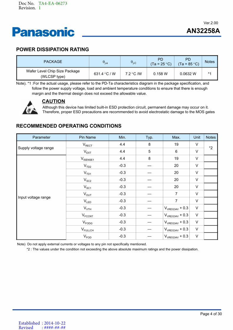
POWER DISSIPATION RATING
Note). *1 :For the actual usage, please refer to the PD-Ta characteristics diagram in the package specification, and follow the power supply voltage, load and ambient temperature conditions to ensure that there is enough margin and the thermal design does not exceed the allowable value.
CAUTIONAlthough this device has limited built-in ESD protection circuit, permanent damage may occur on it.Therefore, proper ESD precautions are recommended to avoid electrostatic damage to the MOS gates
PACKAGE j-a j-CPD
(Ta = 25 C)PD
(Ta = 85 C)Notes
Wafer Level Chip Size Package
(WLCSP type)631.4 C / W 7.2 C /W 0.158 W 0.0632 W *1
RECOMMENDED OPERATING CONDITIONS
Parameter Pin Name Min. Typ. Max. Unit Notes
Supply voltage rangeVRECT 4.4 8 19 V
*2VEXT 4.4 5 6 V
Input voltage range
VISENSE1 4.4 8 19 V
VTD2 -0.3 — 20 V
VTD1 -0.3 — 20 V
VSC2 -0.3 — 20 V
VSC1 -0.3 — 20 V
VOUT -0.3 — 7 V
VLED -0.3 — 7 V
VVTH -0.3 — VVREG34V + 0.3 V
VFCCNT -0.3 — VVREG34V + 0.3 V
VFODG -0.3 — VVREG34V + 0.3 V
VFULLCH -0.3 — VVREG34V + 0.3 V
VFOD -0.3 — VVREG34V + 0.3 V
Note) Do not apply external currents or voltages to any pin not specifically mentioned.
*2 : The values under the condition not exceeding the above absolute maximum ratings and the power dissipation.
Doc No. TA4-EA-06273Revision. 1
Established : 2014-10-22Revised : ####-##-##
AN32258A
Page 5 of 30
Product Standards
Ver.2.00
Parameter Symbol Condition Limits
Unit NoteMin Typ Max
Current Consumption
Quiescent current ISTBY 10 12 14 mA
Under-voltage lock-out (UVLO)
Under-voltage lock-out VUVLO VRECT : 0V -> 5V 3.29 3.5 3.71 V
Hysteresis on UVLO VUVLOHY VRECT : 5V -> 3V - 0.7 - V *1
Over-voltage protection (OVP)
Input overvoltage threshold VOVP VRECT : 5V -> 19V 17 18 19 V
Hysteresis on OVP VOVPOHY VRECT : 19V -> 5V - 4 - V *1
VRECT (5W, LDO 5V mode )
VRECT Threshold1 VRECTTH1
In increasing IOUT < 125mA
In decreasing I :IOUT <60mA- 8 - V *1
VRECT Threshold2 VRECTTH2
In increasing 125mA<IOUT<420mA
In decreasing 60mA<IOUT<360mA
- 5.4 - V *1
VRECT Threshold3 VRECTTH3
In increasing IOUT > 420mA
In decreasing IOUT > 360mA- 5.1 - V *1
OUTPUT
VOUT (5W, LDO 5V mode )
VOUT1 VRECT=8V ,IOUT=10mA 4.76 5 5.24 V
VOUT2
VRECT=5.1V ,
IOUT=1000mA4.76 — — V
ELECRTRICAL CHARACTERISTICSCo = 10 µF, VRECT = 8 V, Ta = 25 C 2 C unless otherwise noted.
Note) *1 : Designed typical values
Doc No. TA4-EA-06273Revision. 1
Established : 2014-10-22Revised : ####-##-##

AN32258A
Page 6 of 30
Product Standards
Ver.2.00
Parameter Symbol Condition Limits
Unit NoteMin Typ Max
Temperature Detection [Thermistor:ERTJ0EV104F]
Over-temperature Detection Voltage VTH
60 C detection
VTHR:47 kohm (1%)0.887 0.975 1.069 V
Over-current protection (OCP)
Over-current threshold voltage 1 VOCPL — 1.25 1.5 1.75 A
Thermal protection
Thermal shutdown temperature Tj — — 150 — C *1
Thermal shutdown hysteresis Tjhys — — 20 — C *1
External voltage detection
VEXT Rising threshold voltage VEXTTH — 3.99 4.2 4.41 V
VEXT hysteresis VEXTHY — — 0.4 — V *1
Terminal voltage (FULLCH)
High input threshold (Termination) VIH1 — 1.6 — — V
Low input threshold VIL1 — -0.2 — 0.2 V
Terminal voltage (FODL)
High input threshold (Termination) VIH1 — 1.6 — — V
Low input threshold VIL1 — -0.2 — 0.2 V
ELECRTRICAL CHARACTERISTICS (Continued)Co = 10 µF, VRECT = 8 V, Ta = 25 C 2 C unless otherwise noted.
Notes) *1 : Designed typical values
Doc No. TA4-EA-06273Revision. 1
Established : 2014-10-22Revised : ####-##-##

AN32258A
Page 7 of 30
Product Standards
Ver.2.00
Parameter Symbol Condition Limits
Unit NoteMin Typ
Max
LEDCNT
LED Saturation voltage LEDSAT ILED = 20mA — — 0.5 V —
LED Leak current LEDLEAK LED = 7.5V — — 10 μA —
ELECRTRICAL CHARACTERISTICS (Continued)Co = 10 µF, VRECT = 8 V, Ta = 25 C 2 C unless otherwise noted.
Doc No. TA4-EA-06273Revision. 1
Established : 2014-10-22Revised : ####-##-##
AN32258A
Page 8 of 30
Product Standards
Ver.2.00
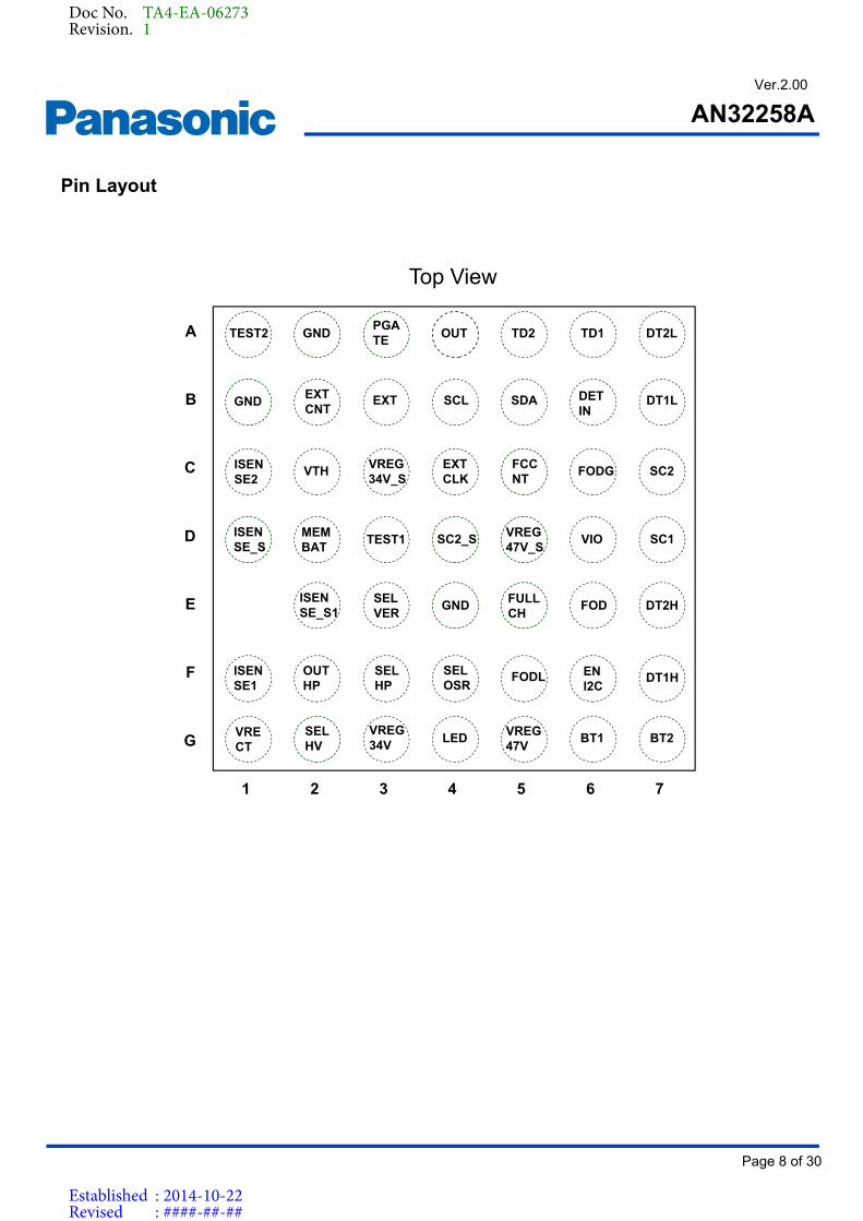
Pin Layout
Top View
VRECT
BT2SELHV
VREG34V
LEDVREG47V
BT1
ISENSE1
DT1HOUTHP
SELHP
SELOSR
FODL ENI2C
DT2HISENSE_S1
SELVER
GNDFULLCH
FOD
ISENSE_S
SC1MEMBAT
TEST1 SC2_SVREG47V_S
VIO
ISENSE2
SC2VTHVREG34V_S
EXTCLK
FCCNT
FODG
GND DT1LEXTCNT
EXT SCL SDA DETIN
TEST2 DT2LGNDPGATE
OUT TD2 TD1
1 2 3 4 5 6 7
A
G
F
E
D
C
B
Doc No. TA4-EA-06273Revision. 1
Established : 2014-10-22Revised : ####-##-##
AN32258A
Page 9 of 30
Product Standards
Ver.2.00
PIN FUNCTIONS
Pin Name I/O Function Description
A1 TEST2 I Test pinConnect to GND. Panasonic uses this pin for test purposes only.
A2,B1,E4
GND GND Ground -
A3 PGATE O LDO control Controls the PMOS gate of the LDO
A4 OUT I LDO feedbackConnects to the PMOS drain of the LDO
A5 TD2 O Drive load to transmit 2Controls capacitive load modulation for Qi data
A6 TD1 O Drive load to transmit 1Controls capacitive load modulation for Qi data
A7 DT2L O Rectification low side switch gate control 2Controls the switching gate of the low side of the rectifier
B2 EXTCNT O External PMOS control
Controls the switch to an external power supply. This pin is internally connected to the drain of NMOS to use under 2mA.When EXT is larger than 4.2V, EXTCNT will become low and the external MOSFET will turn on.
B3 EXTPower
SupplyExternal power detection
Supplies power externally in direct.When EXT becomes larger than 4.2V, EXTCNT will become low and the wireless power transmission will stop. The external power supply will then directly output, and the Tx will be stopped. (Refer to the circuit diagram followed by Pin Functions.)
B4 SCL I Test pinLeave this pin open. Panasonic uses this pin for test purposes only.
B5 SDA I/O Test pinLeave this pin open. Panasonic uses this pin for test purposes only.
B6 DETIN I Test pinLeave this pin open. Panasonic uses this pin for test purposes only.
Doc No. TA4-EA-06273Revision. 1
Established : 2014-10-22Revised : ####-##-##
AN32258A
Page 10 of 30
Product Standards
Ver.2.00
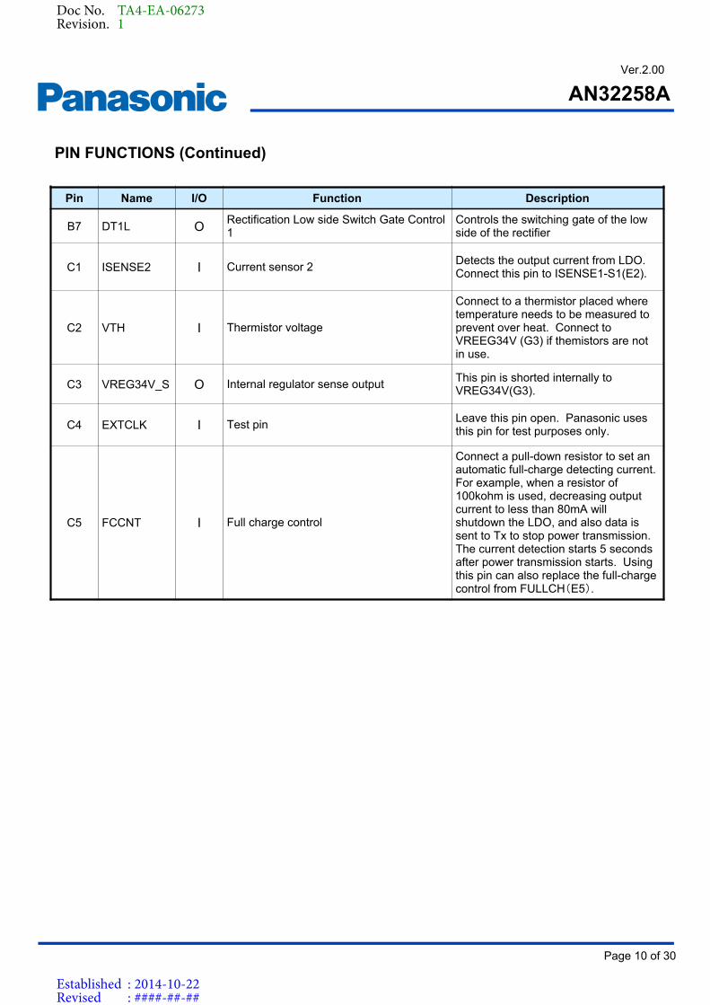
Pin Name I/O Function Description
B7 DT1L ORectification Low side Switch Gate Control 1
Controls the switching gate of the low side of the rectifier
C1 ISENSE2 I Current sensor 2Detects the output current from LDO.Connect this pin to ISENSE1-S1(E2).
C2 VTH I Thermistor voltage
Connect to a thermistor placed where temperature needs to be measured to prevent over heat. Connect to VREEG34V (G3) if themistors are not in use.
C3 VREG34V_S O Internal regulator sense outputThis pin is shorted internally to VREG34V(G3).
C4 EXTCLK I Test pinLeave this pin open. Panasonic uses this pin for test purposes only.
C5 FCCNT I Full charge control
Connect a pull-down resistor to set an automatic full-charge detecting current. For example, when a resistor of 100kohm is used, decreasing output current to less than 80mA will shutdown the LDO, and also data is sent to Tx to stop power transmission. The current detection starts 5 seconds after power transmission starts. Using this pin can also replace the full-charge control from FULLCH(E5).
PIN FUNCTIONS (Continued)
Doc No. TA4-EA-06273Revision. 1
Established : 2014-10-22Revised : ####-##-##

AN32258A
Page 11 of 30
Product Standards
Ver.2.00
Pin Name I/O Function Description
C6 FODG I FOD gain control
Connect a pull-down resistor to adjust the gain level of Received Power Packet defined in WPC specification. The resistance can be varied from 10k ohms to 180k ohms.
C7 SC2 I Synchronous rectifier control 2Connect to the rectifier to detect its voltage level.
D1 ISENSE1_S I Sense pin for ISENSE1
Connect to the source of the LDO’s MOSFET to detect the output current. A sense resistor of 50mohms is connected to ISENSE1(F1) inside the IC.
D2 MEMBAT O Random number memory adjustmentConnect a capacitor of 1uF to fix a memory time.
D3 TEST1 O Test pinLeave this pin open. Panasonic uses this pin for test purposes only.
D4 SC2_S I Synchronous rectifier sense pinLeave this pin open. Panasonic uses this pin to sense SC2(C7) for test purposes only.
D5 VREG47V_S O Internal regulator sense outputThis pin in shorted internally to VREG47V(G5).
D6 VIO I Test pinLeave this pin open. Panasonic uses this pin for test purposes only.
D7 SC1 I Synchronous rectifier control 1Connect to the rectifier to detect its voltage level.
E2 ISENSE1_S1 I Sense pin 1 for ISENSE1Connect to ISENSE2(C1) to detect the output current. Refer to the circuit diagram followed by Pin Functions.
E3 SELVER I Test pinLeave this pin open. Panasonic uses this pin for test purposes only.
PIN FUNCTIONS (Continued)
Doc No. TA4-EA-06273Revision. 1
Established : 2014-10-22Revised : ####-##-##

AN32258A
Page 12 of 30
Product Standards
Ver.2.00
Pin Name I/O Function Description
E5 FULLCH I Full charge detection
This input controls the full charge detection externally such as from an MCU. When a high voltage level (over 1.6V) is inputted for over 50us, AN32258A will recognize it as full-charge and send packets to Tx to stop the power transmission. Right after the input becomes low, the power transmission can restart.
E6 FOD O Foreign object detection offset
Connect a pull-down resistor to adjust the offset level of received power of WPC specification. For example, a pull-down resistor of 100kohm will set the offset to be zero. Refer to No.3 of the Functions section.
E7 DT2H ORectification high side switch gate control 2
Controls the switching gate of the high side of the rectifier
F1 ISENSE1 I Current sensor 1
Connect to VRECT(G1) to detect the output current. A sense resistor of 50mohms is connected to ISENSE1-S(D1) inside the IC.
F2 OUTHP O TEST pinLeave this pin open. Panasonic uses this pin for test purposes only.
F3 SELHP I TEST pinConnect to GND. Panasonic uses this pin for test purposes only.
F4 SELOSR I TEST pinConnect to GND. Panasonic uses this pin for test purposes only.
PIN FUNCTIONS (Continued)
Doc No. TA4-EA-06273Revision. 1
Established : 2014-10-22Revised : ####-##-##
AN32258A
Page 13 of 30
Product Standards
Ver.2.00
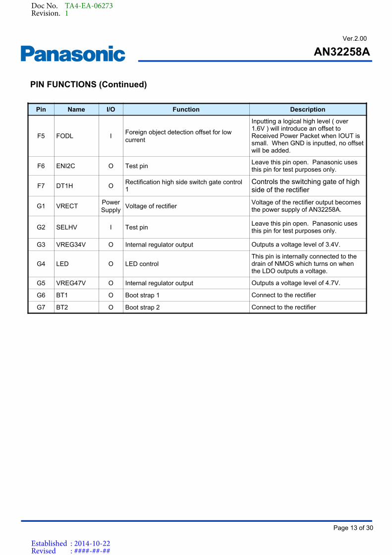
Pin Name I/O Function Description
F5 FODL IForeign object detection offset for low current
Inputting a logical high level ( over 1.6V ) will introduce an offset to Received Power Packet when IOUT is small. When GND is inputted, no offset will be added.
F6 ENI2C O Test pinLeave this pin open. Panasonic uses this pin for test purposes only.
F7 DT1H ORectification high side switch gate control 1
Controls the switching gate of high side of the rectifier
G1 VRECTPower Supply
Voltage of rectifierVoltage of the rectifier output becomes the power supply of AN32258A.
G2 SELHV I Test pinLeave this pin open. Panasonic uses this pin for test purposes only.
G3 VREG34V O Internal regulator output Outputs a voltage level of 3.4V.
G4 LED O LED controlThis pin is internally connected to the drain of NMOS which turns on when the LDO outputs a voltage.
G5 VREG47V O Internal regulator output Outputs a voltage level of 4.7V.
G6 BT1 O Boot strap 1 Connect to the rectifier
G7 BT2 O Boot strap 2 Connect to the rectifier
PIN FUNCTIONS (Continued)
Doc No. TA4-EA-06273Revision. 1
Established : 2014-10-22Revised : ####-##-##
AN32258A
Page 14 of 30
Product Standards
Ver.2.00
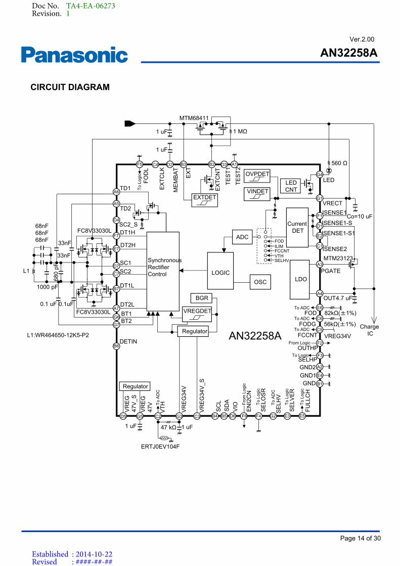
CIRCUIT DIAGRAM
BT1
TD2
TD1
BT2
VRECT
Charge IC
OUT
PGATE
VR
EG
34V
DT1H
DT2H
DT1L
DT2L
SC1
SC2
SynchronousRectifierControl
LDOLOGIC
EXTDET
LEDCNT
LED
EX
TC
NT
VINDET
SC
L
VIO
SD
A
ADC
OSC
ISENSE2
ME
MB
AT
VR
EG
47V
Regulator
FU
LLC
H
VT
H
SE
LHV
DETIN
VREGDET
BGR
Regulator
TE
ST
2
FOD
SE
LOS
R
68nF68nF68nF
0.1 uF 0.1uF
33nF
33nF
ERTJ0EV104F
AN32258A
1000 pF
A6
A5
F7
E7
D7
C7
B7
A7
G6
G7
G5D5
VR
EG
47V
_S
VR
EG
34V
_S
C2 G3 C3 B4 B5 D6
FODG
FCCNT
FODILIMFCCNTVTHSELHV
E6
C6
C5
G2
To
AD
C
To ADC
To ADC
To ADC
To
AD
C
F4
A4
OVPDET
To
Logi
c
SE
LVE
R
E3
D2
A3
C1
ISENSE1-S1E2
ISENSE1-SD1
ISENSE1F1
G1
G4
E5
To
Logi
c
To
Logi
c
C4E
XT
CLK
D4SC2_S
EX
T
B3F5
FO
DL
To
Logi
c
OUTHPF2From Logic
F6
EN
I2C
NF
rom
Log
ic
1 uF
A2
E4
B1
GND2
GND1GND
TE
ST
1
D3 A1
1 uF 1 uF47 kΩ
4.7 uF
Co=10 uF
560 Ω
SELHPF3To Logic
VREG34V
82kΩ(±1%)
56kΩ(±1%)
Current DETFC8V33030L
MTM23123
L1
FC8V33030L
680
pF
B6
B2
1 MΩ
MTM68411
1 uF
L1:WR464650-12K5-P2
Doc No. TA4-EA-06273Revision. 1
Established : 2014-10-22Revised : ####-##-##
AN32258A
Page 15 of 30
Product Standards
Ver.2.00
FUNCTIONS
AN32258A has the following functions.
No. Function
1 Full charge control
2 Over current control
3 Foreign object detection
4 Over temperature detection
5 Rectifier voltage control
6 LED display
7 External voltage supply switch
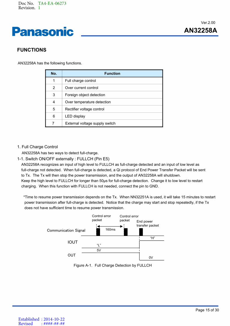
1. Full Charge Control
AN32258A has two ways to detect full-charge.
1-1. Switch ON/OFF externally : FULLCH (Pin E5)AN32258A recognizes an input of high level to FULLCH as full-charge detected and an input of low level as
full-charge not detected. When full-charge is detected, a Qi protocol of End Power Transfer Packet will be sent
to Tx. The Tx will then stop the power transmission, and the output of AN32258A will shutdown.
Keep the high level to FULLCH for longer than 50μs for full-charge detection. Change it to low level to restart
charging. When this function with FULLCH is not needed, connect the pin to GND.
*Time to resume power transmission depends on the Tx. When NN32251A is used, it will take 15 minutes to restart
power transmission after full-charge is detected. Notice that the charge may start and stop repeatedly, if the Tx
does not have sufficient time to resume power transmission.
“L”
“H”
5V
0V
160ms
Control error packet End power
transfer packet
Control error packet
Communication Signal
IOUT
OUT
Figure A-1. Full Charge Detection by FULLCH
Doc No. TA4-EA-06273Revision. 1
Established : 2014-10-22Revised : ####-##-##

AN32258A
Page 16 of 30
Product Standards
Ver.2.00
FUNCTIONS (Continued)
1-2. Control by output current: FCCNT (Pin C5)When charging current becomes less than the value set at FCCNT (Pin C5), the power transmission
stops as full charge. The threshold is determined by a pull-down resistor connected at this pin.
For example, when a resistor of 100kohm is used, decreasing output current to less than 80mA will shutdown
the LDO, and also data is sent to Tx to stop power transmission. The data to transmit is defined in Qi and
called End Power Transfer packet. The current detection starts 5 seconds after power transmission starts.
Connect this pin to VREG34V, when this full-charge detection is not needed. When FULLCH pin is
connected to high level to be activated, FCCNT will not control the full-charge detection. This function does
not work for FCCNT voltage of over 3V. Also, note that the minimum threshold is 40mA.
*Time to resume power transmission depends on the Tx. When NN32251A is used, it will take 15 minutes to restart
power transmission after full-charge is detected. Notice that the charge may start and stop repeatedly, if the Tx
does not have sufficient time to resume power transmission.
resistance [kohm](FCCNT [V])
Ful
l-cha
rge
Cur
rent
[mA
]
100 (0.136)
80
735 (1.0)
588
-(>3V)
Communication Signal
IOUT
OUT
Full-charge current5V
0V
160ms
Control error packet End power
transfer packet
Control error packet
Detected at the timing of a control error packet by an AD converter
160ms
Control error packet
FigureA-3. Full charge detecting current is controlled by a resistor connected to FCCNT.
Full-charge Current [mA] = 2000/3.4 x 0.00000136 x R[Ω]
Figure A-2. Full Charge Detection by FCCNT
Doc No. TA4-EA-06273Revision. 1
Established : 2014-10-22Revised : ####-##-##

AN32258A
Page 17 of 30
Product Standards
Ver.2.00
2.Current Limit ControlWhen the output current exceeds the threshold value, AN32258A will shutdown the output.
. When this over-current is detected, data is sent to Tx to stop power transmission. The data to transmit to Tx is
End Power Transfer packet defined in Qi, and right after the Tx receives the data, it stops its power transmission.
The threshold value is about 1.5A.
FUNCTIONS (Continued)
Figure A-4. Timing characteristics for current limit control
Communication Signal
IOUT
OUT
1.5A
5V
0V
160ms
Control error packet End power
transfer packet
Control error packet
3.Foreign Object DetectionAN32258A has a foreign object detection complying with the WPC 1.1 specification. The specification defines a
foreign object when the difference between transmitted power and received power is large. The Tx measures
the power difference and stops power transmission when the difference is large.
The value of Received Power (address 04h) can be adjusted by the following three pins.
3-1. Offset Control :FOD (Pin E6)
Connect a pull-down resistor at FOD pin to adjust the offset level of received power sent to the Tx.
For example, a pull-down resistor of 100kohm will set the offset to be zero. This function does not work
for FOD voltage of over 3V.
If this function is not needed, connect the FOD pin to VREG34V.
FO
D o
ffset
[mW
]
35.3 (0.6)
-400
100 (1.7)
0
(>3V)165 (2.8)
+400
Figure A-5. FOD offset is controlled by a resistor connected to FOD pin
Resistance Value [kohm](FOD [V])
Doc No. TA4-EA-06273Revision. 1
Established : 2014-10-22Revised : ####-##-##
AN32258A
Page 18 of 30
Product Standards
Ver.2.00
3.Foreign Object Detection (Continued)3-2. Offset Control for low current :FOD (Pin F5)
An offset can be introduced to the received power for low current at IOUT.
Set the FODL pin to either logical high or low.
Low (GND) : No offset
High (over 1.6V) : Offset added (IOUT < ~125mA)
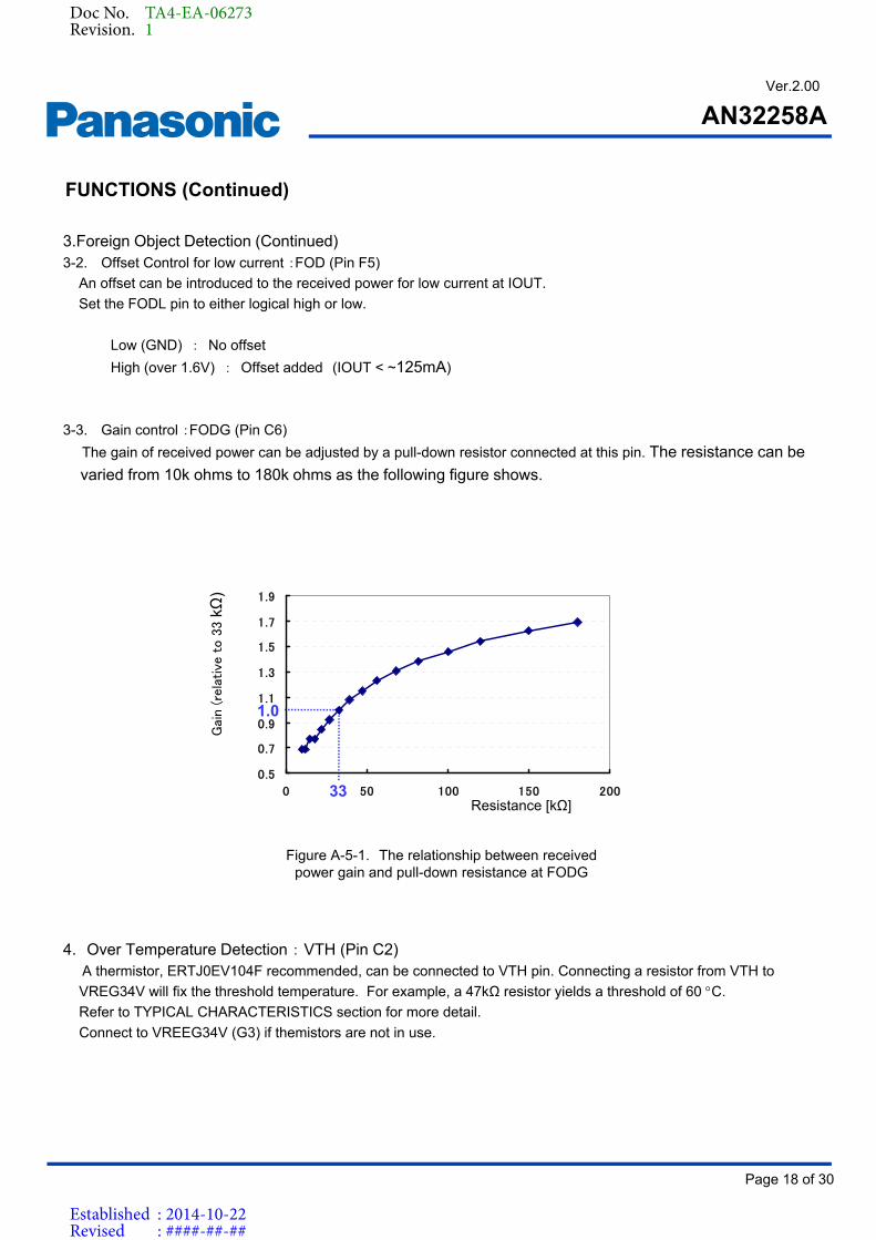
3-3. Gain control :FODG (Pin C6)
The gain of received power can be adjusted by a pull-down resistor connected at this pin. The resistance can be
varied from 10k ohms to 180k ohms as the following figure shows.
0.5
0.7
0.9
1.1
1.3
1.5
1.7
1.9
0 50 100 150 20033Resistance [kΩ]
1.0
Figure A-5-1. The relationship between received power gain and pull-down resistance at FODG
FUNCTIONS (Continued)G
ain (re
lative
to 3
3 kΩ
)
4. Over Temperature Detection : VTH (Pin C2)A thermistor, ERTJ0EV104F recommended, can be connected to VTH pin. Connecting a resistor from VTH to
VREG34V will fix the threshold temperature. For example, a 47kΩ resistor yields a threshold of 60 C.
Refer to TYPICAL CHARACTERISTICS section for more detail.
Connect to VREEG34V (G3) if themistors are not in use.
Doc No. TA4-EA-06273Revision. 1
Established : 2014-10-22Revised : ####-##-##

AN32258A
Page 19 of 30
Product Standards
Ver.2.00
5. Rectifier Voltage ControlAN32258A controls the rectifier output (VRECT) depending on the current value (IOUT). The following figure
shows the change of VRECT due to IOUT. Note that the changed timing in increasing IOUT is different
from that in decreasing IOUT.
VRECT
125mA0mA
1000mA
8 V
5.1 V
420mA
5.4 V
60mA
380mA
5.4 V
8 V
0mAIOUT
FUNCTIONS (Continued)
Figure A-8. VRECT changes by the value of output current.(Values shown are for reference.)
Doc No. TA4-EA-06273Revision. 1
Established : 2014-10-22Revised : ####-##-##
AN32258A
Page 20 of 30
Product Standards
Ver.2.00
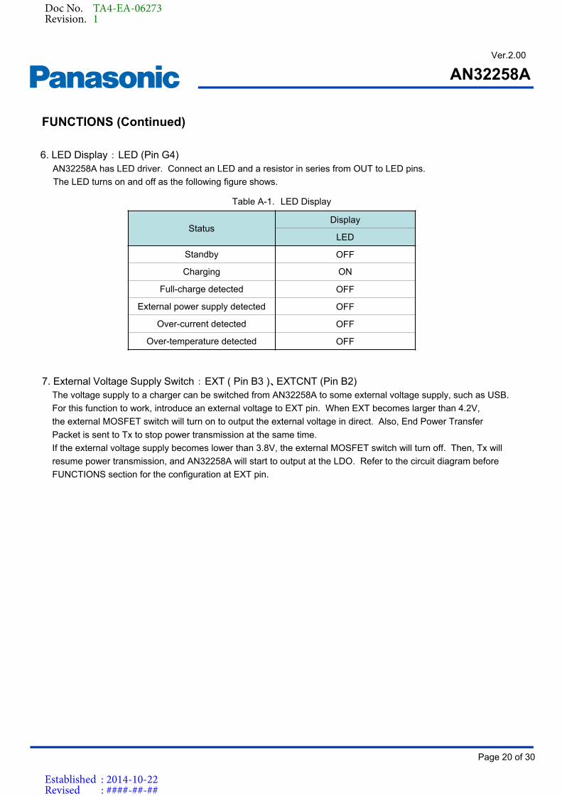
6. LED Display : LED (Pin G4)AN32258A has LED driver. Connect an LED and a resistor in series from OUT to LED pins.
The LED turns on and off as the following figure shows.
StatusDisplay
LED
Standby OFF
Charging ON
Full-charge detected OFF
External power supply detected OFF
Over-current detected OFF
Over-temperature detected OFF
7. External Voltage Supply Switch : EXT ( Pin B3 )、EXTCNT (Pin B2)The voltage supply to a charger can be switched from AN32258A to some external voltage supply, such as USB.
For this function to work, introduce an external voltage to EXT pin. When EXT becomes larger than 4.2V,
the external MOSFET switch will turn on to output the external voltage in direct. Also, End Power Transfer
Packet is sent to Tx to stop power transmission at the same time.
If the external voltage supply becomes lower than 3.8V, the external MOSFET switch will turn off. Then, Tx will
resume power transmission, and AN32258A will start to output at the LDO. Refer to the circuit diagram before
FUNCTIONS section for the configuration at EXT pin.
FUNCTIONS (Continued)
Table A-1. LED Display
Doc No. TA4-EA-06273Revision. 1
Established : 2014-10-22Revised : ####-##-##
AN32258A
Page 21 of 30
Product Standards
Ver.2.00
EVALUATION RESULTS
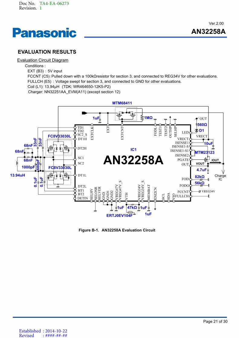
Figure B-1. AN32258A Evaluation Circuit
Evaluation Circuit Diagram
BT1
TD2TD1
BT2
GND2
VRECTVREG34V
DT1H
DT2H
DT1L
DT2L
SC1
SC2
ISENSE1
MEMBAT
VREG47V
68nF
68nF
1000pF
33n
F33
nF
FC8V33030L
AN32258AIC1
EXT
EXTCNT
MTM68411
1MΩ1uF OUT
LED
560Ω
D1VTH
SELOSR
FULLCH
Charge IC
OUTPGATEISENSE2
4.7uF
MTM23123
82kΩFOD
FODG
FCCNT
ISENSE1-S1
TEST2
10uF68nF ISENSE1-S
VREG34V
EXTCLK
FODL
TEST1
OUTHP
SELHP
GND1
GND
SELVER
SELHV
VREG47V_S
VREG34V_S
DETIN
SC2_S
ENI2CN
SCL
SDA
VIO
56kΩ
ERTJ0EV104F
47kΩ
1uF
1uF1uF
0.1u
F
0.1u
F
FC8V33030L
VRECT
IOUTVOUT
680p
F
13.94uH
Conditions : EXT (B3) : 5V inputFCCNT (C5):Pulled down with a 100kΩresistor for section 3, and connected to REG34V for other evaluations.FULLCH (E5) : Voltage swept for section 3, and connected to GND for other evaluations.Coil (L1): 13.94μH (TDK: WR464650-12K5-P2)Charger: NN32251AA_EVM(A11) (except section 12)
Doc No. TA4-EA-06273Revision. 1
Established : 2014-10-22Revised : ####-##-##

AN32258A
Page 22 of 30
Product Standards
Ver.2.00
1.Output Voltage Characteristics 2. VRECT Voltage Characteristics
IOUT [A]V
RE
CT
V]
Figure B-2 Output Voltage vs Output Current Figure B-3 VRECT Voltage vs Output Current
VO
UT
[V
]
IOUT [A]
0
0.2
0.4
0.6
0.8
1
1.2
1.4
1.6
0 0.5 1 1.5 2 2.5 3
IOU
T [A
]
FCCNT [V]
0
1
2
3
4
5
6
0 0.2 0.4 0.6 0.8 1
VO
UT
[V
]
FULLCH [V]
3. Full-Charge Characteristics
Figure B-4 Full-Charge Detecting Current vs FCCNT Voltage with a 100kΩResistor Connected
Figure B-5 Output Voltage vs FULLCH Level
Figure B-6 Received Signal Characteristics after a Full-Charge Detection
*After the output voltage becomes zero, an End Power Transfer Packet is sent.
TYPICAL CHARACTERISTICS (Continued)
VRECT
OUTTD
1
VRECTOUT TD1
Doc No. TA4-EA-06273Revision. 1
Established : 2014-10-22Revised : ####-##-##

AN32258A
Page 23 of 30
Product Standards
Ver.2.00
4. Over Current Protection Characteristics
Figure B-7 VOUT vs IOUT
5. Temperature Detection Characteristics
0
1
2
3
4
5
6
0 0.5 1 1.5 2 2.5
VO
UT
[V
]
IOUT [A]
VO
UT
[V
]
VTH [V]
Figure B-8 Output Voltage vs VTHFigure B-9 Received Signal Characteristics after a Temperature Detection
*Conditions : IOUT =500mA
The power transmission from Tx stops due to
temperature detection (VTH).
TYPICAL CHARACTERISTICS (Continued)
VRECT
TD1OUT
Doc No. TA4-EA-06273Revision. 1
Established : 2014-10-22Revised : ####-##-##

AN32258A
Page 24 of 30
Product Standards
Ver.2.00
6. Over Voltage Protection Characteristics
0
1
2
3
4
5
6
5 7 9 11 13 15 17 19 21
Figure B-10 VOUT vs VRECT by OVP
VO
UT
[V
]
VRECT [V]
Figure B-11 Output Voltage Response by OVP7. Foreign Object Detection Characteristics
Rec
eive
d P
ower
[W
]
FOD [V]
0
1
2
3
4
5
6
7
8
0 1 2 3
Iout=0.1A
Iout=0.2A
Iout=0.3A
Iout=0.4A
Iout=0.5A
Iout=0.6A
Iout=0.7A
Iout=0.8A
Iout=0.9A
Iout=1.0A
*Received Power = (RPWR[7:0] / 128) × (Maximum Power / 2) ×10Power Class W
TYPICAL CHARACTERISTICS (Continued)
Figure B-12 Received Power vs FOD Voltage
VRECT
OUT
VRECT
OUT
18V
14V
Doc No. TA4-EA-06273Revision. 1
Established : 2014-10-22Revised : ####-##-##

AN32258A
Page 25 of 30
Product Standards
Ver.2.00
8. External Power Supply Switch Characteristics
9. Start-up Characteristics
Figure B-13 Voltage when an External Power is Inputted during Normal Wireless Power Transmission
Figure B-16 Rx Communication Packet Structure
10. Communication Packet Configuration
PREAMBLE HEADER MESSAGE CHECKSUM
0 0 1 0 0 0 0 0STRAT
PARITY STOP
TYPICAL CHARACTERISTICS (Continued)
*Condition : IOUT=1000mA
*Condition : IOUT=500mA
Figure B-14 Normal Power Transmission Resumes after the External Power Turns Off.
*Condition : IOUT=500mA
Figure B-15 Characteristics of Starting Wireless Power Transmission
VRECT
EXTCNTEXT
EXT=5V印加
OUT
VRECT
EXTCNT
EXT
OUT
EXT=5V OFF
VRECT
IOUT
OUT
Doc No. TA4-EA-06273Revision. 1
Established : 2014-10-22Revised : ####-##-##

AN32258A
Page 26 of 30
Product Standards
Ver.2.00
VRECT
LED
OUTIOUT
VRECT
LED
OUT
VRECT
VTHLED
OUT
VRECT
VREG34V
LED
OUT
VRECT
LED
OUT
11. LED Display Characteristics
FULLCH:Low→High VTH:High→Low
Over current detected
TYPICAL CHARACTERISTICS (Continued)
Figure B-19 LED Turned off by a Full Charge
Figure B-17 LED Characteristics 1*Condition : LED is pulled up to VREG34V first
Figure B-18 LED Characteristics 2*LED lights up when the output starts.
Figure B-20 LED Turned off by an over temperature
*VTH detects an over temperature, and LED turns off when the output goes down.
*FULLCH detects a full-charge, and LED turns off when the output goes down.
Figure B-21 LED Turned off by an over currentAfter an over current is detected, LED turns off when the output goes down.
LED-pin Low LED turns on
Doc No. TA4-EA-06273Revision. 1
Established : 2014-10-22Revised : ####-##-##
AN32258A
Page 27 of 30
Product Standards
Ver.2.00
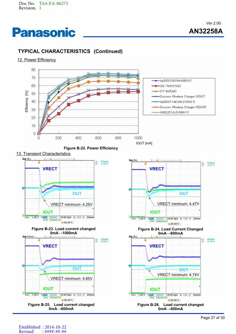
12. Power Efficiency
Figure B-22. Power Efficiency
13. Transient Characteristics
Effi
cien
cy
[%]
IOUT [mA]
Figure B-23. Load current changed 0mA→1000mA
Figure B-24. Load Current Changed 0mA→800mA
Figure B-25. Load current changed0mA→600mA
Figure B-26. Load current changed 0mA→400mA
TYPICAL CHARACTERISTICS (Continued)
VRECT minimum: 4.25V VRECT minimum: 4.47V
OUT
IOUT
VRECT
OUT
IOUT
VRECT
VRECT minimum: 4.74VVRECT minimum: 4.65V
OUT
IOUT
VRECT
OUT
IOUT
VRECT
Doc No. TA4-EA-06273Revision. 1
Established : 2014-10-22Revised : ####-##-##
AN32258A
Page 28 of 30
Product Standards
Ver.2.00
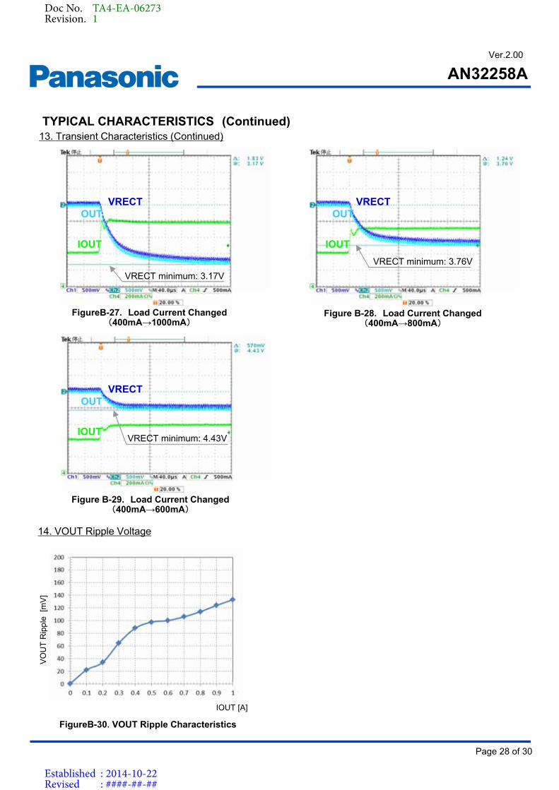
14. VOUT Ripple Voltage
IOUT [A]
VO
UT
Rip
ple
[m
V]
FigureB-30. VOUT Ripple Characteristics
FigureB-27. Load Current Changed(400mA→1000mA)
Figure B-28. Load Current Changed(400mA→800mA)
Figure B-29. Load Current Changed(400mA→600mA)
TYPICAL CHARACTERISTICS (Continued)13. Transient Characteristics (Continued)
OUT
IOUT
VRECT
VRECT minimum: 3.17V
VRECT minimum: 3.76V
OUT
IOUT
VRECT
VRECT minimum: 4.43V
OUT
IOUT
VRECT
Doc No. TA4-EA-06273Revision. 1
Established : 2014-10-22Revised : ####-##-##

AN32258A
Page 29 of 30
Product Standards
Ver.2.00
Package Information
Package Code : XBGA048-W-3232AMLUnit: mm
Doc No. TA4-EA-06273Revision. 1
Established : 2014-10-22Revised : ####-##-##

AN32258A
Page 30 of 30
Product Standards
Ver.2.00
IMPORTANT NOTICE
1. When using the IC for new models, verify the safety including the long-term reliability for each product.
2. When the application system is designed by using this IC, please confirm the notes in this book. Please read the notes to descriptions and the usage notes in the book.
3. This IC is intended to be used for general electronic equipment.Consult our sales staff in advance for information on the following applications: Special applications in which exceptional quality and reliability are required, or if the failure or malfunction of this IC may directly jeopardize life or harm the human body.Any applications other than the standard applications intended.
(1) Space appliance (such as artificial satellite, and rocket)(2) Traffic control equipment (such as for automotive, airplane, train, and ship)(3) Medical equipment for life support(4) Submarine transponder(5) Control equipment for power plant(6) Disaster prevention and security device(7) Weapon(8) Others : Applications of which reliability equivalent to (1) to (7) is required
Our company shall not be held responsible for any damage incurred as a result of or in connection with the IC being used for any special application, unless our company agrees to the use of such special application.However, for the IC which we designate as products for automotive use, it is possible to be used for automotive.
4. This IC is neither designed nor intended for use in automotive applications or environments unless the IC is designated by our company to be used in automotive applications.
Our company shall not be held responsible for any damage incurred by customers or any third party as a result of or in connection with the IC being used in automotive application, unless our company agrees to such application in this book.
5. Please use this IC in compliance with all applicable laws and regulations that regulate the inclusion or use of controlled substances, including without limitation, the EU RoHS Directive. Our company shall not be held responsible for any damage incurred as a result of our IC being used by our customers, not complying with the applicable laws and regulations.
6. Pay attention to the direction of the IC. When mounting it in the wrong direction onto the PCB (printed-circuit-board), it might be damaged.
7. Pay attention in the PCB (printed-circuit-board) pattern layout in order to prevent damage due to short circuit between pins. In addition, refer to the Pin Description for the pin configuration.
8. Perform visual inspection on the PCB before applying power, otherwise damage might happen due to problems such as solder-bridge between the pins of the IC. Also, perform full technical verification on the assembly quality, because the same damage possibly can happen due to conductive substances, such as solder ball, that adhere to the IC during transportation.
9. Take notice in the use of this IC that it might be damaged when an abnormal state occurs such as output pin-VCC short (Power supply fault), output pin-GND short (Ground fault), or output-to-output-pin short (load short). Safety measures such as installation of fuses are recommended because the extent of the above-mentioned damage will depend on the current capability of the power supply.
10. The protection circuit is for maintaining safety against abnormal operation. Therefore, the protection circuit should not work during normal operation.Especially for the thermal protection circuit, if the area of safe operation or the absolute maximum rating is momentarily exceeded due to output pin to VCC short (Power supply fault), or output pin to GND short (Ground fault), the IC might be damaged before the thermal protection circuit could operate.
11. Unless specified in the product specifications, make sure that negative voltage or excessive voltage are not applied to the pins because the IC might be damaged, which could happen due to negative voltage or excessive voltage generated during the ON and OFF timing when the inductive load of a motor coil or actuator coils of optical pick-up is being driven.
12. Verify the risks which might be caused by the malfunctions of external components.
Doc No. TA4-EA-06273Revision. 1
Established : 2014-10-22Revised : ####-##-##

Request for your special attention and precautions in using the technical information andsemiconductors described in this book
(1) If any of the products or technical information described in this book is to be exported or provided to non-residents, the laws and regulations of the exporting country, especially, those with regard to security export control, must be observed.
(2) The technical information described in this book is intended only to show the main characteristics and application circuit examples of the products. No license is granted in and to any intellectual property right or other right owned by Panasonic Corporation or any other company. Therefore, no responsibility is assumed by our company as to the infringement upon any such right owned by any other company which may arise as a result of the use of technical information described in this book.
(3) The products described in this book are intended to be used for general applications (such as office equipment, communications equipment, measuring instruments and household appliances), or for specific applications as expressly stated in this book.Consult our sales staff in advance for information on the following applications: Special applications (such as for airplanes, aerospace, automotive equipment, traffic signaling equipment, combustion equipment,
life support systems and safety devices) in which exceptional quality and reliability are required, or if the failure or malfunction of the products may directly jeopardize life or harm the human body.
It is to be understood that our company shall not be held responsible for any damage incurred as a result of or in connection with your using the products described in this book for any special application, unless our company agrees to your using the products in this book for any special application.
(4) The products and product specifications described in this book are subject to change without notice for modification and/or im-provement. At the final stage of your design, purchasing, or use of the products, therefore, ask for the most up-to-date Product Standards in advance to make sure that the latest specifications satisfy your requirements.
(5) When designing your equipment, comply with the range of absolute maximum rating and the guaranteed operating conditions (operating power supply voltage and operating environment etc.). Especially, please be careful not to exceed the range of absolute maximum rating on the transient state, such as power-on, power-off and mode-switching. Otherwise, we will not be liable for any defect which may arise later in your equipment.
Even when the products are used within the guaranteed values, take into the consideration of incidence of break down and failure mode, possible to occur to semiconductor products. Measures on the systems such as redundant design, arresting the spread of fire or preventing glitch are recommended in order to prevent physical injury, fire, social damages, for example, by using the products.
(6) Comply with the instructions for use in order to prevent breakdown and characteristics change due to external factors (ESD, EOS, thermal stress and mechanical stress) at the time of handling, mounting or at customer's process. When using products for which damp-proof packing is required, satisfy the conditions, such as shelf life and the elapsed time since first opening the packages.
(7) This book may be not reprinted or reproduced whether wholly or partially, without the prior written permission of our company.
20100202