Embed Size (px)
Citation preview

Application ReportSLUA724–August 2014
Test and Troubleshoot a Wireless Power Receiver
TaharAllag
ABSTRACTTesting and troubleshooting a wireless power system sometimes is challenging and may take a lot of time.The following application note provides techniques and tricks on how to troubleshoot wireless powerrelated issues and the correct method of testing them.
Contents1 Selecting the Right Device and Component for the Right Application ............................................... 2
1.1 Troubleshooting Step by Step..................................................................................... 32 Efficiency Check ............................................................................................................. 7
2.1 How to Measure AC/DC Efficiency ............................................................................... 73 Thermal Issues............................................................................................................... 94 Foreign Object Detection (FOD) Check................................................................................... 9
List of Figures
1 Good Start-Up Sequence Using the bq51020 ........................................................................... 32 Good Start Up Sequence in PMA ......................................................................................... 43 Modulation Depth in PMA System......................................................................................... 54 POUT Measurement ........................................................................................................... 75 AC Input Power Measurements ........................................................................................... 8
1SLUA724–August 2014 Test and Troubleshoot a Wireless Power ReceiverSubmit Documentation Feedback
Copyright © 2014, Texas Instruments Incorporated

Selecting the Right Device and Component for the Right Application www.ti.com
1 Selecting the Right Device and Component for the Right ApplicationThe right selection of the device, coil, PCB, and components of any application is the first and the mostimportant step in the design cycle of a wireless power system. Any wrong selection of these parts canaffect the overall performance of the whole system. For example, selecting the coil inductance value for a5-W/5-V application affects the overall DC/DC efficiency and thermal performance of the system. Shieldingmaterial can significantly affect thermal performance of the receiver, foreign detection of the board, andcoupling between the primary and secondary coils. Also, the voltage rating of the components is critical.For example, using a 10 V voltage rating on the resonant capacitors that are connected to AC pins thatcan go as high as 15 V is a critical mistake. This degrades the lifetime of the capacitor and causes amalfunction of the receiver.
Here are some steps that help to successfully design a wireless power receiver:1. Use the Texas Instrument’s evaluation board as a reference without including all the jumpers and the
test points that are used for evaluation purposes only.2. Do the same with the layout; follow the evaluation board as much as possible. Use the receiver layout
guidelines application notes from the TI website.3. Design RILIM and RTERM for the needed current limit and termination level according to the data
sheet equations.4. Design the status pins, as needed, such as WPG, CHG, PD_DET and so forth. Use the appropriate
datasheet for more information on the behavior of these pins.5. Design the TS pin according to the datasheet and RNTC used. Help is available using the calculation
tools provided on the TI website.6. Start with the default resonant caps in the EVM (Cs and Cd), then tune with the final configuration of
the board and the selected coil and shielding, according to WPC.7. Use the right voltage rating for the Cs, Cd, CRECT, CCOMM, CBOOT, CCLAMP, and COUT. The voltage ratings
are provided in the EVM user’s guide and/or the datasheet.8. Use good tolerance resistors as recommended by the user guide of the corresponding evaluation
board.9. Initially use the default values from the EVM as starting RFOD and ROS values. After building the
board, these values need to be tuned according to WPC requirement for foreign object detection(FOD).
10. It is always a good idea to use two place holders in series for RFOD and ROS on the initial layout(RFOD is highly recommended). This should provide more flexibility to use non-standard values afterFOD calibration is performed. Contact the TI sales office for details regarding the FOD calibrationprocess.
11. The TI RX EVM user's guides generally provide a list of verified coils for that EVM. This is usually agood place to start for coil selection. For example, the bq51013BEVM-764 shows 3 coils that havebeen verified as functional. Note that many other coils can be used as well. For additional information,investigations can be done into different inductor wire types (single wire, bifilar, and Litz wire). Theshape and physical size of the selected coil may need to be chosen based on the end-applicationrequirements. Some applications may benefit from a coil made into a PCB – these tend to be lessefficient but can offer other benefits.
12. Always remember that metals surrounding the secondary coil can affect the coupling, efficiency, FODand the overall performance of the system.
13. A layout guidelines application report (SLUA710) is published on the web (www.ti.com/wirelesspower);follow the instructions for best performance and good layout design.
2 Test and Troubleshoot a Wireless Power Receiver SLUA724–August 2014Submit Documentation Feedback
Copyright © 2014, Texas Instruments Incorporated

www.ti.com Selecting the Right Device and Component for the Right Application
1.1 Troubleshooting Step by StepTroubleshooting the RX with a known good TX, what to look for on the RX?
1.1.1 Steps During Start Up1. Place RX on TX in WPC—analog ping from TX changes by at least 10%, signaling that a receiver is on
the charging pad.2. Now use digital ping to identify—digital ping is a 70-ms pulse at 175 kHz.3. This powers up the RX. It sends out signal strength packet, identification packet, and configuration
packet.4. RX to TX communications are good—TX moves to power transfer phase.5. VRECT voltage must be between approximately 7 V to 8 V to enable 5-V internal LDO– The RX will send
Control Error packets to tune TX operating point to generate approximately 8 V at Vrect. See Figure 1for an example of start up on the bq51020 receiver.
6. 5-V LDO output enabled—once VRECT has reached approximately 8 V, the LDO is enabled and voltageis applied to the load. VRECT will drop but should stay above LDO drop out of 5.1 V to 5.2 V, dependingon the load and current limit.
7. RX then sends Control Error Packets (EPT) to tune the operating point to match load.
Figure 1. Good Start-Up Sequence Using the bq51020
8. In a PMA system, the startup sequence is different from WPC.9. The rectification voltage comes up immediately after the digital pings from the PMA Type 1 transmitter.10. Next is the stabilization period, then RXID message, with the Guard Time following after.11. The Guard Time is used to give some time to the PMA Type 1 TX to calculate CRC and validate the
received RXID.12. The required start up time for PMA Type 1 TX should be less than 1 second. It should be measured
from the first digital ping to the time VOUT opens up.
3SLUA724–August 2014 Test and Troubleshoot a Wireless Power ReceiverSubmit Documentation Feedback
Copyright © 2014, Texas Instruments Incorporated
Selecting the Right Device and Component for the Right Application www.ti.com
Figure 2. Good Start Up Sequence in PMA
1.1.2 Troubleshooting After Start Up• Ripple on the output voltage:
– Increase the output and/or the RECT cap, this helps absorb some ripples.– Reduce the output trace length; this reduces picking up noise, voltage drops, and parasitic
inductance issues.– Input cap of the upstream charger, make sure they are designed properly—the cap value, the
voltage rating of the cap, and layout (distance from the pin of the IC) need to be designed properly.– Sometimes the ripple at the output voltage is caused by the communication current limit feature of
the receiver IC. If this feature is enabled, it limits the current to a certain level duringcommunication. Thus, the output voltage drops to VIN-DPM of the charger. If this behavior is notdesired, disable the communication limit feature of the receiver. The communication current limit isuseful for noisy load systems and helps robust communication.
• Bad load transients– Make sure to have a VIN-DPM of the battery charger– Use LPRB in the bq51221 to help better load transients– Increase the output cap, as possible (as necessary and possible)– Check the coil inductor and see if designed properly—coil manufacturers should be able to advise
for proper coil value for the needed application. For example, dual mode (PMA and WPC)application requires less coil inductance than a WPC-only system. Higher output voltage requireshigher inductance too.
4 Test and Troubleshoot a Wireless Power Receiver SLUA724–August 2014Submit Documentation Feedback
Copyright © 2014, Texas Instruments Incorporated
www.ti.com Selecting the Right Device and Component for the Right Application
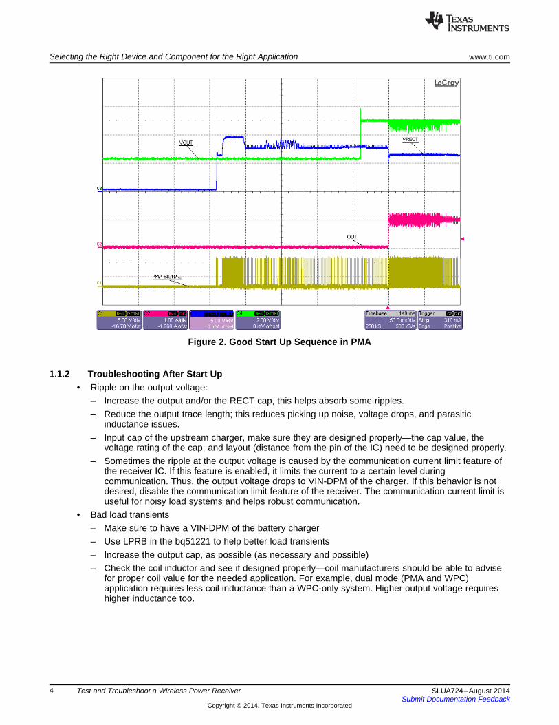
• Modulation depth– If a modulation depth does not meet the requirement for PMA and/or WPC, increase the
communication cap values. If the communication pocket in WPC-only system is too high, reducethe COMM caps. 22 nF to 100 nF is the recommended range.
– Check if the voltage rating on the caps is as recommended by the datasheet or the user’s guide ofthe part (mostly, at least 25 V is required).
– Make sure the COMM caps are placed as close to the IC as possible and not corrupted by noisytraces.
– A good PMA modulation depth plot is shown in Figure 3.
Figure 3. Modulation Depth in PMA System
• Triggering overvoltage protection (OVP) of the RX during start up or during load transients– The coil inductor is too high and causes the rectifier voltage to overshoot to 15 V during startup or
during load transients– Reduce the inductor for better transient response for this case– Reducing the coupling also helps
• OVP on the upstream charger is triggered– Increase the OVP level of the charger– If possible, reduce the VOUT level of the receiver– Increase the output caps of the receiver and/or the input cap of the charger
5SLUA724–August 2014 Test and Troubleshoot a Wireless Power ReceiverSubmit Documentation Feedback
Copyright © 2014, Texas Instruments Incorporated
Selecting the Right Device and Component for the Right Application www.ti.com
• Saturation and weak coil issues– To confirm that the coil is saturating, measure the transmitter operating frequency. If the frequency
is near the minimum of operating frequency range, then the RX coil is saturating or weak. Usually,under this condition the coil is not able to deliver full load power.
– To fix this, the shielding needs to be improved to increase the mutual inductance of the system– Increase the inductance of the coil– Change the shape and the size of the coil, including reducing the Z distance between the RX and
TX coils• Soldering issues
– We have seen this before, some customer issues are happening due to bad soldering of somecomponents in the board.
– Try to use different boards when debugging to avoid this issue– Use common sense and eye inspection, if possible, to avoid this situation; otherwise hours of
debugging will be spent for a simple bad connection of the component on the board.
6 Test and Troubleshoot a Wireless Power Receiver SLUA724–August 2014Submit Documentation Feedback
Copyright © 2014, Texas Instruments Incorporated
Output Current and OutVoltage Measurements
www.ti.com Efficiency Check
2 Efficiency CheckCompare the efficiency number with the datasheet and the data provided in the user guide. There are twotypes of efficiency commonly measured in wireless power systems:1. DC/DC efficiency checks for the whole system (from the DC input of the TX to the DC output of the
RX)2. AC/DC efficiency checks only the receiver side (AC input of the secondary coil to DC output of the RX)
• Efficiency = POUT / PIN = {I × V(DC)} / {I_AC × V_AC × cos(ϕ)}
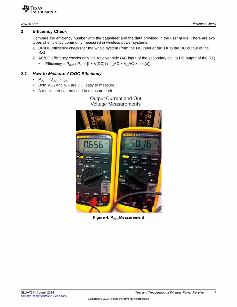
2.1 How to Measure AC/DC Efficiency• POUT = VOUT × IOUT
• Both VOUT and IOUT are DC, easy to measure• A multimeter can be used to measure both
Figure 4. POUT Measurement
7SLUA724–August 2014 Test and Troubleshoot a Wireless Power ReceiverSubmit Documentation Feedback
Copyright © 2014, Texas Instruments Incorporated
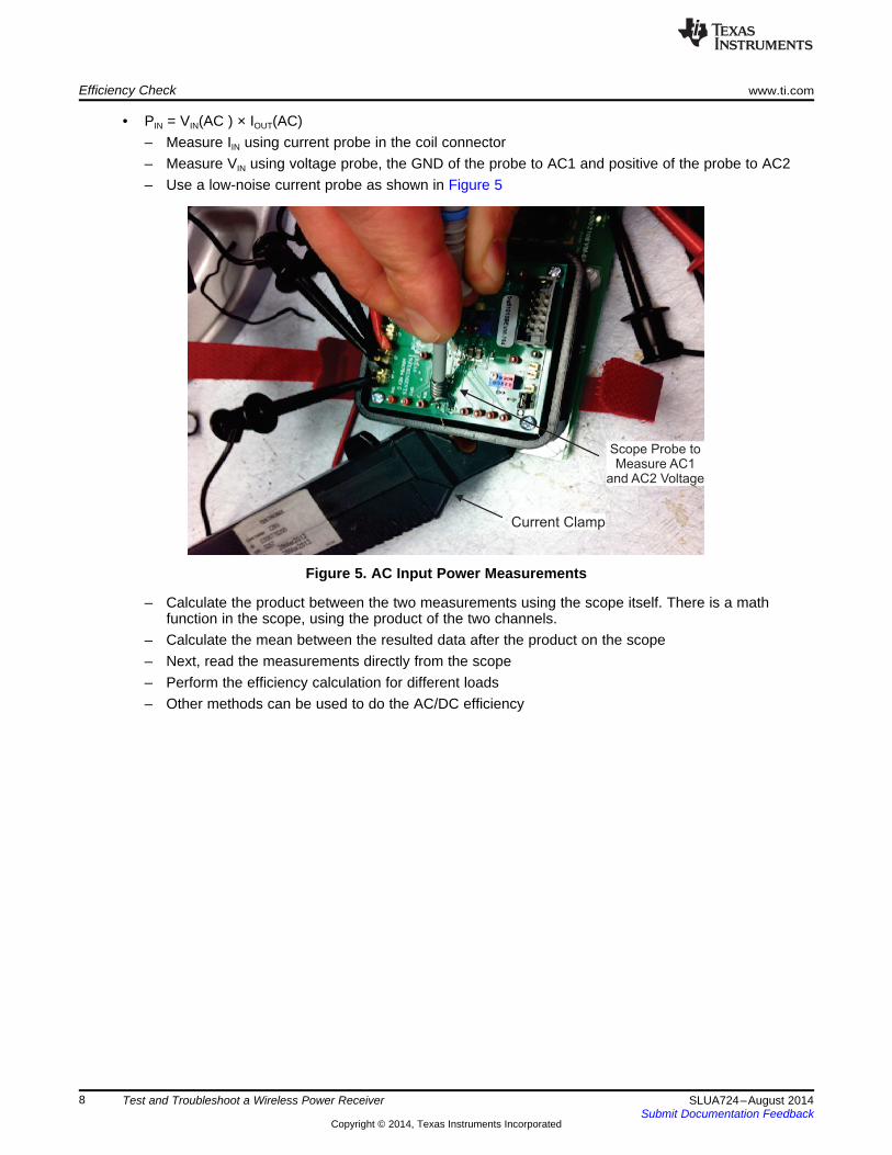
Current Clamp
Scope Probe toMeasure AC1
and AC2 Voltage
Efficiency Check www.ti.com
• PIN = VIN(AC ) × IOUT(AC)– Measure IIN using current probe in the coil connector– Measure VIN using voltage probe, the GND of the probe to AC1 and positive of the probe to AC2– Use a low-noise current probe as shown in Figure 5
Figure 5. AC Input Power Measurements
– Calculate the product between the two measurements using the scope itself. There is a mathfunction in the scope, using the product of the two channels.
– Calculate the mean between the resulted data after the product on the scope– Next, read the measurements directly from the scope– Perform the efficiency calculation for different loads– Other methods can be used to do the AC/DC efficiency
8 Test and Troubleshoot a Wireless Power Receiver SLUA724–August 2014Submit Documentation Feedback
Copyright © 2014, Texas Instruments Incorporated

www.ti.com Thermal Issues
3 Thermal IssuesOne of the main reasons for thermal issues on the board is bad layout. Make sure that power balls of theIC are connected to as much copper as possible in the WCSP package. Use power ground for powerdissipation to spread out the heat on a bigger copper surface.
Here are some other concerns when doing layout of a custom receiver PCB:• AC1 and AC2 trace resistance and width, losses on the trace will decrease thermal performance• OUT trace resistance• Good GND connection for thermal dissipation• COMM, CLAMP, BOOT capacitors connections• Use QFN package, if possible.• Copper weight (> 2 oz)• Number of layers, higher is better for thermal dissipation and flexibility
In addition to layout, a proper shielding of friendly objects is needed. Friendly objects are the metal objectsinside belonging to the end product. For example, in a smart phone there is battery frame, USB connector,camera, and so forth. These objects are made of metal and are located close enough to the coil, they canabsorb the magnetic flux. Any friendly metals closer to the flux field will absorb some of the transmittedenergy from the primary side. The energy is then transferred into heat and heats up the board over time.
4 Foreign Object Detection (FOD) CheckForeign objects are any metal objects outside and not belonging to the end product such as car keys,coins, and any other metals. These metals are close enough to the magnetic flux, they can absorb theenergy transmitted by the primary coil, therefore they heat up. As part of WPC1.1 requirements, foreignobject temperature is limited and must be controlled. One of the methods to limit temperature rise offoreign objects is to monitor and control the power losses from the transmitter to the receiver to foreignobjects during power transfer. This feature is called foreign object detection (FOD). If triggered, it maycause abnormal behavior.
The following steps can be used to troubleshoot:1. If a WPC 1.1 transmitter is used and the receiver is not tuned for FOD yet. Disable FOD on TX before
testing.2. The following symptoms indicate FOD: VOUT should be fluctuating and starts providing nearly 5 W, then
drops to no output and will retry.3. FOD calibration should be performed on the final configuration.4. If FOD calibration is performed on RX, any changes on the RX board will affect the calibration and has
to be done again.
9SLUA724–August 2014 Test and Troubleshoot a Wireless Power ReceiverSubmit Documentation Feedback
Copyright © 2014, Texas Instruments Incorporated

IMPORTANT NOTICE
Texas Instruments Incorporated and its subsidiaries (TI) reserve the right to make corrections, enhancements, improvements and otherchanges to its semiconductor products and services per JESD46, latest issue, and to discontinue any product or service per JESD48, latestissue. Buyers should obtain the latest relevant information before placing orders and should verify that such information is current andcomplete. All semiconductor products (also referred to herein as “components”) are sold subject to TI’s terms and conditions of salesupplied at the time of order acknowledgment.TI warrants performance of its components to the specifications applicable at the time of sale, in accordance with the warranty in TI’s termsand conditions of sale of semiconductor products. Testing and other quality control techniques are used to the extent TI deems necessaryto support this warranty. Except where mandated by applicable law, testing of all parameters of each component is not necessarilyperformed.TI assumes no liability for applications assistance or the design of Buyers’ products. Buyers are responsible for their products andapplications using TI components. To minimize the risks associated with Buyers’ products and applications, Buyers should provideadequate design and operating safeguards.TI does not warrant or represent that any license, either express or implied, is granted under any patent right, copyright, mask work right, orother intellectual property right relating to any combination, machine, or process in which TI components or services are used. Informationpublished by TI regarding third-party products or services does not constitute a license to use such products or services or a warranty orendorsement thereof. Use of such information may require a license from a third party under the patents or other intellectual property of thethird party, or a license from TI under the patents or other intellectual property of TI.Reproduction of significant portions of TI information in TI data books or data sheets is permissible only if reproduction is without alterationand is accompanied by all associated warranties, conditions, limitations, and notices. TI is not responsible or liable for such altereddocumentation. Information of third parties may be subject to additional restrictions.Resale of TI components or services with statements different from or beyond the parameters stated by TI for that component or servicevoids all express and any implied warranties for the associated TI component or service and is an unfair and deceptive business practice.TI is not responsible or liable for any such statements.Buyer acknowledges and agrees that it is solely responsible for compliance with all legal, regulatory and safety-related requirementsconcerning its products, and any use of TI components in its applications, notwithstanding any applications-related information or supportthat may be provided by TI. Buyer represents and agrees that it has all the necessary expertise to create and implement safeguards whichanticipate dangerous consequences of failures, monitor failures and their consequences, lessen the likelihood of failures that might causeharm and take appropriate remedial actions. Buyer will fully indemnify TI and its representatives against any damages arising out of the useof any TI components in safety-critical applications.In some cases, TI components may be promoted specifically to facilitate safety-related applications. With such components, TI’s goal is tohelp enable customers to design and create their own end-product solutions that meet applicable functional safety standards andrequirements. Nonetheless, such components are subject to these terms.No TI components are authorized for use in FDA Class III (or similar life-critical medical equipment) unless authorized officers of the partieshave executed a special agreement specifically governing such use.Only those TI components which TI has specifically designated as military grade or “enhanced plastic” are designed and intended for use inmilitary/aerospace applications or environments. Buyer acknowledges and agrees that any military or aerospace use of TI componentswhich have not been so designated is solely at the Buyer's risk, and that Buyer is solely responsible for compliance with all legal andregulatory requirements in connection with such use.TI has specifically designated certain components as meeting ISO/TS16949 requirements, mainly for automotive use. In any case of use ofnon-designated products, TI will not be responsible for any failure to meet ISO/TS16949.
Products ApplicationsAudio www.ti.com/audio Automotive and Transportation www.ti.com/automotiveAmplifiers amplifier.ti.com Communications and Telecom www.ti.com/communicationsData Converters dataconverter.ti.com Computers and Peripherals www.ti.com/computersDLP® Products www.dlp.com Consumer Electronics www.ti.com/consumer-appsDSP dsp.ti.com Energy and Lighting www.ti.com/energyClocks and Timers www.ti.com/clocks Industrial www.ti.com/industrialInterface interface.ti.com Medical www.ti.com/medicalLogic logic.ti.com Security www.ti.com/securityPower Mgmt power.ti.com Space, Avionics and Defense www.ti.com/space-avionics-defenseMicrocontrollers microcontroller.ti.com Video and Imaging www.ti.com/videoRFID www.ti-rfid.comOMAP Applications Processors www.ti.com/omap TI E2E Community e2e.ti.comWireless Connectivity www.ti.com/wirelessconnectivity
Mailing Address: Texas Instruments, Post Office Box 655303, Dallas, Texas 75265Copyright © 2014, Texas Instruments Incorporated