Embed Size (px)
Citation preview
MAHARASHTRA STATE BOARD OF TECHNICAL EDUCATION (Autonomous)
(ISO/IEC - 27001 - 2013 Certified)
____________________________________________________________________________________________
Page 1 of 38
WINTER– 17 EXAMINATION Subject Name: Linear Integrated Circuits Model Answer Subject Code:
I m p o r t a n t I n s t r u c t i o n s t o e x a m i n e r s : 1) The answers should be examined by key words and not as word-to-word as given
in the model answer scheme. 2) The model answer and the answer written by candidate may vary but the examiner
may try to assess the understanding level of the candidate. 3) The language errors such as grammatical, spelling errors should not be given more
Importance (Not applicable for subject English and Communication Skills. 4) While assessing figures, examiner may give credit for principal components
indicated in the figure. The figures drawn by candidate and model answer may vary. The examiner may give credit for any equivalent figure drawn.
5) Credits may be given step wise for numerical problems. In some cases, the assumed constant values may vary and there may be some difference in the candidate’s answers and model answer.
6) In case of some questions credit may be given by judgement on part of examiner of relevant answer based on candidate’s understanding.
7) For programming language papers, credit may be given to any other program based on equivalent concept.
17445
MAHARASHTRA STATE BOARD OF TECHNICAL EDUCATION (Autonomous)
(ISO/IEC - 27001 - 2013 Certified)
____________________________________________________________________________________________
Page 2 of 38
Q.1 a) Attempt any SIX of the following : 12 marks
(i) State ideal and typical values of
1) Slew rate
2) CMRR
Ans :-(Each value – ½ mks)
Typical values of Ideal values
1) Slew rate = 0.5 V/µs Infinite
2) CMMR = 90 dB Infinite
(ii) State the need of signal conditioning (two points)
Ans :-( Need – 2 mks)
Need of signal conditioning
(iii) List specifications of IC LM 324 .
Ans :- (Any four -2 Mks)
Specifications of IC LM 324
1) Short Circuited Protected Outputs
2) True Differential Input Stage
3) Single Supply Operation: 3.0 V to 32 V
4) Low Input Bias Currents: 100 nA Maximum
5) Four Amplifiers Per Package
6) Internally Compensated
7) Common Mode Range Extends to Negative Supply
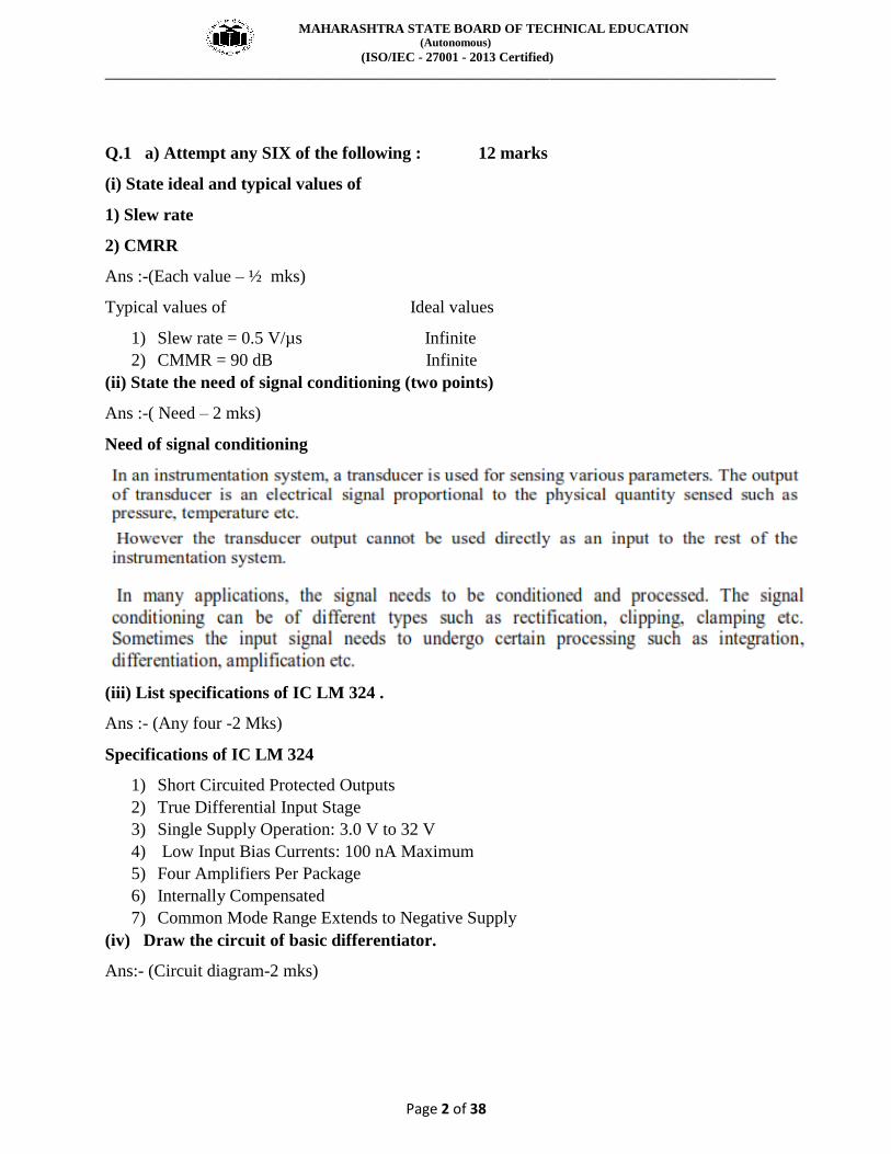
(iv) Draw the circuit of basic differentiator.
Ans:- (Circuit diagram-2 mks)
MAHARASHTRA STATE BOARD OF TECHNICAL EDUCATION (Autonomous)
(ISO/IEC - 27001 - 2013 Certified)
____________________________________________________________________________________________
Page 3 of 38
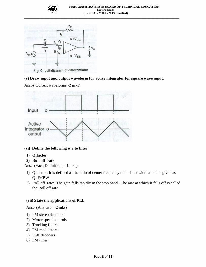
(v) Draw input and output waveform for active integrator for square wave input.
Ans:-( Correct waveforms -2 mks)
(vi) Define the following w.r.to filter
1) Q factor
2) Roll off rate
Ans:- (Each Definition – 1 mks)
1) Q factor : It is defined as the ratio of center frequency to the bandwidth and it is given as
Q=Fc/BW
2) Roll off rate: The gain falls rapidly in the stop band . The rate at which it falls off is called
the Roll off rate.
(vii) State the applications of PLL
Ans:- (Any two – 2 mks)
1) FM stereo decoders
2) Motor speed controls
3) Tracking filters
4) FM modulators
5) FSK decoders
6) FM tuner

MAHARASHTRA STATE BOARD OF TECHNICAL EDUCATION (Autonomous)
(ISO/IEC - 27001 - 2013 Certified)
____________________________________________________________________________________________
Page 4 of 38
7) Generation of local oscillator frequency
(viii) Define :
1) Output voltage swing
2) SVRR
Ans:- ( Each Definition -1mks)
1) Output voltage swing : The output voltage swing indicates the value of positive and
negative saturation voltages of op-amp.
2) SVRR: The change in op-amp’s input offset voltage Vio, cause by variation in supply
voltage is called supply voltage rejection ratio (SVRR).
b) Attempt any TWO of the following: 8
( i) Draw block diagram of OPAMP and state the function of constant current source and
Output stage.
Ans:- ( Block diagram- 2 mks,, functions- 1 mks each)
Constant current source stage:
Constant current source provides low output resistance and high CMRR.
Output Stage: This stage uses complementary symmetry push pull amplifier. This stage
provides low output resistance and hence increases the current supplying capability of op-amp
and also this stage increases the output voltage swing.
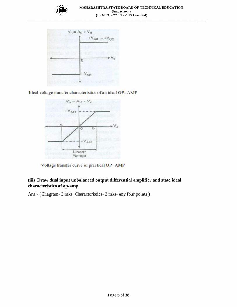
ii) Draw ideal and practical voltage transfer characteristics of OP-AMP.
Ans:- ( Each characteristics- 2 mks )
MAHARASHTRA STATE BOARD OF TECHNICAL EDUCATION (Autonomous)
(ISO/IEC - 27001 - 2013 Certified)
____________________________________________________________________________________________
Page 5 of 38
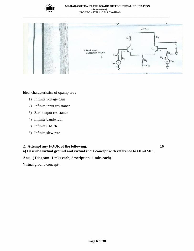
(iii) Draw dual input unbalanced output differential amplifier and state ideal
characteristics of op-amp
Ans:- ( Diagram- 2 mks, Characteristics- 2 mks- any four points )
MAHARASHTRA STATE BOARD OF TECHNICAL EDUCATION (Autonomous)
(ISO/IEC - 27001 - 2013 Certified)
____________________________________________________________________________________________
Page 6 of 38
Ideal characteristics of opamp are :
1) Infinite voltage gain
2) Infinite input resistance
3) Zero output resistance
4) Infinite bandwidth
5) Infinite CMRR
6) Infinite slew rate
2. Attempt any FOUR of the following: 16
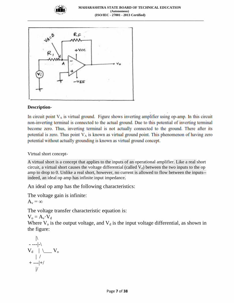
a) Describe virtual ground and virtual short concept with reference to OP-AMP.
Ans:- ( Diagram- 1 mks each, description- 1 mks each)
Virtual ground concept-
MAHARASHTRA STATE BOARD OF TECHNICAL EDUCATION (Autonomous)
(ISO/IEC - 27001 - 2013 Certified)
____________________________________________________________________________________________
Page 7 of 38
Description-
Virtual short concept-
A virtual short is a concept that applies to the inputs of an operational amplifier. Like a real short
circuit, a virtual short causes the voltage differential (called Vd) between the two inputs to the op
amp to drop to 0. Unlike a real short, however, no current is allowed to flow between the inputs--
indeed, an ideal op amp has infinite input impedance.
An ideal op amp has the following characteristics:
The voltage gain is infinite:
Av = ∞
The voltage transfer characteristic equation is:
Vo = Av·Vd
Where Vo is the output voltage, and Vd is the input voltage differential, as shown in
the figure:
|\
- ---|-\
Vd | \___ Vo
| /
+ ---|+/
|/
MAHARASHTRA STATE BOARD OF TECHNICAL EDUCATION (Autonomous)
(ISO/IEC - 27001 - 2013 Certified)
____________________________________________________________________________________________
Page 8 of 38
Then, if we express Vd in terms of Vo, we get:
Vd = Vo / Av
And, substituting in Av:
Vd = Vo / ∞ = 0
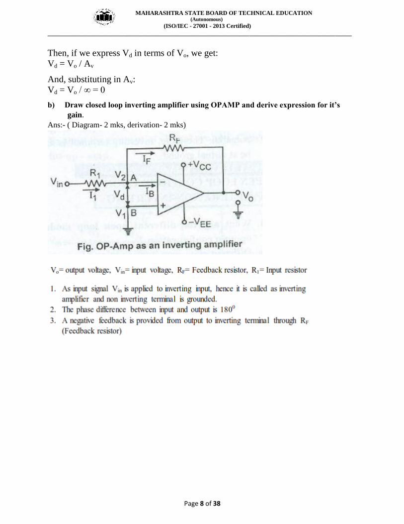
b) Draw closed loop inverting amplifier using OPAMP and derive expression for it’s
gain.
Ans:- ( Diagram- 2 mks, derivation- 2 mks)
MAHARASHTRA STATE BOARD OF TECHNICAL EDUCATION (Autonomous)
(ISO/IEC - 27001 - 2013 Certified)
____________________________________________________________________________________________
Page 9 of 38
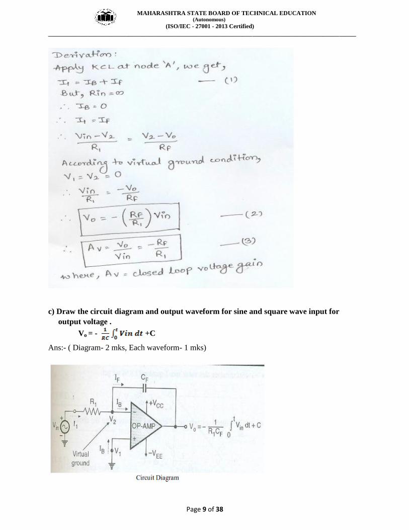
c) Draw the circuit diagram and output waveform for sine and square wave input for
output voltage .
Vo = - +C
Ans:- ( Diagram- 2 mks, Each waveform- 1 mks)
MAHARASHTRA STATE BOARD OF TECHNICAL EDUCATION (Autonomous)
(ISO/IEC - 27001 - 2013 Certified)
____________________________________________________________________________________________
Page 10 of 38
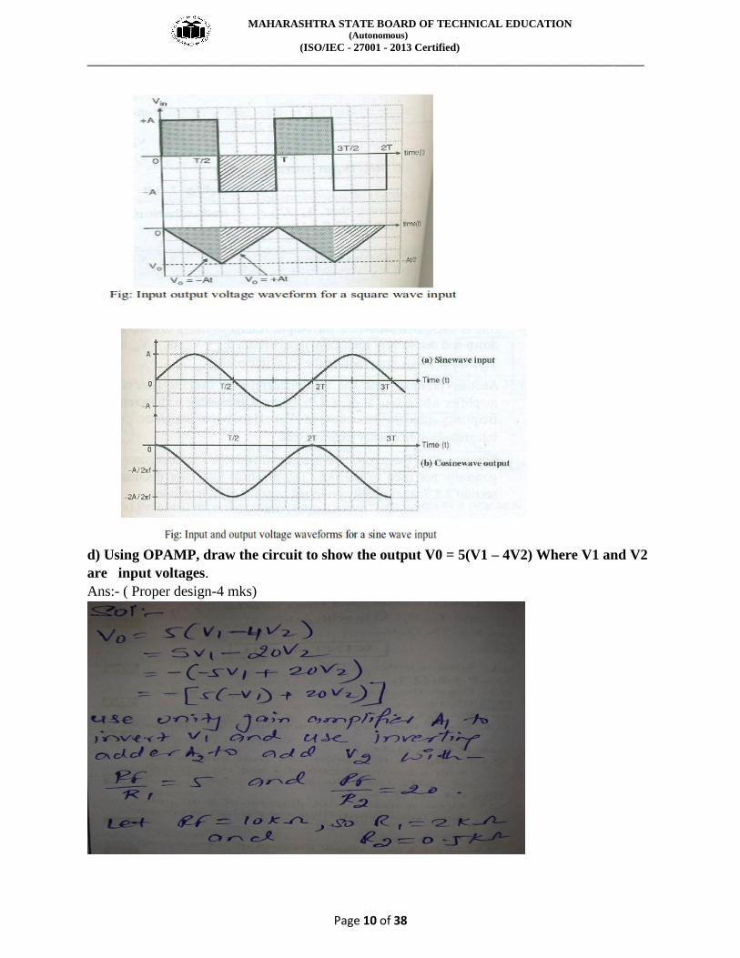
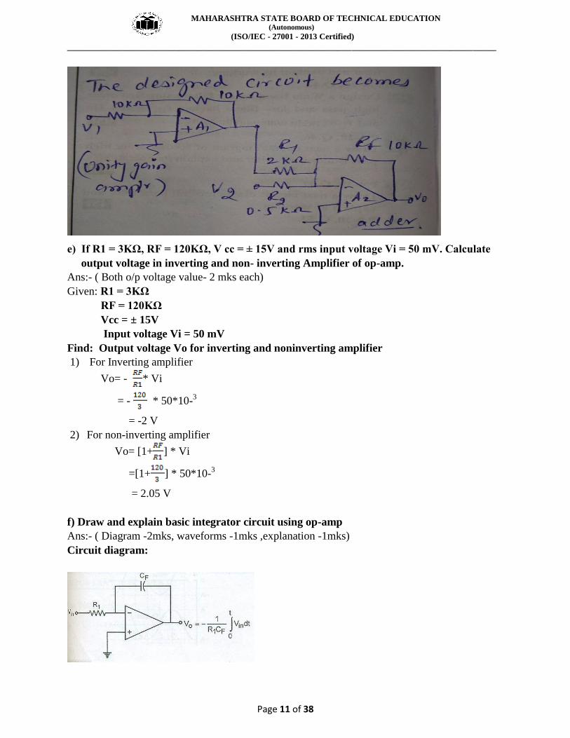
d) Using OPAMP, draw the circuit to show the output V0 = 5(V1 – 4V2) Where V1 and V2
are input voltages.
Ans:- ( Proper design-4 mks)
MAHARASHTRA STATE BOARD OF TECHNICAL EDUCATION (Autonomous)
(ISO/IEC - 27001 - 2013 Certified)
____________________________________________________________________________________________
Page 11 of 38
e) If R1 = 3KΩ, RF = 120KΩ, V cc = ± 15V and rms input voltage Vi = 50 mV. Calculate
output voltage in inverting and non- inverting Amplifier of op-amp.
Ans:- ( Both o/p voltage value- 2 mks each)
Given: R1 = 3KΩ
RF = 120KΩ
Vcc = ± 15V
Input voltage Vi = 50 mV
Find: Output voltage Vo for inverting and noninverting amplifier
1) For Inverting amplifier
Vo= - * Vi
= - * 50*10-3
= -2 V
2) For non-inverting amplifier
Vo= [1+ ] * Vi
=[1+ ] * 50*10-3
= 2.05 V
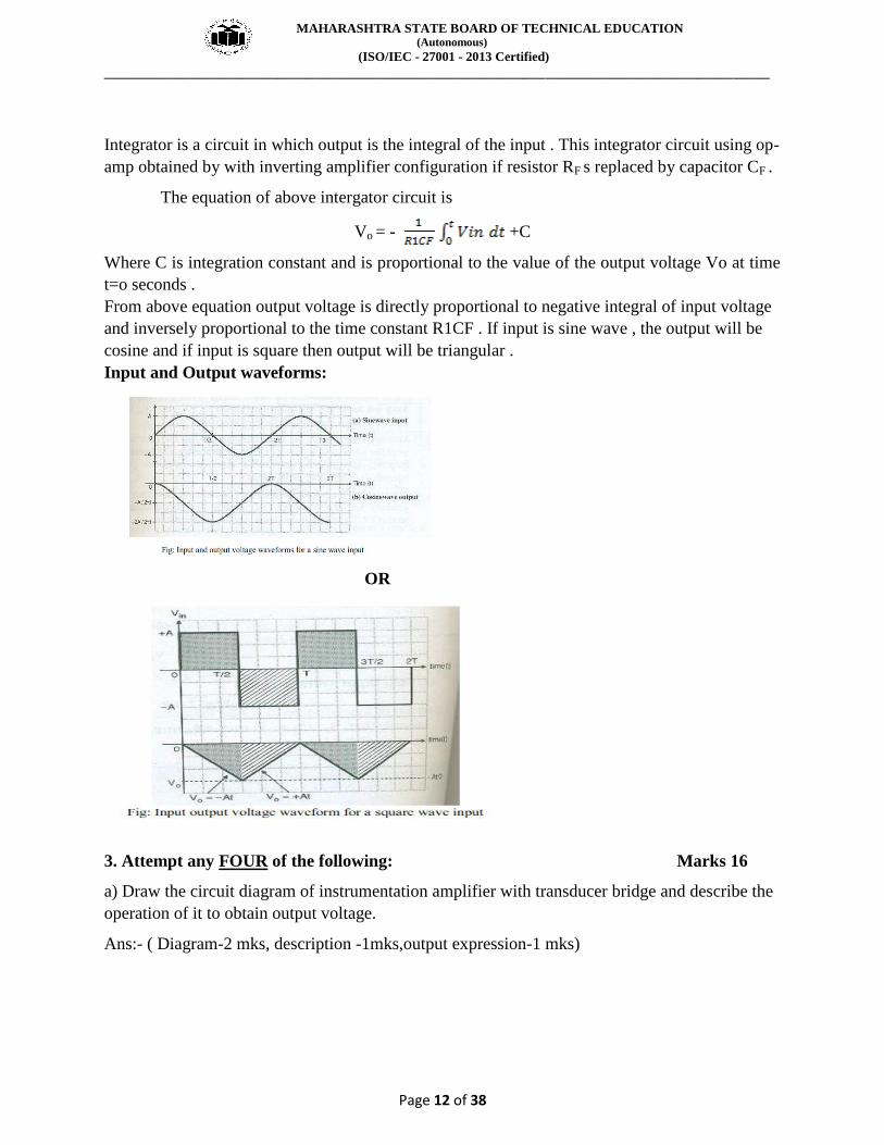
f) Draw and explain basic integrator circuit using op-amp
Ans:- ( Diagram -2mks, waveforms -1mks ,explanation -1mks)
Circuit diagram:
MAHARASHTRA STATE BOARD OF TECHNICAL EDUCATION (Autonomous)
(ISO/IEC - 27001 - 2013 Certified)
____________________________________________________________________________________________
Page 12 of 38
Integrator is a circuit in which output is the integral of the input . This integrator circuit using op-
amp obtained by with inverting amplifier configuration if resistor RF s replaced by capacitor CF .
The equation of above intergator circuit is
Vo = - +C
Where C is integration constant and is proportional to the value of the output voltage Vo at time
t=o seconds .
From above equation output voltage is directly proportional to negative integral of input voltage
and inversely proportional to the time constant R1CF . If input is sine wave , the output will be
cosine and if input is square then output will be triangular .
Input and Output waveforms:
OR
3. Attempt any FOUR of the following: Marks 16
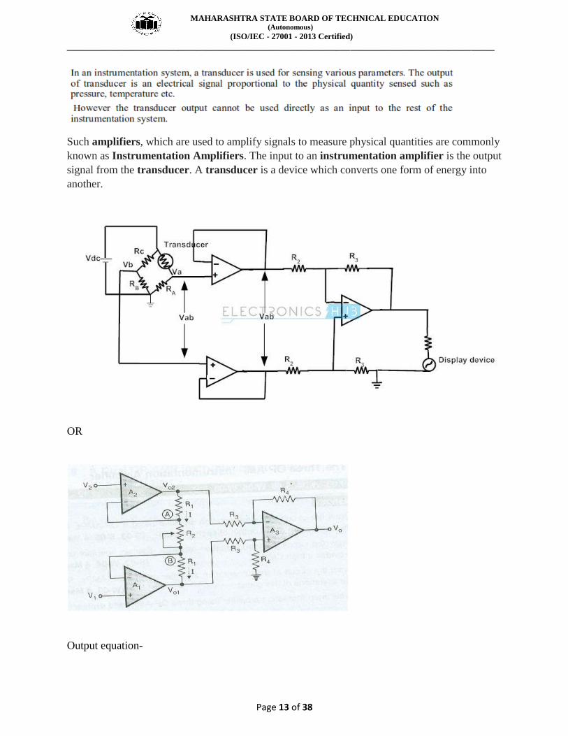
a) Draw the circuit diagram of instrumentation amplifier with transducer bridge and describe the
operation of it to obtain output voltage.
Ans:- ( Diagram-2 mks, description -1mks,output expression-1 mks)
MAHARASHTRA STATE BOARD OF TECHNICAL EDUCATION (Autonomous)
(ISO/IEC - 27001 - 2013 Certified)
____________________________________________________________________________________________
Page 13 of 38
Such amplifiers, which are used to amplify signals to measure physical quantities are commonly
known as Instrumentation Amplifiers. The input to an instrumentation amplifier is the output
signal from the transducer. A transducer is a device which converts one form of energy into
another.
OR
Output equation-
MAHARASHTRA STATE BOARD OF TECHNICAL EDUCATION (Autonomous)
(ISO/IEC - 27001 - 2013 Certified)
____________________________________________________________________________________________
Page 14 of 38
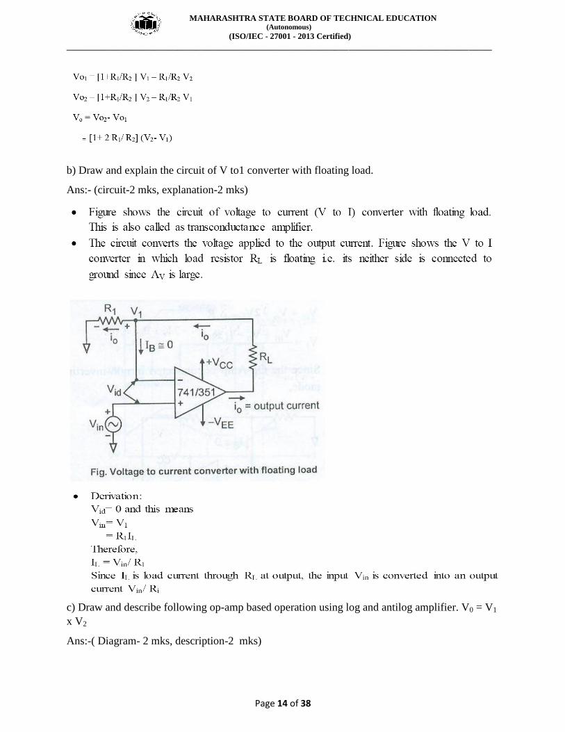
b) Draw and explain the circuit of V to1 converter with floating load.
Ans:- (circuit-2 mks, explanation-2 mks)
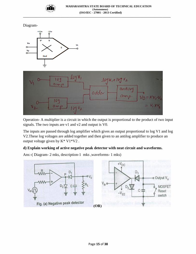
c) Draw and describe following op-amp based operation using log and antilog amplifier. V0 = V1
x V2
Ans:-( Diagram- 2 mks, description-2 mks)
MAHARASHTRA STATE BOARD OF TECHNICAL EDUCATION (Autonomous)
(ISO/IEC - 27001 - 2013 Certified)
____________________________________________________________________________________________
Page 15 of 38
Diagram-
Operation- A multiplier is a circuit in which the output is proportional to the product of two input
signals. The two inputs are v1 and v2 and output is V0.
The inputs are passed through log amplifier which gives an output proportional to log V1 and log
V2.These log voltages are added together and then given to an antilog amplifier to produce an
output voltage given by K* V1*V2 .
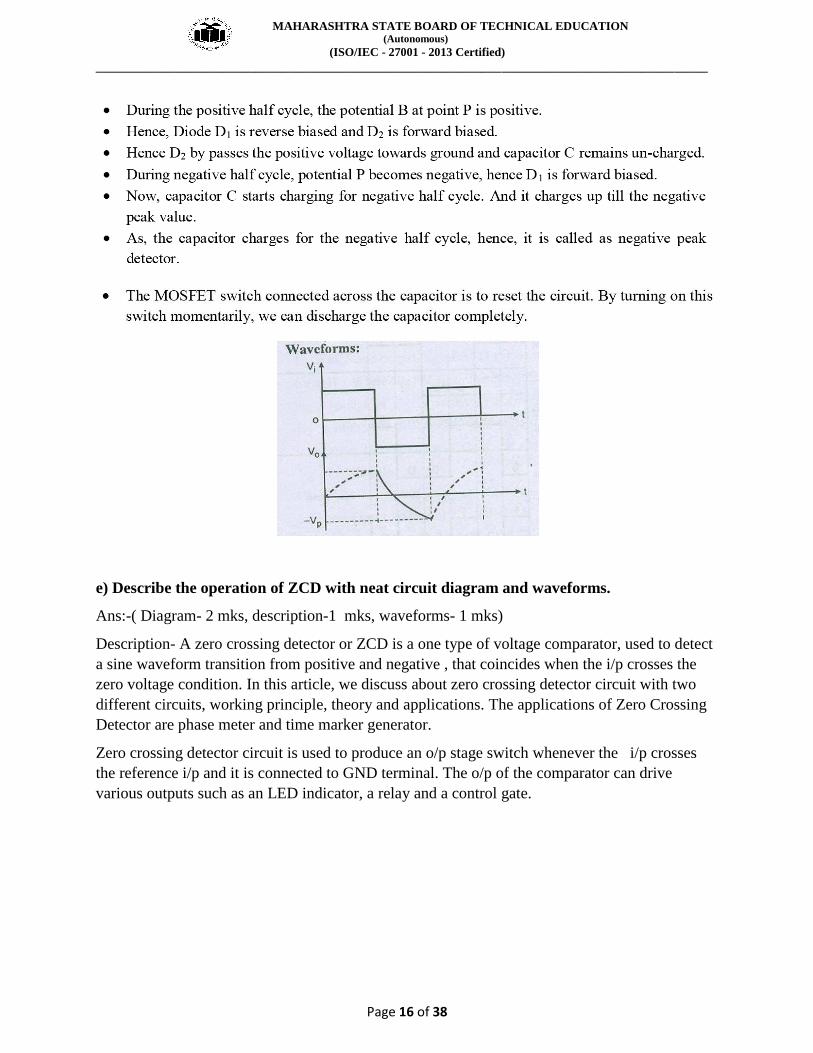
d) Explain working of active negative peak detector with neat circuit and waveforms.
Ans:-( Diagram- 2 mks, description-1 mks ,waveforms- 1 mks)
MAHARASHTRA STATE BOARD OF TECHNICAL EDUCATION (Autonomous)
(ISO/IEC - 27001 - 2013 Certified)
____________________________________________________________________________________________
Page 16 of 38
e) Describe the operation of ZCD with neat circuit diagram and waveforms.
Ans:-( Diagram- 2 mks, description-1 mks, waveforms- 1 mks)
Description- A zero crossing detector or ZCD is a one type of voltage comparator, used to detect
a sine waveform transition from positive and negative , that coincides when the i/p crosses the
zero voltage condition. In this article, we discuss about zero crossing detector circuit with two
different circuits, working principle, theory and applications. The applications of Zero Crossing
Detector are phase meter and time marker generator.
Zero crossing detector circuit is used to produce an o/p stage switch whenever the i/p crosses
the reference i/p and it is connected to GND terminal. The o/p of the comparator can drive
various outputs such as an LED indicator, a relay and a control gate.
MAHARASHTRA STATE BOARD OF TECHNICAL EDUCATION (Autonomous)
(ISO/IEC - 27001 - 2013 Certified)
____________________________________________________________________________________________
Page 17 of 38
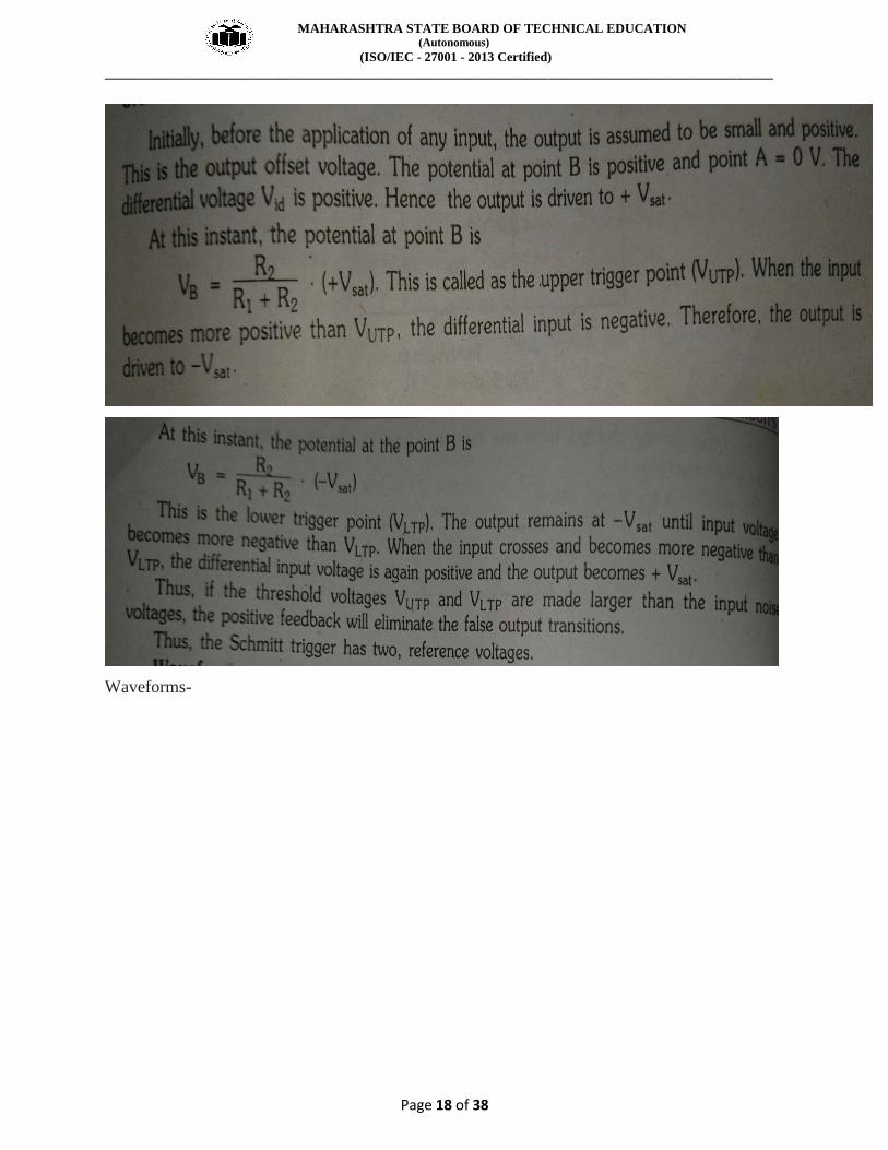
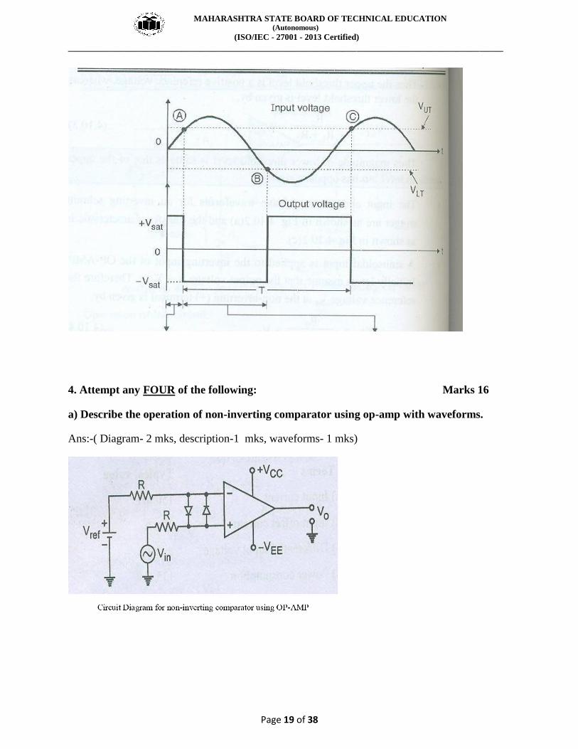
f) Draw circuit diagram and input output waveforms of op-amp based Schmitt trigger.
Ans:-( Diagram- 2 mks, description-2 mks)
Description-
MAHARASHTRA STATE BOARD OF TECHNICAL EDUCATION (Autonomous)
(ISO/IEC - 27001 - 2013 Certified)
____________________________________________________________________________________________
Page 18 of 38
Waveforms-
MAHARASHTRA STATE BOARD OF TECHNICAL EDUCATION (Autonomous)
(ISO/IEC - 27001 - 2013 Certified)
____________________________________________________________________________________________
Page 19 of 38
4. Attempt any FOUR of the following: Marks 16
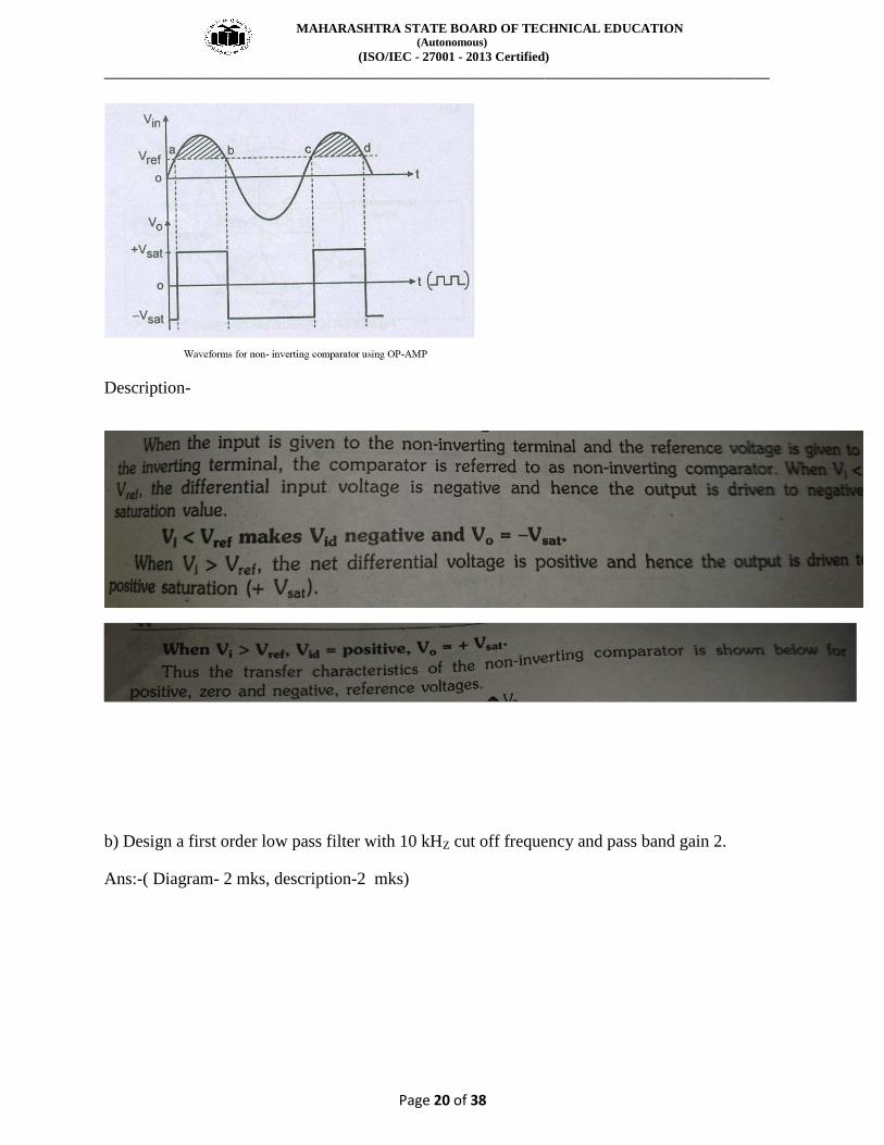
a) Describe the operation of non-inverting comparator using op-amp with waveforms.
Ans:-( Diagram- 2 mks, description-1 mks, waveforms- 1 mks)
MAHARASHTRA STATE BOARD OF TECHNICAL EDUCATION (Autonomous)
(ISO/IEC - 27001 - 2013 Certified)
____________________________________________________________________________________________
Page 20 of 38
Description-
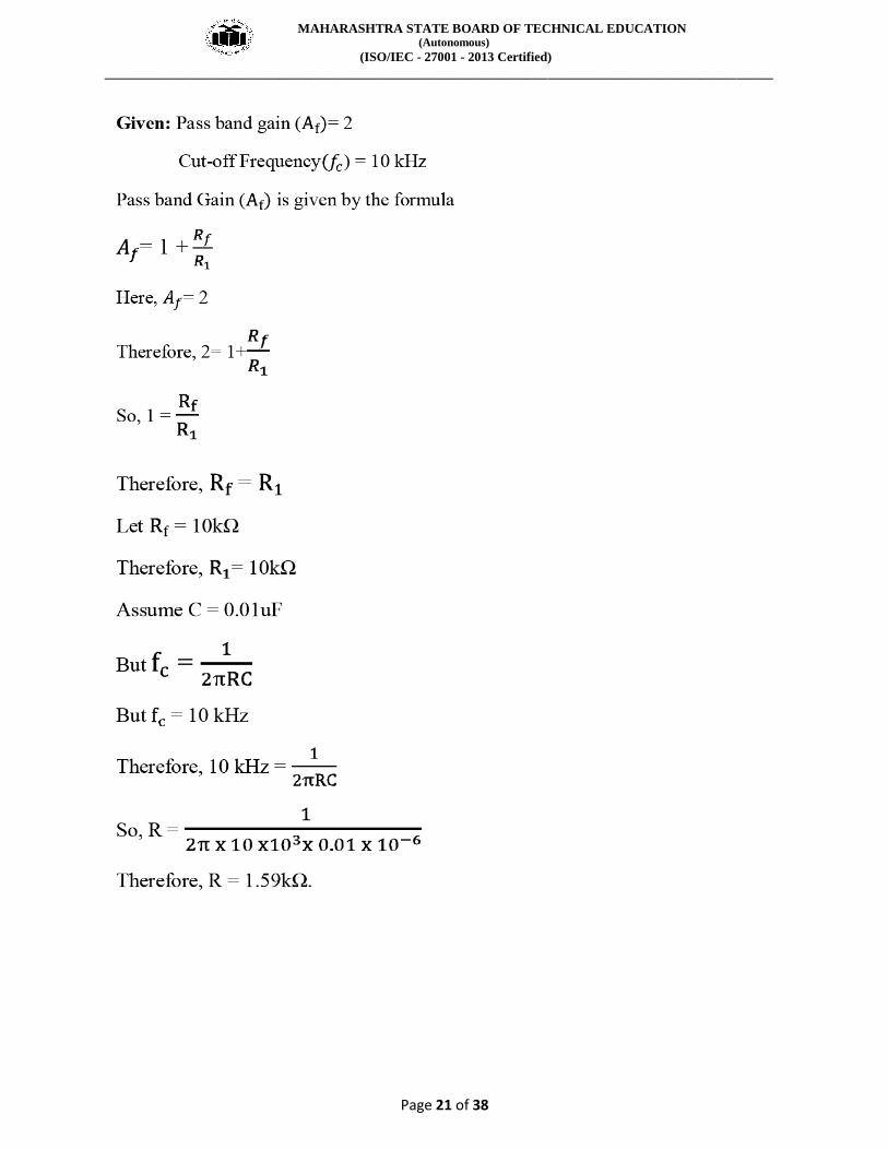
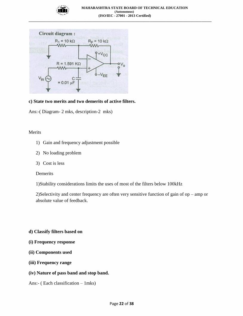
b) Design a first order low pass filter with 10 kHZ cut off frequency and pass band gain 2.
Ans:-( Diagram- 2 mks, description-2 mks)
MAHARASHTRA STATE BOARD OF TECHNICAL EDUCATION (Autonomous)
(ISO/IEC - 27001 - 2013 Certified)
____________________________________________________________________________________________
Page 21 of 38
MAHARASHTRA STATE BOARD OF TECHNICAL EDUCATION (Autonomous)
(ISO/IEC - 27001 - 2013 Certified)
____________________________________________________________________________________________
Page 22 of 38
c) State two merits and two demerits of active filters.
Ans:-( Diagram- 2 mks, description-2 mks)
Merits
1) Gain and frequency adjustment possible
2) No loading problem
3) Cost is less
Demerits
1)Stability considerations limits the uses of most of the filters below 100kHz
2)Selectivity and center frequency are often very sensitive function of gain of op – amp or
absolute value of feedback.
d) Classify filters based on
(i) Frequency response
(ii) Components used
(iii) Frequency range
(iv) Nature of pass band and stop band.
Ans:- ( Each classification – 1mks)
MAHARASHTRA STATE BOARD OF TECHNICAL EDUCATION (Autonomous)
(ISO/IEC - 27001 - 2013 Certified)
____________________________________________________________________________________________
Page 23 of 38
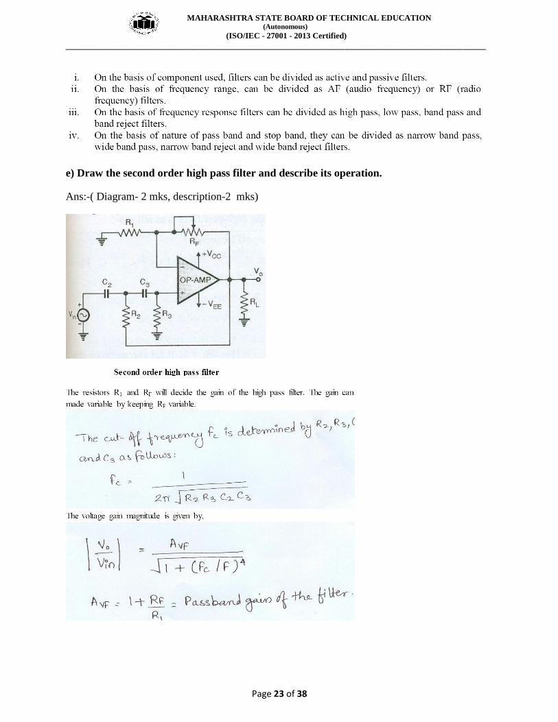
e) Draw the second order high pass filter and describe its operation.
Ans:-( Diagram- 2 mks, description-2 mks)
MAHARASHTRA STATE BOARD OF TECHNICAL EDUCATION (Autonomous)
(ISO/IEC - 27001 - 2013 Certified)
____________________________________________________________________________________________
Page 24 of 38
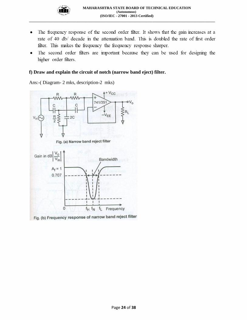
f) Draw and explain the circuit of notch (narrow band eject) filter.
Ans:-( Diagram- 2 mks, description-2 mks)
MAHARASHTRA STATE BOARD OF TECHNICAL EDUCATION (Autonomous)
(ISO/IEC - 27001 - 2013 Certified)
____________________________________________________________________________________________
Page 25 of 38
5. Attempt any FOUR of the following: Marks 16
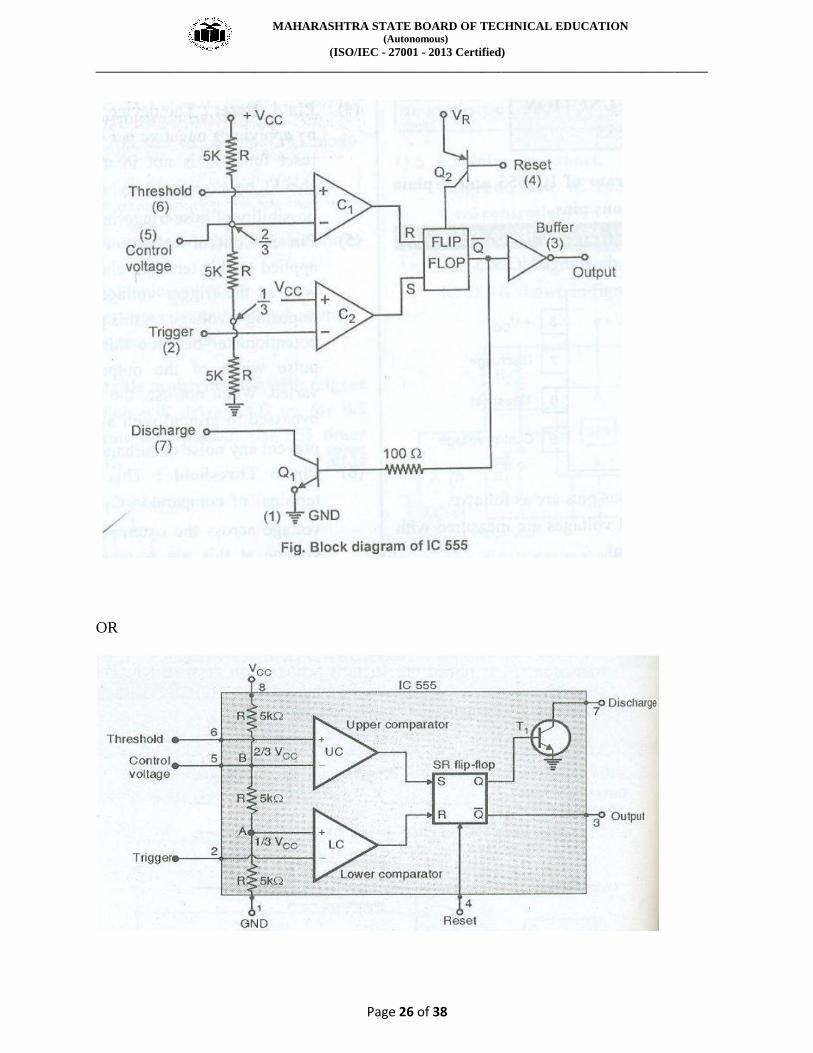
a) Draw the functional block diagram of Timer IC 555 and explain each block.
Ans:-( Diagram- 2 mks, description-2 mks)
MAHARASHTRA STATE BOARD OF TECHNICAL EDUCATION (Autonomous)
(ISO/IEC - 27001 - 2013 Certified)
____________________________________________________________________________________________
Page 26 of 38
OR
MAHARASHTRA STATE BOARD OF TECHNICAL EDUCATION (Autonomous)
(ISO/IEC - 27001 - 2013 Certified)
____________________________________________________________________________________________
Page 27 of 38
Explanation -
Comparator: The Comparator are the basic electronic component which compares the two input
voltages i.e. between the inverting (-) and the non-inverting (+) input and if the non-inverting
input is more than the inverting input then the output of the comparator is high. Also the input
resistance of an ideal comparator is infinite.
· Voltage Divider: As we know that the input resistance of the comparators is infinite hence
the input voltage is divided equally between the three resistors. The value being Vin/3 across
each resistor.
· Flip/Flop: Flip/Flop is a memory element of Digital-electronics. The output (Q) of the
flip/flop is ‘high’ if the input at ‘S’ terminal is ‘high’ and ‘R’ is at ‘Low’ and the output (Q) is
‘low’ when the input at ‘S’ is ‘low’ and at ‘R’ is high.
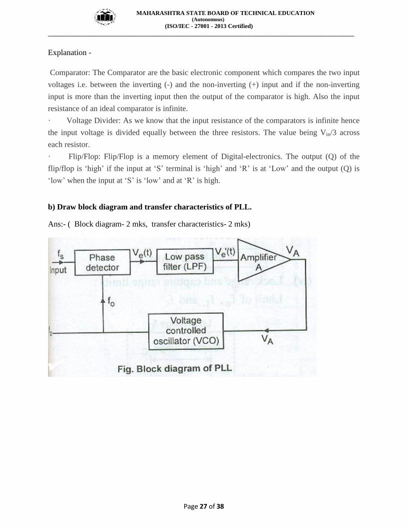
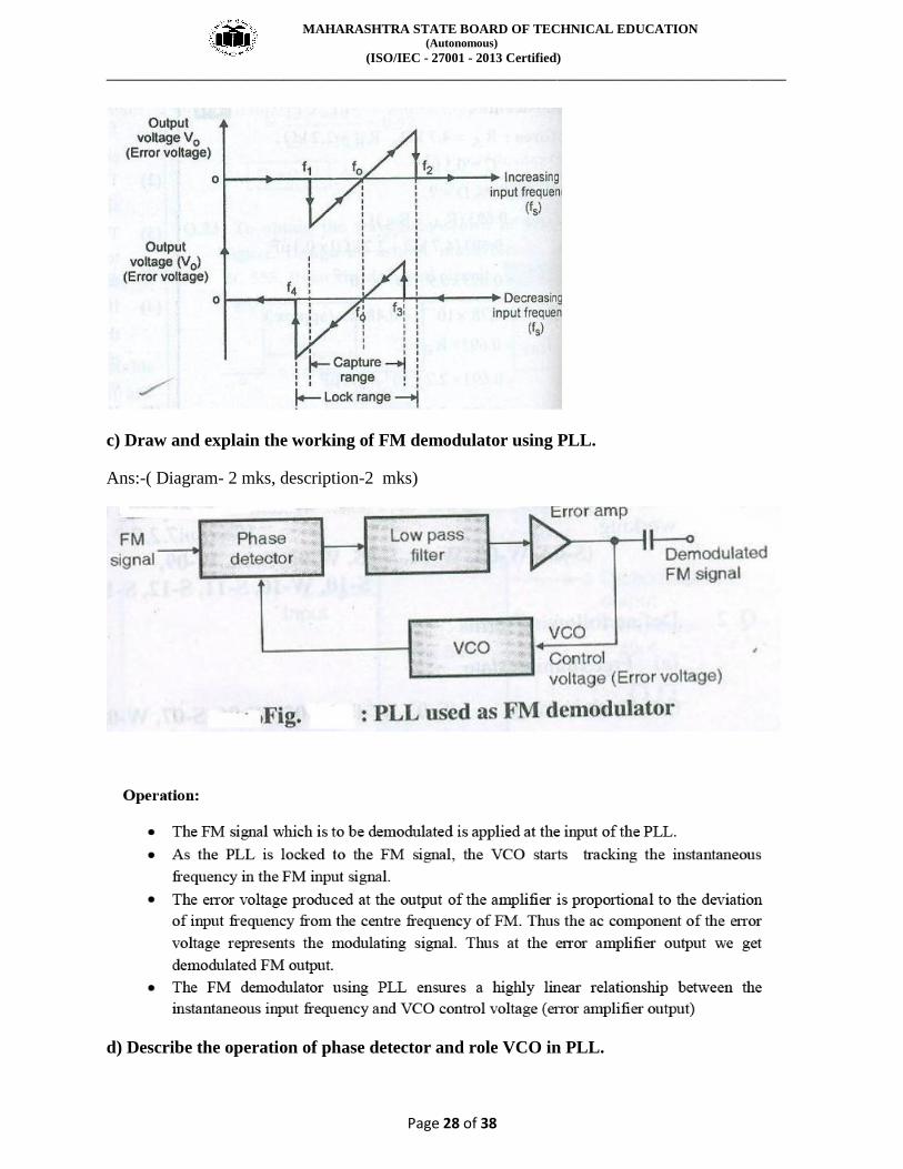
b) Draw block diagram and transfer characteristics of PLL.
Ans:- ( Block diagram- 2 mks, transfer characteristics- 2 mks)
MAHARASHTRA STATE BOARD OF TECHNICAL EDUCATION (Autonomous)
(ISO/IEC - 27001 - 2013 Certified)
____________________________________________________________________________________________
Page 28 of 38
c) Draw and explain the working of FM demodulator using PLL.
Ans:-( Diagram- 2 mks, description-2 mks)
d) Describe the operation of phase detector and role VCO in PLL.
MAHARASHTRA STATE BOARD OF TECHNICAL EDUCATION (Autonomous)
(ISO/IEC - 27001 - 2013 Certified)
____________________________________________________________________________________________
Page 29 of 38
Ans:-( Each description-2 mks)
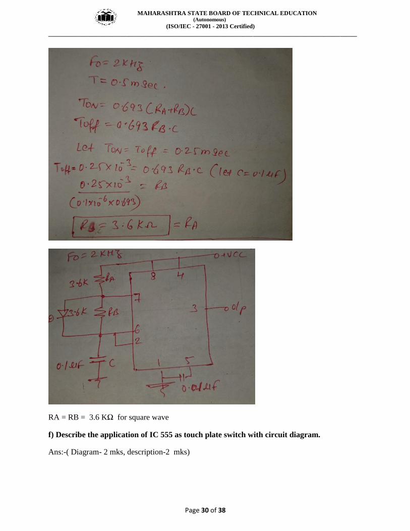
e) Design an Astable multivibrator using IC 555 timer for a frequency of 2 kHZ.
Ans:-( Diagram- 2 mks, description-2 mks)
MAHARASHTRA STATE BOARD OF TECHNICAL EDUCATION (Autonomous)
(ISO/IEC - 27001 - 2013 Certified)
____________________________________________________________________________________________
Page 30 of 38
RA = RB = 3.6 KΩ for square wave
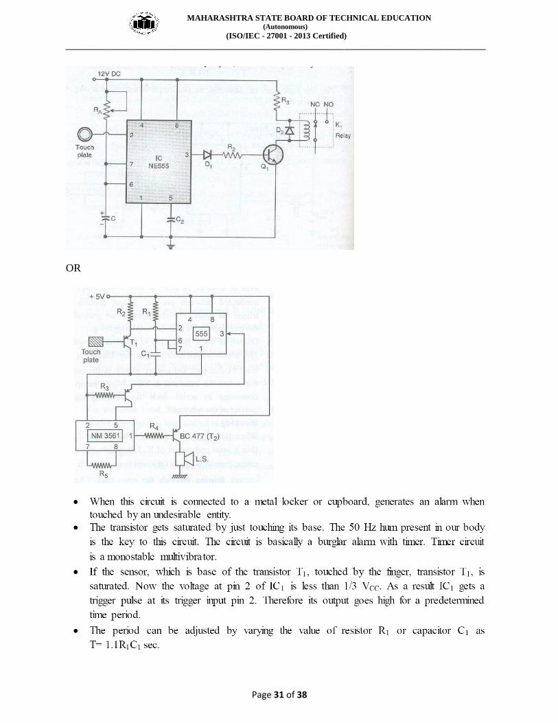
f) Describe the application of IC 555 as touch plate switch with circuit diagram.
Ans:-( Diagram- 2 mks, description-2 mks)
MAHARASHTRA STATE BOARD OF TECHNICAL EDUCATION (Autonomous)
(ISO/IEC - 27001 - 2013 Certified)
____________________________________________________________________________________________
Page 31 of 38
OR
MAHARASHTRA STATE BOARD OF TECHNICAL EDUCATION (Autonomous)
(ISO/IEC - 27001 - 2013 Certified)
____________________________________________________________________________________________
Page 32 of 38
6. Attempt any FOUR of the following: Marks 16
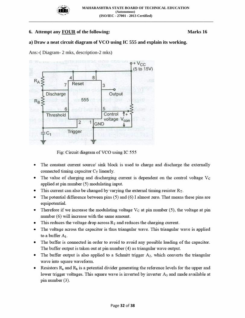
a) Draw a neat circuit diagram of VCO using IC 555 and explain its working.
Ans:-( Diagram- 2 mks, description-2 mks)
MAHARASHTRA STATE BOARD OF TECHNICAL EDUCATION (Autonomous)
(ISO/IEC - 27001 - 2013 Certified)
____________________________________________________________________________________________
Page 33 of 38
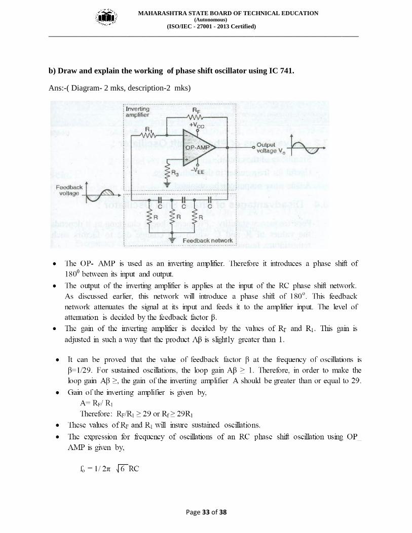
b) Draw and explain the working of phase shift oscillator using IC 741.
Ans:-( Diagram- 2 mks, description-2 mks)
MAHARASHTRA STATE BOARD OF TECHNICAL EDUCATION (Autonomous)
(ISO/IEC - 27001 - 2013 Certified)
____________________________________________________________________________________________
Page 34 of 38
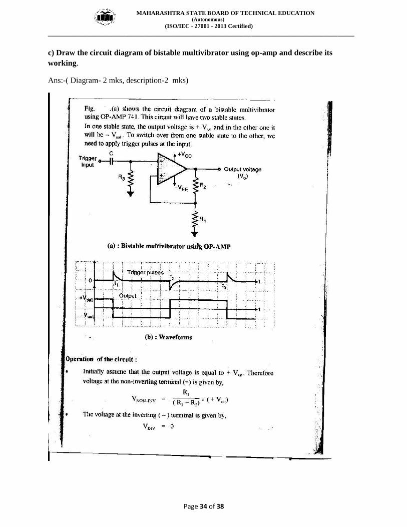
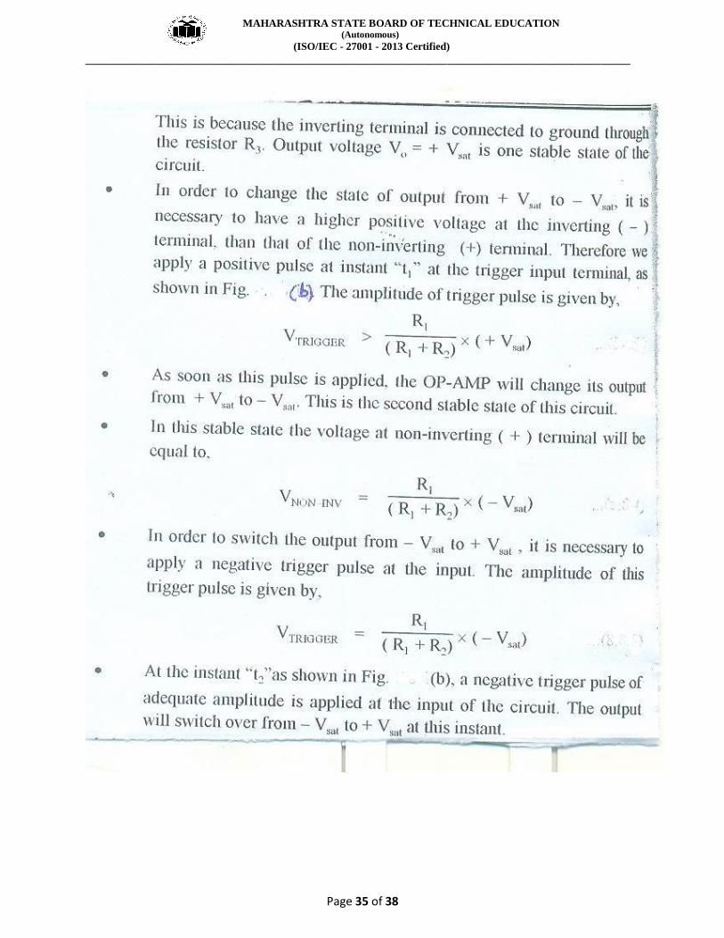
c) Draw the circuit diagram of bistable multivibrator using op-amp and describe its
working.
Ans:-( Diagram- 2 mks, description-2 mks)
MAHARASHTRA STATE BOARD OF TECHNICAL EDUCATION (Autonomous)
(ISO/IEC - 27001 - 2013 Certified)
____________________________________________________________________________________________
Page 35 of 38
MAHARASHTRA STATE BOARD OF TECHNICAL EDUCATION (Autonomous)
(ISO/IEC - 27001 - 2013 Certified)
____________________________________________________________________________________________
Page 36 of 38
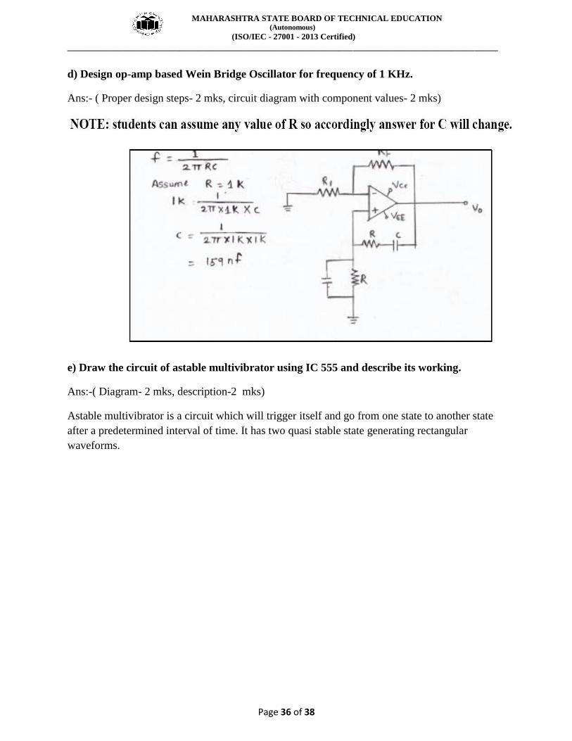
d) Design op-amp based Wein Bridge Oscillator for frequency of 1 KHz.
Ans:- ( Proper design steps- 2 mks, circuit diagram with component values- 2 mks)
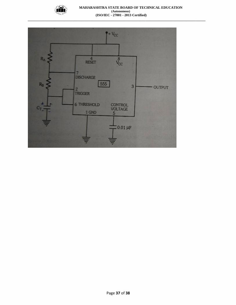
e) Draw the circuit of astable multivibrator using IC 555 and describe its working.
Ans:-( Diagram- 2 mks, description-2 mks)
Astable multivibrator is a circuit which will trigger itself and go from one state to another state
after a predetermined interval of time. It has two quasi stable state generating rectangular
waveforms.
MAHARASHTRA STATE BOARD OF TECHNICAL EDUCATION (Autonomous)
(ISO/IEC - 27001 - 2013 Certified)
____________________________________________________________________________________________
Page 37 of 38
MAHARASHTRA STATE BOARD OF TECHNICAL EDUCATION (Autonomous)
(ISO/IEC - 27001 - 2013 Certified)
____________________________________________________________________________________________
Page 38 of 38
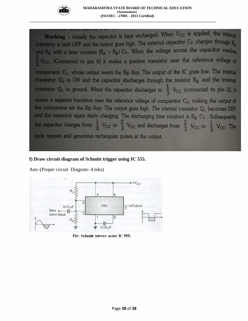
f) Draw circuit diagram of Schmitt trigger using IC 555.
Ans:-(Proper circuit Diagram- 4 mks)