Embed Size (px)
Citation preview
Abstract : Reconfigurable Computing : Wiley Encyclopedia of Electric... http://www.mrw.interscience.wiley.com/emrw/9780471346081/eeee/ar...
1 of 1 7/9/2007 2:38 PM
My Profile Log In
Recommend toYour LibrarianSave title to MyProfileEmail this pagePrint this page
HOMEABOUT USCONTACT USHELP
Home / Engineering / Electrical and Electronics Engineering
Wiley Encyclopedia of Electrical and ElectronicsEngineering
Reconfigurable ComputingStandard Article
Cheng Chung-Kuan1, Andrew B. Kahng2, Philip H.W. Leong2
1Dept. of Computer Science and Engineering,University of California, La Jolla, California
2Dept. of Computer Science and Engineering, TheChinese University of Hong Kong, Shatin, Hong Kong
Copyright © 2007 by John Wiley & Sons, Inc. All rightsreserved.DOI: 10.1002/047134608X.W7603.pub2Article Online Posting Date: June 15, 2007
Abstract | Full Text: HTML PDF (1550K)
BROWSE THIS TITLEArticle Titles A–ZTopics
SEARCH THIS TITLE
Advanced Product SearchSearch All ContentAcronym Finder
AbstractReconfigurable computing is the application of adaptable fabrics to solve computational problems, oftentaking advantage the flexibility available in the fabric to produce problem-specific architectures thatachieve high performance because of customization. Reconfigurable computing has been successfullyapplied to fields as diverse as digital signal processing, cryptography, bioinformatics, logic emulation, CADtool acceleration, scientific computing, and rapid prototyping.
Although Estrin-first proposed the idea of a reconfigurable system in the form of a fixed plus variablestructure computer in 1960 (1) it has only been in recent years that reconfigurable fabrics have reachedsufficient density to make them a compelling implementation platform for high Performance applicationsand embedded systems. In this article, intended for the non-specialist, we describe some of the basicconcepts, tools and architectures associated with reconfigurable computing.
Keywords: reconfigurable computing; adaptable fabrics; application integrated circuits; fieldprogrammable gate arrays (fpgas); system architecture; runtime
About Wiley InterScience | About Wiley | Privacy | Terms & ConditionsCopyright © 1999-2007John Wiley & Sons, Inc. All Rights Reserved.
RECONFIGURABLE COMPUTING
INTRODUCTION
Although reconfigurable fabrics can in principle be con-structed from any type of technology, in practice, most con-temporary designs are made using commercial field pro-grammable gate arrays (FPGAs). An FPGA is an inte-grated circuit containing an array of logic gates in whichthe connections can be configured by downloading a bit-stream to its memory. FPGAs can also be embedded in in-tegrated circuits as intellectual property cores. More de-tailed surveys on reconfigurable computing are availablein the literature (2–5).
Microprocessors offer an easy-to-use, powerful, and flex-ible implementation medium for digital systems. Theirutility in computing applications makes them an over-whelming first choice, and parallel interconnections of mi-croprocessors can be extremely powerful. Moreover, it isrelatively easy to find software developers, and micropro-cessors are widely supported by operating systems, soft-ware engineering tools, and libraries. Unfortunately, theirgenerality does not make them the best choice for a largeclass of applications that need to be optimized for perfor-mance, power, board area.
Application-specific integrated circuits (ASICs) and FP-GAs are able to arrange computations in a spatial ratherthan temporal fashion and greater levels of parallelismthan a microprocessor can be achieved. Thus, perfor-mance improvements of several orders of magnitude canbe achieved. Also, the absence of caches and instruction de-coding can result in the same amount of work being donewith less chip area and lower power consumption (6). As anexample, in a cryptographic key search problem, a singleFPGA with 96 parallel RC4 encryption engines operatingat 50 MHz achieved a speedup of 58 over a 1.5-GHz Pen-tium 4 implementation (7).
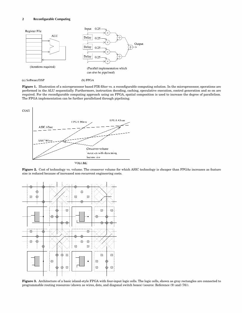
An example involving the implementation of a finite im-pulse response (FIR) filter is shown in Fig. 1. The recon-figurable computing solution is significantly more parallelthan the microprocessor-based one. In addition, it shouldbe apparent that the reconfigurable solution avoids theoverheads associated with instruction decoding, caching,register files, and speculative execution, and unnecessarydata transfers as well as control hardware can be omitted.
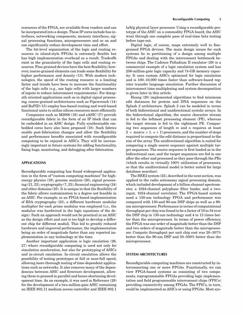
Compared with ASICs, FPGAs offer very low non-recurrent engineering (NRE) costs, which is often a moreimportant factor than the fact that FPGAs have higherunits costs and many applications do not have the very highvolumes required to make ASICs a cheaper proposition. Asintegrated circuit feature sizes continue to decrease, theNRE costs associated with ASICs continue to escalate, in-creasing the volume at which it becomes cheaper to use anASIC (see Fig. 2). Reconfigurable computing will be usedin increasingly more applications, as ASICs become onlycost effective for the highest performance or highest vol-ume applications.
Additional benefits of reconfigurable computing are thatits technology provides a shorter time to market than
ASICs (associated FPGA fabrication time is essentiallyzero), making many fabrication iterations within a sin-gle day possible. This benefit allows more complex algo-rithms to be deployed and makes possible problem-specificcustomizations of designs. FPGA-based designs are inher-ently less risky in terms of technical feasibility and cost, asshorter design times and lower upfront costs are involved.As its name suggests, FPGAs also offer the possibility ofmodifications to the design in the field, which can be used toprovide bug fixes, modifications to adapt to changing stan-dards, or to add functionality, all of which can be achievedby downloading a new bitstream to an existing reconfig-urable computing platform. Reconfiguration can even takeplace while the system is running, this being known as run-time reconfiguration [e.g., (8)]. Runtime reconfiguration isexplained in more detail later in this article.
In the next section, we introduce the basic architectureof common reconfigurable fabrics, followed by a discussionof applications of reconfigurable computing and system ar-chitectures. Runtime reconfiguration and design methodsare then covered. Finally,we discuss multichip systems andend with a conclusion.
RECONFIGURABLE FABRICS
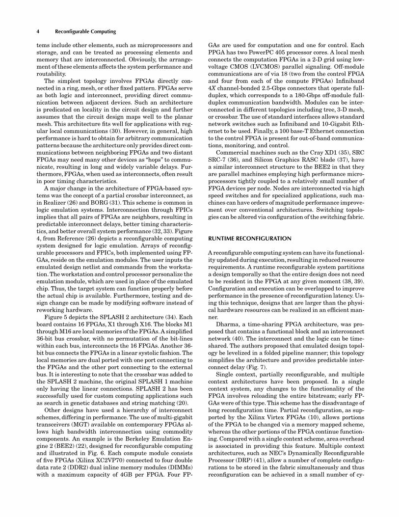
A block diagram illustrating a generic fine-grained island-style FPGA is given in Fig. 3 (9). Products from companiessuch as Xilinx (10) Altera (11), and Actel (12) are commer-cial examples. The FPGA consists of a number of logic cellsthat can be interconnected to other logic and input/output(I/O) cells via programmable routing resources. Logic cellsand routing resources are configured via bit-level program-ming data, which is stored in memory cells in the FPGA.A logic cell consists of user-programmable combinatorialelements, with an optional register at the output. They areoften implemented as lookup tables (LUTs) with a smallnumber of inputs, 4-input LUTs being shown in Fig. 3. Us-ing such an architecture, subject to FPGA-imposed limita-tions on the circuit’s speed and density, an arbitrary circuitcan be implemented. The complete design is described viathe configuration bitstream which specifies the logic andI/O cell functionality, and their interconnection.
Current trends are to incorporate additional embeddedblocks so that designers can integrate entire systems ona single FPGA device. Apart from density, cost, and boardarea benefits, this process also improves performance be-cause more specialized logic and routing can be used andall components are on the same chip. A contemporaryFPGA commonly has features such as carry chains to en-able fast addition; wide decoders; tristate buffers; blocksof on-chip memory and multipliers; embedded micropro-cessors; programmable I/O standards in the input/outputcells; delay locked loops; phase locked loops for clock de-skewing, phase shifting and multiplication; multi-gigabittransceivers (MGTs); and embedded microprocessors. Em-bedded microprocessors can be implemented either as softcores using the internal FPGA resources or as hardwiredcores.
In addition to the architectural features described, intel-lectual property (IP) cores, implemented using the logic cell
J. Webster (ed.), Wiley Encyclopedia of Electrical and Electronics Engineering. Copyright © 2007 John Wiley & Sons, Inc.
2 Reconfigurable Computing
Figure 1. Illustration of a microprocessor based FIR filter vs. a reconfigurable computing solution. In the microprocessor, operations areperformed in the ALU sequentially. Furthermore, instruction decoding, caching, speculative execution, control generation and so on arerequired. For the reconfigurable computing approach using an FPGA, spatial composition is used to increase the degree of parallelism.The FPGA implementation can be further parallelized through pipelining.
Figure 2. Cost of technology vs. volume. The crossover volume for which ASIC technology is cheaper than FPGAs increases as featuresize is reduced because of increased non-recurrent engineering costs.
Figure 3. Architecture of a basic island-style FPGA with four-input logic cells. The logic cells, shown as gray rectangles are connected toprogrammable routing resources (shown as wires, dots, and diagonal switch boxes) (source: Reference (9) and (76)).
Reconfigurable Computing 3
resources of the FPGA, are available from vendors and canbe incorporated into a design.These IP cores include bus in-terfaces, networking components, memory interfaces, sig-nal processing functions, microprocessors and so on andcan significantly reduce development time and effort.
The bit-level organization of the logic and routing re-sources in island-style FPGAs is extremely flexible buthas high implementation overhead as a result. Tradeoffsexist in the granularity of the logic cells and routing re-sources. Fine-grained devices have the best flexibility; how-ever, coarse-grained elements can trade some flexibility forhigher performance and density (13). With modern tech-nologies, the speed of the routing resource is a limitingfactor and trends have been to increase the functionalityof the logic cells (e.g., use logic cells with larger numbersof inputs to reduce interconnect requirements). For datap-ath oriented applications such as in digital signal process-ing, coarse-grained architectures such as Pipewrench (14)and RaPID (15) employ bus-based routing and word-basedfunctional units to utilize silicon resources more efficiently.
Companies such as M2000 (16) and eASIC (l7) providereconfigurable fabric in the form of an IP block that canbe embedded in an ASIC design. Fully synthesizable em-bedded cores have also been proposed (18). Such fabricsenable post-fabrication changes and allow the flexibilityand performance benefits associated with reconfigurablecomputing to be enjoyed in ASICs. They will be increas-ingly important in future systems for adding functionality,fixing bugs, monitoring, and debugging after fabrication.
APPLICATIONS
Reconfigurable computing has found widespread applica-tion in the form of “custom computing-machines” for high-energy physics (19), genome analysis (20), signal process-ing (21, 22), cryptography (7, 23), financial engineering (24)and other domains (25). It is unique in that the flexibility ofthe fabric allows customization to a degree not feasible inan ASIC. For example, in an FPGA-based implementationof RSA cryptography (23), a different hardware modularmultiplier for each prime modulus was employed (i.e., themodulus was hardwired in the logic equations of the de-sign). Such an approach would not be practical in an ASICas the design effort and cost is too high to develop a differ-ent chip for different moduli. This led to greatly reducedhardware and improved performance, the implementationbeing an order of magnitude faster than any reported im-plementation in any technology at the time.
Another important application is logic emulation (26,27) where reconfigurable computing is used not only forsimulation acceleration, but also for prototyping of ASICsand in-circuit emulation. In-circuit emulation allows thepossibility of testing prototypes at full or near-full speed,allowing more thorough testing of time-dependent applica-tions such as networks. It also removes many of the depen-dencies between ASIC and firmware development, allow-ing them to proceed in parallel and hence shortening devel-opment time. As an example, it was used in Reference (28)for the development of a two-million-gate ASIC containingan IEEE 802.11 medium access controller and IEEE 802.1
la/b/g physical layer processor. Using a reconfigurable pro-totype of the ASIC on a commodity FPGA board, the ASICwent through one complete pass of real-time beta testingbefore tape-out.
Digital logic, of course, maps extremely well to fine-grained FPGA devices. The main design issues for suchsystems lie in partitioning of a design among multipleFPGAs and dealing with the interconnect bottleneck be-tween chips. The Cadence Palladium II emulator (29) is acommercial example of a logic emulation system and has256-million-gate logic capacity and 74-GB memory capac-ity. It uses custom ASICs optimized for logic emulationand is 100–10,000 times faster than software-based reg-ister transfer language simulation. Further discussion ofinterconnect time-multiplexing and system decompositionis given later in this article.
Hoang (20) implemented algorithms to find minimumedit distances for protein and DNA sequences on theSplash 2 architecture. Splash 2 can be modeled in termsof both bidirectional and unidirectional systolic arrays. Inthe bidirectional algorithm, the source character streamis fed to the leftmost processing element (PE), whereasthe target stream is fed to the rightmost PE. Compar-ing two sequences of length m and n requires at least2 × max(m + 1, n + 1) processors, and the number of stepsrequired to compute the edit distance is proportional to thesize of the array. The unidirectional algorithm is suited forcomparing a single source sequence against multiple tar-get sequences. The source sequence is first loaded as in thebidirectional case, and the target sequences are fed in oneafter the other and processed as they pass through the PEs(which results in virtually 100% utilization of processors,so that the unidirectional model is better suited for largedatabase searches).
The BEE2 system (22),described in the next section,wasapplied to the radio astronomy signal processing domain,which included development of a billion-channel spectrom-eter, a 1024-channel polyphase filter banks, and a two-input, 1024-channel correlator. The FPGA-based systemused a 130-nm technology FPGA and performance wascompared with 130-and 90-nm DSP chips as well as a 90-nm microprocessor. Performance in terms of computationalthroughput per chip was found to be a factor of 10 to 34 overthe DSP chip in 130-nm technology and 4 to 13 times bet-ter than the microprocessor. In terms of power efficiency,the FPGA was one order of magnitude better than the DSPand two orders of magnitude better than the microproces-sor. Compute throughput per unit chip cost was 20–307%better than the 90-nm DSP and 50–500% better than themicroprocessor.
SYSTEM ARCHITECTURES
Reconfigurable computing machines are constructed by in-terconnecting one or more FPGAs. Functionally, we canview FPGA-based systems as consisting of two compo-nents, reprogrammable FPGAs providing logic implemen-tation and field programmable interconnect chips (FPICs)providing connectivity among FPGAs. The FPICs, in turn,could be implemented as ASICs or using FPGAs. Most sys-
4 Reconfigurable Computing
tems include other elements, such as microprocessors andstorage, and can be treated as processing elements andmemory that are interconnected. Obviously, the arrange-ment of these elements affects the system performance androutability.
The simplest topology involves FPGAs directly con-nected in a ring, mesh, or other fixed pattern. FPGAs serveas both logic and interconnect, providing direct commu-nication between adjacent devices. Such an architectureis predicated on locality in the circuit design and furtherassumes that the circuit design maps well to the planarmesh. This architecture fits well for applications with reg-ular local communications (30). However, in general, highperformance is hard to obtain for arbitrary communicationpatterns because the architecture only provides direct com-munications between neighboring FPGAs and two distantFPGAs may need many other devices as “hops” to commu-nicate, resulting in long and widely variable delays. Fur-thermore, FPGAs, when used as interconnects, often resultin poor timing characteristics.
A major change in the architecture of FPGA-based sys-tems was the concept of a partial crossbar interconnect, asin Realizer (26) and BORG (31). This scheme is common inlogic emulation systems. Interconnection through FPICsimplies that all pairs of FPGAs are neighbors, resulting inpredictable interconnect delays, better timing characteris-tics, and better overall system performance (32, 33). Figure4, from Reference (26) depicts a reconfigurable computingsystem designed for logic emulation. Arrays of reconfig-urable processors and FPICs, both implemented using FP-GAs, reside on the emulation modules. The user inputs theemulated design netlist and commands from the worksta-tion. The workstation and control processor personalize theemulation module, which are used in place of the emulatedchip. Thus, the target system can function properly beforethe actual chip is available. Furthermore, testing and de-sign change can be made by modifying software instead ofreworking hardware.
Figure 5 depicts the SPLASH 2 architecture (34). Eachboard contains 16 FPGAs, X1 through X16. The blocks M1through M16 are local memories of the FPGAs. A simplified36-bit bus crossbar, with no permutation of the bit-lineswithin each bus, interconnects the 16 FPGAs. Another 36-bit bus connects the FPGAs in a linear systolic fashion. Thelocal memories are dual ported with one port connecting tothe FPGAs and the other port connecting to the externalbus. It is interesting to note that the crossbar was added tothe SPLASH 2 machine, the original SPLASH 1 machineonly having the linear connections. SPLASH 2 has beensuccessfully used for custom computing applications suchas search in genetic databases and string matching (20).
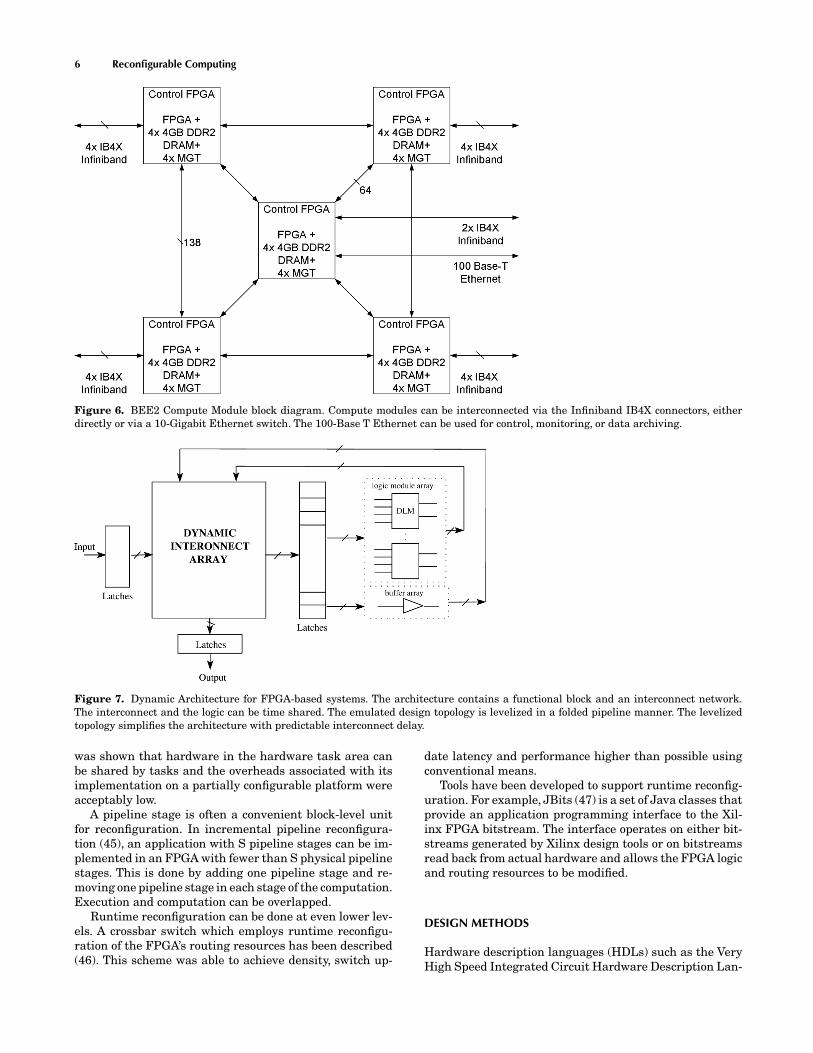
Other designs have used a hierarchy of interconnectschemes, differing in performance. The use of multi-gigabittransceivers (MGT) available on contemporary FPGAs al-lows high bandwidth interconnection using commoditycomponents. An example is the Berkeley Emulation En-gine 2 (BEE2) (22), designed for reconfigurable computingand illustrated in Fig. 6. Each compute module consistsof five FPGAs (Xilinx XC2VP70) connected to four doubledata rate 2 (DDR2) dual inline memory modules (DIMMs)with a maximum capacity of 4GB per FPGA. Four FP-
GAs are used for computation and one for control. EachPPGA has two PowerPC 405 processor cores. A local meshconnects the computation FPGAs in a 2-D grid using low-voltage CMOS (LVCMOS) parallel signaling. Off-modulecommunications are of via 18 (two from the control FPGAand four from each of the compute FPGAs) Infiniband4X channel-bonded 2.5-Gbps connectors that operate full-duplex, which corresponds to a 180-Gbps off-module full-duplex communication bandwidth. Modules can be inter-connected in different topologies including tree, 3-D mesh,or crossbar. The use of standard interfaces allows standardnetwork switches such as Infiniband and 10-Gigabit Eth-ernet to be used. Finally, a 100 base-T Ethernet connectionto the control FPGA is present for out-of-band communica-tions, monitoring, and control.
Commercial machines such as the Cray XD1 (35), SRCSRC-7 (36), and Silicon Graphics RASC blade (37), havea similar interconnect structure to the BEE2 in that theyare parallel machines employing high performance micro-processors tightly coupled to a relatively small number ofFPGA devices per node. Nodes are interconnected via highspeed switches and for specialized applications, such ma-chines can have orders of magnitude performance improve-ment over conventional architectures. Switching topolo-gies can be altered via configuration of the switching fabric.
RUNTIME RECONFIGURATION
A reconfigurable computing system can have its functional-ity updated during execution, resulting in reduced resourcerequirements. A runtime reconfigurable system partitionsa design temporally so that the entire design does not needto be resident in the FPGA at any given moment (38, 39).Configuration and execution can be overlapped to improveperformance in the presence of reconfiguration latency. Us-ing this technique, designs that are larger than the physi-cal hardware resources can be realized in an efficient man-ner.
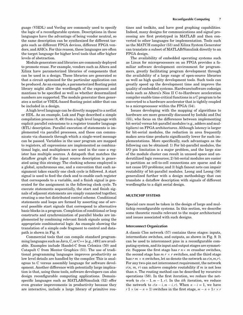
Dharma, a time-sharing FPGA architecture, was pro-posed that contains a functional block and an interconnectnetwork (40). The interconnect and the logic can be time-shared. The authors proposed that emulated design topol-ogy be levelized in a folded pipeline manner; this topologysimplifies the architecture and provides predictable inter-connect delay (Fig. 7).
Single context, partially reconfigurable, and multiplecontext architectures have been proposed. In a singlecontext system, any changes to the functionality of theFPGA involves reloading the entire bitstream; early FP-GAs were of this type. This scheme has the disadvantage oflong reconfiguration time. Partial reconfiguration, as sup-ported by the Xilinx Virtex FPGAs (10), allows portionsof the FPGA to be changed via a memory mapped scheme,whereas the other portions of the FPGA continue function-ing. Compared with a single context scheme, area overheadis associated in providing this feature. Multiple contextarchitectures, such as NEC’s Dynamically ReconfigurableProcessor (DRP) (41), allow a number of complete configu-rations to be stored in the fabric simultaneously and thusreconfiguration can be achieved in a small number of cy-
Reconfigurable Computing 5
Figure 4. Example of a logic emulation system. Arrays ofFPGAs and FPICs reside on the emulation modules. The user inputs theemulated design netlist and commands from the workstation. The workstation and control processor personalize the emulation modules,which are used in place of the emulated chip.
Figure 5. SPLASH2 architecture. Each board contains 16 FPGAs, XI through XI6. The blocks Ml through Ml6 are local memories of theFPGAs. A simplified 36-bit bus crossbar, with no permutation of the bit-lines within each bus, interconnects the 16 FPGAs. Another 36-bitbus connects the FPGAs in daisy-chain fashion. The local memories are dual ported with one port connecting to the FPGAs and the otherport connecting to the external bus.
cles. This architecture has the shortest context switch time,however, a larger area overhead is associated with imple-mentation of this scheme.
The logical unit of reconfiguration could be at a num-ber of levels including the application, instruction, task,block, or sub-block level. An example of application-levelreconfiguration could simply involve loading a runtime-dependent bitstream to support a particular coding stan-dard in a video coding application. The Dynamic Instruc-tion Set Computer (DISC) (42) supported demand-drivenmodification of the instruction set through partial reconfig-uration. The commercial Stretch processor (43) combines
reconfigurable fabric with a processor to support the exe-cution of custom instructions implemented on a reconfig-urable fabric. Furthermore, the fabric can be reconfiguredat runtime and the design environment is software-centric,with programming of the processor being in Stretch C.
An operating system for guarantee-based scheduling ofhard real-time tasks has been proposed (44). Under controlof software running on a microprocessor, task circuits canbe scheduled online and placed in a suitable free space in ahardware task area. Communications between tasks andI/O are done though a task communication bus, and termi-nation of a task frees the reconfigurable resources used. It
6 Reconfigurable Computing
Figure 6. BEE2 Compute Module block diagram. Compute modules can be interconnected via the Infiniband IB4X connectors, eitherdirectly or via a 10-Gigabit Ethernet switch. The 100-Base T Ethernet can be used for control, monitoring, or data archiving.
Figure 7. Dynamic Architecture for FPGA-based systems. The architecture contains a functional block and an interconnect network.The interconnect and the logic can be time shared. The emulated design topology is levelized in a folded pipeline manner. The levelizedtopology simplifies the architecture with predictable interconnect delay.
was shown that hardware in the hardware task area canbe shared by tasks and the overheads associated with itsimplementation on a partially configurable platform wereacceptably low.
A pipeline stage is often a convenient block-level unitfor reconfiguration. In incremental pipeline reconfigura-tion (45), an application with S pipeline stages can be im-plemented in an FPGA with fewer than S physical pipelinestages. This is done by adding one pipeline stage and re-moving one pipeline stage in each stage of the computation.Execution and computation can be overlapped.
Runtime reconfiguration can be done at even lower lev-els. A crossbar switch which employs runtime reconfigu-ration of the FPGA’s routing resources has been described(46). This scheme was able to achieve density, switch up-
date latency and performance higher than possible usingconventional means.
Tools have been developed to support runtime reconfig-uration. For example, JBits (47) is a set of Java classes thatprovide an application programming interface to the Xil-inx FPGA bitstream. The interface operates on either bit-streams generated by Xilinx design tools or on bitstreamsread back from actual hardware and allows the FPGA logicand routing resources to be modified.
DESIGN METHODS
Hardware description languages (HDLs) such as the VeryHigh Speed Integrated Circuit Hardware Description Lan-
Reconfigurable Computing 7
guage (VHDL) and Verilog are commonly used to specifythe logic of a reconfigurable system. Descriptions in theselanguages have the advantage of being vendor neutral, sothe same description can be synthesized for different tar-gets such as different FPGA devices, different FPGA ven-dors, and ASICs. For this reason, these languages are oftenthe target language for higher level tools that offer higherlevels of abstraction.
Module generators and libraries are commonly deployedto promote reuse. For example, vendors such as Altera andXilinx have parameterized libraries of components thatcan be used in a design. These libraries are generated sothat a circuit optimized for the particular application canbe produced. As an example, a parameterized floating pointlibrary might allow the wordlength of the exponent andmantissa to be specified as well as whether denormalizednumbers are supported. The module generator then gener-ates a netlist or VHDL-based floating point adder that canbe included in a design.
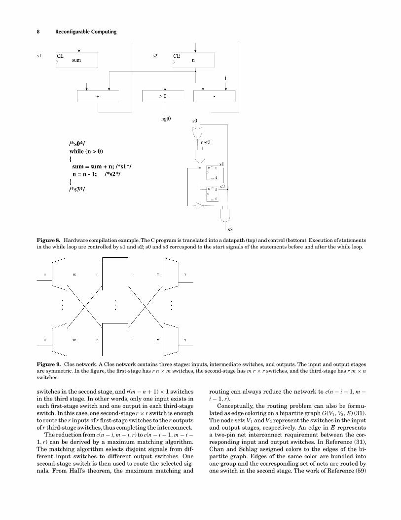
A high level language can be directly mapped to a netlistor HDL. As an example, Luk and Page described a simplecompilation process (8, 49) from a high level language withexplicit parallel extensions to a register transfer language(RTL) description. Parallel execution of statements is im-plemented via parallel processes, and these can commu-nicate via channels through which a single-word messagecan be passed. Variables in the user program are mappedto registers, all expressions are implemented as combina-tional logic, and multiplexers are used in the case a reg-ister has multiple sources. A datapath that matches thedataflow graph of the input source description is gener-ated using this strategy. The clocking scheme employed isa global, synchronous one, and a convention that each as-signment takes exactly one clock cycle is followed. A startsignal is used to feed the clock and to enable each registerthat corresponds to a variable, and a finish signal is gen-erated for the assignment in the following clock cycle. Toexecute statements sequentially, the start and finish sig-nals of adjacent statements are simply connected together,creating a one-hot distributed control scheme. Conditionalstatements and loops are formed by asserting one of sev-eral possible start signals that correspond to alternativebasic blocks in a program. Completion of conditional or loopconstructs and synchronization of parallel blocks are im-plemented by combining relevant finish signals using theappropriate combinatorial logic. An example showing thetranslation of a simple code fragment to control and data-path is shown in Fig. 8.
Commercial tools that can compile standard program-ming languages such as Java, C, or C++ [e.g., (49)] are avail-able. Examples include Handel-C from Celoxica (50) andCatapult C from Mentor Graphics (51). The use of tradi-tional programming languages improves productivity aslow level details are handled by the compiler. This is anal-ogous to C versus assembly language for software devel-opment. Another difference with potentially large implica-tion is that, using these tools, software developers can alsodesign reconfigurable computing applications. Domain-specific languages such as MATLAB/Simulink (52) offereven greater improvements in productivity because theyare interactive, include a large library of primitive rou-
tines and toolkits, and have good graphing capabilities.Indeed, many designs for communications and signal pro-cessing are first prototyped in MATLAB and then con-verted to other languages for implementation. Tools suchas the MATCH compiler (53) and Xilinx System Generatorcan translate a subset of MATLAB/Simulink directly to anFPGA design.
The availability of embedded operating systems suchas Linux for microprocessors on an FPGA provides a fa-miliar software development environment for program-mers, greatly facilitating program development throughthe availability of a large range of open-source librariesas well as high quality development tools. Such tools cangreatly speed up the development time and improve thequality of embedded systems. Hardware/software codesigntools such as Altera’s Nios II C-to-Hardware accelerationcompiler enable time-critical functions in a C program to beconverted to a hardware accelerator that is tightly coupledto a microprocessor within the FPGA (54).
Issues developing with the mapping of algorithms tohardware are more generally discussed by Isshiki and Dai(55), who focus on the differences between implementingbit-serial versus bit-parallel modules (e.g., adders and mul-tipliers) on FPGA architectures. Although latency is largerfor bit-serial modules, the reduction in area frequentlymakes area-time products significantly lower for such im-plementations. More specifically, such advantages as thefollowing can be obtained: 1) For bit-parallel modules, theI/O pin limitation is a major problem, and the large sizeof the module cluster can result in unused space and un-derutilized logic resources; 2) bit-serial modules are easierto partition as cell-to-cell connections are sparse and donot cause I/O problems; and 3) high fanout nets can impairroutability of bit-parallel modules. Leong and Leong (56)generalized further with a design methodology that cantranslate a dataflow description with signals of differentwordlengths to a digit serial design.
MULTICHIP SYSTEMS
Special care must be taken in the design of large and mul-tichip reconfigurable systems. In this section, we describesome theoretic results relevant to the major architecturaland issues associated with such designs.
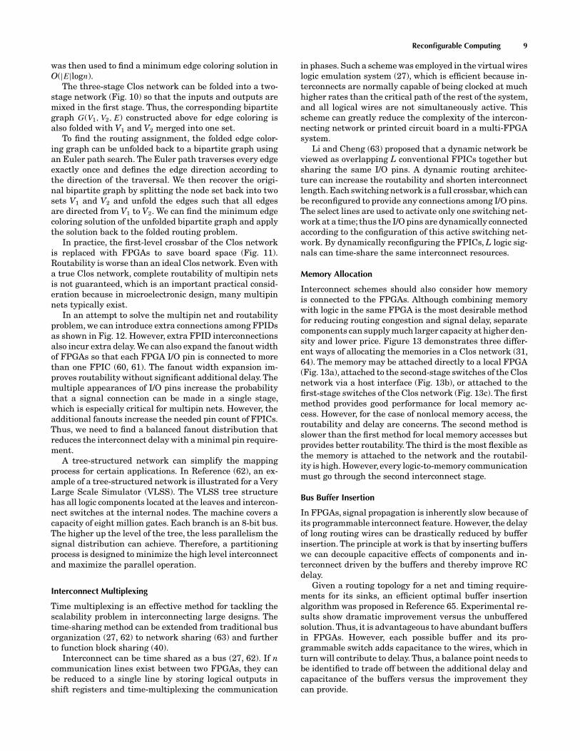
Interconnect Organization
A classic Clos network (57) contains three stages: inputs,intermediate switches, and outputs, as shown in Fig. 9. Itcan be used to interconnect pins in a reconfigurable com-puting system,and its input and output stages are symmet-ric. Suppose the first stage has r n× m crossbar switches,the second stage has m r × r switches, and the third stagehas r m × n switches, let us denote the network as c(n,m,r).For any two-pin net interconnect requirement, the networkc(n, m, r) can achieve complete routability if m is not lessthan n. The routing method can be described by recursiveoperations (58). In the first iteration, we reduce the net-work to c(n − 1, m − 1, r). In the ith iteration, we reducethe network to c(n − i, m − i, r). When n − i = 1, we haver 1 × (m − n + 1) switches in the first stage, m − n + 1 r × r
8 Reconfigurable Computing
Figure 8. Hardware compilation example. The C program is translated into a datapath (top) and control (bottom). Execution of statementsin the while loop are controlled by s1 and s2; s0 and s3 correspond to the start signals of the statements before and after the while loop.
Figure 9. Clos network. A Clos network contains three stages: inputs, intermediate switches, and outputs. The input and output stagesare symmetric. In the figure, the first-stage has r n × m switches, the second-stage has m r × r switches, and the third-stage has r m × nswitches.
switches in the second stage, and r(m − n + 1) × 1 switchesin the third stage. In other words, only one input exists ineach first-stage switch and one output in each third-stageswitch. In this case, one second-stage r × r switch is enoughto route the r inputs of r first-stage switches to the r outputsof r third-stage switches, thus completing the interconnect.
The reduction from c(n − i, m − i, r) to c(n − i − 1, m − i −1, r) can be derived by a maximum matching algorithm.The matching algorithm selects disjoint signals from dif-ferent input switches to different output switches. Onesecond-stage switch is then used to route the selected sig-nals. From Hall’s theorem, the maximum matching and
routing can always reduce the network to c(n − i − 1, m −i − 1, r).
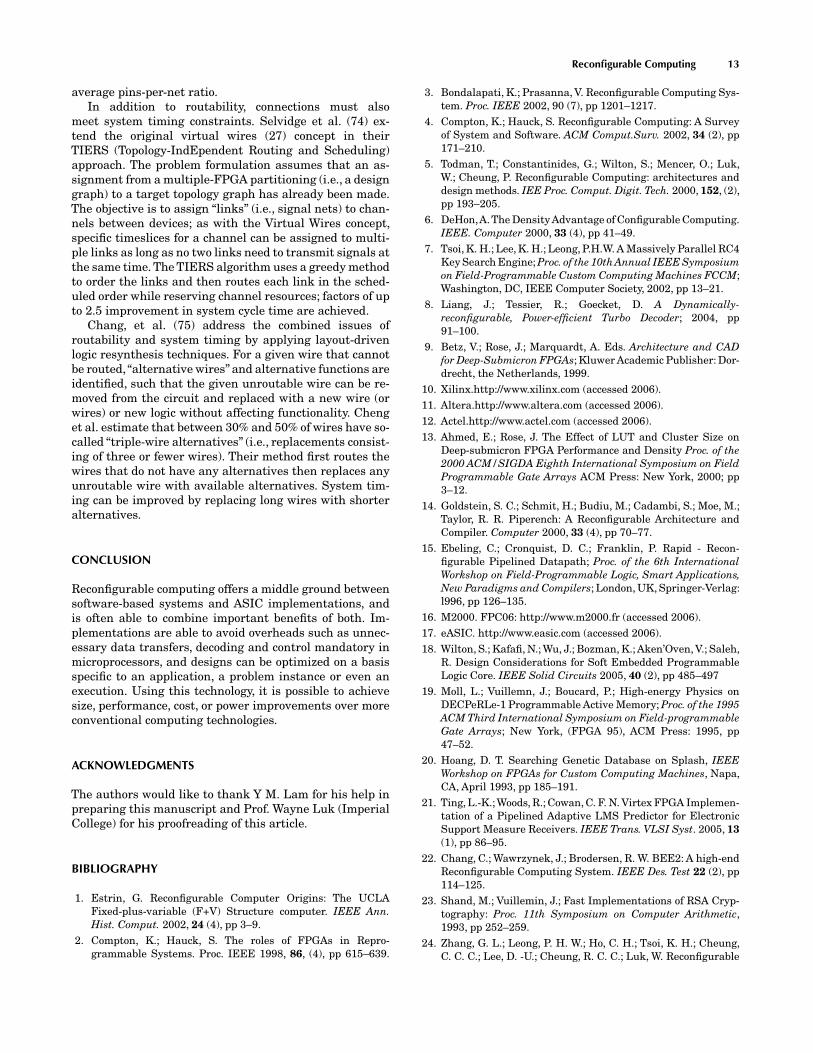
Conceptually, the routing problem can also be formu-lated as edge coloring on a bipartite graph G(V1, V2, E) (31).The node sets V1 and V2 represent the switches in the inputand output stages, respectively. An edge in E representsa two-pin net interconnect requirement between the cor-responding input and output switches. In Reference (31),Chan and Schlag assigned colors to the edges of the bi-partite graph. Edges of the same color are bundled intoone group and the corresponding set of nets are routed byone switch in the second stage. The work of Reference (59)
Reconfigurable Computing 9
was then used to find a minimum edge coloring solution inO(|E|logn).
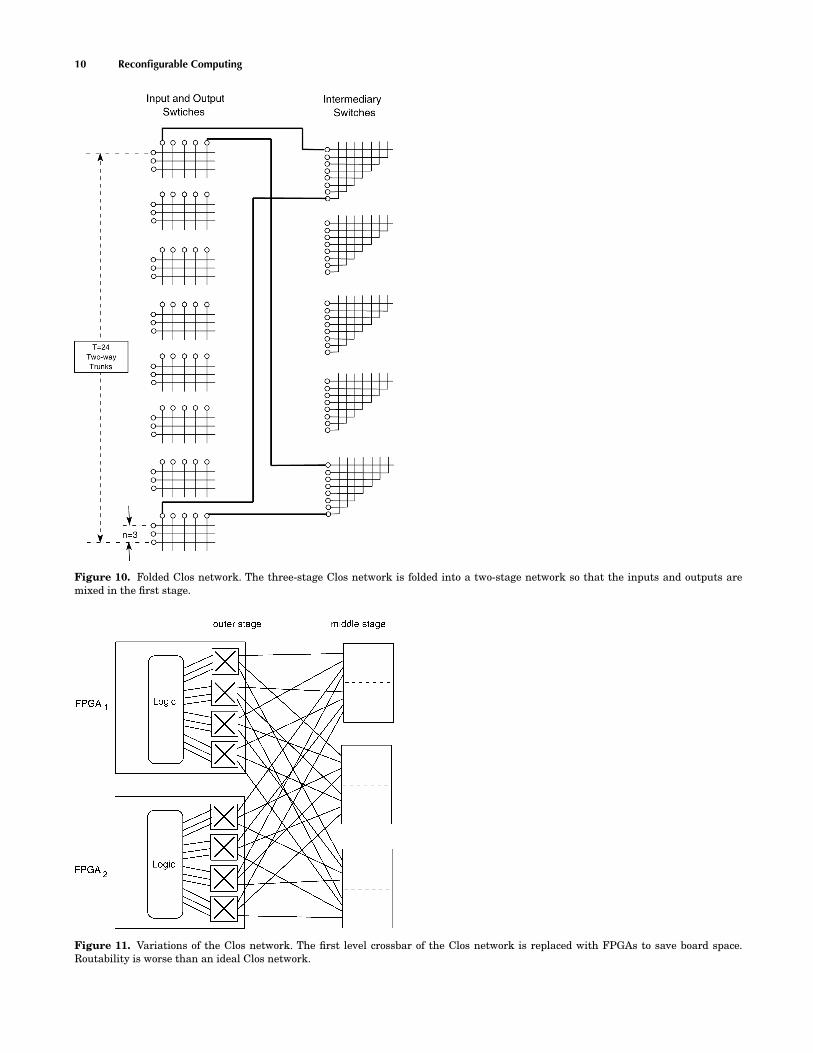
The three-stage Clos network can be folded into a two-stage network (Fig. 10) so that the inputs and outputs aremixed in the first stage. Thus, the corresponding bipartitegraph G(V1, V2, E) constructed above for edge coloring isalso folded with V1 and V2 merged into one set.
To find the routing assignment, the folded edge color-ing graph can be unfolded back to a bipartite graph usingan Euler path search. The Euler path traverses every edgeexactly once and defines the edge direction according tothe direction of the traversal. We then recover the origi-nal bipartite graph by splitting the node set back into twosets V1 and V2 and unfold the edges such that all edgesare directed from V1 to V2. We can find the minimum edgecoloring solution of the unfolded bipartite graph and applythe solution back to the folded routing problem.
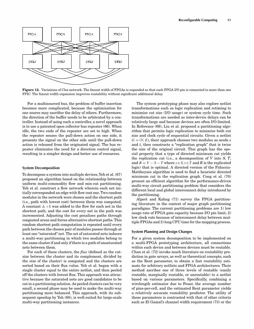
In practice, the first-level crossbar of the Clos networkis replaced with FPGAs to save board space (Fig. 11).Routability is worse than an ideal Clos network. Even witha true Clos network, complete routability of multipin netsis not guaranteed, which is an important practical consid-eration because in microelectronic design, many multipinnets typically exist.
In an attempt to solve the multipin net and routabilityproblem, we can introduce extra connections among FPIDsas shown in Fig. 12. However, extra FPID interconnectionsalso incur extra delay. We can also expand the fanout widthof FPGAs so that each FPGA I/O pin is connected to morethan one FPIC (60, 61). The fanout width expansion im-proves routability without significant additional delay. Themultiple appearances of I/O pins increase the probabilitythat a signal connection can be made in a single stage,which is especially critical for multipin nets. However, theadditional fanouts increase the needed pin count of FPICs.Thus, we need to find a balanced fanout distribution thatreduces the interconnect delay with a minimal pin require-ment.
A tree-structured network can simplify the mappingprocess for certain applications. In Reference (62), an ex-ample of a tree-structured network is illustrated for a VeryLarge Scale Simulator (VLSS). The VLSS tree structurehas all logic components located at the leaves and intercon-nect switches at the internal nodes. The machine covers acapacity of eight million gates. Each branch is an 8-bit bus.The higher up the level of the tree, the less parallelism thesignal distribution can achieve. Therefore, a partitioningprocess is designed to minimize the high level interconnectand maximize the parallel operation.
Interconnect Multiplexing
Time multiplexing is an effective method for tackling thescalability problem in interconnecting large designs. Thetime-sharing method can be extended from traditional busorganization (27, 62) to network sharing (63) and furtherto function block sharing (40).
Interconnect can be time shared as a bus (27, 62). If ncommunication lines exist between two FPGAs, they canbe reduced to a single line by storing logical outputs inshift registers and time-multiplexing the communication
in phases. Such a scheme was employed in the virtual wireslogic emulation system (27), which is efficient because in-terconnects are normally capable of being clocked at muchhigher rates than the critical path of the rest of the system,and all logical wires are not simultaneously active. Thisscheme can greatly reduce the complexity of the intercon-necting network or printed circuit board in a multi-FPGAsystem.
Li and Cheng (63) proposed that a dynamic network beviewed as overlapping L conventional FPICs together butsharing the same I/O pins. A dynamic routing architec-ture can increase the routability and shorten interconnectlength. Each switching network is a full crossbar,which canbe reconfigured to provide any connections among I/O pins.The select lines are used to activate only one switching net-work at a time; thus the I/O pins are dynamically connectedaccording to the configuration of this active switching net-work. By dynamically reconfiguring the FPICs, L logic sig-nals can time-share the same interconnect resources.
Memory Allocation
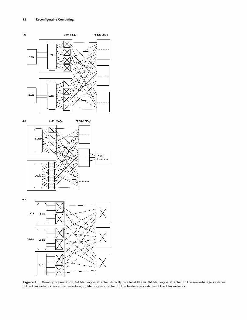
Interconnect schemes should also consider how memoryis connected to the FPGAs. Although combining memorywith logic in the same FPGA is the most desirable methodfor reducing routing congestion and signal delay, separatecomponents can supply much larger capacity at higher den-sity and lower price. Figure 13 demonstrates three differ-ent ways of allocating the memories in a Clos network (31,64). The memory may be attached directly to a local FPGA(Fig. 13a), attached to the second-stage switches of the Closnetwork via a host interface (Fig. 13b), or attached to thefirst-stage switches of the Clos network (Fig. 13c). The firstmethod provides good performance for local memory ac-cess. However, for the case of nonlocal memory access, theroutability and delay are concerns. The second method isslower than the first method for local memory accesses butprovides better routability. The third is the most flexible asthe memory is attached to the network and the routabil-ity is high. However, every logic-to-memory communicationmust go through the second interconnect stage.
Bus Buffer Insertion
In FPGAs, signal propagation is inherently slow because ofits programmable interconnect feature. However, the delayof long routing wires can be drastically reduced by bufferinsertion. The principle at work is that by inserting bufferswe can decouple capacitive effects of components and in-terconnect driven by the buffers and thereby improve RCdelay.
Given a routing topology for a net and timing require-ments for its sinks, an efficient optimal buffer insertionalgorithm was proposed in Reference 65. Experimental re-sults show dramatic improvement versus the unbufferedsolution. Thus, it is advantageous to have abundant buffersin FPGAs. However, each possible buffer and its pro-grammable switch adds capacitance to the wires, which inturn will contribute to delay. Thus, a balance point needs tobe identified to trade off between the additional delay andcapacitance of the buffers versus the improvement theycan provide.
10 Reconfigurable Computing
Figure 10. Folded Clos network. The three-stage Clos network is folded into a two-stage network so that the inputs and outputs aremixed in the first stage.
Figure 11. Variations of the Clos network. The first level crossbar of the Clos network is replaced with FPGAs to save board space.Routability is worse than an ideal Clos network.
Reconfigurable Computing 11
Figure 12. Variations of Clos network. The fanout width of FPGAs is expanded so that each FPGA I/O pin is connected to more than oneFPIC. The fanout width expansion improves routability without significant additional delay.
For a multisourced bus, the problem of buffer insertionbecomes more complicated, because the optimization forone source may sacrifice the delay of others. Furthermore,the direction of the buffer needs to be arbitrated by a con-troller. Instead of using such a controller, a novel approachis to use a patented open collector bus repeater (66). Whenidle, the two ends of the repeater are set to high. Whenthe repeater senses the pull-down action on one side, itpresents the signal on the other side until the pull-downaction is released from the originated signal. The bus re-peater eliminates the need for a direction control signal,resulting in a simpler design and better use of resources.
System Decomposition
To decompose a system into multiple devices,Yeh et al. (67)proposed an algorithm based on the relationship betweenuniform multi-commodity flow and min-cut partitioning.Yeh et al. construct a flow network wherein each net ini-tially corresponded an edge with flow cost one. Two randommodules in the network were chosen and the shortest path(i.e., path with lowest cost) between them was computed.A constant � <1 was added to the flow for each net in theshortest path, and the cost for every net in the path wasincremented. Adjusting the cost penalizes paths throughcongested areas and forces alternative shortest paths. Thisrandom shortest path computation is repeated until everypath between the chosen pair of modules passes through atleast one “saturated” net. The set of saturated nets inducesa multi-way partitioning in which two modules belong tothe same cluster if and only if there is a path of unsaturatednets between them.
For each of these clusters, the flux (defined as the cut-size between the cluster and its complement, divided bythe size of the cluster) is computed and the clusters aresorted based on their flux value. Yeh et al. began with asingle cluster equal to the entire netlist, and then peeledoff the clusters with lowest flux. This approach was attrac-tive because the saturated nets are good candidates to becut in a partitioning solution. As peeled clusters can be verysmall, a second phase may be used to make the multi-waypartitioning more balanced. This approach, with its sub-sequent speedup by Yeh (68), is well-suited for large-scalemulti-way partitioning instances.
The system prototyping phase may also explore netlisttransformations such as logic replication and retiming tominimize cut size (I/O usage) or system cycle time. Suchtransformations are needed as inter-device delays can berelatively large and because devices are often I/O-limited.In Reference (69), Liu et al. proposed a partitioning algo-rithm that permits logic replication to minimize both cutsize and clock cycle of sequential circuits. Given a netlistG = (V, E), their approach chooses two modules as seeds sand t, then constructs a “replication graph” that is twicethe size of the original circuit. This graph has the spe-cial property that a type of directed minimum cut yieldsthe replication cut (i.e., a decomposition of V into S, T,and R = V − S − T where s ∈ S, t ∈ T and R is the replicatedlogic) that is optimal. A directed version of the Fiduccia-Mattheyses algorithm is used to find a heuristic directedminimum cut in the replication graph. Cong et al. (70)present an efficient algorithm for the performance-drivenmulti-way circuit partitioning problem that considers thedifferent local and global interconnect delay introduced bythe partitioning.
Alpert and Kahng (71) survey the FPGA partition-ing literature in the context of major graph partitioningparadigms. The current partitioning problems are 1) lowusage rate of FPGA gate capacity because I/O pin limit, 2)low clock rate because of interconnect delay between mul-tiple FPGAs and 3) long CPU time for the mapping process.
System Planning and Design Changes
For a given system decomposition to be implemented ona multi-FPGA prototyping architecture, all connectionswithin each device and between devices must be routable.Chan et al. (72) invoke much literature on routability pre-diction in gate arrays, as well as theoretical concepts, suchas the Rent parameter, to obtain a fast routability esti-mate for arbitrary netlists and FPGA architectures. Theirmethod ascribes one of three levels of routable (easilyroutable, marginally routable, or unroutable) to a netlistbased on various parameters. Specifically, combining awirelength estimator due to Feuer, the average numberof pins-per-cell, and the estimated Rent parameter yieldsa relatively accurate routability predictor. The utility ofthese parameters is contrasted with that of other criteriasuch as El Gamal’s channel width requirement (73) or the
12 Reconfigurable Computing
Figure 13. Memory organization, (a) Memory is attached directly to a local FPGA. (b) Memory is attached to the second-stage switchesof the Clos network via a host interface, (c) Memory is attached to the first-stage switches of the Clos network.
Reconfigurable Computing 13
average pins-per-net ratio.In addition to routability, connections must also
meet system timing constraints. Selvidge et al. (74) ex-tend the original virtual wires (27) concept in theirTIERS (Topology-IndEpendent Routing and Scheduling)approach. The problem formulation assumes that an as-signment from a multiple-FPGA partitioning (i.e., a designgraph) to a target topology graph has already been made.The objective is to assign “links” (i.e., signal nets) to chan-nels between devices; as with the Virtual Wires concept,specific timeslices for a channel can be assigned to multi-ple links as long as no two links need to transmit signals atthe same time. The TIERS algorithm uses a greedy methodto order the links and then routes each link in the sched-uled order while reserving channel resources; factors of upto 2.5 improvement in system cycle time are achieved.
Chang, et al. (75) address the combined issues ofroutability and system timing by applying layout-drivenlogic resynthesis techniques. For a given wire that cannotbe routed, “alternative wires” and alternative functions areidentified, such that the given unroutable wire can be re-moved from the circuit and replaced with a new wire (orwires) or new logic without affecting functionality. Chenget al. estimate that between 30% and 50% of wires have so-called “triple-wire alternatives” (i.e., replacements consist-ing of three or fewer wires). Their method first routes thewires that do not have any alternatives then replaces anyunroutable wire with available alternatives. System tim-ing can be improved by replacing long wires with shorteralternatives.
CONCLUSION
Reconfigurable computing offers a middle ground betweensoftware-based systems and ASIC implementations, andis often able to combine important benefits of both. Im-plementations are able to avoid overheads such as unnec-essary data transfers, decoding and control mandatory inmicroprocessors, and designs can be optimized on a basisspecific to an application, a problem instance or even anexecution. Using this technology, it is possible to achievesize, performance, cost, or power improvements over moreconventional computing technologies.
ACKNOWLEDGMENTS
The authors would like to thank Y M. Lam for his help inpreparing this manuscript and Prof. Wayne Luk (ImperialCollege) for his proofreading of this article.
BIBLIOGRAPHY
1. Estrin, G. Reconfigurable Computer Origins: The UCLAFixed-plus-variable (F+V) Structure computer. IEEE Ann.Hist. Comput. 2002, 24 (4), pp 3–9.
2. Compton, K.; Hauck, S. The roles of FPGAs in Repro-grammable Systems. Proc. IEEE 1998, 86, (4), pp 615–639.
3. Bondalapati, K.; Prasanna, V. Reconfigurable Computing Sys-tem. Proc. IEEE 2002, 90 (7), pp 1201–1217.
4. Compton, K.; Hauck, S. Reconfigurable Computing: A Surveyof System and Software. ACM Comput.Surv. 2002, 34 (2), pp171–210.
5. Todman, T.; Constantinides, G.; Wilton, S.; Mencer, O.; Luk,W.; Cheung, P. Reconfigurable Computing: architectures anddesign methods. IEE Proc. Comput. Digit. Tech. 2000, 152, (2),pp 193–205.
6. DeHon,A. The Density Advantage of Configurable Computing.IEEE. Computer 2000, 33 (4), pp 41–49.
7. Tsoi, K. H.; Lee, K. H.; Leong, P.H.W. A Massively Parallel RC4Key Search Engine; Proc. of the 10th Annual IEEE Symposiumon Field-Programmable Custom Computing Machines FCCM;Washington, DC, IEEE Computer Society, 2002, pp 13–21.
8. Liang, J.; Tessier, R.; Goecket, D. A Dynamically-reconfigurable, Power-efficient Turbo Decoder; 2004, pp91–100.
9. Betz, V.; Rose, J.; Marquardt, A. Eds. Architecture and CADfor Deep-Submicron FPGAs; Kluwer Academic Publisher: Dor-drecht, the Netherlands, 1999.
10. Xilinx.http://www.xilinx.com (accessed 2006).11. Altera.http://www.altera.com (accessed 2006).12. Actel.http://www.actel.com (accessed 2006).13. Ahmed, E.; Rose, J. The Effect of LUT and Cluster Size on
Deep-submicron FPGA Performance and Density Proc. of the2000 ACM/SIGDA Eighth International Symposium on FieldProgrammable Gate Arrays ACM Press: New York, 2000; pp3–12.
14. Goldstein, S. C.; Schmit, H.; Budiu, M.; Cadambi, S.; Moe, M.;Taylor, R. R. Piperench: A Reconfigurable Architecture andCompiler. Computer 2000, 33 (4), pp 70–77.
15. Ebeling, C.; Cronquist, D. C.; Franklin, P. Rapid - Recon-figurable Pipelined Datapath; Proc. of the 6th InternationalWorkshop on Field-Programmable Logic, Smart Applications,New Paradigms and Compilers; London, UK, Springer-Verlag:l996, pp 126–135.
16. M2000. FPC06: http://www.m2000.fr (accessed 2006).17. eASIC. http://www.easic.com (accessed 2006).18. Wilton, S.; Kafafi, N.; Wu, J.; Bozman, K.; Aken’Oven, V.; Saleh,
R. Design Considerations for Soft Embedded ProgrammableLogic Core. IEEE Solid Circuits 2005, 40 (2), pp 485–497
19. Moll, L.; Vuillemn, J.; Boucard, P.; High-energy Physics onDECPeRLe-1 Programmable Active Memory; Proc. of the 1995ACM Third International Symposium on Field-programmableGate Arrays; New York, (FPGA 95), ACM Press: 1995, pp47–52.
20. Hoang, D. T. Searching Genetic Database on Splash, IEEEWorkshop on FPGAs for Custom Computing Machines, Napa,CA, April 1993, pp 185–191.
21. Ting, L.-K.;Woods, R.; Cowan, C. F. N. Virtex FPGA Implemen-tation of a Pipelined Adaptive LMS Predictor for ElectronicSupport Measure Receivers. IEEE Trans. VLSI Syst. 2005, 13(1), pp 86–95.
22. Chang, C.; Wawrzynek, J.; Brodersen, R. W. BEE2: A high-endReconfigurable Computing System. IEEE Des. Test 22 (2), pp114–125.
23. Shand, M.; Vuillemin, J.; Fast Implementations of RSA Cryp-tography: Proc. 11th Symposium on Computer Arithmetic,1993, pp 252–259.
24. Zhang, G. L.; Leong, P. H. W.; Ho, C. H.; Tsoi, K. H.; Cheung,C. C. C.; Lee, D. -U.; Cheung, R. C. C.; Luk, W. Reconfigurable
14 Reconfigurable Computing
Acceleration for Monte Carlo based financial simulation: Proc.International Conference on Field Programmable Technology(ICFPT). 2005, pp 215–222.
25. Vuillemin, J.; Patrice, B.; Didier, R.; Shand, M.; Herve, T.;Philippe, B. Programmable Active Memories: ReconfigurableSystem Come of Age. IEEE Trans. VLSI Syst. 1996, 4 (1), pp56–59.
26. Butts, M.; Batcheller, J.; Varghese, J.; An Efficient Logic Em-ulation System. IEEE Trans. Very Large Scale Integr. (VLSI)Syst. 1993, pp 171–173.
27. Babb, J.; Tessier, R.; Dahl, M.; Hanono, S. Z.; Hoki, D. M.;Agarwal, A. Logic Emulation with Virtual Wires. IEEE Trans.Computer-Aided Design 1997, 16 (6), p 609.
28. de Souza, L.; Ryan, P.; Crawford, J.; Wong, K.; Zyner, G.; Mc-Dermott, T. Prototyping for the Concurrent Development ofan IEEE 802.11 Wireless LAN Chaipset: Proc. InternationalConference on Field-Programmable Logic and its ApplicationsLNCS 2778, Springer, 2003, pp 51–60.
29. Cadence. http://www.cadence.com/datasheets/lncisivePalladiumllds.pdf (accessed 2006). Palladium DataSheet, 2005, pp 1–8.
30. Bertin, P.; Roncin, D.; Vuillemin, J. Introduction to Pro-grammable Active Memories. DEC Memo 3 1989, pp 1–9.
31. Chan, P. K.; Schlag, M. D. F. Architectural Tradeoffs in Field-programmable Devices Based Computing System; EEE Work-shop on FPGAs for Custom Computing Machines; l993, pp152–161
32. Mohsen, A. Programmable Interconnects Speed System Ver-ification. IEEE Circuits Devices Mag, 1993, 9 (3), pp 37–42.
33. Slimane-Kadi, M.; Brasen, D.; Saucier, G. A Fast-FPGA Pro-totyping System That Uses Inexpensive High-performanceFPIC. ACM Int. Workshop on FPGAs, Berkeley, CA, 1994, pp1.3. 1–11.
34. Arnold, J. M.; Buell, D. A.; Davis, E. G. SPLASH 2; 4th An-nual ACM Symposium on Parallel Algorithms and Architec-tures (SPAA 9Z); 1992, pp 316–322.
35. Cray. http://www.cray.com/downloads/Cray XDl Datasheet.pdf(accessed 2006). Cray XDl Datasheet.
36. SRC Computers. http://www.srccomp.com (accessed 2006).37. SGI. http://www.sgi.com/products/rasc/ (accessed 2006).38. Villasenor, J.; Mangione-Smith, W. H. Configurable Comput-
ing. Scientif. Amer. 1997, pp 67–71.39. Becker, J.; Hubner, M. Run-time Reconfigurability and Other
Future Trendy; Proc. of the 19th Annual Symposium on Inte-grated Circuits and Systems Design (SBCCI 06); ACM Press:New York, 2006, pp 9–11.
40. Bhat, N. B.; Chaudhary, K.; Kuh, E. S. Performance-oriented Fully Routable Dynamic Architecture for a Field-programmable Logic Device. Memorandum No. UCB/ERLM93/42, Electronics Research Lab., College of Engineering,UC Berkeley, 1993, pp. 1–21.
41. NEC Electronics. http://www.necel.com/drp/in/index.html (ac-cessed 2006).
42. Wirthlin, M. J.; Hutchings, B. L. A Dynamic Instruction SetComputing; Proc. of the IEEE Symposium on FPGA’s for Com-puting Machines Washington, DC, IEEE Computer Society,1995, pp 99–107.
43. Stretch, Inc. http://www.stretchinc.com (accessed 2006).44. Steiger, C.; Walder, H.; Platzner, M. Operting System for Re-
configurable Embedded Platforms: Online Scheduling of Real-time Task. IEEE Trans. Comput. 2004, 53 (11), pp 1393–1407.
45. Schmit, H. Incremental Reconfiguration for Pipelined Applica-tions; Proc. of the 5th IEEE Symposium on FPGA-Based Cus-tom Computing Machines Washington, DC, IEEE ComputerSociety, 1997, pp 47–55.
46. Young, S.; Alfke, P.; Fewer, C.; McMillan, S.; Blodget, B.; Levi,D. A High I/O Reconfigurable Crossbar Switch; Proc. of the11th Annual IEEE Symposium on Field-Programmable Cus-tom Computing Machines (FCCM 03); Washington, DC, IEEEComputer Society, 2003, pp 3–10.
47. Guccione, S.; Levi, D.; Sundarajan, P. A Java-based Inter-face for Reconfigurable Computing; Second Annual Mili-tary and Aerospace Applications of Programmable Devicesand Technologies Conference (MAPLD); September 1999. cite-seer.ist.psu.edu/681383.html.
48. Luk,W.; Page, I. Compiling Occam into FPGAs. FPGAs. Abing-don, EE &CS books: 1991; pp 271–283.
49. Page, I. Constructing Hardware/Software System From a Sin-gle Description. VLSI Signal Processing, 1996, 12,pp 87–107.
50. Celoxica. http://www.celoxica.com (accessed 2006).51. Mentor Graphics. http://www.mentor.com/products/esl/high
level synthesis/catapult synthesis/index.cfm (accessed2006).
52. Mathworks, Inc. http://www.mathworks.com (accessed 2006).53. Haldar, M.; Nayak, A.; Choudhary, A.; Banerjee, P. A System
for Synthesizing Optimized FPGA Hardware from MATLAB;Proc. of the 2001 IEEE/ACM International Conference onComputer-aided Design (ICCAD) Piscataway, NJ, IEEE Press:2001, pp 314–319.
54. Lau, D.; Pritchard, O.; Molson, P. Automated Generationof Hardware Accelerators with Direct Memory Access fromANSI/ISO Standard C Functions, Proc. of the 14th AnnualIEEE symposium on Field-Programmable Custom ComputingMachines (FCCM’06), Washington, DC, IEEE Computer Soci-ety, 2006, pp 45–56.
55. Isshiki,T.; Dai,W. M. High-level Bit-serial Datapath Synthesisfor Multi-FPGA System; International Workshop on FPGAs;1995, pp 167–174.
56. Leong, M. P.; Leong, P. H. W. A Variable-Radix Digit-serialDesign Methodology and Application to the Discrete CosineTransform. IEEE Trans. VLSI System 2003, 11 (1), pp 90–104.
57. Clos, C. A Study of Nonblocking Switching Networks. Bell Sys-tem Tech. J. 1953, 32,pp 406–424.
58. Benes, V.E. Mathematical Theory of Connecting Networks andTelephone Traffic; Academic Press: New York, 1965.
59. Cole, R.; Hopcroft, J. On Edge Coloring Bipartite Graphs.SIAM J.Computing 1982, 11,pp 540–546.
60. Richards, G. W.; Hwang, F. K.A Two-stage RearrangeableBroadcast Switching Network. IEEE Trans. Commun. 1985,COM- 33(10), pp 1025–1035.
61. I-Cube, Using FPID Devies in FPGA-based Prototyping. Ap-plication Note 1994, pp 1–11.
62. Wei, Y. C.; Cheng, C. K.; Wurman, Z. Multiple-level Partition-ing: An Application to the Very Large-Scale HardWare Simu-lator. IEEE J. Solid State Circuits 1991, pp 706–716.
63. Li, J.; Cheng, C. K.. Routability Improvement Using DynamicInterconnect Architecture. IEEE FPGAs for Custom Comput-ing Machines 1995, Apr, pp 13.2.–7.
64. Chan, P. K.; Schlag, M. D. F.; Martin, M. BORG: A Reconfig-urable Prototyping Board Using Field-programmable Gate Ar-rays. Int. Workshop on FPGA; Berkeley CA, 1992, pp 47–51.
Reconfigurable Computing 15
65. Lillis, J.; Cheng, C. K.;Lin,T.T. OptimalWire Sizing and BufferInsertion for Low Power and a Generalized Delay Model.IEEE/ACM Int. Conf. on Computer-Aided Design; 1995, pp138–143.
66. Hsieh,W. J.; Jenq,Y. C.; Horng, C. S.; Lofstrom, K. Input/outputI/O Bidirectional Buffer for Interfacing I/O Parts of a FieldProgrammable Interconnection Device with Array Ports of aCross-point Switch. US Patent no 5,428,800, 1992, pp 1–13.
67. Yeh, C. W.; Cheng, C. K.; Lin, T.T. A ProbabilisticMulticommodity-flow Solution to Circuit Clustering Prob-lems. IEEE Int. Conf. on Computer-Aided Design; 1992, pp428–431.
68. Yeh, C. W. On the Acceleration of Flow-oriented Circuit Clus-tering. IEEE Trans. Comput.-Aided Des. Integr. Circuits Syst.1995, pp 1305–1308.
69. Liu, L. T.; Kuo, M. T.; Cheng, C. K.; Hu, T.C. Performance-driven Partitioning Using a Replication Graph Approach.ACM/IEEE Design Automation Conf; June 1995, pp 206–210.
70. Cong, J.; Lim, S. K.; Wu, C. Performance driven Multi-leveland Multiway Partitioning with Retiming; Proc. of the 37thConference on Design Automation (DAC 00); New York, ACMpress: 2000, pp 274–279.
71. Alpert, C. J.; Kahng, A.B. Recent Directions in Netlist Par-titioning: A Survey. Integration, The VLSI. 1995, August,pp1–81.
72. Chan, P. K.; Schlag, M. D. F.; Zien, J. Y. On routability Predic-tion for Field-programmable Gate Arrays; IEEE Design Au-tomation Conf.; Dallas, 1993, pp 326–330.
73. El Gamal, A. Two-dimensional Stochastic Model for Inter-connections in Master Slice Integrated Circuits. IEEE Trans.CAS. 1981, 28 (2), pp 127–138.
74. Selvide, C.; Agarwal, A.; Dahl, M.; Babb, J. TIERS: TopologyIndependent Pipelined Routing and Scheduling; Int. Symp. onFPGA; 1995, pp 25–31.
75. Chang, S. C.; Cheng, K. T.; Woo, N. S.; Marek-Sadowska, M.Layout Driven Logic Synthesis for FPGA; Proc. ACM/IEEEDesign Automation Conference. 1994, pp 308–313.
76. Leong, M. P. FPGA Design Methodologies for High Perfor-mance Applications. PhD dissertation, The Chinese Univer-sity of Hong Kong, 2001.
CHENG CHUNG-KUAN
ANDREW B. KAHNG
PHILIP H.W. LEONG
Dept. of Computer Science andEngineering, University ofCalifornia, La Jolla,California
Dept. of Computer Science andEngineering, The ChineseUniversity of Hong Kong,Shatin, Hong Kong