Embed Size (px)
Citation preview
VS1000
VS1000 - Ogg Vorbis Player IC withUSB and NAND FLASH Interface
Hardware Features• Low-power operation• Single input voltage: Internal voltage reg-
ulation for analog, digital, and I/O power• Operates with a single 12 MHz clock• Internal PLL clock multiplier• Power button pin,
software-controlled power-off• USB Full Speed hardware• NAND FLASH interface with ECC• I/O for user interface• High-quality on-chip stereo DAC with no
phase error between channels• Stereo earphone driver capable of
driving a 30 Ω load• Lead-free RoHS-compliant package
(Green)
Firmware Features• Implements USB Mass Storage Device
and Audio Device• NAND FLASH handling with error cor-
rection, block remapping, and wear lev-elling
• Default player application in firmware– Decodes Ogg Vorbis, sound level
normalization using Replay Gain– Pause / Play– Volume control– Next / Previous Song– Rewind and Fast Forward– Random Play– EarSpeaker Spatial Processing
• Bass and treble controls for customizedplayer
• NAND FLASH boot for customized player• SPI FLASH boot for special applications• UART for debugging and special appli-
cations
DescriptionVS1000 is a single-chip Ogg Vorbis (license-free audio codec) player and a system-on-a-chip (SoC) for various control and audio ap-plications. VS1000 contains a high-perfor-mance low-power DSP core VSDSP4, NANDFLASH interface, Full Speed USB port, gen-eral purpose I/O pins, SPI, UART, as well as ahigh-quality variable-sample-rate stereo DAC,and an earphone amplifier and a commonvoltage buffer.
VS1000 firmware implements a default playerthat reads and plays files from NAND FLASH.The player can be customized or replaced byboot from NAND FLASH or SPI memory.
When connected to USB, the firmware imple-ments USB Mass Storage Device protocol oracts as an Audio Device, providing a single-chip USB headphone application.
EarSpeaker spatial processing provides morenatural sound in headphone listening condi-tions. It widens the stereo image and posi-tions the sound sources outside the listener’shead.
SPI EEPROM can be used to load code inapplications that do not use NAND FLASH.
Version: 1.43, 2013-05-28 1
VS1000CONTENTS
Contents
VS1000 1
Table of Contents 2
List of Figures 3
1 Disclaimer 4
2 Definitions 4
3 Characteristics & Specifications 53.1 Absolute Maximum Ratings . . . . . . . . . . . . . . . . . . . . . . . . . . . . . 53.2 Recommended Operating Conditions . . . . . . . . . . . . . . . . . . . . . . . . 53.3 Analog Characteristics of Audio Outputs . . . . . . . . . . . . . . . . . . . . . . 63.4 Analog Characteristics of Regulators . . . . . . . . . . . . . . . . . . . . . . . . 73.5 Analog Characteristics of VHIGH Voltage Monitor . . . . . . . . . . . . . . . . . 83.6 Analog Characteristics of CVDD Voltage Monitor . . . . . . . . . . . . . . . . . 83.7 Power Button Characteristics . . . . . . . . . . . . . . . . . . . . . . . . . . . . 83.8 Analog Characteristics of USB . . . . . . . . . . . . . . . . . . . . . . . . . . . . 83.9 Power Consumption . . . . . . . . . . . . . . . . . . . . . . . . . . . . . . . . . 93.10 Digital Characteristics . . . . . . . . . . . . . . . . . . . . . . . . . . . . . . . . . 9
4 Packages and Pin Descriptions 104.1 Packages . . . . . . . . . . . . . . . . . . . . . . . . . . . . . . . . . . . . . . . 104.2 LQFP-48 Pin Descriptions . . . . . . . . . . . . . . . . . . . . . . . . . . . . . . 11
5 Example Schematic 13
6 VS1000 Functional Blocks 146.1 Regulator Section . . . . . . . . . . . . . . . . . . . . . . . . . . . . . . . . . . . 146.2 Digital Section . . . . . . . . . . . . . . . . . . . . . . . . . . . . . . . . . . . . . 156.3 Analog Section . . . . . . . . . . . . . . . . . . . . . . . . . . . . . . . . . . . . 17
7 Firmware Operation 187.1 SPI Boot . . . . . . . . . . . . . . . . . . . . . . . . . . . . . . . . . . . . . . . . 187.2 NAND FLASH Probe . . . . . . . . . . . . . . . . . . . . . . . . . . . . . . . . . 197.3 UART Boot/Monitor . . . . . . . . . . . . . . . . . . . . . . . . . . . . . . . . . . 207.4 Default Firmware Features . . . . . . . . . . . . . . . . . . . . . . . . . . . . . . 21
7.4.1 USB Mass Storage and Audio Device . . . . . . . . . . . . . . . . . . 217.4.2 Default Player Application . . . . . . . . . . . . . . . . . . . . . . . . 21
7.5 Supported Audio Codecs . . . . . . . . . . . . . . . . . . . . . . . . . . . . . . . 237.5.1 Supported Ogg Vorbis Formats . . . . . . . . . . . . . . . . . . . . . 237.5.2 Additional Formats . . . . . . . . . . . . . . . . . . . . . . . . . . . . 23
7.6 EarSpeaker Spatial Processing . . . . . . . . . . . . . . . . . . . . . . . . . . . 24
8 VS1000 Errata 25
9 Document Version Changes 26
10 Contact Information 27
Version: 1.43, 2013-05-28 2
VS1000LIST OF FIGURES
List of Figures
1 VS1000 pin configuration, LQFP-48. . . . . . . . . . . . . . . . . . . . . . . . . . 102 VS1000 pins, LQFP-48. . . . . . . . . . . . . . . . . . . . . . . . . . . . . . . . . 103 VS1000 example schematic. Use 100 kΩ for R25, R26, R17, R18, R10, R30,
R24, R12. Use 10 kΩ for R27, R28, R29, R31, R32, R19, R13. Populate onlyone of R12 and R13. . . . . . . . . . . . . . . . . . . . . . . . . . . . . . . . . . . 13
4 VS1000 block diagram. . . . . . . . . . . . . . . . . . . . . . . . . . . . . . . . . 145 EarSpeaker externalized sound sources vs. normal inside-the-head sound. . . . 24
Version: 1.43, 2013-05-28 3
VS10002 DEFINITIONS
1 Disclaimer
All properties and figures are subject to change.
2 Definitions
B Byte, 8 bits.
b Bit.
Ki “Kibi” = 210 = 1,024 (IEC 60027-2).
Mi “Mebi” = 220 = 1,048,576 (IEC 60027-2).
Gi “Gibi” = 230 = 1,073,741,824 (IEC 60027-2).
VS_DSP VLSI Solution’s DSP core.
W Word. In VS_DSP, instruction words are 32-bit and data words are 16-bit wide.
Version: 1.43, 2013-05-28 4
VS10003 CHARACTERISTICS & SPECIFICATIONS
3 Characteristics & Specifications
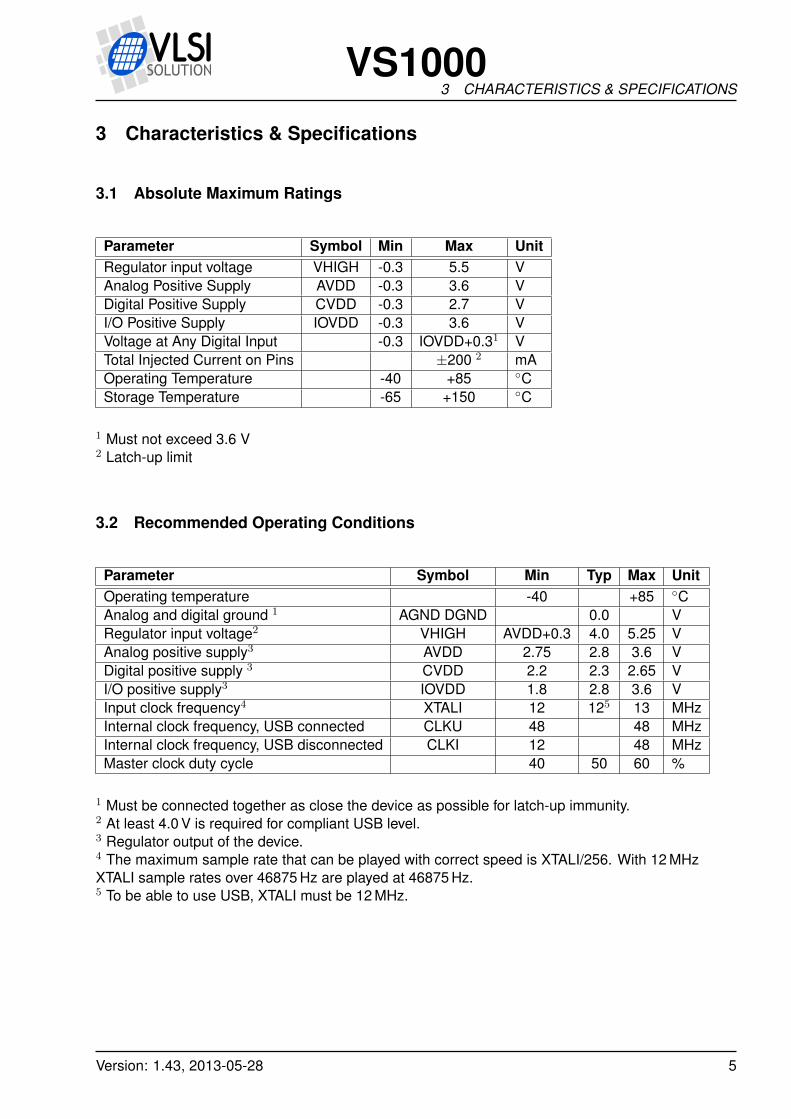
3.1 Absolute Maximum Ratings
Parameter Symbol Min Max UnitRegulator input voltage VHIGH -0.3 5.5 VAnalog Positive Supply AVDD -0.3 3.6 VDigital Positive Supply CVDD -0.3 2.7 VI/O Positive Supply IOVDD -0.3 3.6 VVoltage at Any Digital Input -0.3 IOVDD+0.31 VTotal Injected Current on Pins ±200 2 mAOperating Temperature -40 +85 CStorage Temperature -65 +150 C
1 Must not exceed 3.6 V2 Latch-up limit
3.2 Recommended Operating Conditions
Parameter Symbol Min Typ Max UnitOperating temperature -40 +85 CAnalog and digital ground 1 AGND DGND 0.0 VRegulator input voltage2 VHIGH AVDD+0.3 4.0 5.25 VAnalog positive supply3 AVDD 2.75 2.8 3.6 VDigital positive supply 3 CVDD 2.2 2.3 2.65 VI/O positive supply3 IOVDD 1.8 2.8 3.6 VInput clock frequency4 XTALI 12 125 13 MHzInternal clock frequency, USB connected CLKU 48 48 MHzInternal clock frequency, USB disconnected CLKI 12 48 MHzMaster clock duty cycle 40 50 60 %
1 Must be connected together as close the device as possible for latch-up immunity.2 At least 4.0 V is required for compliant USB level.3 Regulator output of the device.4 The maximum sample rate that can be played with correct speed is XTALI/256. With 12 MHzXTALI sample rates over 46875 Hz are played at 46875 Hz.5 To be able to use USB, XTALI must be 12 MHz.
Version: 1.43, 2013-05-28 5
VS10003 CHARACTERISTICS & SPECIFICATIONS
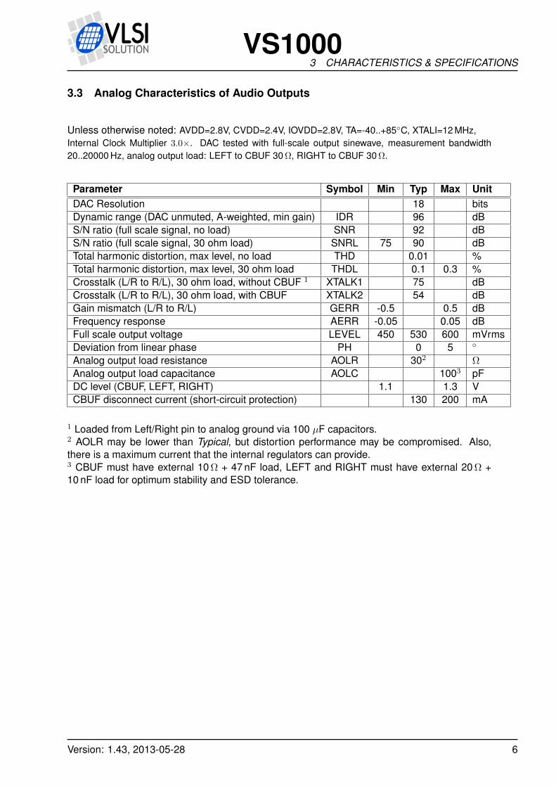
3.3 Analog Characteristics of Audio Outputs
Unless otherwise noted: AVDD=2.8V, CVDD=2.4V, IOVDD=2.8V, TA=-40..+85C, XTALI=12 MHz,Internal Clock Multiplier 3.0×. DAC tested with full-scale output sinewave, measurement bandwidth20..20000 Hz, analog output load: LEFT to CBUF 30 Ω, RIGHT to CBUF 30 Ω.
Parameter Symbol Min Typ Max UnitDAC Resolution 18 bitsDynamic range (DAC unmuted, A-weighted, min gain) IDR 96 dBS/N ratio (full scale signal, no load) SNR 92 dBS/N ratio (full scale signal, 30 ohm load) SNRL 75 90 dBTotal harmonic distortion, max level, no load THD 0.01 %Total harmonic distortion, max level, 30 ohm load THDL 0.1 0.3 %Crosstalk (L/R to R/L), 30 ohm load, without CBUF 1 XTALK1 75 dBCrosstalk (L/R to R/L), 30 ohm load, with CBUF XTALK2 54 dBGain mismatch (L/R to R/L) GERR -0.5 0.5 dBFrequency response AERR -0.05 0.05 dBFull scale output voltage LEVEL 450 530 600 mVrmsDeviation from linear phase PH 0 5
Analog output load resistance AOLR 302 Ω
Analog output load capacitance AOLC 1003 pFDC level (CBUF, LEFT, RIGHT) 1.1 1.3 VCBUF disconnect current (short-circuit protection) 130 200 mA
1 Loaded from Left/Right pin to analog ground via 100 µF capacitors.2 AOLR may be lower than Typical, but distortion performance may be compromised. Also,there is a maximum current that the internal regulators can provide.3 CBUF must have external 10 Ω + 47 nF load, LEFT and RIGHT must have external 20 Ω +10 nF load for optimum stability and ESD tolerance.
Version: 1.43, 2013-05-28 6
VS10003 CHARACTERISTICS & SPECIFICATIONS
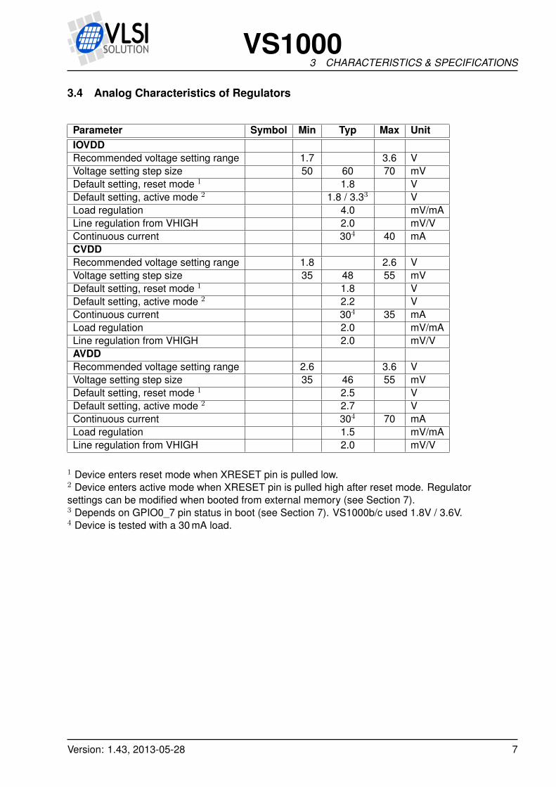
3.4 Analog Characteristics of Regulators
Parameter Symbol Min Typ Max UnitIOVDDRecommended voltage setting range 1.7 3.6 VVoltage setting step size 50 60 70 mVDefault setting, reset mode 1 1.8 VDefault setting, active mode 2 1.8 / 3.33 VLoad regulation 4.0 mV/mALine regulation from VHIGH 2.0 mV/VContinuous current 304 40 mACVDDRecommended voltage setting range 1.8 2.6 VVoltage setting step size 35 48 55 mVDefault setting, reset mode 1 1.8 VDefault setting, active mode 2 2.2 VContinuous current 304 35 mALoad regulation 2.0 mV/mALine regulation from VHIGH 2.0 mV/VAVDDRecommended voltage setting range 2.6 3.6 VVoltage setting step size 35 46 55 mVDefault setting, reset mode 1 2.5 VDefault setting, active mode 2 2.7 VContinuous current 304 70 mALoad regulation 1.5 mV/mALine regulation from VHIGH 2.0 mV/V
1 Device enters reset mode when XRESET pin is pulled low.2 Device enters active mode when XRESET pin is pulled high after reset mode. Regulatorsettings can be modified when booted from external memory (see Section 7).3 Depends on GPIO0_7 pin status in boot (see Section 7). VS1000b/c used 1.8V / 3.6V.4 Device is tested with a 30 mA load.
Version: 1.43, 2013-05-28 7
VS10003 CHARACTERISTICS & SPECIFICATIONS
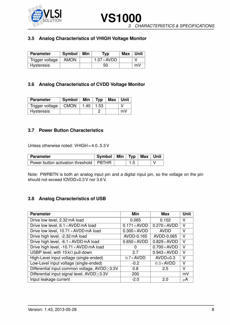
3.5 Analog Characteristics of VHIGH Voltage Monitor
Parameter Symbol Min Typ Max UnitTrigger voltage AMON 1.07×AVDD VHysteresis 50 mV
3.6 Analog Characteristics of CVDD Voltage Monitor
Parameter Symbol Min Typ Max UnitTrigger voltage CMON 1.40 1.53 VHysteresis 2 mV
3.7 Power Button Characteristics
Unless otherwise noted: VHIGH = 4.0..5.3 V
Parameter Symbol Min Typ Max UnitPower button activation threshold PBTHR 1.5 V
Note: PWRBTN is both an analog input pin and a digital input pin, so the voltage on the pinshould not exceed IOVDD+0.3 V nor 3.6 V.
3.8 Analog Characteristics of USB
Parameter Min Max UnitDrive low level, 2.32 mA load 0.065 0.102 VDrive low level, 6.1×AVDD mA load 0.171×AVDD 0.270×AVDD VDrive low level, 10.71×AVDD mA load 0.300×AVDD AVDD VDrive high level, -2.32 mA load AVDD-0.165 AVDD-0.065 VDrive high level, -6.1×AVDD mA load 0.650×AVDD 0.829×AVDD VDrive high level, -10.71×AVDD mA load 0 0.700×AVDD VUSBP level, with 15 kΩ pull-down 2.7 0.943×AVDD VHigh-Level input voltage (single-ended) 0.7×AVDD AVDD+0.3 VLow-Level input voltage (single-ended) -0.2 0.3×AVDD VDifferential input common voltage, AVDD≥3.3V 0.8 2.5 VDifferential input signal level, AVDD≥3.3V 200 mVInput leakage current -2.0 2.0 µA
Version: 1.43, 2013-05-28 8
VS10003 CHARACTERISTICS & SPECIFICATIONS
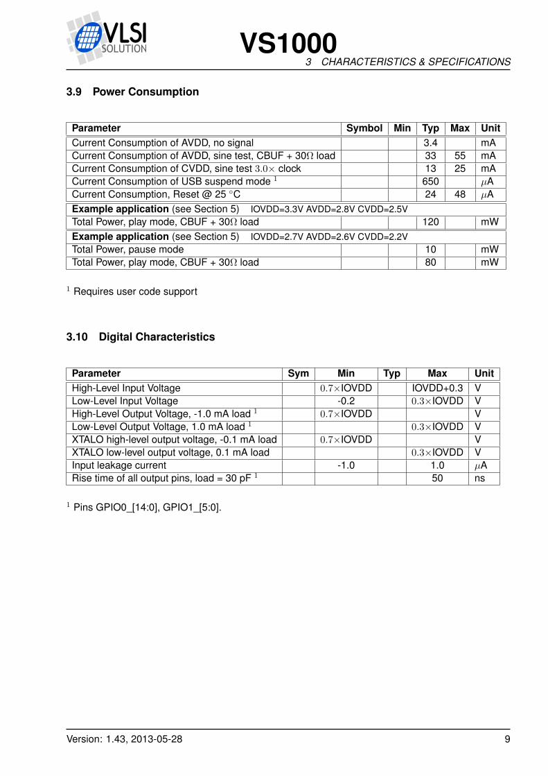
3.9 Power Consumption
Parameter Symbol Min Typ Max UnitCurrent Consumption of AVDD, no signal 3.4 mACurrent Consumption of AVDD, sine test, CBUF + 30Ω load 33 55 mACurrent Consumption of CVDD, sine test 3.0× clock 13 25 mACurrent Consumption of USB suspend mode 1 650 µACurrent Consumption, Reset @ 25 C 24 48 µAExample application (see Section 5) IOVDD=3.3V AVDD=2.8V CVDD=2.5VTotal Power, play mode, CBUF + 30Ω load 120 mWExample application (see Section 5) IOVDD=2.7V AVDD=2.6V CVDD=2.2VTotal Power, pause mode 10 mWTotal Power, play mode, CBUF + 30Ω load 80 mW
1 Requires user code support
3.10 Digital Characteristics
Parameter Sym Min Typ Max UnitHigh-Level Input Voltage 0.7×IOVDD IOVDD+0.3 VLow-Level Input Voltage -0.2 0.3×IOVDD VHigh-Level Output Voltage, -1.0 mA load 1 0.7×IOVDD VLow-Level Output Voltage, 1.0 mA load 1 0.3×IOVDD VXTALO high-level output voltage, -0.1 mA load 0.7×IOVDD VXTALO low-level output voltage, 0.1 mA load 0.3×IOVDD VInput leakage current -1.0 1.0 µARise time of all output pins, load = 30 pF 1 50 ns
1 Pins GPIO0_[14:0], GPIO1_[5:0].
Version: 1.43, 2013-05-28 9
VS10004 PACKAGES AND PIN DESCRIPTIONS
4 Packages and Pin Descriptions
4.1 Packages
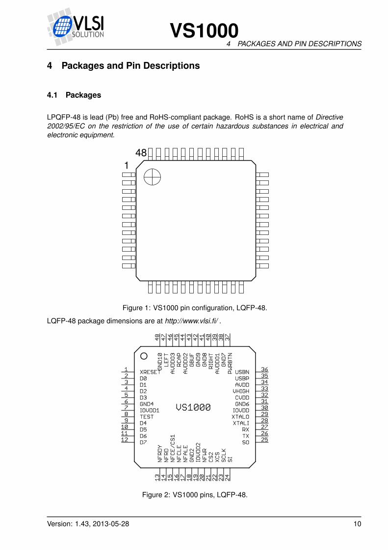
LPQFP-48 is lead (Pb) free and RoHS-compliant package. RoHS is a short name of Directive2002/95/EC on the restriction of the use of certain hazardous substances in electrical andelectronic equipment.
1
48
Figure 1: VS1000 pin configuration, LQFP-48.
LQFP-48 package dimensions are at http://www.vlsi.fi/ .
Figure 2: VS1000 pins, LQFP-48.
Version: 1.43, 2013-05-28 10
VS10004 PACKAGES AND PIN DESCRIPTIONS
4.2 LQFP-48 Pin Descriptions
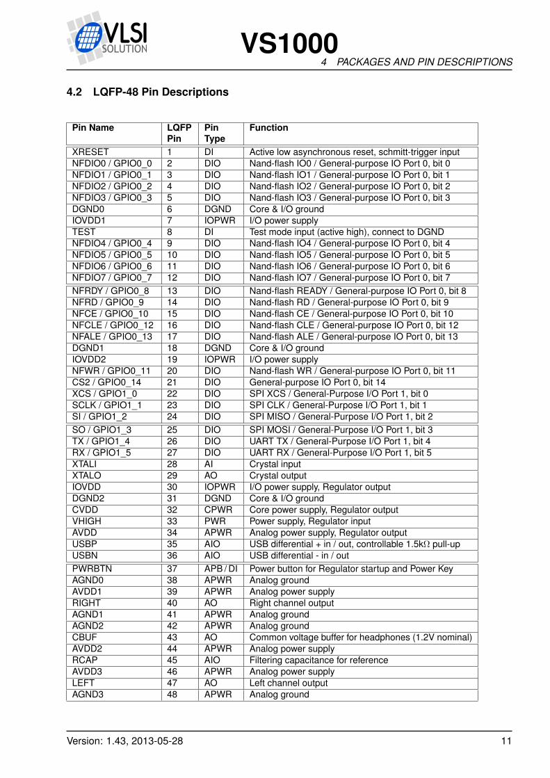
Pin Name LQFPPin
PinType
Function
XRESET 1 DI Active low asynchronous reset, schmitt-trigger inputNFDIO0 / GPIO0_0 2 DIO Nand-flash IO0 / General-purpose IO Port 0, bit 0NFDIO1 / GPIO0_1 3 DIO Nand-flash IO1 / General-purpose IO Port 0, bit 1NFDIO2 / GPIO0_2 4 DIO Nand-flash IO2 / General-purpose IO Port 0, bit 2NFDIO3 / GPIO0_3 5 DIO Nand-flash IO3 / General-purpose IO Port 0, bit 3DGND0 6 DGND Core & I/O groundIOVDD1 7 IOPWR I/O power supplyTEST 8 DI Test mode input (active high), connect to DGNDNFDIO4 / GPIO0_4 9 DIO Nand-flash IO4 / General-purpose IO Port 0, bit 4NFDIO5 / GPIO0_5 10 DIO Nand-flash IO5 / General-purpose IO Port 0, bit 5NFDIO6 / GPIO0_6 11 DIO Nand-flash IO6 / General-purpose IO Port 0, bit 6NFDIO7 / GPIO0_7 12 DIO Nand-flash IO7 / General-purpose IO Port 0, bit 7NFRDY / GPIO0_8 13 DIO Nand-flash READY / General-purpose IO Port 0, bit 8NFRD / GPIO0_9 14 DIO Nand-flash RD / General-purpose IO Port 0, bit 9NFCE / GPIO0_10 15 DIO Nand-flash CE / General-purpose IO Port 0, bit 10NFCLE / GPIO0_12 16 DIO Nand-flash CLE / General-purpose IO Port 0, bit 12NFALE / GPIO0_13 17 DIO Nand-flash ALE / General-purpose IO Port 0, bit 13DGND1 18 DGND Core & I/O groundIOVDD2 19 IOPWR I/O power supplyNFWR / GPIO0_11 20 DIO Nand-flash WR / General-purpose IO Port 0, bit 11CS2 / GPIO0_14 21 DIO General-purpose IO Port 0, bit 14XCS / GPIO1_0 22 DIO SPI XCS / General-Purpose I/O Port 1, bit 0SCLK / GPIO1_1 23 DIO SPI CLK / General-Purpose I/O Port 1, bit 1SI / GPIO1_2 24 DIO SPI MISO / General-Purpose I/O Port 1, bit 2SO / GPIO1_3 25 DIO SPI MOSI / General-Purpose I/O Port 1, bit 3TX / GPIO1_4 26 DIO UART TX / General-Purpose I/O Port 1, bit 4RX / GPIO1_5 27 DIO UART RX / General-Purpose I/O Port 1, bit 5XTALI 28 AI Crystal inputXTALO 29 AO Crystal outputIOVDD 30 IOPWR I/O power supply, Regulator outputDGND2 31 DGND Core & I/O groundCVDD 32 CPWR Core power supply, Regulator outputVHIGH 33 PWR Power supply, Regulator inputAVDD 34 APWR Analog power supply, Regulator outputUSBP 35 AIO USB differential + in / out, controllable 1.5kΩ pull-upUSBN 36 AIO USB differential - in / outPWRBTN 37 APB / DI Power button for Regulator startup and Power KeyAGND0 38 APWR Analog groundAVDD1 39 APWR Analog power supplyRIGHT 40 AO Right channel outputAGND1 41 APWR Analog groundAGND2 42 APWR Analog groundCBUF 43 AO Common voltage buffer for headphones (1.2V nominal)AVDD2 44 APWR Analog power supplyRCAP 45 AIO Filtering capacitance for referenceAVDD3 46 APWR Analog power supplyLEFT 47 AO Left channel outputAGND3 48 APWR Analog ground
Version: 1.43, 2013-05-28 11
VS10004 PACKAGES AND PIN DESCRIPTIONS
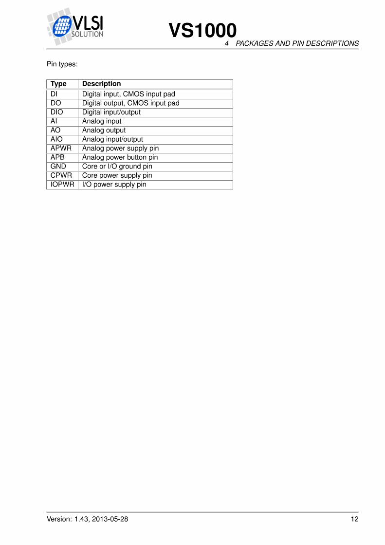
Pin types:
Type DescriptionDI Digital input, CMOS input padDO Digital output, CMOS input padDIO Digital input/outputAI Analog inputAO Analog outputAIO Analog input/outputAPWR Analog power supply pinAPB Analog power button pinGND Core or I/O ground pinCPWR Core power supply pinIOPWR I/O power supply pin
Version: 1.43, 2013-05-28 12
VS10005 EXAMPLE SCHEMATIC
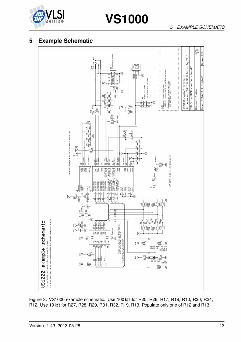
5 Example Schematic
Figure 3: VS1000 example schematic. Use 100 kΩ for R25, R26, R17, R18, R10, R30, R24,R12. Use 10 kΩ for R27, R28, R29, R31, R32, R19, R13. Populate only one of R12 and R13.
Version: 1.43, 2013-05-28 13
VS10006 VS1000 FUNCTIONAL BLOCKS
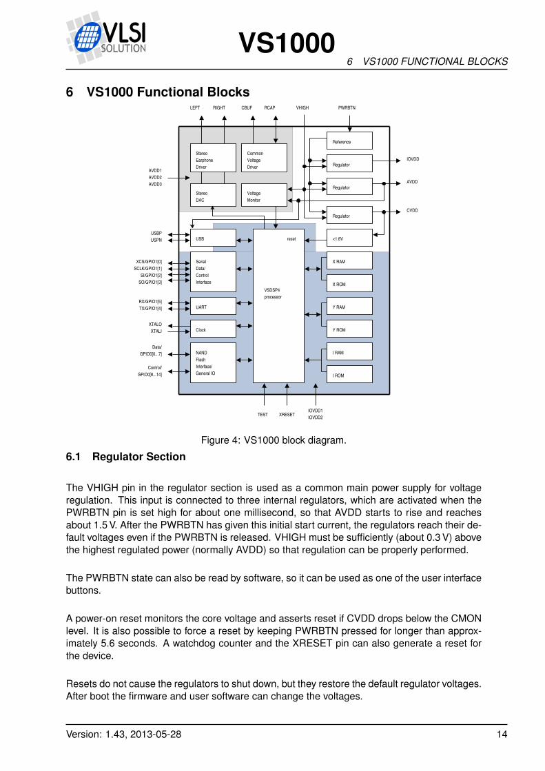
6 VS1000 Functional Blocks
Reference
Regulator
Regulator
Regulator
Common
Voltage
Driver
Voltage
Monitor
Stereo
Earphone
Driver
Stereo
DAC
AVDD1
AVDD2
AVDD3
Serial
Data/
Control
Interface
UART
Clock
NAND
Flash
Interface/
General IO
<1.6VUSB
X RAM
X ROM
Y RAM
Y ROM
I RAM
I ROM
VSDSP4
processor
USBP
USPN
XCS/GPIO1[0]
SCLK/GPIO1[1]
SI/GPIO1[2]
SO/GPIO1[3]
RX/GPIO1[5]
TX/GPIO1[4]
XTALO
XTALI
Data/
GPIO0[0...7]
Control/
GPIO0[8...14]
XRESETTEST
IOVDD
AVDD
CVDD
IOVDD1
IOVDD2
PWRBTNVHIGHRCAPCBUFRIGHTLEFT
reset
Figure 4: VS1000 block diagram.
6.1 Regulator Section
The VHIGH pin in the regulator section is used as a common main power supply for voltageregulation. This input is connected to three internal regulators, which are activated when thePWRBTN pin is set high for about one millisecond, so that AVDD starts to rise and reachesabout 1.5 V. After the PWRBTN has given this initial start current, the regulators reach their de-fault voltages even if the PWRBTN is released. VHIGH must be sufficiently (about 0.3 V) abovethe highest regulated power (normally AVDD) so that regulation can be properly performed.
The PWRBTN state can also be read by software, so it can be used as one of the user interfacebuttons.
A power-on reset monitors the core voltage and asserts reset if CVDD drops below the CMONlevel. It is also possible to force a reset by keeping PWRBTN pressed for longer than approx-imately 5.6 seconds. A watchdog counter and the XRESET pin can also generate a reset forthe device.
Resets do not cause the regulators to shut down, but they restore the default regulator voltages.After boot the firmware and user software can change the voltages.
Version: 1.43, 2013-05-28 14
VS10006 VS1000 FUNCTIONAL BLOCKS
Return to power-off is possible only with active software control (VSDSP writes the regulatorshutdown bit), or when VHIGH voltage is removed for a sufficiently long time. In the defaultfirmware player the power button has to be pressed for 2 seconds to make the software power-down the system and turn the regulators off.
6.2 Digital Section
Two of the regulators provide power supply for the digital section.
IOVDD is used for the level-shifters of the digital I/O and crystal oscillator. The IOVDD regulatoroutput must be connected to IOVDD1 and IOVDD2 input pins, because they are not connectedinternally. Proper bypass capacitors should also be used.
The firmware uses GPIO0_7 to select I/O voltage level. After reset the I/O voltage is 1.8 V. IfGPIO0_7 has a pull-down resistor, 1.8 V I/O voltage is used. If GPIO0_7 has a pull-up resistor,3.3 V I/O voltage is used.
All other digital is powered from core voltage (CVDD). The core voltage is internally connected,and the CVDD pin should have a proper bypass capacitors.
Clock
The crystal amplifier uses a crystal connected to XTALI and XTALO. An external logic-levelinput clock can also be used. When VS1000 is used with USB, 12 MHz input clock must beused.
An internal phase-locked loop (PLL) generates the internal clock by multiplying the input clockby 1.0×, 1.5×, . . . , 4.0×. When USB is connected, the clock is 4.0×12 MHz = 48 MHz. Whenthe player is active, the clock will be automatically changed according to the requirements ofthe song being played.
XRESET disables the clock buffer and puts the digital section into powerdown mode.
VSDSP4
VSDSP4 is VLSI Solution’s proprietary digital signal processor with a 32-bit instruction word,two 16-bit data buses, and both 16-bit and 32/40-bit arithmetic.
IROM, XROM, and YROM contain the firmware, including the default player application. Mostof the instruction RAM and some of the X and Y data RAM’s can be used to customize andextend the functionality of the player.
Version: 1.43, 2013-05-28 15
VS10006 VS1000 FUNCTIONAL BLOCKS
UART
An asynchronous serial port is used for debugging and special applications. The default speedis 115200 bps. RX and TX pins can also be used for general-purpose I/O when the UART isnot required.
SPI
A synchronous serial port peripheral is used for SPIEEPROM boot, and can be used to accessother SPI peripherals (for example LCD or SED) by using another chip select. The SPI is onlyused for boot if the XCS pin has a high level after reset (pull-up resistor attached). These pinscan also be used for general-purpose I/O when the SPI is not required.
The default player uses SI and SO for LED outputs.
NAND FLASH Interface
The NAND FLASH peripheral calculates a simple error-correcting code (ECC), and automatessome of the communication with a NAND FLASH chip. The firmware uses the peripheral toaccess both small-page (512+16 B pages) and large-page (2048+64 B pages) NAND FLASHchips. The first sector in the FLASH tells the firmware how it should be accessed.
The NAND FLASH interface pins can also be used as general-purpose I/O. The default firmwareuses GPIO0_[4:0] for keys, and GPIO0_[7:6] for other purposes. Pull-up and pull-down resis-tors must be used for these connections so that the data transfer to and from the NAND FLASHisn’t disturbed when keys are pressed.
USB
The USB peripheral handles USB 1.1 Full Speed harware protocol. Low speed communicationis not supported, but is correctly ignored. The USBP pin has a software-controllable 1.5kΩpull-up.
A control endpoint (1 IN and 1 OUT) and upto 6 other endpoints (3 IN and 3 OUT) can beused simultaneously. Bulk, interrupt, and isochronous transfer modes are selectable for eachendpoint. USB receive from USB host to device (OUT) uses a 2 KiB buffer, thus allowing veryhigh transfer speeds. USB transmit from device to USB host (IN) also uses a 2 KiB buffer andallows all IN endpoints to be ready to transmit simultaneously. Double-buffering is also possible,but not usually required.
The firmware uses the USB peripheral to implement both USB Mass Storage Device and USBAudio Device. Which device is activated depends on the state of GPIO0_6 when the USBconnection is detected. If GPIO0_6 has a pull-up resistor, VS1000 appears as an USB Au-dio Device. If GPIO0_6 has a pull-down resistor, VS1000 appears as an USB Mass StorageDevice.
Version: 1.43, 2013-05-28 16
VS10006 VS1000 FUNCTIONAL BLOCKS
6.3 Analog Section
The third regulator provides power for the analog section.
The analog section consists of digital to analog converters and earphone driver. This includes abuffered common voltage generator (CBUF, around 1.2 V) that can be used as a virtual groundfor headphones.
The AVDD regulator output pin must be connected to AVDD1..AVDD3 pins with proper bypasscapacitors, because they are not connected internally.
The USB pins use the internal AVDD voltage, and the firmware configures AVDD to 3.6 V whenUSB is attached.
Low AVDD voltage can be monitored by software. Currently the firmware does not take advan-tage of this feature.
CBUF contains a short-circuit protection. It disconnects the CBUF driver if pin is shorted toground. In practise this only happens with external power regulation, because there is a limit tohow much power the internal regulators can provide.
Version: 1.43, 2013-05-28 17
VS10007 FIRMWARE OPERATION
7 Firmware Operation
The firmware uses the following pins (see the example schematics in Section 5):
Pin DescriptionPWRBTN High level starts regulator, is also read as the Power button Key.GPIO0_0 external 100 kΩ pull-down resistor, Key 1 connects a 10 kΩ pull-up resistorGPIO0_1 external 100 kΩ pull-down resistor, Key 2 connects a 10 kΩ pull-up resistorGPIO0_2 external 100 kΩ pull-down resistor, Key 3 connects a 10 kΩ pull-up resistorGPIO0_3 external 100 kΩ pull-down resistor, Key 4 connects a 10 kΩ pull-up resistorGPIO0_4 external 100 kΩ pull-down resistor, Key 5 connects a 10 kΩ pull-up resistorGPIO0_6 external pull-down resistor for USB Mass Storage Device, pull-up for USB Audio DeviceGPIO0_7 external pull-down resistor for 1.8 V I/O voltage, pull-up resistor for 3.3 V I/O voltageNFCE external pull-up resistor for normal operation, pull-down to use RAM disk for UMS DeviceNFRDY external 10 kΩ pull-up resistorXCS external pull-up to enable SPI EEPROM boot, pull-down to disableSI Power LED control during firmware operationSO Feature LED control during firmware operationUSBN external 1 MΩ pull-up resistorUSBP external 1 MΩ pull-up resistor
Boot order:
Stage DescriptionPower on Power button (PWRBTN) pressed when VHIGH has enough voltageReset Power-on reset, XRESET, or watchdog reset causes software restartUART Boot Almost immediately after power-on UART can be used to enter emulator mode.SPI EEPROM Boot If XCS is high, SPI Boot is tried.NAND FLASH probed If NFCE is high, NAND FLASH is checked using 660 ns read/write low time.Default firmware The firmware in ROM takes control.
7.1 SPI Boot
The first boot method is SPI EEPROM. If GPIO1_0 is low after reset, SPI boot is skipped. IfGPIO1_0 is high, it is assumed to have a pull-up resistor and SPI boot is tried.
First the first four bytes of the SPI EEPROM are read using 16-bit address. If the bytes are“VLSI”, a 16-bit EEPROM is assumed and the boot continues. If the last 3 bytes are read as“VLS”, a 24-bit EEPROM is assumed and boot continues in 24-bit mode. Both 16-bit and 24-bitEEPROM should have the “VLSI” string starting at address 0, and the rest of the boot datastarting at address 4. If no identifier is found, SPI EEPROM boot is skipped.
Boot records are read from EEPROM until an execute record is reached. Unknown records areskipped using the data length field.
Byte Description0 type 0=I-mem 1=X-mem 2=Y-mem 3=execute1,2 data len lo, hi – data length in bytes3, 4 address lo, hi – record address5.. data*
Version: 1.43, 2013-05-28 18
VS10007 FIRMWARE OPERATION
7.2 NAND FLASH Probe
If NAND FLASH chip select (NFCE) is high, a NAND FLASH is assumed to be present and thefirst sector is read. The access methods (nandTypes 0..5) are tried in order to find the “VLSI”identification. If the first bytes are “VLSI”, a valid boot sector is assumed. This sector gives thenecessary information about the NAND FLASH so that it can be accessed in the right way.
Byte Value Description0,1,2,3 0x56 0x4c 0x53 0x49 ’V’ ’L’ ’S’ ’I’ – Identification4,5 0x00 0x03 nandType (0x0003 = large-page with 3-byte block address)6 0x08 blockSizeBits (28 ∗ 512 = 128 KiB per block)7 0x13 flashSizeBits (219 ∗ 512 = 256 MiB flash)8,9 0x00 0x46 nandWaitNs – NAND FLASH access time in ns10,11 0x00 0x01 number of extra blocks for boot (example: 0x0001)12,13,14,15 0x42 0x6f 0x4f 0x74 ’B’ ’o’ ’O’ ’t’ – Optional boot ident16...511 code
NandType Description0 512+16 B small-page flash with 2-byte block address (≤ 32 MiB)1 2048+64 B large-page flash with 2-byte block address (≤ 128 MiB)2 512+16 B small-page flash with 3-byte block address (> 32 MiB, ≤ 8 GiB)3 2048+64 B large-page flash with 3-byte block address (> 128 MiB, ≤ 32 GiB)4 512+16 B small-page flash with 4-byte block address (> 8 GiB)5 2048+64 B large-page flash with 4-byte block address (> 32 GiB)
If bytes 12-15 contain “BoOt”, the value in bytes 10 and 11 determines how many sectors areread from NAND-flash. Value 1 means two 512-byte sectors are read, value 0 means onlythe first block is needed. After the data is read into memory, the boot records in this data areprocessed, transferring code and data sections into the right places in memory and possiblyexecuted. If an unknown boot record is encountered, the booting is stopped and control returnsto the firmware code.
Word Description0 type 0x8000=I-mem 0x8001=X-mem 0x8002=Y-mem 0x8003=execute1 data length in words -1 – 0 = 1 word, 1 = 2 words, etc.2 address – record address3.. data
Note: In VS1000a you can not have Y-memory records.Note: In VS1000b/c/d you need one filler word after each Y-memory record.
If NFCE is low during boot, or an uninitialized NAND FLASH is connected, the NAND FLASHtype is set to 0xffff, and a RAM disk is initialized when USB is attached. In this mode youcan drop a boot file named VS1000_B.RUN into the disk and it will be run when the USB isdisconnected. This way you can easily program a player that has an uninitialized NAND FLASHor SPI EEPROM.
Version: 1.43, 2013-05-28 19
VS10007 FIRMWARE OPERATION
7.3 UART Boot/Monitor
When byte 0xef is sent to RX at 115200 bps, the firmware enters monitor mode and communi-cates with vs3emu. Memory contents can be displayed, executables can be loaded and run,or the firmware code can be restarted or continued.
The UART is also a convenient way to program the NAND FLASH boot sector(s) or the SPIEEPROM.
Version: 1.43, 2013-05-28 20
VS10007 FIRMWARE OPERATION
7.4 Default Firmware Features
7.4.1 USB Mass Storage and Audio Device
When USB cable insertion is detected by the firmware, playing of the current file is stoppedand USB handling code is started. The internal clock is configured to 4.0× 12 MHz = 48 MHz,the analog power is configured to 3.6 V, the USB peripheral is initialized, and the USB pull-upresistor is enabled.
If GPIO0_6 has a pull-up resistor, VS1000 appears as an USB Audio Device. If GPIO0_6 hasa pull-down resistor, VS1000 appears as an USB Mass Storage Device.
If during power-on the NAND FLASH contained a valid boot sector, the NAND FLASH diskwill be used with the mass storage device. The NAND FLASH disk requires a filesystem-levelformatting before it can be used. If NFCE had a pull-down instead of pull-up, or if a valid bootsector was not found, a RAM disk is used instead.
The RAM disk is preformatted and can be used immediately, but it does not retain its contentsbetween USB detachment and insertion. The RAM disk is only intended for loading softwarethrough USB. You can copy a file VS1000_B.RUN to RAM disk and it will be automaticallyrun when you disconnect the USB cable. This mechanism can be used to program the NANDFLASH boot sector (perhaps containing custom boot code), and also for programming a SPIEEPROM in case NAND FLASH is not used in the application.
7.4.2 Default Player Application
When the USB cable is detached, the contents of the disk is checked. If the disk seems tocontain a FAT16 or FAT32 filesystem, a cleanup of unused sectors is performed. The cleanupmakes the disk perform faster the next time something is written on it. If a full disk has beenformatted or emptied, this cleanup can take considerable time, even 30 seconds or more. Afterthe cleanup is finished the player starts to play files.
Note: normally Windows formats smaller than about 16 MB disks as FAT12. The player has onlypartial support for FAT12 disks: no cleanup is performed, subdirectories are not allowed, andfiles are assumed not to be fragmented. If disks as small as or smaller than this are required, itis possible to format them as FAT16 with the following command. format e: /A:512 /FS:FAT
The default player application only decodes Ogg Vorbis files, but it can be extended to allowsome simple codecs, like a WAV decoder.
In addition to the power button, 5 keys are connected to GPIO0_[4:0] so that they connecta 10 kΩ pull-up to the I/O when the button is pressed, and 100 kΩ pull-downs keep the lineslow otherwise. The resistors are needed because these lines are also used for NAND FLASHcommunication. The keys are read approximately 16 times per second.
The key control can be changed by replacing the default key mapping table. The default userinterface uses six buttons.
Version: 1.43, 2013-05-28 21
VS10007 FIRMWARE OPERATION
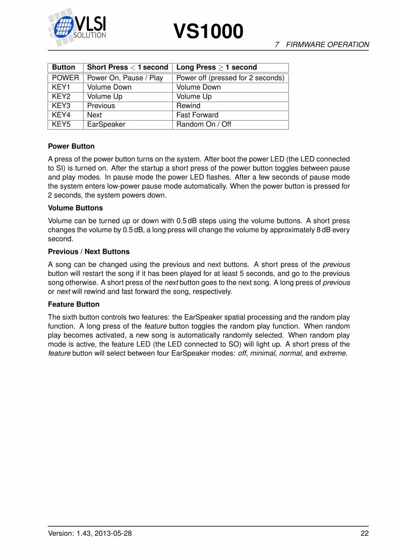
Button Short Press < 1 second Long Press ≥ 1 secondPOWER Power On, Pause / Play Power off (pressed for 2 seconds)KEY1 Volume Down Volume DownKEY2 Volume Up Volume UpKEY3 Previous RewindKEY4 Next Fast ForwardKEY5 EarSpeaker Random On / Off
Power Button
A press of the power button turns on the system. After boot the power LED (the LED connectedto SI) is turned on. After the startup a short press of the power button toggles between pauseand play modes. In pause mode the power LED flashes. After a few seconds of pause modethe system enters low-power pause mode automatically. When the power button is pressed for2 seconds, the system powers down.
Volume Buttons
Volume can be turned up or down with 0.5 dB steps using the volume buttons. A short presschanges the volume by 0.5 dB, a long press will change the volume by approximately 8 dB everysecond.
Previous / Next Buttons
A song can be changed using the previous and next buttons. A short press of the previousbutton will restart the song if it has been played for at least 5 seconds, and go to the previoussong otherwise. A short press of the next button goes to the next song. A long press of previousor next will rewind and fast forward the song, respectively.
Feature Button
The sixth button controls two features: the EarSpeaker spatial processing and the random playfunction. A long press of the feature button toggles the random play function. When randomplay becomes activated, a new song is automatically randomly selected. When random playmode is active, the feature LED (the LED connected to SO) will light up. A short press of thefeature button will select between four EarSpeaker modes: off, minimal, normal, and extreme.
Version: 1.43, 2013-05-28 22
VS10007 FIRMWARE OPERATION
7.5 Supported Audio Codecs
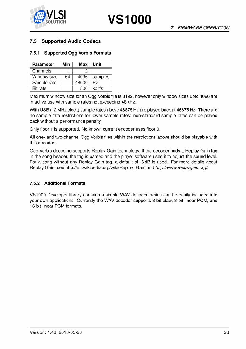
7.5.1 Supported Ogg Vorbis Formats
Parameter Min Max UnitChannels 1 2Window size 64 4096 samplesSample rate 48000 HzBit rate 500 kbit/s
Maximum window size for an Ogg Vorbis file is 8192, however only window sizes upto 4096 arein active use with sample rates not exceeding 48 kHz.
With USB (12 MHz clock) sample rates above 46875 Hz are played back at 46875 Hz. There areno sample rate restrictions for lower sample rates: non-standard sample rates can be playedback without a performance penalty.
Only floor 1 is supported. No known current encoder uses floor 0.
All one- and two-channel Ogg Vorbis files within the restrictions above should be playable withthis decoder.
Ogg Vorbis decoding supports Replay Gain technology. If the decoder finds a Replay Gain tagin the song header, the tag is parsed and the player software uses it to adjust the sound level.For a song without any Replay Gain tag, a default of -6 dB is used. For more details aboutReplay Gain, see http://en.wikipedia.org/wiki/Replay_Gain and http://www.replaygain.org/.
7.5.2 Additional Formats
VS1000 Developer library contains a simple WAV decoder, which can be easily included intoyour own applications. Currently the WAV decoder supports 8-bit ulaw, 8-bit linear PCM, and16-bit linear PCM formats.
Version: 1.43, 2013-05-28 23
VS10007 FIRMWARE OPERATION
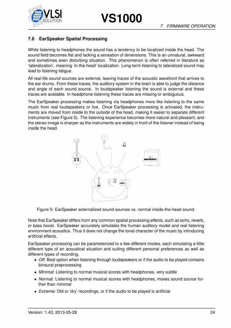
7.6 EarSpeaker Spatial Processing
While listening to headphones the sound has a tendency to be localized inside the head. Thesound field becomes flat and lacking a sensation of dimensions. This is an unnatural, awkwardand sometimes even disturbing situation. This phenomenon is often referred in literature as‘lateralization’, meaning ’in-the-head’ localization. Long-term listening to lateralized sound maylead to listening fatigue.
All real-life sound sources are external, leaving traces of the acoustic wavefront that arrives tothe ear drums. From these traces, the auditory system in the brain is able to judge the distanceand angle of each sound source. In loudspeaker listening the sound is external and thesetraces are available. In headphone listening these traces are missing or ambiguous.
The EarSpeaker processing makes listening via headphones more like listening to the samemusic from real loudspeakers or live. Once EarSpeaker processing is activated, the instru-ments are moved from inside to the outside of the head, making it easier to separate differentinstruments (see Figure 5). The listening experience becomes more natural and pleasant, andthe stereo image is sharper as the instruments are widely in front of the listener instead of beinginside the head.
Figure 5: EarSpeaker externalized sound sources vs. normal inside-the-head sound.
Note that EarSpeaker differs from any common spatial processing effects, such as echo, reverb,or bass boost. EarSpeaker accurately simulates the human auditory model and real listeningenvironment acoustics. Thus it does not change the tonal character of the music by introducingartificial effects.
EarSpeaker processing can be parameterized to a few different modes, each simulating a littledifferent type of an acoustical situation and suiting different personal preferences as well asdifferent types of recording.
• Off: Best option when listening through loudspeakers or if the audio to be played containsbinaural preprocessing
• Minimal: Listening to normal musical scores with headphones, very subtle
• Normal: Listening to normal musical scores with headphones, moves sound source fur-ther than minimal
• Extreme: Old or ’dry’ recordings, or if the audio to be played is artificial
Version: 1.43, 2013-05-28 24
VS10008 VS1000 ERRATA
8 VS1000 Errata
This chapter describes the known problems with different VS1000 revisions. Most of the prob-lems are correctable with user code that is loaded to IRAM.
VS1000b Changes• NAND FLASH and Ramdisk boot can have initialized Y data.• EarSpeaker initialization fixed, EarSpeaker optimized from 12 MHz to 10 MHz (at 44.1 kHz).• Small power-on click removed.• User interface works even if there is no filesystem. (You can turn the power off.)• NAND FLASH boot handles larger than 512-byte programs without a chain-loader rou-
tine (upto 8176 bytes). Ramdisk boot (VS1000_B.RUN) handles larger than 512-byteprograms (upto 8192 bytes).
• When attached to USB, LED is flashed when there is read/write activity. LED is turned offwhen the file system has been flushed.
• Volume is always initialized, USB Audio Device can be powered on while attached to USB(powered from VBUS).
• USB Suspend + Resume are implemented (but need user tuning).• Vorbis: Now uses adaptive accuracy for windowing, implements fast play mode, and has
better synchronization after non-fatal errors. Replay gain has been fixed.• Player: Fast play mode is used for better-sounding fast forward. Fast forward speeds up
when the ff button is kept pressed. Player uses the suspend routine to implement low-power pause mode. Timeout turns the unit off after being 5 minutes in pause mode. Thedefault maximum clock in player mode is 3.5×.
• Some new IRAM hooks: KeyEventHandler, MassStorage, USBSuspend, InitUSBDescrip-tors.
VS1000c Changes• No changes. Has the same firmware as version B.
VS1000b/c Errata• NAND FLASH and Ramdisk boot needs one filler word after every Y data record.• BusyWait1() wait time equals BusyWait10() time.• SCSI limited to 23-bit block address (4GB).• File scan gets stuck if FAT12 disk has subdirectories. FAT12 is not used if disk is > 16MB.
VS1000d Changes• Is backwards compatible with existing code, so can be used as a direct replacement
for VS1000b/c.• Code can be loaded and executed when in RAM disk mode without detaching the
device.• Default 3 V IO voltage setting reduced from 3.6 V to 3.3 V (control value 31 to 27).• SCSI supports the full 32-bit block address (2048GB).• BusyWait1() now waits 1 ms at 12 MHz clock.• Time to enter low-power pause mode doubled.• Ignores subdirectories in FAT12 disks.• RAMDISK label changed to VS1000D_RAM to make it possible to detect VS1000d.• USB descriptors, including device ID is the same as with VS1000b.• Fixed-width Latin-1 font (7x8 pixels) and 8-bit bit-reverse table added to YROM.
Version: 1.43, 2013-05-28 25
VS10009 DOCUMENT VERSION CHANGES
9 Document Version Changes
This chapter describes the most important changes to this document.
Version 1.43 for VS1000d, 2013-05-28
• Clarification to PWRBTN maximum voltage (IOVDD+0.3V).• Updated the example schematics in Section 5, Figure 3.
Version 1.42 for VS1000d, 2013-05-15
• GPIO1_4 and GPIO1_5 fixed in the chip symbol on the front page.
Version 1.41 for VS1000d, 2012-04-04
• Added Section 3.7, Power Button Characteristics.
Version 1.4 for VS1000d, 2011-10-06
• Fixed VS1000 symbol in the first page (RX is GPIO1_5).• Changed the suggested key pull-up and pull-down resistor values to 100 kΩ / 10 kΩ in
Section 5.
Version 1.3 for VS1000d, 2008-05-14
• Added VS1000d changes and removed VS1000A errata.
Version 1.2 for VS1000b/c, 2008-04-30
• Recommended operating conditions in section 3 clarified.
Version 1.1 for VS1000b/c, 2008-01-16
• Changed the default pull-up resistor on NFRDY to 10 kΩ. Consult your FLASH datasheet.• Example schematics updated.
Version 1.0 for VS1000b/c, 2007-09-11
• Production version.• Maximum and operational limits updated.
Version 0.4 for VS1000b/c, 2007-09-06
• Release for VS1000b / VS1000c.• Added VS1000 errata: Chapter 8.
Version 0.3, 2007-05-09
• Updated example schematic in Chapter 5.
Version: 1.43, 2013-05-28 26
VS100010 CONTACT INFORMATION
10 Contact Information
VLSI Solution OyEntrance G, 2nd floor
Hermiankatu 8FI-33720 Tampere
FINLAND
Fax: +358-3-3140-8288Phone: +358-3-3140-8200
Commercial e-mail: [email protected]: http://www.vlsi.fi/
For technical support or suggestions regarding this document, please participate athttp://www.vsdsp-forum.com/
For confidential technical discussions, [email protected]
Version: 1.43, 2013-05-28 27