Embed Size (px)
Citation preview

aADF4001
One Technology Way, P.O. Box 9106, Norwood, MA 02062-9106, U.S.A.
Tel: 781/329-4700 www.analog.com
Fax: © Analog Devices, Inc. All rights reserved.
Information furnished by Analog Devices is believed to be accurate andreliable. However, no responsibility is assumed by Analog Devices for itsuse, nor for any infringements of patents or other rights of third parties thatmay result from its use. No license is granted by implication or otherwiseunder any patent or patent rights of Analog Devices. Trademarks andregistered trademarks are the property of their respective owners.
REV.
200 MHz Clock Generator PLL
FUNCTIONAL BLOCK DIAGRAM
RFINA
RFINB
13-BITN COUNTER
LOCK DETECT CURRENTSETTING 1
CPI3 CPI2 CPI1 CPI6 CPI5 CPI4
M1M3 M2
SDOUT
AVDD
REFIN
CLK
DATA
LE
AVDD DVDD VP CPGND RSET
14-BITR COUNTER
R COUNTERLATCH
FUNCTIONLATCH
24-BITINPUT REGISTER
N COUNTERLATCH
SDOUT
22
14
ADF4001
MUXOUTMUX
HIGH Z
CURRENTSETTING 2
CHARGEPUMP
CP
CE AGND DGND
PHASEFREQUENCYDETECTOR
REFERENCE
13
FEATURES
200 MHz Bandwidth
2.7 V to 5.5 V Power Supply
Separate Charge Pump Supply (VP) Allows Extended
Tuning Voltage in 5 V Systems
Programmable Charge Pump Currents
3-Wire Serial Interface
Hardware and Software Power-Down Mode
Analog and Digital Lock Detect
Hardware Compatible to the ADF4110/ADF4111/
ADF4112/ADF4113
Typical Operating Current 4.5 mA
Ultralow Phase Noise
16-Lead TSSOP
20-Lead LFCSP
APPLICATIONS
Clock Generation
Low Frequency PLLs
Low Jitter Clock Source
Clock Smoothing
Frequency Translation
SONET, ATM, ADM, DSLAM, SDM
GENERAL DESCRIPTIONThe ADF4001 clock generator can be used to implement clocksources for PLLs that require very low noise, stable referencesignals. It consists of a low noise digital PFD (phase frequencydetector), a precision charge pump, a programmable referencedivider, and a programmable 13-bit N counter. In addition, the14-bit reference counter (R counter) allows selectable REFIN
frequencies at the PFD input. A complete PLL (phase-lockedloop) can be implemented if the synthesizer is used with an exter-nal loop filter and VCO (voltage controlled oscillator) orVCXO (voltage controlled crystal oscillator). The N minimumvalue of 1 allows flexibility in clock generation.
2013781/461-3113
B

ADF4001* PRODUCT PAGE QUICK LINKSLast Content Update: 02/23/2017
COMPARABLE PARTSView a parametric search of comparable parts.
EVALUATION KITS• ADF4001 Evaluation Board
DOCUMENTATIONApplication Notes
• AN-30: Ask the Applications Engineer - PLL Synthesizers
• AN-873: Lock Detect on the ADF4xxx Family of PLL Synthesizers
Data Sheet
• ADF4001: 200 MHz Clock Generator PLL Data Sheet
User Guides
• UG-092: The PLL Frequency Synthesizer Evaluation Board for the ADF4001
• UG-476: PLL Software Installation Guide
SOFTWARE AND SYSTEMS REQUIREMENTS• ADF4001 FMC-SDP Interposer & Evaluation Board / Xilinx
KC705 Reference Design
• BeMicro FPGA Project for ADF4001 with Nios driver
TOOLS AND SIMULATIONS• ADIsimPLL™
• ADIsimRF
REFERENCE MATERIALSTechnical Articles
• Phase Locked Loops for High-Frequency Receivers and Transmitters – Part 1
• Phase Locked Loops for High-Frequency Receivers and Transmitters – Part 3
• Phase-Locked Loops for High-Frequency Receivers and Transmitters - Part 2
DESIGN RESOURCES• ADF4001 Material Declaration
• PCN-PDN Information
• Quality And Reliability
• Symbols and Footprints
DISCUSSIONSView all ADF4001 EngineerZone Discussions.
SAMPLE AND BUYVisit the product page to see pricing options.
TECHNICAL SUPPORTSubmit a technical question or find your regional support number.
DOCUMENT FEEDBACKSubmit feedback for this data sheet.
This page is dynamically generated by Analog Devices, Inc., and inserted into this data sheet. A dynamic change to the content on this page will not trigger a change to either the revision number or the content of the product data sheet. This dynamic page may be frequently modified.

REV. –2–
ADF4001–SPECIFICATIONS1(AVDD = DVDD = 3 V 10%, 5 V 10%; AVDD ≤ VP ≤ 6.0 V ; AGND = DGND =
CPGND = 0 V; RSET = 4.7 k; TA = TMIN to TMAX, unless otherwise noted; dBm referred to 50 .)
Parameter B Version Unit Test Conditions/Comments
RF CHARACTERISTICS (3 V) See Figure 3 for Input CircuitRF Input Frequency 5/165 MHz min/maxRF Input Sensitivity –10/0 dBm min/max
RF CHARACTERISTICS (5 V)RF Input Frequency 10/200 MHz min/max –5/0 dBm min/max
20/200 MHz min/max –10/0 dBm min/max
REFIN CHARACTERISTICS See Figure 2 for Input CircuitREFIN Input Frequency 5/104 MHz min/max For f < 5 MHz, Use DC-Coupled Square Wave
(0 to VDD)REFIN Input Sensitivity2 –5 dBm min AC-Coupled. When DC-Coupled:
0 to VDD Max (CMOS Compatible)REFIN Input Capacitance 10 pF maxREFIN Input Current ±100 µA max
PHASE DETECTORPhase Detector Frequency3 55 MHz max
CHARGE PUMPICP Sink/Source Programmable: See Table V
High Value 5 mA typ With RSET = 4.7 kΩLow Value 625 µA typAbsolute Accuracy 2.5 % typ With RSET = 4.7 kΩRSET Range 2.7/10 kΩ typ See Table V
ICP Three-State Leakage Current 1 nA typSink and Source Current Matching 2 % typ 0.5 V ≤ VCP ≤ VP – 0.5ICP vs. VCP 1.5 % typ 0.5 V ≤ VCP ≤ VP – 0.5ICP vs. Temperature 2 % typ VCP = VP/2
LOGIC INPUTSVINH, Input High Voltage 0.8 × DVDD V minVINL, Input Low Voltage 0.2 × DVDD V maxIINH/IINL, Input Current ±1 µA maxCIN, Input Capacitance 10 pF max
LOGIC OUTPUTSVOH, Output High Voltage DVDD – 0.4 V min IOH = 500 µAVOL, Output Low Voltage 0.4 V max IOL = 500 µA
POWER SUPPLIESAVDD 2.7/5.5 V min/V maxDVDD AVDD
VP AVDD/6.0 V min/V max AVDD ≤ VP ≤ 6.0 VIDD
4 (AIDD + DIDD)ADF4001 5.5 mA max 4.5 mA typical
IP 0.4 mA max TA = 25°CLow Power Sleep Mode 1 µA typ
NOISE CHARACTERISTICSADF4001 Phase Noise Floor5 –161 dBc/Hz typ @ 200 kHz PFD Frequency
–153 dBc/Hz typ @ 1 MHz PFD FrequencyPhase Noise Performance6 @ VCXO Output
200 MHz Output7 –99 dBc/Hz typ @ 1 kHz Offset and 200 kHz PFD Frequency Spurious Signals
200 MHz Output7 –90/–95 dBc typ/dBc typ @ 200 kHz/400 kHz and 200 kHz PFD Frequency
NOTES1Operating temperature range (B Version) is –40°C to +85°C.2AVDD = DVDD = 3 V; for AVDD = DVDD = 5 V, use CMOS compatible levels.3Guaranteed by design. Sample tested to ensure compliance.4TA = 25°C; AVDD = DVDD = 3 V; RFIN = 100 MHz.5The synthesizer phase noise floor is estimated by measuring the in-band phase noise at the output of the VCO and subtracting 20 logN (where N is the N divider value).6The phase noise is measured with the EVAL-ADF4001EB1 evaluation board and the HP8562E spectrum analyzer.7fREFIN
= 10 MHz; fPFD = 200 kHz; Offset Frequency = 1 kHz; fRF = 200 MHz; N = 1000; Loop B/W = 20 kHz.
Specifications subject to change without notice.
B

REV. –3–
ADF4001
TIMING CHARACTERISTICS
Limit atTMIN to TMAX
Parameter (B Version) Unit Test Conditions/Comments
t1 10 ns min DATA to CLOCK Setup Timet2 10 ns min DATA to CLOCK Hold Timet3 25 ns min CLOCK High Durationt4 25 ns min CLOCK Low Durationt5 10 ns min CLOCK to LE Setup Timet6 20 ns min LE Pulsewidth
Guaranteed by design but not production tested.Specifications subject to change without notice.
(AVDD = DVDD = 3 V 10%, 5 V 10%; AVDD ≤ VP ≤ 6.0 V ; AGND = DGND = CPGND= 0 V;RSET = 4.7 k; TA = TMIN to TMAX, unless otherwise noted; dBm referred to 50 .)
t1 t2
t3 t4
t6
t5
DB20(MSB) DB19 DB2
DB1(CONTROL BIT C2)
CLOCK
DATA
LE
LE
DB0 (LSB)(CONTROL BIT C1)
Figure 1. Timing Diagram
ABSOLUTE MAXIMUM RATINGS1, 2
(TA = 25°C, unless otherwise noted.)
AVDD to GND3 . . . . . . . . . . . . . . . . . . . . . . . . –0.3 V to +7 VAVDD to DVDD . . . . . . . . . . . . . . . . . . . . . . . . . 0 V to +0.3 VVP to GND . . . . . . . . . . . . . . . . . . . . . . . . . . . –0.3 V to +7 VVP to AVDD . . . . . . . . . . . . . . . . . . . . . . . . . . –0.3 V to +5.5 VDigital I/O Voltage to GND . . . . . . . . . –0.3 V to VDD + 0.3 VAnalog I/O Voltage to GND . . . . . . . . . . –0.3 V to VP + 0.3 VREFIN, RFINA, RFINB to GND . . . . . . . –0.3 V to VDD + 0.3 VRFINA to RFINB . . . . . . . . . . . . . . . . . . . . . . . . . . . . ± mVOperating Temperature Range
Industrial (B Version) . . . . . . . . . . . . . . . . –40°C to +85°CStorage Temperature Range . . . . . . . . . . . . –65°C to +150°CMaximum Junction Temperature . . . . . . . . . . . . . . . . . .150°C
TSSOP θJA Thermal Impedance . . . . . . . . . . . . . . 150.4°C/WLFCSP θJA Thermal Impedance (Paddle Soldered) . . 122°C/WLFCSP θJA Thermal Impedance (Paddle Not Soldered) 216°C/WLead Temperature, Soldering
Vapor Phase (60 sec) . . . . . . . . . . . . . . . . . . . . . . . . . 215°CInfrared (15 sec) . . . . . . . . . . . . . . . . . . . . . . . . . . . . . 220°C
NOTES1Stresses above those listed under Absolute Maximum Ratings may cause perma-
nent damage to the device. This is a stress rating only; functional operation of thedevice at these or any other conditions above those listed in the operationalsections of this specification is not implied. Exposure to absolute maximum ratingconditions for extended periods may affect device reliability.
2This device is a high performance RF integrated circuit with an ESD rating of<2 kΩ and it is ESD sensitive. Proper precautions should be taken for handling andassembly.
3GND = AGND = DGND = 0 V.
CAUTIONESD (electrostatic discharge) sensitive device. Electrostatic charges as high as 4000 V readilyaccumulate on the human body and test equipment and can discharge without detection. Althoughthe ADF4001 features proprietary ESD protection circuitry, permanent damage may occur ondevices subjected to high energy electrostatic discharges. Therefore, proper ESD precautions arerecommended to avoid performance degradation or loss of functionality.
WARNING!
ESD SENSITIVE DEVICE
B
600
ADF4001
Rev. B | Page 4
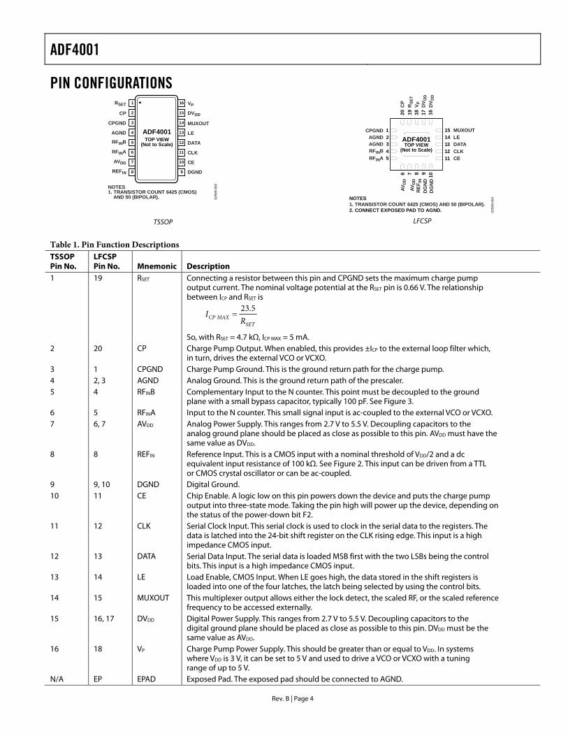
PIN CONFIGURATIONS
TSSOP LFCSP
Table 1. Pin Function Descriptions TSSOP Pin No.
LFCSP Pin No. Mnemonic Description
1 19 RSET Connecting a resistor between this pin and CPGND sets the maximum charge pump output current. The nominal voltage potential at the RSET pin is 0.66 V. The relationship between ICP and RSET is
SETMAXCP R
I5.23
So, with RSET = 4.7 kΩ, ICP MAX = 5 mA. 2 20 CP Charge Pump Output. When enabled, this provides ±ICP to the external loop filter which,
in turn, drives the external VCO or VCXO. 3 1 CPGND Charge Pump Ground. This is the ground return path for the charge pump. 4 2, 3 AGND Analog Ground. This is the ground return path of the prescaler. 5 4 RFINB Complementary Input to the N counter. This point must be decoupled to the ground
plane with a small bypass capacitor, typically 100 pF. See Figure 3. 6 5 RFINA Input to the N counter. This small signal input is ac-coupled to the external VCO or VCXO. 7 6, 7 AVDD Analog Power Supply. This ranges from 2.7 V to 5.5 V. Decoupling capacitors to the
analog ground plane should be placed as close as possible to this pin. AVDD must have the same value as DVDD.
8 8 REFIN Reference Input. This is a CMOS input with a nominal threshold of VDD/2 and a dc equivalent input resistance of 100 kΩ. See Figure 2. This input can be driven from a TTL or CMOS crystal oscillator or can be ac-coupled.
9 9, 10 DGND Digital Ground. 10 11 CE Chip Enable. A logic low on this pin powers down the device and puts the charge pump
output into three-state mode. Taking the pin high will power up the device, depending on the status of the power-down bit F2.
11 12 CLK Serial Clock Input. This serial clock is used to clock in the serial data to the registers. The data is latched into the 24-bit shift register on the CLK rising edge. This input is a high impedance CMOS input.
12 13 DATA Serial Data Input. The serial data is loaded MSB first with the two LSBs being the control bits. This input is a high impedance CMOS input.
13 14 LE Load Enable, CMOS Input. When LE goes high, the data stored in the shift registers is loaded into one of the four latches, the latch being selected by using the control bits.
14 15 MUXOUT This multiplexer output allows either the lock detect, the scaled RF, or the scaled reference frequency to be accessed externally.
15 16, 17 DVDD Digital Power Supply. This ranges from 2.7 V to 5.5 V. Decoupling capacitors to the digital ground plane should be placed as close as possible to this pin. DVDD must be the same value as AVDD.
16 18 VP Charge Pump Power Supply. This should be greater than or equal to VDD. In systems where VDD is 3 V, it can be set to 5 V and used to drive a VCO or VCXO with a tuning range of up to 5 V.
N/A EP EPAD Exposed Pad. The exposed pad should be connected to AGND.
RSET
CP
CPGND
AGND
RFINB
RFINA
AVDD
REFIN
LE
MUXOUT
DVDD
VP
CE
CLK
DATA
DGND
NOTES1. TRANSISTOR COUNT 6425 (CMOS)
AND 50 (BIPOLAR).
TOP VIEW(Not to Scale)
1
2
3
4
5
6
7
8
ADF4001
16
15
14
13
12
11
10
9
0256
9-0
03
AGND
MUXOUT
LE
DATA
CLK
CE
AV
DD
AV
DD
RE
FIN
DG
ND
DG
ND
CP
RS
ET
VP
DV
DD
DV
DD
CPGND
AGNDRFINB
RFINA
NOTES1. TRANSISTOR COUNT 6425 (CMOS) AND 50 (BIPOLAR).2. CONNECT EXPOSED PAD TO AGND.
14
13
12
1
3
4
15
11
2
5
76 8 9
10
1920 18 17 16
ADF4001TOP VIEW
(Not to Scale)
025
69-0
04

REV. –5–
Typical Performance Characteristics–ADF4001
FREQUENCY – MHz
0
0
AM
PL
ITU
DE
– d
Bm
–5
–10
–15
–20
–25
–30
–3550 100 150 200 250
TA = +25C
TA = +85C
TA = –40C
TPC 1. Input Sensitivity, VDD = 3.3 V, 100 pF on RFIN
FREQUENCY – MHz
0
0
AM
PL
ITU
DE
– d
Bm
–5
–10
–15
–20
–25
–305 10 15 20 25
TPC 2. Input Sensitivity, VDD = 3.3 V, 100 pF on RFIN
0
–10
–20
–30
–40
–50
–60
–70
–80
–90
–100
OU
TP
UT
PO
WE
R –
dB
–2kHz –1kHz 200MHz 1kHz 2kHz 0
REFERENCE LEVEL = –5.7dBm
VDD = 3V, VP = 5VICP = 2.5mAPFD FREQUENCY = 200kHzLOOP BANDWIDTH = 20kHzRES. BANDWIDTH = 10HzVIDEO BANDWIDTH = 10HzSWEEP = 1.9 SECONDSAVERAGES = 26
–99.2dBc/Hz
TPC 3. Phase Noise (200 MHz, 200 kHz, 20 kHz)
FREQUENCY OFFSET FROM 200MHz CARRIER – Hz
–40
100
PH
AS
E N
OIS
E –
dB
c/H
z
–50
–60
–70
–80
–90
–100
–110
–120
–130
–1401k 10k 100k 1M
0.229 rms
10dB/DIVISION RL = –40dBc/Hz rms NOISE = 0.229 DEGREES
TPC 4. Integrated Phase Noise (200 MHz, 200 kHz, 20 kHz)
0
–10
–20
–30
–40
–50
–60
–70
–80
–90
–100
OU
TP
UT
PO
WE
R –
dB
–200kHz –100kHz 0200MHz 100kHz 200kHz
VDD = 3V, VP = 5VICP = 2.5mAPFD FREQUENCY = 200kHzLOOP BANDWIDTH = 20kHzRES. BANDWIDTH = 300HzVIDEO BANDWIDTH = 300HzSWEEP = 4.2 SECONDSAVERAGES = 20
REFERENCE LEVEL =–5.7dBm
–92.3dBc
TPC 5. Reference Spurs (200 MHz, 200 kHz, 20 kHz)
B

REV.
ADF4001
–6–
CIRCUIT DESCRIPTIONReference Input SectionThe reference input stage is shown in Figure 2. SW1 and SW2are normally closed switches. SW3 is normally open. Whenpower-down is initiated, SW3 is closed and SW1 and SW2 areopened. This ensures that there is no loading of the REFIN pinon power-down.
POWER-DOWNCONTROL
TOR COUNTERNC
NO
SW1
SW3
SW2
NC 100k
REFINBUFFER
Figure 2. Reference Input Stage
RF Input StageThe RF input stage is shown in Figure 3. It is followed by atwo-stage limiting amplifier to generate the CML clock levelsneeded for the N counter buffer.
RFINB
RFINA
2k
AGND
AVDD
BIASGENERATOR
2k
1.6V
Figure 3. RF Input Stage
N CounterThe N CMOS counter allows a wide ranging division ratioin the PLL feedback counter. Division ratios of 1 to 8191are allowed.
N and R RelationshipThe N counter with the R counter make it possible to generateoutput frequencies that are spaced only by the reference fre-quency divided by R. The equation for the VCO frequency is
f N R fVCO REFIN= ×
fVCO is the output frequency of the external voltage cotrolledoscillator (VCO).
N is the preset divide ratio of the binary 13-bit counter(1 to 8,191).
fREFIN is the external reference frequency oscillator.
R is the preset divide ratio of the binary 14-bit programmablereference counter (1 to 16,383).
TO PFD
13-BIT NCOUNTER
FROMN COUNTER LATCH
FROM RFINPUT STAGE
Figure 4. N Counter
R CounterThe 14-bit R counter allows the input reference frequency to bedivided down to produce the reference clock to the phase frequencydetector (PFD). Division ratios from 1 to 16,383 are allowed.
PHASE FREQUENCY DETECTOR (PFD) ANDCHARGE PUMPThe PFD takes inputs from the R counter and N counter andproduces an output proportional to the phase and frequencydifference between them. Figure 5 is a simplified schematic.The PFD includes a programmable delay element that controlsthe width of the antibacklash pulse. This pulse ensures that nodead zone is in the PFD transfer function and minimizes phasenoise and reference spurs. Two bits in the reference counterlatch, ABP2 and ABP1, control the width of the pulse (seeTable III).
DELAY
R DIVIDER
N DIVIDER
CP OUTPUT
HI
HI
CPGND
VP CHARGEPUMP
UP
CP
DOWN
N DIVIDER
R DIVIDER
D1 Q1
U1
CLR1
D2
CLR2
Q2
U2
U3
Figure 5. PFD Simplified Schematic and Timing (In Lock)
MUXOUT AND LOCK DETECTThe output multiplexer on the ADF4001 family allows theuser to access various internal points on the chip. The state ofMUXOUT is controlled by M3, M2, and M1 in the functionlatch. Table V shows the full truth table. Figure 6 shows theMUXOUT section in block diagram form.
B

REV.
ADF4001
–7–
ANALOG LOCK DETECT
DIGITAL LOCK DETECT
R COUNTER OUTPUT
N COUNTER OUTPUT
SDOUT
DGND
DVDD
CONTROL MUXOUTMUX
Figure 6. MUXOUT Circuit
Lock DetectMUXOUT can be programmed for two types of lock detect:digital lock detect and analog lock detect. Digital lock detect isactive high. When LDP in the R counter latch is set to 0, digitallock detect is set high when the phase error on three consecutivephase detector cycles is less than 15 ns. With LDP set to 1, fiveconsecutive cycles of less than 15 ns are required to set the lockdetect. It will stay set high until a phase error of greater than
25 ns is detected on any subsequent PD cycle. The N-channelopen-drain analog lock detect should be operated with an externalpull-up resistor of 10 kΩ nominal. When lock has been detected,this output will be high with narrow low-going pulses.
INPUT SHIFT REGISTERThe ADF4001 digital section includes a 24-bit input shift regis-ter, a 14-bit R counter, and a 13-bit N counter. Data is clockedinto the 24-bit shift register on each rising edge of CLK. Thedata is clocked in MSB first. Data is transferred from the shiftregister to one of four latches on the rising edge of LE. Thedestination latch is determined by the state of the two controlbits (C2, C1) in the shift register. These are the two LSBs, DB1and DB0, as shown in the timing diagram of Figure 1. The truthtable for these bits is shown in Table I. Table II shows a sum-mary of how the latches are programmed.
Table I. C2, C1 Truth Table
Control BitsC2 C1 Data Latch
0 0 R Counter0 1 N Counter1 0 Function Latch1 1 Initialization Latch
Table II. ADF4001 Family Latch Summary
REFERENCE COUNTER LATCH
DB20 DB19 DB18 DB17 DB16 DB15 DB14 DB13 DB12 DB11 DB10 DB9 DB8 DB7 DB6 DB5 DB4 DB3 DB2 DB1 DB0
C2 (0) C1 (0)R1R2R3R4R5R7R14ABP1T2LDP R13 R6
CONTROLBITS
ABP2T1
DB21
R12 R11 R10
DB22DB23
R8R9
RESERVED
LO
CK
DE
TE
CT
PR
EC
ISIO
N
TESTMODEBITS
ANTI-BACKLASH
WIDTH14-BIT REFERENCE COUNTER
X X X
DB20 DB19 DB18 DB17 DB16 DB15 DB14 DB13 DB12 DB11 DB10 DB9 DB8 DB7 DB6 DB5 DB4 DB3 DB2 DB1 DB0
C2 (1) C1 (1)F1PD1M1M2M3F3CPI1CPI2CPI5CPI6 TC4PD2 F2
CONTROLBITS
CO
UN
TE
RR
ES
ET
PO
WE
R-
DO
WN
1
MUXOUTCONTROL
PH
AS
ED
ET
EC
TO
RP
OL
AR
ITY
CP
TH
RE
E-
ST
AT
E
PO
WE
R-
DO
WN
2 CURRENTSETTING
1
TIMER COUNTERCONTROL
CPI3CPI4
DB21
CURRENTSETTING
2
TC3 TC2 TC1
DB22DB23
FAS
TL
OC
KE
NA
BL
E
FA
ST
LO
CK
MO
DE
F4F5
RESERVED
X = DON’T CARE
X X
DB20 DB19 DB18 DB17 DB16 DB15 DB14 DB13 DB12 DB11 DB10 DB9 DB8 DB7 DB6 DB5 DB4 DB3 DB2 DB1 DB0
C2 (0) C1 (1)N1N8N9N12N13 N7G1
CONTROLBITS
N10N11
DB21
N6 N5 N4
DB22DB23
N2N3
RESERVEDCP
GAIN RESERVED13-BIT N COUNTER
X X X X X X X X
DB20 DB19 DB18 DB17 DB16 DB15 DB14 DB13 DB12 DB11 DB10 DB9 DB8 DB7 DB6 DB5 DB4 DB3 DB2 DB1 DB0
C2 (1) C1 (0)F1PD1M1M2M3F3CPI1CPI2CPI5CPI6 TC4PD2 F2
CONTROLBITS
CO
UN
TE
RR
ES
ET
PO
WE
R-
DO
WN
1
MUXOUTCONTROL
PH
AS
ED
ET
EC
TO
RP
OL
AR
ITY
CP
TH
RE
E-
ST
AT
E
PO
WE
R-
DO
WN
2 CURRENTSETTING
1
TIMER COUNTERCONTROL
CPI3CPI4
DB21
CURRENTSETTING
2
TC3 TC2 TC1
DB22DB23
FAS
TL
OC
KE
NA
BL
E
FA
ST
LO
CK
MO
DE
F4F5
RESERVED
X X
N COUNTER LATCH
FUNCTION LATCH
INITIALIZATION LATCH
B

REV.
ADF4001
–8–
Table III. Reference Counter Latch Map
LDP OPERATION
0 THREE CONSECUTIVE CYCLES OF PHASE DELAY LESS THAN15ns MUST OCCUR BEFORE LOCK DETECT IS SET.
1 FIVE CONSECUTIVE CYCLES OF PHASE DELAY LESS THAN15ns MUST OCCUR BEFORE LOCK DETECT IS SET.
ABP2 ABP1 ANTIBACKLASH PULSE WIDTH
0 0 2.9ns0 1 1.3ns1 0 6.0ns1 1 2.9ns
R14 R13 R12 .......... R3 R2 R1 DIVIDE RATIO
0 0 0 .......... 0 0 1 10 0 0 .......... 0 1 0 20 0 0 .......... 0 1 1 30 0 0 .......... 1 0 0 4. . . .......... . . . .. . . .......... . . . .. . . .......... . . . .1 1 1 .......... 1 0 0 16380
1 1 1 .......... 1 0 1 16381
1 1 1 .......... 1 1 0 16382
1 1 1 .......... 1 1 1 16383
TEST MODE BITS SHOULDBE SET TO 00 FOR NORMAL
OPERATION
DB20 DB19 DB18 DB17 DB16 DB15 DB14 DB13 DB12 DB11 DB10 DB9 DB8 DB7 DB6 DB5 DB4 DB3 DB2 DB1 DB0
C2 (0) C1 (0)R1R2R3R4R5R7R14ABP1T2LDP R13 R6
CONTROLBITS
ABP2T1
DB21
R12 R11 R10
DB22DB23
R8R9
RESERVEDL
OC
KD
ET
EC
TP
RE
CIS
ION
TESTMODEBITS
ANTI-BACKLASH
WIDTH14-BIT REFERENCE COUNTER
X X X
X = DON’T CARE
B

REV.
ADF4001
–9–
Table IV. N Counter Latch Map
THESE BITS ARE NOT USEDBY THE DEVICE AND ARE
DON’T CARE BITS.
F4 (FUNCTION LATCH)FASTLOCK ENABLE CP GAIN OPERATION
0 0 CHARGE PUMP CURRENT SETTING1 IS PERMANENTLY USED
0 1 CHARGE PUMP CURRENT SETTING2 IS PERMANENTLY USED
1 0 CHARGE PUMP CURRENT SETTING1 IS USED
1 1 CHARGE PUMP CURRENT ISSWITCHED TO SETTING 2. THETIME SPENT IN SETTING 2 ISDEPENDENT ON WHICH FASTLOCKMODE IS USED. SEE FUNCTION
LATCH DESCRIPTION.
N13 N12 N11 N3 N2 N1 N COUNTER DIVIDE RATIO
0 0 0 .......... 0 0 1 10 0 0 .......... 0 1 0 20 0 0 .......... 0 1 1 30 0 0 .......... 1 0 0 4. . . .......... . . . .. . . .......... . . . .. . . .......... . . . .1 1 1 .......... 1 0 0 8188
1 1 1 .......... 1 0 1 8189
1 1 1 .......... 1 1 0 8190
1 1 1 .......... 1 1 1 8191
DB20 DB19 DB18 DB17 DB16 DB15 DB14 DB13 DB12 DB11 DB10 DB9 DB8 DB7 DB6 DB5 DB4 DB3 DB2 DB1 DB0
C2 (0) C1 (1)N1N2N3N4N5N6N7N8N9N10N11N12N13
CONTROLBITSRESERVED13-BIT N COUNTER
DB21
RESERVED
DB22DB23
CP
GA
IN
G1
X = DON’T CARE
X X X X X X X X
B

REV.
ADF4001
–10–
Table V. Function Latch Map
DB20 DB19 DB18 DB17 DB16 DB15 DB14 DB13 DB12 DB11 DB10 DB9 DB8 DB7 DB6 DB5 DB4 DB3 DB2 DB1 DB0
C2 (1) C1 (0)F1PD1M1M2M3F3CPI1CPI2CPI5CPI6 TC4PD2 F2
CONTROLBITS
CO
UN
TE
RR
ES
ET
PO
WE
R-
DO
WN
1
MUXOUTCONTROL
PH
AS
ED
ET
EC
TO
RP
OL
AR
ITY
CP
TH
RE
E-
ST
AT
E
PO
WE
R-
DO
WN
2 CURRENTSETTING
1
TIMER COUNTERCONTROL
CPI3CPI4
DB21
CURRENTSETTING
2
TC3 TC2 TC1
DB22DB23
FA
ST
LO
CK
EN
AB
LE
FA
ST
LO
CK
MO
DE
F4F5
RESERVED
CE PIN PD2 PD1 MODE
0 X X ASYNCHRONOUS POWER-DOWN1 X 0 NORMAL OPERATION1 0 1 ASYNCHRONOUS POWER-DOWN1 1 1 SYNCHRONOUS POWER-DOWN
CPI6 CPI5 CP14 ICP (mA)
CPI3 CPI2 CPI1 2.7k 4.7k 10k
0 0 0 1.088 0.625 0.2940 0 1 2.176 1.25 0.5880 1 0 3.264 1.875 0.8820 1 1 4.352 2.5 1.1761 0 0 5.44 3.125 1.471 0 1 6.528 3.75 1.7641 1 0 7.616 4.375 2.0581 1 1 8.704 5.0 2.352
TIMEOUTTC4 TC3 TC2 TC1 (PFD CYCLES)
0 0 0 0 30 0 0 1 70 0 1 0 110 0 1 1 150 1 0 0 190 1 0 1 230 1 1 0 270 1 1 1 311 0 0 0 351 0 0 1 391 0 1 0 431 0 1 1 471 1 0 0 511 1 0 1 551 1 1 0 591 1 1 1 63
F4 F5 FASTLOCK MODE
0 X FASTLOCK DISABLED1 0 FASTLOCK MODE 11 1 FASTLOCK MODE 2
F3 CHARGE PUMP OUTPUT
0 NORMAL
1 THREE-STATE
M3 M2 M1 OUTPUT
0 0 0 THREE-STATE OUTPUT0 0 1 DIGITAL LOCK DETECT0 1 0 N DIVIDER OUTPUT0 1 1 AVDD1 0 0 R DIVIDER OUTPUT1 0 1 N-CHANNEL OPEN-DRAIN
LOCK DETECT1 1 0 SERIAL DATA OUTPUT1 1 1 DGND
PHASE DETECTORF2 POLARITY0 NEGATIVE1 POSITIVE
COUNTER F1 OPERATION
0 NORMAL 1 R, N COUNTER
HELD IN RESET
X = DON’T CARE
X X
B

REV.
ADF4001
–11–
Table VI. Initialization Latch Map
DB20 DB19 DB18 DB17 DB16 DB15 DB14 DB13 DB12 DB11 DB10 DB9 DB8 DB7 DB6 DB5 DB4 DB3 DB2 DB1 DB0
C2 (1) C1 (1)F1PD1M1M2M3F3CPI1CPI2CPI5CPI6 TC4PD2 F2
CONTROLBITS
CO
UN
TE
RR
ES
ET
PO
WE
R-
DO
WN
1
MUXOUTCONTROL
PH
AS
ED
ET
EC
TO
RP
OL
AR
ITY
CP
TH
RE
E-
ST
AT
E
PO
WE
R-
DO
WN
2 CURRENTSETTING
1
TIMER COUNTERCONTROL
CPI3CPI4
DB21
CURRENTSETTING
2
TC3 TC2 TC1
DB22DB23
FA
ST
LO
CK
EN
AB
LE
FA
ST
LO
CK
MO
DE
F4F5
RESERVED
CE PIN PD2 PD1 MODE
0 X X ASYNCHRONOUS POWER-DOWN1 X 0 NORMAL OPERATION1 0 1 ASYNCHRONOUS POWER-DOWN1 1 1 SYNCHRONOUS POWER-DOWN
CPI6 CPI5 CP14 ICP (mA)
CPI3 CPI2 CPI1 2.7k 4.7k 10k
0 0 0 1.088 0.625 0.2940 0 1 2.176 1.25 0.5880 1 0 3.264 1.875 0.8820 1 1 4.352 2.5 1.1761 0 0 5.44 3.125 1.471 0 1 6.528 3.75 1.7641 1 0 7.616 4.375 2.0581 1 1 8.704 5.0 2.352
TIMEOUTTC4 TC3 TC2 TC1 (PFD CYCLES)
0 0 0 0 30 0 0 1 70 0 1 0 110 0 1 1 150 1 0 0 190 1 0 1 230 1 1 0 270 1 1 1 311 0 0 0 351 0 0 1 391 0 1 0 431 0 1 1 471 1 0 0 511 1 0 1 551 1 1 0 591 1 1 1 63
F4 F5 FASTLOCK MODE
0 X FASTLOCK DISABLED1 0 FASTLOCK MODE 11 1 FASTLOCK MODE 2
F3 CHARGE PUMP OUTPUT
0 NORMAL
1 THREE-STATE
M3 M2 M1 OUTPUT
0 0 0 THREE-STATE OUTPUT0 0 1 DIGITAL LOCK DETECT0 1 0 N DIVIDER OUTPUT0 1 1 AVDD1 0 0 R DIVIDER OUTPUT1 0 1 N-CHANNEL OPEN-DRAIN
LOCK DETECT1 1 0 SERIAL DATA OUTPUT1 1 1 DGND
PHASE DETECTORF2 POLARITY0 NEGATIVE1 POSITIVE
COUNTER F1 OPERATION
0 NORMAL 1 R, N COUNTER
HELD IN RESET
X = DON’T CARE
X X
B

REV.
ADF4001
–12–
FUNCTION LATCHWith C2, C1 set to 1, 0, the on-chip function latch will be pro-grammed. Table V shows the input data format for programmingthe function latch.
Counter ResetDB2 (F1) is the counter reset bit. When this is 1, the R counterand the A, B counters are reset. For normal operation, this bitshould be 0. Upon powering up, the F1 bit needs to be disabled,and the N counter resumes counting in close alignment with theR counter. (The maximum error is one prescaler cycle.)
Power-DownDB3 (PD1) and DB21 (PD2) on the ADF4001 family provideprogrammable power-down modes. They are enabled by theCE pin.
When the CE pin is low, the device is immediately disabledregardless of the states of PD2, PD1.
In the programmed asynchronous power-down, the device pow-ers down immediately after latching a 1 into Bit PD1, with thecondition that PD2 has been loaded with a 0.
In the programmed synchronous power-down, the device power-down is gated by the charge pump to prevent unwanted frequencyjumps. Once the power-down is enabled by writing a 1 into BitPD1 (on condition that a 1 has also been loaded to PD2), thedevice will go into power-down on the occurrence of the nextcharge pump event.
When a power-down is activated (either synchronous or asyn-chronous mode, including CE pin activated power-down), thefollowing events occur:
• All active dc current paths are removed.
• The R, N, and timeout counters are forced to their loadstate conditions.
• The charge pump is forced into three-state mode.
• The digital clock detect circuitry is reset.
• The RFIN input is debiased.
• The reference input buffer circuitry is disabled.
• The input register remains active and capable of loadingand latching data.
MUXOUT ControlThe on-chip multiplexer is controlled by M3, M2, M1 on theADF4001. Table V shows the truth table.
Fastlock Enable BitDB9 of the function latch is the fastlock enable bit. Only whenthis is 1 is fastlock enabled.
Fastlock Mode BitDB10 of the function latch is the fastlock mode bit. When fastlockis enabled, this bit determines which fastlock mode is used. If thefastlock mode bit is 0, fastlock mode 1 is selected; if the fastlockmode bit is 1, fastlock mode 2 is selected.
Fastlock Mode 1The charge pump current is switched to the contents of CurrentSetting 2.
The device enters fastlock by having a 1 written to the CP gainbit in the N counter latch. The device exits fastlock by having a0 written to the CP gain bit in the AB counter latch.
Fastlock Mode 2The charge pump current is switched to the contents of CurrentSetting 2.
The device enters fastlock by having a 1 written to the CP gain bitin the N counter latch. The device exits fastlock under thecontrol of the timer counter. After the timeout period determinedby the value in TC4–TC1, the CP gain bit in the N counter latchis automatically reset to 0 and the device reverts to normal modeinstead of fastlock. See Table V for the timeout periods.
Timer Counter ControlThe user has the option of programming two charge pumpcurrents. The intent is that the Current Setting 1 is used whenthe RF output is stable and the system is in a static state. Cur-rent Setting 2 is meant to be used when the system is dynamicand in a state of change (i.e., when a new output frequency isprogrammed). The normal sequence of events is as follows.
The user initially decides what the preferred charge pump cur-rents are going to be. For example, they may choose 2.5 mA asCurrent Setting 1 and 5 mA as Current Setting 2.
At the same time, they must also decide how long they want thesecondary current to stay active before reverting to the primarycurrent. This is controlled by the Timer Counter Control BitsDB14 to DB11 (TC4–TC1) in the function latch. The truthtable is given in Table V.
Now, when the user wishes to program a new output frequency,they can simply program the N counter latch with new value for N.At the same time, they can set the CP gain bit to a 1, which setsthe charge pump with the value in CPI6–CPI4 for a period oftime determined by TC4–TC1. When this time is up, the chargepump current reverts to the value set by CPI3–CPI1. At thesame time, the CP gain bit in the N counter latch is reset to 0 andis now ready for the next time that the user wishes to change thefrequency.
Note that there is an enable feature on the timer counter. It isenabled when Fastlock Mode 2 is chosen by setting the fastlockmode bit (DB10) in the function latch to 1.
Charge Pump CurrentsCPI3, CPI2, CPI1 program Current Setting 1 for the chargepump. CPI6, CPI5, CPI4 program Current Setting 2 for thecharge pump. The truth table is given in Table V.
PD PolarityThis bit sets the PD polarity bit (see Table V).
CP Three-StateThis bit sets the CP output pin. With the bit set high, the CPoutput is put into three-state. With the bit set low, the CPoutput is enabled.
B

REV.
ADF4001
–13–
INITIALIZATION LATCHWhen C2, C1 = 1, 1, the initialization latch is programmed.This is essentially the same as the function latch (programmedwhen C2, C1 = 1, 0).
However, when the initialization latch is programmed, there isan additional internal reset pulse applied to the R and N counters.This pulse ensures that the N counter is at a load point whenthe N counter data is latched, and the device will begin countingin close phase alignment.
If the latch is programmed for synchronous power-down (the CEpin is high; PD1 bit is high; and PD2 bit is low), the internalpulse also triggers this power-down. The oscillator inputbuffer is unaffected by the internal reset pulse, so close phasealignment is maintained when counting resumes.
When the first N counter data is latched after initialization, theinternal reset pulse is again activated. However, successive Ncounter loads will not trigger the internal reset pulse.
DEVICE PROGRAMMING AFTER INITIAL POWER-UPAfter initially powering up the device, there are three ways toprogram the device.
Initialization Latch MethodApply VDD.
Program the initialization latch (11 in 2 LSB of input word). Makesure that F1 bit is programmed to 0.
Do an R load (00 in 2 LSBs).
Do an N load (01 in 2 LSBs).
When the initialization latch is loaded, the following occurs:
1. The function latch contents are loaded.
2. An internal pulse resets the R, N, and timeout counters toload state conditions and also three-states the charge pump.Note that the prescaler band gap reference and the oscillatorinput buffer are unaffected by the internal reset pulse, allow-ing close phase alignment when counting resumes.
3. Latching the first N counter data after the initialization wordwill activate the same internal reset pulse. Successive N loadswill not trigger the internal reset pulse unless there is anotherinitialization.
CE Pin MethodApply VDD.
Bring CE low to put the device into power-down. This is anasynchronous power-down in that it happens immediately.
Program the function latch (10).Program the R counter latch (00).Program the N counter latch (01).
Bring CE high to take the device out of power-down. The R andAB counters will now resume counting in close alignment.
Note that after CE goes high, a duration of 1 µs may be requiredfor the prescaler band gap voltage and oscillator input bufferbias to reach steady state.
CE can be used to power the device up and down to checkfor channel activity. The input register does not need to bereprogrammed each time the device is disabled and enabled aslong as it has been programmed at least once after VDD wasinitially applied.
Counter Reset MethodApply VDD.
Do a function latch load (10 in 2 LSBs). As part of this, load 1to the F1 bit. This enables the counter reset.
Do an R counter load (00 in 2 LSBs).
Do an N counter load (01 in 2 LSBs).
Do a function latch load (10 in 2 LSBs). As part of this, load 0to the F1 bit. This disables the counter reset.
This sequence provides the same close alignment as the initial-ization method. It offers direct control over the internal reset.Note that counter reset holds the counters at load point andthree-states the charge pump but does not trigger synchronouspower-down. The counter reset method requires an extra func-tion latch load compared to the initialization latch method.
APPLICATIONExtremely Stable, Low Jitter Reference Clock for GSM BaseStation TransmitterFigure 7 shows the ADF4001 being used with a VCXO to pro-duce an extremely stable, low jitter reference clock for a GSMbase station local oscillator (LO).
R DIVIDER
RFIN
PFD CHARGEPUMP
N DIVIDER
1
1
LOOPFILTER
CPVCXO
13MHzSYSTEMCLOCK
ADF4110ADF4111ADF4112ADF4113
REFIN CP
RFINA
LOOPFILTER
VCO
ADF4001
13MHz
RFIN
Figure 7. Low Jitter, Stable Clock Source for GSM BaseStation Local Oscillator Circuit
The system reference signal is applied to the circuit at REFIN.Typical GSM systems would have a very stable OCXO as theclock source for the entire base station. However, distribution ofthis signal around the base station makes it susceptible tonoise and spurious pickup. It is also open to pulling from thevarious loads it may need to drive.
The charge pump output of the ADF4001 (Pin 2 of the TSSOP)drives the loop filter and the 13 MHz VCXO. The VCXO outputis fed back to the RF input of the ADF4001 and also drives thereference (REFIN) for the LO. A T-circuit configuration provides50 Ω matching between the VCXO output, the LO REFIN, andthe RFIN terminal of the ADF4001.
B

REV.
ADF4001
–14–
COHERENT CLOCK GENERATIONWhen testing A/D converters, it is often advantageous to use acoherent test system, that is, a system that ensures a specificrelationship between the A/D converter input signal and theA/D converter sample rate. Thus, when doing an FFT on thisdata, there is no longer any need to apply the window weightingfunction. Figure 8 shows how the ADF4001 can be used to handleall the possible combinations of the input signal frequency andsampling rate. The first ADF4001 is phase locked to a VCO. Theoutput of the VCO is also fed into the N divider of the secondADF4001. This results in both ADF4001s being coherent withthe REFIN. Since the REFIN comes from the signal generator, theMUXOUT signal of the second ADF4001 is coherent with the fIN
frequency to the ADC. This is used as fS, the sampling clock.
CPRF
REFIN
fS = (fIN N1)/(R1 N2) A/DCONVERTER
UNDERTEST
ADF4001
ADF4001
SINEOUTPUT
BRUEL &KJAER
MODEL 1051
SQUAREOUTPUT VCO
100MHzLOOPFILTER
RFIN
RFIN
MUXOUTNC7S04
N2
N1
R1
fIN
fS
SAMPLINGCLOCK
AIN
Figure 8. Coherent Clock Generator
TRI-BAND CLOCK GENERATION CIRCUITIn multiband applications, it is necessary to realize differentclocks from one master clock frequency. For example, GSMuses a 13 MHz system clock, WCDMA uses 19.44 MHz, andCDMA uses 19.2 MHz. The circuit in Figure 9 shows how touse the ADF4001 to generate GSM, WCDMA, and CDMAsystem clocks from a single 52 MHz master clock. The low RFfMIN specification and the ability to program R and N values aslow as 1 makes the ADF4001 suitable for this. Other fOUT
clock frequencies can be realized using the formula
f REF N ROUT IN= × ÷( )
SHUTDOWN CIRCUITThe circuit in Figure 10 shows how to shut down both theADF4001 and the accompanying VCO. The ADG702 switchgoes open circuit when a Logic 1 is applied to the IN input.The low cost switch is available in both SOT-23 and microSOIC packages.
19.44MHz SYSTEMCLOCK FOR WCDMA
19.2MHz SYSTEMCLOCK FOR CDMA
13MHz SYSTEMCLOCK FOR GSM
R2
1300
ADF4001
RFIN
REFINCPRF
65
R3
CPRF
ADF4001
REFIN
RFIN
R1
4REFIN
RFIN
ADF4001
CPRF
52MHzMASTERCLOCK
N2
486
LOOPFILTER
VCXO19.44MHz
N1
1
N3
24
VCXO13MHz
VCXO19.2MHz
LOOPFILTER
LOOPFILTER
Figure 9. Tri-Band System Clock Generation
FREFIN
AGND
4
DGND
9
CPGND
3
ADF4001
RFINA
RFINB
100pF
100pF
51
AVDD
VDD
7
DVDD
15
VP
VP
16
CE
10
1
2
RSET
CP
POWER-DOWN CONTROL
DECOUPLING CAPACITORS AND INTERFACESIGNALS HAVE BEEN OMITTED FROM THEDIAGRAM IN THE INTEREST OF GREATER CLARITY.
6
5
10k
LOOPFILTER
RFOUT
100pF
18
18
18100pF
ADG702
S
D GND
VDD
IN
VCC
GND
VCOOR
VCXO
Figure 10. Local Oscillator Shutdown Circuit
B

REV.
ADF4001
–15–
INTERFACINGThe ADF4001 family has a simple SPI® compatible serial inter-face for writing to the device. SCLK, SDATA, and LE controlthe data transfer. When LE (latch enable) goes high, the 24 bitsthat have been clocked into the input register on each risingedge of SCLK will be transferred to the appropriate latch. SeeFigure 1 for the Timing Diagram and Table I for the LatchTruth Table.
The maximum allowable serial clock rate is 20 MHz. This meansthat the maximum update rate possible for the device is 833 kHzor one update every 1.2 ms. This is certainly more than adequatefor systems with typical lock times in hundreds of microseconds.
ADuC812 InterfaceFigure 11 shows the interface between the ADF4001 family andthe ADuC812 MicroConverter®. Since the ADuC812 is basedon an 8051 core, this interface can be used with any 8051-basedmicrocontroller. The MicroConverter is set up for SPI mastermode with CPHA = 0. To initiate the operation, the I/O portdriving LE is brought low. Each latch of the ADF4001 familyneeds a 24-bit word. This is accomplished by writing three 8-bitbytes from the MicroConverter to the device. When the thirdbyte has been written, the LE input should be brought high tocomplete the transfer.
On first applying power to the ADF4001 family, it needs threewrites (one each to the R counter latch, the N counter latch, andthe initialization latch) for the output to become active.
I/O port lines on the ADuC812 are also used to control power-down (CE input) and to detect lock (MUXOUT configured aslock detect and polled by the port input).
When operating in the mode described, the maximum SCLOCKrate of the ADuC812 is 4 MHz. This means that the maxi-mum rate at which the output frequency can be changed willbe 166 kHz.
ADuC812 ADF4001
SCLK
SDATA
LE
CE
MUXOUT(LOCK DETECT)
SCLOCK
MOSI
I/O PORTS
Figure 11. ADuC812 to ADF4001 Family Interface
ADSP-2181 InterfaceFigure 12 shows the interface between the ADF4001 family andthe ADSP-21xx digital signal processor. The ADF4001 familyneeds a 24-bit serial word for each latch write. The easiest wayto accomplish this using the ADSP-21xx family is to use theautobuffered transmit mode of operation with alternate framing.This provides a means for transmitting an entire block of serialdata before an interrupt is generated. Set up the word length for8 bits and use three memory locations for each 24-bit word. Toprogram each 24-bit latch, store the three 8-bit bytes, enable theautobuffered mode, and then write to the transmit register ofthe DSP. This last operation initiates the autobuffer transfer.
ADF4001
SCLK
SDATA
LE
CE
MUXOUT(LOCK DETECT)
ADSP-21xx
SCLK
I/O FLAGS
DT
TFS
Figure 12. ADSP-21xx to ADF4001 Family Interface
PCB DESIGN GUIDELINES FOR CHIP SCALE PACKAGEThe leads on the chip package (CP-20) are rectangular. Theprinted circuit board pad for these should be 0.1 mm longerthan the package lead length and 0.05 mm wider than thepackage lead width. The lead should be centered on the pad toensure that the solder joint size is maximized.
The bottom of the chip scale package has a central thermal pad.The thermal pad on the printed circuit board should be at leastas large as this exposed pad. On the printed circuit board, thereshould be a clearance of at least 0.25 mm between the thermalpad and the inner edge of the pad pattern. This will ensure thatshorting is avoided.
Thermal vias may be used on the printed circuit board thermalpad to improve thermal performance of the package. If vias areused, they should be incorporated in the thermal pad at 1.2 mmpitch grid. The via diameter should be between 0.3 mm and0.33 mm, and the via barrel should be plated with 1 oz. copperto plug the via.
The user should connect the printed circuit board thermal padto AGND.
B

ADF4001
Rev. B | Page 16
OUTLINE DIMENSIONS
Figure 13. 16-Lead Thin Shrink Small Outline Package [TSSOP]
(RU-16) Dimensions shown in millimeters
Figure 14. 20-Lead Lead Frame Chip Scale Package [LFCSP_WQ]
4 mm × 4 mm, Very Very Thin Quad (CP-20-6)
Dimensions shown in millimeters
ORDERING GUIDE Model1 Temperature Range Package Description Package Option ADF4001BRU −40°C to +85°C 16-Lead Thin Shrink Small Outline Package [TSSOP] RU-16 ADF4001BRU-REEL −40°C to +85°C 16-Lead Thin Shrink Small Outline Package [TSSOP] RU-16 ADF4001BRU-REEL7 −40°C to +85°C 16-Lead Thin Shrink Small Outline Package [TSSOP] RU-16 ADF4001BRUZ −40°C to +85°C 16-Lead Thin Shrink Small Outline Package [TSSOP] RU-16 ADF4001BRUZ-R7 −40°C to +85°C 16-Lead Thin Shrink Small Outline Package [TSSOP] RU-16 ADF4001BRUZ-RL −40°C to +85°C 16-Lead Thin Shrink Small Outline Package [TSSOP] RU-16 ADF4001BCPZ −40°C to +85°C 20-Lead Lead Frame Chip Scale Package [LFCSP_WQ] CP-20-6 ADF4001BCPZ-RL −40°C to +85°C 20-Lead Lead Frame Chip Scale Package [LFCSP_WQ] CP-20-6 ADF4001BCPZ-RL7 −40°C to +85°C 20-Lead Lead Frame Chip Scale Package [LFCSP_WQ] CP-20-6 EV-ADF4001SD1Z Evaluation Board 1 Z = RoHS Compliant Part.
16 9
81
PIN 1
SEATINGPLANE
8°0°
4.504.404.30
6.40BSC
5.105.004.90
0.65BSC
0.150.05
1.20MAX
0.200.09 0.75
0.600.45
0.300.19
COPLANARITY0.10
COMPLIANT TO JEDEC STANDARDS MO-153-AB
0.50BSC
0.650.600.55
0.300.250.18
COMPLIANT TO JEDEC STANDARDS MO-220-WGGD-1.
BOTTOM VIEWTOP VIEW
EXPOSEDPAD
PIN 1INDICATOR
4.104.00 SQ3.90
SEATINGPLANE
0.800.750.70
0.05 MAX0.02 NOM
0.20 REF
0.20 MIN
COPLANARITY0.08
PIN 1INDICATOR
2.302.10 SQ2.00
FOR PROPER CONNECTION OFTHE EXPOSED PAD, REFER TOTHE PIN CONFIGURATION ANDFUNCTION DESCRIPTIONSSECTION OF THIS DATA SHEET.
120
61011
1516
5
08-
16-2
010-
B

ADF4001
Rev. B | Page 17
REVISION HISTORY 4/13—Rev. A to Rev. B
Changed RFINA to RFINB from ±320 mV to ±600 mV ................ 3 Updated Outline Dimensions ....................................................... 16 Changes to Ordering Guide .......................................................... 16
10/03—Rev. 0 to Rev. A
Changes to Specifications ................................................................ 2 Edits to Ordering Guide .................................................................. 3 Changes to Pin Configurations ....................................................... 4 Updated Outline Dimensions ....................................................... 16
Purchase of licensed I2C components of Analog Devices or one of its sublicensed Associated Companies conveys a license for the purchaser under the Philips I2C Patent
Rights to use these components in an I2C system, provided that the system conforms to the I2C Standard Specification as defined by Philips.
©2013 Analog Devices, Inc. All rights reserved. Trademarks and registered trademarks are the property of their respective owners. D02569-0-4/13(B)


![For DX Enthusiasts · 2.7kHz 6kHz 15kHz ATT PLL PLL VCO Div.1 Div.2 19.2 MHz 100 MHz 3218.112 MHz 22.348 MHz 1st local oscillator frequency ± 0.1 ppm TCXO Frequency Offset [kHz]](https://img.pdfslide.us/doc/110x75/5ecbb46d496524297a607cdb/for-dx-enthusiasts-27khz-6khz-15khz-att-pll-pll-vco-div1-div2-192-mhz-100-mhz.jpg)