Embed Size (px)
DESCRIPTION
VLSI manual
Citation preview
AN INVERTER – SCHEMATIC DESIGN
Table of components for building the schematic
Library name Cell Name Propertiesgpdk180 pmos W=2u, L=180ngpdk180 nmos W=2u, L=180n
INVERTER TEST CIRCUIT USING INVERTER SYMBOL
Table of components for building the Test schematic
Library name Cell Name PropertiesanalogLib vpulse V1=0, V2=1.8, Period=20n, Pulsewidth=10nanalogLib vdc, gnd Vdc=1.8
ANALOG SIMULATION WITH SPECTRE FOR INVERTER
Table of values to setup for different analysis
Analysis name Settings PropertiesTransient tran Stop time = 200n , moderate
DC
DC Analysis Save DC Operating PointSweep VariableComponent Parameter
Component Name=Select input signal component (Name of Vpulse)Parameter Name =dc
Sweep RageStart-Stop
Start = 0, Stop = 1.8
Parametric Sweep 1 Variable Name = wpRange Type From=1u, To=10uStep Control Total Steps=10
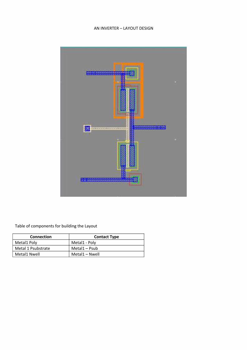
AN INVERTER – LAYOUT DESIGN
Table of components for building the Layout
Connection Contact TypeMetal1 Poly Metal1 - PolyMetal 1 Psubstrate Metal1 – PsubMetal1 Nwell Metal1 – Nwell
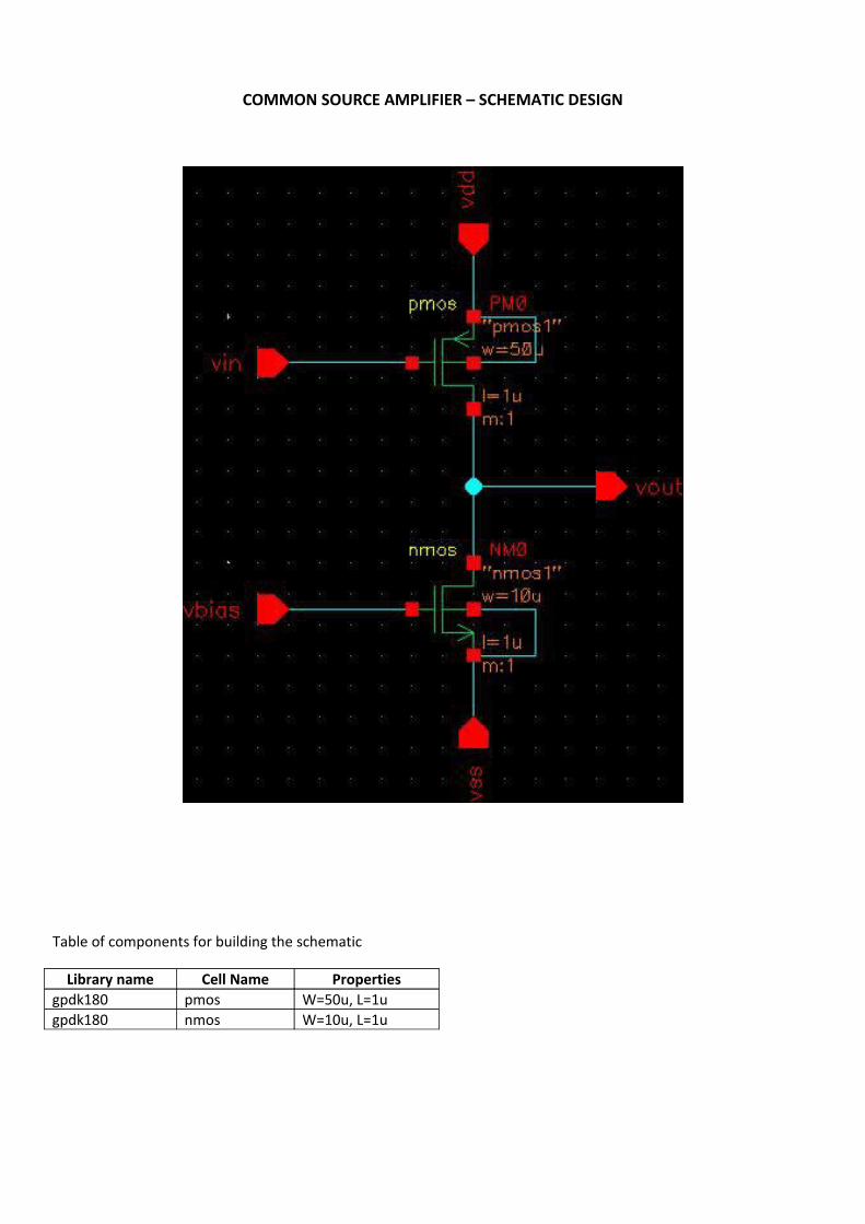
COMMON SOURCE AMPLIFIER – SCHEMATIC DESIGN
Table of components for building the schematic
Library name Cell Name Propertiesgpdk180 pmos W=50u, L=1ugpdk180 nmos W=10u, L=1u
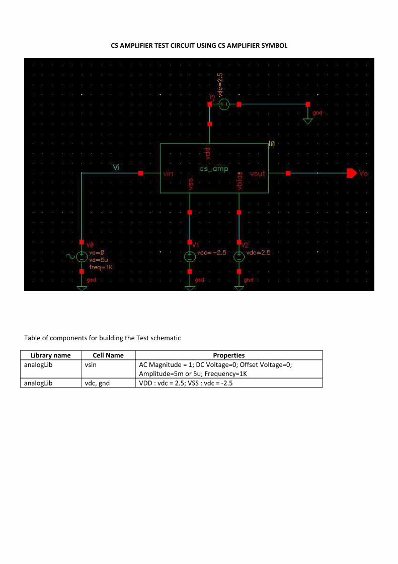
CS AMPLIFIER TEST CIRCUIT USING CS AMPLIFIER SYMBOL
Table of components for building the Test schematic
Library name Cell Name PropertiesanalogLib vsin AC Magnitude = 1; DC Voltage=0; Offset Voltage=0;
Amplitude=5m or 5u; Frequency=1KanalogLib vdc, gnd VDD : vdc = 2.5; VSS : vdc = -2.5
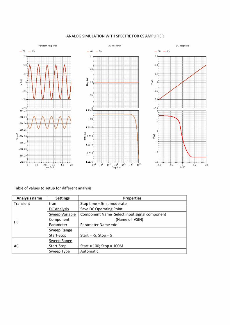
ANALOG SIMULATION WITH SPECTRE FOR CS AMPLIFIER
Table of values to setup for different analysis
Analysis name Settings PropertiesTransient tran Stop time = 5m , moderate
DC
DC Analysis Save DC Operating PointSweep VariableComponent Parameter
Component Name=Select input signal component (Name of VSIN)Parameter Name =dc
Sweep RangeStart-Stop Start = -5, Stop = 5
ACSweep RangeStart-Stop Start = 100; Stop = 100MSweep Type Automatic
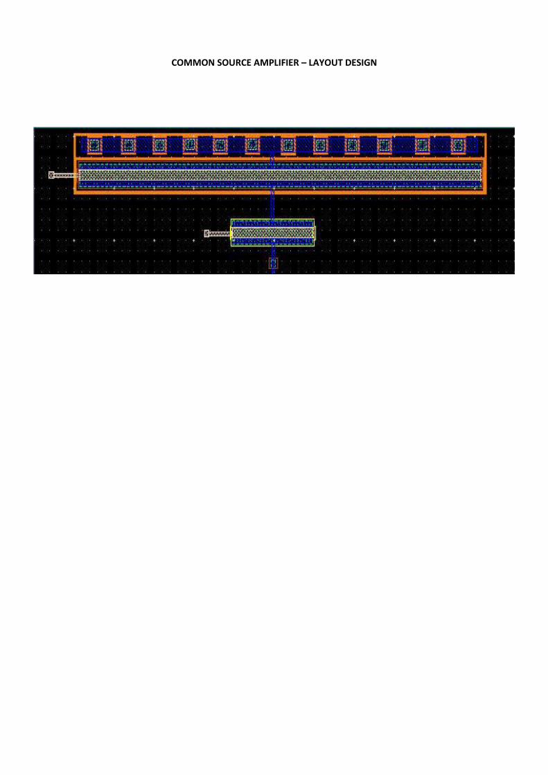
COMMON SOURCE AMPLIFIER – LAYOUT DESIGN
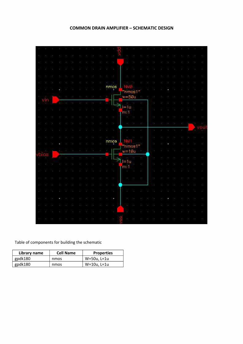
COMMON DRAIN AMPLIFIER – SCHEMATIC DESIGN
Table of components for building the schematic
Library name Cell Name Propertiesgpdk180 nmos W=50u, L=1ugpdk180 nmos W=10u, L=1u
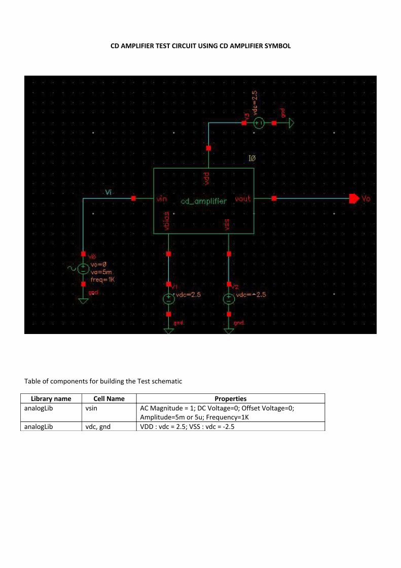
CD AMPLIFIER TEST CIRCUIT USING CD AMPLIFIER SYMBOL
Table of components for building the Test schematic
Library name Cell Name PropertiesanalogLib vsin AC Magnitude = 1; DC Voltage=0; Offset Voltage=0;
Amplitude=5m or 5u; Frequency=1KanalogLib vdc, gnd VDD : vdc = 2.5; VSS : vdc = -2.5
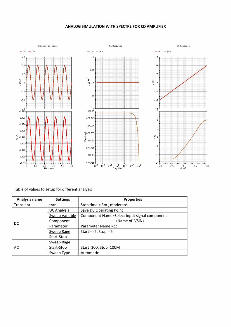
ANALOG SIMULATION WITH SPECTRE FOR CD AMPLIFIER
Table of values to setup for different analysis
Analysis name Settings PropertiesTransient tran Stop time = 5m , moderate
DC
DC Analysis Save DC Operating PointSweep VariableComponent Parameter
Component Name=Select input signal component (Name of VSIN)Parameter Name =dc
Sweep RageStart-Stop
Start = -5, Stop = 5
ACSweep RageStart-Stop Start=100; Stop=100MSweep Type Automatic
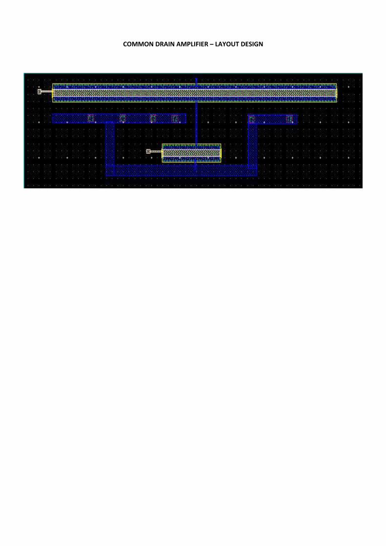
COMMON DRAIN AMPLIFIER – LAYOUT DESIGN
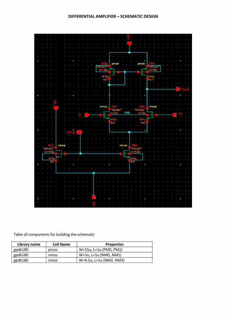
DIFFERENTIAL AMPLIFIER – SCHEMATIC DESIGN
Table of components for building the schematic
Library name Cell Name Propertiesgpdk180 pmos W=15u, L=1u (PM0, PM1)gpdk180 nmos W=3u, L=1u (NM0, NM1)gpdk180 nmos W=4.5u, L=1u (NM2, NM3)
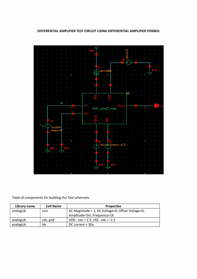
DIFFERENTIAL AMPLIFIER TEST CIRCUIT USING DIFFERENTIAL AMPLIFIER SYMBOL
Table of components for building the Test schematic
Library name Cell Name PropertiesanalogLib vsin AC Magnitude = 1; DC Voltage=0; Offset Voltage=0;
Amplitude=5m; Frequency=1KanalogLib vdc, gnd VDD : vdc = 2.5; VSS : vdc = -2.5analogLib Idc DC current = 30u
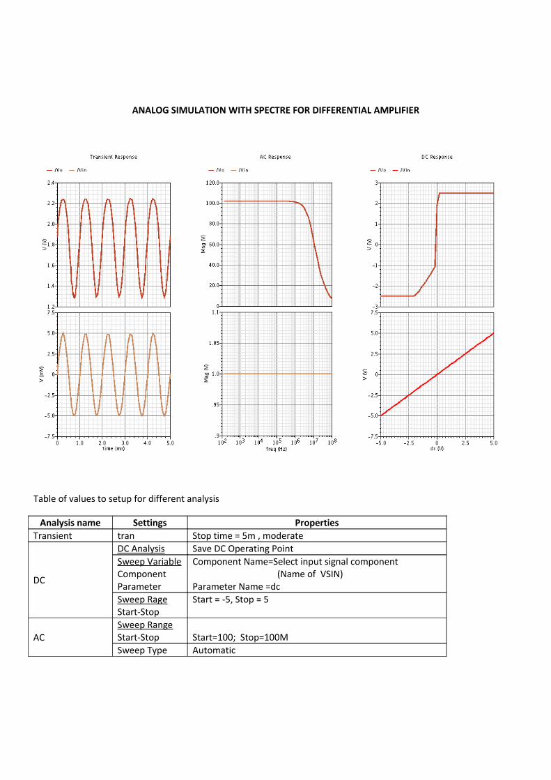
ANALOG SIMULATION WITH SPECTRE FOR DIFFERENTIAL AMPLIFIER
Table of values to setup for different analysis
Analysis name Settings PropertiesTransient tran Stop time = 5m , moderate
DC
DC Analysis Save DC Operating PointSweep VariableComponent Parameter
Component Name=Select input signal component (Name of VSIN)Parameter Name =dc
Sweep RageStart-Stop
Start = -5, Stop = 5
ACSweep RangeStart-Stop Start=100; Stop=100MSweep Type Automatic
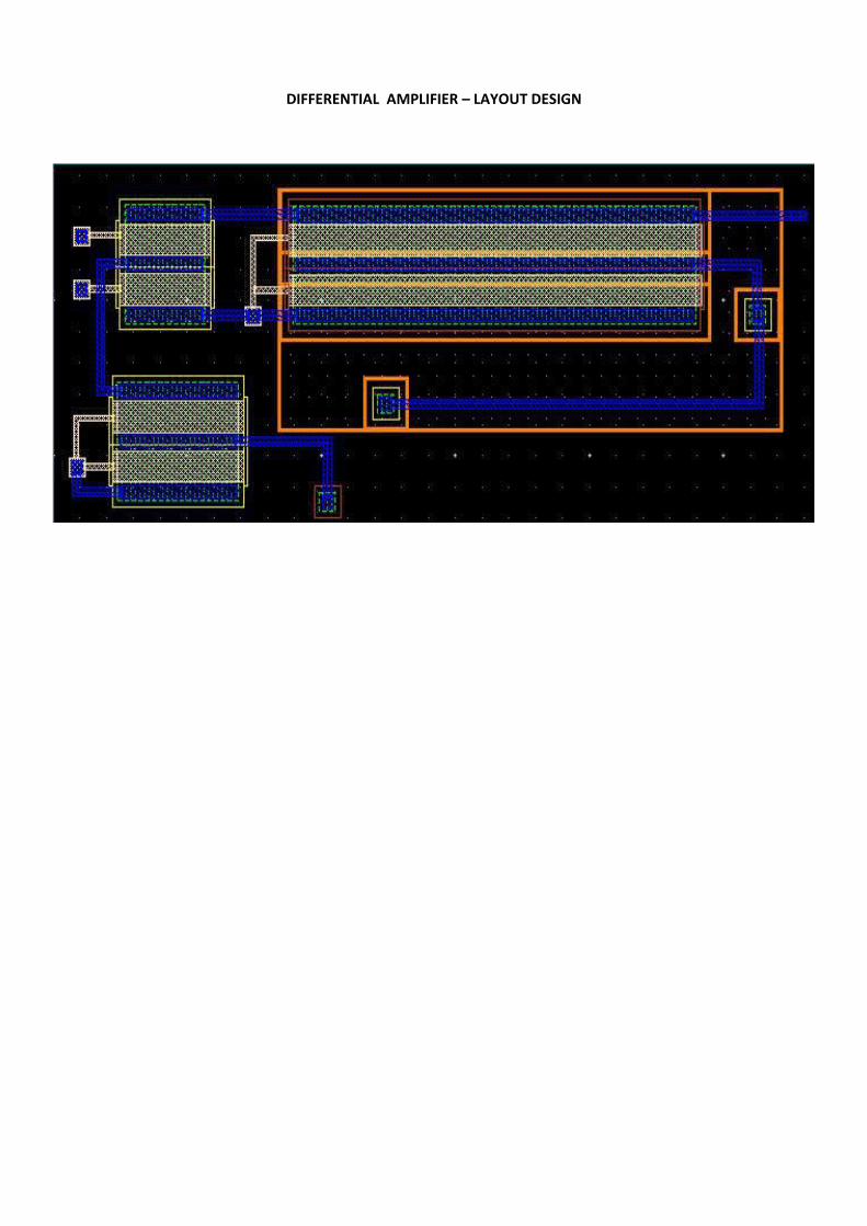
DIFFERENTIAL AMPLIFIER – LAYOUT DESIGN
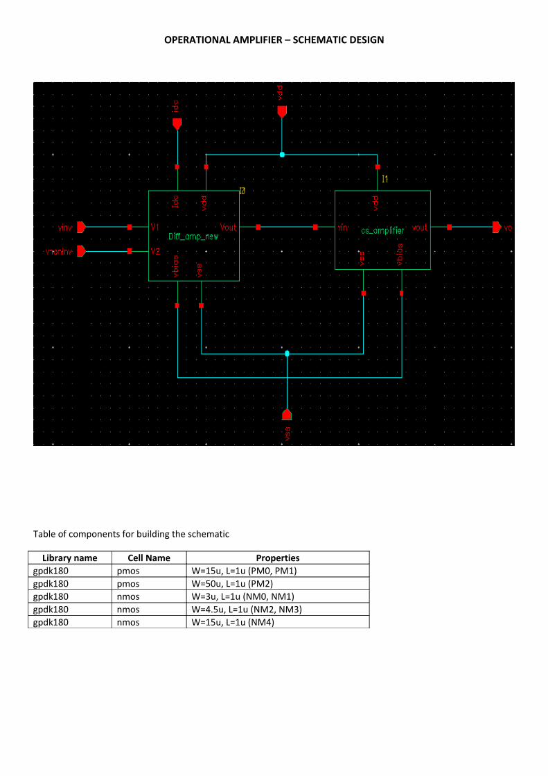
OPERATIONAL AMPLIFIER – SCHEMATIC DESIGN
Table of components for building the schematic
Library name Cell Name Propertiesgpdk180 pmos W=15u, L=1u (PM0, PM1)gpdk180 pmos W=50u, L=1u (PM2)gpdk180 nmos W=3u, L=1u (NM0, NM1)gpdk180 nmos W=4.5u, L=1u (NM2, NM3)gpdk180 nmos W=15u, L=1u (NM4)
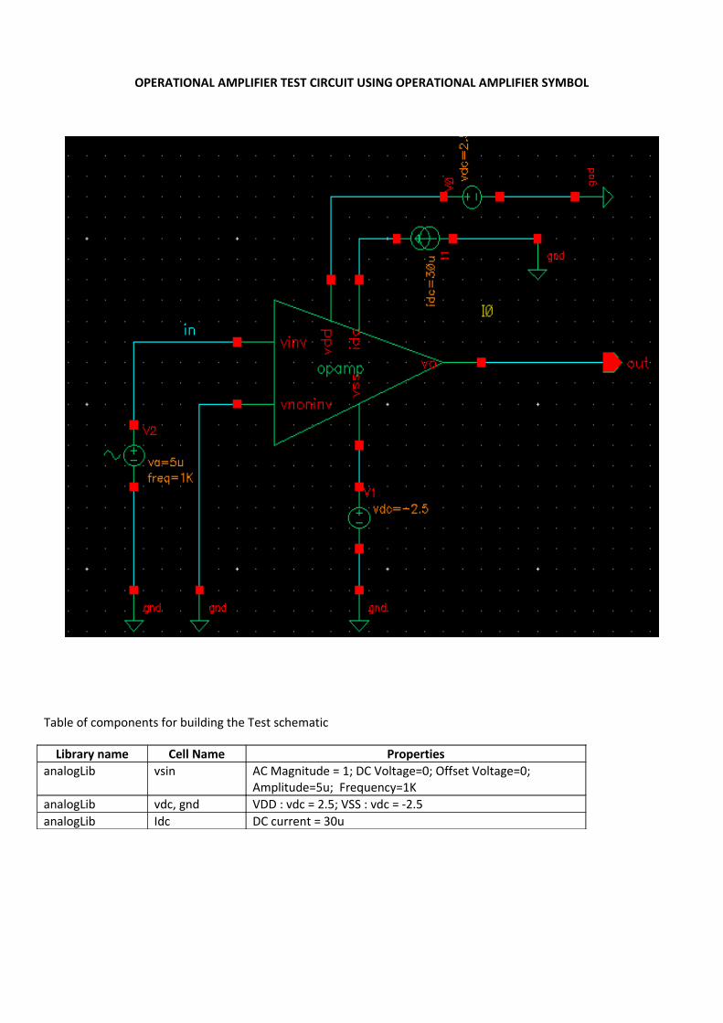
OPERATIONAL AMPLIFIER TEST CIRCUIT USING OPERATIONAL AMPLIFIER SYMBOL
Table of components for building the Test schematic
Library name Cell Name PropertiesanalogLib vsin AC Magnitude = 1; DC Voltage=0; Offset Voltage=0;
Amplitude=5u; Frequency=1KanalogLib vdc, gnd VDD : vdc = 2.5; VSS : vdc = -2.5analogLib Idc DC current = 30u
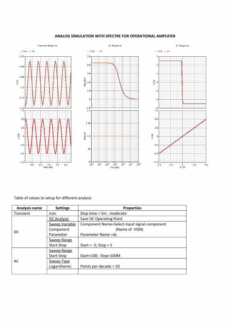
ANALOG SIMULATION WITH SPECTRE FOR OPERATIONAL AMPLIFIER
Table of values to setup for different analysis
Analysis name Settings PropertiesTransient tran Stop time = 5m , moderate
DC
DC Analysis Save DC Operating PointSweep VariableComponent Parameter
Component Name=Select input signal component (Name of VSIN)Parameter Name =dc
Sweep RangeStart-Stop Start = -5; Stop = 5
AC
Sweep RangeStart-Stop Start=100; Stop=100MSweep TypeLogarithemic Points per decade = 20
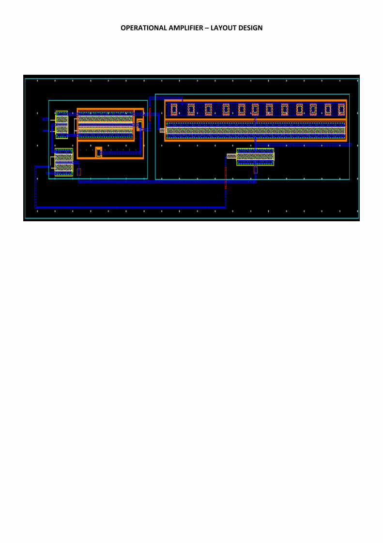
OPERATIONAL AMPLIFIER – LAYOUT DESIGN
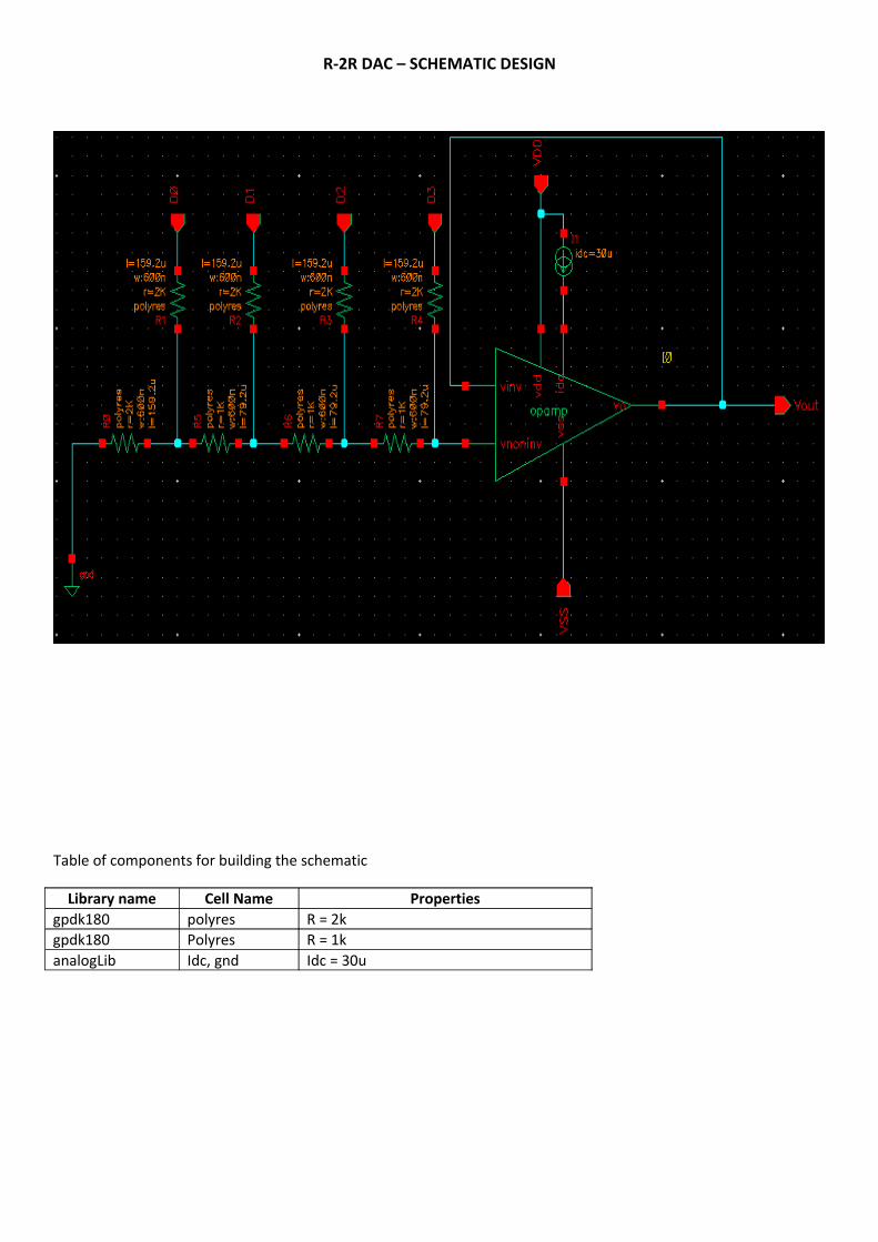
R-2R DAC – SCHEMATIC DESIGN
Table of components for building the schematic
Library name Cell Name Propertiesgpdk180 polyres R = 2kgpdk180 Polyres R = 1kanalogLib Idc, gnd Idc = 30u
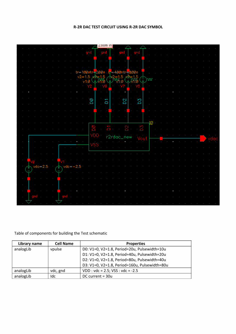
R-2R DAC TEST CIRCUIT USING R-2R DAC SYMBOL
Table of components for building the Test schematic
Library name Cell Name PropertiesanalogLib vpulse D0: V1=0, V2=1.8, Period=20u, Pulsewidth=10u
D1: V1=0, V2=1.8, Period=40u, Pulsewidth=20uD2: V1=0, V2=1.8, Period=80u, Pulsewidth=40uD3: V1=0, V2=1.8, Period=160u, Pulsewidth=80u
analogLib vdc, gnd VDD : vdc = 2.5; VSS : vdc = -2.5analogLib Idc DC current = 30u
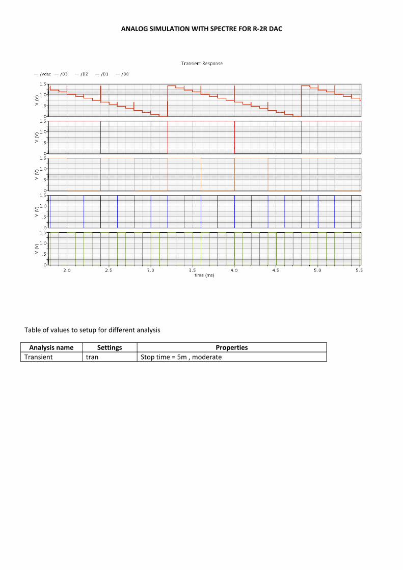
ANALOG SIMULATION WITH SPECTRE FOR R-2R DAC
Table of values to setup for different analysis
Analysis name Settings PropertiesTransient tran Stop time = 5m , moderate
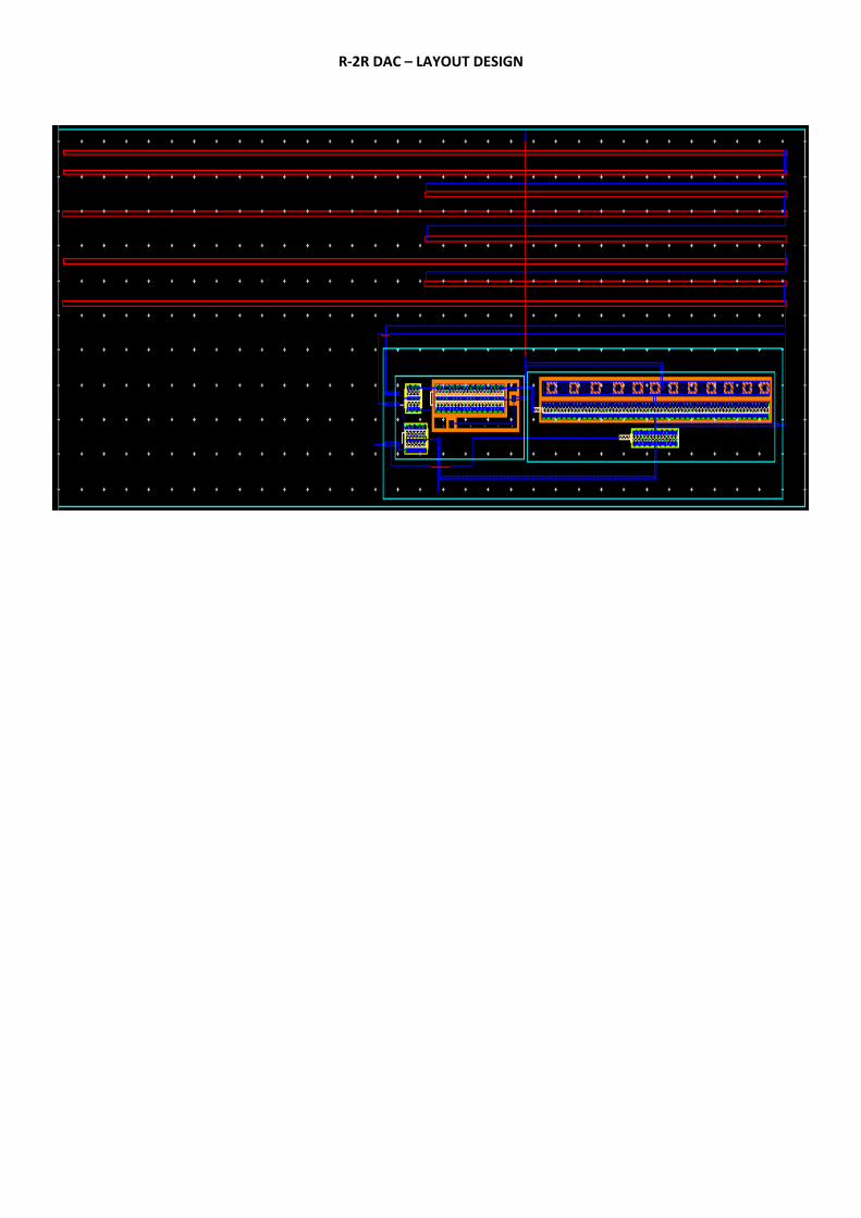
R-2R DAC – LAYOUT DESIGN
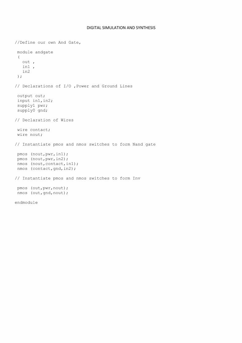
DIGITAL SIMULATION AND SYNTHESIS
//Define our own And Gate,
module andgate ( out , in1 , in2 );
// Declarations of I/O ,Power and Ground Lines
output out; input in1,in2; supply1 pwr; supply0 gnd;
// Declaration of Wires
wire contact; wire nout;
// Instantiate pmos and nmos switches to form Nand gate pmos (nout,pwr,in1); pmos (nout,pwr,in2); nmos (nout,contact,in1); nmos (contact,gnd,in2); // Instantiate pmos and nmos switches to form Inv
pmos (out,pwr,nout); nmos (out,gnd,nout);
endmodule
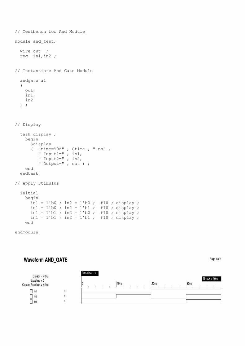
// Testbench for And Module
module and_test;
wire out ; reg in1,in2 ;
// Instantiate And Gate Module
andgate a1 ( out, in1, in2 ) ;
// Display
task display ; begin $display ( "time=%0d" , $time , " ns" , " Input1=" , in1, " Input2=" , in2, " Output=" , out ) ; end endtask
// Apply Stimulus
initial begin in1 = 1'b0 ; in2 = 1'b0 ; #10 ; display ; in1 = 1'b0 ; in2 = 1'b1 ; #10 ; display ; in1 = 1'b1 ; in2 = 1'b0 ; #10 ; display ; in1 = 1'b1 ; in2 = 1'b1 ; #10 ; display ; end
endmodule
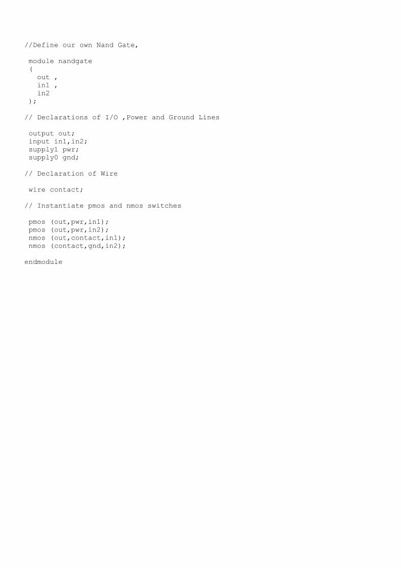
//Define our own Nand Gate,
module nandgate ( out , in1 , in2 );
// Declarations of I/O ,Power and Ground Lines
output out; input in1,in2; supply1 pwr; supply0 gnd;
// Declaration of Wire
wire contact;
// Instantiate pmos and nmos switches pmos (out,pwr,in1); pmos (out,pwr,in2); nmos (out,contact,in1); nmos (contact,gnd,in2); endmodule
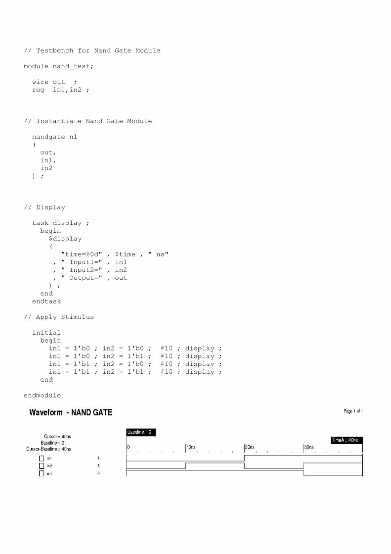
// Testbench for Nand Gate Module
module nand_test;
wire out ; reg in1,in2 ;
// Instantiate Nand Gate Module
nandgate n1 ( out, in1, in2 ) ;
// Display
task display ; begin $display ( "time=%0d" , $time , " ns" , " Input1=" , in1 , " Input2=" , in2 , " Output=" , out ) ; end endtask
// Apply Stimulus
initial begin in1 = 1'b0 ; in2 = 1'b0 ; #10 ; display ; in1 = 1'b0 ; in2 = 1'b1 ; #10 ; display ; in1 = 1'b1 ; in2 = 1'b0 ; #10 ; display ; in1 = 1'b1 ; in2 = 1'b1 ; #10 ; display ; end
endmodule
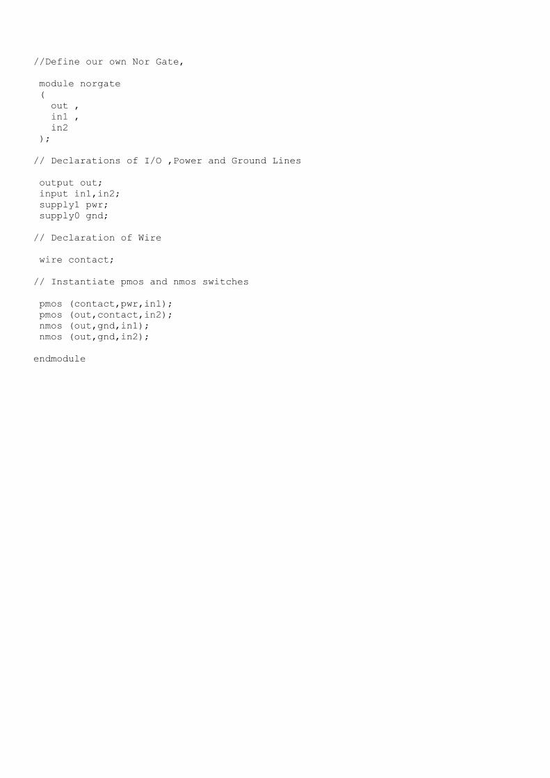
//Define our own Nor Gate,
module norgate ( out , in1 , in2 );
// Declarations of I/O ,Power and Ground Lines
output out; input in1,in2; supply1 pwr; supply0 gnd;
// Declaration of Wire
wire contact;
// Instantiate pmos and nmos switches pmos (contact,pwr,in1); pmos (out,contact,in2); nmos (out,gnd,in1); nmos (out,gnd,in2); endmodule
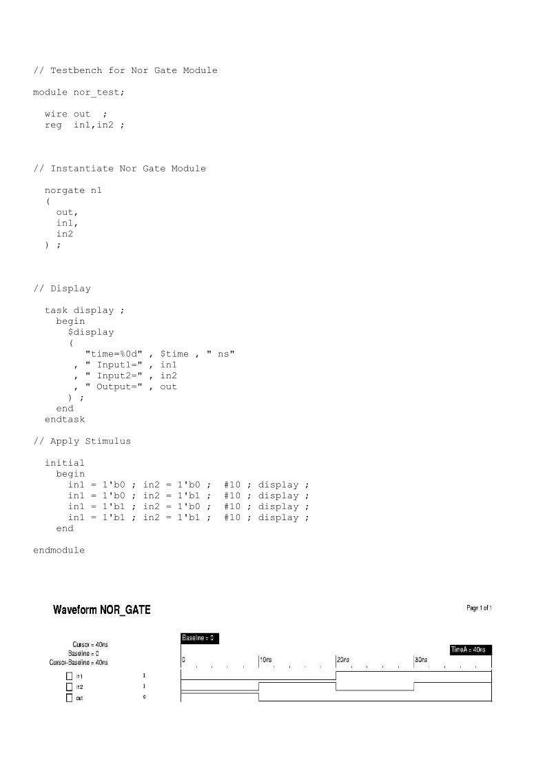
// Testbench for Nor Gate Module
module nor_test;
wire out ; reg in1,in2 ;
// Instantiate Nor Gate Module
norgate n1 ( out, in1, in2 ) ;
// Display
task display ; begin $display ( "time=%0d" , $time , " ns" , " Input1=" , in1 , " Input2=" , in2 , " Output=" , out ) ; end endtask
// Apply Stimulus
initial begin in1 = 1'b0 ; in2 = 1'b0 ; #10 ; display ; in1 = 1'b0 ; in2 = 1'b1 ; #10 ; display ; in1 = 1'b1 ; in2 = 1'b0 ; #10 ; display ; in1 = 1'b1 ; in2 = 1'b1 ; #10 ; display ; end
endmodule
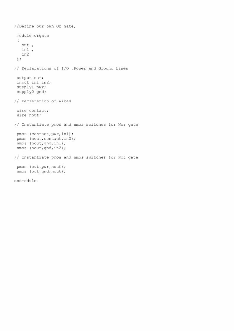
//Define our own Or Gate,
module orgate ( out , in1 , in2 );
// Declarations of I/O ,Power and Ground Lines
output out; input in1,in2; supply1 pwr; supply0 gnd;
// Declaration of Wires
wire contact; wire nout;
// Instantiate pmos and nmos switches for Nor gate pmos (contact,pwr,in1); pmos (nout,contact,in2); nmos (nout,gnd,in1); nmos (nout,gnd,in2); // Instantiate pmos and nmos switches for Not gate
pmos (out,pwr,nout); nmos (out,gnd,nout); endmodule
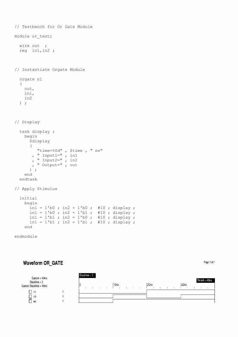
// Testbench for Or Gate Module
module or_test;
wire out ; reg in1,in2 ;
// Instantiate Orgate Module
orgate n1 ( out, in1, in2 ) ;
// Display
task display ; begin $display ( "time=%0d" , $time , " ns" , " Input1=" , in1 , " Input2=" , in2 , " Output=" , out ) ; end endtask
// Apply Stimulus
initial begin in1 = 1'b0 ; in2 = 1'b0 ; #10 ; display ; in1 = 1'b0 ; in2 = 1'b1 ; #10 ; display ; in1 = 1'b1 ; in2 = 1'b0 ; #10 ; display ; in1 = 1'b1 ; in2 = 1'b1 ; #10 ; display ; end
endmodule
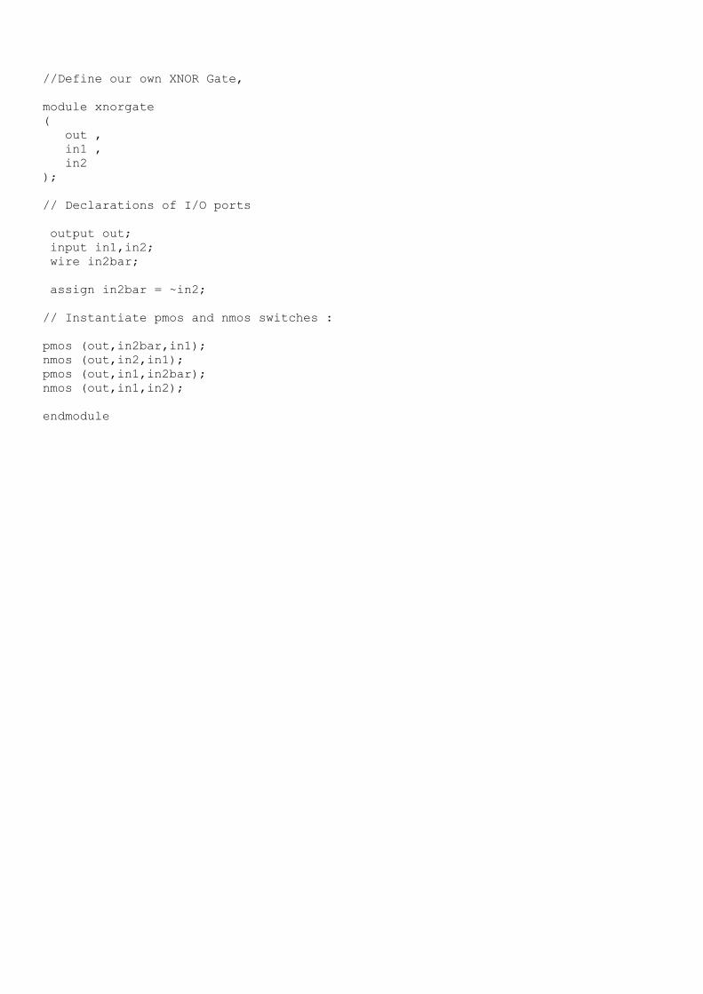
//Define our own XNOR Gate,
module xnorgate( out , in1 , in2 );
// Declarations of I/O ports
output out; input in1,in2; wire in2bar;
assign in2bar = ~in2;
// Instantiate pmos and nmos switches :
pmos (out,in2bar,in1);nmos (out,in2,in1);pmos (out,in1,in2bar);nmos (out,in1,in2);
endmodule
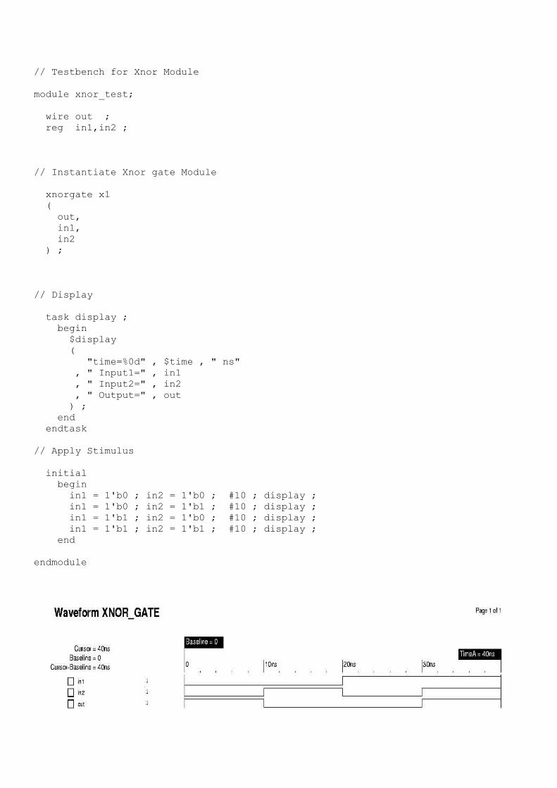
// Testbench for Xnor Module
module xnor_test;
wire out ; reg in1,in2 ;
// Instantiate Xnor gate Module
xnorgate x1 ( out, in1, in2 ) ;
// Display
task display ; begin $display ( "time=%0d" , $time , " ns" , " Input1=" , in1 , " Input2=" , in2 , " Output=" , out ) ; end endtask
// Apply Stimulus
initial begin in1 = 1'b0 ; in2 = 1'b0 ; #10 ; display ; in1 = 1'b0 ; in2 = 1'b1 ; #10 ; display ; in1 = 1'b1 ; in2 = 1'b0 ; #10 ; display ; in1 = 1'b1 ; in2 = 1'b1 ; #10 ; display ; end
endmodule
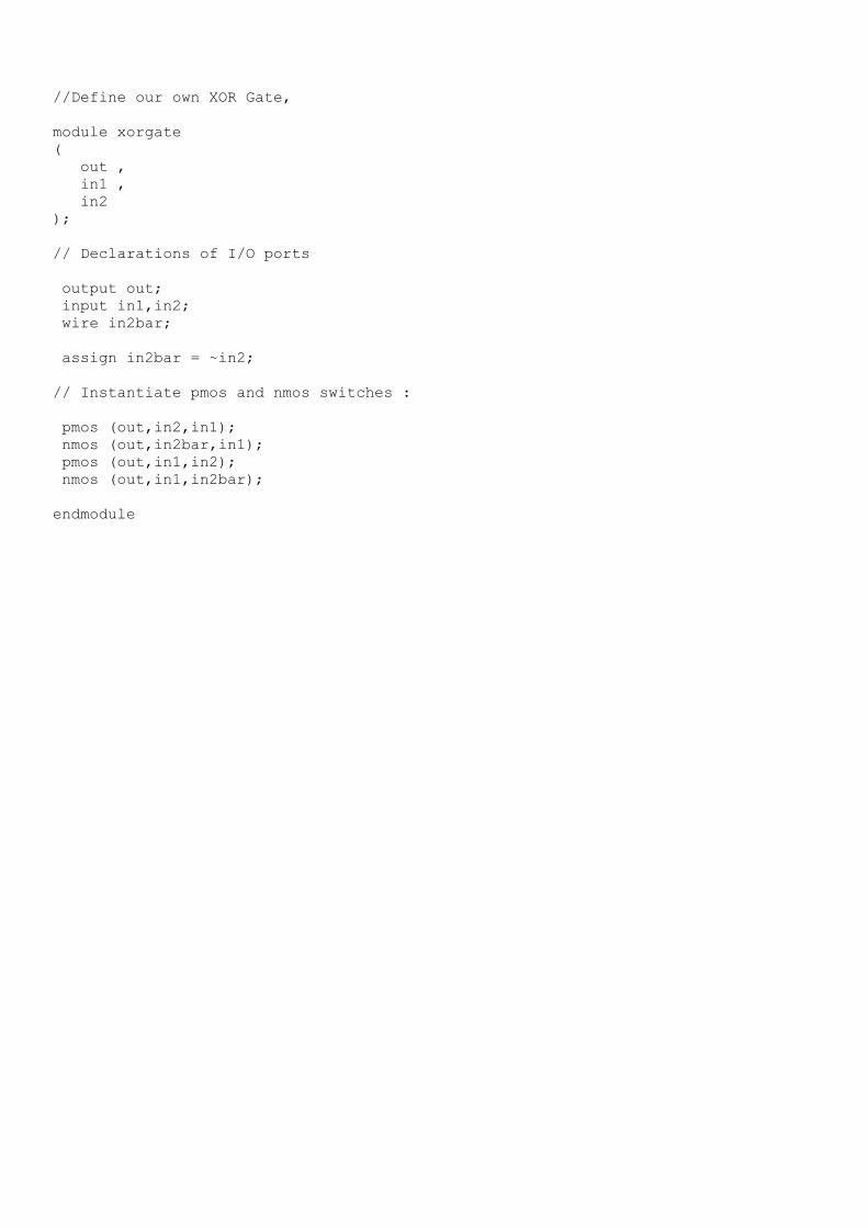
//Define our own XOR Gate,
module xorgate( out , in1 , in2 );
// Declarations of I/O ports
output out; input in1,in2; wire in2bar;
assign in2bar = ~in2;
// Instantiate pmos and nmos switches :
pmos (out,in2,in1); nmos (out,in2bar,in1); pmos (out,in1,in2); nmos (out,in1,in2bar);
endmodule
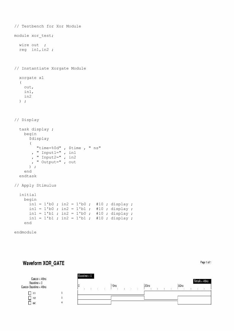
// Testbench for Xor Module
module xor_test;
wire out ; reg in1,in2 ;
// Instantiate Xorgate Module
xorgate x1 ( out, in1, in2 ) ;
// Display
task display ; begin $display ( "time=%0d" , $time , " ns" , " Input1=" , in1 , " Input2=" , in2 , " Output=" , out ) ; end endtask
// Apply Stimulus
initial begin in1 = 1'b0 ; in2 = 1'b0 ; #10 ; display ; in1 = 1'b0 ; in2 = 1'b1 ; #10 ; display ; in1 = 1'b1 ; in2 = 1'b0 ; #10 ; display ; in1 = 1'b1 ; in2 = 1'b1 ; #10 ; display ; end
endmodule
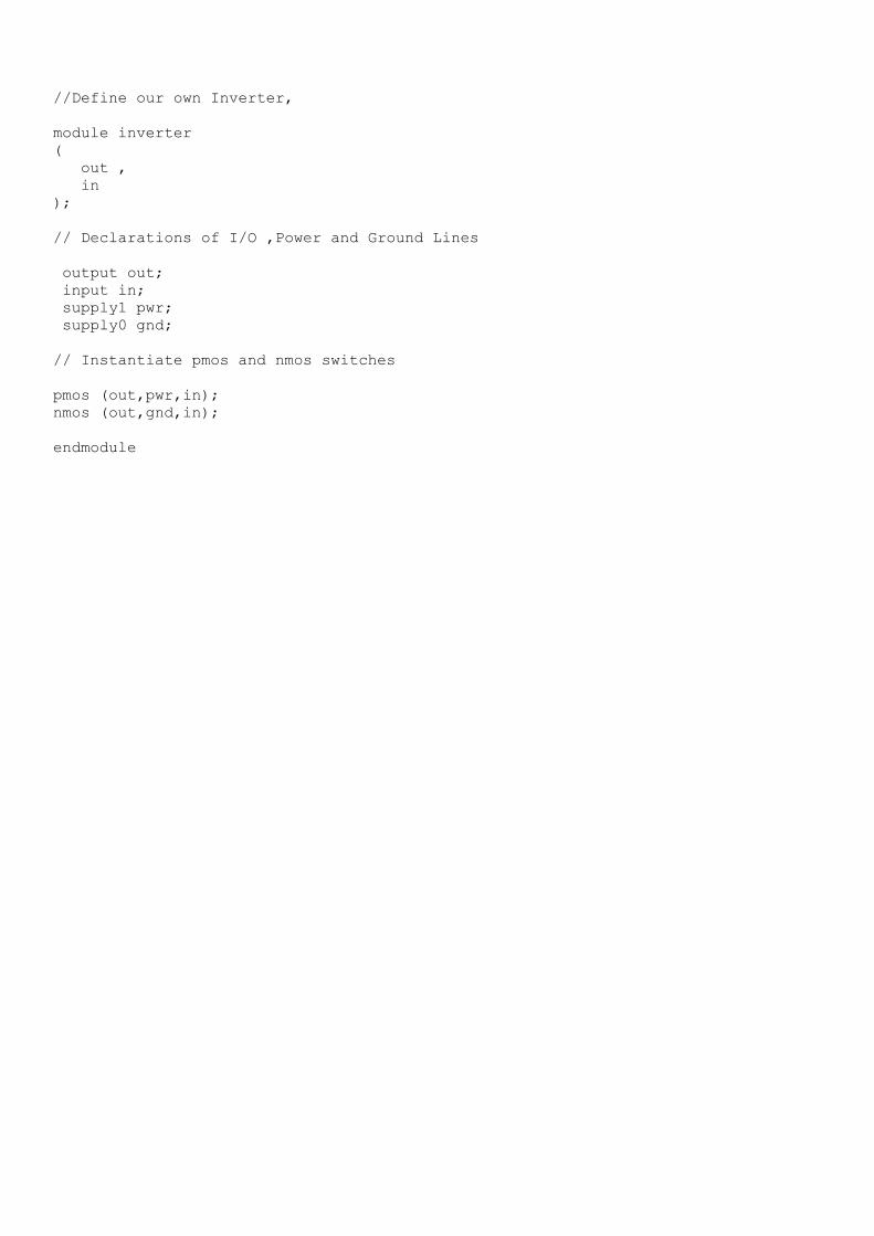
//Define our own Inverter,
module inverter( out , in );
// Declarations of I/O ,Power and Ground Lines
output out; input in; supply1 pwr; supply0 gnd;
// Instantiate pmos and nmos switches pmos (out,pwr,in);nmos (out,gnd,in); endmodule
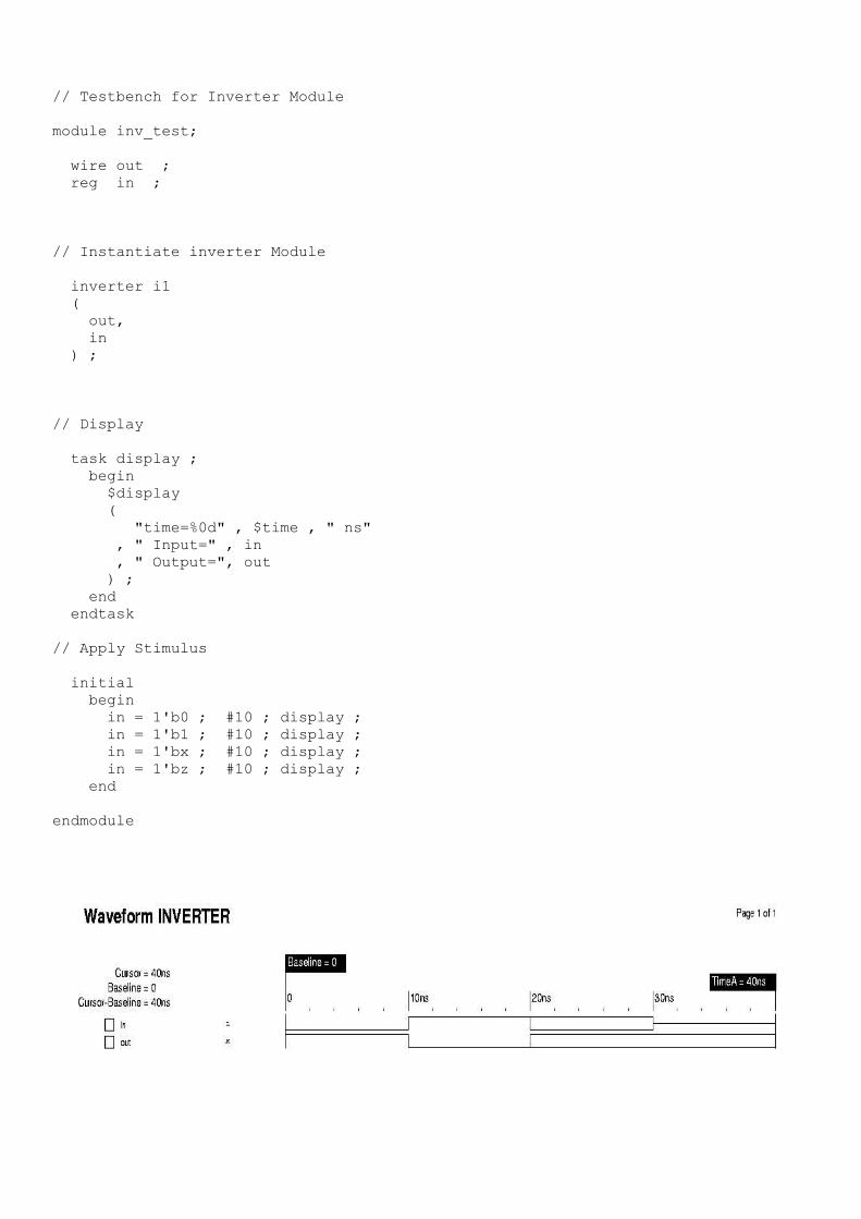
// Testbench for Inverter Module
module inv_test;
wire out ; reg in ;
// Instantiate inverter Module
inverter i1 ( out, in ) ;
// Display
task display ; begin $display ( "time=%0d" , $time , " ns" , " Input=" , in , " Output=", out ) ; end endtask
// Apply Stimulus
initial begin in = 1'b0 ; #10 ; display ; in = 1'b1 ; #10 ; display ; in = 1'bx ; #10 ; display ; in = 1'bz ; #10 ; display ; end
endmodule
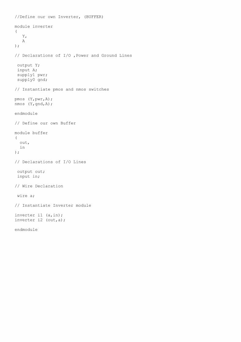
//Define our own Inverter, (BUFFER)
module inverter( Y, A );
// Declarations of I/O ,Power and Ground Lines
output Y; input A; supply1 pwr; supply0 gnd;
// Instantiate pmos and nmos switches pmos (Y,pwr,A);nmos (Y,gnd,A); endmodule
// Define our own Buffer
module buffer( out, in);
// Declarations of I/O Lines
output out; input in;
// Wire Declaration
wire a;
// Instantiate Inverter module
inverter i1 (a,in);inverter i2 (out,a);
endmodule
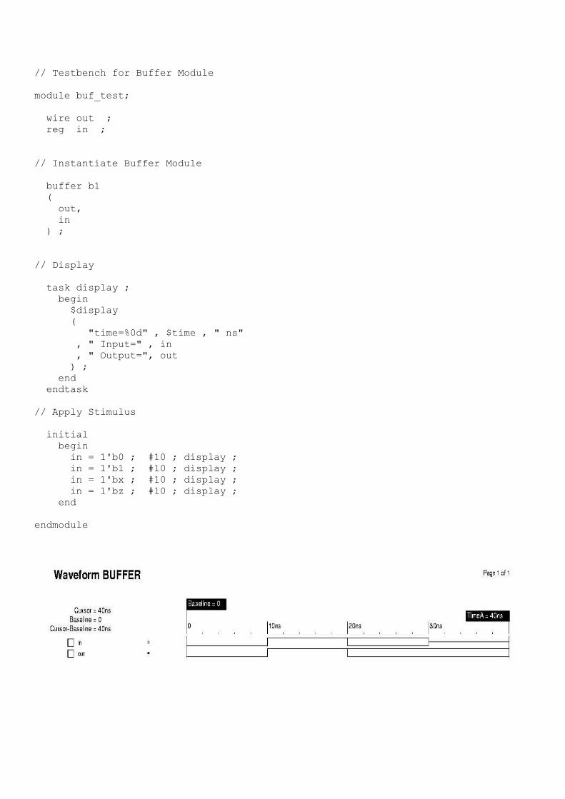
// Testbench for Buffer Module
module buf_test;
wire out ; reg in ;
// Instantiate Buffer Module
buffer b1 ( out, in ) ;
// Display
task display ; begin $display ( "time=%0d" , $time , " ns" , " Input=" , in , " Output=", out ) ; end endtask
// Apply Stimulus
initial begin in = 1'b0 ; #10 ; display ; in = 1'b1 ; #10 ; display ; in = 1'bx ; #10 ; display ; in = 1'bz ; #10 ; display ; end
endmodule
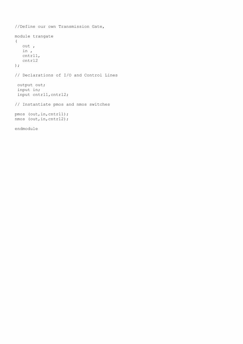
//Define our own Transmission Gate,
module trangate( out , in , cntrl1, cntrl2);
// Declarations of I/O and Control Lines
output out; input in; input cntrl1,cntrl2;
// Instantiate pmos and nmos switches
pmos (out,in,cntrl1);nmos (out,in,cntrl2);
endmodule
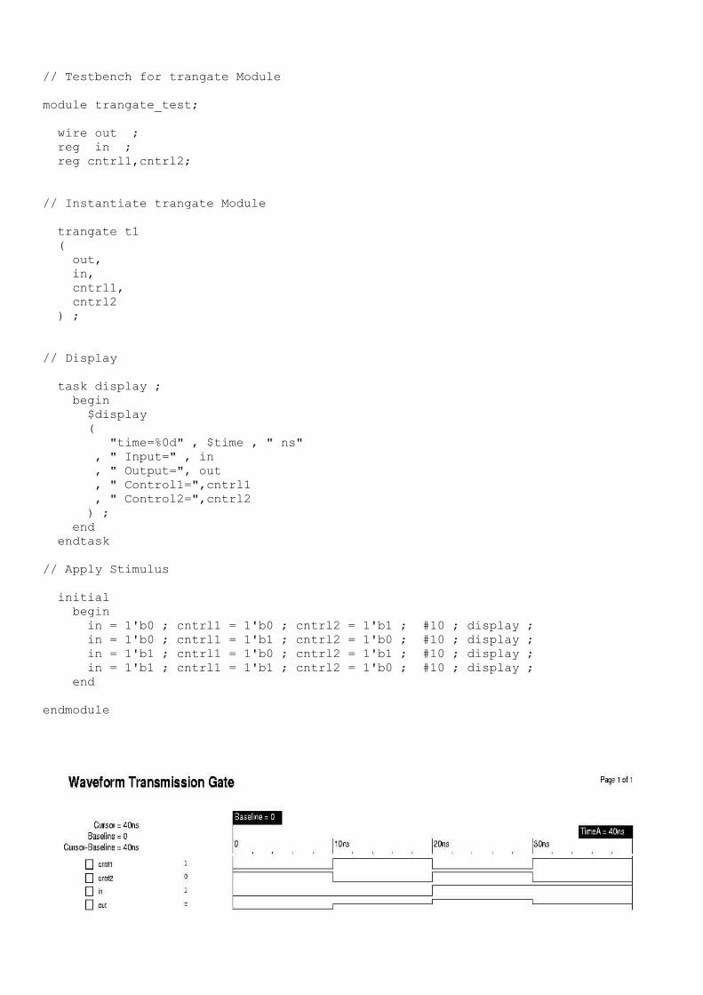
// Testbench for trangate Module
module trangate_test;
wire out ; reg in ; reg cntrl1,cntrl2;
// Instantiate trangate Module
trangate t1 ( out, in, cntrl1, cntrl2 ) ;
// Display
task display ; begin $display ( "time=%0d" , $time , " ns" , " Input=" , in , " Output=", out , " Control1=",cntrl1 , " Control2=",cntrl2 ) ; end endtask
// Apply Stimulus
initial begin in = 1'b0 ; cntrl1 = 1'b0 ; cntrl2 = 1'b1 ; #10 ; display ; in = 1'b0 ; cntrl1 = 1'b1 ; cntrl2 = 1'b0 ; #10 ; display ; in = 1'b1 ; cntrl1 = 1'b0 ; cntrl2 = 1'b1 ; #10 ; display ; in = 1'b1 ; cntrl1 = 1'b1 ; cntrl2 = 1'b0 ; #10 ; display ; end
endmodule
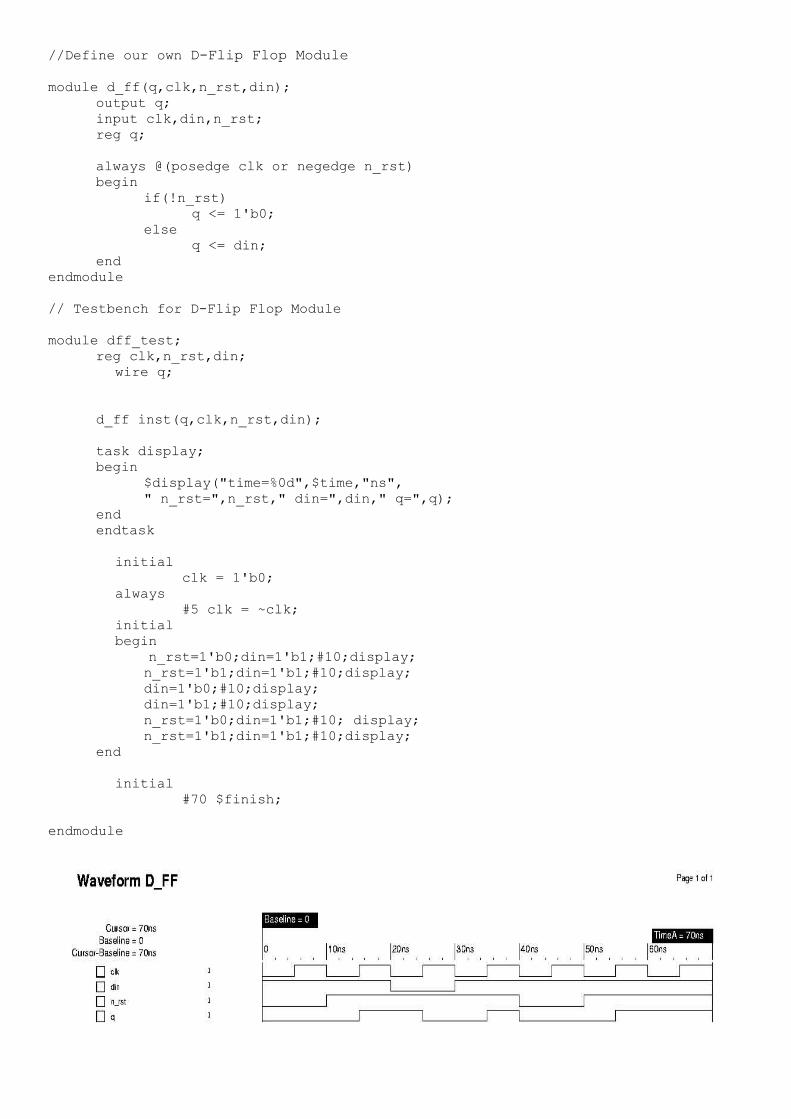
//Define our own D-Flip Flop Module
module d_ff(q,clk,n_rst,din);output q;input clk,din,n_rst;reg q;
always @(posedge clk or negedge n_rst)begin
if(!n_rst)q <= 1'b0;
elseq <= din;
endendmodule
// Testbench for D-Flip Flop Module
module dff_test;reg clk,n_rst,din;
wire q;
d_ff inst(q,clk,n_rst,din);
task display;begin
$display("time=%0d",$time,"ns"," n_rst=",n_rst," din=",din," q=",q);
endendtask
initial clk = 1'b0; always #5 clk = ~clk; initial begin n_rst=1'b0;din=1'b1;#10;display;
n_rst=1'b1;din=1'b1;#10;display;din=1'b0;#10;display;din=1'b1;#10;display;n_rst=1'b0;din=1'b1;#10; display;n_rst=1'b1;din=1'b1;#10;display;
end initial #70 $finish;
endmodule
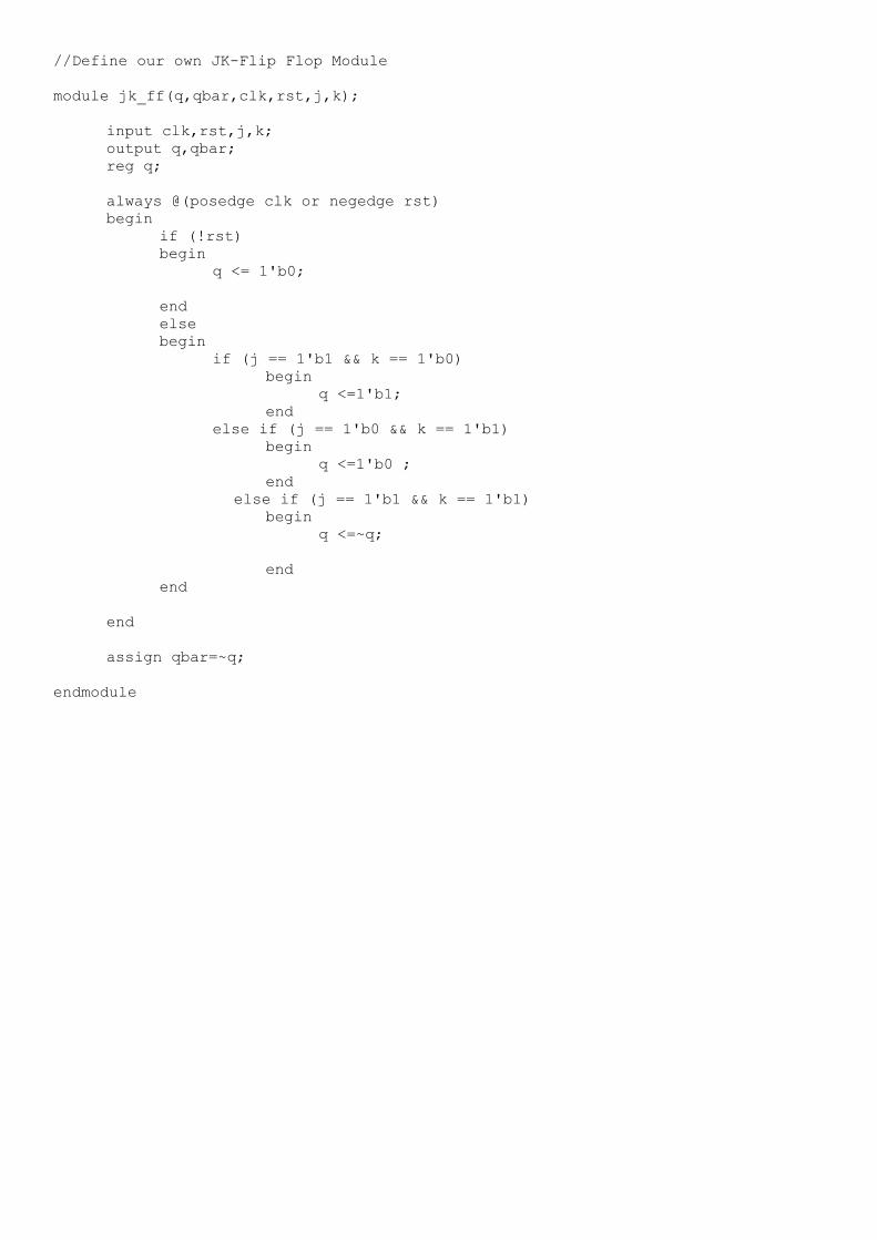
//Define our own JK-Flip Flop Module
module jk_ff(q,qbar,clk,rst,j,k);
input clk,rst,j,k;output q,qbar;reg q;
always @(posedge clk or negedge rst)begin
if (!rst)begin
q <= 1'b0;
endelsebegin
if (j == 1'b1 && k == 1'b0)begin
q <=1'b1;end
else if (j == 1'b0 && k == 1'b1)begin
q <=1'b0 ;end
else if (j == 1'b1 && k == 1'b1)begin
q <=~q;
endend
end
assign qbar=~q;
endmodule
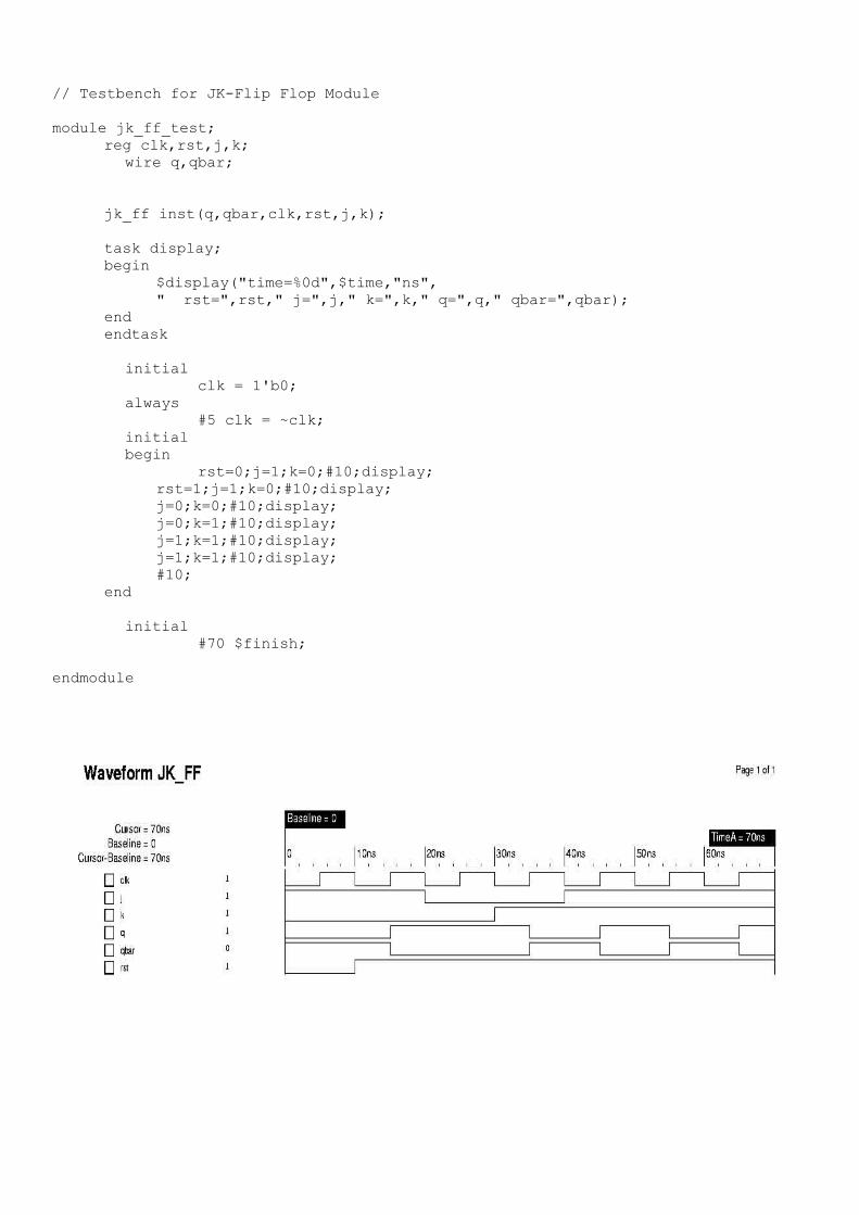
// Testbench for JK-Flip Flop Module
module jk_ff_test;reg clk,rst,j,k;
wire q,qbar;
jk_ff inst(q,qbar,clk,rst,j,k);
task display;begin
$display("time=%0d",$time,"ns"," rst=",rst," j=",j," k=",k," q=",q," qbar=",qbar);
endendtask
initial clk = 1'b0; always #5 clk = ~clk; initial begin rst=0;j=1;k=0;#10;display;
rst=1;j=1;k=0;#10;display;j=0;k=0;#10;display;j=0;k=1;#10;display;j=1;k=1;#10;display;j=1;k=1;#10;display;#10;
end initial #70 $finish;
endmodule
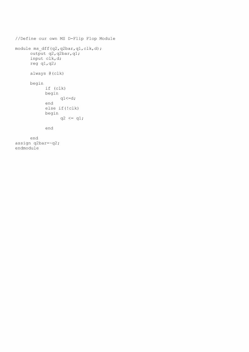
//Define our own MS D-Flip Flop Module
module ms_dff(q2,q2bar,q1,clk,d);output q2,q2bar,q1;input clk,d;reg q1,q2;
always @(clk)
beginif (clk)begin
q1<=d;endelse if(!clk)begin
q2 <= q1;
end
endassign q2bar=~q2;endmodule
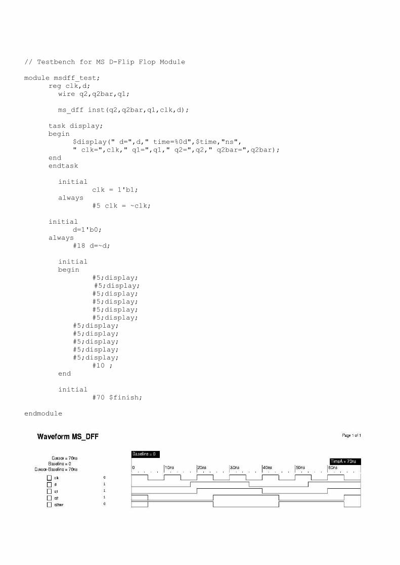
// Testbench for MS D-Flip Flop Module
module msdff_test;reg clk,d;
wire q2,q2bar,q1;
ms_dff inst(q2,q2bar,q1,clk,d);
task display;begin
$display(" d=",d," time=%0d",$time,"ns"," clk=",clk," q1=",q1," q2=",q2," q2bar=",q2bar);
endendtask
initial clk = 1'b1; always #5 clk = ~clk;
initiald=1'b0;
always#18 d=~d;
initial begin #5;display;
#5;display; #5;display; #5;display; #5;display; #5;display;
#5;display;#5;display;#5;display;#5;display;#5;display;
#10 ; end initial #70 $finish; endmodule
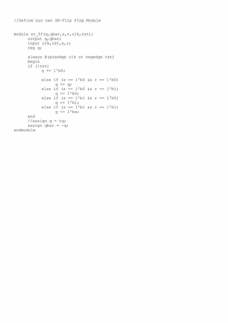
//Define our own SR-Flip Flop Module
module sr_ff(q,qbar,s,r,clk,rst);output q,qbar;input clk,rst,s,r;reg q;
always @(posedge clk or negedge rst)beginif (!rst)
q <= 1'b0;
else if (s == 1'b0 && r == 1'b0)q <= q;
else if (s == 1'b0 && r == 1'b1)q <= 1'b0;
else if (s == 1'b1 && r == 1'b0)q <= 1'b1;
else if (s == 1'b1 && r == 1'b1)q <= 1'bx;
end//assign q = tq;assign qbar = ~q;
endmodule
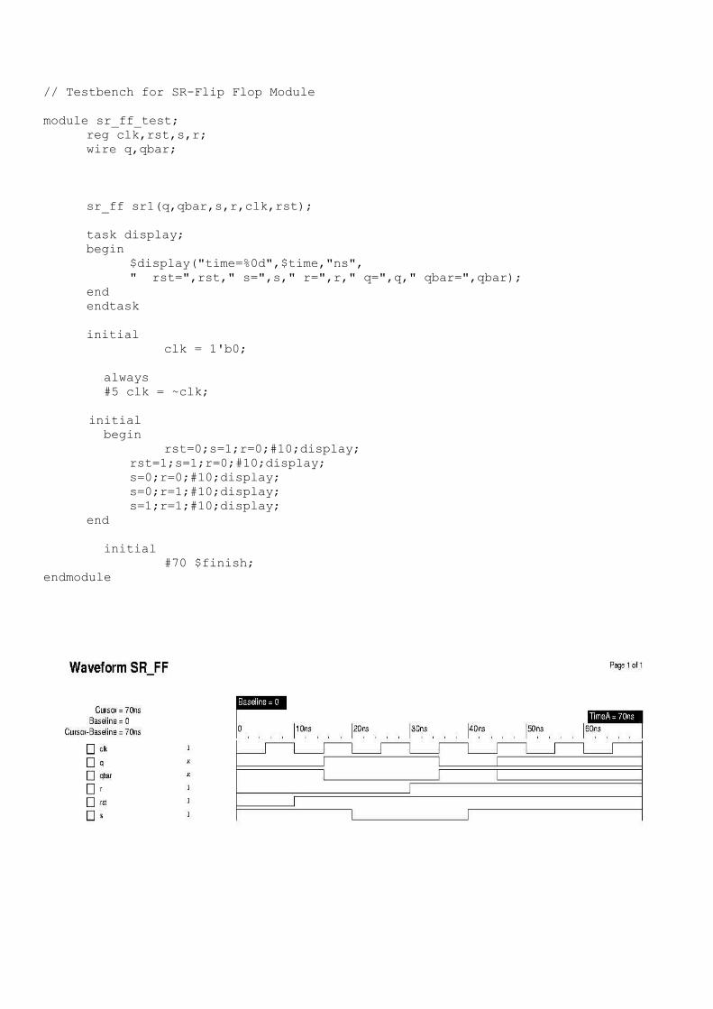
// Testbench for SR-Flip Flop Module
module sr_ff_test;reg clk,rst,s,r;wire q,qbar;
sr_ff sr1(q,qbar,s,r,clk,rst);
task display;begin
$display("time=%0d",$time,"ns"," rst=",rst," s=",s," r=",r," q=",q," qbar=",qbar);
endendtask
initial clk = 1'b0; always #5 clk = ~clk; initial begin rst=0;s=1;r=0;#10;display;
rst=1;s=1;r=0;#10;display;s=0;r=0;#10;display;s=0;r=1;#10;display;s=1;r=1;#10;display;
end initial #70 $finish;endmodule
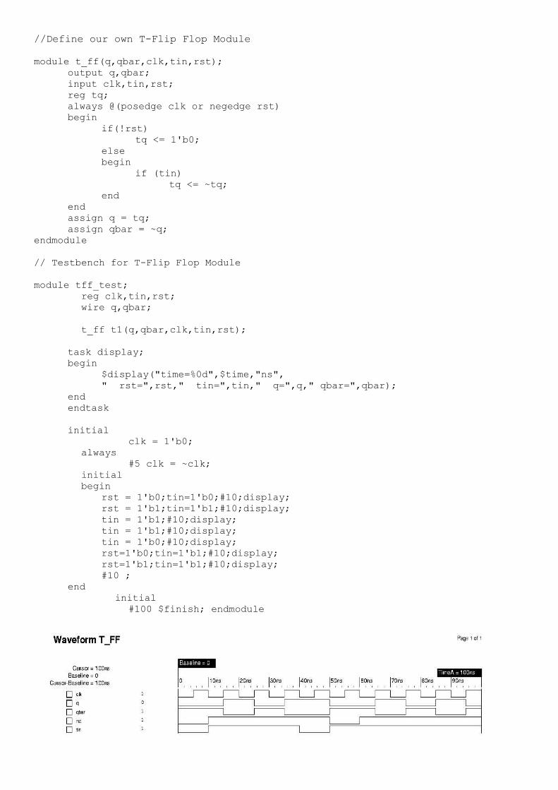
//Define our own T-Flip Flop Module
module t_ff(q,qbar,clk,tin,rst);output q,qbar;input clk,tin,rst;reg tq;always @(posedge clk or negedge rst)begin
if(!rst)tq <= 1'b0;
elsebegin
if (tin)tq <= ~tq;
endendassign q = tq;assign qbar = ~q;
endmodule
// Testbench for T-Flip Flop Module
module tff_test; reg clk,tin,rst; wire q,qbar;
t_ff t1(q,qbar,clk,tin,rst);
task display;begin
$display("time=%0d",$time,"ns"," rst=",rst," tin=",tin," q=",q," qbar=",qbar);
endendtask
initial clk = 1'b0; always #5 clk = ~clk; initial begin rst = 1'b0;tin=1'b0;#10;display;
rst = 1'b1;tin=1'b1;#10;display;tin = 1'b1;#10;display;tin = 1'b1;#10;display;tin = 1'b0;#10;display;rst=1'b0;tin=1'b1;#10;display;rst=1'b1;tin=1'b1;#10;display;#10 ;
end initial
#100 $finish; endmodule
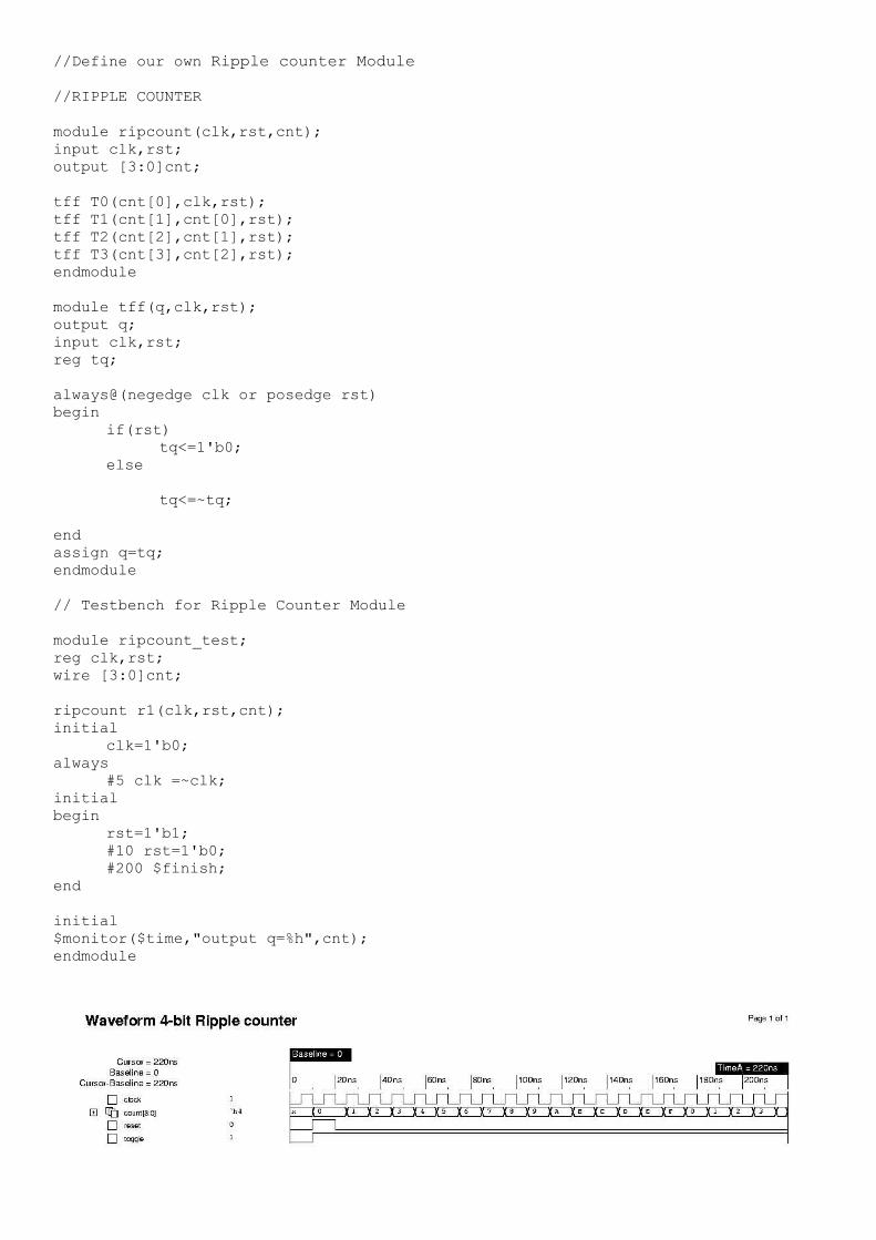
//Define our own Ripple counter Module
//RIPPLE COUNTER
module ripcount(clk,rst,cnt);input clk,rst;output [3:0]cnt;
tff T0(cnt[0],clk,rst);tff T1(cnt[1],cnt[0],rst);tff T2(cnt[2],cnt[1],rst);tff T3(cnt[3],cnt[2],rst);endmodule
module tff(q,clk,rst);output q;input clk,rst;reg tq;
always@(negedge clk or posedge rst)begin
if(rst)tq<=1'b0;
else
tq<=~tq;
endassign q=tq;endmodule
// Testbench for Ripple Counter Module
module ripcount_test;reg clk,rst;wire [3:0]cnt;
ripcount r1(clk,rst,cnt);initial
clk=1'b0;always
#5 clk =~clk;initialbegin
rst=1'b1;#10 rst=1'b0;#200 $finish;
end
initial$monitor($time,"output q=%h",cnt);endmodule
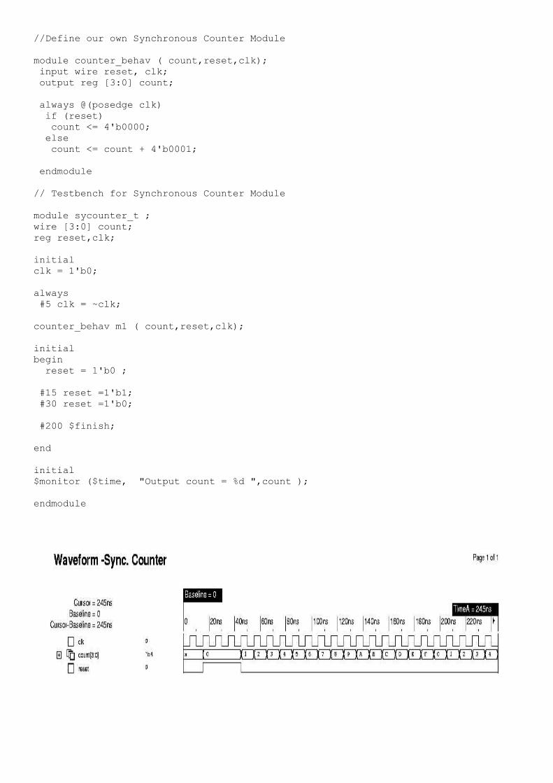
//Define our own Synchronous Counter Module
module counter_behav ( count,reset,clk); input wire reset, clk; output reg [3:0] count;
always @(posedge clk) if (reset) count <= 4'b0000; else count <= count + 4'b0001;
endmodule
// Testbench for Synchronous Counter Module
module sycounter_t ;wire [3:0] count;reg reset,clk; initialclk = 1'b0;
always #5 clk = ~clk;
counter_behav m1 ( count,reset,clk);
initialbegin reset = 1'b0 ;
#15 reset =1'b1; #30 reset =1'b0;
#200 $finish;
end
initial$monitor ($time, "Output count = %d ",count );
endmodule
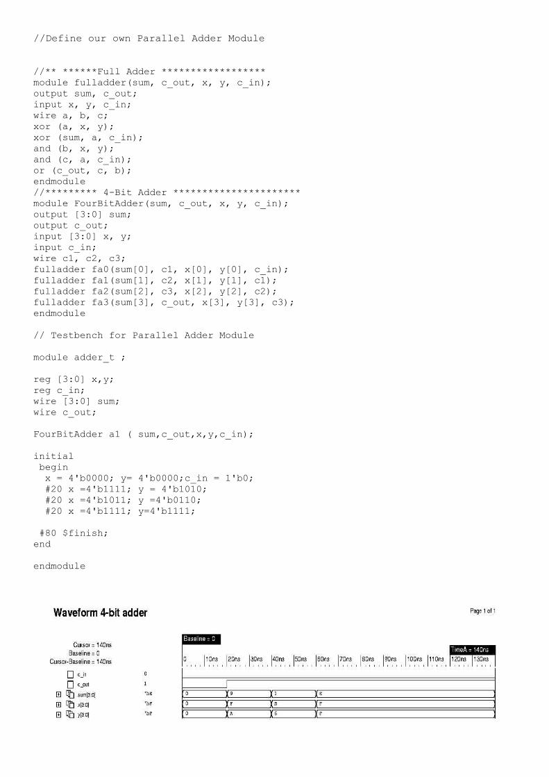
//Define our own Parallel Adder Module
//** ******Full Adder ******************module fulladder(sum, c_out, x, y, c_in);output sum, c_out;input x, y, c_in;wire a, b, c;xor (a, x, y);xor (sum, a, c_in);and (b, x, y);and (c, a, c_in);or (c_out, c, b);endmodule//********* 4-Bit Adder **********************module FourBitAdder(sum, c_out, x, y, c_in);output [3:0] sum;output c_out;input [3:0] x, y;input c_in;wire c1, c2, c3;fulladder fa0(sum[0], c1, x[0], y[0], c_in);fulladder fa1(sum[1], c2, x[1], y[1], c1);fulladder fa2(sum[2], c3, x[2], y[2], c2);fulladder fa3(sum[3], c_out, x[3], y[3], c3);endmodule
// Testbench for Parallel Adder Module
module adder_t ;
reg [3:0] x,y;reg c_in;wire [3:0] sum;wire c_out;
FourBitAdder a1 ( sum,c_out,x,y,c_in);
initial begin x = 4'b0000; y= 4'b0000;c_in = 1'b0; #20 x =4'b1111; y = 4'b1010; #20 x =4'b1011; y =4'b0110; #20 x =4'b1111; y=4'b1111;
#80 $finish;end
endmodule
//Define our own Serial Adder Module
module serial_adder2 (a, b, start, clock, ready, result);
input a, b, start, clock;
output ready;
output [7:0] result;
reg serial_sum, carry_in, carry_out, counting;
reg [3:0] count;
reg [7:0] parallel;
parameter limit = 8;
always @(negedge clock)
begin
if(start)
begin
count = 3'b0;
parallel = 8'b0;
carry_in = 1'b0; counting = 1'b1;
end
else
begin
// adding
{carry_out,serial_sum} = a + b + carry_in ;
carry_in = carry_out;
//shifting
if(counting)
parallel = {serial_sum, parallel [7:1]};
// counting
if (count==limit-1)
counting = 0;
else
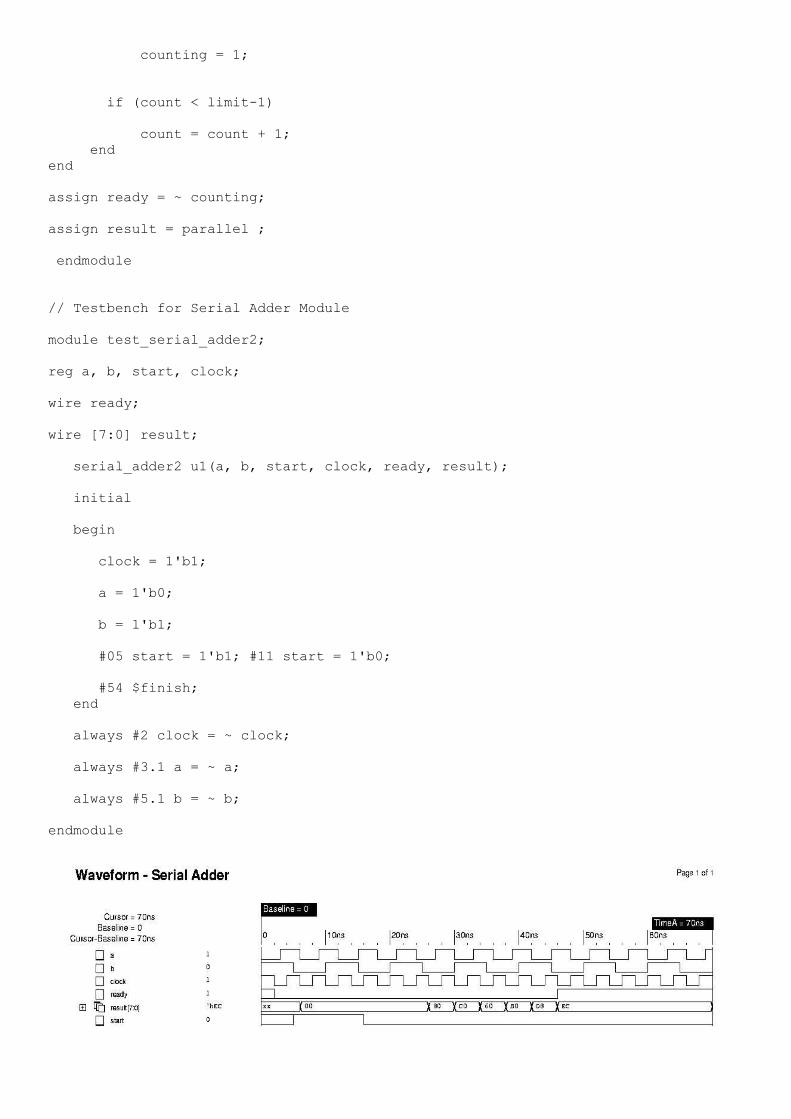
counting = 1;
if (count < limit-1)
count = count + 1; endend
assign ready = ~ counting;
assign result = parallel ;
endmodule
// Testbench for Serial Adder Module
module test_serial_adder2;
reg a, b, start, clock;
wire ready;
wire [7:0] result;
serial_adder2 u1(a, b, start, clock, ready, result);
initial
begin
clock = 1'b1;
a = 1'b0;
b = 1'b1;
#05 start = 1'b1; #11 start = 1'b0;
#54 $finish; end
always #2 clock = ~ clock;
always #3.1 a = ~ a;
always #5.1 b = ~ b;
endmodule
//Define our own Successive Approximation Register Module
module sar(clk,start,ready,indata,bindata);input [31:0]indata;input clk,start;output ready;output [7:0]bindata;
reg [7:0]outdata;reg convert;integer res;parameter limit=8;integer i,j;
always@(negedge clk)begin if(start)
begin outdata=8'b0;
i=1; convert=1'b1;
end else
begin if(convert) begin
outdata[limit-i]=1'b1;res=0;for(j=0;j<=7;j=j+1)begin
if(outdata[j]==1)res=res+2**j;
endif(res>indata)
outdata[limit-i]=1'b0; end i=i+1; if(i>limit+1)
convert=0; else
convert=1;end
end assign ready=~convert; assign bindata=outdata;
endmodule
// Testbench for Successive Approximation Register Module
module sar_t;reg clk;reg [31:0]indata;reg start;wire [7:0]binout;
sar s(clk,start,ready,indata,binout);
initial begin clk=1'b1; indata=170;
#05 start=1'b1; #11 start=1'b0; #50 $finish; endalways #2 clk=~clk;
endmodule


![Mtech Vlsi Lab Manual[1]](https://img.pdfslide.us/doc/110x75/547776245906b569318b4589/mtech-vlsi-lab-manual1.jpg)