Embed Size (px)
DESCRIPTION
VLSI ppt
Citation preview

M.E (VLSI Design)
2013, Regulations, Curriculum & Syllabi
BANNARI AMMAN INSTITUTE OF TECHNOLOGY (An Autonomous Institution Affiliated to Anna University, Chennai
Approved by AICTE - Accredited by NBA New Delhi, NAAC with ‘A’ Grade and ISO 9001:2008 Certified)
SATHYAMANGALAM – 638 401 Erode District Tamil Nadu
Phone : 04295 226000 Fax : 04295 226666 Web:www.bitsathy.ac.in E-mail : [email protected]
Contents
Page No.
Regulations i
Programme Educational Objectives (PEOs) viii
Programme Outcomes (POs) ix
Mapping of PEOs and POs x
Curriculum 2013 1
Syllabi 3
Electives 16
M.E / M. Tech. Rules and Regulations – 2013 Approved in VII Academic Council Meeting held on 18.05.2013
i
Rules and Regulations
M. E. / M. Tech. Programmes (For the batch of students admitted in 2013-2014 and onwards)
NOTE: The regulations hereunder are subject to amendments as may be decided by the Academic Council of the Institute from time to time. Any or all such amendments will be effective from such date and to such batches of students including those already in the middle of the programme) as may be decided by the Academic Council. 1. Conditions for Admission
(i) Candidates for admission to the I Semester of M. E. / M. Tech. degree programme will be
required to satisfy the conditions of admission thereto prescribed by the Anna University, Chennai and Government of Tamil Nadu.
(ii) Part–time candidates should satisfy conditions regarding experience, sponsorship, place of work,
etc., that may be prescribed by Anna University, Chennai from time to time, in addition to satisfying requirements as in Clause 1(i).
2. Duration of the Programme
(i) Minimum Duration: The programme will lead to the Degree of Master of Engineering (M.E.) /
Master of Technology (M. Tech.) of the Anna University, Chennai extend over a period of two years. The two academic years (Part-time three academic years) will be divided into four semesters (Part-time six Semesters) with two semesters per year.
(ii) Maximum Duration: The candidate shall complete all the passing requirements of the M. E. /
M. Tech. degree programmes within a maximum period of 4 years / 8 semesters in case of full-time programme and 6 years / 12 semesters in case of part-time programme, these periods being reckoned from the commencement of the semester to which the candidate was first admitted.
3. Branches of Study
The following are the branches of study of M.E. / M.Tech. Programmes M.E. Branch I Applied Electronics Branch II CAD/CAM Branch III Communication Systems Branch IV Computer Science and Engineering Branch V Embedded Systems Branch VI Engineering Design Branch VII Power Electronics and Drives Branch VIII Software Engineering Branch IX Structural Engineering Branch X VLSI Design Branch XI Biotechnology M. Tech. Branch I Biotechnology
4. Structure of Programmes
(i) Curriculum: The curriculum for each programme includes Courses of study and detailed syllabi. The Courses of study include theory Courses (including electives), seminar, practicals, Industrial
M.E / M. Tech. Rules and Regulations – 2013 Approved in VII Academic Council Meeting held on 18.05.2013
ii
training / Mini-project, Project Work (Phase I) and Project Work (Phase II) as prescribed by the respective Boards of Studies from time to time. Full-time Programme: Every full-time candidate shall undergo the Courses of his/her programme given in clause 12 in various semesters as shown below:
Semester 1: 6 Theory Courses and two Practicals Semester 2: 6 Theory Courses, one Practical and a Technical Seminar Semester 3: 3 Theory Courses and Project Work (Phase I) Semester 4: Project work (Phase II).
Part-time Programme: Every part-time candidate shall undergo the Courses of his/her programme in various semesters as shown below:
Semester 1: 3 Theory Courses and one Practical Semester 2: 3 Theory Courses and one Practical Semester 3: 3 Theory Courses, Technical Seminar and one Practical
Semester 4: 3 Theory Courses Semester 5: 3 Theory Courses and Project Work (Phase I) Semester 6: Project Work (Phase II)
(ii) Theory Courses: Every candidate shall undergo core theory, elective, and practical Courses
including project work of his/her degree programme as given in clause 12 and six elective theory Courses. The candidate shall opt electives from the list of electives relating to his/her degree programme as given in clause 12 in consultation with the Head of the Department. However, a candidate may be permitted to take a maximum of two electives from the list of Courses of other M.E. / M.Tech. Degree programmes with specific permission from the respective Heads of the Departments.
(iii) Project Work: Every candidate individually shall undertake the Project Work (Phase I) during
the third semester (fifth semester for part-time programme) and the Project Work (Phase II) during the fourth semester (Sixth semester for part-time programme). The Project Work (Phase II) shall be a continuation work of the Project Work (Phase I). The Project Work can be undertaken in an industrial / research organisation or in the Institute in consultation with the faculty guide and the Head of the Department. In case of Project Work at industrial / research organization, the same shall be jointly supervised by a faculty guide and an expert from the organization.
(iv) Industrial Training / Mini Project: Every full-time candidate shall opt to take-up either
industrial training or Mini Project under the supervision of a faculty guide. (v) Value added / Certificate Courses: Students can opt for any one of the Value added Courses in
II and III semester. A separate certificate will be issued on successful completion of the Course. (vi) Special Self-Study Elective Courses: Students can opt for any one of the special elective
Courses as Self-Study in addition to the electives specified in the curriculum in II and III semesters, under the guidance of the faculty. The grades of only passed candidates will be indicated in the mark sheet, but will not be taken into account for assessing CGPA.
(vii) Application oriented and Design Experiments: The students are to carryout Application
oriented and Design Experiments in each laboratory in consultation with the respective faculty and Head of the department.
(viii) Mini project: A Mini Project shall be undertaken individually or in a group of not more than 3 in
consultation with the respective faculty and the Heads of the Department, in any one of the laboratories from I to III semesters.

M.E / M. Tech. Rules and Regulations – 2013 Approved in VII Academic Council Meeting held on 18.05.2013
iii
(ix) Credit Assignment: Each course is normally assigned a certain number of credits with 1 credit
per lecture hour per week, 1 credit for 1 or 2 hours of practical per week (2 credits for 3 hours of practical), 4 credits for theory with lab component with 3 hours of lecture and 2 hours of practical per week, 2 credits for 3 hours of seminar per week, 6 credits for the Project Phase I and 12 credits for the Project Phase II. The exact numbers of credits assigned to the different courses of various programmes are decided by the respective Boards of Studies.
(x) Minimum Credits: For the award of the degree, the candidate shall earn a minimum number of total credits as prescribed by the respective Board of Studies as given below:
M.E./M. Tech. Programmes Total Credits M.E. Applied Electronics 75 M.E. CAD / CAM 75 M.E. Communication Systems 75 M.E. Computer Science and Engineering 75 M.E. Embedded Systems 75 M.E. Engineering Design 77 M.E. Power Electronics and Drives 76 M.E. Software Engineering 76 M.E. Structural Engineering 77 M.E. VLSI Design 75 M.Tech. Biotechnology 76
5. Requirements for Completion of Study of a Semester
(i) a) Candidate will be deemed to have completed the study of any semester only if he /she has kept not less than 70% of attendance in each course and at least 80% of attendance on an average in all courses in that semester put together.
b) On medical grounds, 10% relaxation in the attendance can be allowed (ii) his/her progress has been satisfactory, and (iii) his/her conduct has been satisfactory
6. Assessment and Passing Requirements
(i) Assessment: The assessment will comprise continuous assessment and final examination, carrying marks as specified in the scheme (clause 10). Continuous assessment will be made as per the guidelines framed by the Institute from time to time. All assessments will be done on absolute marks basis. However, for the purpose of reporting the performance of a candidate, letter grades and grade points will be awarded as per clause 6(v).
(ii) Final Examinations: Final examinations will normally be conducted during November /
December and during April / May of each year. Supplementary examinations may be conducted at such times as may be decided by the Institute. A candidate will be permitted to appear for the final examination of a semester only if he/she has completed the study of that semester satisfying the requirements given in clause 5 and registers simultaneously for the examinations of the highest semester eligible and all the Courses which he/she is in arrears of. A candidate, who is not permitted to appear at the final examination of a semester, is not permitted to proceed to the next semester. A candidate who is not permitted to appear at the final examination of any semester has to register for and redo the Courses of that semester at the next available opportunity.
(iii) Rejoining the Programme: A candidate who has not completed the study of any semester as per clause 5 or who is allowed to rejoin the programme after a period of discontinuance or who on his/her own request is permitted to repeat the study of any semester, may join the semester which he/she is eligible or permitted to join, only at the time of its normal commencement for a regular
M.E / M. Tech. Rules and Regulations – 2013 Approved in VII Academic Council Meeting held on 18.05.2013
iv
batch of candidates and after obtaining the approval from the Director of Technical Education and Anna University, Chennai. No candidate will however be enrolled in more than one semester at any point of time. In the case of repeaters, the earlier continuous assessment in the repeated Courses will be disregarded.
(iv) Industrial Training, Mini-project and Project Work:
Every candidate shall submit reports on Industrial training / Mini-project, Project Work (Phase I) and Project Work (Phase II) on dates announced by the Institute / department through the faculty guide to the Head of the Department. If a candidate fails to submit the reports of any of these Courses not later than the specified date, he/she is deemed to have failed in it. Every candidate shall present report/papers in the seminars in each of the relevant semesters about the Industrial training / Mini-project, Project Work (Phase I) and Project Work (Phase II). The reports/papers shall be presented in the seminar before a review committee constituted by the Head of the Department. The Industrial training / Mini-project, Project Work (Phase I) and Project Work (Phase II) will be evaluated based on the presentations in the seminar, reports and viva-voce examinations. In case of the industrial training for the full-time candidates, evaluation will be carried out in the third semester.
In case of Project Work (Phase II), the viva-voce examination will be carried out by a team consisting of an internal examiner, usually the supervisor, and an external examiner, appointed by the Principal. 1. Due weight will be given for the training report from the Organisation / Industry while
evaluating the report and its presentation at the seminar about the nature of the training and what the student has learnt. The student shall be required to get a grade not less than “C”. The grade will be indicated in the mark sheet. This will not be taken into account for assessing CGPA.
2. The evaluation of the Mini Project will be based on the report, presentation at the seminar and viva-voce. The student shall be required to get a Grade not less than “C”. The grade will be indicated in the mark sheet. This will not be taken into account for assessing CGPA.
3. Every Candidate shall pursue Project work-Phase I in third semester and Project Work – Phase II in fourth semester which is in continuation of Phase I. Project work –Phase I and Phase II will be evaluated as given below in the scheme of evaluation
A candidate is permitted to register for the Project Work (Phase II), only after passing the Project Work (Phase I). A candidate who fails in Industrial training / Mini-project, Project Work (Phase I) or Project Work (Phase II) shall register for redoing the same at the beginning of a subsequent semester.
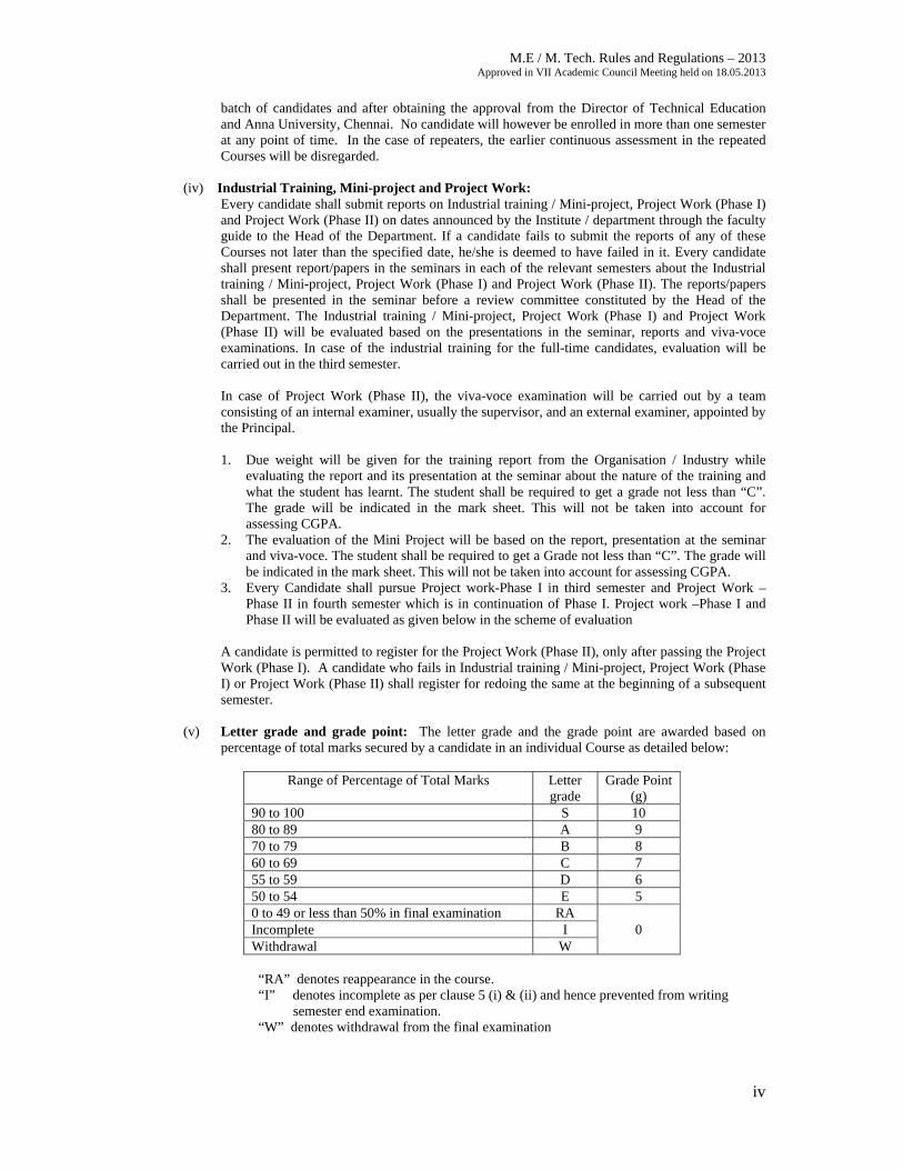
(v) Letter grade and grade point: The letter grade and the grade point are awarded based on percentage of total marks secured by a candidate in an individual Course as detailed below:
Range of Percentage of Total Marks Letter
grade Grade Point
(g) 90 to 100 S 10 80 to 89 A 9 70 to 79 B 8 60 to 69 C 7 55 to 59 D 6 50 to 54 E 5 0 to 49 or less than 50% in final examination RA
0 Incomplete I Withdrawal W
“RA” denotes reappearance in the course. “I” denotes incomplete as per clause 5 (i) & (ii) and hence prevented from writing semester end examination. “W” denotes withdrawal from the final examination
M.E / M. Tech. Rules and Regulations – 2013 Approved in VII Academic Council Meeting held on 18.05.2013
v
After completion of the programme earning the minimum number of credits, the Cumulative Grade Point Average (CGPA) from the semester in which the candidate has joined first to the final semester is calculated using the formula:
CGPA = ∑
∑i
ii
CCg *
Where ig : Grade point secured corresponding to the Course
iC : Credits allotted to the Course. (vi) Passing a Course: A candidate who secures grade point 5 or more in any Course of study will be
declared to have passed that Course, provided a minimum of 50% is secured in the final examination of that Course of study.
A candidate, who is absent for the final examination or withdraws from final examination or secures a letter grade RA (Grade point 0) in any Course carrying continuous assessment and final examination marks, will retain the already earned continuous assessment marks for two subsequent appearances in the examination of that Course and thereafter he/she will be solely assessed by the final examination carrying the entire marks of that Course.
A candidate, who scores a letter grade RA (Grade point 0) in any Course carrying only continuous assessment marks, will be solely examined by a final examination carrying the entire marks of that Course, the continuous assessment marks obtained earlier being disregarded.
7. Qualifying for the Award of the Degree
A candidate will be declared to have qualified for the award of the M.E. / M.Tech. Degree provided:
(i) he/she has successfully completed the Course requirements and has passed all the prescribed Courses of study of the respective programme listed in clause 12 within the duration specified in clause 2.
(ii) No disciplinary action is pending against the candidate
8. Classification of Degree
(i) First Class with Distinction: A candidate who qualifies for the award of degree (vide clause 7) having passed all the Courses of all the semesters at the first opportunity within four consecutive semesters (six consecutive semesters for part-time) after the commencement of his / her study and securing a CGPA of 8.5 and above shall be declared to have passed in First Class with Distinction. For this purpose the withdrawal from examination (vide clause 9) will not be construed as an opportunity for appearance in the examination.
(ii) First Class: A candidate who qualifies for the award of degree (vide clause 7) having passed all the Courses of all the semesters within a maximum period of six semesters for full-time and eight consecutive semesters for part-time after commencement of his /her study and securing a CGPA of 6.50 and above shall be declared to have passed in First Class.
(iii) Second Class: All other candidates who qualify for the award of degree (vide clause 7) shall be declared to have passed in Second Class.
9. Withdrawal from Examination
(i) A candidate may, for valid reasons, be granted permission to withdraw from appearing for the examination in any Course or Courses of only one semester examination during the entire duration of the degree programme. Also, only one application for withdrawal is permitted for that semester examination in which withdrawal is sought.
(ii) Withdrawal application shall be valid only if the candidate is otherwise eligible to write the examination and if it is made prior to the commencement of the semester examinations and also recommended by the Head of the Department and the Principal.
M.E / M. Tech. Rules and Regulations – 2013 Approved in VII Academic Council Meeting held on 18.05.2013
vi
(iii) Withdrawal shall not be construed as an opportunity for appearance in the examination for the eligibility of a candidate for First Class with Distinction.
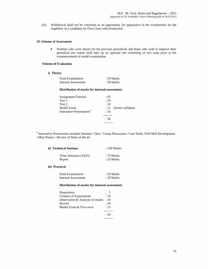
10. Scheme of Assessment
• Students who were absent for the previous periodicals and those who wish to improve their periodical test marks shall take up an optional test consisting of two units prior to the commencement of model examination.
Scheme of Evaluation
i) Theory
Final Examination : 50 Marks Internal Assessment : 50 Marks Distribution of marks for internal assessment: Assignment/Tutorial : 05
Test 1 : 10 Test 2 : 10 Model Exam : 15 (Entire syllabus) Innovative Presentation# : 10
--------- : 50
--------- # Innovative Presentation includes Seminar / Quiz / Group Discussion / Case Study /Soft Skill Development / Mini Project / Review of State-of-the art
ii) Technical Seminar : 100 Marks
Three Seminars (3X25) : 75 Marks Report : 25 Marks
iii) Practical
Final Examination : 50 Marks Internal Assessment : 50 Marks
Distribution of marks for internal assessment:
Preparation : 5 Conduct of Experiments : 10
Observation & Analysis of results : 10 Record : 10 Model Exam & Viva-voce : 15 ---------
: 50 ---------
M.E / M. Tech. Rules and Regulations – 2013 Approved in VII Academic Council Meeting held on 18.05.2013
vii
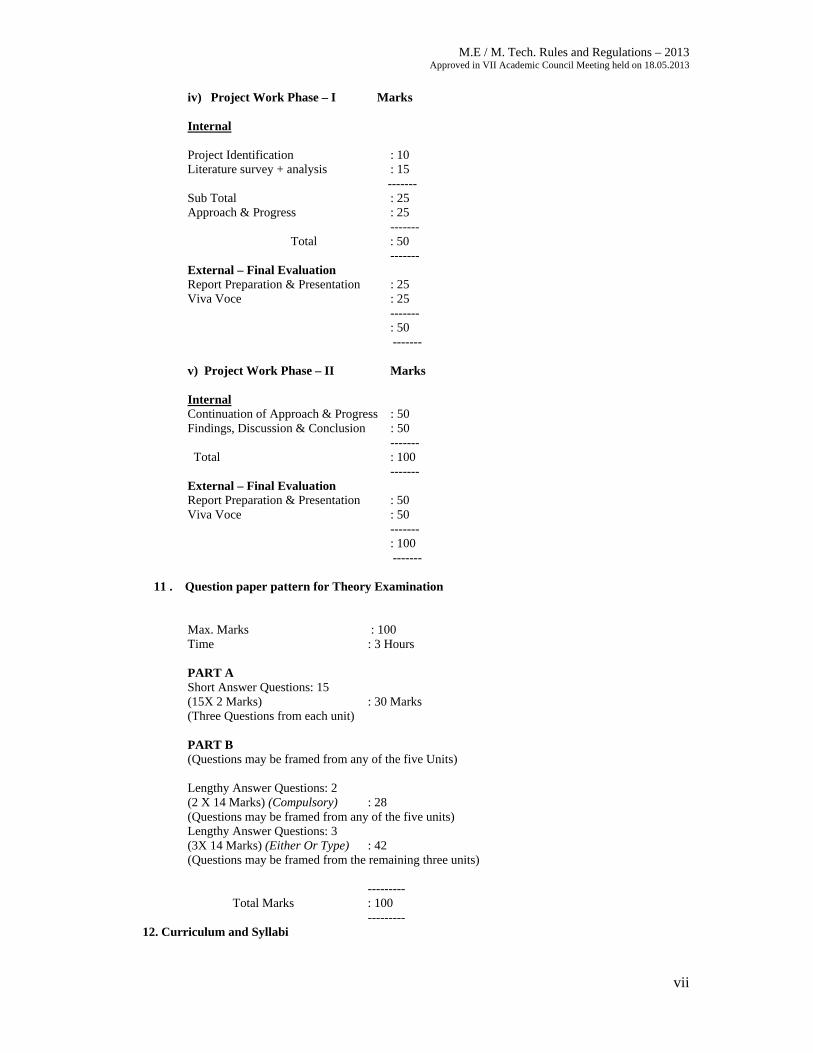
iv) Project Work Phase – I Marks
Internal Project Identification : 10 Literature survey + analysis : 15 ------- Sub Total : 25 Approach & Progress : 25 ------- Total : 50 ------- External – Final Evaluation Report Preparation & Presentation : 25 Viva Voce : 25 ------- : 50 ------- v) Project Work Phase – II Marks Internal Continuation of Approach & Progress : 50 Findings, Discussion & Conclusion : 50 ------- Total : 100 ------- External – Final Evaluation Report Preparation & Presentation : 50 Viva Voce : 50 ------- : 100 -------
11 . Question paper pattern for Theory Examination
Max. Marks : 100
Time : 3 Hours
PART A Short Answer Questions: 15
(15X 2 Marks) : 30 Marks (Three Questions from each unit)
PART B (Questions may be framed from any of the five Units)
Lengthy Answer Questions: 2 (2 X 14 Marks) (Compulsory) : 28 (Questions may be framed from any of the five units) Lengthy Answer Questions: 3 (3X 14 Marks) (Either Or Type) : 42 (Questions may be framed from the remaining three units)
---------
Total Marks : 100 --------- 12. Curriculum and Syllabi
PEOs & POs M. E. VLSI Design| Regulation 2013
Approved in the IX Academic Council held on 07-12-2013
viii
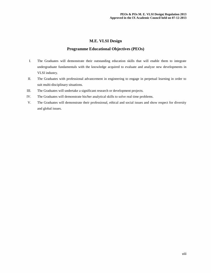
M.E. VLSI Design
Programme Educational Objectives (PEOs)
I. The Graduates will demonstrate their outstanding education skills that will enable them to integrate
undergraduate fundamentals with the knowledge acquired to evaluate and analyze new developments in
VLSI industry.
II. The Graduates with professional advancement in engineering to engage in perpetual learning in order to
suit multi-disciplinary situations.
III. The Graduates will undertake a significant research or development projects.
IV. The Graduates will demonstrate his/her analytical skills to solve real time problems.
V. The Graduates will demonstrate their professional, ethical and social issues and show respect for diversity
and global issues.
PEOs & POs M. E. VLSI Design| Regulation 2013
Approved in the IX Academic Council held on 07-12-2013
ix
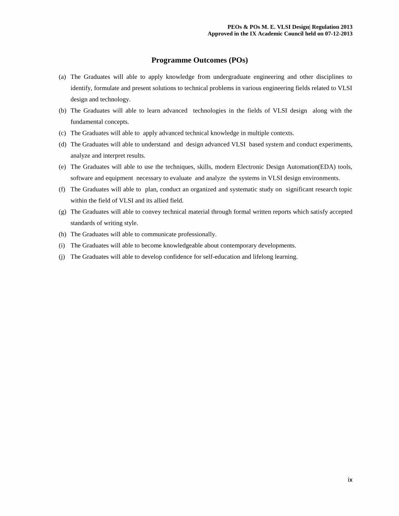
Programme Outcomes (POs)
(a) The Graduates will able to apply knowledge from undergraduate engineering and other disciplines to
identify, formulate and present solutions to technical problems in various engineering fields related to VLSI
design and technology.
(b) The Graduates will able to learn advanced technologies in the fields of VLSI design along with the
fundamental concepts.
(c) The Graduates will able to apply advanced technical knowledge in multiple contexts.
(d) The Graduates will able to understand and design advanced VLSI based system and conduct experiments,
analyze and interpret results.
(e) The Graduates will able to use the techniques, skills, modern Electronic Design Automation(EDA) tools,
software and equipment necessary to evaluate and analyze the systems in VLSI design environments.
(f) The Graduates will able to plan, conduct an organized and systematic study on significant research topic
within the field of VLSI and its allied field.
(g) The Graduates will able to convey technical material through formal written reports which satisfy accepted
standards of writing style.
(h) The Graduates will able to communicate professionally.
(i) The Graduates will able to become knowledgeable about contemporary developments.
(j) The Graduates will able to develop confidence for self-education and lifelong learning.

PEOs & POs M. E. VLSI Design| Regulation 2013
Approved in the IX Academic Council held on 07-12-2013
x
Mapping of PEOs & POs
Programme Educational Objectives Program Outcomes
PEO: I The Graduates of VLSI Design will demonstrate
their outstanding education skills that will enable
them to integrate undergraduate fundamentals
with the knowledge acquired to evaluate and
analyze new developments in VLSI industry.
(a),(b)
PEO: II The Graduates of VLSI Design will demonstrate
advancement in engineering to engage in
perpetual learning in order to suit multi-
disciplinary situations.
(c),(f)
PEO: III The Graduates of VLSI Design would undertake
a significant research or development projects.
(d),(e),(g)
PEO: IV The VLSI Design Graduates would demonstrate
his/her analytical skills to solve real time
problems.
(h),(i)
PEO: V The VLSI Design Graduates will demonstrate
their professional, ethical and social issues and
show respect for diversity and global issues.
(j)
Curriculum of M. E. VLSI Design| Minimum Credits to be earned: 75| Regulation 2013
Approved in the IX Academic Council held on 07-12-2013
1
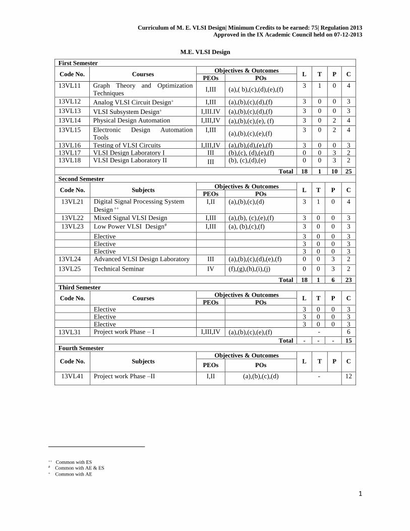
M.E. VLSI Design
Common with ES # Common with AE & ES Common with AE
First Semester
Code No. Courses Objectives & Outcomes
L T P C PEOs POs
13VL11 Graph Theory and Optimization
Techniques I,III (a),( b),(c),(d),(e),(f)
3 1 0 4
13VL12 Analog VLSI Circuit Design I,III (a),(b),(c),(d),(f) 3 0 0 3
13VL13 VLSI Subsystem Design I,III.IV (a),(b),(c),(d),(f) 3 0 0 3
13VL14 Physical Design Automation I,III,IV (a),(b),(c),(e), (f) 3 0 2 4
13VL15 Electronic Design Automation
Tools I,III
(a),(b),(c),(e),(f) 3 0 2 4
13VL16 Testing of VLSI Circuits I,III,IV (a),(b),(d),(e),(f) 3 0 0 3 13VL17 VLSI Design Laboratory I III (b),(c), (d),(e),(f) 0 0 3 2 13VL18 VLSI Design Laboratory II III (b), (c),(d),(e) 0 0 3 2
Total 18 1 10 25
Second Semester
Code No. Subjects Objectives & Outcomes
L T P C PEOs POs
13VL21 Digital Signal Processing System
Design
I,II (a),(b),(c),(d) 3 1 0 4
13VL22 Mixed Signal VLSI Design I,III (a),(b), (c),(e),(f) 3 0 0 3
13VL23 Low Power VLSI Design# I,III (a), (b),(c),(f) 3 0 0 3
Elective 3 0 0 3 Elective 3 0 0 3 Elective 3 0 0 3
13VL24 Advanced VLSI Design Laboratory III (a),(b),(c),(d),(e),(f) 0 0 3 2
13VL25 Technical Seminar IV (f),(g),(h),(i),(j) 0 0 3 2
Total 18 1 6 23
23 Third Semester
Code No. Courses Objectives & Outcomes
L T P C PEOs POs
Elective 3 0 0 3 Elective
3 0 0 3 Elective 3 0 0 3
13VL31 Project work Phase – I
I,III,IV (a),(b),(c),(e),(f) -
-
-
6
Total - - - 15
Fourth Semester
Code No. Subjects Objectives & Outcomes
L T P C PEOs POs
13VL41
Project work Phase –II I,II (a),(b),(c),(d) -
12

Curriculum of M. E. VLSI Design| Minimum Credits to be earned: 75 | Regulation 2013
Approved in the IX Academic Council held on 07-12-2013
2
+ Common with AE * Open Electives $ Common with AE & CO # Common with AE & ES ++ Common with ES
List of Electives
Code No. Courses Objectives & Outcomes
L T P C PEOs POs
13VL51 ASIC Design# I,III (a),(b),(c),(d),(e) 3 0 0 3
13VL52 Hardware Description Language I,III (a),(b),(c),(d) 3 0 0 3
13VL53 System on Chip++ I,III.IV (a),(b),(c) 3 0 0 3
13VL54 Processors and Embedded controllers I,III,IV (a),(b),(c),(d) 3 0 0 3
13VL55 Digital System Design I,III (a),(b),(c),(d) 3 0 0 3
13VL56 Advanced Digital Signal Processing I,III,IV (a),(b),(c),(e),(f) 3 0 0 3
13VL57 Communication Networks$ III (a),(b),(c),(d) 3 0 0 3
13VL58 VLSI for Wireless Communication+++ III (a),(b),(c),(d),(e),(f) 3 0 0 3
13VL59 Semiconductor Memory Design I,III (a),(b),(c),(d),(e) 3 0 0 3
13VL60 ARM Processor and Applications I,III (a),(b),(c),(d) 3 0 0 3
13VL61 Nano Electronics I,III.IV (a),(b),(c),(d),(e) 3 0 0 3
13VL62 Hardware Design Verification Techniques I,III,IV (a),(b),(c),(d) 3 0 0 3
13VL63 Embedded Networking ++ I,III (a),(b),(c),(d),(e),(f) 3 0 0 3
13VL64 VLSI Technology+ I,III,IV (a),(b),(c) 3 0 0 3
13VL65 System Design using FPGA III (a),(b),(c),(d),(e) 3 0 0 3
13VL66 VLSI Signal Processing+ III (a),(b),(c),(d),(e) 3 0 0 3
13VL67 Three Dimensional Network on chip++ I,III (a),(b),(c),(d),(e),(f) 3 0 0 3
13VL68 Reconfigurable Architectures I,III (a),(b),(c),(d),(e) 3 0 0 3
13VL69 Genetic algorithms and their Applications* I,III,IV (a),(b),(c),(d),(e) 3 0 0 3
13VL70 MEMS* I,III (a),(b),(c),(d),(e),(f) 3 0 0 3
Self Study Electives
Code No. Subjects Objectives & Outcomes
L T P C PEOs POs
13VL01 Neural computing+ I,III,IV (a),(b),(c),(d),(e) - - - 3
13VL02 Multimedia Compression Technique$ I,III (a),(b),(c) - - - 3
Syllabi: M. E. VLSI Design (Core) | Minimum Credits to be earned: 75 | Regulation 2013
Approved in the IX Academic Council held on 07-12-2013
3
13VL11 GRAPH THEORY AND OPTIMIZATION TECHNIQUES
3 1 0 4
Objectives
To construct simple mathematical proofs and possess the ability to verify them.
Acquire the knowledge of interest in graph theory and its many applications and to study the concepts of
Eulerian, Hamiltonian Graphs.
Ability to obtain the optimum solutions of Linear Programming Problems, and Dynamic programming.
Course Outcomes (COs)
Explain basic definitions and properties associated with simple planar graphs.
Understand how to solve isomorphism, connectivity, and Euler's formula.
Select and implement appropriate formulations and algorithms from graph theory.
Choose an appropriate method to solve a practical problem.
Programme Outcomes (POs)
(a) Apply basic principles and practices of computing grounded in mathematics and science to successfully
complete software related projects to meet customer business objectives and/or productively engage in
research.
(b) An ability to demonstrate basic competence in electronics and electrical engineering design.
and analysis using applications of mathematics, physics and engineering principles.
(c) An ability to apply engineering tools and techniques to conduct engineering VLSI design.
experiments as well as to analyze and interpret data.
(d) An ability to develop confidence for self learning and life- long learning.
(e) Manage resources like men, money, machinery and material with modern management tools.
(f) An ability to participate and succeed in competitive examinations.
Unit I
Basic Concepts in Graph Theory
Undirected graph-degree of a vertex, degree sequence, sub graphs, vertex induced sub graphs. Complement of a
graph, self complementary graphs, walk, path, connectivity, eccentricity, radius, diameter, vertex and edge cuts,
vertex partition, independent set, clique.
9 Hours
Unit II
Special Classes of Graphs
Digraph- orientation, strongly, weakly and unilaterally connected digraphs, directed acyclic graph. Adjacency
matrix and incidence matrix of graphs. Trees, Spanning Trees, Matrix Tree theorem. Complete graphs, Bipartite
graphs, Grid graphs.
9 Hours
Unit III
Eulerian, Hamiltonian Graphs
Eulerian graphs- Euler’s theorem, Hamiltonian graphs- Bondy- Chvatal theorem, traveling salesman problem. Planar
graphs- Euler’s formula, Kuratowski’s theorem, embedding and dual graphs
9 Hours
Unit IV
Linear Programming
Definition, Simplex, two-phase simplex- Big M-method and dual simplex algorithms.
9 Hours
Unit V
Dynamic Programming
Multistage decision process, Computational procedure, Final and Initial value problems, Continuous Dynamic
programming, Discrete Dynamic programming.
9 Hours
Total: 45+15 Hours
Reference(s)
1. J.Yellen and J. Gross, Graph Theory and its Applications, Chapman & Hall, 2006.
2. H.A.Taha, Operations Research, Prentice Hall, 2003.
3. Narsingh Deo, Graph Theory with Applications to Engineering and Computer Science. Prentice Hall, 2004.
Syllabi: M. E. VLSI Design (Core) | Minimum Credits to be earned: 75 | Regulation 2013
Approved in the IX Academic Council held on 07-12-2013
4
4. D.B .West, Introduction to Graph Theory, Pearson Education, 2007.
5. W.Kocay and D.L.Kreher, Graphs, Algorithms and Optimization, Chapman & Hall, 2006.
13VL12 / 13AE12 ANALOG VLSI CIRCUIT DESIGN
3 0 0 3
Objectives
To understand the operation of BJTs and MOS devices.
To analyze various devices in small and large signal conditions.
To impart in-depth knowledge about switched capacitors, ADCs and DACs.
Course Outcomes (COs)
To acquire knowledge of how a circuit works.
To learn to analyze the circuit.
To view analog integrated circuit design from a hierarchical viewpoint.
To realize schematic of the circuit, dc currents, and W/L ratio.
Programme Outcomes (POs)
(a) able to apply knowledge from undergraduate engineering and other disciplines to identify, formulate and
present solutions to technical problems in various engineering fields related to VLSI design and
technology.
(b) able to learn advanced technologies in the fields of VLSI design along with the fundamental concepts.
(c) able to apply advanced technical knowledge in multiple contexts.
(d) able to understand and design advanced VLSI based system and conduct experiments, analyze and
interpret results.
(f) able to plan, conduct an organized and systematic study on significant research topic within the field of
VLSI and its allied field
Unit I
CMOS Technology and Device Modeling
Basic MOS semiconductor fabrication processes-other considerations of CMOS technology-MOS large signal
model and parameters-Small signal model for the MOS transistor-Computer simulation models-Sub threshold MOS
model.
9 Hours
Unit II
Analog CMOS Sub circuits, CMOS Amplifiers
MOS switch-MOS diode and active resistor-Current sinks and sources-Current mirrors-Current and voltage
References:-Band gap References:-Invertors-Differential amplifiers - Cascode amplifiers – Current amplifiers -
Output amplifiers- High gain amplifiers architectures.
9 Hours
Unit III
High-Performance CMOS Operational Amplifiers
Buffered operational amplifiers-High speed and frequency operational amplifiers-Differential output operational
amplifiers-Microwave operational amplifiers - Low noise operational amplifiers - Low voltage operational
amplifiers.
9 Hours
Unit IV
Switched Capacitor Circuits
Switched Capacitor Circuits-Switched Capacitor amplifiers-Switched Capacitor integrators-z domain models of two
phase switched capacitor circuits-First order switched capacitor circuits- Second order switched capacitor circuits-
Switched Capacitor Filters.
9 Hours
Unit V
Digital to Analog and Analog to Digital Converters
Introduction and characterization of DAC-Parallel DAC-Extending the resolution of parallel DAC-Serial DAC-
Introduction and characterization of ADC-Serial ADC-Medium ADC-High speed ADC.
9 Hours
Total: 45 Hours
Syllabi: M. E. VLSI Design (Core) | Minimum Credits to be earned: 75 | Regulation 2013
Approved in the IX Academic Council held on 07-12-2013
5
Reference(s)
1. Phillip E.Allen and Douglas R.Holberg, CMOS Analog Circuit Design, Oxford University Press, 2002.
2. Malcom R.Haskard and Lan C.May, Analog VLSI Design - NMOS and CMOS, Prentice Hall, 1998.
3. Jose E.France and Yannis Tsividis, Design of Analog-Digital VLSI Circuits for Telecommunication and
Signal Processing, Prentice Hall, 1994.
4. Randall L Geiger, Phillip E. Allen and Noel K.Strader, VLSI Design Techniques for Analog and Digital
Circuits, Mc Graw Hill International Company, 1990.
5. K.Radhakrishna Rao, Electronics for Analog Signal Processing-I, NPTEL, Courseware, 2005.
13VL13 / 13AE67 VLSI SUBSYSTEM DESIGN
3 0 0 3
Objectives:
To learn the basic MOS Circuits
To learn the MOS Process Technology
To understand the operation of MOS devices.
To impart in-depth knowledge about analog and digital CMOS circuits.
Course Outcomes (CO’s)
Analysis the operation of CMOS
Analysis of the design rules and layout diagramf
Design of low power Adders and Multipliers
Analysis the physical design process of VLSI design flow.
Design of CMOS Memories.
Programme Outcomes (POs)
a) able to apply knowledge from undergraduate engineering and other disciplines to identify, formulate and
present solutions to technical problems in various engineering fields related to VLSI design and
technology.
b) able to learn advanced technologies in the fields of VLSI design along with the fundamental concepts.
c) able to apply advanced technical knowledge in multiple contexts.
d) able to understand and design advanced VLSI based system and conduct experiments, analyze and
interpret results.
f) able to plan, conduct an organized and systematic study on significant research topic within the
field of VLSI and its allied field
Unit I
MOS Circuit Design Process Overview of VLSI Design Methodology VLSI design process- Basic MOS transistors- Enhancement mode
transistor operation - Drain current Vs voltage derivation -NMOS inverter- Determination of pull up to pull down
ratio for an NMOS inverter-CMOS inverter - DC Characteristics- Switching Characteristics – Power dissipation.
9 Hours
Unit II
Logic Design
Pass transistor and transmission gate – static CMOS design, Pseudo NMOS, and dynamic CMOS logic – Clocked
CMOS logic – domino logic- Precharged domino logic, Dual rail logic with suitable examples.
9 Hours
Unit III
Sequential Logic
Clocked sequential circuits – Two phase clocking – charge storage – dynamic sequential circuits – JK Flip-flop
circuit, Memory Design-DRAM, SRAM and Flash Memory.
9 Hours
Unit IV
Datapath Subsystem
Introduction, Design of Adders: carry look ahead - carry select - carry save, One/Zero Detector, Comparator-
Magnitude, Equality, Counters-Binary Counter, LFSR, Parity generators.
9 Hours
Syllabi: M. E. VLSI Design (Core) | Minimum Credits to be earned: 75 | Regulation 2013
Approved in the IX Academic Council held on 07-12-2013
6
Unit V
VLSI Building Block Design
PLA design – Arithmetic logic unit design- Design of multipliers: Parallel Multipliers, Array, 2’s Complement,
Booth - Braun – Baugh - Wooley - Wallace tree, Dadda Multipliers, Serial Multiplication.
9 Hours
Total: 45 Hours
Reference(s)
1. Kamran Eshraghian, Douglas A. Pucknell, Essentials of VLSI Circuits and Systems, Prentice Hall of India,
2011
2. John P.Uyemura, Introduction to VLSI circuits and systems, John Wiley & Sons, 2012.
3. Neil Weste and Kamran Eshranghian, Principles of CMOS VLSI Design, Addison Wiley, 2012.
4. Jan M Rabaey, Digital Integrated Circuits- A Design, Prentice Hall, 2009.
5. C.Mead and L.Conway, Introduction to VLSI Systems, Addison Wesley, 1999.
6. Kang, CMOS Digital integrated Circuits, McGraw Hill, 2002.
7. L.Glaser and D.Dobberpuhl, The Design and Analysis of VLSI Circuits, Addison Wesley, 1995.
8. S.Srinivasan, VLSI Circuits, NPTEL Courseware, 2005.
13VL14 PHYSICAL DESIGN AUTOMATION
3 0 2 4
Objectives
To understand the concepts of VLSI Design Automation.
To understand the concepts of Physical Design Process such as Partitioning, Floorplanning, Placement and
Routing.
To understand the concepts of Simulation and Synthesis in VLSI Design Automation.
Course Outcomes (COs)
To acquire knowledge of how Physical design works.
To learn to analyze the problems in Physical design.
To view VLSI design from a hierarchical viewpoint.
Programme Outcomes (POs)
(a) able to apply knowledge from undergraduate engineering and other disciplines to identify, formulate and
present solutions to technical problems in various engineering fields related to VLSI design and
technology.
(b) able to learn advanced technologies in the fields of VLSI design along with the fundamental concepts.
(c) able to apply advanced technical knowledge in multiple contexts
(e) able to use the techniques, skills, modern Electronic Design Automation(EDA) tools, software and
equipment necessary to evaluate and analyze the systems in VLSI design environments.
(f) able to plan, conduct an organized and systematic study on significant research topic within the field of
VLSI and its allied field.
Unit I
VLSI Design Automation and Floor planning Introduction to Design methodologies – VLSI physical design automation –Computational Complexity- Tractable
and Intractable Problems - Floor planning concepts -shape functions and floor plan sizing
9 Hours
Unit II
Placement and Routing Placement and partitioning - Circuit representation - Placement algorithms – partitioning - Types of local routing
problems - Area routing - channel routing - global routing - algorithms for global routing
9 Hours
Unit III
Layout Compaction and Performance Issues in Circuit Layout Layout Compaction - Design rules - problem formulation - algorithms for constraint graph compaction-Delay
models-Timing Driven Placement-Timing Driven Routing- Via Minimization-Power Minimization.
9 Hours
Syllabi: M. E. VLSI Design (Core) | Minimum Credits to be earned: 75 | Regulation 2013
Approved in the IX Academic Council held on 07-12-2013
7
Unit IV
Single Layer Routing and Logic Synthesis
Wire length and bend minimization technique–Over the Cell (OTC) Routing – Introduction to Combinational Logic
Synthesis - Binary Decision Diagrams - Two Level Logic Synthesis.
9 Hours
Unit V
High level Synthesis
Hardware models - Internal representation - Allocation assignment and scheduling - Simple scheduling algorithm -
Assignment problem – High level transformations.
9 Hours
Lab Components
1. Design and Development of Partitioning algorithms.
2. Draw the layout of simple combinational circuit.
3. Simulation and synthesis of Sequential Circuit.
15 Hours
Total: 45+15 Hours
Reference(s)
1. H.Gerez, Algorithms for VLSI Design Automation, John Wiley & Sons, 2002.
2. Sarafzadeh,C.K.Wong, An Introduction to VLSI Physical Design, Mc Graw Hill International Edition 1995.
3. N.A Sherwani, Algorithms for VLSI Physical Design Automation, Kluwer Academic Publishers, 2002.
4. R .Drechsler, Evolutionary Algorithms for VLSI CAD, Boston, Kluwer Academic Publishers, 2010.
5. D.Hill, D.Shugard, J.Fishburn and K.Keutzer, Algorithms and Techniques for VLSI Layout Synthesis,
Kluwer Academic Publishers, Boston, 1990.
13VL15 ELECTRONIC DESIGN AUTOMATION TOOLS
3 0 2 4
Objectives
To study the concepts of simulation and synthesis of HDLs.
To understand the concepts of SPICE and circuit simulation using Spice.
To study the concepts of S-edit and Layout design using S-edit.
Course Outcomes (COs)
Explain basic definitions and overview of different tools.
Understand how to solve simulation, Synthesis of HDLs.
Select and implement appropriate formulations and algorithms from SPICE.
Choose an appropriate method to design an S-edit.
Programme Outcomes (POs)
[[[
(a) able to apply knowledge from undergraduate engineering and other disciplines to identify, formulate and
present solutions to technical problems in various engineering fields related to VLSI design and
technology.
(b) able to learn advanced technologies in the fields of VLSI design along with the fundamental concepts.
(c) able to apply advanced technical knowledge in multiple contexts
(e) able to use the techniques, skills, modern Electronic Design Automation(EDA) tools, software and
equipment necessary to evaluate and analyze the systems in VLSI design environments.
(f) able to plan, conduct an organized and systematic study on significant research topic within the field of
VLSI and its allied field
Unit I
Basics of EDA
VLSI Design Automation tools-An overview of the features of practical CAD tools – Modelsim - Leonardo
spectrum -Xilinx ISE - Quartus II - VLSI backend tools –IC Station, Cadence and Synopsis.
9 Hours
Unit II
Simulation of HDLs
Different types of Hardware modeling with HDL – Types of Simulation - Sequential and concurrent statements in
VHDL – Procedures, assignments and control statements in Verilog.
9 Hours
Syllabi: M. E. VLSI Design (Core) | Minimum Credits to be earned: 75 | Regulation 2013
Approved in the IX Academic Council held on 07-12-2013
8
Unit III
Synthesis of HDLs
Logic synthesis in Verilog – Logic synthesis in VHDL - Finite State Machines synthesis in Verilog – Finite State
Machines synthesis in VHDL - Memory synthesis in Verilog – Memory synthesis in VHDL - Performance driven
synthesis.
9 Hours
Unit IV
Simulation of SPICE
Circuit description - DC circuit analysis- Transient analysis - AC circuit analysis - Advanced spice commands and
analysis- Models for Semiconductor diodes - Models for Bipolar Junction Transistors - Models for Field Effect
Transistors.
9 Hours
Unit V
Schematic and Layout design
Creating a project- Drawing, Selecting and Editing objects -Creating a schematic - Creating a symbol - Importing
and Exporting Net lists and Schematics - Simulation and Waveform probing.
9 Hours
Lab Components
1. Design of D Flipflop.
2. Design of 2/3 Prescaler.
3. Design of Vending Machine Controller using FSM.
15 Hours
Total: 45+15 Hours
Reference(s)
1. M.J.S.Smith, Application Specific Integrated Circuits, Pearson Education, 2008.
2. M.H.Rashid, Spice for Circuits and Electronics using Pspice, PHI 1995.
3. S-Edit v13.0 user guide by Tanner EDA tool.
4. J.Bhaskar, Verilog Synthesis Primer, Prentice Hall, 1998.
5. J.Bhaskar, A VHDL Primer, Prentice Hall, 1998.
6. J.Bhaskar, A Verilog Primer, Prentice Hall, 2005.
13VL16 TESTING OF VLSI CIRCUITS
3 0 0 3
Objectives:
To understand about testing, fault models and types of simulations.
To acquire knowledge in generation of test vectors for combinational and sequential circuits.
To understand the concepts behind testable design, BIST and fault diagnosis.
Course Outcomes (CO’s)
Ability to know about importance of testing and its types in VLSI circuits.
Ability to model different faults and carry out fault simulation in digital circuits.
Ability to determine fault oriented test vectors for single stuck-at-faults in combinational and Sequential
circuits.
Ability to design digital VLSI circuits with DFT and BIST techniques.
Programme Outcomes (POs)
(a) able to apply knowledge from undergraduate engineering and other disciplines to identify, formulate and
present solutions to technical problems in various engineering fields related to VLSI design and
technology.
(b) able to learn advanced technologies in the fields of VLSI design along with the fundamental concepts.
(d) able to understand and design advanced VLSI based system and conduct experiments, analyze and
interpret results.
(e) able to use the techniques, skills, modern Electronic Design Automation(EDA) tools, software and
equipment necessary to evaluate and analyze the systems in VLSI design environments.
(f) able to plan, conduct an organized and systematic study on significant research topic within the field of
VLSI and its allied field.
Syllabi: M. E. VLSI Design (Core) | Minimum Credits to be earned: 75 | Regulation 2013
Approved in the IX Academic Council held on 07-12-2013
9
Unit I
Fault Simulation
Introduction to Testing - Faults in digital circuits - Modeling of faults - Logical Fault Models - Fault detection -
Fault location - Fault dominance - Logic Simulation - Types of simulation - Delay models - Gate level Event-driven
simulation.
9 Hours
Unit II
Test Generation
Test generation for combinational logic circuits - Testable combinational logic circuit design - Test generation for
sequential circuits - design of testable sequential circuits- Adhoc design and scan based design techniques.
9 Hours
Unit III
Analog and Mixed Signal Test
DSP based analog and mixed signal test – Static ADC and DAC testing methods - Model based Analog and Mixed
signal Test- Analog fault models-Analog fault simulation – Analog ATPG
9 Hours
Unit IV
Built In Self Test
Built-In Self Test - Test pattern generation for BIST - Circular BIST - BIST Architectures – BEST – LOCST -
STUMPS - CATS – BILBO - Testable Memory Design - Test algorithms - Test generation for Embedded RAMs
9 Hours
Unit V
Fault Diagnosis
Logic Level Diagnosis - Diagnosis by UUT reduction - Fault Diagnosis for Combinational Circuits - Self-checking
design: error detecting and correcting codes, self checking combinational logic, sequential logic design : Faults in
State Machines , Self-Checking State Machine Design Techniques, Elimination of Bidirectional Errors
9 Hours
Total: 45 Hours
Reference(s)
1. Abramovici .M, Breuer M.A and Friedman A.D, Digital Systems and Testable Design, Jaico Publishing
House, 2002.
2. Bushnell M.L and Agrawal V.D, Essentials of Electronic Testing for Digital, Memory and Mixed-Signal
VLSI Circuits, Kluwer Academic Publishers, 2002.
3. Lala P.K, Digital Circuit Testing and Testability, Academic Press, 2002.
4. Parag K. Lala, Self-checking and fault-tolerant digital design, Morgan Kaufmann ,2001.
5. Xiaoqing Wen, Cheng Wen Wu and Laung Terng Wang, VLSI Test Principles and Architectures: Design for
Testability, Cambridge University Press, 2000
13VL17 VLSI DESIGN LABORATORY-I
0 0 3 2
Objectives:
To know and understand HDL and design circuits using it.
To learn the student will be able to, Write programs in VHDL and Verilog for modelling digital circuits
To study and verify the combinational and sequential logic circuits with various levels of modeling and
EDA Tools.
To study this course the student will know basic electronics involved in the design of MOS circuits.
Course Outcomes (CO’s):
By studying this subject the student will be able to make models of transistor circuits and simulate them for
various operational requirements.
Design of different types of multiplier using EDA Tool.
Design of FIR Filter using EDA Tool.
Analysis and design of VLSI circuits.
Programme Outcomes (POs)
(b) able to learn advanced technologies in the fields of VLSI design along with the fundamental concepts.
(c) able to apply advanced technical knowledge in multiple contexts.
Syllabi: M. E. VLSI Design (Core) | Minimum Credits to be earned: 75 | Regulation 2013
Approved in the IX Academic Council held on 07-12-2013
10
(d) able to understand and design advanced VLSI based system and conduct experiments, analyze and
interpret results.
(e) able to use the techniques, skills, modern Electronic Design Automation(EDA) tools, software and
equipment necessary to evaluate and analyze the systems in VLSI design environments.
(f) able to plan, conduct an organized and systematic study on significant research topic within the field of
VLSI and its allied field.
LIST OF EXPERIMENTS
HDL SIMULATION AND IMPLEMENTATION OF FPGA:
1. Design and simulation of combinational circuits using HDL.
2. Design and simulation of Sequential circuits using HDL,
3. Writing Test benches using VHDL/ Verilog.
4. Design and simulation of 8-Bit shift register using HDL.
5. Design and simulation of 4-bit carry save adder, Ripple carry adder using HDL.
6. Design and simulation of 8-bit adder / subtractor using HDL.
7. Design and simulation of Multiplier using HDL
Array Multiplier
Baugh – Wooley Multiplier
Booth Multiplier
Wallace tree Multipliers
Dadda Multiplier
Vedic Multiplier
8. Design and simulation of FSM using HDL.
9. Design and Implementation of Traffic Light Controller using VHDL.
BACK-END EDA TOOL EXPERIMENTS:
10. Design and simulation of combinational circuits using EDA Tools.
11. Design and simulation of Sequential Circuit using EDA Tools.
12. Design and simulation of Adders using Tanner EDA Tools
13. IC layout design using EDA Tools
14. Design and simulation of Analog circuits using EDA Tools
15. Mini project.
Total: 45 Hours
13VL18 VLSI DESIGN LABORATORY II
0 0 3 2
Objectives:
To get experience and knowledge about testing of VLSI circuits. To understand and Implement Microcontroller based system using following Devices
S12X Microcontroller
PIC Microcontroller
To understand the design of various minimum spanning tree and search algorithms.
Course Outcomes (CO’s):
Embedded C knowledge skills get improved.
Design of Embedded System applications based on advanced microprocessor and Microcontrollers.
Ability to interface the microprocessor and microcontroller with other external peripherals.
Programme Outcomes (POs)
(b) able to learn advanced technologies in the fields of VLSI design along with the fundamental concepts.
(c) able to apply advanced technical knowledge in multiple contexts.
(d) able to understand and design advanced VLSI based system and conduct experiments, analyze and
interpret results.
(e) able to use the techniques, skills, modern Electronic Design Automation(EDA) tools, software and
equipment necessary to evaluate and analyze the systems in VLSI design environments.
LIST OF EXPERIMENTS
1. Design and simulation of circuits for Fault simulation and fault diagnosis
a. a)Fault detection

Syllabi: M. E. VLSI Design (Core) | Minimum Credits to be earned: 75 | Regulation 2013
Approved in the IX Academic Council held on 07-12-2013
11
b. b)Fault location
2. Design and simulation of circuits for gate level event driven simulation
3. Design and simulation of BIST architectures
4. Design and development of microcontroller based system using S12X Microcontroller for specific
application.
5. Design and development of microcontroller based system using PIC microcontroller specific application
6. Design of Minimum Spanning Tree and Partitioning Algorithm.
7. Mini project
Total: 45 Hours
13VL21/13ES62 DIGITAL SIGNAL PROCESSING SYSTEM DESIGN
3 1 0 4
Objectives
To understand the concept of DSP Processor Architecture and Programming.
To design FFT algorithm and study the concept of Code approximation in DSP system Design.
To study the concept of Frame processing, Real Time analysis and Scheduling in DSP system Design.
Course Outcomes (COs)
Understand the architecture of DSP processor.
Design and analysis the digital filters.
Learn CCS and analysis the code optimization.
Understand the real time analysis and scheduling.
Programme Outcomes (POs)
(a) able to apply knowledge from undergraduate engineering and other disciplines to identify, formulate and
present solutions to technical problems in various engineering fields related to VLSI design and
technology.
(b) able to learn advanced technologies in the fields of VLSI design along with the fundamental concepts.
(c) able to apply advanced technical knowledge in multiple contexts.
(d) able to understand and design advanced VLSI based system and conduct experiments, analyze and
interpret results.
Unit I
TMS320C6X Architecture
CPU Operation – Pipelined CPU- Velocity TI – C64XDSP- Software tools: EVM – DSK Target C6x board –
Assembly file – Memory management- Compiler utility- Code initialization – Code composer studio – Interrupt data
processing
9 Hours
Unit II
Code Optimization
Word- wide optimization – Mixing C and assembly- Software pipelining – C64X improvements - Real time
filtering – Circular buffering- Adaptive filtering.
9 Hours
Unit III
Frame processing, Real time analysis and scheduling
Frame processing: DMA DSP Host Communication- DFT and FFT Implementation- Real time FFT – Real time
analysis- Real time scheduling – real time data exchange – DSP / BIOS – Data synchronization and communication.
9 Hours
Unit IV
Free scale DSP56XXX Architecture and Programming
Introduction, Core Architecture Overview, Data Arithmetic Logic Unit, Address Generation Unit, Program Control
Unit, PLL and Clock Generator, External Memory Interface, DMA Controller, Operating Modes and Memory
Spaces, Instruction Set.
9 Hours
Unit V
FFT and Filter Implementation using ADSP21XX
Implementation of FFT: Radix- 2 fast Fourier transforms – Block floating point scaling – Optimized radix- 2 DIT
FFT- Leakage- Implementation of digital filters: single and double precision FIR Filters – IIR Filters – Multirate
filters.

Syllabi: M. E. VLSI Design (Core) | Minimum Credits to be earned: 75 | Regulation 2013
Approved in the IX Academic Council held on 07-12-2013
12
9 Hours
Total: 45+15Hours
Reference(s)
1. Nasser Kehtarnavaz and Mansour Keramat, DSP System Design Using the TMS320C600, Prentice Hall
2001.
2. Mohammed El-Sharkawy, Digital Signal Processing Applications with Motorola's DSP56002 Processor,
Prentice Hall 2006.
3. Sophocles J.Orfanidis, Introduction to Signal Processing, Prentice Hall, 1998.
4. Sen M.Kuo, Bob H.Lee, Real-Time Digital Signal Processing-Implementations, Applications and
Experiments with the TMS320C55X, John Wiley and Sons, 2001.
5. John G.Proakis and Dimitris G. Manolakis, Digital Processing-Principles, Algorithms and Applications,
Third Edition PHI, 1995.
6. Govind Sharma, Digital Signal Processing, NPTEL Courseware, 2009.
13VL22 MIXED SIGNAL VLSI DESIGN
3 0 0 3
Objectives
To understand the types of filters.
To understand the different techniques of ADC and DAC.
Course Outcomes (COs)
The ability to use DAC and ADC techniques for data conversions.
The ability to program, Mixed Signal VLSI Circuits.
Programme Outcomes (POs)
(a) able to apply knowledge from undergraduate engineering and other disciplines to identify, formulate and
present solutions to technical problems in various engineering fields related to VLSI design and
technology.
(b) able to learn advanced technologies in the fields of VLSI design along with the fundamental concepts.
(c) able to apply advanced technical knowledge in multiple contexts
(e) able to use the techniques, skills, modern Electronic Design Automation(EDA) tools, software and
equipment necessary to evaluate and analyze the systems in VLSI design environments.
(f) able to plan, conduct an organized and systematic study on significant research topic within the field of
VLSI and its allied field.
Unit I
Introduction to Active Filters (PLL) & Switched capacitor filters
Active RC Filters for monolithic filer design: First & Second order filter realizations - universal active filter (KHN)
- self tuned filter - programmable filters - Switched capacitor filters: Switched capacitor resistors - amplifiers –
comparators - sample & hold circuits – Integrator- Biquad. 9 Hours
Unit II
Continuous Time filters & Digital Filters
Introduction to Gm - C filters - bipolar transconductors - CMOS Transconductors using Triode transistors, active
transistors - BiCMOS transconductors – MOSFET C Filters - Tuning Circuitry - Dynamic range performance -
Digital Filters: Sampling – decimation – interpolation - implementation of FIR and IIR filters.
9 Hours
Unit III
Digital to Analog & Analog to Digital Converters
Non-idealities in the DAC - Types of DAC’s: Current switched, Resistive, Charge redistribution (capacitive),
Hybrid, segmented DAC’s - Techniques for improving linearity - Analog to Digital Converters: quantization errors -
non-idealities - types of ADC’s: Flash, two step, pipelined, successive approximation, folding ADC’s.
Sigma Delta Converters: Over sampled converters - over sampling without noise & with noise - implementation
imperfections - first order modulator - decimation filters - second order modulator - sigma delta DAC & ADC’s
9 Hours
Syllabi: M. E. VLSI Design (Core) | Minimum Credits to be earned: 75 | Regulation 2013
Approved in the IX Academic Council held on 07-12-2013
13
Unit IV
Analog and Mixed Signal Extensions to VHDL
Introduction - Language design objectives - Theory of differential algebraic equations - the 1076 .1 Language
- Tolerance groups - Conservative systems - Time and the simulation cycle - A/D and D/A Interaction -
Quiescent Point - Frequency domain modeling and examples.
9 Hours
Unit V
Analog Extensions to Verilog
Introduction –data types –Expressions-Signals-Analog Behavior-Hierarchical structures-Mixed Signal Interaction.
Introduction - Equation construction - solution - waveform Filter functions - simulator - Control Analysis -
Multi -disciplinary model.
9 Hours
Total: 45 Hours
Reference(s)
1. David A. Johns, Ken Martin, “Analog Integrated Circuit Design” John Wiley & Sons, 2002.
2. Rudy van de Plassche “Integrated Analog-to-Digital and Digital-to-Analog Converters “,Kluwer 1999.
3. Antoniou, “Digital Filters Analysis and Design” Tata McGraw Hill, 1998.
4. Phillip Allen and Douglas Holmberg "CMOS Analog Circuit Design" Oxford University. Press, 2000.
5. Benhard Razavi, “Data Converters”, Kluwer Publishers, 1999.
6. Jacob Baker, Harry W LI, and David E Boyce “CMOS, Circuit Design Layout and Simulation”, Wiley- IEEE
Press, 1st Edition, 1997.
7. Tsividis Y P, “Mixed Analog and Digital VLSI Devices and Technology”, Mc-Graw Hill, 1996.
13VL23/13AE55 / 13ES60 LOW POWER VLSI DESIGN
3 0 0 3
Objectives
To understand different sources of power dissipation in CMOS & MIS structure.
To understand the different types of low power adders and multipliers
To focus on synthesis of different level low power transforms.
To gain knowledge on low power static RAM architecture & the source of power dissipation in SRAM
To understand the various energy recovery techniques used in low power design
Course Outcomes (CO’s):[
An ability to analyze different source of power dissipation and the factors involved in.
Able to understand the different techniques involved in low power adders and multipliers
Understandings of the impact of various low power transform
An ability to identify and analyze the different techniques involved in low power SRAM.
Able to understand various energy recovery techniques.
Programme Outcomes (POs)
(a) able to apply knowledge from undergraduate engineering and other disciplines to identify, formulate and
present solutions to technical problems in various engineering fields related to VLSI design and
technology.
(b) able to learn advanced technologies in the fields of VLSI design along with the fundamental concepts
(c) able to apply advanced technical knowledge in multiple contexts
(f) able to plan, conduct an organized and systematic study on significant research topic within the
field of VLSI and its allied field.
Unit I
Power Dissipation in CMOS Sources of power Dissipation–Physics of power dissipation in MOSFET devices, Power dissipation in CMOS, Low
power VLSI design limits.
9 Hours
Unit II
Low Power adders and multipliers
Standard adder cells, CMOS adder architectures, BiCMOS adder, overview and types of Multipliers- Braun
Multiplier, Baugh – Wooley Multiplier, Wallace Tree Multiplier, Booth Multiplier.
9 Hours
Syllabi: M. E. VLSI Design (Core) | Minimum Credits to be earned: 75 | Regulation 2013
Approved in the IX Academic Council held on 07-12-2013
14
Unit III
Synthesis for Low power Behavioral level transforms-Algorithm using First –Order, second, Mth Order Differences-Parallel Implementation
Pipelined Implementation- Logic level optimization– Technology dependent and Independent– -Circuit level-
Static,Dynamic,PTL,DCVSL,PPL.
9 Hours
Unit IV
Low power static RAM Architectures Organization of a static RAM, MOS static RAM memory cell, Banked organization of SRAMs, Reducing voltage
swings on bit lines, Reducing power in the write diver circuits, Reducing power in sense amplifier circuits.
9 Hours
Unit V
Low energy computing using energy recovery techniques
Energy dissipation in transistor channel using an RC model, Energy recovery circuit design, Designs with partially
reversible logic, Supply clock generation.
9 Hours
Total: 45 Hours
Reference(s)
1. K.Roy and S.C. Prasad, Low Power CMOS VLSI Circuit Design, Wiley, 2000.
2. K.S. Yeo and K.Roy, Low-Voltage, Low-Power VLSI Subsystems, Tata McGraw-Hill, 2004.
3. Dimitrios Soudris, Chirstian Pignet and Costas Goutis, Designing CMOS Circuits for Low Power, Kluwer,
2009
4. James B. Kuo and Shin – Chia Lin, Low voltage SOI CMOS VLSI Devices and Circuits, John Wiley and
Sons, 2001.
5. J.B Kuo and J.H Lou, Low voltage CMOS VLSI Circuits, Wiley, 1999.
6. Gary Yeap, Practical Low Power Digital VLSI Design, Kluwer, 1997.
13VL24 ADVANCED VLSI DESIGN LABORATORY
0 0 3 2
Objectives:
To learn the student will be able to, Write programs in VHDL and verilog for modelling digital circuits
To study this course the student will know basic electronics involved in the design of MOS circuits.
To design a schematic and layout for Combinational and Sequential Circuits
To analyze the power and timing of Combinational and Sequential Circuits using EDA tools
Course Outcomes (CO’s):
By studying this subject the student will be able to make models of transistor circuits and simulate them for
various operational requirements.
Design of different types of multiplier using EDA Tool.
Design of FIR Filter using EDA Tool.
Analysis and design of VLSI circuits.
Programme Outcomes (POs)
(a) able to apply knowledge from undergraduate engineering and other disciplines to identify, formulate and
present solutions to technical problems in various engineering fields related to VLSI design and
technology.
(b) able to learn advanced technologies in the fields of VLSI design along with the fundamental concepts.
(c) able to apply advanced technical knowledge in multiple contexts.
(d) able to understand and design advanced VLSI based system and conduct experiments, analyze and
interpret results.
(e) able to use the techniques, skills, modern Electronic Design Automation(EDA) tools, software and
equipment necessary to evaluate and analyze the systems in VLSI design environments.
(f) able to plan, conduct an organized and systematic study on significant research topic within the field of
VLSI and its allied field.
LIST OF EXPERIMENTS
HDL SIMULATION using FPGA:
1. Design and Simulation of Stepper Motor using HDL
2. Design and Simulation of Seven Segment Display using HDL

Syllabi: M. E. VLSI Design (Core) | Minimum Credits to be earned: 75 | Regulation 2013
Approved in the IX Academic Council held on 07-12-2013
15
3. Design and Simulation of Lift Controller using HDL
4. Design and Simulation ROM and RAM model using HDL
5. Design and Simulation of FIR filter using HDL [
BACK-END EDA TOOL EXPERIMENTS:
6. Design and simulation of Multiplier using EDA Tools.
7. Design and simulation of SRAM using EDA Tools
8. Design of ADC’s and DAC’s using EDA Tools.
9. Design, implementation, layout generation and verification of a digital building block using
an EDA tool.
10. Mini project.
Total: 45 Hours
Syllabi: M. E. VLSI Design (Electives) | Minimum Credits to be earned: 75 | Regulation 2013
Approved in the IX Academic Council held on 07-12-2013
16
13VL51/13AE64 / 13ES53 ASIC DESIGN
3 0 0 3
Objectives
To acquire knowledge about different types of ASICs design.
To study about various types of Programmable ASICs architectures and interconnects.
To comprehend the low power design techniques and methodologies.
Course Outcomes (COs)
Analysis the different types of ASICs design.
Analysis the different Logic cell architecture and interconnects.
Analysis about different programmable ASIC design software.
Identification of new developments in SOC and low power design.
Programme Outcomes (POs)
(a) able to apply knowledge from undergraduate engineering and other disciplines to identify, formulate, solve
novel advanced electronics engineering along with soft computing problems that require advanced
knowledge within the field.
(b) able to apply advanced technical knowledge in multiple contexts
(c) able to understand and design advanced electronics systems (Analog and Digital Systems) and conducts
experiments, analyze and interpret data
(d) able to use modern engineering tools, software and equipments to analyze problems.
(e) able to plan, conduct an organized and systematic study on significant research topic within the field
Unit I
Introduction to ASICS, CMOS Logic, ASIC Library Design Types of ASICs - Design flow – CMOS transistors- CMOS Design rules –Combinational logic Cell Sequential logic
cell - Transistor as Resistors - Transistor parasitic capacitance – Logical effort - Library cell design – Library
architecture.
9 Hours
Unit II
Programmable ASICS, Programmable ASIC Logic Cells and Programmable ASIC I/O Cells Anti fuse - Static RAM - EPROM and EEPROM technology - PREP benchmarks - Actel ACT - Xilinx LCA –Altera
FLEX - Altera MAX DC & AC inputs and outputs - Xilinx I/O blocks.
9 Hours
Unit III
Programmable ASIC Interconnect, Programmable ASIC Design Software and Low Level Design Entry
Actel ACT -Xilinx LCA - Xilinx EPLD - Altera MAX 5000 and 7000 - Altera MAX 9000 - Altera FLEX –Design
systems - Logic Synthesis - Half gate ASIC -Low level design language - PLA tools EDIF- CFI design
representation.
9 Hours
Unit IV
Silicon on Chip Design
Voice over IP SOC - Intellectual Property – SOC Design challenges- Methodology and design-FPGA to ASIC
conversion – Design for integration-SOC verification-Set top box SO.
9 Hours
Unit V
Physical and Low power Design: Over view of physical design flow- tips and guideline for physical design- modern physical design techniques-
power dissipation-low power design techniques and methodologies-low power design tools- tips and guideline for
low power design.
9 Hours
Total: 45 Hours
Reference(s)
1. M.J.S. Smith, Application Specific Integrated Circuits, Pearson Education, 2008.
2. Farzad Nekoogar and Faranak Nekoogar, From ASICs to SOCs: A Practical Approach, Prentice Hall PTR,
2003.

Syllabi: M. E. VLSI Design (Electives) | Minimum Credits to be earned: 75 | Regulation 2013
Approved in the IX Academic Council held on 07-12-2013
17
3. Wayne Wolf, FPGA-Based System Design, Prentice Hall PTR, 2009.
4. R.Rajsuman, System-on-a-Chip Design and Test, Santa Clara, CA: Artech House Publishers, 2000.
5. F.Nekoogar, Timing Verification of Application-Specific Integrated Circuits (ASICs), Prentice Hall PTR,
1999.
6. S.Srinivasan, VLSI Circuits, NPTEL Courseware, 2007.
13VL52 HARDWARE DESCRIPTION LANGUAGE
3 0 0 3
Objectives
To understand the Concepts of Hardware Description Language.
To study the Concepts of Statements and Programming of VHDL and Verilog HDL.
To understand the Concepts of Timing Issues and System Modeling in HDL.
Course Outcomes (COs)
To acquire knowledge, how to analyze and design small scale combinational logic circuits using HDLs.
To learn to analyze the problems in digital design using HDLs.
To view VLSI design from a hierarchical viewpoint.
Programme Outcomes (POs)
(a) able to use hardware description language to design and simulate a combinational logic circuit.
(b) able to use hardware description languageto describe and simulate sequential designs in more complex
systems.
(c) able to understand and apply timing issues in multiple contexts and design the circuit.
(d) able to design digital systems using modern design tools.
Unit I
Basic Concepts of Hardware Description Language
Comparison between HDL and High Level Language Hierarchy, Concurrency, Logic and Delay Modeling,
Structural, Data flow, Behavioral Styles of Hardware Description, Architecture of event driven simulation.
9 Hours
Unit II
VHDL
Data Types, Operators, Classes of Objects, entities and architectures, Attributes – concurrent statements – sequential
statements – signals and variables – Behavior, dataflow and structural modeling – Configurations, functions –
procedures – packages – test benches – Design examples
9 Hours
Unit III
Verilog
Signals, Identifier Names, Net and Variable Types, operators, Gate instantiations, Verilog module, concurrent and
procedural statements, UDP, sub circuit parameters, function and tasks – test benches – Design Examples
9 Hours
Unit IV
Timing Issues
Modeling delay, Timing Modeling, Timing Modeling, Timing Assertion, Setup and hold times for clocked devices.
9 Hours
Unit V
System Modeling
Processor model, RAM model, UART model, Interrupt Controller.
9 Hours
Total: 45 Hours
Reference(s)
1. J.Bhasker, A VHDL Primer, Prentice Hall, 1998.
2. J.Bhasker, VHDL Synthesis Primer, Prentice Hall.1998.
3. J.Bhasker, A Verilog Primer, Prentice Hall 2005.
4. Michel D Ciletti, Advanced Digital Design with Verilog HDL, Pearson education, 2010.
5. Volnei A Pedroni , Circuit Design with VHDL, Prentice Hall, 2004.
6. Samir Palnitkar, Verilog HDL a Guide to Digital Design and Synthesis, Prentice Hall NJ, USA, 1996.
Syllabi: M. E. VLSI Design (Electives) | Minimum Credits to be earned: 75 | Regulation 2013
Approved in the IX Academic Council held on 07-12-2013
18
7. Neil Weste and Kamran Eshranghian, Principles of CMOS VLSI Design, Addison Wesley, 2000.
13VL53/13ES58 SYSTEM ON CHIP
3 0 0 3
Objectives
To understand the concepts of System on Chip Design methodology for Logic and Analog Cores.
To understand the concepts of System on Chip Design Validation.
To understand the concepts of SOC Testing.
Course Outcomes (COs)
Able to understand about SoC Design Methodology.
Ability to understand the design of different embedded memories.
SoC Design Validation and Testing Concepts can be understood.
Programme Outcomes (POs)
(a) able to understand about on chip bus communication.
(b) able to understand the Co- Simulation Concepts.
(c) able to design an application oriented system.
Unit I
Introduction
System tradeoffs and evolution of ASIC Technology- System on chip concepts and methodology – SoC design
issues -SoC challenges and components.
9 Hours
Unit II
Design Methodological For Logic Cores
SoC Design Flow – On-chip buses –Design process for hard cores –Soft and firm cores –Designing with hard cores,
soft cores- Core and SoC design examples.
9 Hours
Unit III
Design Methodology for Memory and Analog Cores
Embedded memories –Simulation modes Specification of analog circuits – A to D converter –Phase- located
loops –High I/O.
9 Hours
Unit IV
Design Validation
Core level validation –Test benches –SoC design validation – Co simulation –hardware/ Software co-verification.
Case Study: Validation and test of systems on chip
9 Hours
Unit V
Soc Testing
SoC Test Issues – Testing of digital logic cores –Cores with boundary scan –Test methodology for design reuse–
Testing of microprocessor cores – Built in self method –testing of embedded memories.
Case Study: Integrating BIST techniques for on-line SoC testing.
9 Hours
Total: 45 Hours
Reference(s)
1. Rochit Rajsunah, System-on-a-chip: Design and Test, Artech House, 2007.
2. Prakash Raslinkar, Peter Paterson & Leena Singh, System-on-a-chip verification: Methodology and
Techniques, Kluwer Academic Publishers, 2000.
3. M.Keating, D.Flynn, R.Aitken, A, GibbonsShi, Low Power Methodology Manual for System-on-Chip
Design Series: Integrated Circuits and Systems, Springer, 2007.
4. L.Balado, E. Lupon, Validation and test of systems on chip, IEEE conference on ASIC/SOC,1999.
5. A.Manzone, P.Bernardi, M.Grosso, M. Rebaudengo, E. Sanchez, M.SReorda, Centro Ricerche Fiat,
Integrating BIST techniques for on-line SoC testing, IEEE Symposium on On-Line testing, 2005.
Syllabi: M. E. VLSI Design (Electives) | Minimum Credits to be earned: 75 | Regulation 2013
Approved in the IX Academic Council held on 07-12-2013
19
13VL54 PROCESSORS AND EMBEDDED CONTROLLERS
3 0 0 3
Objectives
To understand RISC and CISC architecture and evaluation
To acquire sound knowledge about ARM processors and CPU cores.
To understand the concepts of 32 bit Freescale ColdFire Processors and Programming skills.
Course Outcomes (COs)
Analysis the different types of Architectures
To learn about instruction Set for different architectures
To understand and analysis about the Assembly language Program for various industry based applications
To apply knowledge in c programming with code warrior tools to analysis the functions of peripherals in
Coldfire processor
Programme Outcomes (POs)
(a) able to demonstrate basic competence in electronics and communication engineering design
and analysis using applications of mathematics, physics and engineering principles.
(b) able to demonstrate critical reasoning and problem solving abilities including the use of Simulation
software for designing and troubleshooting.
(c) able to acquire a working knowledge of computer hardware, software and networking skills.
(d) able to apply engineering tools and techniques to conduct engineering design/experiments as well as to
analyze and interpret data.
Unit I
Microprocessor Architecture
Instruction set – Data formats – Instruction formats – Addressing modes – Memory hierarchy – register file Cache –
Virtual memory and paging – Segmentation – Pipelining – The instruction pipeline – pipeline Hazards Instruction
level parallelism – reduced instruction set – Computer principles – RISC versus CISC RISC properties – RISC
evaluation – On-chip register files versus cache evaluation.
9 Hours
Unit II
High Performance CISC Architecture – Pentium
The software model – functional description – CPU pin descriptions – RISC concepts – bus operations – Super
scalar architecture – pipe lining – Branch prediction – The instruction and caches – Floating point unit –protected
mode operation – Segmentation – paging – Protection – multitasking – Exception and interrupts – Input /Output –
Virtual 8086 model – Interrupt processing -Instruction types – Addressing modes – Processor flags – Instruction set
-programming the Pentium processor.
9 Hours
Unit III
High Performance RISC Architecture: ARM
The ARM architecture – ARM assembly language program – ARM organization and implementation –The ARM
instruction set - The thumb instruction set – ARM CPU cores.
9 Hours
Unit IV
Freescale ColdFire 32 bit Processor
Introduction to ColdFire Core, User and Supervisor Programming Model, Addressing modes, Special instructions,
Exceptions and Interrupt controller, EMAC, - TheMCF5223X Microprocessor- The 5223X Microprocessor,
SDRAM controller,Flex CAN, Fast Ethernet Controller, USB.
9 Hours
Unit V
Freescale ColdFire 32 bit Processor, Programming
Tools and Software - Interfacing SDRAM and Flash to Cold Fire Processor - UART, USB, Ethernet and CAN
interfacing - C programming examples with Code Warrior tools.
9 Hours
Total: 45 Hours
Syllabi: M. E. VLSI Design (Electives) | Minimum Credits to be earned: 75 | Regulation 2013
Approved in the IX Academic Council held on 07-12-2013
20
Reference(s)
1. Daniel Tabak, Advanced Microprocessors, McGraw Hill,2001.
2. L. James Antonakos, The Pentium Microprocessor, Pearson Education, 2000.
3. Munir Bannaoura, Rudan Bettelheim and Richard Soja, ColdFire Microprocessors and Microcontrollers,
AMT Publishing 2007.
4. Steve Furber, ARM System –On –Chip architecture, Addison Wesley, 2000.
5. S.P. Das, Microcontrollers and Applications, NPTEL Courseware, 2004.
13VL55 DIGITAL SYSTEM DESIGN
3 0 0 3
Objectives
To understand the concepts of advanced Boolean algebra and symmetric functions
To understand the concepts of sequential logic circuits.
To study the concepts of Fault Diagnosis and Testability Algorithms.
Course Outcomes (COs)
To apply knowledge of Boolean algebra to the analysis and design of digital logic circuits.
To acquire the knowledge of threshold logic and symmetric functions.
To view advanced digital design from a hierarchical viewpoint.
Programme Outcomes (POs)
(a) Able to use advanced topics in Boolean algebra to design and simulate a combinational logic circuit.
(b) Able to use threshold logic functions to describe and simulate sequential designs in more complex systems.
(c) Able to understand and apply symmetric functions in multiple contexts and design the circuit.
(d) Able to use fault diagnosis and testability algorithms to design digital systems.
Unit I
Advanced Topics in Boolean Algebra
Shannon's expansion theorem, Consensus theorem, Octal designation, Run measure, INHIBIT / INCLUSION / AOI
/ Driver / Buffer gates, Gate expander, Reed Muller expansion, Synthesis of multiple output combinational logic
circuits by product map method, Design of static hazard free and dynamic hazard free logic circuits.
9 Hours
Unit II
Threshold Logic
Linear seperability, Unateness, Physical implementation, Dual comparability, Reduced functions, Various theorems
in threshold logic, Synthesis of single gate and multigate threshold Network.
9 Hours
Unit III
Symmetric Functions
Elementary symmetric functions, Partially symmetric and totally symmetric functions, Mc Cluskey decomposition
method, Unity ratio symmetric ratio functions, Synthesis of symmetric function by contact networks.
9 Hours
Unit IV
Sequential Logic Circuits
Mealy machine, Moore machine, Trivial / Reversible / Isomorphic sequential machines, State diagrams, State table
minimization, Incompletely specified sequential machines, State assignments, Design of synchronous and
asynchronous sequential logic circuits working in the fundamental mode and pulse mode, Essential hazards Unger's
theorem.
9 Hours
Unit V
Fault Diagnosis and Testability Algorithms
Fault Table Method – Path Sensitization Method – Boolean Difference Method – Kohavi Algorithm – Tolerance
Techniques – The Compact Algorithm – Fault in PLA – Test Generation – Masking Cycle – Built-in Self Test.
9 Hours
Total: 45 Hours
Syllabi: M. E. VLSI Design (Electives) | Minimum Credits to be earned: 75 | Regulation 2013
Approved in the IX Academic Council held on 07-12-2013
21
Reference(s)
1. William I. Fletcher, An Engineering Approach to Digital Design , Prentice Hall of India, 1996.
2. James E. Palmer, David E. Perlman, Introduction to Digital Systems , Tata McGraw
3. N.N. Biswas, Logic Design Theory , Prentice Hall of India, 1993.
4. S. Devadas, A. Ghosh and K. Keutzer, Logic Synthesis , Mc Graw Hill, 1994.
13VL56 ADVANCED DIGITAL SIGNAL PROCESSING
3 0 0 3
Objectives[
To introduce advanced digital signal processing techniques
To explore the concepts of multi rate signal processing and multi rate filters.
To study the adaptive filters and its applications.
To learn fundamental concepts on signal processing in power spectrum estimation.
Course Outcomes (COs)
Acquiring knowledge of how a multi rate system works.
Ability to design and implement decimator and interpolator and to design multi rate filter bank.
Understanding different spectral estimation techniques and linear prediction.
Ability to design LMS and RLS adaptive filters for signal enhancement, channel equalization.
Apply above knowledge and skills to engineering problems.
Programme Outcomes (POs)
(a) able to apply knowledge from undergraduate engineering and other disciplines to identify, formulate and
present solutions to technical problems in a variety of specialty areas related to telecommunications
engineering technology.
(b) able to learn new related technologies in the fields of telecommunication and wireless networks along with
the concepts of that require advanced knowledge within the field.
(c) able to apply advanced technical knowledge in multiple contexts.
(e) able to use the techniques, skills, modern engineering tools, software and equipment necessary to evaluate
and analyze the systems in telecommunication environments.
(f) able to plan, conduct an organized and systematic study on significant research topic within the field.
Unit I
Multirate signal Processing
Introduction-Sampling and Signal Reconstruction-Sampling rate conversion – Decimation by an integer factor –
interpolation by an integer factor –Sampling rate conversion by a rational factor –poly-phase FIR structures – FIR
structures with time varying coefficients - Sampling rate conversion by a rational factor- Multistage design of
decimator and interpolator.
9 Hours
Unit II
Multirate FIR Filter Design
Design of FIR filters for sampling rate conversion –Applications of Interpolation and decimation in signal
processing –Filter bank implementation –Two channel filter banks-QMF filter banks –Perfect Reconstruction Filter
banks – tree structured filter banks - DFT filter Banks – M-channel filter banks- octave filter banks
9 Hours
Unit III
Adaptive Filters
FIR Adaptive filters - Newton's steepest descent method – Adaptive filters based on steepest descent method -
LMS Adaptive algorithm – other LMS based adaptive filters- RLS Adaptive filters - Exponentially weighted
RLS - Sliding window RLS - Simplified IIR LMS Adaptive filter-Applications: Adaptive channel equalization -
Adaptive echo canceller - Adaptive noise cancellation.
9 Hours
Unit IV
Power Spectral Estimation
Estimation of spectra from finite duration observations of a signal –The Periodogram-Use of DFT in Power spectral
Estimation –Non-Parametric methods for Power spectrum Estimation – Bartlett. Welch and Blackman–Tukey
Syllabi: M. E. VLSI Design (Electives) | Minimum Credits to be earned: 75 | Regulation 2013
Approved in the IX Academic Council held on 07-12-2013
22
methods –Comparison of performance of Non – Parametric power spectrum Estimation methods – Application:
speech enhancement using power spectrum estimation
9 Hours
Unit V
Parametric methods of power spectrum estimation
Relationship between auto correlation and model parameters – AR (Auto –Regressive) process and Linear
prediction –Yule –Walker, Burg & Unconstrained Least squares methods –Moving average (MA) and ARMA
models – Minimum variance method –Pisarenko’s harmonic De composition Method – MUSIC method.
9 Hours
Total: 45 Hours
Reference(s)
1. H. Monson Hayes, Statistical Digital Signal Processing and Modeling, John Wiley and Sons, Inc., 2008.
2. G.. John Proakis and G. Dimitris Manolakis, Digital Signal Processing, Pearson Education, 2006.
3. P.P.Vaidyanathan , Multirate Syatems and Filter Banks, Pearson Education, 2008.
4. N.J.Filege, Multirate Digital Signal Processing, John Wiley and Sons, 2000.
5. G..John Proakis, Algorithms for Statistical Signal Processing, Pearson Education, 2002.
6. G.Dimitris and G.Manolakis., Statistical and Adaptive Signal Processing, McGraw Hill, 2002.
7. Sophoncles J. Orfanidis, Optimum Signal Processing, McGraw Hill, 2007.
13VL57 / 13CO56/13AE68 COMMUNICATION NETWORKS
3 0 0 3
Objectives
To study about the wired and wireless LANs and backbone networks.
To gain depth knowledge about the routing protocol and congestion controls.
To focus on simulation and modeling of Qualnet and NS2 simulators.
Course Outcomes (COs)
To identify the type of networks and protocols for a given network scenario.
To estimate the performance and throughput of a given network.
Design a network aimed at optimum performance.
Traffic modeling and congestion control in networks.
Programme Outcomes (POs)
(a) Able to apply knowledge from undergraduate engineering and other disciplines to identify, formulate, solve
novel advanced electronics engineering along with soft computing and networking problems that require
advanced knowledge within the field.
(b) Able to understand and integrate new knowledge within the field.
(c) Able to apply advanced technical knowledge in multiple contexts;
(d) Able to use modern engineering tools, software and equipments to analyze problems.
Unit I
Wired LANs
Standard Ethernet- Mac sub layer-physical layer, Bridged Ethernet, switched Ethernet, Fast Ethernet, Gigabit
Ethernet. Backbone Networks Connecting devices, Hubs, Bridges, Routers, Gateway, three layer switches, Virtual
LAN-SONET.
9 Hours
Unit II
Flow/Congestion Control
Implementation, modeling, fairness, stability, open-loop vs closed-loop vs hybrid, traffic specification (LBAP,
leaky-bucket), window vs rate, hop-by-hop vs end-to-end, implicit vs explicit feedback, aggregate flow control,
reliable multicast. TCP variants (Tahoe, Reno, Vegas, New-Reno, SACK), DECbit, Packet Pair, NETBLT, ATM
Forum EERC, T/TCP.
Syllabi: M. E. VLSI Design (Electives) | Minimum Credits to be earned: 75 | Regulation 2013
Approved in the IX Academic Council held on 07-12-2013
23
Scheduling and Buffer Management
Implementation, faimess, performance bounds, admission control, priorities, work conservation, scheduling best-
effort (BE) flows, scheduling guaranteed-service (GS) flows (GPS, WRR, DRR, WFQ, EDD, RCSP), aggregation,
drop strategies (tail-drop, RED, WRED).
9 Hours
Unit III
Routing
Implementation, stability/convergence, link-state vs distance-vector vs link-vector, conventional routing, Routing
Information Protocol (RIP), Open Shortest Path First (OSPF), Multicast OSPF (MOSPF), Distance Vector Multicast
Routing Protocol (DVMRP), BGP instability, Fair queuing, TCP congestion control, TCP variants, Random Early
Detect, TCP RTT estimation, Fast retransmit, Fast recovery.
9 Hours
Unit IV
Congestion control
Congestion Control-open loop-closed loop, congestion control in TCP, congestion control in Frame relay- Quality of
service- Integrated Services, Resource Reservation Protocol (RSVP), Differentiated Services, Overlay Networks,
Peer-to-Peer Networks, Chord.
9 Hours
Unit V
Simulation and Modeling
Wide-Area Traffic Modeling, End-to-end Internet Packet Dynamics, Traffic engineering, Multi-Protocol Label
Switching (MPLS), Network Simulators- NS2, OPNET, QualNet.
IP Next Generation
IP Next Layer (IPNL), IPV6 features, including transition, Mobile IPV6 operation, Models to support (WLAN)
network roaming, IPV6 transition methods, Advanced IP routing and multihoming, IP Multicast.
9 Hours
Total: 45 Hours
Reference(s)
1. Larry Peterson and Bruce Davie, Computer Networks: A Systems Approach, Morgan Kaufmann, 2007.
2. Michael A Gallo and William M Hancock, Computer Communications and Networking Technologies,
Thomson Learning, 2002.
3. Jim Kurose and Keith Ross, Computer Networking: A Top-Down Approach Featuring the
Internet,Addison- Wesley, 2004.
4. William Stallings, Data and Computer Communications, Prentice Hall, 2006.
5. Andrew S Tanenbaum, Computer Networks, Prentice Hall, 2002.
6. Behrouz Forouzan, Data communications and Networking, TMH, 2007.
13VL58 / 13CO63 VLSI FOR WIRELESS COMMUNICATION
3 0 0 3
Objectives
To understand the basics of wireless communication.
To understand the concepts of transceiver architectures.
To introduce to the students the low power design techniques of VLSI circuits.
To learn the design and implementation of various VLSI circuits for wireless communication systems.
Course Outcomes (COs)
Understanding of application of VLSI circuits in wireless communication.
Knowledge of various architectures used in implementing wireless systems.
Discussion about design and simulation of low power techniques using software
Learn the VLSI design of wireless circuits.
Programme Outcomes (POs)
(a) able to apply knowledge from basic engineering and other disciplines to identify, formulate and present
solutions to technical problems in a variety of specialty areas related to telecommunications engineering
technology.
(b) able to learn new related technologies in the fields of telecommunication and wireless networks along with
the concepts of that require advanced knowledge within the field.
Syllabi: M. E. VLSI Design (Electives) | Minimum Credits to be earned: 75 | Regulation 2013
Approved in the IX Academic Council held on 07-12-2013
24
(c) able to apply advanced technical knowledge in multiple contexts.
(d) able to understand and design advanced state of art communication systems and services and conduct
experiments, analyze and interpret data.
(e) able to use the techniques, skills, modern engineering tools, software and equipment necessary to evaluate
and analyze the systems in telecommunication environments.
(f) able to plan, conduct an organized and systematic study on significant research topic within the field.
Unit I
Wireless Communication Basics:
Digital communication systems- minimum bandwidth requirement, the Shanon limit- overview of modulation
schemes- classical channel- wireless channel description- path loss- multipath fading- basics of spread spectrum and
spread spectrum techniques- PN sequence.
9 Hours
Unit II
Transceiver architecture:
Transceiver design constraints- baseband subsystem design- RF subsystem design- Super heterodyne receiver and
direct conversion receiver- Receiver front-end- filter design- non-idealities and design parameters- derivation of
noise figure and IP3 of receiver front end.
9 Hours
Unit III
Low Power Design Techniques
Source of power dissipation- estimation of power dissipation- reducing power dissipation at device and circuit
levels- low voltage and low power operation- reducing power dissipation at architecture and algorithm levels.
9 Hours
Unit IV
Wireless circuits
VLSI Design of LNA-wideband and narrow band-impedance matching. Automatic Gain Control (AGC) amplifier-
power amplifier- Active mixer- analysis, conversion gain, distortion analysis- low frequency and high frequency
case, noise. Passive mixer- sampling mixer and switching mixer- analysis of distortion, conversion gain and noise in
these mixers.
9 Hours
Unit V
VLSI design of synthesizers
VLSI design of Frequency Synthesizers (FS) – Parameters of FS - PLL based frequency synthesizer, phase
detector/charge pump- dividers- VCO- LC oscillators- ring oscillator- phase noise- loop filter-description, design
approaches.
9 Hours
Total: 45 Hours
Reference(s)
1. Bosco Leung, VLSI for Wireless Communication, Springer, 2011.
2. Elmad N Farag and Mohamed I Elmasry, Mixed Signal VLSI Wireless Design-Circuits and Systems,
Kluwer Academic Publishers, 2002.
13VL59 SEMICONDUCTOR MEMORY DESIGN
3 0 0 3
Objectives
To acquire knowledge about different types of semiconductor memories.
To study about architecture and operations of different semiconductor memories.
To comprehend the low power design techniques and methodologies.
Course Outcomes (COs)
Analysis the different types of RAM, ROM designs.
Analysis the different RAM and ROM architecture and interconnects.
Analysis about design and characterization technique.
Identification of new developments in semiconductor memory design.
Syllabi: M. E. VLSI Design (Electives) | Minimum Credits to be earned: 75 | Regulation 2013
Approved in the IX Academic Council held on 07-12-2013
25
Programme Outcomes (POs)
(a) able to apply knowledge from undergraduate engineering and other disciplines to identify, formulate, solve
novel advanced electronics engineering along with design coding that require advanced knowledge within
the field.
(b) able to apply advanced technical knowledge in multiple contexts
(c) able to understand and design advanced memory systems and conducts experiments, analyze and interpret
data
(d) able to use modern TCAD tools, software and equipments to analyze problems.
(e) able to plan, conduct an organized and systematic study on significant research topic within the field
Unit I
Random Access Memory Technologies
Static Random Access Memories (SRAM): SRAM cell structure, MOS SRAM Architecture, MOS SRAM cell and
peripheral Circuit Operation, Bipolar SRAM Technologies, Silicon on Insulator (SOI) technology. Advanced SRAM
Architectures and Technologies, Application Specified SRAMs. Dynamic Random access Memories (DRAM):
DRAM Technology Development, CMOS DRAM, DRAM cell theory and advanced cell structure, BiCMOS
DRAM, soft error failure in DRAM, Advanced DRAM Design and Architecture, Application Specific DRAM.
9 Hours
Unit II
Non- Volatile Memories Masked Read only Memories (ROM), High density ROMs, Programmable ROM, Bipolar ROMs, CMOS PROMs,
Erasable (UV) programmable ROM (EPROM), Floating, Gate EPROM cell, one time programmable EPROM
( OTPEPROM), Electrically Erasable PROMS, EEPROM Technology and architecture, Non Volatile SRAM, Flash
Memories (EPROM and EEPROM), Advance flash memory Architecture.
9 Hours
Unit III
Semiconductor Memory Reliability
General Reliability issue- RAM Failure modes and Mechanism - non volatile memory Reliability- Reliability
modeling and failure rate prediction- Design for reliability – Reliability test structure- reliability screening and
qualification.
9 Hours
Unit IV
Semiconductor Memory Radiation Effects Single Event Phenomenon (SEP). Radiation Hardening Technique- Radiation hardening process and design issue-
radiation hardened memory characteristics – Radiation hardness assurance and testing.
9 Hours
Unit V
Advanced Memory Technology
Ferroelectric Random Access Memories (FRAMs) – Gallium Arsenide (GaAs) FRAMs – Analog Memories-
Magneto resistive RAMs (MRAMs) - Experimental memory device.
9 Hours
Total: 45 Hours
Reference(s)
1. Ashok K Sharna, Semiconductor Memories Technology, Testing and Reliability, Wiley 2002.
2. Ashok K Sharna, Advanced Semiconductor Memories – Architecture, Design and Applications, Wiley
2002.
3. Anjan Ghosh, High Speed Semiconductor Devices, NPTEL Courseware, 2009.
13VL60 ARM PROCESSOR AND APPLICATIONS
3 0 0 3
Objectives
To study the concepts of Architecture and Assembly language programming of ARM Processor.
To study the concepts of Architectural Support for High level language and memory hierarchy.
To study the concepts of Architectural support for system Development and Operating system.
Syllabi: M. E. VLSI Design (Electives) | Minimum Credits to be earned: 75 | Regulation 2013
Approved in the IX Academic Council held on 07-12-2013
26
Course Outcomes (COs)
Analysis the different types of Architectures.
To learn about instruction Set for different architectures.
To understand and analysis about the Assembly language Program for various industry based applications.
Programme Outcomes (POs)
(a) able to demonstrate basic competence in electronics and communication engineering design and analysis
using applications of mathematics, physics and engineering principles.
(b) able to design, modify, analyze and troubleshoot digital logic circuits, embedded microprocessor based and
microcontroller-based systems, including assembly and high-level language programs.
(c) able to demonstrate critical reasoning and problem solving abilities including the use of simulation
software for designing and troubleshooting.
(d) able to acquire a working knowledge of computer hardware and software skills.
Unit I
ARM Architecture
Abstraction in hardware design – MUO -Acorn RISC Machine – Architecture Inheritance – ARM programming
model – ARM Development Tools – 3 and 5 Stage Pipeline ARM Organization – ARM Instruction Execution and
Implementation – ARM Co-Processor Interface.
9 Hours
Unit II
ARM Assembly Language programming
ARM Instruction Types – data Transfer, Data Processing and Control Flow Instructions – ARM Instruction set –
Co-Processor Instruction.
9 Hours
Unit III
Architectural Support for High Level Language and Memory Hierarchy
Data Types – Abstraction in software design – expressions – Loops – Functions and Procedures – Conditional
Statements – use of memory- Memory size and speed – On Chip Memory – Caches Design – an example –Memory
management.
9 Hours
Unit IV
Architectural support for system Development
Advantaged Microcontroller Bus Architecture – ARM memory Interface – ARM Reference Peripheral Specification
– Hardware System Prototyping Tools – Emulator – Debug Architecture
9 Hours
Unit V
Architectural support for Operating System
An introduction to Operating systems – ARM system Control Coprocessor – CP15 Protection unit Registers – ARM
Protection unit – CP15 MMU Registers – ARM MMU Architecture – Synchronization context Switching input and
output.
9 Hours
Total: 45 Hours
Reference(s)
1. Steve Furber, ARM System on Chip Architecture, Addison –Wesley Professional, 2000.
2. Ricardo Reis, Design of System on a Chip: Devices and Components, Springer, 2004.
3. Jason Andrews, o-Verification of Hardware and Software for ARM System on Chip Design (Embedded
Technology), ewnes, BK and CD-ROM, Aug 2004.
4. P.Rashinkar, L.Paterson and Singh, System on a Chip Verification- Methodologies and Techniques,
Kluwer Academic Publishers, 2000. [
13VL61 NANO ELECTRONICS
3 0 0 3
Objectives
To acquire knowledge about fundamental quantum mechanics.
To study about architecture and operations of different nano structures.
To comprehend the low dimension, high speed and low power design techniques and methodologies.
Syllabi: M. E. VLSI Design (Electives) | Minimum Credits to be earned: 75 | Regulation 2013
Approved in the IX Academic Council held on 07-12-2013
27
Course Outcomes (COs)
Analysis the different types of Nano Structures.
Analysis the different nano device fabrication technology.
Analysis about characterization techniques.
Identification of new areas of nanodevice application.
Programme Outcomes (POs)
(a) Able to apply knowledge from undergraduate engineering and other disciplines to identify, formulate, solve
novel advanced nano electronics engineering along with design concepts that require advanced knowledge
within the field.
(b) Able to apply advanced technical knowledge in multiple contexts
(c) Able to understand and design advanced nanostructures and conducts experiments, analyze and interpret data
(d) Able to use modern TCAD tools, software and equipments to design and analyze nanodevices.
(e) Able to plan, conduct an organized and systematic study on significant research topic within the field.
Unit I
Technology and Analysis
Film Deposition Methods – Lithography- Material removing techniques - Etching and Chemical-Mechanical
Polishing - Scanning Probe Techniques.
9 Hours
Unit II
Carbon Nano Structures
Carbon Clusters - Carbon Nano tubes – Fabrication – Electrical, Mechanical and Vibrational Properties –
Applications of Carbon Nano tubes.
9 Hours
Unit III
Logic Devices
Silicon MOSFET’s – Novel materials and alternative concepts – Ferroelectric Field Effect Transistors – Super
conductor digital electronics – Carbon Nano tubes for data processing.
9 Hours
Unit IV
Random Access Memories and Mass Storage devices
High Permittivity material for DRAM’s – Ferro electric Random Access memories – Magneto- resistive RAM- Hard
Disk Drives – Magneto Optical Disks – Rewriteable DVDs based on Phase Change Materials – Holographic Data
Storage.
9 Hours
Unit V
Data Transmission and Interfaces and displays Photonic Networks – Microwave Communication System – Liquid Crystal Displays – Organic Light emitting
diodes.
9 Hours
Total: 45 Hours
Reference(s)
1. Rainer Waser, Nano Electronics and Technology, Wiley VCH, 2003.
2. Charles Poole, Introduction to Nano Technology, Wiley Interscience, 2003.
3. C.Wasshuber, Simon , Simulation of Nano Structures Computational Single-Electronics, Springer-Velag,
2001.
4. Rainer Waser, Nano Electronics and information technology advanced electronic materials and novel
devices, Wiley –VcH Verlag GmBh-KgaH, Germany, 2005.
5. A. Mark Reed and Takhee Lee, Molecular Nano Electronics, American Scientific Publisher, California,
2003.
6. Y.Takahashi. A Comparative Study of Single-Electron Memories, IEEE Trans. Electron Devices, 1998, pp.
2365–2371.
13VL62 HARDWARE DESIGN VERIFICATION TECHNIQUES
3 0 0 3
Objectives
To understand the Concepts of Verification Techniques and Tools.

Syllabi: M. E. VLSI Design (Electives) | Minimum Credits to be earned: 75 | Regulation 2013
Approved in the IX Academic Council held on 07-12-2013
28
To study the concepts of Verification Plan, Stimulus and Response.
To understand the concepts of Architecting Test benches and System Verilog.
Course Outcomes (COs)
To acquire knowledge, how to analyze and design small scale combinational logic circuits using HDLs.
To learn to analyze the problems in digital design using HDLs.
To view VLSI design from a hierarchical viewpoint.
Programme Outcomes (POs)
(a). able to use hardware description language to design and simulate a combinational logic circuit.
(b). able to use hardware description language to describe and simulate sequential designs in more complex
Systems.
(c). able to understand and apply timing issues in multiple contexts and design the circuit.
(d). able to design digital systems using modern design tools.
Unit I
Verification Techniques and Tools
Testing vs. Verification – Verification and Design Reuse - Functional Verification, Timing Verification, Formal
Verification, Linting Tools – Simulators – Third Party Models – Waveform Viewers – Code Coverage issue –
Tracking Metrics.
9 Hours
Unit II
Verification Plan
Verification plan – Levels of Verification – Verification Strategies – Specification Features – Test cases – Test
Benches.
9 Hours
Unit III
Stimulus and Response
Simple Stimulus – Output Verification – Self Checking Test Benches – Complex Stimulus and Response –
Prediction of Output.
9 Hours
Unit IV
Architecting Test benches
Reusable Verification Components – VHDL and Verilog Implementation – Autonomous Generation and Monitoring
– Input and Output Paths – Verifying Configurable Design.
9 Hours
Unit V
System Verilog
Data types, RTL design, Interfaces, clocking, Assertion based verification, classes, Test bench automation and
constraints.
9 Hours
Total: 45 Hours
Reference(s)
1. Janick Bergeron, Writing Test Benches Functional Verification of HDL Models, Springer, 2003.
2. Andreas Meyer, Principles of Functional Verification, Newnes, 2003.
3. Samir Palnitkar, Design Verification with E, Prentice Hall, 2003
4. T.Kropf, Introduction to Formal Hardware Verification, Springer Verlag, 2010.
5. Chris Spear, System Verilog for Verification: A Guide to Learning the Test bench Language Features,
Springer, 2008.
6. Janick Bergeron, Edward Cerny, Alan Hunter and Andrew Nightingale, Verification Methodology Manual
for System Verilog, Springer, 2005.
13VL63/13ES59 Embedded Networking
3 0 0 3
Objectives
To study the fundamentals of embedded networking.
To understand about the design methodologies in wireless networks.

Syllabi: M. E. VLSI Design (Electives) | Minimum Credits to be earned: 75 | Regulation 2013
Approved in the IX Academic Council held on 07-12-2013
29
Course Outcomes (COs)
Serial and parallel communication protocols.
Application Development using USB and CAN bus for PIC microcontrollers.
Application development using Embedded Ethernet for Rabbit processors.
Wireless sensor network communication protocols.
Programme Outcomes (POs)
(a) able to apply knowledge from undergraduate engineering and other disciplines to identify, formulate, solve
novel advanced electronics engineering along with soft computing problems that require advanced
knowledge within the field.
(b) able to understand and integrate new knowledge within the field.
(c) able to apply advanced technical knowledge in multiple contexts.
(d) able to understand and design advanced electronics systems (Analog and Digital Systems) and conduct
experiments, analyze and interpret data.
(e) able to use modern engineering tools, software and equipments to analyze problems.
(f) able to plan, conduct an organized and systematic study on significant research topic within the field.
Unit I
Embedded Communication Protocols Embedded Networking: Introduction – Serial/Parallel Communication – Serial communication protocols -RS232 standard – RS485 – Synchronous Serial Protocols -Serial Peripheral Interface (SPI) – Inter Integrated Circuits (I2C) – PC Parallel port programming -ISA/PCI Bus protocols – Firewire.
9 hours
Unit II
USB and CAN Bus
USB bus – Introduction – Speed Identification on the bus – USB States – USB bus communication: Packets –
Data flow types –Enumeration –Descriptors –PIC18 Microcontroller USB Interface – C Programs –CAN Bus
– Introduction - Frames –Bit stuffing –Types of errors –Nominal Bit Timing – PIC microcontroller CAN Interface
–A simple application with CAN
9 hours
Unit III
Ethernet Basics Elements of a network – Inside Ethernet – Building a Network: Hardware options – Cables, Connections and
network speed – Design choices: Selecting components –Ethernet Controllers – Using the internet in
local and internet communications – Inside the Internet protocol
9 hours
Unit IV
Embedded Ethernet Exchanging messages using UDP and TCP – Serving web pages with Dynamic Data – Serving web pages that
respond to user Input – Email for Embedded Systems – Using FTP – Keeping Devices and Network secure.
9 hours
Unit V
Wireless Embedded Networking Wireless sensor networks – Introduction – Applications – Network Topology – Localization –Time
Synchronization - Energy efficient MAC protocols –SMAC – Energy efficient and robust routing – Data Centric
routing.
9 hours
Total: 45 hours
Reference(s)
1. Frank Vahid, Givargis , Embedded Systems Design: A Unified Hardware/Software Introduction, Wiley
Publications.
2. Jan Axelson, Parallel Port Complete, Penram publications.
3. Dogan Ibrahim, Advanced PIC microcontroller projects in C, Elsevier 2008.
4. Jan Axelson, Embedded Ethernet and Internet Complete, Penram publications.
5. Bhaskar Krishnamachari, Networking wireless sensors, Cambridge press 2005. [[
Syllabi: M. E. VLSI Design (Electives) | Minimum Credits to be earned: 75 | Regulation 2013
Approved in the IX Academic Council held on 07-12-2013
30
13VL64 / 13AE66 VLSI Technology
3 0 0 3
Objectives
To understand the Fabrication of ICs and purification of Silicon in different technologies.
To impart in-depth knowledge about Etching and deposition of different layers.
To understand the different packaging techniques of VLSI devices.
Course Outcomes (COs)
The ability to use metallization techniques to create three-dimensional device structures and devices.
The ability to know methodology to fabricate an IC’s
Programme Outcomes (POs)
(a) able to apply knowledge from undergraduate engineering and other disciplines to identify, formulate, solve
novel advanced electronics engineering along with soft computing problems that require advanced
knowledge within the field.
(b) able to understand and integrate new knowledge within the field.
(c) able to apply advanced technical knowledge in multiple contexts.
Unit I
Crystal Growth, Wafer Preparation, Epitaxy and Oxidation
Electronic Grade Silicon, Czochralski crystal growing, Silicon Shaping, processing consideration, Vapor phase
Epitaxy, Molecular Beam Epitaxy, Epitaxial Evaluation, Growth Mechanism and kinetics, Thin Oxides, Oxidation
Techniques and Systems, Oxide properties, Redistribution of Dopants at interface, Oxidation of Poly Silicon,
Oxidation induced Defects.
9 Hours
Unit II
Lithography and Reactive Plasma Etching
Optical Lithography, Electron Lithography, X-Ray Lithography, Ion Lithography, Nano imprint Lithography,
Plasma properties, Feature Size control and Anisotropic Etch mechanism, reactive Plasma Etching techniques and
Equipments.
9 Hours
Unit III
Deposition, Diffusion and Ion Implantation
Deposition process, Polysilicon, plasma assisted Deposition, Models of Diffusion in Solids, Fick’s one dimensional
Diffusion Equation - Measurement techniques - Range theory- Implant equipment – Annealing- Shallow junction,
High - energy implantation.
9 Hours
Unit IV
Metallization and VLSI Process Integration
Physical Vapour Deposition (PVD) –Patterning- NMOS IC Technology – CMOS IC Technology – BICMOS IC
Technology- MOS Memory IC technology - Bipolar IC Technology –Silicon on Insulator Technology–Noise in
VLSI Technologies
9 Hours
Unit V
Analytical, Assembly Techniques and Packaging of VLSI Devices
Analytical Beams – Beams Specimen interactions - Chemical methods – Package types – packaging design
consideration – VLSI assembly technology – Package fabrication technology.
9 Hours
Total: 45 Hours
Reference(s)
1. S.M .Sze, VLSI Technology, McGraw Hill, 2003.
2. Amar Mukherjee, Introduction to NMOS and CMOS VLSI System Design, PHI, 2000.
3. James D Plummer, Michael D. Deal and Peter B. Griffin, Silicon VLSI Technology: Fundamentals
Practice and Modeling, PHI, 2000.
4. Wai Kai Chen, VLSI Technology, CRC press, 2003.
5. Rainer Waser ,Nano Electronics and Information Technology , Wiley VCH – April 2003.
Syllabi: M. E. VLSI Design (Electives) | Minimum Credits to be earned: 75 | Regulation 2013
Approved in the IX Academic Council held on 07-12-2013
31
13VL65 SYSTEM DESIGN USING FPGA
3 0 0 3
Objectives
To make the student learn, FPGA fundamentals, design and implementation of circuits in them
To give basic knowledge of FPGA internals.
To give basic understanding of tools used.
Course Outcomes (COs)
FPGA and ASIC's have become a part of many embedded systems. In this subject we introduce
FPGA's and some basic principles needed for FPGA design.
The role of FPGA's and ASIC are perceived to be enormous in embedded systems and hence this
subject is offered.
Determine the Programmable logic cells.
Design VHDL and Verilog HDL coding.
Testing of different fault simulations.
Programme Outcomes (POs)
(a) Graduates will demonstrate the ability to identify, formulate and solve engineering problems.
(b) Graduates will demonstrate the ability to design and conduct Experiments analyze and interpret data.
(c) Graduates will demonstrate the ability to design a system, component or process as per needs and
specifications.
(d) Graduate will develop confidence for self education and ability for life-long learning.
(e) Graduate will show the ability to participate and try to succeed in competitive examinations.
Unit I
Programmable Logic Devices& FPGA
Introduction to FPGA- FPGA vs Custom VLSI- FPGA Design Flow- Basic concepts - Programming techniques -
Programmable Logic Element (PLE) -Programmable Logic Array (PLA) - Programmable Array Logic (PAL) –
CPLDs- CPLD Architectures- CPLD Design Flow- Comparison with FPGAs.
9 Hours
Unit II
Field Programmable Gate Arrays (FPGAs)
FPGA Architectures- Configurable Logic Blocks (CLB) - Xilinx XC3000, Xilinx XC4000, Xilinx XC5200 series-
Configurable I/O Blocks (I/OB)- Programmable Interconnect- Technology Issues.
9 Hours
Unit III
FPGA Design Flow
Design Entry- Functional Simulation- Technology Mapping- Synthesis- Timing Simulation- Verification-
Implementation.
9 Hours
Unit IV
Design Techniques, Rules, and Guidelines
Verilog -Hardware Description Languages-Various Levels of Modeling-Top-Down Design-Synchronous Design-
Xilinx CAD Tools-with design examples.
9 Hours
Unit V
Verification and Testing
Introduction about General concepts in testing -Design For Test (DFT)- Built-In Self-Test (BIST)- Signature
Analysis- Static Timing Analysis- Formal Verification.
9 Hours
Total: 45 Hours
Reference(s)
1. Bob Zeidman, Designing with FPGAs and CPLDs, Elsevier, CMP Books, 2002.
2. Ion Grout, Digital Systems Design with FPGAs and CPLDs, Elsevier, 2008.
3. Samir Palnitkar, Verilog HDL, Pearson Education, 2ndEdition, 2004.
4. Michael john Sebastian Smith, Application Specific Integrated Circuits, Addison Wesley, Ninth Indian
Reprint, 2004.
5. W.Wolf, FPGA- based System Design, Pearson, 2004.
Syllabi: M. E. VLSI Design (Electives) | Minimum Credits to be earned: 75 | Regulation 2013
Approved in the IX Academic Council held on 07-12-2013
32
6. Michael L. Bushnell and Vishwani D. Agarwal, Essentials of Electronic Testing for Digital and Mixed
Signal VLSI Circuits, Springer, 2000.
13VL66 / 13AE56 VLSI SIGNAL PROCESSING
3 0 0 3
Objectives
To understand the basic concepts of DSP algorithms.
To analyze the various pipelining and parallel processing techniques.
To analyze the retiming and unfolding algorithms for various DSP applications.
Course Outcomes (COs)
To learn DSP algorithms.
To understand and analysis the concept of pipelining and other processing for DSP applications.
Programme Outcomes (POs)
(a) able to apply knowledge from undergraduate engineering and other disciplines to identify, formulate, solve
novel advanced electronics engineering along with soft computing problems that require advanced
knowledge within the field.
(b) able to understand and integrate new knowledge within the field.
(c) able to apply advanced technical knowledge in multiple contexts
(d) able to understand and design advanced electronics systems (Analog and Digital Systems) and conduct
experiments, analyze and interpret data
(e) able to use modern engineering tools, software and equipments to analyze problems.
Unit I
Introduction to DSP
Introduction To DSP Systems -Typical DSP algorithms Iteration Bound – data flow graph representations, loop
bound and iteration bound - Longest path Matrix algorithm - Pipelining and parallel processing – Pipelining of FIR
digital filters, parallel processing, pipelining and parallel processing for low power.
9 Hours
Unit II
Retiming
Retiming - definitions and properties; Unfolding – an algorithm for Unfolding, properties of unfolding, sample
period reduction and parallel processing application - Algorithmic strength reduction in filters and transforms – 2-
parallel FIR filter - 2-parallel fast FIR filter, DCT algorithm architecture transformation, parallel architectures for
rank-order filters, Odd- Even Merge- Sort architecture, parallel rank-order filters.
9 Hours
Unit III
Fast Convolution
Fast convolution – Cook-Toom algorithm, modified Cook-Took algorithm - Pipelined and parallel recursive and
adaptive filters – inefficient/efficient single channel interleaving, Look- Ahead pipelining in first- order IIR filters,
Look-Ahead pipelining with power-of-two decomposition, Clustered Look-Ahead pipelining, parallel processing of
IIR filters, combined pipelining and parallel processing of IIR filters, pipelined adaptive digital filters, relaxed look-
ahead, pipelined LMS adaptive filter.
9 Hours
Unit IV
Bit-Level Arithmetic Architectures
Scaling and round off noise- scaling operation, round off noise, state variable description of digital filters, scaling
and round off noise computation, round off noise in pipelined first-order filters - Bit-Level Arithmetic
Architectures- parallel multipliers with sign extension, parallel carry-ripple array multipliers, parallel carry-save
multiplier, 4x 4 bit Baugh- Wooley carry-save multiplication tabular form and implementation, design of Lyon’s bit-
serial multipliers using Horner’s rule, bit-serial FIR filter, CSD representation, CSD multiplication using Horner’s
rule for precision improvement. 9 Hours
Unit V
Programming Digital Signal Processors
Numerical Strength Reduction – sub expression elimination, multiple constant multiplications, iterative matching.
Linear transformations - Synchronous, Wave and asynchronous pipelining- synchronous pipelining and clocking
Syllabi: M. E. VLSI Design (Electives) | Minimum Credits to be earned: 75 | Regulation 2013
Approved in the IX Academic Council held on 07-12-2013
33
styles, clock skew in edge-triggered single-phase clocking, two-phase clocking, wave pipelining, asynchronous
pipelining bundled data versus dual rail protocol - Programming Digital Signal Processors – general architecture
with important features; Low power Design – needs for low power VLSI chips, charging and discharging
capacitance, short-circuit current of an inverter, CMOS leakage current, basic principles of low power design.
9 Hours
Total: 45 Hours
Reference(s)
1. Keshab K.Parhi, VLSI Digital Signal Processing Systems, Design and Implementation, Wiley Inte Sci,2008.
2. Gary Yeap, Practical Low Power Digital VLSI Design, Kluwer Academic Publishers, 1998.
3. Mohammed Isamail and Terri Fiez, Analog VLSI Signal and Information Processing, Mc Graw-Hill, 1994.
4. S.Y. Kung, H.J. White House and T. Kailath, VLSI and Modern Signal Processing, Prentice Hall,1985.
5. Jose E. France and Yannis T sividis, Design of Analog - Digital VLSI Circuits for Telecommunication and
Signal Processing, Prentice Hall, 1994.
13VL67 / 13ES02 THREE DIMENSIONAL NETWORK ON CHIP
3 0 0 3
Objectives
To understand the fundamentals of 3D NOC.
To impart knowledge about testing and energy issues in NOC.
To understand the router architectures in 3D NOC.
Course Outcomes (COs)
The ability to understand the need for 3D NOC.
The ability to know the concepts used in testing and reduction of power in NOC.
The ability to learn the architecture and working of routers in 3D NOC
Programme Outcomes (POs)
(a) able to learn advanced technologies in the fields of NOC along with the fundamental concepts.
(b) able to apply advanced technical knowledge in multiple contexts.
(c) able to use the techniques, skills, modern Electronic Design Automation(EDA) tools, software and
equipment necessary to evaluate and analyze the systems in NOC system.
(d) able to plan, conduct an organized and systematic study on significant research topic within the field of
3D NOC and its allied field.
(e) able to become knowledgeable about contemporary developments in 3D NOC.
(f) able to develop confidence for self-education and lifelong learning.
Unit I
Introduction to Three Dimensional NOC Three-Dimensional Networks-on-Chips Architectures. – Resource Allocation for QoS On-Chip
Communication – Networks-on-Chip Protocols-On-Chip Processor Traffic Modeling for Networks-on-Chip.
9 Hours
Unit II
Test and Fault Tolerance of NOC Design-Security in Networks-on-Chips-Formal Verification of Communications in Networks-on-Chips-Test
and Fault Tolerance for Networks-on-Chip Infrastructures- Monitoring Services for Networks-on-Chips.
9 Hours
Unit III
Energy and Power Issues of NOC
Energy and Power Issues in Networks-on-Chips-The CHAIN works Tool Suite: A Complete Industrial
Design Flow for Networks-on-Chips
9 Hours
Unit IV
Micro-Architecture of NOC Router Baseline NoC Architecture – MICRO-Architecture Exploration ViChaR: A Dynamic Virtual Channel
Regulator for NoC Routers- RoCo: The Row-Column Decoupled Router – A Gracefully Degrading and
Energy-Efficient Modular Router Architecture for On-Chip Networks. Exploring Fault Tolerant Networks-on-Chip
Architectures.
9 Hours
Syllabi: M. E. VLSI Design (Electives) | Minimum Credits to be earned: 75 | Regulation 2013
Approved in the IX Academic Council held on 07-12-2013
34
Unit V
DimDE Router for 3D NOC
A Novel Dimensionally-Decomposed Router for On-Chip Communication in 3D Architectures-Digest of
Additional NoC MACRO-Architectural Research.
9 Hours
Total: 45 Hours
Reference(s)
1. Chrysostomos Nicopoulos, Vijaykrishnan Narayanan, Chita R.Das, Networks-on- Chip Architectures A
Holistic Design Exploration, Springer,2009.
2. Fayezgebali, Haythamelmiligi, Hqhahed Watheq E1-Kharashi, Networks-on-Chips theory and practice,
CRC press, 2009.
3. Axel Jantsch , Hannu Tenhunen, Networks on Chip, Publisher: Springer; Soft cover reprint of hardcover
1st ed. 2003 edition (November 5, 2010).
4. Giovanni De Micheli , Luca Benini, Networks on Chips: Technology and Tools (Systems on Silicon),
Publisher: Morgan Kaufmann; 1 edition (August 3, 2006).
5. Jose Flich , Davide Bertozzi, Designing Network On-Chip Architectures in the Nanoscale Era, (Chapman
& Hall/CRC Computational Science), Publisher: Chapman and Hall/CRC; 1 edition (December 18,2010).
13VL68 RECONFIGURABLE ARCHITECTURES
3 0 0 3
Objectives
To make the student learn, FPGA fundamentals, design and implementation of circuits in them
To give basic knowledge of FPGA internals.
To give basic understanding of tools used.
Course Outcomes (COs)
FPGA and ASIC's have become a part of many embedded systems. In this subject we introduce
FPGA’s and some basic principles needed for FPGA design.
The role of FPGA's and ASIC are perceived to be enormous in embedded systems.
Determine the Programmable logic cells.
Design VHDL and Verilog HDL coding.
Testing of different fault simulations.
Programme Outcomes (POs)
(a) Graduates will demonstrate the ability to identify, formulate and solve engineering problems.
(b) Graduates will demonstrate the ability to design and conduct Experiments analyze and interpret data.
(c) Graduates will demonstrate the ability to design a system, component or process as per needs and
specifications.
(d) Graduate will develop confidence for self education and ability for life-long learning.
(e) Graduate will show the ability to participate and try to succeed in competitive examinations.
Unit I
Introduction
Domain- specific processors , Application specific processors, Reconfigurable Computing Systems-Evolution of
Reconfigurable systems –Characteristics of RCS advantages and issues –Fundamental concepts and design steps-
Classification of reconfigurable architecture-fine ,coarse ,grain & hybrid architectures-examples
9 Hours
Unit II
FPGA Technologies and Architecture
Technology trends –Programming Technology- SRAM programmed FPGA ‘s- antifuse Programmed FPGA’s,
Erasable programming logic devices –Alternative FPGA architectures : MUV Vs LUT based logic blocks- CLB Vs
LAB VS Slices – fast carry chains-Embedded Ram’s – FPGA VS ASIC DESIGN styles.
9 Hours
Unit III
Routing for FPGAS
General strategy for touting in FPGAS – Routing for row based FPGAS – Segmented channel routing , definitions –
Algorithm for I segment and K segment routing – Routing for symmetrical FPGAS , flexibility of FPGA Routing
Syllabi: M. E. VLSI Design (Electives) | Minimum Credits to be earned: 75 | Regulation 2013
Approved in the IX Academic Council held on 07-12-2013
35
Architectures: FPGA architectural assumption – Logic Block, connection block,switch block – Effect of connection
block flexibility on routability – Effect of switch block flexibility on rountability – Tradeoffs in flexibility of S and
C blocks.
9 Hours
Unit IV
High Level Design
FPGA design style: Technology independent optimization – Technology mapping- Placement. High level synthesis
of reconfigurable hardware,high – level languages,design tools:Simulation(cycle based ,event driven based)-
Synthesis(logic / HDL Vs Physically aware)- timing analysis(static Vs dynamic) – Verification physical design
tools.
9 Hours
Unit V
Application Specific RCS
RCS for FFT algorithms – area efficient architectures – power efficient architectures – low energy reconfigurable
single chip DSP system – minimizing the memory requirement for condition flow FFT implementation - memory
reduction methods for FFT implementation RCS for embedded cores, image processing.
9 Hours
Total: 45 Hours
Reference(s) 1. Stephen M. Trimberger, Field – Programmable Gate Array Technology, Springer,2007
2. Clive “Max” Maxfield, The Design Warriors Guide to FPGAs: Devices, Tools and Flows, Newnes,
Elsevier, 2006.
3. Jorgen Staunstrup, Wayne Wlf, Hardware / software Co – Design: principles and practice, Kluwer
Academic Pub, 1997.
4. Stephen D.boren, Robert J. Francis, Jonathan Rose, Zvonko G. Vranesic, Field – Programmable Gate Array
, Kluwer Academic Pub, 1992.
5. Yuke Wang, Yiyan Tang, Yingtao Jiang, Jin-Gym Chung , Noval Memory Reference Reduction Methods for
FFT Implementations on DSP Processors, IEEE truncations on signal processing , Vol,55, NO.5, May
2007,p2338-2349.
6. Russell tessier and Wayne Burleson, Reconfigurable computing for Digital Signal Processing: A Survey,
Journal of VLSI Signal Processing 28,pp7-27,2001.
13VL69 GENETIC ALGORITHMS AND THEIR APPLICATIONS
3 0 0 3
Objectives
To study the fundamentals of Genetic Algorithms.
To impart knowledge on the Genetic Algorithm for VLSI Testing.
Course Outcomes (COs)
The ability to use Genetic algorithm for VLSI design.
The ability to incorporate Genetic algorithm for power calculation.
Different genetic algorithms can be for routing.
Programme Outcomes (POs)
(a) able to apply knowledge from undergraduate engineering and other disciplines to identify, formulate, solve
novel advanced electronics engineering along with soft computing problems that require advanced
knowledge within the field.
(b) able to understand and integrate new knowledge within the field.
(c) able to apply advanced technical knowledge in multiple contexts.
(d) able to understand and design advanced electronics systems (Analog and Digital Systems) and conduct
experiments, analyze and interpret data.
(e) able to use modern engineering tools, software and equipments to analyze problems.
Unit I
Overview of Genetic Algorithm
Introduction, GA Technology- Steady State Algorithm-Fitness Scaling-Inversion.
9 Hours
Syllabi: M. E. VLSI Design (Electives) | Minimum Credits to be earned: 75 | Regulation 2013
Approved in the IX Academic Council held on 07-12-2013
36
Unit II
Genetic Algorithm for VLSI Design
GA for VLSI Design, Layout and Test automation- partitioning-automatic placement, routing technology, Mapping
for FPGA- Automatic test generation- Partitioning algorithm Taxonomy-Multi way Partitioning.
9 Hours
Unit III
Advanced Algorithms in Genetic Algorithm
Hybrid genetic – genetic encoding-local improvement-WDFR-Comparison of Cas- Standard cell placement-GASP
algorithm-unified algorithm.
9 Hours
Unit IV
Genetic Algorithm for VLSI Testing
Global routing-FPGA technology mapping-circuit, generation-test generation in a GA frame work-test generation
procedures.
9 Hours
Unit V
Applications
Power estimation-application of GA-Standard cell placement-GA for ATG-problem encoding- fitness function-GA
vs Conventional algorithm
9 Hours
Total: 45 Hours
Reference(s)
1. Ricardo Sal Zebulum, Macro Aurelio Pacheco, Marley MariaB.R.Vellasco and Marley Maria Be
Vellasco, Evolution Electronics: Automatic Design of Electronic Circuits and Systems Genetic Algorithms,
CRC Press, Dec 2001.
2. John R.Koza, Forrest H.Bennett III, David Andre and Martin A.Keane, Genetic Programming Automatic
programming and Automatic Circuit Synthesis, May 1999.
3. www.informatics.indiana.edu
4. www.nd.com
5. IEEE Transactions on Industrial Electronics.
6. IEEE Transactions on Evolutionary Computation.
13VL70 MEMS
3 0 0 3
Objectives
To study the concepts of Materials for MEMS and Micro Sensors.
To understand the concepts of Microsystems Design.
To study the concepts of Micro Sensors and Bio-MEMS Applications.
Course Outcomes (COs)
Ability to understand the products and materials used in MEMS and Micro sensors
An ability to construct and analyze the various models of micro sensoes
Ability to use the reconfigurable design implementation in MEMS
Able to apply different bio medical applications
Programme Outcomes (POs)
(a) able to understand and integrate new knowledge within the field.
(b) able to apply advanced technical knowledge in multiple contexts.
(c) able to understand and design advanced electronics systems (Analog and Digital Systems).
(d) and conduct experiments, analyze and interpret data.
(e) able to plan, conduct an organized and systematic study on significant research topic within
the field.
(f) able to convey technical material through formal written reports which satisfy accepted.
Unit I
MEMS and Microsystems
MEMS and Microsystems products, evaluation of micro fabrication, micro-systems and microelectronics,
applications of Microsystems, working principles of Microsystems, micro-sensors, micro-actuators, MEMS and
Syllabi: M. E. VLSI Design (Electives) | Minimum Credits to be earned: 75 | Regulation 2013
Approved in the IX Academic Council held on 07-12-2013
37
micro-actuators, micro-accelerometers. Scaling Laws In Miniaturization: Introduction, scaling In geometry, scaling
in rigid body dynamics, the trimmer force scaling vector, scaling in electrostatic forces. Electromagnetic forces,
scaling in electricity and fluidic dynamics scaling in heat, conducting and heat convection.
9 Hours
Unit II
Materials for MEMS and Microsystems
Substrates and wafers, silicon as a substrate material, ideal substrates for MEMS, single crystal silicon and wafers
crystal structure, mechanical properties of Si, silicon compounds, SiO2, SiC, Si3N4. and polycrystalline Silicon,
silicon piezo resistors, gallium arsenide, quartz, piezoelectric crystals, polymers for MEMS, conductive polymers.
9 Hours
Unit III
Engineering Mechanics for Microsystems Design
Introduction, static bending of thin plates, circular plates with edge fixed rectangular plate with all edges fixed and
square plates with all edges fixed. Mechanical vibration, resonant vibration, micro accelerometers, design theory d
damping coefficients. Thermo mechanics, thermal stresses. Fracture mechanics, stress intensity factors, fracture
toughness and interfacial fracture machine.
9 Hours
Unit IV
Basics of Fluid Mechanics In Macro and Meso Scales
Viscosity of fluids, flow patterns Reynolds number. Basic equation in continuum fluid dynamics, laminar fluid flow
in circular conduits, computational fluid dynamics, incompressible fluid flow in micro conducts, surface tension,
capillary effect and micropumping. Fluid flow in submicrometer and nanoscale, rarefield gas, kundsen and mach
number and modeling of microgas flow, heat conduction in multilayered thin films, heat conduction in solids in
submicrometer scale. Thermal conductivity of thin films, heat conduction equation for thin films.
9 Hours
Unit V
Microsystem Fabrication Process
Photolithography, photo resist and applications, light sources. Ion implantation, diffusion process, oxidation, thermal
oxidation, silicon diode, thermal oxidation rates, Oxide thickness by colour. Chemical vapour deposition, principle,
reactants in CVD, enhanced CVD physical vapour depusing, sputtering, deposition by epitaxy etching, chemical and
plasma etching. Micromanufacturing And Microsystem Packaging: Bulk micromachining, isotropic and etching. wet
etchants, etch stops, dry etching comparison of wet and etching. Surface micromachining: process in general,
problems associated surface micromachining. The LIGA process, description, materials for substrates and photo
resists, electroplating, the SLIGA process. Microsystem packaging, general considerations. The thee levels of
microsystem packaging, die level, device level and system level, essential packaging technologies, die preparation,
surface bonding wire bonding and sealing. Three dimensional packaging, assembly of Microsystems, selection of
packaging materials.
9 Hours
Total: 45 Hours
Reference(s)
1. Tai-Ran Hus, MEMS and Microsystems Design and Manufacture, Tata McGraw-Hill, 2001.
2. John A Pelesko, Modeling MEMs and NEMS, CRC Press, 2002.
3. Chang Liu, Foundation of MEMS, Pearson Edition, 2005.
4. Stephen Beeby, Graham Ensell, MEMS, Mechanical Sensors, Artech House Publishers, 2004.
5. Wanjun Wang, Steven A. Soper, Bio-MEMS Technologies and Applications, CRC Press, 2007.
6. Sergey Edward Lyshevski, Nano- And Micro Electro Mechanical System, CRC Press, 2001.
7. Julian W.Gardner Vijay, K.Varadan, Micro Sensors, MEMS, and Smart Devices, John Wiley & Sons,
Ltd, 2001.
Syllabi: M. E. VLSI Design (Electives) | Minimum Credits to be earned: 75 | Regulation 2013
Approved in the IX Academic Council held on 07-12-2013
38
Self-Study Electives
13VL01/13AE22 NEURAL COMPUTING
3 1 0 4
Objectives
To study the concepts of biological and artificial neurons
To explore the fundamentals of various algorithms related to supervised neural networks and its
applications
To explore the Applications of various algorithms related Genetic algorithms and SVM
Course outcome (COs)
Analysis the procedure for various neural network principles in real world problem.
Analysis feature enhancement and optimization methods
Analysis the windowing of better solution in rough surface searching algorithms both using
association and non association rules.
Identification of new developments in object recognition systems
Program Outcomes (POs)
(a) Able to apply knowledge from undergraduate engineering and other disciplines to identify, formulate, solve
novel advanced electronics engineering along with soft computing and networking problems that require
advanced knowledge within the field.
(b) Able to understand and integrate new knowledge within the field.
(e) Able to use modern engineering tools, software and equipments to analyze problems.
(f) Able to plan, conduct an organized and systematic study on significant research topic within the field
Unit I
Fundamental Concepts and Models of Artificial Neural Systems Biological Neurons and their Artificial models, Models of Artificial Neural Networks, Learning and
Adaptation, Neural Network Learning Rules, Single Layer Perceptron Classifiers.
9 Hours
Unit II
BPN and BAM
Back Propagation Network, Generalised Delta Rule, BPN Application, Associative Memory Definition, BAM, Hop
field Memory, Simulated Annealing-Boltzmann Machine.
9 Hours
Unit III
Other Networks Counter Propagation Network, Feature Mapping, Self Organizing Feature Maps, Adaptive Resonance Theory
(ART) Network-Spatio-temporal neural networks Descriptions and applications.
9 Hours
Unit IV
Genetic Algorithms & Implementation Techniques
The Appeal of Evolution, Search Spaces and Fitness Landscapes, Elements of Genetic Algorithms, Data
Structures, Adaptive Encoding. Selective Methods, Genetic Operators, Fitness Scaling
9Hours
Unit V
Advances and Applications
Support Vector Machines, RBF Network, Neocognitron Evolving neural networks using GA, Applications of
ANN in signal analysis and Medical image analysis
9 Hours
Total: 45+15 Hours
Reference(s)
1. Sathish Kumar, Neural networks-A Class Room approach, third edition, Tata Mc Graw Hill New
Delhi, 2012
2. James Freeman A. and David Skapura M., Neural Networks - Algorithms, Applications &
Programming Techniques, Addison Wesley, 1992.
3. Yegnanarayana B., Artificial Neural Networks, Prentice Hall of India Private Ltd., New Delhi, 1999.
4. Laurence Fausett, Fundamentals of Neural Networks: Architecture, Algorithms and Applications,
Syllabi: M. E. VLSI Design (Electives) | Minimum Credits to be earned: 75 | Regulation 2013
Approved in the IX Academic Council held on 07-12-2013
39
5. Prentice Hall, 1994.
6. Simon Haykin, “Neural Networks: A Comprehensive Foundation”, 2nd Edition,Prentice Hall India,2002.
7. David Goldberg, Genetic Algorithms in Search, Optimization and Machine Learning, Addison -
Wesley USA,1997.
8. Melanie Mitchell, An Introduction to Genetic Algorithms: Prentice Hall of India, New Delhi 1998.
13VL02 / 13AE60 / 13CO51 MULTIMEDIA COMPRESSION TECHNIQUES
[ -- -- -- 3
Objectives
To explore the special features and representations of different data types.
To analyze different compression techniques for text data and audio signals
To analyze various compression techniques for image and video signals.
Course Outcomes (COs)
The ability to use Compression techniques in multimedia.
The ability to know different compression techniques and its application.
Identify various properties of audio, image, video and animation data and how different they are from text.
Programme Outcomes (POs)
(a) An ability to acquire basics of Image, Text, Audio and Video compression.
(b) An ability to understand the coding techniques which is suitable for which compression.
(c) An ability to gain the knowledge of various compression technique used in multimedia.
Unit I
Introduction
Special features of Multimedia – Graphics and Image Data Representations – Fundamental Concepts in Text,
Images, Graphics, Video and Digital Audio – Storage requirements for multimedia applications -Need for
Compression – Lossy & Lossless compression techniques – Overview of source coding, Information theory &
source models- Kraft McMillan Inequality – vector quantization –LBZ algorithm.
9 Hours
Unit II
Text Compression
Compression techniques – Huffmann coding – Adaptive Huffmann Coding – Arithmetic coding – Shannon- Fano
coding – Dictionary techniques –LZ77, LZ78, LZW family algorithms.
9 Hours
Unit III
Audio Compression
Audio compression techniques - μ- Law and A- Law compounding - Frequency domain and filtering – Basic sub-
band coding –DPC M- ADPCM-DM-LPC-CELP -Application to speech coding – G.722 – Application to audio
coding – MPEG audio, progressive encoding for audio – Silence compression techniques.
9 Hours
Unit IV
Image Compression
MMR coding –Transform Coding – JPEG Standard – Sub-band coding algorithms - Design of Filter banks –
Wavelet based compression - Implementation using filters – EZW, SPIHT coders – JPEG 2000 standards - JBIG,
JBIG2 standards- Run length coding.
9 Hours
Unit V
Video Compression
Video compression techniques and standards – MPEG Video Coding I: MPEG – 1 and 2 – MPEG Video Coding II -
MPEG – 4 and 7 – Motion estimation and compensation techniques – H.261 Standard – DVI technology – DVI real
time compression – Packet Video.
9 Hours
Total: 45 Hours
Reference(s)
1. www.ics.uci.edu/~dan/pubs/DataCompression.html
2. IEEE Transactions on Information Theory.
3. http://www.arturocampos.com/compression.html