Embed Size (px)
Citation preview
User's GuideSLUU521–August 2011
Using the TPS53353EVM-744, High-Efficiency, 20-A,Synchronous Buck Converter With Eco-mode™ Control
Scheme
The TPS53353EVM-744 evaluation module (EVM) demonstrates the TPS53353. The TPS53353 is aD-CAP™ mode, 20-A, synchronous buck converter with integrated MOSFETs. It provides a fixed 1.5-Voutput at up to 20 A from a 12-V input bus.
Contents1 Description ................................................................................................................... 3
1.1 Typical Application ................................................................................................. 31.2 Features ............................................................................................................. 3
2 Electrical Performance Specifications .................................................................................... 43 Schematic .................................................................................................................... 54 Test Setup ................................................................................................................... 6
4.1 Test Equipment ..................................................................................................... 64.2 Recommended Test Setup ....................................................................................... 7
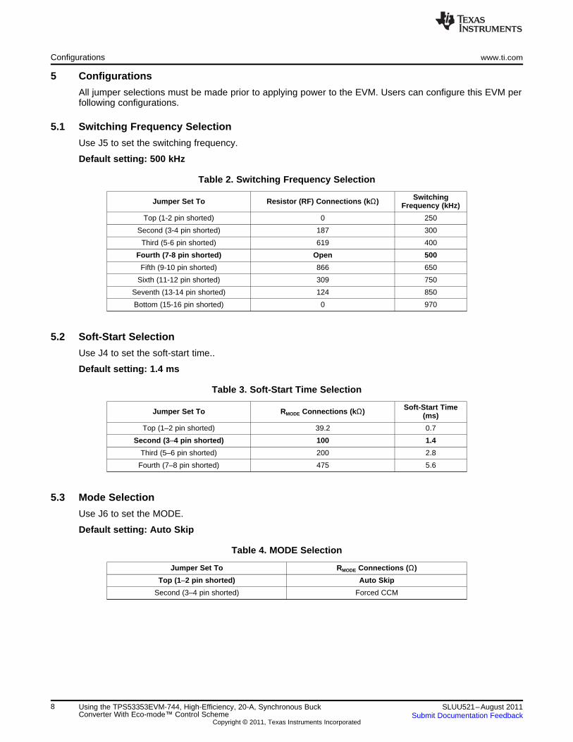
5 Configurations ............................................................................................................... 85.1 Switching Frequency Selection .................................................................................. 85.2 Soft-Start Selection ................................................................................................ 85.3 Mode Selection ..................................................................................................... 85.4 Enable Selection ................................................................................................... 9
6 Test Procedure .............................................................................................................. 96.1 Line/Load Regulation and Efficiency Measurement Procedure .............................................. 96.2 Control Loop Gain and Phase Measurement Procedure ..................................................... 96.3 Test Point List ..................................................................................................... 106.4 Equipment Shutdown ............................................................................................ 10
7 Performance Data and Typical Characteristic Curves ................................................................ 117.1 Efficiency .......................................................................................................... 117.2 Load Regulation .................................................................................................. 117.3 Load Regulation .................................................................................................. 127.4 Enable Turnon/ Turnoff .......................................................................................... 127.5 Output Ripple ..................................................................................................... 137.6 Switching Node ................................................................................................... 137.7 Output Transient With Auto-Skip Mode ........................................................................ 147.8 Output Transient With FCCM Mode ........................................................................... 147.9 Output 0.75-V Prebias Turnon .................................................................................. 157.10 Output Overcurrent and Short-Circuit Protection ............................................................. 157.11 Bode Plot .......................................................................................................... 167.12 Thermal Image .................................................................................................... 17
8 EVM Assembly Drawing and PCB Layout ............................................................................. 189 Bill of Materials ............................................................................................................. 22
List of Figures
1 TPS53353EVM-744 Schematic ........................................................................................... 5
2 Tip and Barrel Measurement for Vout Ripple ........................................................................... 6
Eco-mode, D-CAP are trademarks of Texas Instruments.
1SLUU521–August 2011 Using the TPS53353EVM-744, High-Efficiency, 20-A, Synchronous BuckConverter With Eco-mode™ Control SchemeSubmit Documentation Feedback
Copyright © 2011, Texas Instruments Incorporated
www.ti.com
3 TPS53353EVM-744 Recommended Test Setup ....................................................................... 7
4 Efficiency ................................................................................................................... 11
5 Load Regulation ........................................................................................................... 11
6 Line Regulation ............................................................................................................ 12
7 Enable Turnon ............................................................................................................. 12
8 Enable Turnoff ............................................................................................................. 12
9 Output Ripple .............................................................................................................. 13
10 Switching Node ............................................................................................................ 13
11 Output Transient From DCM to CCM................................................................................... 14
12 Output Transient From CCM to DCM................................................................................... 14
13 Output Transient With FCCM Mode .................................................................................... 14
14 Output 0.75-V Prebias Turnon........................................................................................... 15
15 Output Overcurrent Protection ........................................................................................... 15
16 Output Short Circuit ....................................................................................................... 15
17 Bode Plot at 12 VIN, 1.5 V/20 A .......................................................................................... 16
18 Top Board at 12 VIN, 1.5 V/20 A, 25°C Ambient Temperature Without Airflow.................................... 17
19 TPS53353EVM-744 Top Layer Assembly Drawing................................................................... 18
20 TPS53353EVM-744 Bottom Assembly Drawing ...................................................................... 18
21 TPS53353EVM-744 Top Copper ....................................................................................... 19
22 TPS53353EVM-744 Layer-2 Copper ................................................................................... 19
23 TPS53353EVM-744 Layer-3 Copper ................................................................................... 20
24 TPS53353EVM-744 Layer-4 Copper ................................................................................... 20
25 TPS53353EVM-744 Layer-5 Copper ................................................................................... 21
26 TPS53353EVM-744 Bottom Layer Copper ............................................................................ 21
List of Tables
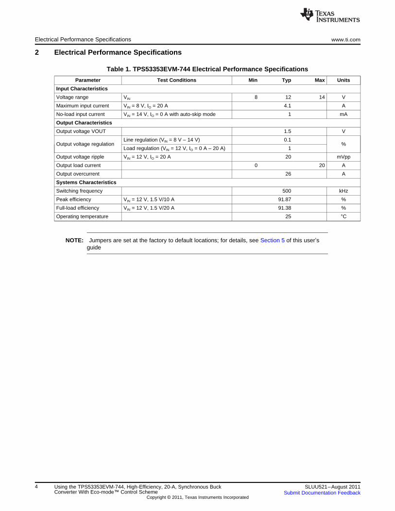
1 TPS53353EVM-744 Electrical Performance Specifications ........................................................... 4
2 Switching Frequency Selection ........................................................................................... 8
3 Soft-Start Time Selection .................................................................................................. 8
4 MODE Selection ............................................................................................................ 8
5 Enable Selection ............................................................................................................ 9
6 Test Point Functions ..................................................................................................... 10
7 TPS53353EVM-744 Bill of Materials.................................................................................... 22
2 Using the TPS53353EVM-744, High-Efficiency, 20-A, Synchronous Buck SLUU521–August 2011Converter With Eco-mode™ Control Scheme Submit Documentation Feedback
Copyright © 2011, Texas Instruments Incorporated
www.ti.com Description
1 Description
The TPS53353EVM-744 is designed to use a regulated 12-V bus to produce a regulated 1.5-V output atup to 20 A of load current. The TPS53353EVM-744 is designed to demonstrate the TPS53353 in a typicallow-voltage application while providing a number of test points to evaluate the performance of theTPS53353.
1.1 Typical Application• Server/storage
• Workstations and desktops
• Telecommunication infrastructure
1.2 Features
The TPS53353EVM-744 features:
• 20-Adc, steady-state output current
• Support prebias output voltage start-up
• J5 for selectable switching frequency setting
• J4 for selectable soft-start time
• J2 for enable function
• J6 for auto-skip and forced CCM selection
• Convenient test points for probing critical waveforms
3SLUU521–August 2011 Using the TPS53353EVM-744, High-Efficiency, 20-A, Synchronous BuckConverter With Eco-mode™ Control SchemeSubmit Documentation Feedback
Copyright © 2011, Texas Instruments Incorporated
Electrical Performance Specifications www.ti.com
2 Electrical Performance Specifications
Table 1. TPS53353EVM-744 Electrical Performance Specifications
Parameter Test Conditions Min Typ Max Units
Input Characteristics
Voltage range VIN 8 12 14 V
Maximum input current VIN = 8 V, IO = 20 A 4.1 A
No-load input current VIN = 14 V, IO = 0 A with auto-skip mode 1 mA
Output Characteristics
Output voltage VOUT 1.5 V
Line regulation (VIN = 8 V – 14 V) 0.1Output voltage regulation %
Load regulation (VIN = 12 V, IO = 0 A – 20 A) 1
Output voltage ripple VIN = 12 V, IO = 20 A 20 mVpp
Output load current 0 20 A
Output overcurrent 26 A
Systems Characteristics
Switching frequency 500 kHz
Peak efficiency VIN = 12 V, 1.5 V/10 A 91.87 %
Full-load efficiency VIN = 12 V, 1.5 V/20 A 91.38 %
Operating temperature 25 °C
NOTE: Jumpers are set at the factory to default locations; for details, see Section 5 of this user’sguide
4 Using the TPS53353EVM-744, High-Efficiency, 20-A, Synchronous Buck SLUU521–August 2011Converter With Eco-mode™ Control Scheme Submit Documentation Feedback
Copyright © 2011, Texas Instruments Incorporated
www.ti.com Schematic
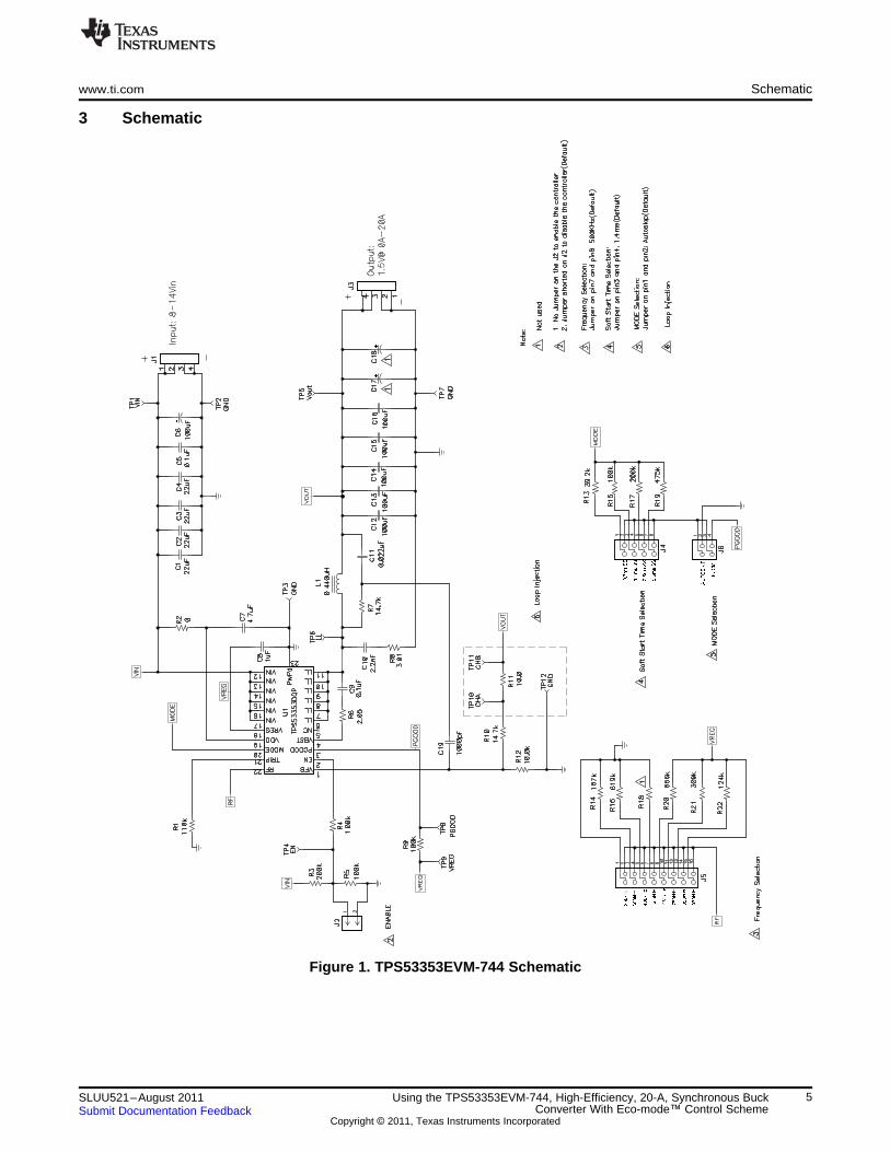
3 Schematic
Figure 1. TPS53353EVM-744 Schematic
5SLUU521–August 2011 Using the TPS53353EVM-744, High-Efficiency, 20-A, Synchronous BuckConverter With Eco-mode™ Control SchemeSubmit Documentation Feedback
Copyright © 2011, Texas Instruments Incorporated
Test Setup www.ti.com
4 Test Setup
4.1 Test Equipment
Voltage Source: The input voltage source Vin must be a 0-V to 14-V variable dc source capable ofsupplying 10 Adc. Connect VIN to J1 as shown in Figure 3.
Multimeters:• V1: VIN at TP1 (VIN) and TP2 (GND).
• V2: VOUT at TP5 (VOUT) and TP7 (GND).
• A1: VIN input current
Output Load: The output load should be an electronic constant resistance mode load capable of0-30ADC at 1.5V.
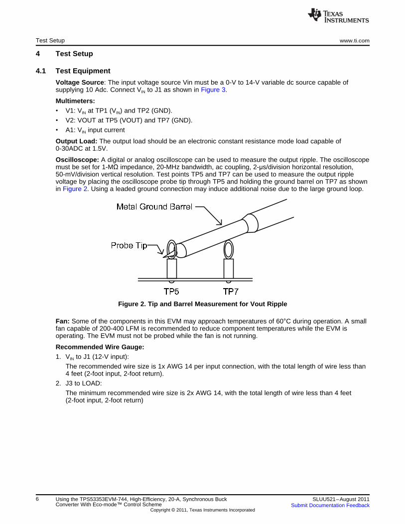
Oscilloscope: A digital or analog oscilloscope can be used to measure the output ripple. The oscilloscopemust be set for 1-MΩ impedance, 20-MHz bandwidth, ac coupling, 2-µs/division horizontal resolution,50-mV/division vertical resolution. Test points TP5 and TP7 can be used to measure the output ripplevoltage by placing the oscilloscope probe tip through TP5 and holding the ground barrel on TP7 as shownin Figure 2. Using a leaded ground connection may induce additional noise due to the large ground loop.
Figure 2. Tip and Barrel Measurement for Vout Ripple
Fan: Some of the components in this EVM may approach temperatures of 60°C during operation. A smallfan capable of 200-400 LFM is recommended to reduce component temperatures while the EVM isoperating. The EVM must not be probed while the fan is not running.
Recommended Wire Gauge:1. VIN to J1 (12-V input):
The recommended wire size is 1x AWG 14 per input connection, with the total length of wire less than4 feet (2-foot input, 2-foot return).
2. J3 to LOAD:
The minimum recommended wire size is 2x AWG 14, with the total length of wire less than 4 feet(2-foot input, 2-foot return)
6 Using the TPS53353EVM-744, High-Efficiency, 20-A, Synchronous Buck SLUU521–August 2011Converter With Eco-mode™ Control Scheme Submit Documentation Feedback
Copyright © 2011, Texas Instruments Incorporated
www.ti.com Test Setup
4.2 Recommended Test Setup
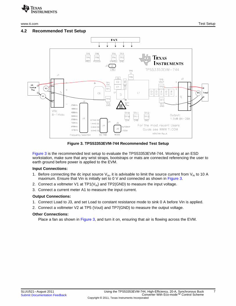
Figure 3. TPS53353EVM-744 Recommended Test Setup
Figure 3 is the recommended test setup to evaluate the TPS53353EVM-744. Working at an ESDworkstation, make sure that any wrist straps, bootstraps or mats are connected referencing the user toearth ground before power is applied to the EVM.
Input Connections:1. Before connecting the dc input source VIN, it is advisable to limit the source current from VIN to 10 A
maximum. Ensure that Vin is initially set to 0 V and connected as shown in Figure 3.
2. Connect a voltmeter V1 at TP1(VIN) and TP2(GND) to measure the input voltage.
3. Connect a current meter A1 to measure the input current.
Output Connections:1. Connect Load to J3, and set Load to constant resistance mode to sink 0 A before Vin is applied.
2. Connect a voltmeter V2 at TP5 (Vout) and TP7(GND) to measure the output voltage.
Other Connections:Place a fan as shown in Figure 3, and turn it on, ensuring that air is flowing across the EVM.
7SLUU521–August 2011 Using the TPS53353EVM-744, High-Efficiency, 20-A, Synchronous BuckConverter With Eco-mode™ Control SchemeSubmit Documentation Feedback
Copyright © 2011, Texas Instruments Incorporated
Configurations www.ti.com
5 Configurations
All jumper selections must be made prior to applying power to the EVM. Users can configure this EVM perfollowing configurations.
5.1 Switching Frequency Selection
Use J5 to set the switching frequency.
Default setting: 500 kHz
Table 2. Switching Frequency Selection
SwitchingJumper Set To Resistor (RF) Connections (kΩ) Frequency (kHz)
Top (1-2 pin shorted) 0 250
Second (3-4 pin shorted) 187 300
Third (5-6 pin shorted) 619 400
Fourth (7-8 pin shorted) Open 500
Fifth (9-10 pin shorted) 866 650
Sixth (11-12 pin shorted) 309 750
Seventh (13-14 pin shorted) 124 850
Bottom (15-16 pin shorted) 0 970
5.2 Soft-Start Selection
Use J4 to set the soft-start time..
Default setting: 1.4 ms
Table 3. Soft-Start Time Selection
Soft-Start TimeJumper Set To RMODE Connections (kΩ) (ms)
Top (1–2 pin shorted) 39.2 0.7
Second (3–4 pin shorted) 100 1.4
Third (5–6 pin shorted) 200 2.8
Fourth (7–8 pin shorted) 475 5.6
5.3 Mode Selection
Use J6 to set the MODE.
Default setting: Auto Skip
Table 4. MODE Selection
Jumper Set To RMODE Connections (Ω)
Top (1–2 pin shorted) Auto Skip
Second (3–4 pin shorted) Forced CCM
8 Using the TPS53353EVM-744, High-Efficiency, 20-A, Synchronous Buck SLUU521–August 2011Converter With Eco-mode™ Control Scheme Submit Documentation Feedback
Copyright © 2011, Texas Instruments Incorporated
www.ti.com Test Procedure
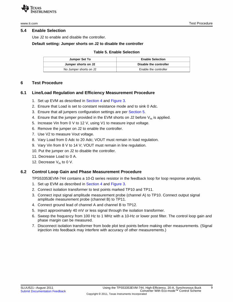
5.4 Enable Selection
Use J2 to enable and disable the controller.
Default setting: Jumper shorts on J2 to disable the controller
Table 5. Enable Selection
Jumper Set To Enable Selection
Jumper shorts on J2 Disable the controller
No Jumper shorts on J2 Enable the controller
6 Test Procedure
6.1 Line/Load Regulation and Efficiency Measurement Procedure
1. Set up EVM as described in Section 4 and Figure 3.
2. Ensure that Load is set to constant resistance mode and to sink 0 Adc.
3. Ensure that all jumpers configuration settings are per Section 5.
4. Ensure that the jumper provided in the EVM shorts on J2 before VIN is applied.
5. Increase Vin from 0 V to 12 V, using V1 to measure input voltage.
6. Remove the jumper on J2 to enable the controller.
7. Use V2 to measure Vout voltage.
8. Vary Load from 0 Adc to 20 Adc; VOUT must remain in load regulation.
9. Vary Vin from 8 V to 14 V; VOUT must remain in line regulation.
10. Put the jumper on J2 to disable the controller.
11. Decrease Load to 0 A.
12. Decrease VIN to 0 V.
6.2 Control Loop Gain and Phase Measurement Procedure
TPS53353EVM-744 contains a 10-Ω series resistor in the feedback loop for loop response analysis.
1. Set up EVM as described in Section 4 and Figure 3.
2. Connect isolation transformer to test points marked TP10 and TP11.
3. Connect input signal amplitude measurement probe (channel A) to TP10. Connect output signalamplitude measurement probe (channel B) to TP11.
4. Connect ground lead of channel A and channel B to TP12.
5. Inject approximately 40 mV or less signal through the isolation transformer.
6. Sweep the frequency from 100 Hz to 1 MHz with a 10-Hz or lower post filter. The control loop gain andphase margin can be measured.
7. Disconnect isolation transformer from bode plot test points before making other measurements. (Signalinjection into feedback may interfere with accuracy of other measurements.)
9SLUU521–August 2011 Using the TPS53353EVM-744, High-Efficiency, 20-A, Synchronous BuckConverter With Eco-mode™ Control SchemeSubmit Documentation Feedback
Copyright © 2011, Texas Instruments Incorporated
Test Procedure www.ti.com
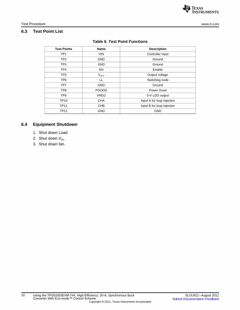
6.3 Test Point List
Table 6. Test Point Functions
Test Points Name Description
TP1 VIN Controller input
TP2 GND Ground
TP3 GND Ground
TP4 EN Enable
TP5 VOUT Output voltage
TP6 LL Switching node
TP7 GND Ground
TP8 PGOOD Power Good
TP9 VREG 5-V LDO output
TP10 CHA Input A for loop injection
TP11 CHB Input B for loop injection
TP12 GND GND
6.4 Equipment Shutdown
1. Shut down Load.
2. Shut down VIN.
3. Shut down fan.
10 Using the TPS53353EVM-744, High-Efficiency, 20-A, Synchronous Buck SLUU521–August 2011Converter With Eco-mode™ Control Scheme Submit Documentation Feedback
Copyright © 2011, Texas Instruments Incorporated
0
10
20
30
40
50
60
70
80
90
100
0.001 0.01 0.1 1 10 100Output Current (A)
Effi
cien
cy (
%)
VIN = 8 V, Auto SkipVIN = 12 V, Auto SkipVIN = 14 V, Auto SkipVIN = 8 V, FCCMVIN = 12 V, FCCMVIN = 14 V, FCCM
f = 500 kHzVOUT = 1.5 V
G001
1.47
1.48
1.49
1.50
1.51
1.52
1.53
0 5 10 15 20Output Current (A)
Out
put V
olta
ge (
V)
VIN = 8 V, Auto SkipVIN = 12 V, Auto SkipVIN = 14 V, Auto SkipVIN = 8 V, FCCMVIN = 12 V, FCCMVIN = 14 V, FCCM
f = 500 kHz
G002
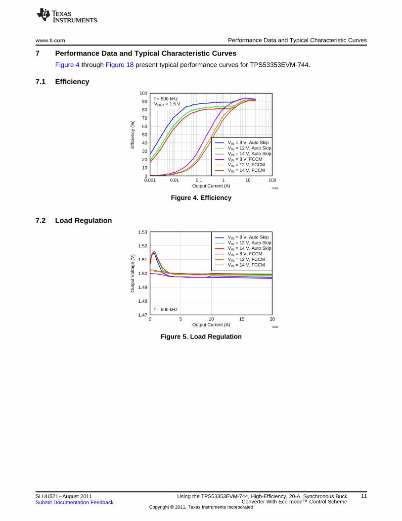
www.ti.com Performance Data and Typical Characteristic Curves
7 Performance Data and Typical Characteristic Curves
Figure 4 through Figure 18 present typical performance curves for TPS53353EVM-744.
7.1 Efficiency
Figure 4. Efficiency
7.2 Load Regulation
Figure 5. Load Regulation
11SLUU521–August 2011 Using the TPS53353EVM-744, High-Efficiency, 20-A, Synchronous BuckConverter With Eco-mode™ Control SchemeSubmit Documentation Feedback
Copyright © 2011, Texas Instruments Incorporated
1.47
1.48
1.49
1.50
1.51
1.52
1.53
8 9 10 11 12 13 14Input Voltage (V)
Out
put V
olta
ge (
V)
IOUT = 0 A, Auto SkipIOUT = 0 A, FCCMIOUT = 20 A
f = 500 kHz
G003
Performance Data and Typical Characteristic Curves www.ti.com
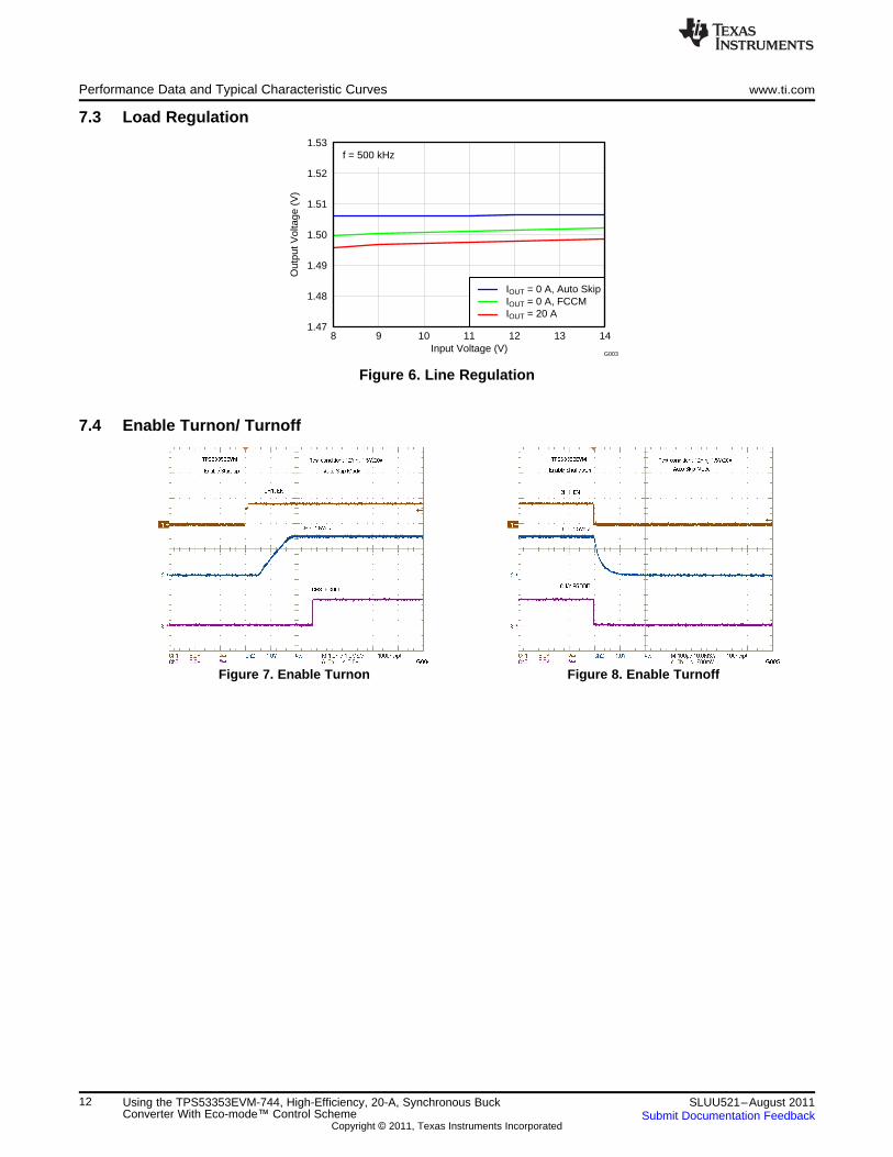
7.3 Load Regulation
Figure 6. Line Regulation
7.4 Enable Turnon/ Turnoff
Figure 7. Enable Turnon Figure 8. Enable Turnoff
12 Using the TPS53353EVM-744, High-Efficiency, 20-A, Synchronous Buck SLUU521–August 2011Converter With Eco-mode™ Control Scheme Submit Documentation Feedback
Copyright © 2011, Texas Instruments Incorporated
www.ti.com Performance Data and Typical Characteristic Curves
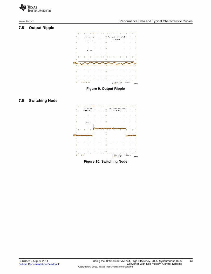
7.5 Output Ripple
Figure 9. Output Ripple
7.6 Switching Node
Figure 10. Switching Node
13SLUU521–August 2011 Using the TPS53353EVM-744, High-Efficiency, 20-A, Synchronous BuckConverter With Eco-mode™ Control SchemeSubmit Documentation Feedback
Copyright © 2011, Texas Instruments Incorporated
Performance Data and Typical Characteristic Curves www.ti.com
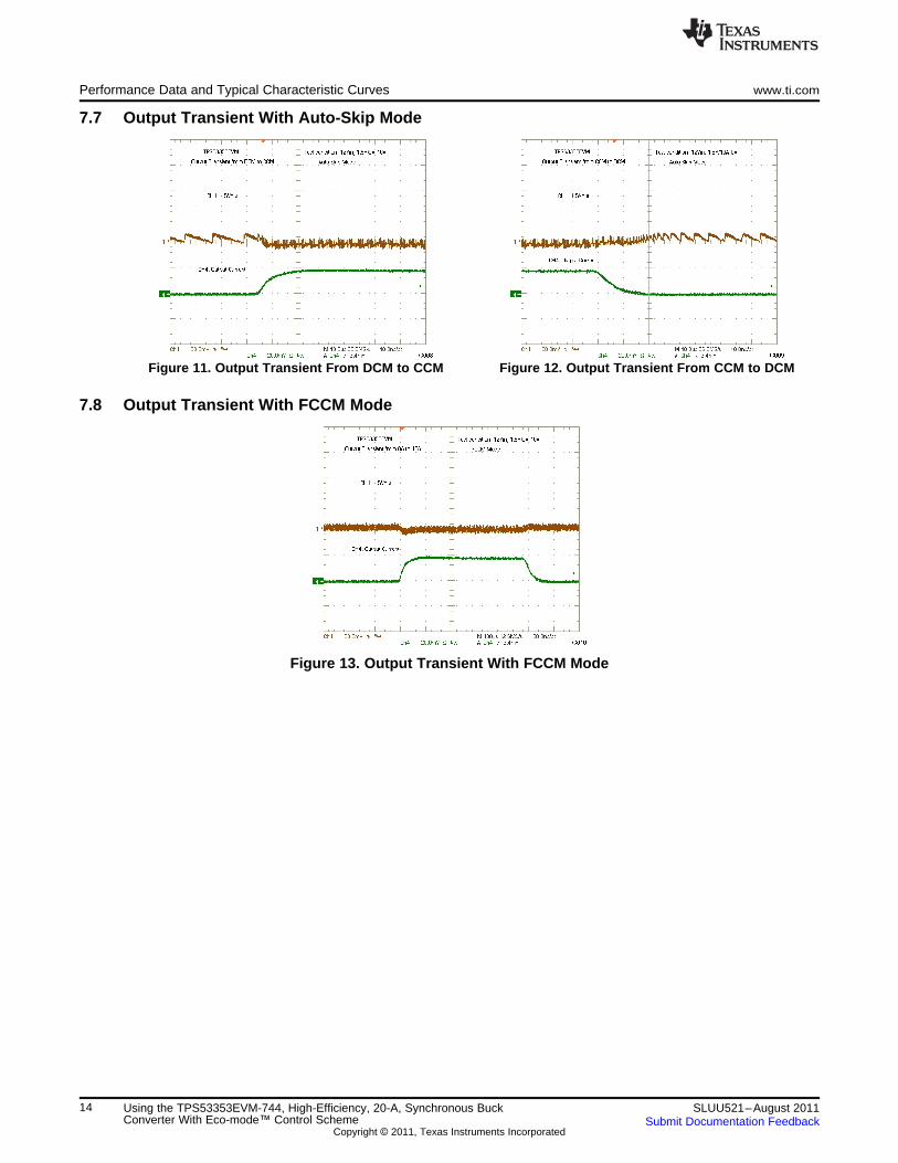
7.7 Output Transient With Auto-Skip Mode
Figure 11. Output Transient From DCM to CCM Figure 12. Output Transient From CCM to DCM
7.8 Output Transient With FCCM Mode
Figure 13. Output Transient With FCCM Mode
14 Using the TPS53353EVM-744, High-Efficiency, 20-A, Synchronous Buck SLUU521–August 2011Converter With Eco-mode™ Control Scheme Submit Documentation Feedback
Copyright © 2011, Texas Instruments Incorporated
TPS53355EVM
Over Current ProtectionTest Condition: 12 Vin OCP
Ch1: 1.5 Vout
Ch2: LL
Ch3: PGOOD
TPS53355EVM
Over Current Protection
Ch1: 1.5 Vout
Ch2: LL
Ch3: PGOOD
Test Condition: 12 Vin,
1.5 V Short Circuit
www.ti.com Performance Data and Typical Characteristic Curves
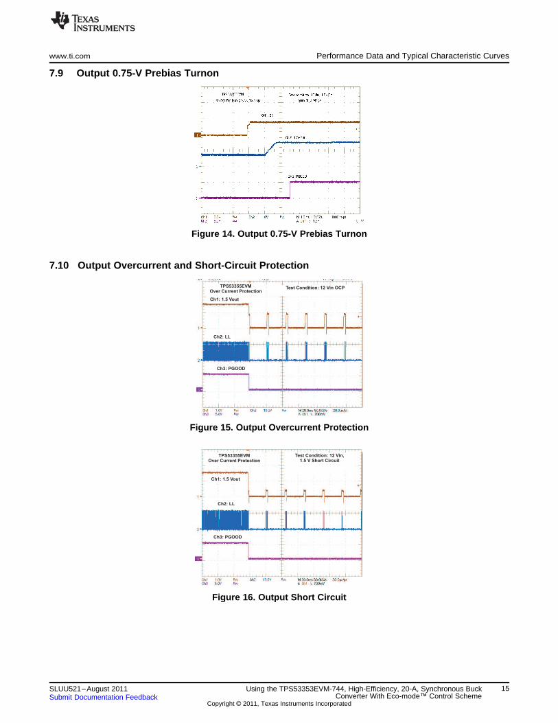
7.9 Output 0.75-V Prebias Turnon
Figure 14. Output 0.75-V Prebias Turnon
7.10 Output Overcurrent and Short-Circuit Protection
Figure 15. Output Overcurrent Protection
Figure 16. Output Short Circuit
15SLUU521–August 2011 Using the TPS53353EVM-744, High-Efficiency, 20-A, Synchronous BuckConverter With Eco-mode™ Control SchemeSubmit Documentation Feedback
Copyright © 2011, Texas Instruments Incorporated
Performance Data and Typical Characteristic Curves www.ti.com
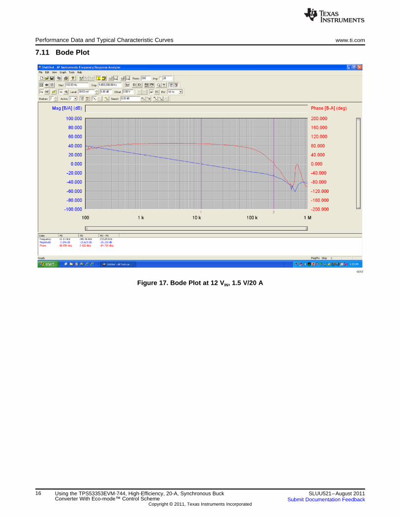
7.11 Bode Plot
Figure 17. Bode Plot at 12 VIN, 1.5 V/20 A
16 Using the TPS53353EVM-744, High-Efficiency, 20-A, Synchronous Buck SLUU521–August 2011Converter With Eco-mode™ Control Scheme Submit Documentation Feedback
Copyright © 2011, Texas Instruments Incorporated
www.ti.com Performance Data and Typical Characteristic Curves
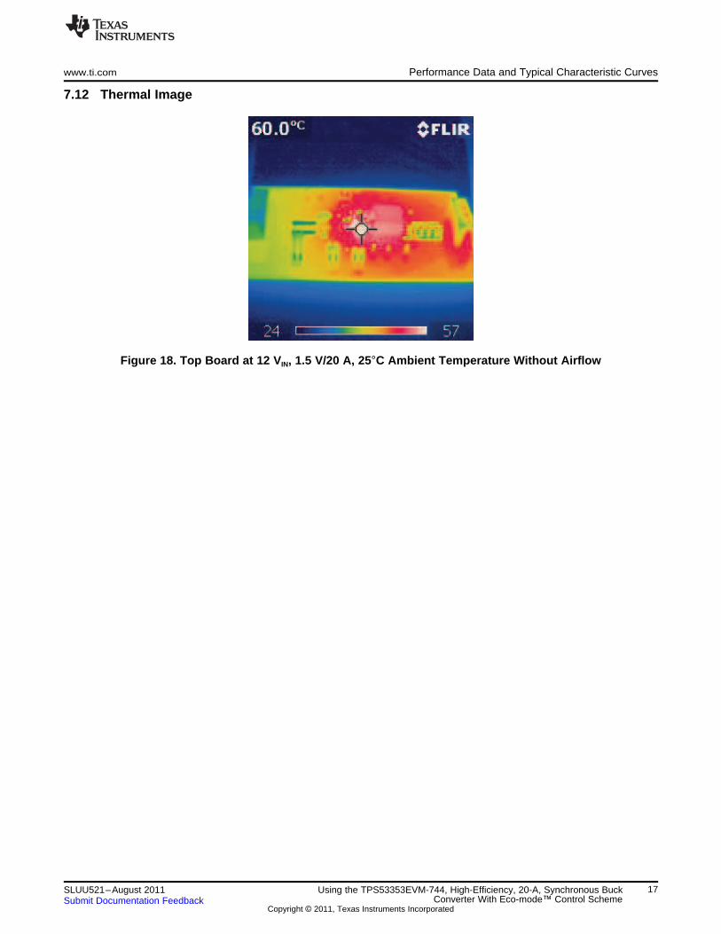
7.12 Thermal Image
Figure 18. Top Board at 12 VIN, 1.5 V/20 A, 25°C Ambient Temperature Without Airflow
17SLUU521–August 2011 Using the TPS53353EVM-744, High-Efficiency, 20-A, Synchronous BuckConverter With Eco-mode™ Control SchemeSubmit Documentation Feedback
Copyright © 2011, Texas Instruments Incorporated
EVM Assembly Drawing and PCB Layout www.ti.com
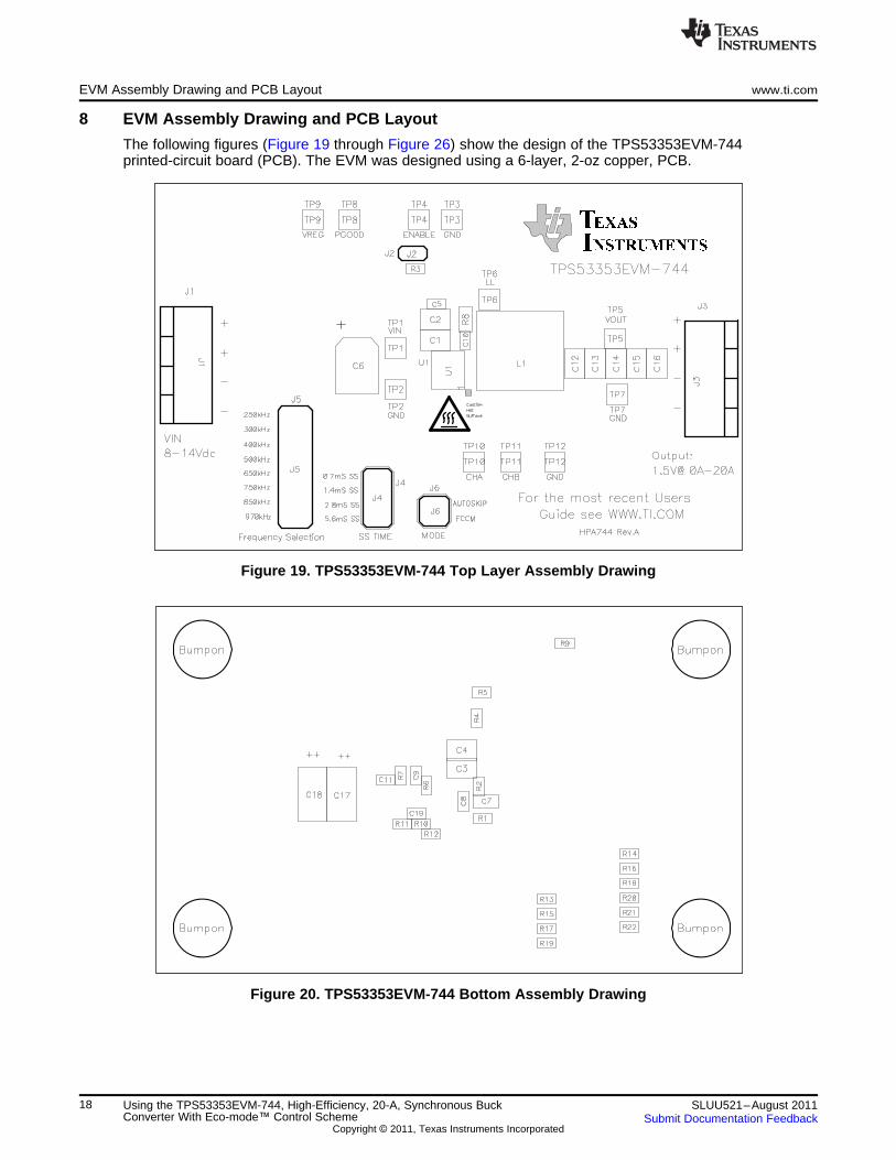
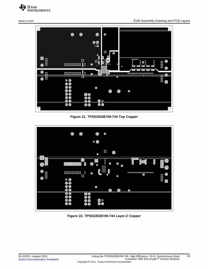
8 EVM Assembly Drawing and PCB Layout
The following figures (Figure 19 through Figure 26) show the design of the TPS53353EVM-744printed-circuit board (PCB). The EVM was designed using a 6-layer, 2-oz copper, PCB.
Figure 19. TPS53353EVM-744 Top Layer Assembly Drawing
Figure 20. TPS53353EVM-744 Bottom Assembly Drawing
18 Using the TPS53353EVM-744, High-Efficiency, 20-A, Synchronous Buck SLUU521–August 2011Converter With Eco-mode™ Control Scheme Submit Documentation Feedback
Copyright © 2011, Texas Instruments Incorporated
www.ti.com EVM Assembly Drawing and PCB Layout
Figure 21. TPS53353EVM-744 Top Copper
Figure 22. TPS53353EVM-744 Layer-2 Copper
19SLUU521–August 2011 Using the TPS53353EVM-744, High-Efficiency, 20-A, Synchronous BuckConverter With Eco-mode™ Control SchemeSubmit Documentation Feedback
Copyright © 2011, Texas Instruments Incorporated
EVM Assembly Drawing and PCB Layout www.ti.com
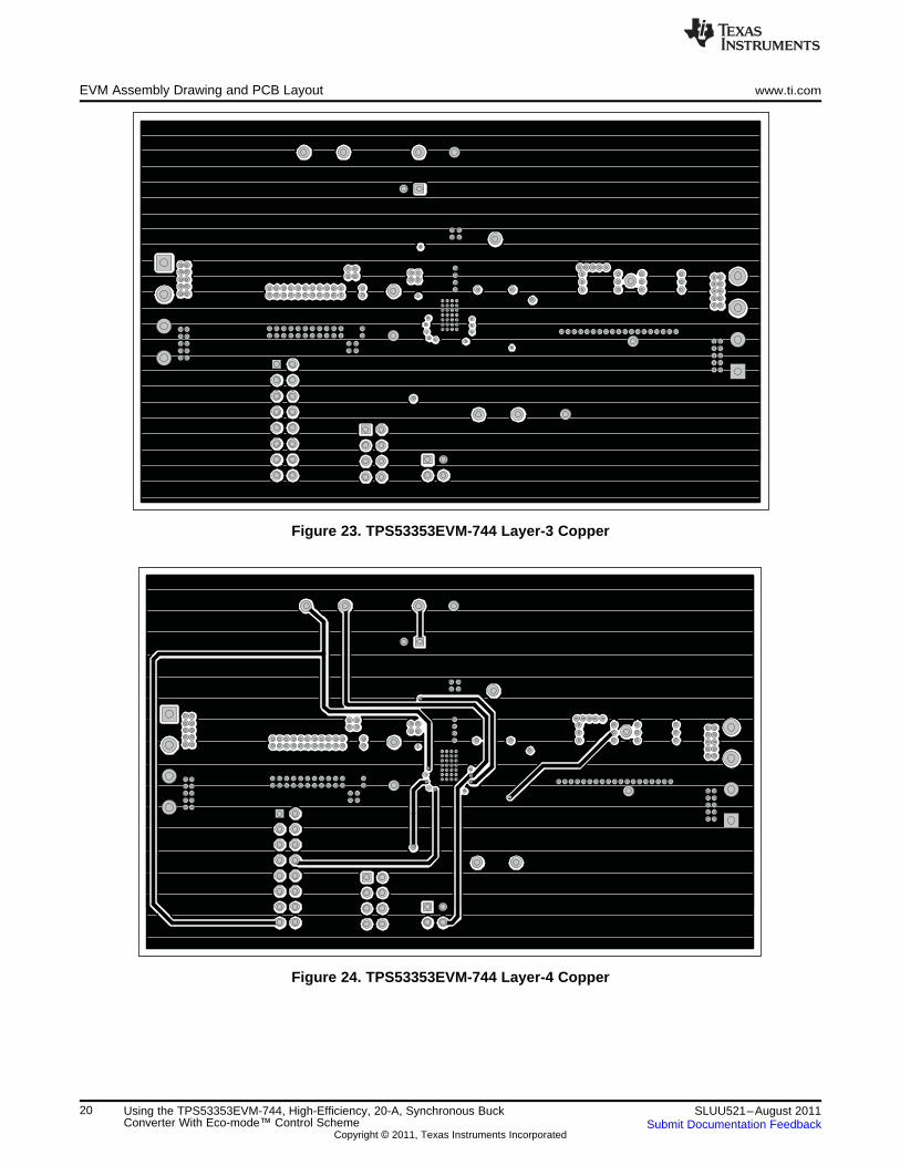
Figure 23. TPS53353EVM-744 Layer-3 Copper
Figure 24. TPS53353EVM-744 Layer-4 Copper
20 Using the TPS53353EVM-744, High-Efficiency, 20-A, Synchronous Buck SLUU521–August 2011Converter With Eco-mode™ Control Scheme Submit Documentation Feedback
Copyright © 2011, Texas Instruments Incorporated
www.ti.com EVM Assembly Drawing and PCB Layout
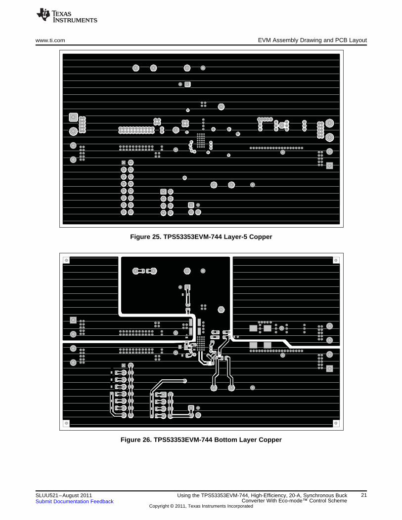
Figure 25. TPS53353EVM-744 Layer-5 Copper
Figure 26. TPS53353EVM-744 Bottom Layer Copper
21SLUU521–August 2011 Using the TPS53353EVM-744, High-Efficiency, 20-A, Synchronous BuckConverter With Eco-mode™ Control SchemeSubmit Documentation Feedback
Copyright © 2011, Texas Instruments Incorporated
Bill of Materials www.ti.com
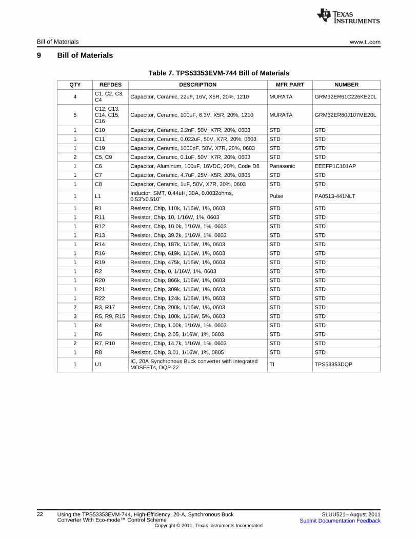
9 Bill of Materials
Table 7. TPS53353EVM-744 Bill of Materials
QTY REFDES DESCRIPTION MFR PART NUMBER
C1, C2, C3,4 Capacitor, Ceramic, 22uF, 16V, X5R, 20%, 1210 MURATA GRM32ER61C226KE20LC4
C12, C13,5 C14, C15, Capacitor, Ceramic, 100uF, 6.3V, X5R, 20%, 1210 MURATA GRM32ER60J107ME20L
C16
1 C10 Capacitor, Ceramic, 2.2nF, 50V, X7R, 20%, 0603 STD STD
1 C11 Capacitor, Ceramic, 0.022uF, 50V, X7R, 20%, 0603 STD STD
1 C19 Capacitor, Ceramic, 1000pF, 50V, X7R, 20%, 0603 STD STD
2 C5, C9 Capacitor, Ceramic, 0.1uF, 50V, X7R, 20%, 0603 STD STD
1 C6 Capacitor, Aluminum, 100uF, 16VDC, 20%, Code D8 Panasonic EEEFP1C101AP
1 C7 Capacitor, Ceramic, 4.7uF, 25V, X5R, 20%, 0805 STD STD
1 C8 Capacitor, Ceramic, 1uF, 50V, X7R, 20%, 0603 STD STD
Inductor, SMT, 0.44uH, 30A, 0.0032ohms,1 L1 Pulse PA0513-441NLT0.53”x0.510”1 R1 Resistor, Chip, 110k, 1/16W, 1%, 0603 STD STD
1 R11 Resistor, Chip, 10, 1/16W, 1%, 0603 STD STD
1 R12 Resistor, Chip, 10.0k, 1/16W, 1%, 0603 STD STD
1 R13 Resistor, Chip, 39.2k, 1/16W, 1%, 0603 STD STD
1 R14 Resistor, Chip, 187k, 1/16W, 1%, 0603 STD STD
1 R16 Resistor, Chip, 619k, 1/16W, 1%, 0603 STD STD
1 R19 Resistor, Chip, 475k, 1/16W, 1%, 0603 STD STD
1 R2 Resistor, Chip, 0, 1/16W, 1%, 0603 STD STD
1 R20 Resistor, Chip, 866k, 1/16W, 1%, 0603 STD STD
1 R21 Resistor, Chip, 309k, 1/16W, 1%, 0603 STD STD
1 R22 Resistor, Chip, 124k, 1/16W, 1%, 0603 STD STD
2 R3, R17 Resistor, Chip, 200k, 1/16W, 1%, 0603 STD STD
3 R5, R9, R15 Resistor, Chip, 100k, 1/16W, 5%, 0603 STD STD
1 R4 Resistor, Chip, 1.00k, 1/16W, 1%, 0603 STD STD
1 R6 Resistor, Chip, 2.05, 1/16W, 1%, 0603 STD STD
2 R7, R10 Resistor, Chip, 14.7k, 1/16W, 1%, 0603 STD STD
1 R8 Resistor, Chip, 3.01, 1/16W, 1%, 0805 STD STD
IC, 20A Synchronous Buck converter with integrated1 U1 TI TPS53353DQPMOSFETs, DQP-22
22 Using the TPS53353EVM-744, High-Efficiency, 20-A, Synchronous Buck SLUU521–August 2011Converter With Eco-mode™ Control Scheme Submit Documentation Feedback
Copyright © 2011, Texas Instruments Incorporated
Evaluation Board/Kit Important Notice
Texas Instruments (TI) provides the enclosed product(s) under the following conditions:
This evaluation board/kit is intended for use for ENGINEERING DEVELOPMENT, DEMONSTRATION, OR EVALUATIONPURPOSES ONLY and is not considered by TI to be a finished end-product fit for general consumer use. Persons handling theproduct(s) must have electronics training and observe good engineering practice standards. As such, the goods being provided arenot intended to be complete in terms of required design-, marketing-, and/or manufacturing-related protective considerations,including product safety and environmental measures typically found in end products that incorporate such semiconductorcomponents or circuit boards. This evaluation board/kit does not fall within the scope of the European Union directives regardingelectromagnetic compatibility, restricted substances (RoHS), recycling (WEEE), FCC, CE or UL, and therefore may not meet thetechnical requirements of these directives or other related directives.
Should this evaluation board/kit not meet the specifications indicated in the User’s Guide, the board/kit may be returned within 30days from the date of delivery for a full refund. THE FOREGOING WARRANTY IS THE EXCLUSIVE WARRANTY MADE BYSELLER TO BUYER AND IS IN LIEU OF ALL OTHER WARRANTIES, EXPRESSED, IMPLIED, OR STATUTORY, INCLUDINGANY WARRANTY OF MERCHANTABILITY OR FITNESS FOR ANY PARTICULAR PURPOSE.
The user assumes all responsibility and liability for proper and safe handling of the goods. Further, the user indemnifies TI from allclaims arising from the handling or use of the goods. Due to the open construction of the product, it is the user’s responsibility totake any and all appropriate precautions with regard to electrostatic discharge.
EXCEPT TO THE EXTENT OF THE INDEMNITY SET FORTH ABOVE, NEITHER PARTY SHALL BE LIABLE TO THE OTHERFOR ANY INDIRECT, SPECIAL, INCIDENTAL, OR CONSEQUENTIAL DAMAGES.
TI currently deals with a variety of customers for products, and therefore our arrangement with the user is not exclusive.
TI assumes no liability for applications assistance, customer product design, software performance, or infringement ofpatents or services described herein.
Please read the User’s Guide and, specifically, the Warnings and Restrictions notice in the User’s Guide prior to handling theproduct. This notice contains important safety information about temperatures and voltages. For additional information on TI’senvironmental and/or safety programs, please contact the TI application engineer or visit www.ti.com/esh.
No license is granted under any patent right or other intellectual property right of TI covering or relating to any machine, process, orcombination in which such TI products or services might be or are used.
FCC Warning
This evaluation board/kit is intended for use for ENGINEERING DEVELOPMENT, DEMONSTRATION, OR EVALUATIONPURPOSES ONLY and is not considered by TI to be a finished end-product fit for general consumer use. It generates, uses, andcan radiate radio frequency energy and has not been tested for compliance with the limits of computing devices pursuant to part 15of FCC rules, which are designed to provide reasonable protection against radio frequency interference. Operation of thisequipment in other environments may cause interference with radio communications, in which case the user at his own expensewill be required to take whatever measures may be required to correct this interference.
EVM Warnings and Restrictions
It is important to operate this EVM within the input voltage range of 8 V to 14 V and the output voltage range of 0.6 V to 5.5 V .
Exceeding the specified input range may cause unexpected operation and/or irreversible damage to the EVM. If there arequestions concerning the input range, please contact a TI field representative prior to connecting the input power.
Applying loads outside of the specified output range may result in unintended operation and/or possible permanent damage to theEVM. Please consult the EVM User's Guide prior to connecting any load to the EVM output. If there is uncertainty as to the loadspecification, please contact a TI field representative.
During normal operation, some circuit components may have case temperatures greater than 60°C. The EVM is designed tooperate properly with certain components above 60°C as long as the input and output ranges are maintained. These componentsinclude but are not limited to linear regulators, switching transistors, pass transistors, and current sense resistors. These types ofdevices can be identified using the EVM schematic located in the EVM User's Guide. When placing measurement probes nearthese devices during operation, please be aware that these devices may be very warm to the touch.
Mailing Address: Texas Instruments, Post Office Box 655303, Dallas, Texas 75265Copyright © 2011, Texas Instruments Incorporated
EVALUATION BOARD/KIT/MODULE (EVM) ADDITIONAL TERMSTexas Instruments (TI) provides the enclosed Evaluation Board/Kit/Module (EVM) under the following conditions:
The user assumes all responsibility and liability for proper and safe handling of the goods. Further, the user indemnifies TI from all claimsarising from the handling or use of the goods.
Should this evaluation board/kit not meet the specifications indicated in the User’s Guide, the board/kit may be returned within 30 days fromthe date of delivery for a full refund. THE FOREGOING LIMITED WARRANTY IS THE EXCLUSIVE WARRANTY MADE BY SELLER TOBUYER AND IS IN LIEU OF ALL OTHER WARRANTIES, EXPRESSED, IMPLIED, OR STATUTORY, INCLUDING ANY WARRANTY OFMERCHANTABILITY OR FITNESS FOR ANY PARTICULAR PURPOSE. EXCEPT TO THE EXTENT OF THE INDEMNITY SET FORTHABOVE, NEITHER PARTY SHALL BE LIABLE TO THE OTHER FOR ANY INDIRECT, SPECIAL, INCIDENTAL, OR CONSEQUENTIALDAMAGES.
Please read the User's Guide and, specifically, the Warnings and Restrictions notice in the User's Guide prior to handling the product. Thisnotice contains important safety information about temperatures and voltages. For additional information on TI's environmental and/or safetyprograms, please visit www.ti.com/esh or contact TI.
No license is granted under any patent right or other intellectual property right of TI covering or relating to any machine, process, orcombination in which such TI products or services might be or are used. TI currently deals with a variety of customers for products, andtherefore our arrangement with the user is not exclusive. TI assumes no liability for applications assistance, customer product design,software performance, or infringement of patents or services described herein.
REGULATORY COMPLIANCE INFORMATIONAs noted in the EVM User’s Guide and/or EVM itself, this EVM and/or accompanying hardware may or may not be subject to the FederalCommunications Commission (FCC) and Industry Canada (IC) rules.
For EVMs not subject to the above rules, this evaluation board/kit/module is intended for use for ENGINEERING DEVELOPMENT,DEMONSTRATION OR EVALUATION PURPOSES ONLY and is not considered by TI to be a finished end product fit for general consumeruse. It generates, uses, and can radiate radio frequency energy and has not been tested for compliance with the limits of computingdevices pursuant to part 15 of FCC or ICES-003 rules, which are designed to provide reasonable protection against radio frequencyinterference. Operation of the equipment may cause interference with radio communications, in which case the user at his own expense willbe required to take whatever measures may be required to correct this interference.
General Statement for EVMs including a radioUser Power/Frequency Use Obligations: This radio is intended for development/professional use only in legally allocated frequency andpower limits. Any use of radio frequencies and/or power availability of this EVM and its development application(s) must comply with locallaws governing radio spectrum allocation and power limits for this evaluation module. It is the user’s sole responsibility to only operate thisradio in legally acceptable frequency space and within legally mandated power limitations. Any exceptions to this are strictly prohibited andunauthorized by Texas Instruments unless user has obtained appropriate experimental/development licenses from local regulatoryauthorities, which is responsibility of user including its acceptable authorization.
For EVMs annotated as FCC – FEDERAL COMMUNICATIONS COMMISSION Part 15 Compliant
CautionThis device complies with part 15 of the FCC Rules. Operation is subject to the following two conditions: (1) This device may not causeharmful interference, and (2) this device must accept any interference received, including interference that may cause undesired operation.
Changes or modifications not expressly approved by the party responsible for compliance could void the user's authority to operate theequipment.
FCC Interference Statement for Class A EVM devicesThis equipment has been tested and found to comply with the limits for a Class A digital device, pursuant to part 15 of the FCC Rules.These limits are designed to provide reasonable protection against harmful interference when the equipment is operated in a commercialenvironment. This equipment generates, uses, and can radiate radio frequency energy and, if not installed and used in accordance with theinstruction manual, may cause harmful interference to radio communications. Operation of this equipment in a residential area is likely tocause harmful interference in which case the user will be required to correct the interference at his own expense.
FCC Interference Statement for Class B EVM devicesThis equipment has been tested and found to comply with the limits for a Class B digital device, pursuant to part 15 of the FCC Rules.These limits are designed to provide reasonable protection against harmful interference in a residential installation. This equipmentgenerates, uses and can radiate radio frequency energy and, if not installed and used in accordance with the instructions, may causeharmful interference to radio communications. However, there is no guarantee that interference will not occur in a particular installation. Ifthis equipment does cause harmful interference to radio or television reception, which can be determined by turning the equipment off andon, the user is encouraged to try to correct the interference by one or more of the following measures:
• Reorient or relocate the receiving antenna.• Increase the separation between the equipment and receiver.• Connect the equipment into an outlet on a circuit different from that to which the receiver is connected.• Consult the dealer or an experienced radio/TV technician for help.
For EVMs annotated as IC – INDUSTRY CANADA Compliant
This Class A or B digital apparatus complies with Canadian ICES-003.
Changes or modifications not expressly approved by the party responsible for compliance could void the user’s authority to operate theequipment.
Concerning EVMs including radio transmitters
This device complies with Industry Canada licence-exempt RSS standard(s). Operation is subject to the following two conditions: (1) thisdevice may not cause interference, and (2) this device must accept any interference, including interference that may cause undesiredoperation of the device.
Concerning EVMs including detachable antennasUnder Industry Canada regulations, this radio transmitter may only operate using an antenna of a type and maximum (or lesser) gainapproved for the transmitter by Industry Canada. To reduce potential radio interference to other users, the antenna type and its gain shouldbe so chosen that the equivalent isotropically radiated power (e.i.r.p.) is not more than that necessary for successful communication.
This radio transmitter has been approved by Industry Canada to operate with the antenna types listed in the user guide with the maximumpermissible gain and required antenna impedance for each antenna type indicated. Antenna types not included in this list, having a gaingreater than the maximum gain indicated for that type, are strictly prohibited for use with this device.
Cet appareil numérique de la classe A ou B est conforme à la norme NMB-003 du Canada.
Les changements ou les modifications pas expressément approuvés par la partie responsable de la conformité ont pu vider l’autorité del'utilisateur pour actionner l'équipement.
Concernant les EVMs avec appareils radio
Le présent appareil est conforme aux CNR d'Industrie Canada applicables aux appareils radio exempts de licence. L'exploitation estautorisée aux deux conditions suivantes : (1) l'appareil ne doit pas produire de brouillage, et (2) l'utilisateur de l'appareil doit accepter toutbrouillage radioélectrique subi, même si le brouillage est susceptible d'en compromettre le fonctionnement.
Concernant les EVMs avec antennes détachables
Conformément à la réglementation d'Industrie Canada, le présent émetteur radio peut fonctionner avec une antenne d'un type et d'un gainmaximal (ou inférieur) approuvé pour l'émetteur par Industrie Canada. Dans le but de réduire les risques de brouillage radioélectrique àl'intention des autres utilisateurs, il faut choisir le type d'antenne et son gain de sorte que la puissance isotrope rayonnée équivalente(p.i.r.e.) ne dépasse pas l'intensité nécessaire à l'établissement d'une communication satisfaisante.
Le présent émetteur radio a été approuvé par Industrie Canada pour fonctionner avec les types d'antenne énumérés dans le manueld’usage et ayant un gain admissible maximal et l'impédance requise pour chaque type d'antenne. Les types d'antenne non inclus danscette liste, ou dont le gain est supérieur au gain maximal indiqué, sont strictement interdits pour l'exploitation de l'émetteur.
SPACER
SPACER
SPACER
SPACER
SPACER
SPACER
SPACER
SPACER
【【Important Notice for Users of this Product in Japan】】This development kit is NOT certified as Confirming to Technical Regulations of Radio Law of Japan
If you use this product in Japan, you are required by Radio Law of Japan to follow the instructions below with respect to this product:
1. Use this product in a shielded room or any other test facility as defined in the notification #173 issued by Ministry of Internal Affairs andCommunications on March 28, 2006, based on Sub-section 1.1 of Article 6 of the Ministry’s Rule for Enforcement of Radio Law ofJapan,
2. Use this product only after you obtained the license of Test Radio Station as provided in Radio Law of Japan with respect to thisproduct, or
3. Use of this product only after you obtained the Technical Regulations Conformity Certification as provided in Radio Law of Japan withrespect to this product. Also, please do not transfer this product, unless you give the same notice above to the transferee. Please notethat if you could not follow the instructions above, you will be subject to penalties of Radio Law of Japan.
Texas Instruments Japan Limited(address) 24-1, Nishi-Shinjuku 6 chome, Shinjuku-ku, Tokyo, Japan
http://www.tij.co.jp
【ご使用にあたっての注】
本開発キットは技術基準適合証明を受けておりません。
本製品のご使用に際しては、電波法遵守のため、以下のいずれかの措置を取っていただく必要がありますのでご注意ください。1. 電波法施行規則第6条第1項第1号に基づく平成18年3月28日総務省告示第173号で定められた電波暗室等の試験設備でご使用いただく。2. 実験局の免許を取得後ご使用いただく。3. 技術基準適合証明を取得後ご使用いただく。
なお、本製品は、上記の「ご使用にあたっての注意」を譲渡先、移転先に通知しない限り、譲渡、移転できないものとします。
上記を遵守頂けない場合は、電波法の罰則が適用される可能性があることをご留意ください。
日本テキサス・インスツルメンツ株式会社東京都新宿区西新宿6丁目24番1号西新宿三井ビルhttp://www.tij.co.jp
SPACER
SPACER
SPACER
SPACER
SPACER
SPACER
SPACER
SPACER
SPACER
SPACER
SPACER
SPACER
SPACER
SPACER
SPACER
SPACER
EVALUATION BOARD/KIT/MODULE (EVM)WARNINGS, RESTRICTIONS AND DISCLAIMERS
For Feasibility Evaluation Only, in Laboratory/Development Environments. Unless otherwise indicated, this EVM is not a finishedelectrical equipment and not intended for consumer use. It is intended solely for use for preliminary feasibility evaluation inlaboratory/development environments by technically qualified electronics experts who are familiar with the dangers and application risksassociated with handling electrical mechanical components, systems and subsystems. It should not be used as all or part of a finished endproduct.
Your Sole Responsibility and Risk. You acknowledge, represent and agree that:
1. You have unique knowledge concerning Federal, State and local regulatory requirements (including but not limited to Food and DrugAdministration regulations, if applicable) which relate to your products and which relate to your use (and/or that of your employees,affiliates, contractors or designees) of the EVM for evaluation, testing and other purposes.
2. You have full and exclusive responsibility to assure the safety and compliance of your products with all such laws and other applicableregulatory requirements, and also to assure the safety of any activities to be conducted by you and/or your employees, affiliates,contractors or designees, using the EVM. Further, you are responsible to assure that any interfaces (electronic and/or mechanical)between the EVM and any human body are designed with suitable isolation and means to safely limit accessible leakage currents tominimize the risk of electrical shock hazard.
3. You will employ reasonable safeguards to ensure that your use of the EVM will not result in any property damage, injury or death, evenif the EVM should fail to perform as described or expected.
4. You will take care of proper disposal and recycling of the EVM’s electronic components and packing materials.
Certain Instructions. It is important to operate this EVM within TI’s recommended specifications and environmental considerations per theuser guidelines. Exceeding the specified EVM ratings (including but not limited to input and output voltage, current, power, andenvironmental ranges) may cause property damage, personal injury or death. If there are questions concerning these ratings please contacta TI field representative prior to connecting interface electronics including input power and intended loads. Any loads applied outside of thespecified output range may result in unintended and/or inaccurate operation and/or possible permanent damage to the EVM and/orinterface electronics. Please consult the EVM User's Guide prior to connecting any load to the EVM output. If there is uncertainty as to theload specification, please contact a TI field representative. During normal operation, some circuit components may have case temperaturesgreater than 60°C as long as the input and output are maintained at a normal ambient operating temperature. These components includebut are not limited to linear regulators, switching transistors, pass transistors, and current sense resistors which can be identified using theEVM schematic located in the EVM User's Guide. When placing measurement probes near these devices during normal operation, pleasebe aware that these devices may be very warm to the touch. As with all electronic evaluation tools, only qualified personnel knowledgeablein electronic measurement and diagnostics normally found in development environments should use these EVMs.
Agreement to Defend, Indemnify and Hold Harmless. You agree to defend, indemnify and hold TI, its licensors and their representativesharmless from and against any and all claims, damages, losses, expenses, costs and liabilities (collectively, "Claims") arising out of or inconnection with any use of the EVM that is not in accordance with the terms of the agreement. This obligation shall apply whether Claimsarise under law of tort or contract or any other legal theory, and even if the EVM fails to perform as described or expected.
Safety-Critical or Life-Critical Applications. If you intend to evaluate the components for possible use in safety critical applications (suchas life support) where a failure of the TI product would reasonably be expected to cause severe personal injury or death, such as deviceswhich are classified as FDA Class III or similar classification, then you must specifically notify TI of such intent and enter into a separateAssurance and Indemnity Agreement.
Mailing Address: Texas Instruments, Post Office Box 655303, Dallas, Texas 75265Copyright © 2012, Texas Instruments Incorporated
IMPORTANT NOTICE
Texas Instruments Incorporated and its subsidiaries (TI) reserve the right to make corrections, enhancements, improvements and otherchanges to its semiconductor products and services per JESD46, latest issue, and to discontinue any product or service per JESD48, latestissue. Buyers should obtain the latest relevant information before placing orders and should verify that such information is current andcomplete. All semiconductor products (also referred to herein as “components”) are sold subject to TI’s terms and conditions of salesupplied at the time of order acknowledgment.
TI warrants performance of its components to the specifications applicable at the time of sale, in accordance with the warranty in TI’s termsand conditions of sale of semiconductor products. Testing and other quality control techniques are used to the extent TI deems necessaryto support this warranty. Except where mandated by applicable law, testing of all parameters of each component is not necessarilyperformed.
TI assumes no liability for applications assistance or the design of Buyers’ products. Buyers are responsible for their products andapplications using TI components. To minimize the risks associated with Buyers’ products and applications, Buyers should provideadequate design and operating safeguards.
TI does not warrant or represent that any license, either express or implied, is granted under any patent right, copyright, mask work right, orother intellectual property right relating to any combination, machine, or process in which TI components or services are used. Informationpublished by TI regarding third-party products or services does not constitute a license to use such products or services or a warranty orendorsement thereof. Use of such information may require a license from a third party under the patents or other intellectual property of thethird party, or a license from TI under the patents or other intellectual property of TI.
Reproduction of significant portions of TI information in TI data books or data sheets is permissible only if reproduction is without alterationand is accompanied by all associated warranties, conditions, limitations, and notices. TI is not responsible or liable for such altereddocumentation. Information of third parties may be subject to additional restrictions.
Resale of TI components or services with statements different from or beyond the parameters stated by TI for that component or servicevoids all express and any implied warranties for the associated TI component or service and is an unfair and deceptive business practice.TI is not responsible or liable for any such statements.
Buyer acknowledges and agrees that it is solely responsible for compliance with all legal, regulatory and safety-related requirementsconcerning its products, and any use of TI components in its applications, notwithstanding any applications-related information or supportthat may be provided by TI. Buyer represents and agrees that it has all the necessary expertise to create and implement safeguards whichanticipate dangerous consequences of failures, monitor failures and their consequences, lessen the likelihood of failures that might causeharm and take appropriate remedial actions. Buyer will fully indemnify TI and its representatives against any damages arising out of the useof any TI components in safety-critical applications.
In some cases, TI components may be promoted specifically to facilitate safety-related applications. With such components, TI’s goal is tohelp enable customers to design and create their own end-product solutions that meet applicable functional safety standards andrequirements. Nonetheless, such components are subject to these terms.
No TI components are authorized for use in FDA Class III (or similar life-critical medical equipment) unless authorized officers of the partieshave executed a special agreement specifically governing such use.
Only those TI components which TI has specifically designated as military grade or “enhanced plastic” are designed and intended for use inmilitary/aerospace applications or environments. Buyer acknowledges and agrees that any military or aerospace use of TI componentswhich have not been so designated is solely at the Buyer's risk, and that Buyer is solely responsible for compliance with all legal andregulatory requirements in connection with such use.
TI has specifically designated certain components which meet ISO/TS16949 requirements, mainly for automotive use. Components whichhave not been so designated are neither designed nor intended for automotive use; and TI will not be responsible for any failure of suchcomponents to meet such requirements.
Products Applications
Audio www.ti.com/audio Automotive and Transportation www.ti.com/automotive
Amplifiers amplifier.ti.com Communications and Telecom www.ti.com/communications
Data Converters dataconverter.ti.com Computers and Peripherals www.ti.com/computers
DLP® Products www.dlp.com Consumer Electronics www.ti.com/consumer-apps
DSP dsp.ti.com Energy and Lighting www.ti.com/energy
Clocks and Timers www.ti.com/clocks Industrial www.ti.com/industrial
Interface interface.ti.com Medical www.ti.com/medical
Logic logic.ti.com Security www.ti.com/security
Power Mgmt power.ti.com Space, Avionics and Defense www.ti.com/space-avionics-defense
Microcontrollers microcontroller.ti.com Video and Imaging www.ti.com/video
RFID www.ti-rfid.com
OMAP Applications Processors www.ti.com/omap TI E2E Community e2e.ti.com
Wireless Connectivity www.ti.com/wirelessconnectivity
Mailing Address: Texas Instruments, Post Office Box 655303, Dallas, Texas 75265Copyright © 2012, Texas Instruments Incorporated


![BGP Prefix Origin Validation - NANOG Archive · Disable/enable prefix validation marking [globally, per EBGP peer, for a set of prefixes] Enable/disable validation state comparison](https://img.pdfslide.us/doc/110x75/5ed7609e2d26a13e8d6e9812/bgp-prefix-origin-validation-nanog-archive-disableenable-prefix-validation-marking.jpg)


![Microsoft Windows Common Criteria Evaluation · 22 Enable/disable all data signaling over [USB hardware ports] √ 24 Enable/disable developer modes √ √ 25 Enable data-at rest](https://img.pdfslide.us/doc/110x75/5e192c2d7ca5441c171921d3/microsoft-windows-common-criteria-evaluation-22-enabledisable-all-data-signaling.jpg)