Embed Size (px)
Citation preview
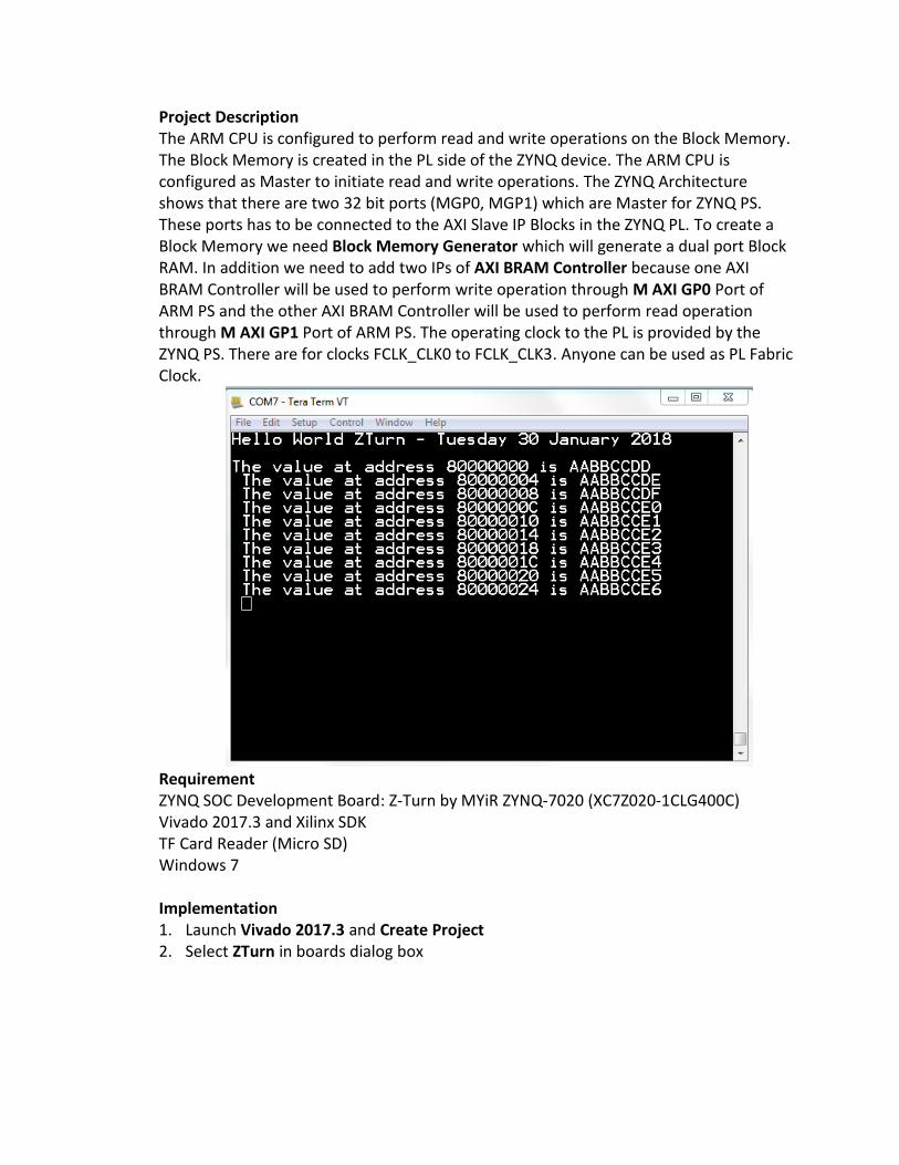
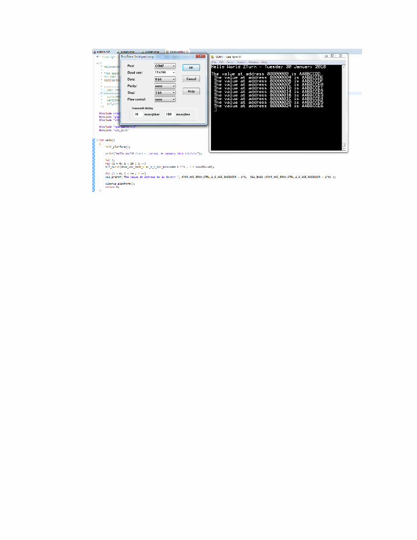
Project Description The ARM CPU is configured to perform read and write operations on the Block Memory. The Block Memory is created in the PL side of the ZYNQ device. The ARM CPU is configured as Master to initiate read and write operations. The ZYNQ Architecture shows that there are two 32 bit ports (MGP0, MGP1) which are Master for ZYNQ PS. These ports has to be connected to the AXI Slave IP Blocks in the ZYNQ PL. To create a Block Memory we need Block Memory Generator which will generate a dual port Block RAM. In addition we need to add two IPs of AXI BRAM Controller because one AXI BRAM Controller will be used to perform write operation through M AXI GP0 Port of ARM PS and the other AXI BRAM Controller will be used to perform read operation through M AXI GP1 Port of ARM PS. The operating clock to the PL is provided by the ZYNQ PS. There are for clocks FCLK_CLK0 to FCLK_CLK3. Anyone can be used as PL Fabric Clock.
Requirement ZYNQ SOC Development Board: Z-Turn by MYiR ZYNQ-7020 (XC7Z020-1CLG400C) Vivado 2017.3 and Xilinx SDK TF Card Reader (Micro SD) Windows 7 Implementation 1. Launch Vivado 2017.3 and Create Project 2. Select ZTurn in boards dialog box
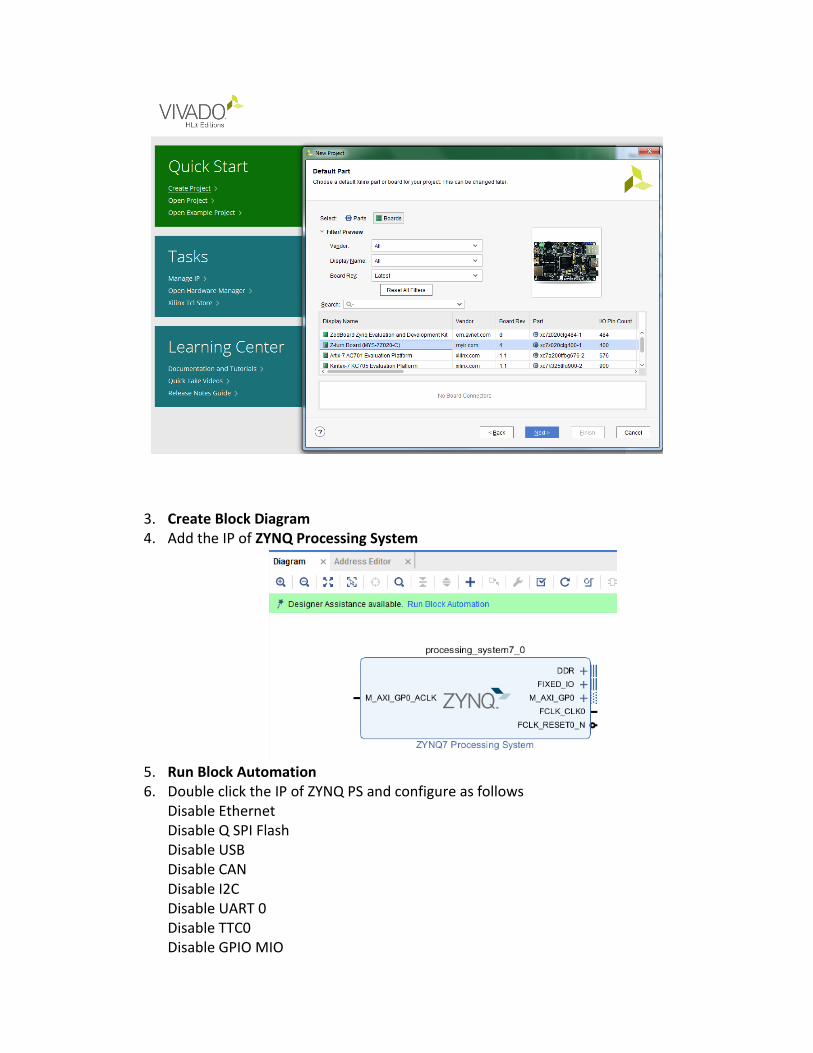
3. Create Block Diagram 4. Add the IP of ZYNQ Processing System
5. Run Block Automation 6. Double click the IP of ZYNQ PS and configure as follows
Disable Ethernet Disable Q SPI Flash Disable USB Disable CAN Disable I2C Disable UART 0 Disable TTC0 Disable GPIO MIO
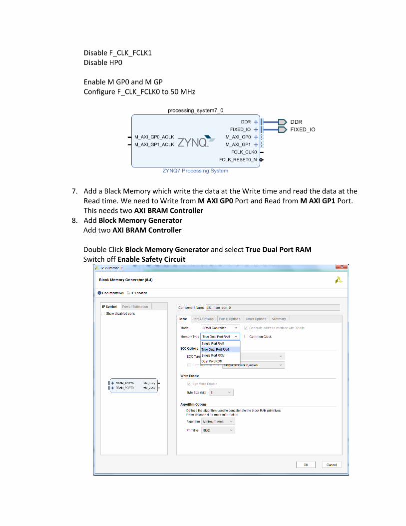
Disable F_CLK_FCLK1 Disable HP0 Enable M GP0 and M GP Configure F_CLK_FCLK0 to 50 MHz
7. Add a Black Memory which write the data at the Write time and read the data at the Read time. We need to Write from M AXI GP0 Port and Read from M AXI GP1 Port. This needs two AXI BRAM Controller
8. Add Block Memory Generator Add two AXI BRAM Controller Double Click Block Memory Generator and select True Dual Port RAM Switch off Enable Safety Circuit
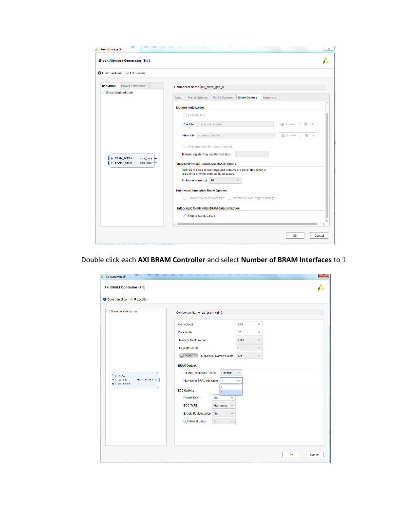
Double click each AXI BRAM Controller and select Number of BRAM Interfaces to 1
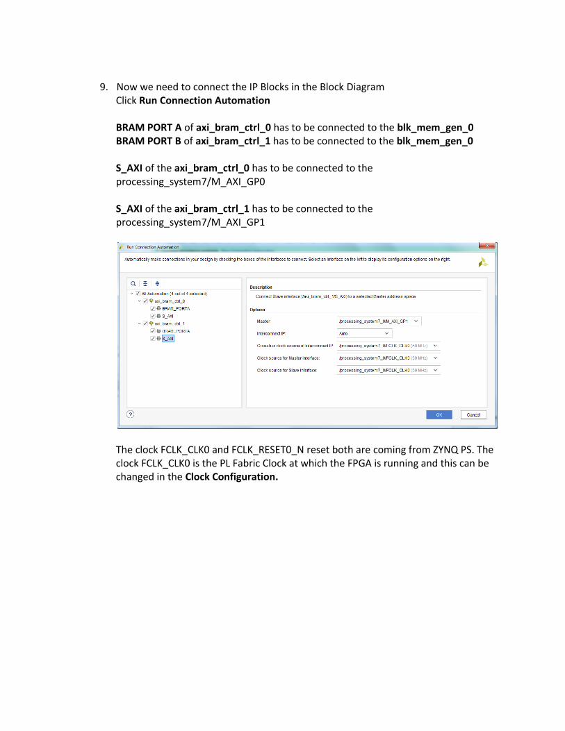
9. Now we need to connect the IP Blocks in the Block Diagram
Click Run Connection Automation BRAM PORT A of axi_bram_ctrl_0 has to be connected to the blk_mem_gen_0 BRAM PORT B of axi_bram_ctrl_1 has to be connected to the blk_mem_gen_0 S_AXI of the axi_bram_ctrl_0 has to be connected to the processing_system7/M_AXI_GP0 S_AXI of the axi_bram_ctrl_1 has to be connected to the processing_system7/M_AXI_GP1
The clock FCLK_CLK0 and FCLK_RESET0_N reset both are coming from ZYNQ PS. The clock FCLK_CLK0 is the PL Fabric Clock at which the FPGA is running and this can be changed in the Clock Configuration.
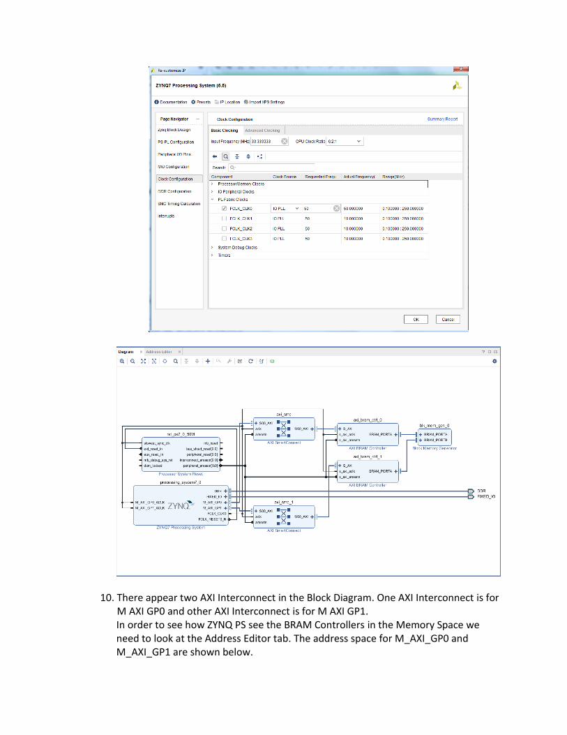
10. There appear two AXI Interconnect in the Block Diagram. One AXI Interconnect is for M AXI GP0 and other AXI Interconnect is for M AXI GP1. In order to see how ZYNQ PS see the BRAM Controllers in the Memory Space we need to look at the Address Editor tab. The address space for M_AXI_GP0 and M_AXI_GP1 are shown below.
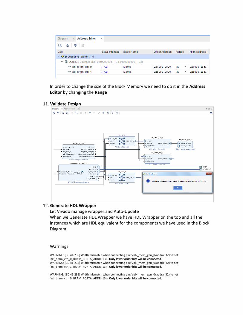
In order to change the size of the Block Memory we need to do it in the Address Editor by changing the Range
11. Validate Design
12. Generate HDL Wrapper
Let Vivado manage wrapper and Auto-Update When we Generate HDL Wrapper we have HDL Wrapper on the top and all the instances which are HDL equivalent for the components we have used in the Block Diagram.
Warnings WARNING: [BD 41-235] Width mismatch when connecting pin: '/blk_mem_gen_0/addra'(32) to net 'axi_bram_ctrl_0_BRAM_PORTA_ADDR'(13) - Only lower order bits will be connected. WARNING: [BD 41-235] Width mismatch when connecting pin: '/blk_mem_gen_0/addrb'(32) to net 'axi_bram_ctrl_1_BRAM_PORTA_ADDR'(13) - Only lower order bits will be connected. WARNING: [BD 41-235] Width mismatch when connecting pin: '/blk_mem_gen_0/addra'(32) to net 'axi_bram_ctrl_0_BRAM_PORTA_ADDR'(13) - Only lower order bits will be connected.
WARNING: [BD 41-235] Width mismatch when connecting pin: '/blk_mem_gen_0/addrb'(32) to net 'axi_bram_ctrl_1_BRAM_PORTA_ADDR'(13) - Only lower order bits will be connected.
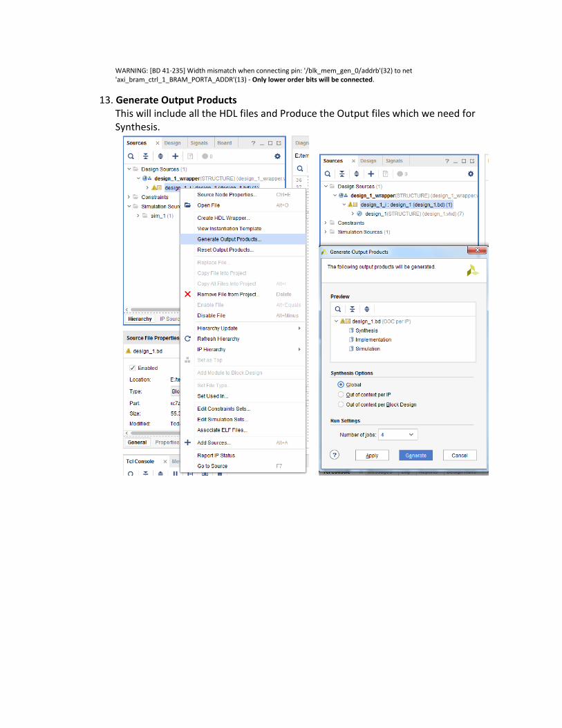
13. Generate Output Products This will include all the HDL files and Produce the Output files which we need for Synthesis.
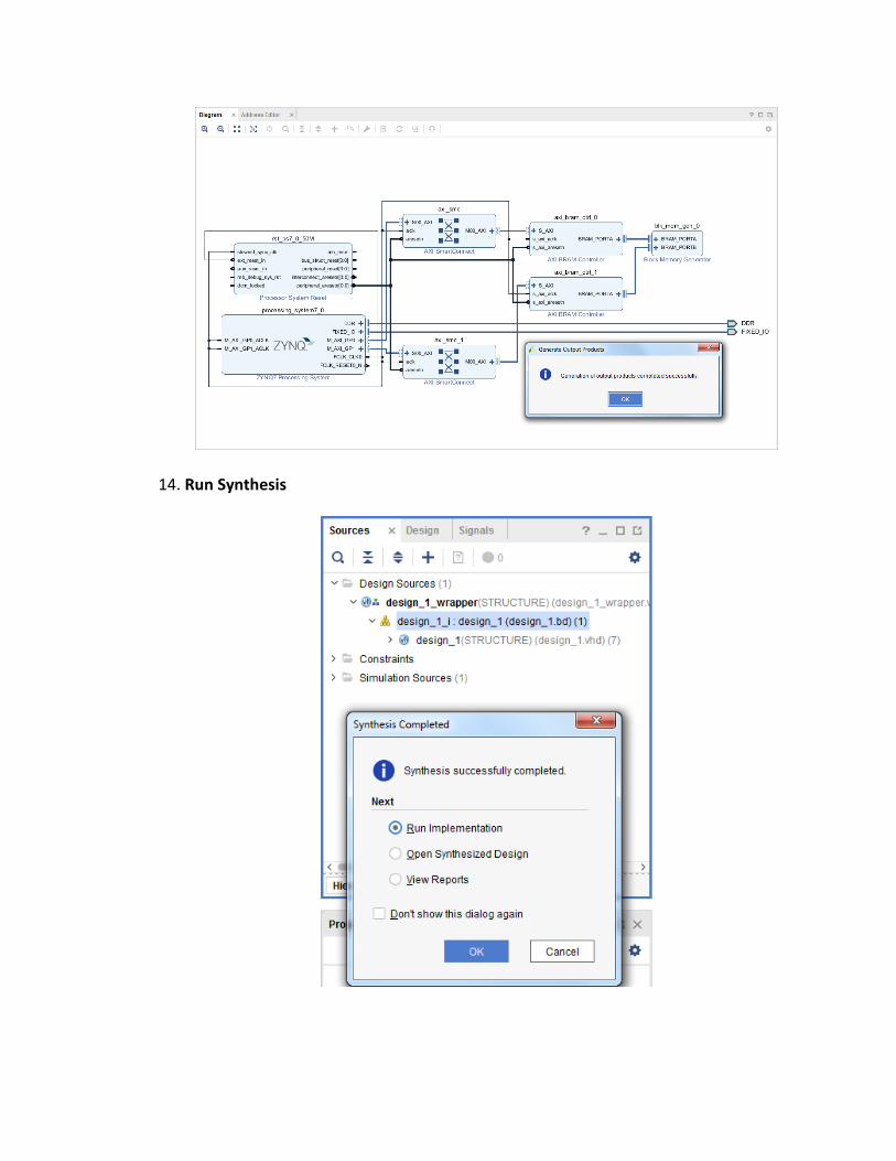
14. Run Synthesis
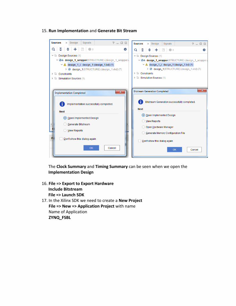
15. Run Implementation and Generate Bit Stream
The Clock Summary and Timing Summary can be seen when we open the Implementation Design
16. File => Export to Export Hardware Include Bitstream File => Launch SDK
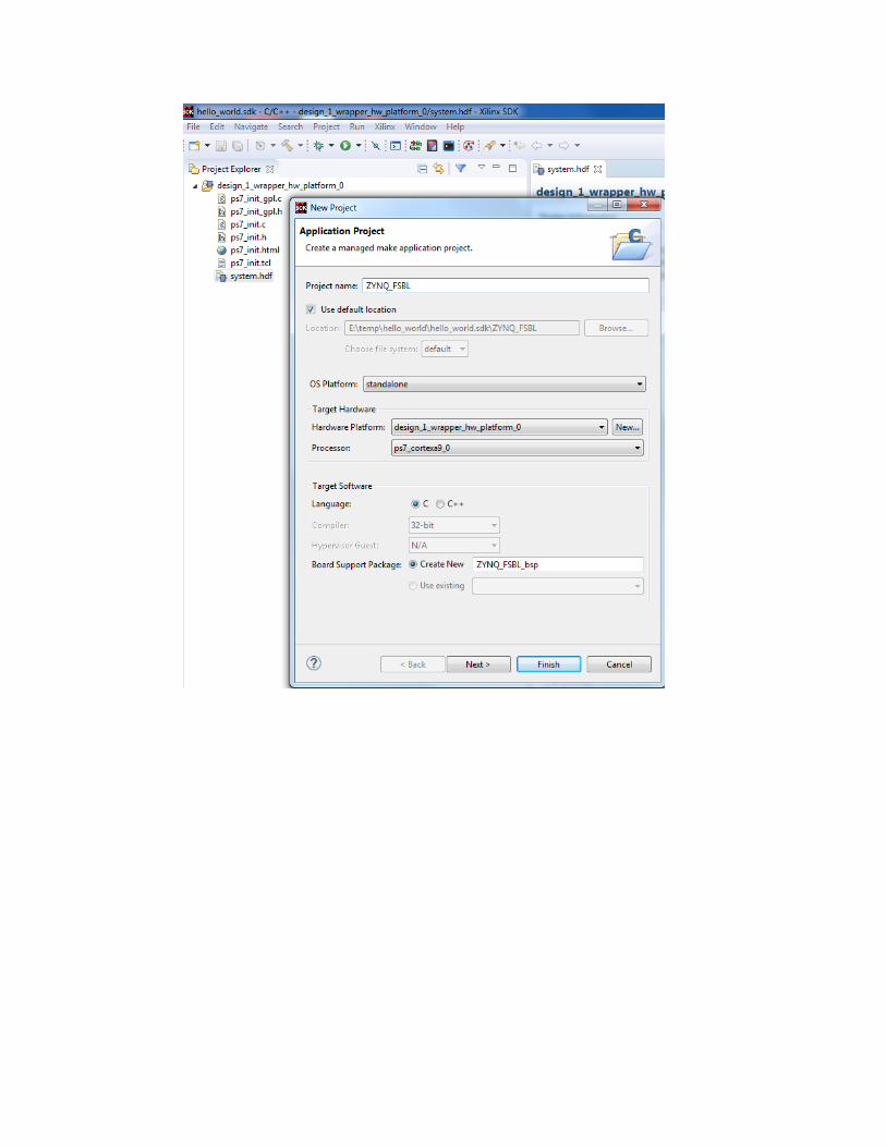
17. In the Xilinx SDK we need to create a New Project File => New => Application Project with name Name of Application ZYNQ_FSBL
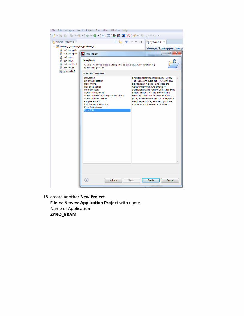
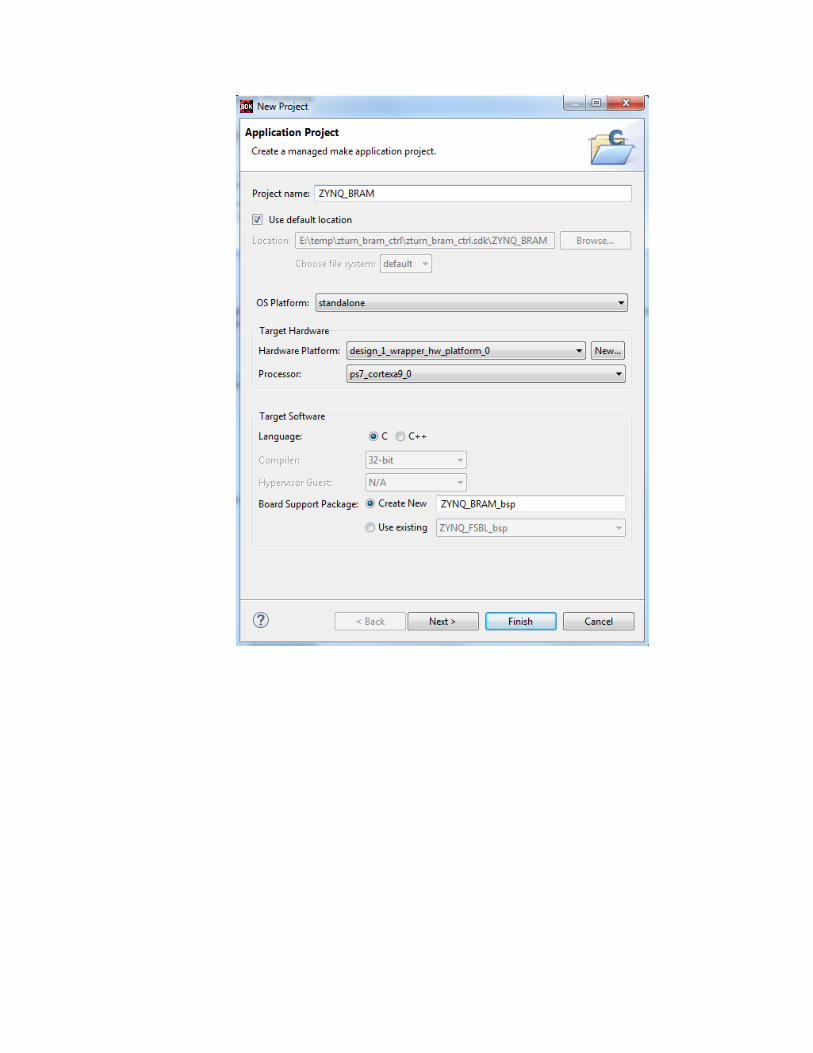
18. create another New Project File => New => Application Project with name Name of Application ZYNQ_BRAM
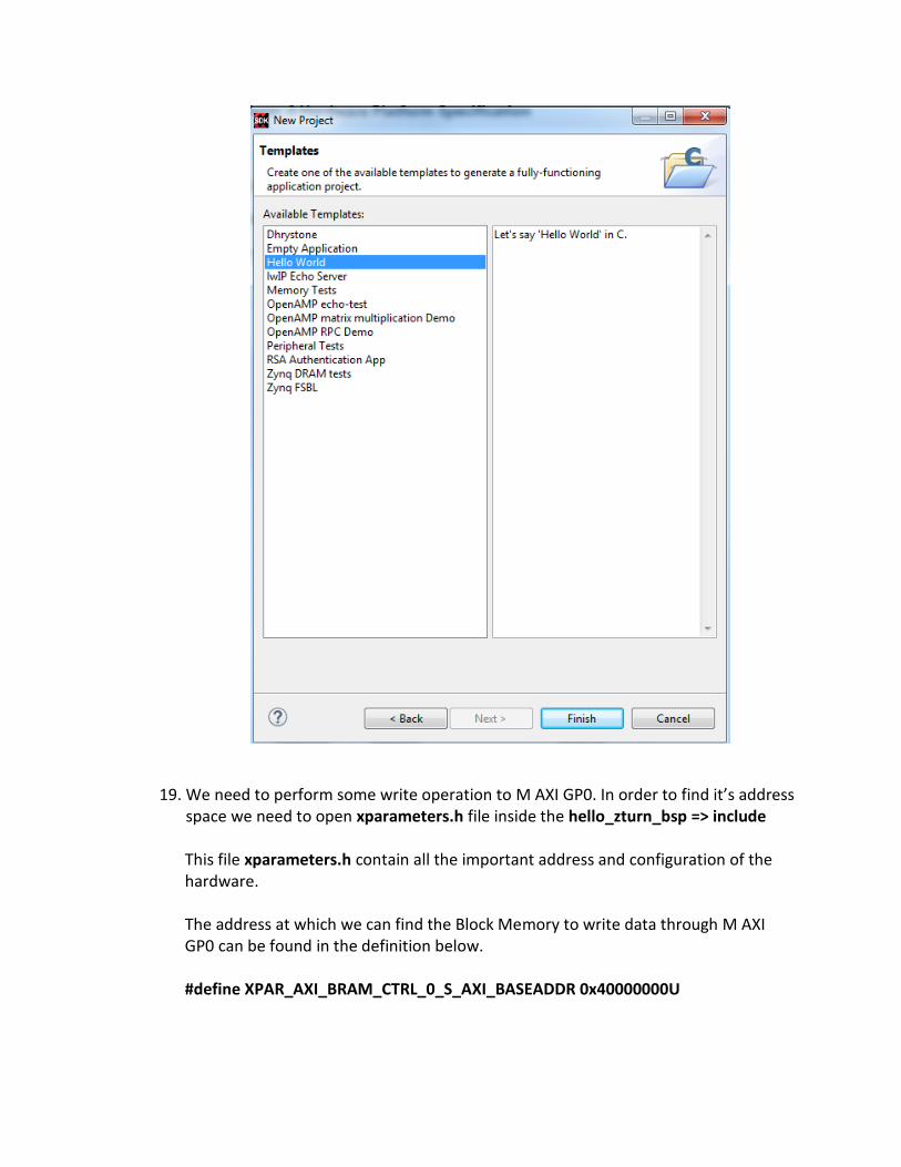
19. We need to perform some write operation to M AXI GP0. In order to find it’s address space we need to open xparameters.h file inside the hello_zturn_bsp => include This file xparameters.h contain all the important address and configuration of the hardware. The address at which we can find the Block Memory to write data through M AXI GP0 can be found in the definition below. #define XPAR_AXI_BRAM_CTRL_0_S_AXI_BASEADDR 0x40000000U
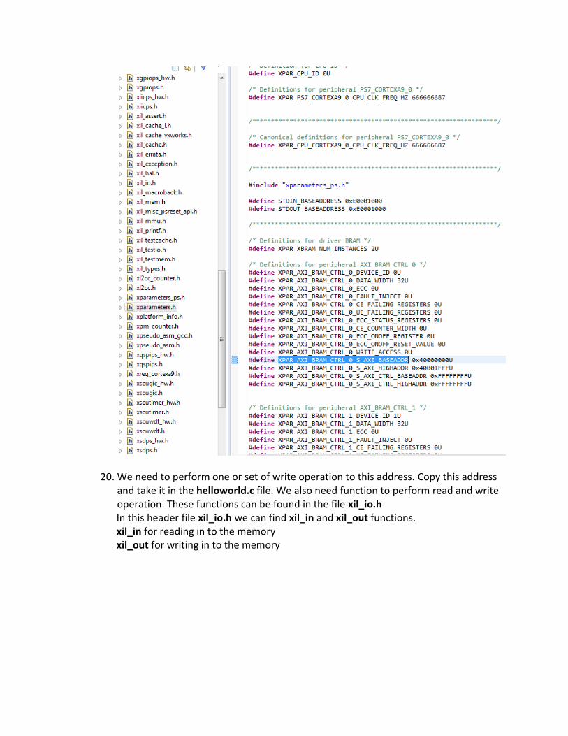
20. We need to perform one or set of write operation to this address. Copy this address and take it in the helloworld.c file. We also need function to perform read and write operation. These functions can be found in the file xil_io.h In this header file xil_io.h we can find xil_in and xil_out functions. xil_in for reading in to the memory xil_out for writing in to the memory
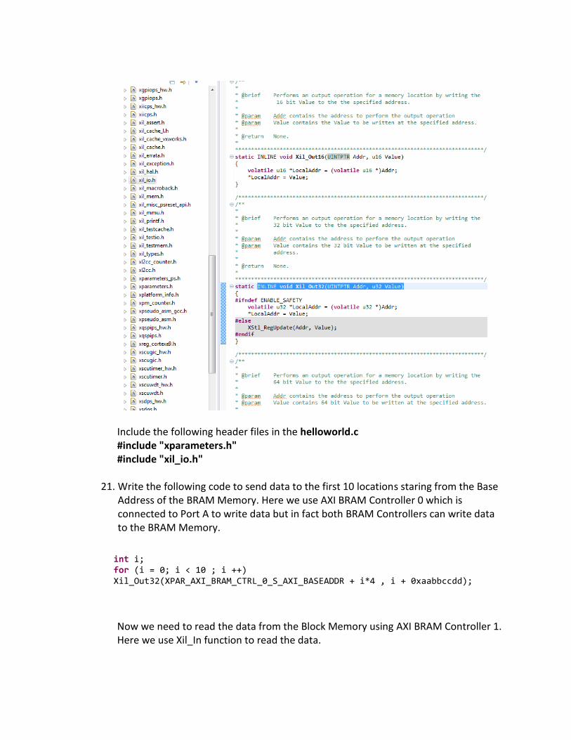
Include the following header files in the helloworld.c #include "xparameters.h" #include "xil_io.h"
21. Write the following code to send data to the first 10 locations staring from the Base Address of the BRAM Memory. Here we use AXI BRAM Controller 0 which is connected to Port A to write data but in fact both BRAM Controllers can write data to the BRAM Memory.
int i; for (i = 0; i < 10 ; i ++) Xil_Out32(XPAR_AXI_BRAM_CTRL_0_S_AXI_BASEADDR + i*4 , i + 0xaabbccdd);
Now we need to read the data from the Block Memory using AXI BRAM Controller 1. Here we use Xil_In function to read the data.
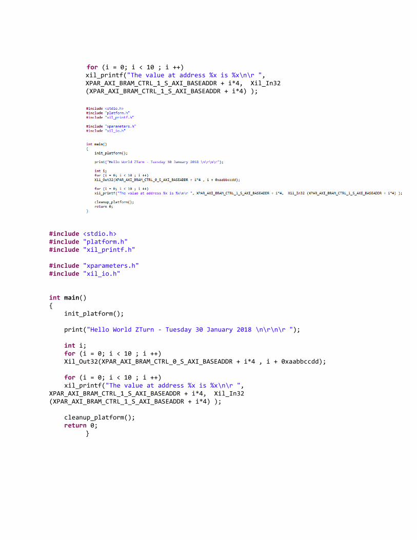
for (i = 0; i < 10 ; i ++) xil_printf("The value at address %x is %x\n\r ", XPAR_AXI_BRAM_CTRL_1_S_AXI_BASEADDR + i*4, Xil_In32 (XPAR_AXI_BRAM_CTRL_1_S_AXI_BASEADDR + i*4) );
#include <stdio.h> #include "platform.h" #include "xil_printf.h" #include "xparameters.h" #include "xil_io.h" int main() { init_platform(); print("Hello World ZTurn - Tuesday 30 January 2018 \n\r\n\r "); int i; for (i = 0; i < 10 ; i ++) Xil_Out32(XPAR_AXI_BRAM_CTRL_0_S_AXI_BASEADDR + i*4 , i + 0xaabbccdd); for (i = 0; i < 10 ; i ++) xil_printf("The value at address %x is %x\n\r ", XPAR_AXI_BRAM_CTRL_1_S_AXI_BASEADDR + i*4, Xil_In32 (XPAR_AXI_BRAM_CTRL_1_S_AXI_BASEADDR + i*4) ); cleanup_platform(); return 0;
}
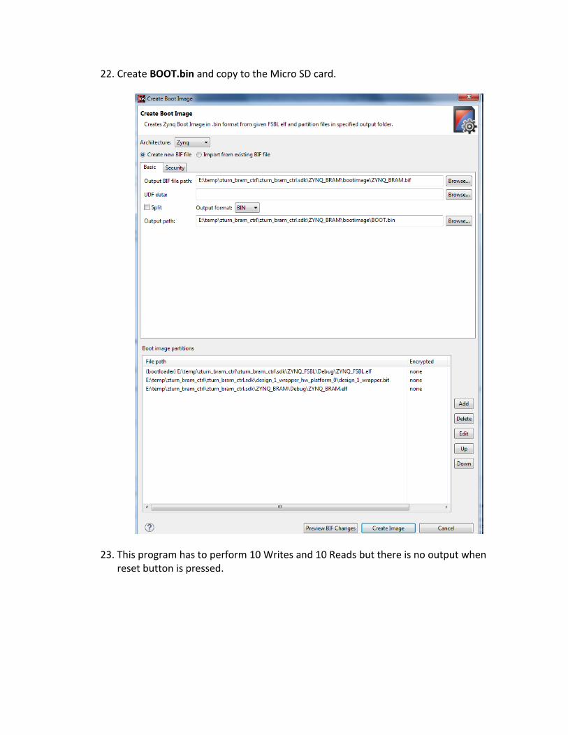
22. Create BOOT.bin and copy to the Micro SD card.
23. This program has to perform 10 Writes and 10 Reads but there is no output when reset button is pressed.