Embed Size (px)
Citation preview
Using ModelSim to Simulate LogicCircuits in Verilog Designs
For Quartus II 15.0
1 Introduction
This tutorial is a basic introduction to ModelSim, a Mentor Graphics simulation tool for logic circuits. We showhow to perform functional and timing simulations of logic circuits implemented by using Quartus II CAD software.
The reader is expected to have the basic knowledge of the Verilog hardware description language, and the AlteraQuartus® II CAD software.
Contents:
• Introduction to simulation
• What is ModelSim?
• Functional simulation using ModelSim
• Timing simulation using ModelSim
Altera Corporation - University ProgramMay 2015
1
USING MODELSIM TO SIMULATE LOGIC CIRCUITS IN VERILOG DESIGNS For Quartus II 15.0
2 Background
Designers of digital systems are inevitably faced with the task of testing their designs. Each design can be composedof many modules, each of which has to be tested in isolation and then integrated into a design when it operatescorrectly.
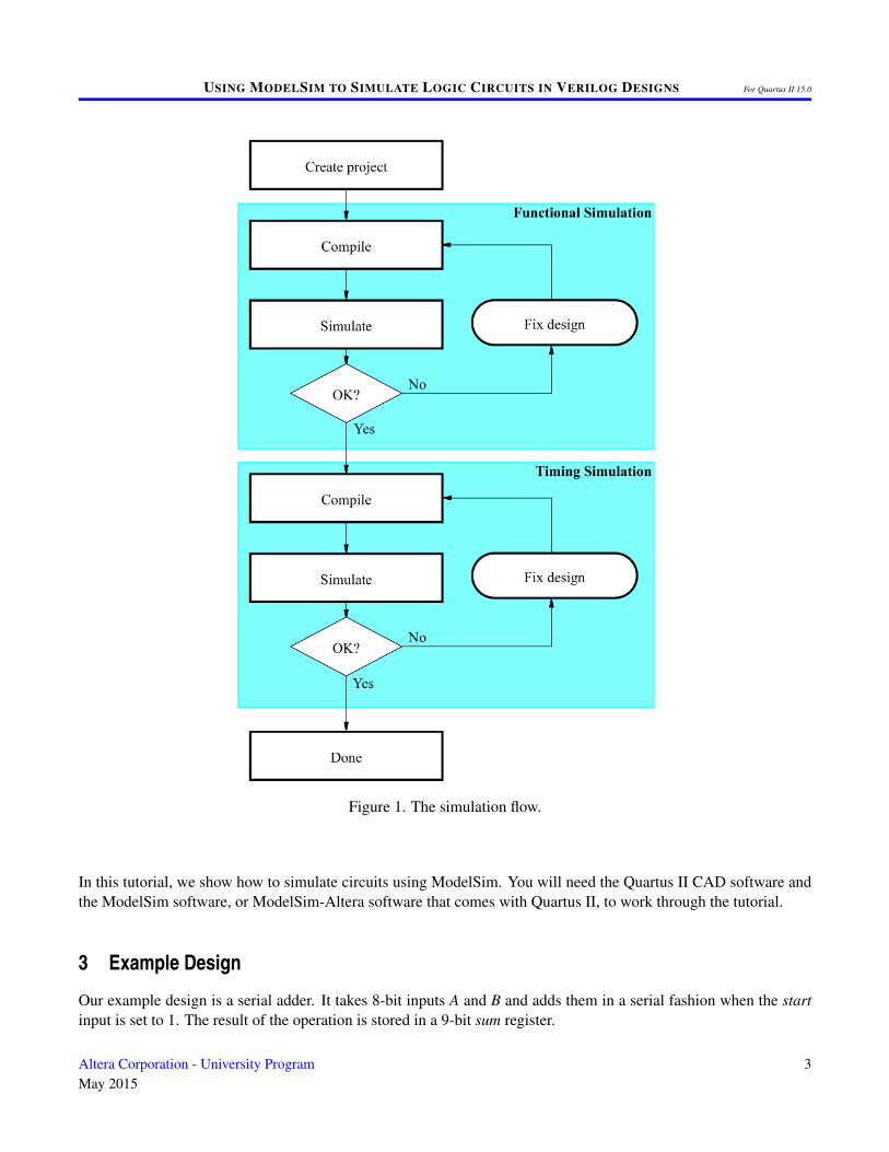
To verify that a design operates correctly we use simulation, which is a process of testing the design by applyinginputs to a circuit and observing its behavior. The output of a simulation is a set of waveforms that show how acircuit behaves based on a given sequence of inputs. The general flow of a simulation is shown in Figure 1.
There are two main types of simulation: functional and timing simulation. The functional simulation tests the logicaloperation of a circuit without accounting for delays in the circuit. Signals are propagated through the circuit usinglogic and wiring delays of zero. This simulation is fast and useful for checking the fundamental correctness of thedesigned circuit.
The second step of the simulation process is the timing simulation. It is a more complex type of simulation, wherelogic components and wires take some time to respond to input stimuli. In addition to testing the logical operation ofthe circuit, it shows the timing of signals in the circuit. This type of simulation is more realistic than the functionalsimulation; however, it takes longer to perform.
2 Altera Corporation - University ProgramMay 2015
USING MODELSIM TO SIMULATE LOGIC CIRCUITS IN VERILOG DESIGNS For Quartus II 15.0
Figure 1. The simulation flow.
In this tutorial, we show how to simulate circuits using ModelSim. You will need the Quartus II CAD software andthe ModelSim software, or ModelSim-Altera software that comes with Quartus II, to work through the tutorial.
3 Example Design
Our example design is a serial adder. It takes 8-bit inputs A and B and adds them in a serial fashion when the startinput is set to 1. The result of the operation is stored in a 9-bit sum register.
Altera Corporation - University ProgramMay 2015
3
USING MODELSIM TO SIMULATE LOGIC CIRCUITS IN VERILOG DESIGNS For Quartus II 15.0
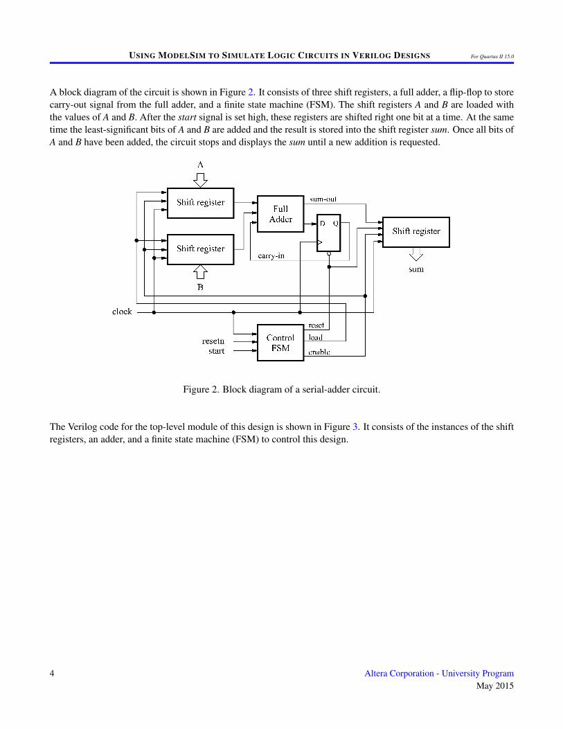
A block diagram of the circuit is shown in Figure 2. It consists of three shift registers, a full adder, a flip-flop to storecarry-out signal from the full adder, and a finite state machine (FSM). The shift registers A and B are loaded withthe values of A and B. After the start signal is set high, these registers are shifted right one bit at a time. At the sametime the least-significant bits of A and B are added and the result is stored into the shift register sum. Once all bits ofA and B have been added, the circuit stops and displays the sum until a new addition is requested.
Figure 2. Block diagram of a serial-adder circuit.
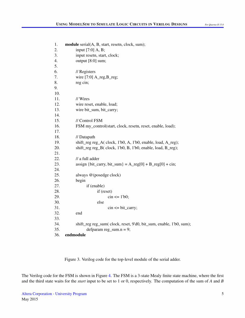
The Verilog code for the top-level module of this design is shown in Figure 3. It consists of the instances of the shiftregisters, an adder, and a finite state machine (FSM) to control this design.
4 Altera Corporation - University ProgramMay 2015
USING MODELSIM TO SIMULATE LOGIC CIRCUITS IN VERILOG DESIGNS For Quartus II 15.0
1. module serial(A, B, start, resetn, clock, sum);2. input [7:0] A, B;3. input resetn, start, clock;4. output [8:0] sum;5.6. // Registers7. wire [7:0] A_reg,B_reg;8. reg cin;9.10.11. // Wires12. wire reset, enable, load;13. wire bit_sum, bit_carry;14.15. // Control FSM16. FSM my_control(start, clock, resetn, reset, enable, load);17.18. // Datapath19. shift_reg reg_A( clock, 1'b0, A, 1'b0, enable, load, A_reg);20. shift_reg reg_B( clock, 1'b0, B, 1'b0, enable, load, B_reg);21.22. // a full adder23. assign {bit_carry, bit_sum} = A_reg[0] + B_reg[0] + cin;24.25. always @(posedge clock)26. begin27. if (enable)28. if (reset)29. cin <= 1'b0;30. else31. cin <= bit_carry;32. end33.34. shift_reg reg_sum( clock, reset, 9'd0, bit_sum, enable, 1'b0, sum);35. defparam reg_sum.n = 9;36. endmodule
Figure 3. Verilog code for the top-level module of the serial adder.
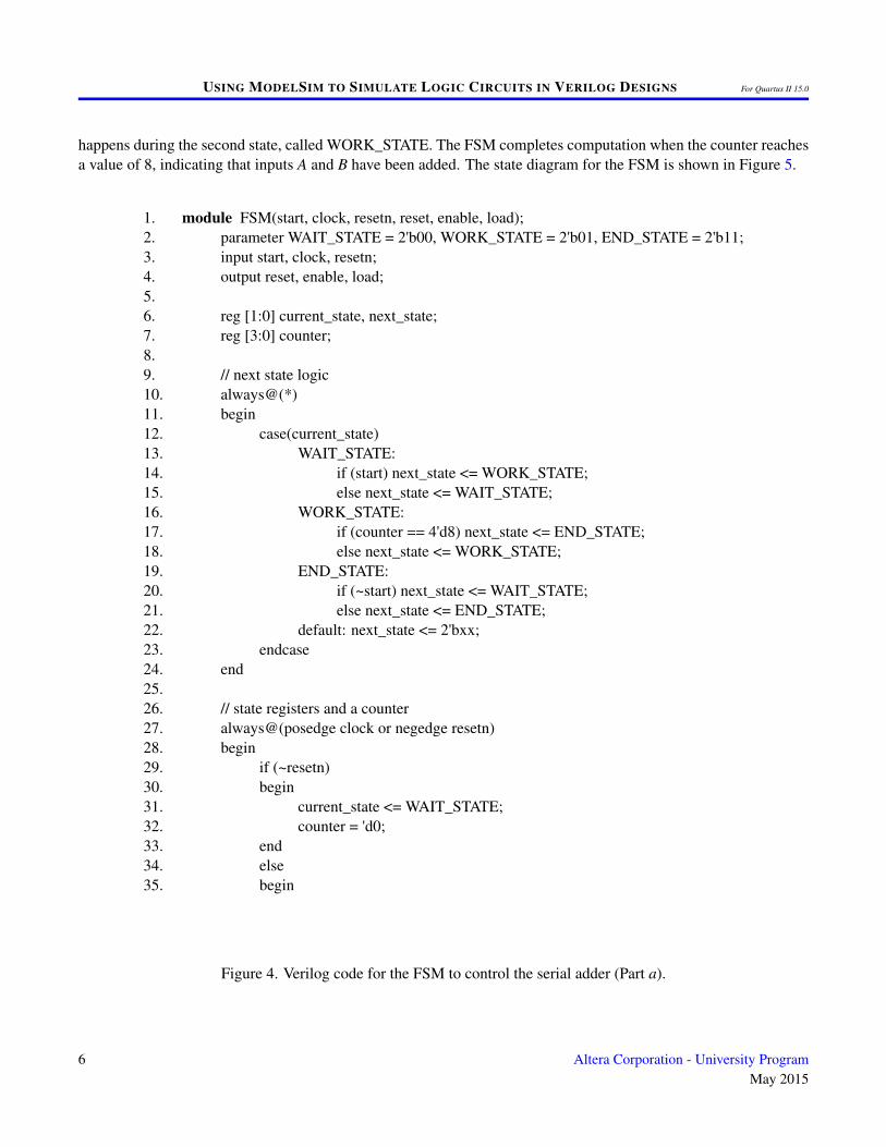
The Verilog code for the FSM is shown in Figure 4. The FSM is a 3-state Mealy finite state machine, where the firstand the third state waits for the start input to be set to 1 or 0, respectively. The computation of the sum of A and B
Altera Corporation - University ProgramMay 2015
5
USING MODELSIM TO SIMULATE LOGIC CIRCUITS IN VERILOG DESIGNS For Quartus II 15.0
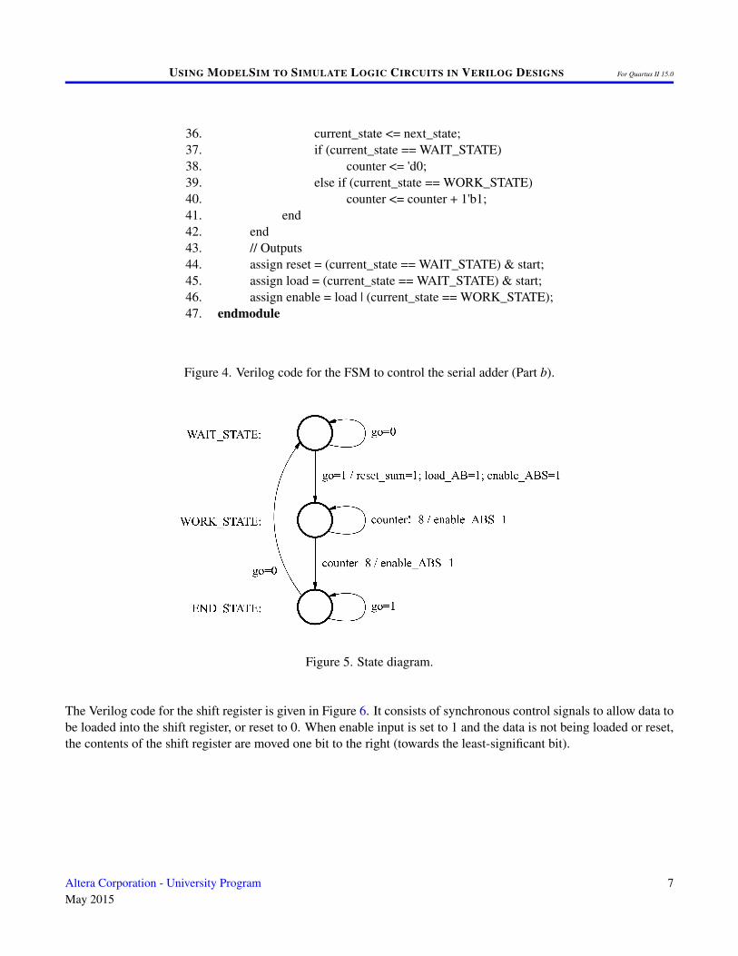
happens during the second state, called WORK_STATE. The FSM completes computation when the counter reachesa value of 8, indicating that inputs A and B have been added. The state diagram for the FSM is shown in Figure 5.
1. module FSM(start, clock, resetn, reset, enable, load);2. parameter WAIT_STATE = 2'b00, WORK_STATE = 2'b01, END_STATE = 2'b11;3. input start, clock, resetn;4. output reset, enable, load;5.6. reg [1:0] current_state, next_state;7. reg [3:0] counter;8.9. // next state logic10. always@(*)11. begin12. case(current_state)13. WAIT_STATE:14. if (start) next_state <= WORK_STATE;15. else next_state <= WAIT_STATE;16. WORK_STATE:17. if (counter == 4'd8) next_state <= END_STATE;18. else next_state <= WORK_STATE;19. END_STATE:20. if (~start) next_state <= WAIT_STATE;21. else next_state <= END_STATE;22. default: next_state <= 2'bxx;23. endcase24. end25.26. // state registers and a counter27. always@(posedge clock or negedge resetn)28. begin29. if (~resetn)30. begin31. current_state <= WAIT_STATE;32. counter = 'd0;33. end34. else35. begin
Figure 4. Verilog code for the FSM to control the serial adder (Part a).
6 Altera Corporation - University ProgramMay 2015
USING MODELSIM TO SIMULATE LOGIC CIRCUITS IN VERILOG DESIGNS For Quartus II 15.0
36. current_state <= next_state;37. if (current_state == WAIT_STATE)38. counter <= 'd0;39. else if (current_state == WORK_STATE)40. counter <= counter + 1'b1;41. end42. end43. // Outputs44. assign reset = (current_state == WAIT_STATE) & start;45. assign load = (current_state == WAIT_STATE) & start;46. assign enable = load | (current_state == WORK_STATE);47. endmodule
Figure 4. Verilog code for the FSM to control the serial adder (Part b).
Figure 5. State diagram.
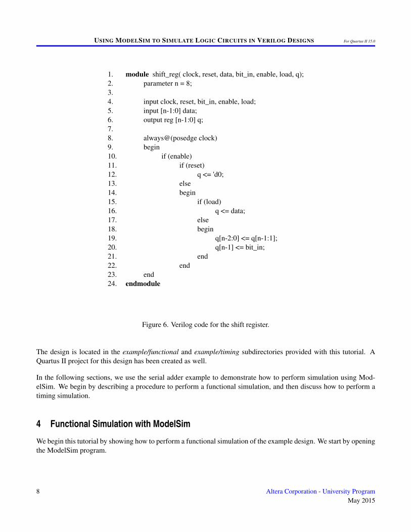
The Verilog code for the shift register is given in Figure 6. It consists of synchronous control signals to allow data tobe loaded into the shift register, or reset to 0. When enable input is set to 1 and the data is not being loaded or reset,the contents of the shift register are moved one bit to the right (towards the least-significant bit).
Altera Corporation - University ProgramMay 2015
7
USING MODELSIM TO SIMULATE LOGIC CIRCUITS IN VERILOG DESIGNS For Quartus II 15.0
1. module shift_reg( clock, reset, data, bit_in, enable, load, q);2. parameter n = 8;3.4. input clock, reset, bit_in, enable, load;5. input [n-1:0] data;6. output reg [n-1:0] q;7.8. always@(posedge clock)9. begin10. if (enable)11. if (reset)12. q <= 'd0;13. else14. begin15. if (load)16. q <= data;17. else18. begin19. q[n-2:0] <= q[n-1:1];20. q[n-1] <= bit_in;21. end22. end23. end24. endmodule
Figure 6. Verilog code for the shift register.
The design is located in the example/functional and example/timing subdirectories provided with this tutorial. AQuartus II project for this design has been created as well.
In the following sections, we use the serial adder example to demonstrate how to perform simulation using Mod-elSim. We begin by describing a procedure to perform a functional simulation, and then discuss how to perform atiming simulation.
4 Functional Simulation with ModelSim
We begin this tutorial by showing how to perform a functional simulation of the example design. We start by openingthe ModelSim program.
8 Altera Corporation - University ProgramMay 2015
USING MODELSIM TO SIMULATE LOGIC CIRCUITS IN VERILOG DESIGNS For Quartus II 15.0
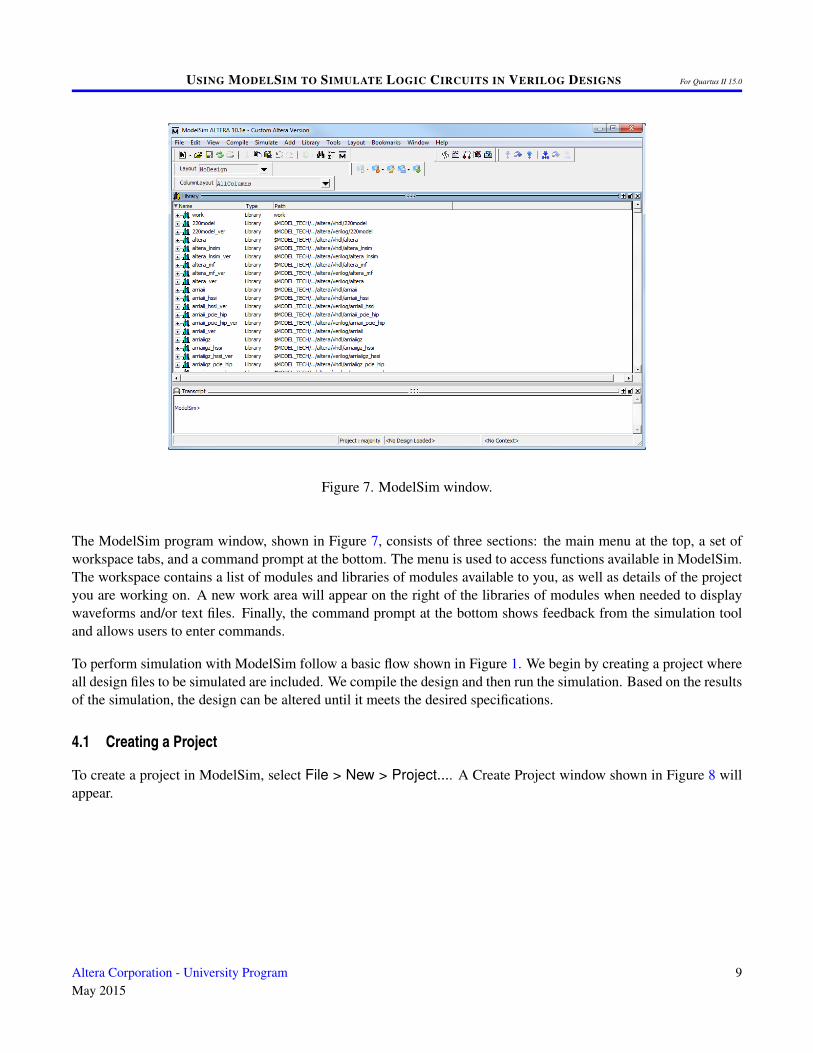
Figure 7. ModelSim window.
The ModelSim program window, shown in Figure 7, consists of three sections: the main menu at the top, a set ofworkspace tabs, and a command prompt at the bottom. The menu is used to access functions available in ModelSim.The workspace contains a list of modules and libraries of modules available to you, as well as details of the projectyou are working on. A new work area will appear on the right of the libraries of modules when needed to displaywaveforms and/or text files. Finally, the command prompt at the bottom shows feedback from the simulation tooland allows users to enter commands.
To perform simulation with ModelSim follow a basic flow shown in Figure 1. We begin by creating a project whereall design files to be simulated are included. We compile the design and then run the simulation. Based on the resultsof the simulation, the design can be altered until it meets the desired specifications.
4.1 Creating a Project
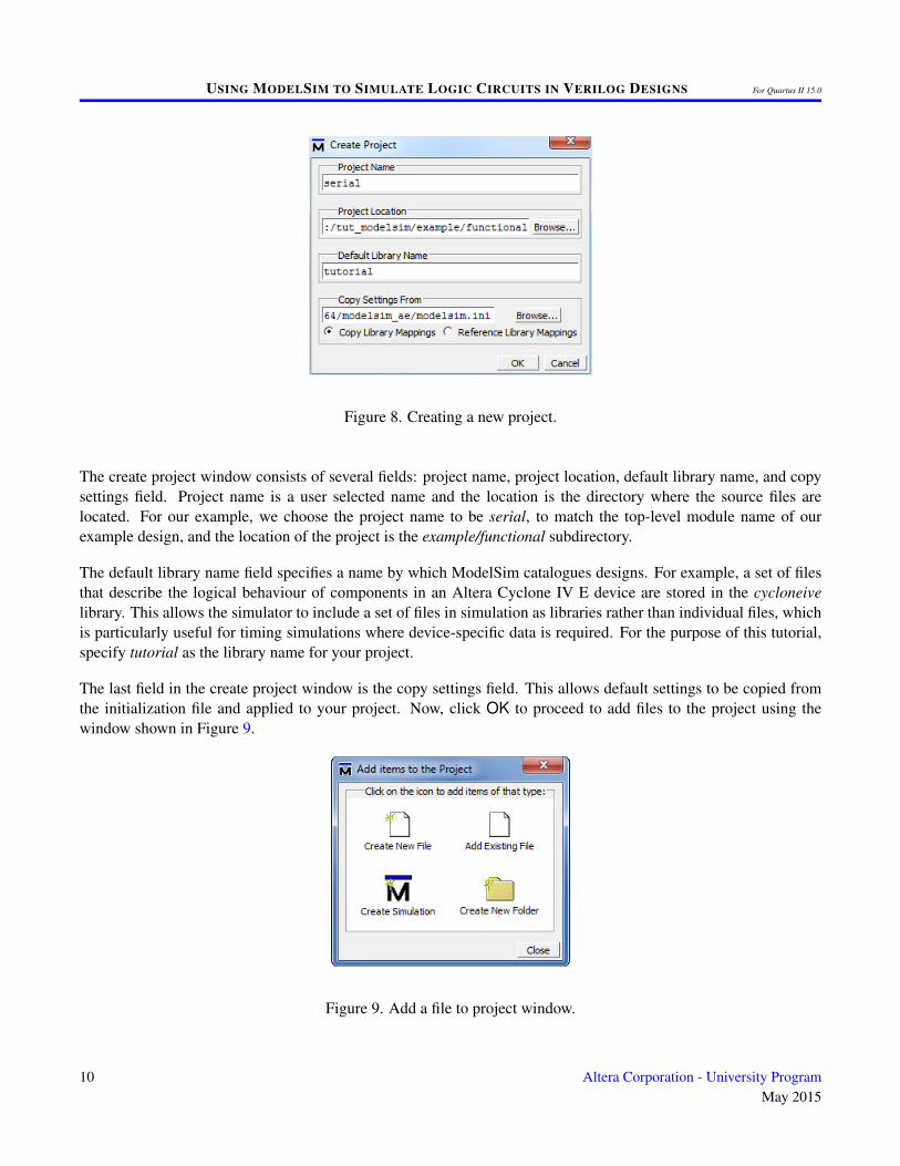
To create a project in ModelSim, select File > New > Project.... A Create Project window shown in Figure 8 willappear.
Altera Corporation - University ProgramMay 2015
9
USING MODELSIM TO SIMULATE LOGIC CIRCUITS IN VERILOG DESIGNS For Quartus II 15.0
Figure 8. Creating a new project.
The create project window consists of several fields: project name, project location, default library name, and copysettings field. Project name is a user selected name and the location is the directory where the source files arelocated. For our example, we choose the project name to be serial, to match the top-level module name of ourexample design, and the location of the project is the example/functional subdirectory.
The default library name field specifies a name by which ModelSim catalogues designs. For example, a set of filesthat describe the logical behaviour of components in an Altera Cyclone IV E device are stored in the cycloneivelibrary. This allows the simulator to include a set of files in simulation as libraries rather than individual files, whichis particularly useful for timing simulations where device-specific data is required. For the purpose of this tutorial,specify tutorial as the library name for your project.
The last field in the create project window is the copy settings field. This allows default settings to be copied fromthe initialization file and applied to your project. Now, click OK to proceed to add files to the project using thewindow shown in Figure 9.
Figure 9. Add a file to project window.
10 Altera Corporation - University ProgramMay 2015
USING MODELSIM TO SIMULATE LOGIC CIRCUITS IN VERILOG DESIGNS For Quartus II 15.0
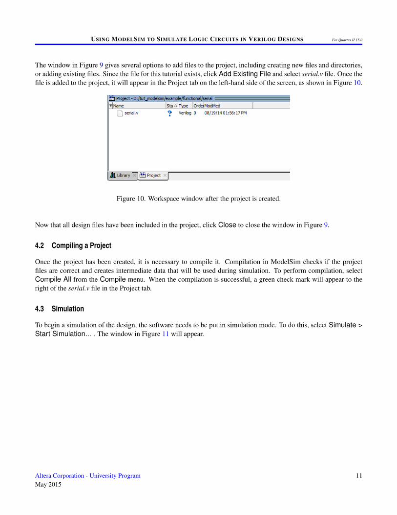
The window in Figure 9 gives several options to add files to the project, including creating new files and directories,or adding existing files. Since the file for this tutorial exists, click Add Existing File and select serial.v file. Once thefile is added to the project, it will appear in the Project tab on the left-hand side of the screen, as shown in Figure 10.
Figure 10. Workspace window after the project is created.
Now that all design files have been included in the project, click Close to close the window in Figure 9.
4.2 Compiling a Project
Once the project has been created, it is necessary to compile it. Compilation in ModelSim checks if the projectfiles are correct and creates intermediate data that will be used during simulation. To perform compilation, selectCompile All from the Compile menu. When the compilation is successful, a green check mark will appear to theright of the serial.v file in the Project tab.
4.3 Simulation
To begin a simulation of the design, the software needs to be put in simulation mode. To do this, select Simulate >Start Simulation... . The window in Figure 11 will appear.
Altera Corporation - University ProgramMay 2015
11
USING MODELSIM TO SIMULATE LOGIC CIRCUITS IN VERILOG DESIGNS For Quartus II 15.0
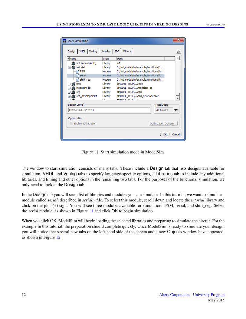
Figure 11. Start simulation mode in ModelSim.
The window to start simulation consists of many tabs. These include a Design tab that lists designs available forsimulation, VHDL and Verilog tabs to specify language-specific options, a Libraries tab to include any additionallibraries, and timing and other options in the remaining two tabs. For the purposes of the functional simulation, weonly need to look at the Design tab.
In the Design tab you will see a list of libraries and modules you can simulate. In this tutorial, we want to simulate amodule called serial, described in serial.v file. To select this module, scroll down and locate the tutorial library andclick on the plus (+) sign. You will see three modules available for simulation: FSM, serial, and shift_reg. Selectthe serial module, as shown in Figure 11 and click OK to begin simulation.
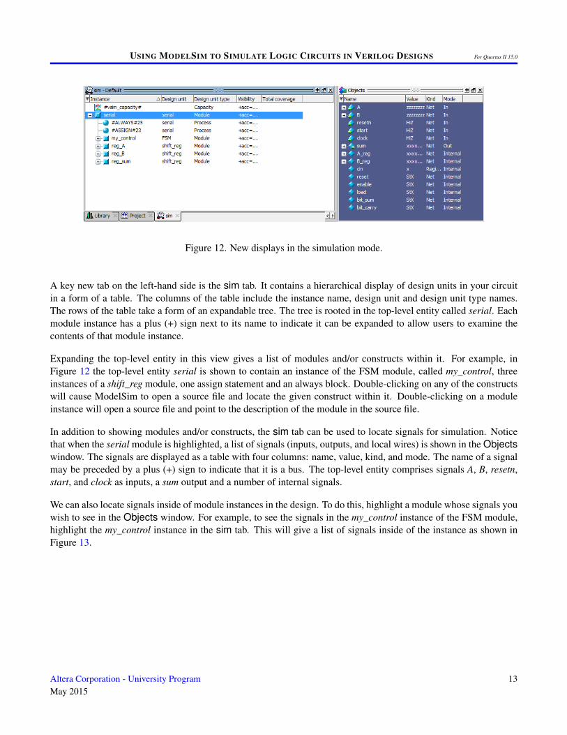
When you click OK, ModelSim will begin loading the selected libraries and preparing to simulate the circuit. For theexample in this tutorial, the preparation should complete quickly. Once ModelSim is ready to simulate your design,you will notice that several new tabs on the left-hand side of the screen and a new Objects window have appeared,as shown in Figure 12.
12 Altera Corporation - University ProgramMay 2015
USING MODELSIM TO SIMULATE LOGIC CIRCUITS IN VERILOG DESIGNS For Quartus II 15.0
Figure 12. New displays in the simulation mode.
A key new tab on the left-hand side is the sim tab. It contains a hierarchical display of design units in your circuitin a form of a table. The columns of the table include the instance name, design unit and design unit type names.The rows of the table take a form of an expandable tree. The tree is rooted in the top-level entity called serial. Eachmodule instance has a plus (+) sign next to its name to indicate it can be expanded to allow users to examine thecontents of that module instance.
Expanding the top-level entity in this view gives a list of modules and/or constructs within it. For example, inFigure 12 the top-level entity serial is shown to contain an instance of the FSM module, called my_control, threeinstances of a shift_reg module, one assign statement and an always block. Double-clicking on any of the constructswill cause ModelSim to open a source file and locate the given construct within it. Double-clicking on a moduleinstance will open a source file and point to the description of the module in the source file.
In addition to showing modules and/or constructs, the sim tab can be used to locate signals for simulation. Noticethat when the serial module is highlighted, a list of signals (inputs, outputs, and local wires) is shown in the Objectswindow. The signals are displayed as a table with four columns: name, value, kind, and mode. The name of a signalmay be preceded by a plus (+) sign to indicate that it is a bus. The top-level entity comprises signals A, B, resetn,start, and clock as inputs, a sum output and a number of internal signals.
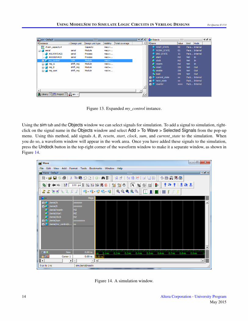
We can also locate signals inside of module instances in the design. To do this, highlight a module whose signals youwish to see in the Objects window. For example, to see the signals in the my_control instance of the FSM module,highlight the my_control instance in the sim tab. This will give a list of signals inside of the instance as shown inFigure 13.
Altera Corporation - University ProgramMay 2015
13
USING MODELSIM TO SIMULATE LOGIC CIRCUITS IN VERILOG DESIGNS For Quartus II 15.0
Figure 13. Expanded my_control instance.
Using the sim tab and the Objects window we can select signals for simulation. To add a signal to simulation, right-click on the signal name in the Objects window and select Add > To Wave > Selected Signals from the pop-upmenu. Using this method, add signals A, B, resetn, start, clock, sum, and current_state to the simulation. Whenyou do so, a waveform window will appear in the work area. Once you have added these signals to the simulation,press the Undock button in the top-right corner of the waveform window to make it a separate window, as shown inFigure 14.
Figure 14. A simulation window.
14 Altera Corporation - University ProgramMay 2015
USING MODELSIM TO SIMULATE LOGIC CIRCUITS IN VERILOG DESIGNS For Quartus II 15.0
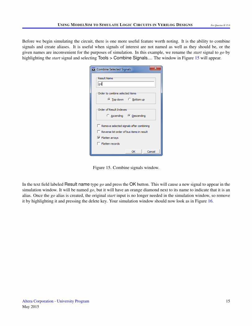
Before we begin simulating the circuit, there is one more useful feature worth noting. It is the ability to combinesignals and create aliases. It is useful when signals of interest are not named as well as they should be, or thegiven names are inconvenient for the purposes of simulation. In this example, we rename the start signal to go byhighlighting the start signal and selecting Tools > Combine Signals.... The window in Figure 15 will appear.
Figure 15. Combine signals window.
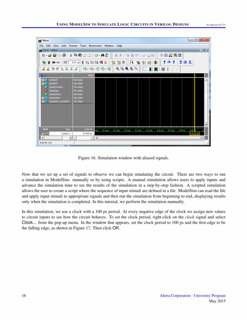
In the text field labeled Result name type go and press the OK button. This will cause a new signal to appear in thesimulation window. It will be named go, but it will have an orange diamond next to its name to indicate that it is analias. Once the go alias is created, the original start input is no longer needed in the simulation window, so removeit by highlighting it and pressing the delete key. Your simulation window should now look as in Figure 16.
Altera Corporation - University ProgramMay 2015
15
USING MODELSIM TO SIMULATE LOGIC CIRCUITS IN VERILOG DESIGNS For Quartus II 15.0
Figure 16. Simulation window with aliased signals.
Now that we set up a set of signals to observe we can begin simulating the circuit. There are two ways to runa simulation in ModelSim: manually or by using scripts. A manual simulation allows users to apply inputs andadvance the simulation time to see the results of the simulation in a step-by-step fashion. A scripted simulationallows the user to create a script where the sequence of input stimuli are defined in a file. ModelSim can read the fileand apply input stimuli to appropriate signals and then run the simulation from beginning to end, displaying resultsonly when the simulation is completed. In this tutorial, we perform the simulation manually.
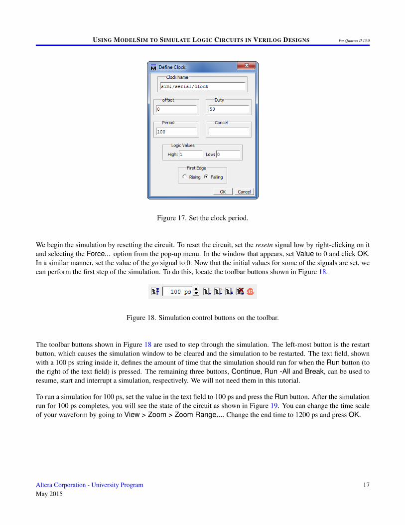
In this simulation, we use a clock with a 100 ps period. At every negative edge of the clock we assign new valuesto circuit inputs to see how the circuit behaves. To set the clock period, right-click on the clock signal and selectClock... from the pop-up menu. In the window that appears, set the clock period to 100 ps and the first edge to bethe falling edge, as shown in Figure 17. Then click OK.
16 Altera Corporation - University ProgramMay 2015
USING MODELSIM TO SIMULATE LOGIC CIRCUITS IN VERILOG DESIGNS For Quartus II 15.0
Figure 17. Set the clock period.
We begin the simulation by resetting the circuit. To reset the circuit, set the resetn signal low by right-clicking on itand selecting the Force... option from the pop-up menu. In the window that appears, set Value to 0 and click OK.In a similar manner, set the value of the go signal to 0. Now that the initial values for some of the signals are set, wecan perform the first step of the simulation. To do this, locate the toolbar buttons shown in Figure 18.
Figure 18. Simulation control buttons on the toolbar.
The toolbar buttons shown in Figure 18 are used to step through the simulation. The left-most button is the restartbutton, which causes the simulation window to be cleared and the simulation to be restarted. The text field, shownwith a 100 ps string inside it, defines the amount of time that the simulation should run for when the Run button (tothe right of the text field) is pressed. The remaining three buttons, Continue, Run -All and Break, can be used toresume, start and interrupt a simulation, respectively. We will not need them in this tutorial.
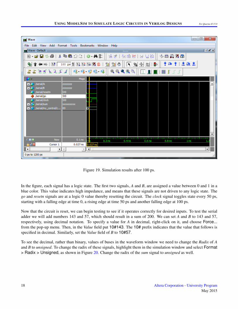
To run a simulation for 100 ps, set the value in the text field to 100 ps and press the Run button. After the simulationrun for 100 ps completes, you will see the state of the circuit as shown in Figure 19. You can change the time scaleof your waveform by going to View > Zoom > Zoom Range.... Change the end time to 1200 ps and press OK.
Altera Corporation - University ProgramMay 2015
17
USING MODELSIM TO SIMULATE LOGIC CIRCUITS IN VERILOG DESIGNS For Quartus II 15.0
Figure 19. Simulation results after 100 ps.
In the figure, each signal has a logic state. The first two signals, A and B, are assigned a value between 0 and 1 in ablue color. This value indicates high impedance, and means that these signals are not driven to any logic state. Thego and resetn signals are at a logic 0 value thereby resetting the circuit. The clock signal toggles state every 50 ps,starting with a falling edge at time 0, a rising edge at time 50 ps and another falling edge at 100 ps.
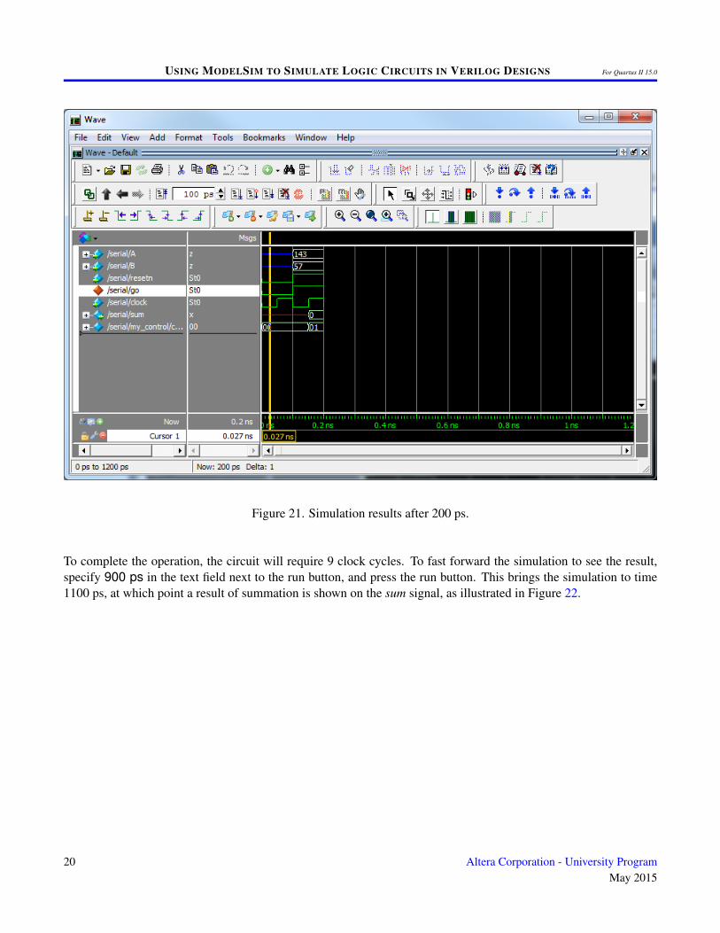
Now that the circuit is reset, we can begin testing to see if it operates correctly for desired inputs. To test the serialadder we will add numbers 143 and 57, which should result in a sum of 200. We can set A and B to 143 and 57,respectively, using decimal notation. To specify a value for A in decimal, right-click on it, and choose Force...from the pop-up menu. Then, in the Value field put 10#143. The 10# prefix indicates that the value that follows isspecified in decimal. Similarly, set the Value field of B to 10#57.
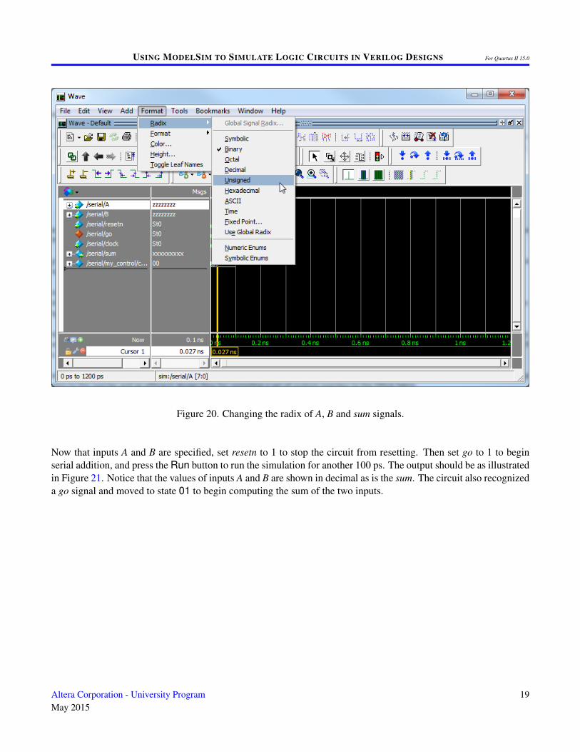
To see the decimal, rather than binary, values of buses in the waveform window we need to change the Radix of Aand B to unsigned. To change the radix of these signals, highlight them in the simulation window and select Format> Radix > Unsigned, as shown in Figure 20. Change the radix of the sum signal to unsigned as well.
18 Altera Corporation - University ProgramMay 2015
USING MODELSIM TO SIMULATE LOGIC CIRCUITS IN VERILOG DESIGNS For Quartus II 15.0
Figure 20. Changing the radix of A, B and sum signals.
Now that inputs A and B are specified, set resetn to 1 to stop the circuit from resetting. Then set go to 1 to beginserial addition, and press the Run button to run the simulation for another 100 ps. The output should be as illustratedin Figure 21. Notice that the values of inputs A and B are shown in decimal as is the sum. The circuit also recognizeda go signal and moved to state 01 to begin computing the sum of the two inputs.
Altera Corporation - University ProgramMay 2015
19
USING MODELSIM TO SIMULATE LOGIC CIRCUITS IN VERILOG DESIGNS For Quartus II 15.0
Figure 21. Simulation results after 200 ps.
To complete the operation, the circuit will require 9 clock cycles. To fast forward the simulation to see the result,specify 900 ps in the text field next to the run button, and press the run button. This brings the simulation to time1100 ps, at which point a result of summation is shown on the sum signal, as illustrated in Figure 22.
20 Altera Corporation - University ProgramMay 2015
USING MODELSIM TO SIMULATE LOGIC CIRCUITS IN VERILOG DESIGNS For Quartus II 15.0
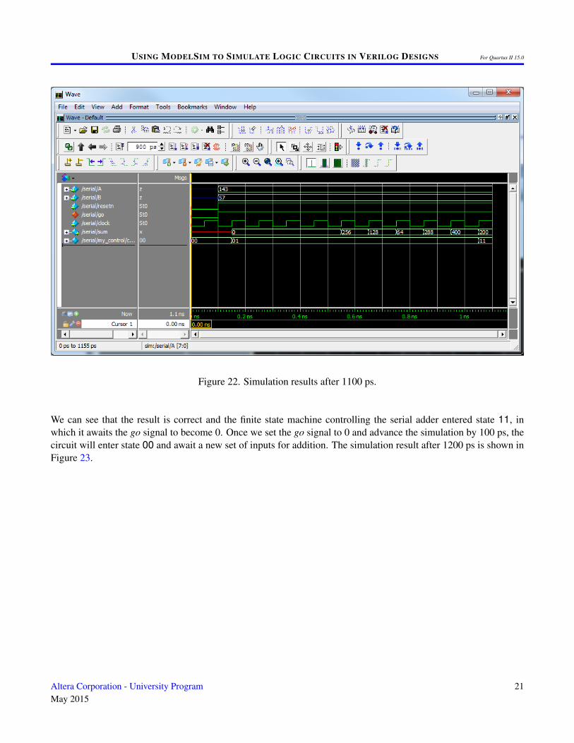
Figure 22. Simulation results after 1100 ps.
We can see that the result is correct and the finite state machine controlling the serial adder entered state 11, inwhich it awaits the go signal to become 0. Once we set the go signal to 0 and advance the simulation by 100 ps, thecircuit will enter state 00 and await a new set of inputs for addition. The simulation result after 1200 ps is shown inFigure 23.
Altera Corporation - University ProgramMay 2015
21
USING MODELSIM TO SIMULATE LOGIC CIRCUITS IN VERILOG DESIGNS For Quartus II 15.0
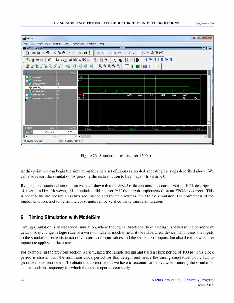
Figure 23. Simulation results after 1200 ps.
At this point, we can begin the simulation for a new set of inputs as needed, repeating the steps described above. Wecan also restart the simulation by pressing the restart button to begin again from time 0.
By using the functional simulation we have shown that the serial.v file contains an accurate Verilog HDL descriptionof a serial adder. However, this simulation did not verify if the circuit implemented on an FPGA is correct. Thisis because we did not use a synthesized, placed and routed circuit as input to the simulator. The correctness of theimplementation, including timing constraints can be verified using timing simulation.
5 Timing Simulation with ModelSim
Timing simulation is an enhanced simulation, where the logical functionality of a design is tested in the presence ofdelays. Any change in logic state of a wire will take as much time as it would on a real device. This forces the inputsto the simulation be realistic not only in terms of input values and the sequence of inputs, but also the time when theinputs are applied to the circuit.
For example, in the previous section we simulated the sample design and used a clock period of 100 ps. This clockperiod is shorter than the minimum clock period for this design, and hence the timing simulation would fail toproduce the correct result. To obtain the correct result, we have to account for delays when running the simulationand use a clock frequency for which the circuit operates correctly.
22 Altera Corporation - University ProgramMay 2015
USING MODELSIM TO SIMULATE LOGIC CIRCUITS IN VERILOG DESIGNS For Quartus II 15.0
For Altera FPGA-based designs the delay information is available after the design is synthesized, placed and routed,and is generated by Quartus II CAD software. The project for this part of the tutorial has been created for you in theexample/timing subdirectory; it has been configured to work with the DE2-115 board.
5.1 Setting up a Quartus II Project for Timing Simulation with ModelSim
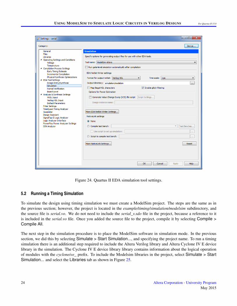
To perform timing simulation we need to set up Quartus II software to generate the necessary delay information forModelSim by setting up EDA Tools for simulation in the Quartus II project. To set up EDA Tools for simulation,open the Quartus II project in example/timing subdirectory, and select Assignment > Settings.... A window shownin Figure 24 will appear.
The window in the figure consists of a list on the left-hand side to select the settings category and a window areaon the right-hand side that displays the settings for a given category. Select Simulation from the EDA Tool Settingscategory to see the screen shown on the right-hand side of Figure 24.
The right-hand side of the figure contains the tool name at the top, EDA Netlist Writer settings in the middle, andNativeLink settings at the bottom. The tool name is a drop-down list containing the names of simulation tools forwhich Quartus II can produce a netlist with timing information automatically. This list contains many well-knownsimulation tools, including ModelSim. From the drop-down list select ModelSim-Altera.
Once a simulation tool is selected, EDA Netlist Writer settings become available. These settings configure QuartusII to produce input for the simulation tool. Quartus II will use these parameters to describe an implemented designusing a given HDL language, and annotate it with delay information obtained after compilation. The settings we candefine are the HDL language, simulation time scale that defines time step size for the simulator to use, the locationwhere the writer saves design and delay information, and others. Set these settings to match those shown in Figure 24and click OK.
With the EDA Tools Settings specified, we can proceed to compile the project in Quartus II. The compilation processsynthesizes, places, and routes the design, and performs timing analysis. Then it stores the compilation result in thesimulation directory for ModelSim to use. Take a moment to examine the files generated for simulation using a texteditor. The two main files are serial.vo, and serial_v.sdo.
The serial.vo file is a Verilog file for the design. The file looks close to the original Verilog file, except that thedesign now contains a wide array of modules with a cycloneive_ prefix. These modules describe resources on anAltera Cyclone IV E FPGA, on which the design was implemented using lookup tables, flip-flops, wires and I/Oports. The list of delays for each module instance in the design is described in the serial_v.sdo file.
Altera Corporation - University ProgramMay 2015
23
USING MODELSIM TO SIMULATE LOGIC CIRCUITS IN VERILOG DESIGNS For Quartus II 15.0
Figure 24. Quartus II EDA simulation tool settings.
5.2 Running a Timing Simulation
To simulate the design using timing simulation we must create a ModelSim project. The steps are the same as inthe previous section; however, the project is located in the example/timing/simulation/modelsim subdirectory, andthe source file is serial.vo. We do not need to include the serial_v.sdo file in the project, because a reference to itis included in the serial.vo file. Once you added the source file to the project, compile it by selecting Compile >Compile All.
The next step in the simulation procedure is to place the ModelSim software in simulation mode. In the previoussection, we did this by selecting Simulate > Start Simulation..., and specifying the project name. To run a timingsimulation there is an additional step required to include the Altera Verilog library and Altera Cyclone IV E devicelibrary in the simulation. The Cyclone IV E device library library contains information about the logical operationof modules with the cycloneive_ prefix. To include the Modelsim libraries in the project, select Simulate > StartSimulation... and select the Libraries tab as shown in Figure 25.
24 Altera Corporation - University ProgramMay 2015
USING MODELSIM TO SIMULATE LOGIC CIRCUITS IN VERILOG DESIGNS For Quartus II 15.0
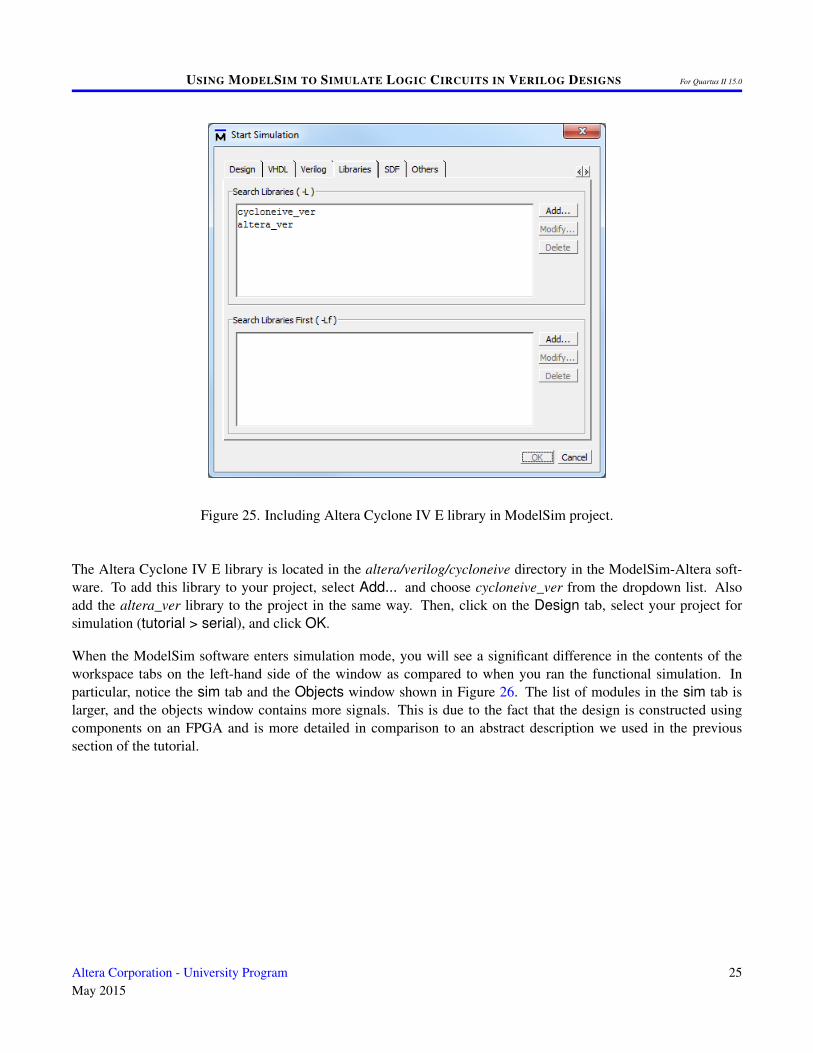
Figure 25. Including Altera Cyclone IV E library in ModelSim project.
The Altera Cyclone IV E library is located in the altera/verilog/cycloneive directory in the ModelSim-Altera soft-ware. To add this library to your project, select Add... and choose cycloneive_ver from the dropdown list. Alsoadd the altera_ver library to the project in the same way. Then, click on the Design tab, select your project forsimulation (tutorial > serial), and click OK.
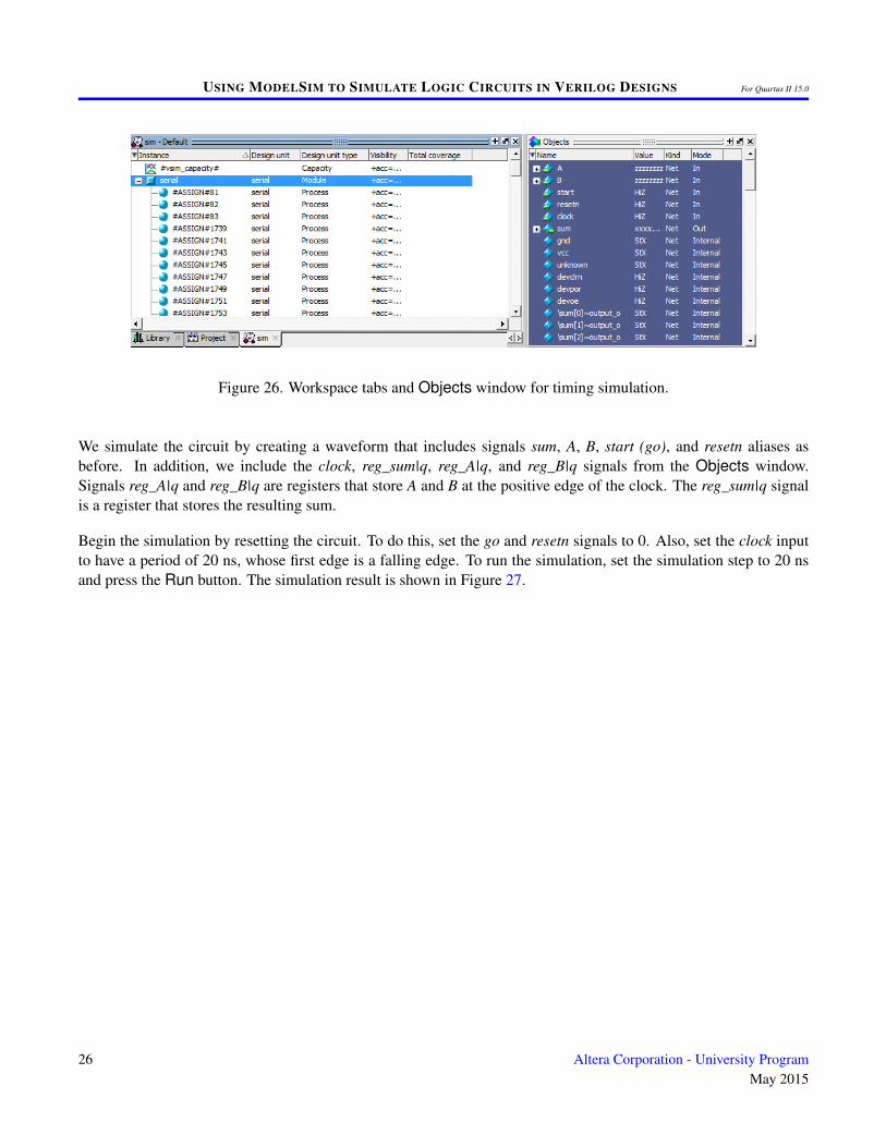
When the ModelSim software enters simulation mode, you will see a significant difference in the contents of theworkspace tabs on the left-hand side of the window as compared to when you ran the functional simulation. Inparticular, notice the sim tab and the Objects window shown in Figure 26. The list of modules in the sim tab islarger, and the objects window contains more signals. This is due to the fact that the design is constructed usingcomponents on an FPGA and is more detailed in comparison to an abstract description we used in the previoussection of the tutorial.
Altera Corporation - University ProgramMay 2015
25
USING MODELSIM TO SIMULATE LOGIC CIRCUITS IN VERILOG DESIGNS For Quartus II 15.0
Figure 26. Workspace tabs and Objects window for timing simulation.
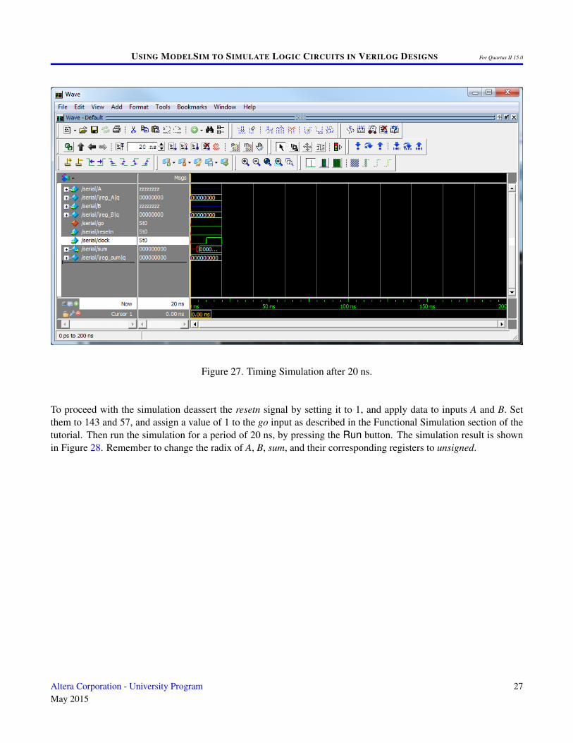
We simulate the circuit by creating a waveform that includes signals sum, A, B, start (go), and resetn aliases asbefore. In addition, we include the clock, reg_sum|q, reg_A|q, and reg_B|q signals from the Objects window.Signals reg_A|q and reg_B|q are registers that store A and B at the positive edge of the clock. The reg_sum|q signalis a register that stores the resulting sum.
Begin the simulation by resetting the circuit. To do this, set the go and resetn signals to 0. Also, set the clock inputto have a period of 20 ns, whose first edge is a falling edge. To run the simulation, set the simulation step to 20 nsand press the Run button. The simulation result is shown in Figure 27.
26 Altera Corporation - University ProgramMay 2015
USING MODELSIM TO SIMULATE LOGIC CIRCUITS IN VERILOG DESIGNS For Quartus II 15.0
Figure 27. Timing Simulation after 20 ns.
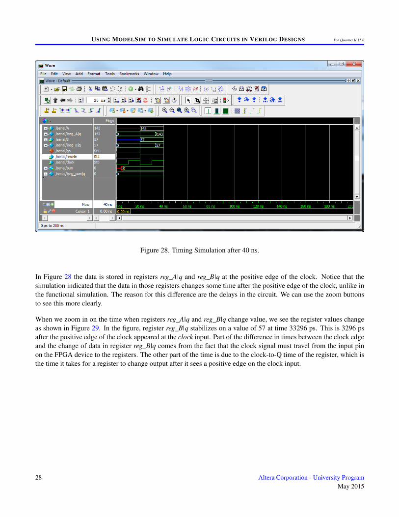
To proceed with the simulation deassert the resetn signal by setting it to 1, and apply data to inputs A and B. Setthem to 143 and 57, and assign a value of 1 to the go input as described in the Functional Simulation section of thetutorial. Then run the simulation for a period of 20 ns, by pressing the Run button. The simulation result is shownin Figure 28. Remember to change the radix of A, B, sum, and their corresponding registers to unsigned.
Altera Corporation - University ProgramMay 2015
27
USING MODELSIM TO SIMULATE LOGIC CIRCUITS IN VERILOG DESIGNS For Quartus II 15.0
Figure 28. Timing Simulation after 40 ns.
In Figure 28 the data is stored in registers reg_A|q and reg_B|q at the positive edge of the clock. Notice that thesimulation indicated that the data in those registers changes some time after the positive edge of the clock, unlike inthe functional simulation. The reason for this difference are the delays in the circuit. We can use the zoom buttonsto see this more clearly.
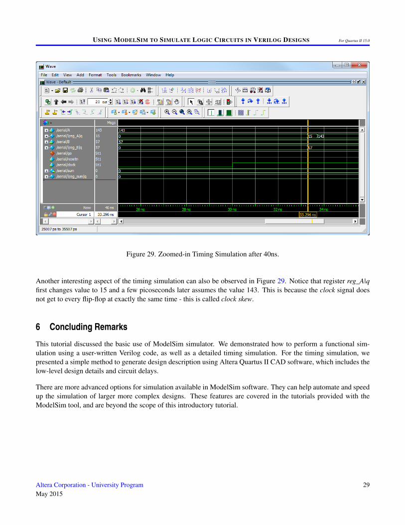
When we zoom in on the time when registers reg_A|q and reg_B|q change value, we see the register values changeas shown in Figure 29. In the figure, register reg_B|q stabilizes on a value of 57 at time 33296 ps. This is 3296 psafter the positive edge of the clock appeared at the clock input. Part of the difference in times between the clock edgeand the change of data in register reg_B|q comes from the fact that the clock signal must travel from the input pinon the FPGA device to the registers. The other part of the time is due to the clock-to-Q time of the register, which isthe time it takes for a register to change output after it sees a positive edge on the clock input.
28 Altera Corporation - University ProgramMay 2015
USING MODELSIM TO SIMULATE LOGIC CIRCUITS IN VERILOG DESIGNS For Quartus II 15.0
Figure 29. Zoomed-in Timing Simulation after 40ns.
Another interesting aspect of the timing simulation can also be observed in Figure 29. Notice that register reg_A|qfirst changes value to 15 and a few picoseconds later assumes the value 143. This is because the clock signal doesnot get to every flip-flop at exactly the same time - this is called clock skew.
6 Concluding Remarks
This tutorial discussed the basic use of ModelSim simulator. We demonstrated how to perform a functional sim-ulation using a user-written Verilog code, as well as a detailed timing simulation. For the timing simulation, wepresented a simple method to generate design description using Altera Quartus II CAD software, which includes thelow-level design details and circuit delays.
There are more advanced options for simulation available in ModelSim software. They can help automate and speedup the simulation of larger more complex designs. These features are covered in the tutorials provided with theModelSim tool, and are beyond the scope of this introductory tutorial.
Altera Corporation - University ProgramMay 2015
29
USING MODELSIM TO SIMULATE LOGIC CIRCUITS IN VERILOG DESIGNS For Quartus II 15.0
Copyright ©1991-2015 Altera Corporation. All rights reserved. Altera, The Programmable Solutions Company, thestylized Altera logo, specific device designations, and all other words and logos that are identified as trademarksand/or service marks are, unless noted otherwise, the trademarks and service marks of Altera Corporation in theU.S. and other countries. All other product or service names are the property of their respective holders. Alteraproducts are protected under numerous U.S. and foreign patents and pending applications, mask work rights, andcopyrights. Altera warrants performance of its semiconductor products to current specifications in accordance withAltera’s standard warranty, but reserves the right to make changes to any products and services at any time withoutnotice. Altera assumes no responsibility or liability arising out of the application or use of any information, product,or service described herein except as expressly agreed to in writing by Altera Corporation. Altera customers areadvised to obtain the latest version of device specifications before relying on any published information and beforeplacing orders for products or services.
This document is being provided on an ”as-is” basis and as an accommodation and therefore all warranties, repre-sentations or guarantees of any kind (whether express, implied or statutory) including, without limitation, warrantiesof merchantability, non-infringement, or fitness for a particular purpose, are specifically disclaimed.
30 Altera Corporation - University ProgramMay 2015


![Writing a Testbench in Verilog & Using Modelsim to … - Introduction to Digital Circuits Testbenches & Modelsim Experiment ee254_testbench.fm [Revised: 7/20/14] 1/19 Writing a Testbench](https://img.pdfslide.us/doc/110x75/5aa26d797f8b9a1f6d8d3a2b/writing-a-testbench-in-verilog-using-modelsim-to-introduction-to-digital-circuits.jpg)