Embed Size (px)
Citation preview
University of Illinois
Non-linear Electrodynamic Responseof Dielectric Materials
microwave applications (radar, etc)phase shifterstuned filtersvoltage controlled oscillators
optical applications (wdm, etc)amplitude modulatorsphase modulatorsfrequency shifters
these things are cm longbetter to be microns long!
PowerPoint Presentation by: Professor Jim EcksteinDepartment of Electrical and Computer Engineering
University of Illinois
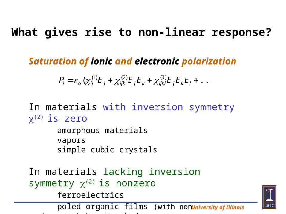
What gives rise to non-linear response?
Saturation of ionic and electronic polarization
In materials with inversion symmetry (2) is zeroamorphous materialsvaporssimple cubic crystals
In materials lacking inversion symmetry (2) is nonzeroferroelectrics
poled organic films (with non-centrosymmetric molecules)
....)( )3()2()1( lkjijklkjijkjijoi EEEEEEP
P
E
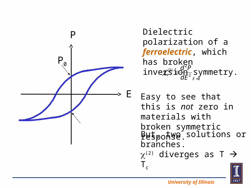
Dielectric polarization of a ferroelectric, which has broken inversion symmetry.
02
2)2(
Ee dE
Pd
Easy to see that this is not zero in materials with broken symmetric response.
But, two solutions or branches.(2) diverges as T Tc
University of Illinois
P0

P
E
For non-linear optical and other field tuning applications would prefer a characteristic like this.
Stable, single solutioncan’t de-pole
Permanently polarized dielectric with big (2)
Use molecular nanostructuring to make such a material (MBE)(once you figure out what matters!)
University of Illinois
What you would like for non-linear modulators, etc…
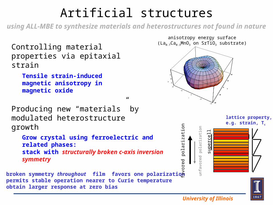
Artificial structuresusing ALL-MBE to synthesize materials and heterostructures not found in nature
• broken symmetry throughout film favors one polarization• permits stable operation nearer to Curie temperature• obtain larger response at zero bias
Grow crystal using ferroelectric and related phases:stack with structurally broken c-axis inversion symmetry
lattice property, e.g. strain, Tc
favo
red
po
lariz
atio
n
unfa
vore
d po
lariz
atio
n
sup
erc
ell
Controlling material properties via epitaxial strain
Producing new “materials” by modulated heterostructure growth
Tensile strain-induced magnetic anisotropy in magnetic oxide
-20
-10
0
10
20
X
-20
-10
0
10
20
Y
-5
0
5
Z
-20
-10
0
10
20
X
-5
0
5
Z
anisotropy energy surface(La0.7Ca0.3MnO3 on SrTiO3 substrate)
University of Illinois

University of Illinois
Introducing the actors , perovskite titanate phases
BaTiO3
ferroelectric (order-disorder, weakly 1st order)
SrTiO3
non ferroelectric, but would like to bewell known substrate
CaTiO3
ferroelectricity, what’s that??
4.0 A
3.9 A
3.8 A
Combine these in single crystal heterostructures to investigate the effects of compositional (strain) symmetry breaking
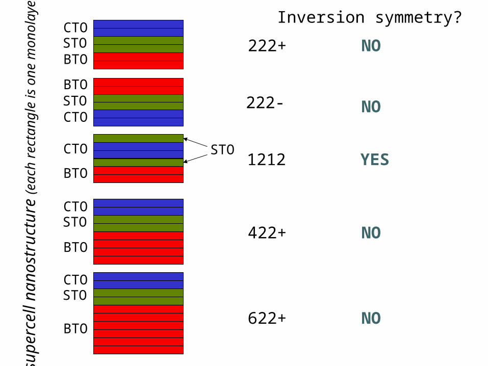
Inversion symmetry?CTOSTOBTO
222+ NO
STOBTO
CTO222- NO
CTO STO
BTO1212 YES
CTOSTO
BTO422+ NO
CTOSTO
BTO622+ NO
supe
rcel
l nan
ostr
uctu
re (e
ach
rect
angl
e is
one
mon
olay
er)

Atomic Layer-by-Layer Molecular Beam Epitaxy
OzonegeneratorO
xyg
en
Pump
Ca
Sr
Ba
Al
La
Y
Ti
Mn
Cu
Bi
rotating substrate positioner
quartzcrystalmonitor
RHEED
electrongun
hollowcathode
lamp
photomultipliertube quadrupole
massspectrometer
turbopump
loadlock
shutters
hollowcathode
lamp
photomultipliertube
substrateholder
• atomic absorption spectroscopy for feedback control
• ozone oxidation
• in-situ RHEED with digital video
• We have control over the source fluxes to better than 1% accuracy (AA, RHEED)
ozonestill
RHEED reveals surface crystal structure
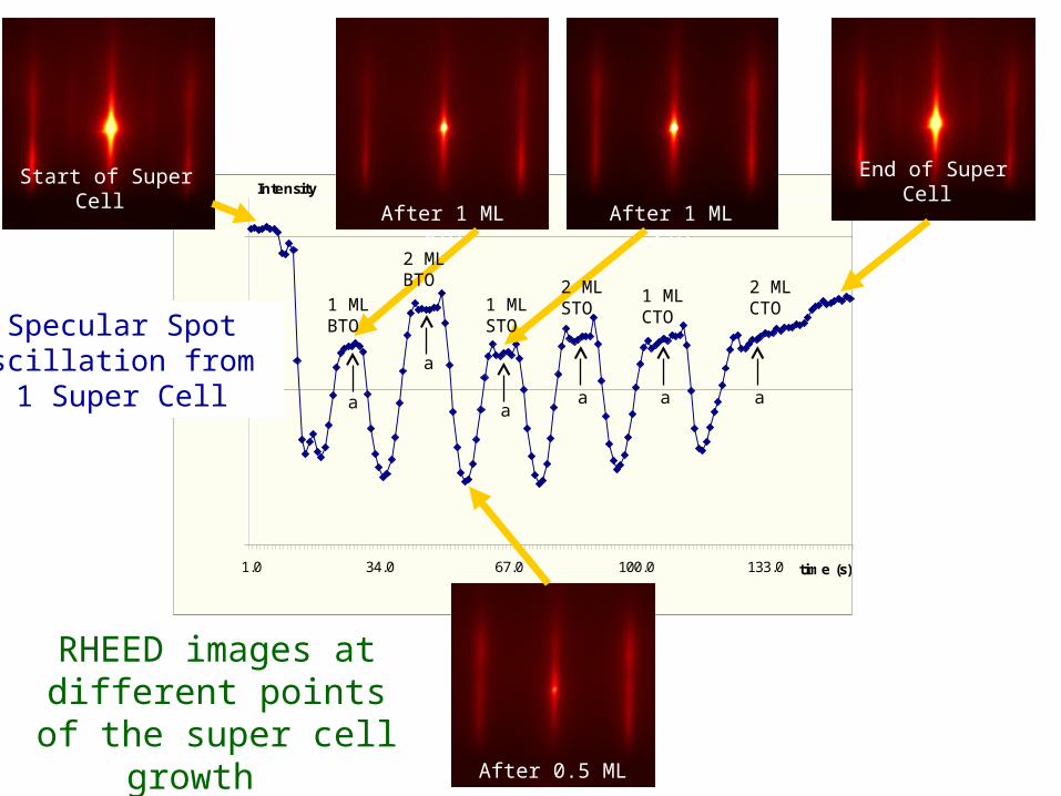
1.0 34.0 67.0 100.0 133.0 time (s)
Intensity
a
a
aa a a
RHEED images at different points of the
super cell growth
Start of Super Cell
CTO Surface
End of Super Cell
CTO SurfaceAfter 1 ML BTO After 1 ML STO
After 0.5 ML STO
Specular SpotOscillation from
1 Super Cell
1 ML BTO
2 ML BTO
1 ML STO
2 ML STO
1 ML CTO
2 ML CTO
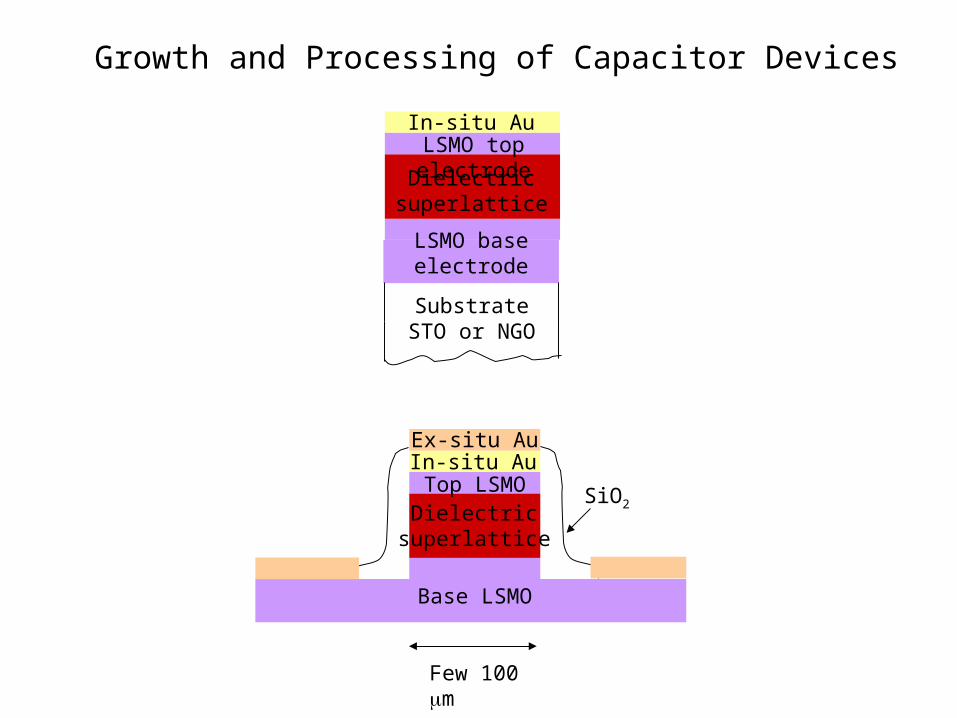
Growth and Processing of Capacitor Devices
SubstrateSTO or NGO
Dielectric superlattice
LSMO base electrode
LSMO top electrodeIn-situ Au
In-situ AuTop LSMO
Ex-situ Au
Dielectric superlattice
Base LSMO
SiO2
Few 100 m
University of Illinois
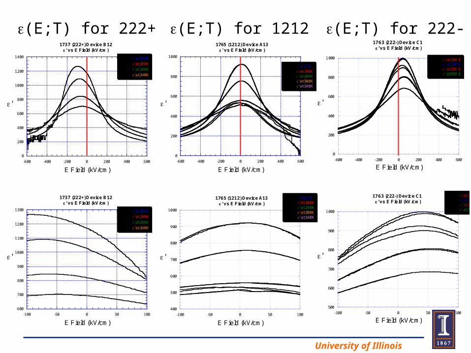
400
500
600
700
800
900
1000
-100 -50 0 50 100
1765 (1212) Device A13' vs E Field (kV/cm)
' at 25K' at 100K' at 200K' at 300K' at 340K
'
E Field (kV/cm)
600
700
800
900
1000
1100
1200
1300
-100 -50 0 50 100
1737 (222+) Device B12' vs E Field (kV/cm)
' at 100K
' at 200K
' at 280K
' at 340K
'
E Field (kV/cm)
500
600
700
800
900
1000
-100 -50 0 50 100
1763 (222-) Device C1 ' vs E Field (kV/cm)
' at 100 K' at 160 K' at 280 K' at 340 K
'
E Field (kV/cm)
0
200
400
600
800
1000
1200
1400
-600 -400 -200 0 200 400 600
1737 (222+) Device B12' vs E Field (kV/cm)
' at 100K
' at 200K
' at 280K
' at 340K
'
E Field (kV/cm)
(E;T) for 222+
0
200
400
600
800
1000
-600 -400 -200 0 200 400 600
1765 (1212) Device A13' vs E Field (kV/cm)
' at 25K' at 100K' at 200K' at 300K' at 340K
'
E Field (kV/cm)
(E;T) for 1212
0
200
400
600
800
1000
-600 -400 -200 0 200 400 600
1763 (222-) Device C1 ' vs E Field (kV/cm)
' at 100 K' at 160 K' at 280 K' at 340 K
'
E Field (kV/cm)
(E;T) for 222-
University of Illinois
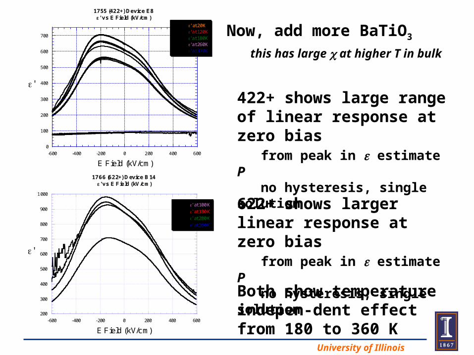
Now, add more BaTiO3
this has large at higher T in bulk
0
100
200
300
400
500
600
700
-600 -400 -200 0 200 400 600
1755 (422+) Device E8' vs E Field (kV/cm)
' at 20K' at 120K' at 180K' at 260K' at 370K
'
E Field (kV/cm)
422+ shows large range of linear response at zero bias
from peak in estimate Pno hysteresis, single solution
200
300
400
500
600
700
800
900
1000
-600 -400 -200 0 200 400 600
1766 (622+) Device B14 ' vs E Field (kV/cm)
' at 100K
' at 180K
' at 280K
' at 360K
'
E Field (kV/cm)
622+ shows larger linear response at zero bias
from peak in estimate Pno hysteresis, single solution
Both show temperature indepen-dent effect from 180 to 360 K
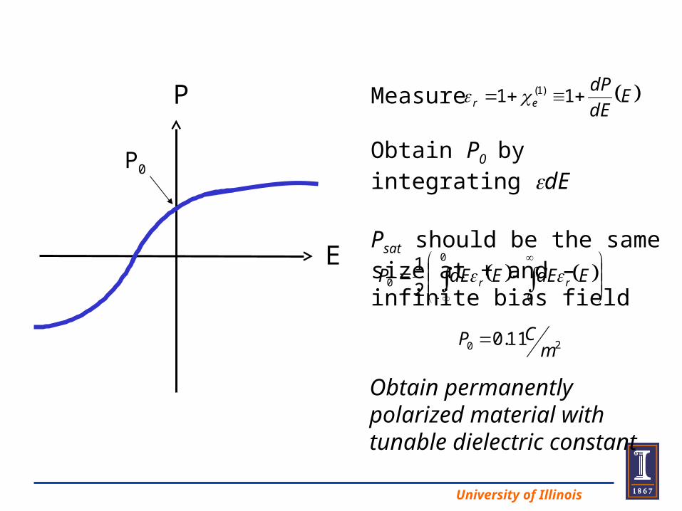
P
E
P0
Measure
Obtain P0 by integrating dE
Psat should be the same size at + and – infinite bias field
EdE
dPer 11 )1(
EdEEdEP rr 0
0
0 2
1
20 11.0m
CP
University of Illinois
Obtain permanently polarized material with tunable dielectric constant