Embed Size (px)
Citation preview

UNIVERSITY OF CALIFORNIA
SANTA CRUZ
ELECTROCHEMICAL DOPING AND THE OPTICAL PROPERTIES OF
LIGHT-EMITTING POLYMER MATERIALS AND DEVICES
A dissertation submitted in partial satisfaction
of the requirements for the degree of
DOCTOR OF PHILOSOPHY
in
PHYSICS
by
Janelle Maureen Leger
June 2005
The Dissertation of Janelle Maureen Leger
is approved:
Professor Sue Carter, Chair
Professor David Belanger
Professor Jin Zhang
Robert C. Miller
Vice Chancellor for Research and
Dean of Graduate Studies

Copyright ! by
Janelle Maureen Leger
2005

iii
TABLE OF CONTENTS
Page
LIST OF FIGURES vii
LIST OF TABLES xv
ABSTRACT xvi
ACKNOWLEDGEMENTS xix
INTRODUCTION 1
CHAPTER 1: POLYMERIC SEMICONDUCTORS
1.1 Origins of semiconductivity in conjugated polymers 5
1.2 Absorption and emission processes 9
1.3 Doping of semiconducting polymers 15
CHAPTER 2: OPTOELECTRONIC POLYMER DEVICES
2.1 Light-emitting diodes 22
2.2 Light-emitting electrochemical cells 29
2.3 Electrochromic devices 34
2.4 Interference in multilayered device structures 37
CHAPTER 3: EXPERIMENTAL TECHNIQUES
3.1 Cyclic voltammetry 41
3.2 Device construction 47
3.3 Measurement of photoluminescence and absorption spectra 49

iv
3.4 Atomic force microscopy (AFM) 51
3.5 Electronic characterization of devices 53
3.6 Optical characterization of devices 57
CHAPTER 4: THICKNESS DEPENDENCE AND INTERFERENCE
EFFECTS IN POLYMER LIGHT-EMITTING DIODE STRUCTURES
4.1 Abstract 62
4.2 Introduction 62
4.3 Experimental details and thickness-dependent results 64
4.4 Simulation of interference effects in PLED structures 69
4.5 Simulation of emission zone location 73
4.6 Conclusions 79
CHAPTER 5: RECOMBINATION PROFILES IN MEH-PPV LIGHT-
EMITTING ELECTROCHEMICAL CELLS
5.1 Abstract 80
5.2 Introduction 81
5.3 Experimental details 84
5.4 Planar geometry LECs 85
5.5 Simulating interference effects in vertical geometry LECs 89
5.6 Comparison of simulation and experiment: 92
EL spectra of MEH-PPV LECs
5.7 Electrical and optical characterization of vertical geometry LECs 98

v
5.8 Discussion and conclusions 103
CHAPTER 6: ELECTROCHEMICAL AND OPTICAL
CHARACTERIZATION OF p- AND n- DOPED MEH-PPV
6.1 Abstract 105
6.2 Introduction 106
6.3 Experimental details 108
6.4 Cyclic voltammetry results 111
6.5 Absorption spectra at progressive doping levels 118
6.6 Photoluminescence quenching 123
6.7 Conclusions 126
CHAPTER 7: SOLID-STATE ELECTROCHROMIC DEVICES BASED ON
PPV POLYMERS
7.1 Abstract 128
7.2 Introduction 128
7.3 Construction and characterization of MEH-PPV ECDs 129
7.4 Physical models for factors affecting device performance 132
7.5 Conclusions 136
CHAPTER 8: REVERSIBLE THERMOCHROMIC EFFECTS IN MEH-PPV
8.1 Abstract 137
8.2 Introduction 137
8.3 Experimental details 139

vi
8.4 Results and discussion 140
8.5 Conclusions 144
BIBLIOGRAPHY 145

vii
LIST OF FIGURES
CHAPTER 1: POLYMERIC SEMICONDUCTORS
1.1 Energy bands in an insulator, semiconductor, and conductor (p.6).
1.2 The molecular structure and molecular orbitals of polyacetylene (p.7).
1.3 Energy level splitting of orbitals in a conjugated polymer according to
molecular orbital theory (p.9).
1.4 Potential energy as a function of internuclear distance for the ground and first
excited states of a diatomic molecule (p.11).
1.5 Examples of absorption and emission spectra, Stokes shift, and spectral
overlap (p.12).
1.6 Exciton formation from a) photoexcitation and b) injected carriers (p.13).
1.7 Pathways for recombination of a singlet exciton in a conjugated polymer
(p.14).
1.8 Amorphous polymer in thin film form (p.15).
1.9 Molecular structure of the PPV repeat unit in (a) benzoid (non-doped) and (b)
quinoid (doped) form (p.16).
1.10 Energy levels of a conjugated polymer in (a) neutral form, with conduction
and valence bands only, (b) lightly doped, with the addition of a single bipolaron
energy level, and (c) more heavily doped, with a broad bipolaron band (p.18).
viii
1.11 The formation of polaron and bipolaron defects in a conjugated polymer
(p.19).
1.12 Energetic structure of a material with polaron and bipolaron defects and
allowed electronic transitions (p.20).
CHAPTER 2: OPTOELECTRONIC POLYMER DEVICES
2.1 Lattice structure and energy band diagram for (a) p-type and (b) n-type
crystalline semiconductor (p.23).
2.2 Formation of a p-n junction (p.24).
2.3 Polymer LED device structure with Ca/Al cathode and PEDOT-PSS/ITO
anode (p.26).
2.4 An example of an energy level/ work function diagram for a PLED (p.26).
2.5 Schematic diagram of a PLED in forward bias illustrating the charge injection,
transport, and recombination processes (p.27).
2.6 Two proposed methods for charge injection in a PLED include a) Fowler-
Nordheim tunneling and b) thermionic injection (p.28).
2.7 A typical LEC device structure (p.30).
2.8 Proposed operating mechanism for an LEC (p.32).
2.9 Alternate proposed mechanism for LEC operation (p.33).
2.10 A typical ECD device structure (p.36).

ix
2.11 Wide-angle and multiple-beam interference effects in polymer light-emitting
devices (p.38).
CHAPTER 3: EXPERIMENTAL TECHNIQUES
3.1 Typical 3-electrode electrochemical cell (with film sample) used in cyclic
voltammetry experiments (p.42).
3.2 Triangular waveform generated by the potentiostat in a typical cyclic
voltammetry experiment (p.44).
3.3 Basic potentiostat layout (p.44).
3.4 Experimental setup for cyclic voltammetry (p.45).
3.5 A voltammogram of an ideal system in forward scan (p.46).
3.6 Polymer light-emitting device geometry at various stages of construction
(p.48).
3.7 Brief schematic of the instrument used to measure the fraction of light
transmitted through a film sample (p.50).
3.8 Brief schematic of the instrument used to measure the photoluminescence of
(a) dilute solution and (b) film sample (p.51).
3.9 The basic operating mechanism of the atomic force microscope (AFM) (p.52).
3.10 The profile of a polymer film during a thickness measurement (p.53).
3.11 Example I-V curve for a polymer LED (p.55).
3.12 Example I-V curve for a polymer LEC (p.56).

x
3.13 Example I-V curve for a polymer ECD (p.57).
3.14 A representative plot of external quantum efficiency as a function of applied
voltage for a polymer LED (p.59).
3.15 The C.I.E. chromaticity diagram (p.61).
3.16 The C.I.E. color matching functions (p.61).
CHAPTER 4: THICKNESS DEPENDENCE AND INTERFERENCE EFFECTS
IN POLYMER LIGHT-EMITTING DIODE STRUCTURES
4.1 Normalized film absorption, solution PL, and film PL for (a) MEH-DOO-PPV
and (b) PF. Inlays show the chemical structures for each polymer (p.66).
4.2 Normalized EL spectra for (a) MEH-DOO-PPV, with thicknesses 55 nm, 62
nm, 86 nm, and 100 nm and (b) PF, with thicknesses 135 nm, 151 nm, 186 nm, and
213 nm (p.68).
4.3 Refractive index dispersion curves for MEH-DOO-PPV and PF (p.70).
4.4 Simulated normalized EL spectra for (a) MEH-DOO-PPV, and (b) PF, with
various thicknesses (p.71).
4.5 Experimental and simulated radiance curves in arbitrary units, for (a) MEH-
DOO-PPV and (b) PF. For the simulated results, emission is assumed to occur 20%
of device thickness away from the anode (p.73).
4.6 Simulated normalized EL spectra for single device thickness as a function of
emission zone for (a) 100nm MEH-DOO-PPV device, with emission occurring at 10

xi
nm, 30 nm, 70 nm, and 90 nm from anode, and (b) 190 nm PF device, with emission
occurring at 38 nm, 76 nm, 114 nm, and 152 nm from anode (p.77).
4.7 Simulated normalized EL spectra for (a) MEH-DOO-PPV, with thicknesses
55 nm, 62 nm, 86 nm, and 100 nm and emission assumed to occur 70% of device
thickness away from the anode, and (b) PF, with thicknesses 130 nm, 150 nm, 190
nm, and 210 nm, and emission assumed to occur 80% of device thickness away from
the anode (p.78).
CHAPTER 5: RECOMBINATION PROFILES IN MEH-PPV LIGHT-EMITTING
ELECTROCHEMICAL CELLS
5.1 Device structure of a planar geometry light-emitting electrochemical cell
(p.86).
5.2 The 0 V photoluminescence, 3 V photoluminescence, and 10 V
electroluminescence of a planar LEC with TBABF4 salt (p.87).
5.3 Optical constants n and k of a thin film of MEH-PPV:PEO (p.91).
5.4 Experimental and simulated EL spectra of a 500 nm device with Au top
electrodes in forward and reverse bias (p.93).
5.5 Experimental and simulated EL spectra of a 300 nm device with Al top
electrodes in forward and reverse bias (p.94).
5.6 Experimental and simulated EL spectra of a 250 nm device with Au top
electrodes in forward and reverse bias (p.95).

xii
5.7 Experimental and simulated EL spectra of a 250 nm device with Au top
electrodes in high and low reverse bias (p.96).
5.8 Simulated EL spectra of a 300 nm device with Al top electrodes as a function
of emission location throughout the polymer layer (p.97).
5.9 Current-voltage curves for LECs using Li triflate and both Au and Al top
electrodes. Devices were first charged at high positive or negative voltages prior to
voltage sweep (p.99).
5.10 Radiance-voltage curves for devices using Li triflate and Au or Al top
electrodes (p.102).
5.11 Radiance-voltage curves for devices using various salts and Au top electrodes
(p.102).
CHAPTER 6: ELECTROCHEMICAL AND OPTICAL CHARACTERIZATION
OF p- AND n- DOPED MEH-PPV
6.1 MEH-PPV chemical structure, absorbtance spectra, and photoluminescence
spectra for film and solution (p.109).
6.2 Cyclic voltammetry setup and cyclic voltammagrams for various MEH-PPV
working electrodes with a) 0.01 M Li triflate and b) 0.01 M TBA BF4 electrolyte.
(p.113).
6.3 Cyclic Voltammogram for MEH-PPV at varied scan rates in 0.01 M Li triflate
electrolyte (p.115).

xiii
6.4 Cyclic voltammograms for MEH-PPV for a) different film thicknesses and b)
varied salt concentration (p.117).
6.5 Illustration of the energy transitions for a) an undoped polymer, b) a positive
polaron and c) and positive bipolaron (p.118).
6.6 Absorptance spectra for an MEH-PPV film at progressive doping levels
(p.120).
6.7 Illustration of bipolaron energy levels in MEH-PPV (p.120).
6.8 In situ obtained absorbtance spectra of n-doped MEH-PPV film (p.122).
6.9 Photoluminescence spectra for MEH-PPV film at progressive oxidative
doping levels (p.124).
6.10 Photoluminescence spectra for MEH-PPV film at progressive reductive
doping levels (p.125).
CHAPTER 7: SOLID-STATE ELECTROCHROMIC DEVICES BASED ON PPV
POLYMERS
7.1 ECD structure, MEH-PPV chemical structure, and the absorbance spectra for
an undoped device (0 Volts) in comparison with that of a fully doped device (2 Volts)
(p.132).
7.2 The dependence of the optical contrast of a solid state device at 700 nm on a)
device thickness with a concentration of 0.07 M of TBA PF6, b) salt type each at 0.65
M, and c) salt concentration measured in weight percentage of Li triflate (p.134).

xiv
7.3 Cyclic voltammograms normalized at the anodic peak taken at 20 mV/s for
varying salt concentrations from 2.5 mM to 40 mM (p.136).
CHAPTER 8: REVERSIBLE THERMOCHROMIC EFFECTS IN MEH-PPV
8.1 MEH-PPV gel films at increasing temperatures (p.141).
8.2 Temperature-dependent absorption spectra for MEH-PPV (p.142).
8.3 Temperature dependence of HOMO/LUMO energy levels in MEH-PPV
(p.143).
xv
LIST OF TABLES
CHAPTER 6: ELECTROCHEMICAL AND OPTICAL CHARACTERIZATION
OF p- AND n- DOPED MEH-PPV
6.1 Doping onset potentials, calculated HOMO/LUMO levels, electrochemical
bandgap, and qualitative reversibility for MEH-PPV on various electrodes (p.114).

ABSTRACT
ELECTROCHEMICAL DOPING AND THE OPTICAL PROPERTIES OF LIGHT-
EMITTING POLYMER MATERIALS AND DEVICES
Janelle Leger
The discovery in 1990 by Bradley et. al. that organic polymers with a
conjugated backbone display semiconducting properties began an intensive research
effort to understand the fundamental physics underlying these materials, to synthesize
materials with certain desired properties, and to develop potential applications.
Specifically, semiconducting polymers have been used in a wide range of device
applications including light-emitting devices, transistors, photovoltaics, memory
devices, and actuators, among others. The promising characteristics of polymer
semiconductors include low-cost, easy processing, tailored synthesis, and potential
for use in large-area and flexible devices.
In this dissertation I introduce the field of semiconducting polymers and
present my studies of electrochemical doping and the optical properties of light-
emitting polymers in the context of improving functionality in a range of solid-state
device applications. While great strides have been made toward the practical
realization of a range of polymer-based optoelectronic and electronic applications,

there is still much to learn about the fundamental processes affecting their optical
properties. Specifically, detailed studies of the electrochemical doping of light-
emitting polymers are lacking despite the emergence of a range of technologies such
as polymer light-emitting electrochemical cells that depend heavily on the process of
in situ electrochemical doping. In addition, the factors affecting the optical properties
of light-emitting polymers and polymer-based devices have been limited in scope.
The first three chapters of this dissertation serve as an introduction to the field
of light-emitting polymers and polymer-based devices including materials, device
construction, and measurement techniques. In chapter one I discuss the physical
models necessary to understand semiconductivity in conjugated polymers. Chapter
two reviews the device physics of several important applications. In chapter three I
introduce the experimental techniques used in the following studies.
Two well established light-emitting polymer devices include the polymer
LED and the polymer LEC. The LEC uses electrochemical doping to achieve the
charge injection necessary for light emission, while the LED injects charge directly
from contact electrodes. I use a technique employing simulations of interference
effects in multilayered device structures, matching experimental device spectra to
simulation in order to gain insight into the location of light emission within the
device. In chapter four I use this technique to explore the thickness dependence of
PLEDs. In chapter five I combine simulations of interference effects in LECs with

studies of planar geometry devices, thereby providing information about the
fundamental operating mechanism of these devices.
Several polymer-based applications include light-emitting electrochemical
cells (LEC), electrochromic devices (ECD), and actuators, for which the operating
mechanism depends heavily on electrochemical doping. Unfortunately, the doping of
light-emitting polymers is not well understood. In chapter six I study the basic
electrochemical doping reactions of one common light-emitting polymer, MEH-PPV.
I explore factors affecting the fundamental doping reaction through cyclic
voltammetry. Further, I investigate the optical properties of doped films in order to
gain insight into the structural changes and changes in the energy band structure
induced by doping.
Finally, I explore some unique functionalities of MEH-PPV, specifically
electrochromic and thermochromic effects. Chapter seven presents a MEH-PPV
based electrochromic device with a layered polymer/gel electrolyte structure that
displays sharp contrast and high reversibility when biased at low operating voltages.
In chapter eight I study the reversible, high-contrast thermochromic behavior of
MEH-PPV gel films, occurring in a practically relevant temperature range and
without phase or volume changes.

xix
ACKNOWLEDGEMENTS
My name appearing alone on the first page of this work does not reflect the
enormous contributions of the following individuals, both directly and indirectly, to
the very existence of this manuscript. Most important is the thanks I owe to Sue
Carter, whose teaching, support, and encouragement I struggled to deserve until the
end. Amanda Holt and Beat Ruhstaller have contributed to a great extent directly to
the studies presented here and have been an absolute pleasure to work with.
Invaluable help has also come from other sources in the form of materials and other
assistance, in particular Luisa Bozano and Campbell Scott at IBM, who helped with
several measurements that were central to the work.
The text of this dissertation includes reprints of the following previously
published material: "Solid-state electrochromic devices based on poly (phenylene
vinylene) polymers", Appl. Phys. Lett. 86 (2005) and "Thickness-dependent changes
in the optical properties of PPV- and PF- based polymer light-emitting diodes", Phys.
Rev. B 68 (2003). Professor Sue Carter directed and supervised the research which
forms the basis for the dissertation.
Last but not least there are the people in my life who have supported me
endlessly. For friendship and camaraderie throughout my time at UCSC I want to
thank in particular Melissa Kreger and Yuko Nakazawa. I want to thank my father
for advice and support, and my mother for saving my sanity both as a graduate

xx
student and as a mother. Most of all, I dedicate this work to Eric, who has given me
love, unwavering support, and Kaia.

1
INTRODUCTION
The field of semiconducting polymers was born in 1977 when it was
discovered that polyacetylene, when chemically doped, exhibited a several orders of
magnitude increase in its electrical conductivity (Shirakawa et. al. 1977). By 1979,
Su, Schrieffer, and Heeger had proposed a theoretical model describing conductivity
in doped conjugated polymers (Su et. al. 1979), and a collection of new polymers had
been synthesized, including the luminescent polymer poly (p-phenylene) (PPP) (Ivory
et. al. 1979). Additionally, in 1979 it was discovered that these materials could also
be electrochemically doped to achieve a conductive state, and that this process was
reversible (Nigrey et. al. 1979).
In the 1980’s and 1990’s research focus tended to be on demonstrating the
usefulness of semiconducting and conducting polymers in a broad range of
applications. Organic field-effect transistors (Burroughes et. al. 1988),
electrochromic devices, actuators, and several other applications based on conjugated
polymers all made their appearance in the late 1980’s (MacDiarmid and Zheng 1997).
In 1990, electroluminescence from a light-emitting diode based on the luminescent
polymer poly (phenylenevinylene) (PPV) was demonstrated (Burroughes et. al.
1990). One year later, a polymer light-emitting diode was fabricated by spin-casting
a polymer film from the soluble PPV derivative, poly [2-methoxy-5-(2-
ethylhexyloxy)-1,4-phenylenevinylene)] (MEH-PPV) (Braun and Heeger 1991). In

2
the mid-1990’s the polymer photovoltaic cell (Yu et. al. 1994, Brabec et. al. 2001)
and the polymer light-emitting electrochemical cell (Pei et. al. 1995) were reported.
The heavy research effort and exploding application development in the field
of polymer semiconductor materials and devices in the past 28 years is indicative of
the potential of these materials in a wide range of applications (Epstein 1997). For
example, their synthetic process allows for easy tunability of their optical and
electronic properties. In comparison with traditional crystalline semiconductors, the
ease of processing of conjugated polymers is vastly improved, promising significant
cost advantages over current technologies. Perhaps the most significant benefit,
however, comes from the liquid processing capabilities of polymers. This opens up
the possibility of making large area, mechanically flexible devices on a wide range of
substrates including plastic, paper, or even textiles (Forrest 2004). In addition, film
deposition can be accomplished by cheap, efficient processes such as ink-jet printing,
screen-printing, and others that will allow roll-to-roll production of technologies such
as all-polymer displays.
Currently the field of organic electronic devices has reached the performance
and stability necessary to achieve commercial production for a few applications. The
introduction of organic devices into commercial production has shifted research focus
somewhat from reaching certain performance and stability requirements to tuning
material and device properties to certain specific applications. For example,
multicolored displays fabricated using PLEDs will require a detailed understanding of

3
how the spectral properties of a device are affected by device construction and
operating parameters. In this work I explore how the optical properties of LEPs are
affected by such parameters as temperature and electrochemical doping for thin films,
and device thickness and operating voltage, among others, through the study of
optical interference effects in solid-state device applications.
Despite meeting the basic requirements for limited commercial production,
several problems of short- and long-term efficiency continue to limit polymer device
fabrication. In particular, stability is a major limitation of polymer device lifetimes.
The polymers themselves are particularly sensitive to exposure to oxygen, moisture,
and UV radiation. Further, some polymer device applications require the use of
reactive high work function electrodes. These environmental instabilities of polymer
devices demand highly effective encapsulation techniques for long-term device
operation, reducing ease of production and low-cost benefits.
The issue of contact degradation in air has been overcome in part through the
development of the polymer light-emitting electrochemical cell. In general, the
requirement of a high work function top electrode has been shown to be overcome
through carefully controlled chemical or electrochemical doping of the polymer
layer(s), which reduces the energetic barrier to charge injection and therefore the
sensitivity to top electrode work function. Technologies based on electrochemical
doping of light-emitting polymers therefore have become a subject of great interest in
the research community.

4
Surprisingly, a decade after the initial report of the LEC in the literature, little
has been studied about the fundamental process of electrochemical doping in soluble
LEPs and its impact on the optical and electrical properties of the material in thin
films and solid-state devices. I present a detailed study of electrochemical doping in
MEH-PPV, the most commonly studied soluble light-emitting polymer, and use the
findings to better understand the underlying operating mechanism of the light-
emitting electrochemical cell. A more thorough understanding of electrochemical
doping in LEPs will allow better control in a variety of applications including LECs,
electrochromic devices, polymer actuators, sensors, and perhaps frozen-junction
diodes and photovoltaics.
5
CHAPTER 1
POLYMERIC SEMICONDUCTORS
1.1 Origins of semiconductivity in conjugated polymers
In an inorganic solid, semiconductivity is described by the band theory of
solids (Ashcroft and Mermin 1976). Within this theory the energetic structure of the
material is defined primarily by the lattice structure of the solid. In a crystalline solid,
rather than having discrete electron energies, the available energy states form bands.
Semiconductors are then materials for which the top of the highest occupied, or
valence band is separated from the bottom of the lowest unoccupied, or conduction
band by an energy of !1-4eV (see figure 1.1).
Because the band theory of solids is defined only for highly ordered
crystalline materials, it is insufficient for describing the behavior of polymers, quasi-1
dimensional materials which are intrinsically disordered in the solid state (Saricifti
1997). Despite the fundamental differences in the formalism required to describe the
origin of semiconductivity in crystalline inorganics and polymers, significant
analogies exist in their fundamental behavior. Specifically, the basic picture shown in
figure 1.1 remains appropriate for disordered semiconductors if one replaces the
bands with dense discrete energy levels. The terms valence and conduction are still

6
occasionally encountered in discussion of semiconducting polymers to describe the
upper filled and lower unfilled energy levels, respectively.
Figure 1.1 Energy bands in an insulator, semiconductor, and conductor.
In order to understand the origin of semiconductivity in conjugated polymers,
it is necessary to build from a basic understanding of carbon bonding (Atkins 1990).
The electronic configuration of a carbon atom is 1s22s22p2. Due to Hund’s rule, this
can be written 1s("#)2s("#)2p(""). Carbon will then prefer 4 bonds to attain a
‘filled octet’. Valence bond theory, which provides a description of covalent bonding
in terms of atomic orbitals, tells us that a single bond gives a $-bond (parallel to the
internuclear axis) while a double bond gives a $-bond and a %-bond (perpendicular to

7
the internuclear axis). The carbon atoms in the backbone of polyacetylene, for
example, form alternating single and double bonds with an additional bond to a
hydrogen atom. Hybrid orbital theory then describes this electronic configuration as
1s("#)2p(")sp2("""). In general, the backbone of a conjugated polymer contains
carbon atoms with sp2 hybridized orbitals bonding with other carbon atoms in a linear
or aromatic structure, an sp2 bond with a hydrogen atom, and an additional
unhybridized off-axis pz orbital.
Figure 1.2 The molecular structure and molecular orbitals of polyacetylene.

8
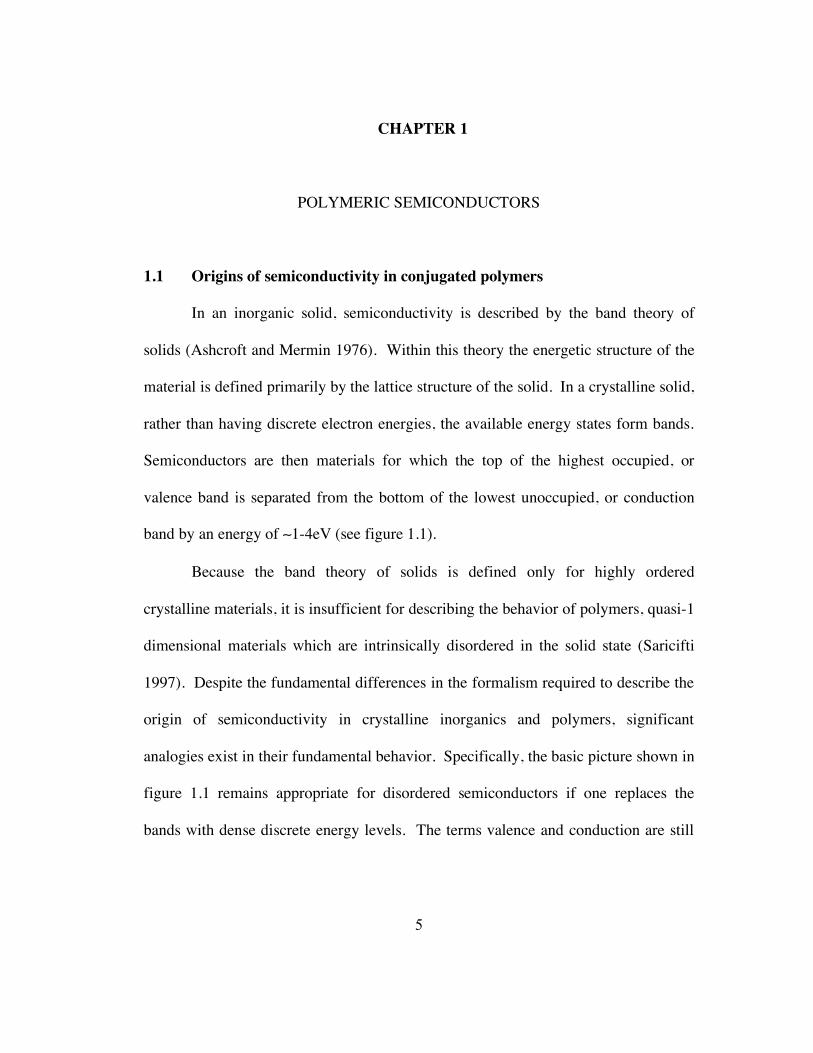
An illustration of the orbitals of polyacetylene is shown in figure 1.2. In
reality, the p hybrid orbitals form %-molecular orbitals that are delocalized along the
polymer backbone and provide a conductive pathway along the chain (Roth 1995).
Using methods of molecular orbital theory we are able to draw the energy levels of
electrons in these materials as they arise from the combination of individual atomic
levels (figure 1.3). In general the energy gap is ultimately defined by the energy level
splitting between the bonding and antibonding orbitals created between neighboring
carbon pz orbitals. Because they are necessarily off-axis, they are then % and %* levels
(Kagan 1993). The terms HOMO (highest occupied molecular orbital) and LUMO
(lowest unoccupied molecular orbital) are introduced here and become analogous to
the top of the valence band and the bottom of the conduction band, respectively.
Another factor that influences the energy levels of electrons in a polymer and
thus the ultimate bandgap energy is the conjugation length. The conjugation length
refers to the distance along the polymer chain with uninterrupted delocalization of
molecular orbitals. The levels of the delocalized segments are adjusted due to
quantum mechanical particle-in-a-box type effects, in which energy levels are
inversely proportional to the square of the conjugation length. In general, then, a
shorter conjugation length will result in a larger bandgap and blueshifted absorption
and emission.
9
Figure 1.3 Energy level splitting of orbitals in a conjugated polymer according to
molecular orbital theory.
1.2 Absorption and emission processes
The presence of an energy gap of between 1 eV and 4 eV allows for the
absorption and emission of photons in the visible wavelength range. The potential
energy curves as a function of internuclear distance for a diatomic molecule are
shown in figure 1.4, and are assumed to be a good approximation to the
chromophores in a conjugated polymer (Rohatgi-Mukherjee 1978). At room

10
temperature, electrons can be found in the lowest vibrational levels of the ground
electronic state. In general, therefore, an absorbed photon with an energy greater than
the bandgap excites an electron from the lowest vibrational level in the ground
electronic state to a vibrational level in the excited electronic state. The excited
electron quickly undergoes vibrational transitions until it reaches the lowest level of
the excited electronic state. Typically the timescale of a vibrational transition is much
faster than that of fluorescence or phosphorescence and therefore the relaxation of an
excited electron to the ground electronic state always occurs from the lowest
vibrational level of the excited electronic state.
Upon examination of the features of figure 1.4 one can see that the absorption
of the material will be blue-shifted from the emission for any material with a non-zero
horizontal separation between the excited and ground state potential minima. The
band shapes also determine to some extent the spectral overlap between the
absorption and emission spectra. The wavelength separation between the peak of
absorption and emission of a material is known as its Stokes shift. An example is
shown in figure 1.5. The Stokes shift and spectral overlap are important in
determining the energy loss through heating of an excited electron upon emission as
well as the probability of an emitted photon to be reabsorbed, in a sense dictating the
usefulness of a material for various applications. In most cases, a small Stokes shift
with little spectral overlap is desired.

11
Figure 1.4 Potential energy as a function of internuclear distance for the ground
and first excited states of a diatomic molecule. Absorption occurs from the lowest
vibronic level of the ground state and emission occurs from the lowest vibronic level
of the excited state.

12
Figure 1.5 Example absorption and emission spectra, Stokes shift, and spectral
overlap.
Excited carriers can be generated through photoexcitation or through the
injection of an electron and a hole into the LUMO and HOMO, respectively (Kagan
1993). These processes are depicted in figure 1.6. Upon photoexcitation, an electron
is promoted from a ground state singlet to what is known as a singlet exciton.
Because fluorescence is a singlet-singlet transition, the theoretical maximum internal
quantum efficiency for photoluminescence is 100%. With injected carriers, however,
the injected electron and hole can form either a singlet or triplet state. Assuming an
equal probability of each reduces the maximum internal quantum efficiency for
electroluminescence to 25% (Helfrich and Schneider 1966). Recently, however,

13
studies have suggested that the long assumed maximum efficiency of 25% may not
hold, although the subject is a matter of intense debate (Reufer et. al. 2005).
Figure 1.6 Exciton formation from a) photoexcitation and b) injected carriers.
The various pathways for recombination of a singlet exciton are shown in
figure 1.7. The excited exciton can decay non-radiatively (in the form of heat) or
radiatively (fluorescence) directly to the ground state. Alternatively, the exciton can
undergo a singlet-triplet intersystem crossing. The energy of the triplet states are
below that of the excited state, therefore a triplet exciton must undergo a non-
radiative or radiative (phosphorescence) triplet-singlet intersystem crossing to return
to the ground state (Kagan 1993).

14
Figure 1.7 Pathways for recombination of a singlet exciton in a conjugated
polymer.
The nature of the excited carriers themselves have been a subject of debate in
recent years (Jenekhe and Osaheni 1994). It is generally accepted that the primary
excitation in conjugated polymers is the singlet exciton. The singlet exciton consists
of an electron in the LUMO and a hole in the HOMO bound by Coulomb attraction.
The binding energy of a singlet exciton is typically 0.1eV- 0.5eV and accounts for the
difference between the ‘electrochemical bandgap’ (defined by the low energy onset of
absorption) and the ‘optical bandgap’, defined by the absorption maximum.
Evidence suggests, however, that the singlet excitons alone can not account
fully for the observed properties of the excitations in conjugated polymer films.
Because the polymer chains in thin film are randomly distributed and amorphous
(figure 1.8), the possibility exists for the delocalized %-orbitals in one conjugation

15
segment of the polymer to overlap with another conjugation segment on the same
chain or on a neighboring chain. Such excitations are referred to as excimers,
exciplexes, and aggregate states, and generally result in a broad red-shifted feature in
the polymer emission (Jenekhe and Osaheni 1994).
Figure 1.8 Amorphous polymer in thin film form.
1.3 Doping of semiconducting polymers
Much of the earlier work done attempting to understand the fundamental
effects of chemical or electrochemical doping in semiconducting polymers has
focused on exploring structural differences in doped and non-doped
poly(phenylenevinylene) (PPV). Bradley et. al. 1987 did a study of the infrared and
optical absorption spectra for both non-doped and electrochemically p-doped PPV.
Their results showed that electrochemically p-doped PPV demonstrated additional
energy levels within the bandgap as evidenced by the appearance of new peaks in the

16
optical absorption spectra of the doped sample. They suggested that the energy levels
were consistent with the formation of bipolaron defects in the doped polymer film. In
addition they showed that p-doping created additional peaks in the IR absorption
spectra that appeared to be independent of dopant type. Lefrant et. al. 1989 then
presented a complementary study which looked at the IR and Raman scattering from
non-doped and chemically doped PPV. Modeling of experimental results suggested
that the polymer is structurally modified along the backbone by these polaron defects
from a benzoid to a quinoid form as a direct result of doping (figure 1.9).
Figure 1.9 Molecular structure of the PPV repeat unit in (a) benzoid (non-doped)
and (b) quinoid (doped) form.
Both theoretical and experimental work has since been extended to more
thoroughly understand the structural changes of doping in PPV and the resulting
change in the properties of the material but the general picture has not changed. Tian
et. al. 1991 used the theory of the effective conjugation coordinate (ECC) to further
support the concept of a doping-induced quinoid structure in PPV, Orion et. al. 1998

17
looked at chemically n-doped PPV and found that the fundamental changes in
structure are essentially the same as seen in the p-doped material, and Tzolov et. al.
2000 presented similar results using photothermal deflection spectroscopy. The
general understanding of the fundamental effects of doping in PPV is that doping
does not significantly alter the original energy levels of the material but instead
inserts levels within the bandgap through structural modifications (figure 1.10).
Doping does not simply add charges to the conduction band or take them away from
the valence band. This is because the strong coupling between the electrons and
phonons characterizing the polaron and bipolaron tends to cause distortions in the
polymer backbone. Furthermore this effect does not appear to be dependent on
dopant type or whether the polymer was doped chemically or electrochemically.
Another consequence of the existence of polarons or bipolarons in the doped
polymer material is that as the doping level is increased, the additional mid-gap
energy levels begin to form a polaron band, partially filled and thus electrically
conducting (Epstein 1997). However, because of the disordered nature of the
polymer materials, the charge carriers tend to be highly spatially localized. Therefore
charge transport occurs primarily through hopping (Monroe 1985). Arkhipov et. al.
2003 have shown that the dependence of charge carrier mobility on charge carrier
density is dominated by the generation of a random Coulomb field by dopant ions
which broadens the DOS distribution and decreases mobilities for low dopant
concentrations, and by the filling of deep traps which facilitates hopping and
increases mobilities at higher dopant concentrations.

18
Figure 1.10 Energy levels of a conjugated polymer in (a) neutral form, with
conduction and valence bands only, (b) lightly doped, with the addition of a single
bipolaron energy level, and (c) more heavily doped, with a broad bipolaron band.
Despite the unanimous assignment of doping-induced structural changes in
conjugated polymers to polaronic-type defects, considerable disagreement exists
about whether these defects in the polymer film appear as polarons, bipolarons, or
both depending on conditions. A simple depiction of the formation of polarons and
bipolarons is shown in figure 1.11. An intermediate state, loosely termed the ‘nuetral
polaron’, is formed in which an electron is shifted to a dangling p orbital, leaving a
radical cation and forcing a rearrangement of carbon bonds from the previously
mentioned benzoid to quinoid form. Because a single defect introduces an
energetically unfavorable domain wall, the system prefers to form two.
If an electron is added (reduction) or removed (oxidation) to one of the
dangling p orbitals the resulting defect is termed a negative or positive polaron. If
this occurs at both defect sites, this is termed a bipolaron. The primary difference

19
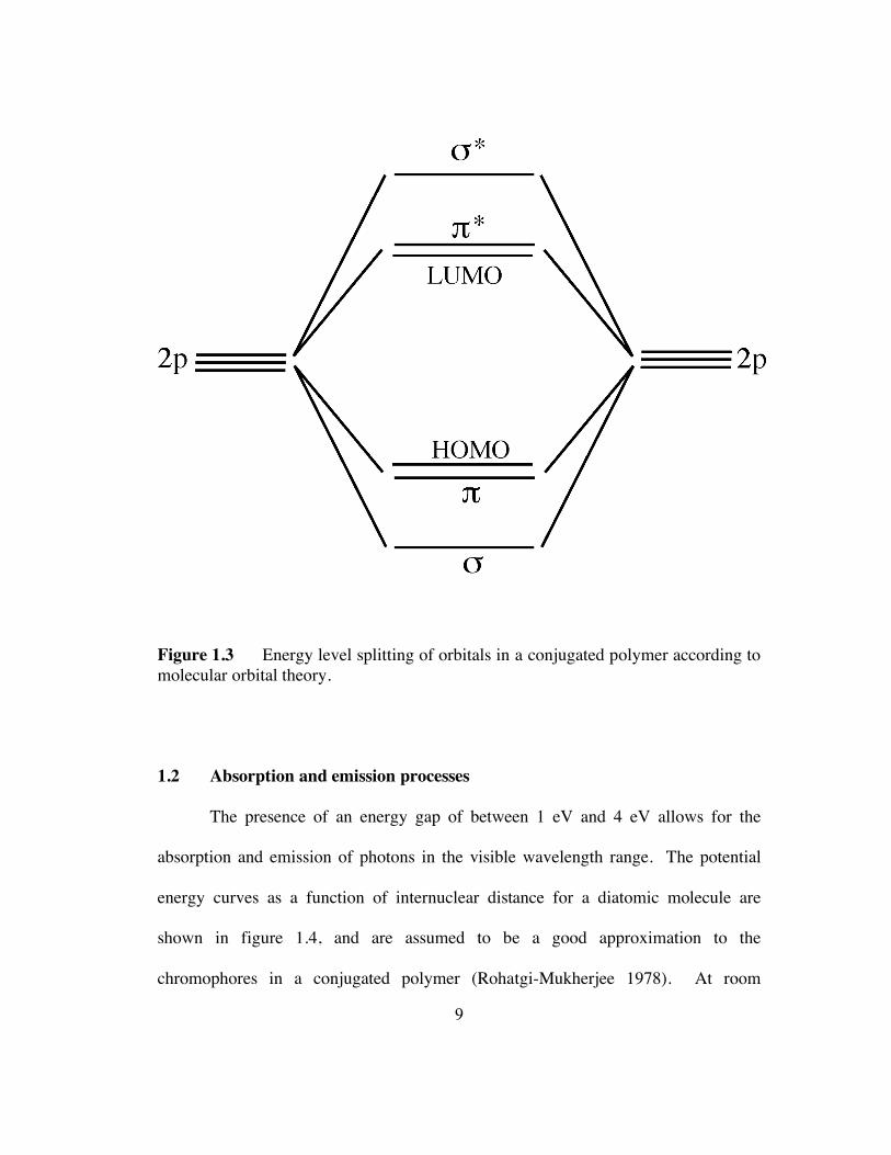
between the polaron and bipolaron is in the allowed electronic transitions. The
energetic structure and allowed transitions for polarons and bipolarons are shown in
figure 1.12.
Figure 1.11 The formation of polaron and bipolaron defects in a conjugated
polymer.
20
Figure 1.12 Energetic structure of a material with polaron and bipolaron defects
and allowed electronic transitions
The most favorable defect with doping and its depiction in ESR, Raman and
absorption data is currently in debate. Theoretically, models using the Su-Schrieffer-
Heeger model Hamiltonian (Su et. al. 1980, Shimoi and Abe 1994), find bipolarons to
be more energetically favorable due to the greater lattice relaxation while others
(Bredas et. al. 1984), which consider electron-electron interactions, find that because
of Coulomb interactions, polarons are energetically more stable until high doping
levels are reached where bipolarons are formed. Many initial experimental
investigations concluded that polarons were present in lightly doped systems followed
by bipolaron formation with greater doping confirmed by observed optical transitions
and ESR studies (Bredas et. al. 1984, Patil et. al. 1997). The intensities of the optical
transitions though did not agree with the intensity relationships proposed by the FBC
model.

21
More recently, Furukawa reassigned observed transitions to remedy the
intensity anomaly argued that polarons are the primary doping species in non-
degenerate polymers and the ESR results are due to polaron-polaron interactions
(Furukawa 1996). However, the energy transition reassignments do not add up to the
interband transition. Others using vibrational spectroscopy have come to the
conclusion that polarons and bipolarons are both present in thermal equilibrium at
high doping levels (Baitoul et. al. 1997, Baitoul et. al. 2000). Still others suggest that
two transitions correspond to polarons and one transition corresponds to bipolarons
and that previous doping levels were not high enough to detect the single transitions
associated with bipolarons (Apperloo et. al. 1999).
While much of the fundamental research on doping in light-emitting polymers
has focused on PPV, studies have also been done on the electrochemistry of some of
the PPV derivatives, mainly in an effort to understand how the addition of various
sidechains affects the properties of the material. Eckhardt et. al. 1989 studied a
variety of PPV and poly(thienylene vinylene) derivatives, comparing the non-doped
optical absorption spectra and using electrochemical measurements to compare the
bandgap in each material. In a similar study, Li et. al. 1999 compared 10 PPV
derivatives, focusing on the doping potentials for thin films as well as in an LEC
configuration. They concluded that the presence of electron donating sidegroups
tends to lower p-doping potentials, while electron accepting sidegroups tend to make
the p-doping and n-doping potentials more electronegative.

22
CHAPTER 2
OPTOELECTRONIC POLYMER DEVICES
2.1 Light-emitting diodes
The first inorganic LED’s came into commercial production in the 1960’s.
Slowly, technology improved to include a wider variety of colors and higher
efficiencies, but it wasn’t until 1990 that the ability to create a diode using conjugated
polymer was reported (Burroughes et. al. 1990). In 1991, Braun and Heeger reported
light emission from PLED’s made with the soluble semiconducting polymer MEH-
PPV (Braun and Heeger 1991). Since then, the field of PLED’s has grown
tremendously with the development of a wide range of colors and the appearance of
some of the first commercially viable polymer based displays.
The state-of-the-art LED is based on doped crystalline semiconductors. A
basic sketch of a p-type and n-type semiconductor and its corresponding energy
diagram is shown in figure 2.1 a) and b), respectively. In p-type doping, a molecule
from the lattice is replaced by an acceptor molecule; that is, one that requires an
additional electron to complete a bond. Acceptors introduce an energy level close to
the semiconductor’s valence band. At room temperature, electrons in the valence
band have enough energy to move into the new energy level, allowing for the
movement of a free hole through the material. Similarly, in n-type doping, a donor

23
molecule is introduced that adds an energy level close to that of the semiconductor’s
conduction band, and a free electron is introduced to the material.
Figure 2.1 Lattice structure and energy band diagram for (a) p-type and (b) n-type
crystalline semiconductor.
A p-n junction is formed by making contact between a p-type and an n-type
semiconductor. This process is illustrated in figure 2.2. Prior to the junction
formation, we have a neutral piece of p-type and n-type semiconductor, with energy
bands and Fermi levels as shown in figure 2.2(a). After contact is made, the free
electrons at the n side of the junction fall into the free holes on the p side, leaving a
region on the p side of the junction with a net negative charge and vice versa for the p

24
side. This sets up a region known as the depletion zone with a non-zero electric field
and no free charge carriers. Upon junction formation, the Fermi levels of the two
sides match up and the conduction and valence bands on either side of the junction
bend in response to the built-in electric field. Clearly after the junction has been
established, it becomes energetically unfavorable for free charge carriers to wander
into the depletion zone in the absence of an external electric field. By forward-
biasing this system, charge injection is initiated. A typical LED is then a forward-
biased p-n junction constructed using suitably chosen materials.
Figure 2.2 Formation of a p-n junction.

25
The mechanism governing the operation of a polymer LED (PLED) is quite
different from that of a crystalline semiconductor based LED. The origin of the
semiconducting nature of these polymers itself, as described in section 1b, must be
described using molecular orbital theory rather than semiconductor band theory, in
contrast with the materials described above. In addition, the optimal configuration for
a PLED could be described as a metal-insulator-metal diode (MIM), with the central
layer being the non-doped semiconducting polymer, instead of the previously
described p-n junction configuration.
The PLED’s described in this work are constructed using a sandwich structure
as shown in figure 2.3. Using the experimental methods described in section 4a, a
layer of PEDOT-PSS (Bayer corp.) is spin cast onto an ITO patterned glass substrate
(Thin Film Devices Inc.) to function as the device’s anode. The polymer layer is then
spin cast above, and finally a layer of calcium followed by aluminum is thermally
evaporated to serve as the cathode. The function of the PEDOT-PSS is twofold; it
assists in hole injection into the device and creates a smooth even surface on which to
spin the polymer film. The calcium functions as the effective cathode of the device;
an evaporated layer of aluminum is added to the process to help barrier the calcium
against oxidation. A typical energy level/ work function diagram for such a device is
given in figure 2.4.

26
Figure 2.3 Polymer LED device structure with Ca/Al cathode and PEDOT-
PSS/ITO anode.
Figure 2.4 An example energy level/ work function diagram for a PLED. The
HOMO/LUMO levels for the polymer shown are that of MEH-PPV (Campbell et. al.
1996, Bozano et. al. 1999). In this example, no barrier exists for electron injection.

27
A schematic diagram of this type of device structure in forward bias is
illustrated in figure 2.5. Electrons from the cathode are injected into the LUMO of
the polymer on one end of the device, and holes are injected from the anode into the
polymer HOMO on the other. The charge carriers recombine within the polymer
layer and emit light. Therefore, the three main processes affecting the operation of
the device are charge injection, charge transport, and recombination.
Figure 2.5 Schematic diagram of a PLED in forward bias illustrating the charge
injection, transport, and recombination processes.

28
Charge injection is characterized primarily by the difference between the
electrode work function and the polymer HOMO/LUMO levels. The two primary
mechanisms for charge injection into a polymer diode with an energetic barrier to
charge injection are referred to as Fowler-Nordheim tunneling (Fowler and Nordheim
1928) and thermionic injection, shown schematically in figure 2.6 a) and b),
respectively. Both types of charge injection reduce to Ohmic behavior in the limit of
zero barrier height, the condition which provides optimal charge injection. Parker
proposed a model for the behavior of a polymer LED that is dominated by Fowler-
Nordheim tunneling (Parker 1994). However, Davids showed that for low barrier
height, thermionic emission actually dominates over F-N tunneling (Davids et. al.
1997).
Figure 2.6 Two proposed methods for charge injection in a PLED include a)
Fowler-Nordheim tunneling and b) thermionic injection.

29
While injection plays a major role in the operation of a PLED, in many cases
it is charge transport that dominates the device characteristics. For large energy
barriers the device is injection limited, while for lower energy barriers, the current is
space-charge limited (Davids et. al. 1997). Blom found that in PPV-based PLED’s,
the hole-current tends to be space-charge limited while the electron-current tends to
be trap limited (Blom et. al. 1997). Malliaras and Scott show that the recombination
profile depends heavily on the ratio of electron and hole mobilities and less so on
choice of contacts (Malliaras and Scott 1998).
The mechanism for charge recombination in PLED’s has been shown to
follow the theoretical Langevin process (Blom and de Jong 1998). In this model, the
charges undergo a random walk, and those that come within Coulomb’s radius of
each other will recombine (Langevin 1903), where the Coulomb radius is defined as
the distance at which the thermal energy equals the electron-hole binding energy.
2.2 Light-emitting electrochemical cells
The light-emitting electrochemical cell (LEC) first appeared in the literature in
1995 (Pei et. al. 1995). This device type is similar in construction to the polymer
light-emitting diode, but operates using a very different mechanism. The emitting
layer in an LEC incorporates a salt and a solid electrolyte into the light-emitting
polymer layer. The exact role of the ions in the operation of the LEC is under some
debate (see below). The primary practical differences between the two are that the

30
LEC is operationally independent of the electrode work functions, which allows
moving away from the highly reactive cathode materials commonly used in PLED
fabrication, and that it has the ability to emit light in both forward and reverse bias.
Because of these promising features, the LEC has been pursued extensively for
application. However much of the physics involved in the operation of this device
type has yet to be fully explored.
The LEC’s described in this work are constructed using a relatively simple
device design as shown in figure 2.1. The LEC ink is a mixture of light emitting
polymer, a polymeric ion transporter (solid electrolyte) such as polyethylene oxide
(PEO), and a salt, such as Li or Ca triflate or tetrabutylammonium tetrafluoroborate.
The ink is spin cast on the ITO glass substrate and a cathode, typically Al, is
thermally evaporated on top, following the experimental methods described in section
3.2. The PEO forms a network after thermal annealing that assists in the conduction
of ions through the polymer film.
Figure 2.7 A typical LEC device structure.

31
The initial report on the operation of LEC’s, as well as much of the
subsequent follow-up research, was published by Alan Heeger’s group at UNIAX
Corp. (Pei et. al. 1995, Yang and Pei 1996, Pei et. al. 1996). According to this group,
the LEC operates as follows: The salt dissociates to form free ions within the
polymer film. Under the applied electric field, the ions move, assisted by the
admixed electrolyte, toward the electrodes (see figure 2.2.). The ions then
electrochemically dope the polymer under the applied electric field, p-type near the
anode and n-type near the cathode, to form a p-n type junction in the bulk of the
emitting layer (Pei et. al. 1995). Because the doped polymer film is conductive (see
section 1.e.), contact between the film and the electrode becomes Ohmic, and
therefore charge injection no longer depends on the work function of the electrodes as
it does for the PLED. In addition, due to the reversibility of doping in conjugated
polymers, the junction formed is reversible and light emission becomes possible
under reverse bias.

32
Figure 2.8 Proposed operating mechanism for an LEC. Under external bias, the
ions move to opposite sides of the device. With a high enough voltage, the ions
electrochemically dope the polymer to form a p-n type junction within the device.
Following this initial publication describing the operating mechanism of an
LEC, attempts were made to further explore these devices by theoretically modeling
their I-V characteristics (Smith 1997, Riess and Cahen 1997). While Riess and
Cahen were able to model an LEC using the assumption of the formation of a pn-
junction in an LEC, Smith showed that the nature of the junction formed in an LEC is
quite different in nature than a standard pn-junction. Both models assume p-type
doping near the device anode and n-type doping near the device cathode.
In 1998, however, an alternate operating mechanism was proposed by R.
Friend’s group (deMello et. al. 1998). According to this group, the ions play the
central role in the operation of an LEC, but no doping takes place. Instead, the ions
that accumulate near the electrodes create a region with high ionic space charge,

33
resulting in a large electric field at the polymer-electrode interface that reduced the
barrier to charge injection (deMello et. al. 1998). This results in a very low electric
field in the bulk of the polymer, with charge movement within the film being
dominated by diffusion (figure 2.3). This proposed theory is also capable of
explaining the observed behavior of LEC’s (Ohmic contacts and reversible light
emission).
Figure 2.9 Alternate proposed mechanism for LEC operation. Ion accumulation
creates a large electric field at the electrode-polymer interface, reducing the barrier to
charge injection. Charge movement through the low electric field in the bulk of the
film occurs primarily through diffusion.
Although the disagreement over the fundamental operating mechanism of the
LEC has not been satisfactorily resolved, the progress toward improving the LEC and
better understanding its basic characteristics has not been hindered. Early on, it was
34
demonstrated that the addition of a surfactant-like additive (octylcyanoacetate)
improved the polymer/electrolyte network and therefore the operation of an LEC
(Cao et. al. 1996), and two-color emission was achieved by forward- or reverse-
biasing a bilayer LEC (Yang and Pei 1996). More recently, mutilayered
polymer/electrolyte devices were reported to improve the LEC (Lee et. al. 2002), and
a change in EL spectrum in forward- vs. reverse- bias was reported, giving clues to
the location of light emission in an LEC.
2.3 Electrochromic devices
Electrochromism is defined as an electrochemically induced color change. In
particular, it is the change in optical absorption bands brought on by an
electrochemical redox reaction in a material. A discussion of electrochromism first
appeared in the literature in the early 1960’s (Platt 1961). Since then
electrochromism has been demonstrated in a variety of materials, both inorganic and
organic, and has been utilized to develop contrast-based display and various other
technologies (Monk 1995).
A solid-state device that changes color upon application of an external bias is
called an electrochromic device (ECD). Such devices can be assembled into a
display. Electrochromic displays are passive; that is, they require external lighting to
view. Therefore the primary competing technology is liquid crystal displays

35
(LCD’s). The advantages of ECD’s for display application are the persistent image
with little or no additional power input, the ability to make large area displays, and
the ability to use polyelectrochromic materials for multiple colors per pixel.
Currently commercial applications for ECD’s include darkening rear-view mirrors
(Baucke 1987) and limited display applications.
Several organic materials have been established as displaying promising
electrochromic behavior. In particular, bipyridilium has been pursued extensively.
Several organic polymer systems display well-known electrochromic behavior
including polyaniline (Kobayashi et. al. 1984), polypyrrole and polythiophene
(Garnier et. al. 1983). Currently, there is limited understanding of electrochromism in
light-emitting conjugated polymers. An exception is a study on the electrochromic
behavior of MEH-PPV by Santos et. al. that demonstrates a near-reversible color
change upon electrochemical oxidation (Santos et. al. 2002).
The electrochromic devices presented in this work are constructed using the
sandwich structure illustrated in figure 2.1. A polymer layer is spin-cast on one piece
of ITO glass and a gel electrolyte layer is spin-cast on another, as described in section
4a. The two are then pressed together and dried overnight. The use of a second ITO
glass electrode rather than an evaporated metal electrode facilitates transmission
measurements. In this device structure the top ITO layer is commonly referred to as
the working electrode because it is the electrode at which the redox reaction takes
place, and the lower ITO layer is referred to as the counter electrode because it is the

36
electrode that completes the circuit, following the conventions established in two-
electrode electrochemistry experiments. The device is operated with the working
electrode biased as the anode and the counter electrode as the cathode. Upon
application of the external voltage, the anions in the electrolyte diffuse into the
polymer layer and oxidize it near the working electrode.
Figure 2.10 A typical ECD device structure.
The analysis of an ECD typically consists of measuring the change in the
absorption of the polymer layer in the non-doped and the doped state. Properties of
interest of an ECD determined in this way include !%T, or the change in percent
transmission, and the write-erase efficiency, expressed as a ratio absorbance changes
of the non-doped state after repeated cycles. Measuring the current and time of
voltage application also allows the characterization of the response time and the

37
coloration efficiency, measured as the change in absorption coefficient divided by the
charge transferred per unit area.
2.4 Interference in multilayered device structures
Two distinct types of interference effects are present in a typical polymer
light-emitting device structure with one highly reflective cathode (such as gold or
aluminum) and an ITO anode (a highly transparent but slightly reflective metal). The
first is wide-angle interference (Fig. 2.11.a) in which light emitted from within the
device toward the rear electrode reflects off of the reflective cathode and interferes
with the light directly emitted toward the viewing side. Wide-angle interference
tends to pick out wavelengths
!
" = 4nl, where n is an integer and
!
l is the distance
from the location of light emission to the reflective cathode.
The second type of interference present in such structures is multiple-beam
interference (Fig. 2.11.b). In this type of interference light emitted within the device
reflects between the ITO and reflective top electrode multiple times, resulting in the
selection of wavelengths correlating with the resonant mode of the cavity. In general
for device thickness less than half the wavelength of light the multiple-beam
interference results in a blue-shift. Because the reflectivity of the ITO is generally
low, wide-angle interference tends to be the dominant process in polymer light-
emitting devices.

38
Figure 2.11 (a) Wide-angle and (b) multiple-beam interference effects in polymer
light-emitting devices.
Because organic light-emitting devices consist of multiple layers with varying
refractive indices and typically one highly reflective electrode, optical interference
effects can be critically important in determining the spectrum and intensity of
emitted light (Leger et. al. 2003). The parameters that are necessary for the
simulation of interference effects in multilayered devices include the thickness and
wavelength-dependent complex refractive indices of each layer, the
photoluminescence spectra of the polymer material, and the location and profile of
light emission within the active layer.
In the absence of a light source, one can write the solution to the one-
dimensional Helmholtz equation
!
d2"dz
2 + k2
" = 0 as the superposition of a right and
left traveling plane wave
!
" ="+eikz
+"#e#ikz
. In layered media, the continuity
conditions at layer boundaries can be written in matrix form (Lekner 1987, Bjork et.
al. 1991). For instance, the boundary transfer matrix relating the amplitudes
!
"+ and
!
"# of the adjacent layers l and l+1 for S-polarization reads

39
!
"l
+
"l
#
$
% & &
'
( ) ) =1
2
1+kl+1
kl
1#kl+1
kl
1#kl+1
kl
1+kl+1
kl
$
%
& & & & &
'
(
) ) ) ) )
"l+1
+
"l+1
#
$
% & &
'
( ) ) , (1)
where the wavenumber
!
k = 2"n /# depends on the wavelength
!
" and the refractive
index n, which becomes complex in the case of absorptive media. In addition, the
propagation transfer matrix for plane wave propagation in a layer of thickness
!
"z
reads
!
" l
+
" l
#
$
% & &
'
( ) ) =
exp jk*z( ) 0
0 exp # jk*z( )
$
% & &
'
( ) ) " l+1
+
" l+1#
$
% & &
'
( ) ) . (2)
Thus, by multiplication of layer and boundary transfer matrices from multiple layers
an effective matrix relating the wave amplitudes at different locations in the
multilayer structure is obtained, from which the reflection and transmission Fresnel
coefficients r and t are derived.
For the simulation of light emission in a layered medium the inhomogeneous
Helmholtz equation with a source consisting of an oscillating point dipole needs to be
solved (Crawford 1988, Lukosz 1981, Neyts 1998). Dipole methods have previously
been used successfully to model organic LED emission (Burns et. al. 1996, Kim et.
al. 2000). Such simulations in general require the distinction of parallel and vertical
dipole orientations as well as S and P-polarization. However, for emission in the
normal direction the expression for the emitted power density simplifies to
!
P~
!
1+ rl
" exp 2iklz"( )
2
1" rl
"rl
+exp 2ik
ldl
( )2 # tl
+ 2
, (3)

40
(Neyts et. al. 1998) where
!
rl
+,
!
rl
", and
!
tl
+ are the Fresnel coefficients for light
originating in layer n, and
!
z" is the distance of the dipole from the lower boundary of
layer n whose thickness is
!
dl. In expression (3) the denominator accounts for layer
thickness dependent multiple beam interference while the nominator depends on the
dipole position within this layer.

41
CHAPTER 3
EXPERIMENTAL TECHNIQUES
3.1 Cyclic voltammetry
The experimental technique known as cyclic voltammetry (CV) is a versatile
tool which allows the electrochemical characterization of a wide variety of materials.
The fundamental process of doping in semiconducting polymers can be most directly
explored using this technique. Cyclic voltammetry primarily provides information
about the onset voltage and reversibility of doping in a material. In addition, the
experimental setup can be used to generate doped samples for additional study. A
main component of this research involves using cyclic voltammetry data for a study
of light-emitting polymer materials, allowing a study of the electrochemical doping of
MEH-PPV (chapter 6) as well as the temperature dependence of the HOMO/LUMO
levels of two related materials (chapter 8).
The core of the experimental setup used in cyclic voltammetry is the typical 3-
electrode electrochemical cell pictured in figure 3.1. The components of this setup
include a working electrode, an auxiliary, or counter, electrode, and a reference
electrode all submerged in electrolyte solution. The working electrode is the
electrode at which the electrochemical redox reaction takes place. The reference
electrode is used to measure the potential at the working electrode, and is typically

42
one whose electrochemical potential is well known and constant in the absence of
current flow. The auxiliary electrode is an inert conductor which completes the
circuit. In cyclic voltammetry, the potential between the working and reference
electrodes is cycled between fixed values. Ions from the electrolyte solution dope the
sample at the working electrode, creating a cell current through the circuit. This
current is measured and provides information about the doping of the sample.
Figure 3.1 Typical 3-electrode electrochemical cell (with film sample) used in cyclic voltammetry experiments.
In the experiments described in this work, the working electrode consists of
polymer spin-coated onto an indium tin oxide (ITO) coated glass substrate. The ITO
substrate is highly conductive and largely transparent, allowing for the subsequent
study of the optical properties of the polymer films, such as the optical absorption and

43
photoluminescence spectra. Electrical contact is established with a platinum wire
secured to the ITO substrate just above the polymer film. The auxiliary electrode is a
simple platinum wire. Our reference electrode is 3 M Ag/AgCl with a reference
voltage of !.207 V. The typical electrolyte solution used is .01 M
tetrabutylammonium tetrafluoroborate (TBABF4) in acetonitrile (AN). A nitrogen
inlet is included, and the entire cell is flushed with nitrogen gas prior to running the
experiment, as the setup is sensitive to the presence of air in the cell.
The potential between the working and the reference electrode is controlled
with the use of a potentiostat. In cyclic voltammetry, the potentiostat cycles the cell
potential linearly using a triangular waveform (figure 3.2). The circuit is completed
between the working electrode and the auxiliary electrode to avoid current flow
through the reference electrode. Therefore the potential between the working
electrode and the reference electrode is measured and controlled using a feedback
loop (figure 3.3). The cell potential and cell current are then measured by the
potentiostat and read into the computer (figure 3.4). The potentiostat used in the
experiments reported in this work is an EG+G Model 362 scanning potentiostat. Two
Keithley multimeters, 2000 and 2010, are used to measure the voltage and current
from the potentiostat. A Labview script was constructed to measure the output of the
multimeters into data files.

44
Figure 3.2 Triangular waveform generated by the potentiostat in a typical cyclic voltammetry experiment.
Figure 3.3 Basic potentiostat layout.

45
Figure 3.4 Experimental setup for cyclic voltammetry. Voltage and current are monitored with multimeters that are external to the potentiostat.
The current-voltage data taken in a cyclic voltammetry experiment is referred
to as a voltammogram. An example of a voltammogram for an ideal system is given
in figure 3.5. In the forward scan, we start the system at point A and start increasing
the voltage according to figure 3.2. The oxidation reaction begins shortly and peaks
at point B. Eventually the material becomes completely doped, and the current
through the circuit stabilizes. At point C, the voltage peaks and reverses. The doping
in the material begins to reverse, resulting in a negative current which peaks at point
D. Again this current subsides and stabilizes at point E.
The critical parameters of such a voltammogram are
!
E pc ,
!
E pa ,
!
Ipc , and
!
Ipa .
In this notation, p refers to the fact that we are in the forward, or oxidizing, scan (p-
doping). The cathodic values are then pc and the anodic values are pa. These values
give information about doping potentials and the reversibility of doping in a given
material. In an ideal, reversible system with a one-electrode reaction,
!
Ipc " Ipa , and

46
the peak separation
!
Epc " Epa = 58mV . The dependence on scan rate is seen in the
peak height, as
!
I" # , where " = scan rate, and
!
E pc and
!
E pa are independent of scan
rate. The increase in peak height as a function of scan rate can be understood by
considering that the number of reactions and therefore the total charge transferred
must be the same for all scan rates. While for faster scan rates the time step is
shorter, the integral of current as a function of time must remain constant and thus the
current is higher at the end of each step.
Figure 3.5 A voltammogram of an ideal system in forward scan.
For so-called quasi-reversible reactions, however, the peak separation will
always be larger than for the ideal case. Quasi-reversible behavior can be inherent to
the reaction studied in the case of slow reaction kinetics, or can arise from such
factors as limited ion mobility through the sample, contamination of the system by
oxygen or water, material loss, or a number of other factors. The peak position for a

47
quasi-reversible system increases as a function of scan rate, as the voltage step occurs
prior to the establishment of equilibrium in the sample. All reactions in this work
display quasi-reversible properties.
3.2 Device construction
All of the types of polymer devices described in chapter 2 have the same basic
architectures and methods of construction with the exception of the planar light-
emitting electrochemical cells, though the details of the polymer solutions and
cathode metals vary from one device type to another. In this section I describe the
broad details of device construction as they apply to all of the sandwich structure
devices studied in this work. The more detailed information about any particular
device will be given as the particular study is outlined. Some of the polymer
materials used in the study were obtained through academic collaborations and others
are commercially produced. The polymer materials are dissolved in various organic
solvents (typically chlorobenzene or toluene) and are stirred and often heated to
encourage the solids into solution.
The devices are made using glass substrates with patterned indium tin oxide
(ITO) as the transparent electrode (manufactured by Thin Film Devices, Inc.). The
ITO is deposited using RF sputtering, using a mask to achieve the desired pattern.
The substrate with ITO pattern is illustrated in figure 3.6. The ITO surface itself is

48
1500 Å thick with a surface roughness of !10 Å and a resistivity of 20 "/sq. The
substrates are cleaned with ethanol prior to use.
Figure 3.6 Device geometry at various stages of construction. a) ITO patterned substrate. b) substrate with polymer layer covering active device area. c) substrate with polymer layer and evaporated contacts.
The polymer layer(s) are formed by spin-casting the liquid polymer solution
on the ITO substrate. Spin casting involves placing the substrate on a vacuum stage
that holds the device in place as it spins rapidly (typically between 800-3500 rpm) for
30-40 seconds. The viscosity of the polymer solution and the spin speed determine
the final layer thickness and uniformity. Layer thickness is measured using an atomic
force microscope (see section 3.4). After the spin casting, the edges of the substrate
are wiped with solvent to expose the ITO contact pads (see figure 3.6). Often the
device is made with more than one polymer layer, as is the case for most LED’s
which include a layer of PEDOT-PSS (manufactured by Bayer Corp.) to even the ITO
surface and aid in hole transport (Carter et. al. 1997). In the case of a layered
structure, the first layer is spin cast on the substrate, and the solvent is then removed
from the layer before the next layer is spin cast on top. To ensure that the first layer

49
does not dissolve upon the addition of the second layer, the first material cannot be
soluble in the solvent of the second solution, which can prove to be a significant
limitation of layered structures.
In the work presented here, all device contacts are made using thermal
evaporation. The devices are placed in masks forming the contact geometry (shown
in figure 3.6) and placed in a vacuum chamber. A current is forced through a
tungsten boat containing the metal being used, which is then evaporated slowly
(approximately 1-3 Å/s) onto the device. The vacuum system used is an LH
Turbovac 150 turbo pump backed by an LH Trivac roughing pump and reaches
pressures ~10-6 torr. Contact evaporation is monitored using an LH Inficon
deposition monitor.
3.3 Measurement of photoluminescence and absorption spectra
The optical processes of absorption and photoluminescence discussed in
section 1.2 are of primary importance in that they essentially define the optical
properties of a given material. Measuring the absorption and photoluminescence
spectra of a material is a fairly straightforward experimental process. The absorption
and photoluminescence spectra of the specific materials used in this work are shown
in later chapters.
The absorption spectra for the various materials studied in this work were
obtained on various specific instruments as specified for each study. A brief

50
schematic for these instruments in transmission measurement mode is shown in figure
3.7. The absorption of a film of material is obtained by measuring the fraction of
light transmitted over the range of wavelengths of interest. The absorption is then
obtained using
!
A "( ) =1# T "( ) , where
!
T "( ) is percent transmission. To be precise,
this method ignores the fraction of reflected light
!
R "( ) . Typically, however,
!
R "( ) is
a small value for the materials used. In addition, the measurement of
!
R "( ) returns
both the reflected light as well as a significant contribution from photoluminescence,
thus lessening the accuracy of the measurement. We therefore approximate the
absorption spectra of our materials using the method described.
Figure 3.7 Brief schematic of the instrument used to measure the fraction of light transmitted through a film sample.
Films are made for absorption measurement by spin casting a polymer film
onto a transparent or nearly transparent substrate. Quartz substrates are used
whenever possible, however some studies reported in this work required the use of
ITO coated glass substrates for absorption measurements, in particular the samples
generated using cyclic voltammetry.

51
The photoluminescence data used in this work was taken on either a Perkin
Elmer LS 50B or LS 45 luminescence spectrophotometer. The material is
photoexcited at absorption maximum for an optimized signal. A schematic for these
instruments is shown in figure 3.8 with the instrument set up for (a) solution
measurement and (b) film measurement. To measure photoluminescence from
solution, we use dilute solution in a quartz cuvette. To measure photoluminescence
for a film sample, we typically spin cast the polymer film onto a quartz substrate.
Figure 3.8 Brief schematic of the instrument used to measure the photoluminescence of (a) dilute solution and (b) film sample. The film sample is mounted such that collection of reflected light in the photodetector is minimized.
3.4 Atomic force microscopy (AFM)
The experimental technique of Atomic Force Microscopy (AFM) allows for
the detailed (nm-scale) study of surface properties. In the field of polymer science,
applications can range from the study of film roughness and uniformity to the
measurement of a variety of local properties such as conductivity. In this work, AFM
is used primarily to determine polymer film thickness.

52
The operating mechanism of the AFM includes a sharp probe, or tip, that is
moved over the surface being studied (figure 3.9). This tip is mounted at the end of a
cantilever which moves up or down in response to the force between the tip and the
sample as it is moved across the sample in a raster scan. A laser is aimed at the tip
and detected by a split photodiode. In this way, as the tip moves in the vertical
direction in response to the surface profile, the difference in signal in the split
photodiode allows for the measurement of the height of the tip. In this work, the
mode used is referred to as contact mode, meaning simply that the tip remains in
contact with the surface in the repulsive regime of the intermolecular force.
Figure 3.9 The basic operating mechanism of the atomic force microscope (AFM).
The primary use for the AFM in this work is to determine the thickness of
various polymer films. To achieve this measurement, a small scratch is made in the

53
polymer film, and then imaged using the AFM. The profile of the scratch gives the
height difference between the film surface and the substrate, and the average is used
to obtain the thickness of the film (figure 3.10).
Figure 3.10 The profile of a polymer film during a thickness measurement.
3.5 Electronic characterization of devices
The electronic characterization of the devices studied in this project is
achieved primarily through the measurement of the device’s current-voltage
dependence (IV curves). This data gives important information about charge motion
through the device, including charge injection and charge mobility. When combined
with radiance measurements as described in section 3.6, the current-voltage
measurements can also be used to determine external quantum efficiency.

54
IV curves are taken with a Keithley 2400 sourcemeter in an inert nitrogen
atmosphere (glovebox). Data acquisition includes stepping through applied voltages
and measuring the current through the device. A LabView script controls this
procedure, allowing data acquisition to begin and end at any chosen voltage.
Variables include the size of voltage step and the delay between step and
measurement. A typical measurement delay for an LED is !500 ms. Because the ion
mobility is so much lower than electron or hole mobility in the polymer, the response
time of doping-dependent devices after a voltage step is much lower than for LED’s.
A delay for an LEC or ECD, therefore, is typically much longer, between 1000ms and
5000 ms depending on the device.
A typical IV curve for a polymer LED is shown in figure 3.11. At lower
voltages the device is dominated by diffusion current (see section 2.1). When the
applied voltage is equal to the turn-on voltage, charge injection is initiated and drift
current dominates. For many devices a slight kink can be seen in the IV curve at the
approximate turn-on voltage of that device. For an LED in forward bias with
properly chosen contact materials, the turn-on voltage is approximately equal to the
band gap of the polymer less the exciton binding energy. If the contact materials are
chosen such that the work functions of the contacts lie within the band gap of the
polymer, however, the turn-on voltage will be higher due to the extra energy required
to inject the charge carriers into the polymer. Analysis of the portion of the IV curve

55
that displays space-charge limited current yields information about charge mobility in
the polymer layer (see section 2.1).
Figure 3.11 Example IV curve for a polymer LED.
An IV curve for an LEC that emits light in both forward and reverse bias is
shown in figure 3.12. Despite the significant differences in the operating mechanism
of polymer LED’s and LEC’s, the IV curves of these device types display remarkably
similar features, with the exception of the reverse turn-on seen in the LEC. As
mentioned previously, however, the testing of an LEC requires a much longer step-
measurement delay due to the slow equilibration of the device, and frequently
significant hysteresis is evident upon repeated cycles of measurement.

56
Figure 3.12 Example IV curve for a polymer LEC.
An IV curve for a typical polymer ECD is shown in figure 3.13. An ECD is
essentially a solid state realization of a cyclic voltammetry experiment in the sense
that we are electrochemically doping a polymer film with either cations or anions by
cycling the system through a range of voltages in the presence of an electrolyte (see
section 2.3). Accordingly, the features of such an IV curve correlate quite well with
that of a cyclic voltammogram as described in section 3.1. ECD curves, however, do
not typically display the clean peaks and clear reversibility seen in the cyclic
voltammograms, due to the lowered ion mobility of the solid state.
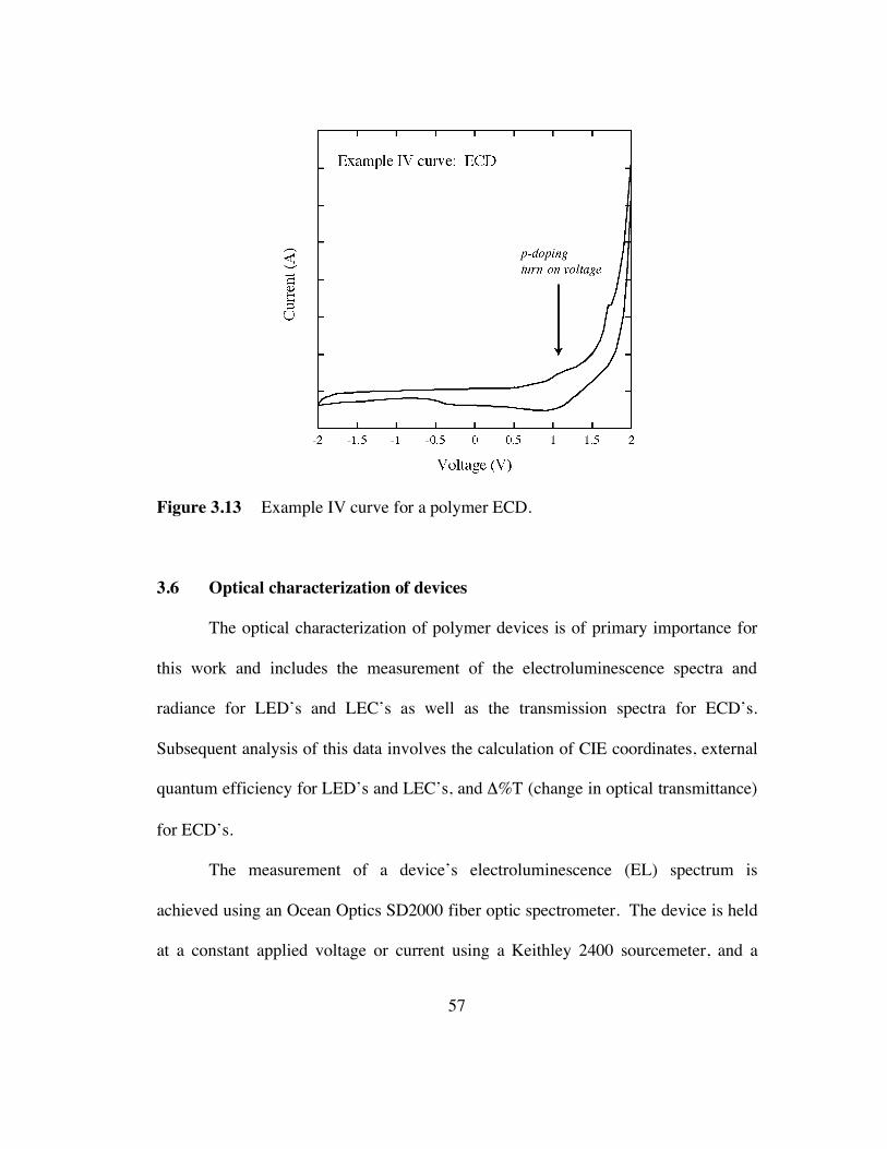
57
Figure 3.13 Example IV curve for a polymer ECD.
3.6 Optical characterization of devices
The optical characterization of polymer devices is of primary importance for
this work and includes the measurement of the electroluminescence spectra and
radiance for LED’s and LEC’s as well as the transmission spectra for ECD’s.
Subsequent analysis of this data involves the calculation of CIE coordinates, external
quantum efficiency for LED’s and LEC’s, and #%T (change in optical transmittance)
for ECD’s.
The measurement of a device’s electroluminescence (EL) spectrum is
achieved using an Ocean Optics SD2000 fiber optic spectrometer. The device is held
at a constant applied voltage or current using a Keithley 2400 sourcemeter, and a

58
LabView script is used to acquire spectral data in the form of photon counts as a
function of wavelength over a set period of time. From this information, the emitted
spectrum, average photon energy (eV), and radiant exitance (
!
W cm2 ) can be directly
obtained. By weighting the measured spectral power distribution with the response
function of the human eye, the values of luminous efficacy (lm/W) and luminous
exitance (
!
lm cm2 ) can be calculated. In addition, this distribution is used to calculate
the C.I.E. coordinates of the device (see below).
The measurement of the device radiance and external quantum efficiency is
done in tandem with the measurement of the current-voltage curve (see section 3.5).
The device is enclosed with pins allowing electrical contact to the device, and a Si
photodetector is placed on the ITO side of the device. The voltage is stepped linearly
as described in section 3.5. The light emission incident on the photodetector induces
a current through the photodetector that is read by a Keithley 485 picoammeter. This
data, in combination with the spectral information determined with the spectrometer,
gives the information necessary to determine the device luminance (
!
cd cm2 ) and
radiance (
!
W cm2 ).
The external quantum efficiency can also then be calculated using the
measured current through the device using the following definition;
External quantum efficiency =
!
# photons out
# electron - hole pairs in
This value is typically reported as the primary means of expressing the level of device
performance for a light-emitting device. An EQE plot for a polymer LED is shown in

59
figure 3.14. The quantum efficiency begins to rise at the turn-on voltage of the
device and eventually levels off. In theory the external quantum efficiency of a
device is the product of the internal quantum efficiency with factors such as the
amount of light emitted in the forward direction due to the geometry of the device and
the decrease in light intensity due to interference effects (see section 1.3).
Figure 3.14 A representative plot of external quantum efficiency as a function of applied voltage for a polymer LED.
The optical characterization of electrochromic devices involves mainly the
measurement of the change of the device’s transmission spectrum from the initial
(non-doped) state to the colored (doped) state. The measurement of a transmission
spectrum is described in detail in section 3.3. Typically the transmission spectrum is
taken for the non-doped state of the device, a voltage is applied to the device for a
given period of time, and then the transmission spectrum is quickly taken again for

60
the colored state before any bleaching can occur. The change in transmission spectra
is often reported as #%T for the wavelength within the visible that displays the
maximum difference in transmission. Finally, the transmission spectra are used to
determine the C.I.E. coordinates of the device as described below.
The C.I.E. chromaticity coordinates are used to map the color of an object
with respect to hue and saturation onto a two-dimensional C.I.E. chromaticity
diagram (figure 3.15). They are derived from either the electroluminescence
spectrum for a light-emitting object or the transmission spectrum for an
electrochromic device. The procedure for calculating the C.I.E. coordinates is as
follows: The spectrum used is first weighted by each of three C.I.E. color-matching
functions (figure 3.16). Each data column is summed to obtain the three C.I.E.
tristimulus values X, Y, and Z. The values are then normalized to obtain the C.I.E.
chromaticity coordinates x=X/(X+Y+Z) and y=Y/(X+Y+Z). This is the most
common procedure for reporting color despite the limitations of the C.I.E. color
system such as the loss of information about brightness and color mixing.

61
Figure 3.15 The C.I.E. chromaticity diagram.
Figure 3.16 The C.I.E. color matching functions.

62
CHAPTER 4
THICKNESS DEPENDENCE AND INTERFERENCE EFFECTS IN POLYMER
LIGHT-EMITTING DIODE STRUCTURES
4.1 Abstract
We explore the thickness dependent optical properties of single layer polymer
light emitting diodes for two materials, Poly[2-methoxy-5-(2-ethylhexyloxy)-1,4-
phenylene-ethenylene-2,5-dioctyloxy-1,4-phenylene-ethenylene] (MEH-DOO-PPV)
and Poly(2,7-(9,9-bis(2-ethylhexyl))fluorene)-2,7-bis(4-methylphenyl)phenylamine
(PF with 2% endcap). We compare experimental electroluminescence spectra and
radiance values as a function of emissive layer thickness with simulations utilizing
dipole methods within a transfer matrix formalism. The technique is then extended to
explore how simulated results depend on the assumed location of emission within the
polymer layer. We show that thickness dependent optical properties of these devices
are dominated by interference effects.
4.2 Introduction
Since the discovery of semiconducting polymers in 1990 (Burroughes et. al.
1990), considerable progress has been made in understanding the electronic and
optical properties of these materials in light emitting diode (LED) structures (Friend
63
et. al. 1999). Our understanding, however, has been complicated by the fact that
these properties can vary significantly for liquid processed polymer films when the
deposition conditions are varied (Braun 1991). While there have been several studies
on the effect of solvent and annealing conditions on the polymer film morphology
(Nguyen et. al. 1999, Ariu et. al. 2000), few systematic studies have been done on
understanding changes in the optical properties when varying the thickness in single
layer devices (Cimrova et. al. 1996, Bulovic et. al. 1998). This lack is surprising
since modest changes in thickness in two of the more commonly studied class of
materials, namely polyfluorenes and polyphenylenevinylenes, can result in substantial
color shifts accompanied by order of magnitude changes in the device efficiency.
Moreover, the polymer film thicknesses are frequently not reported or vary
substantially, making comparisons between different experimental works difficult.
Thickness dependent changes in the optical properties can be caused by
changes in the self-absorption, local film morphology in the region of light emission,
and optical interference (i.e. microcavity effects). In this chapter, we explore the
optical properties of single layer polymer LED’s as a function of emissive layer
thickness in an attempt to understand the relative importance of these effects.
Devices are made with Poly[2-methoxy-5-(2-ethylhexyloxy)-1,4-phenylene-
ethenylene-2,5-dioctyloxy-1,4-phenylene-ethenylene] (MEH-DOO-PPV) and with
Poly(2,7-(9,9-bis(2-ethylhexyl))fluorene)-2,7-bis(4-methylphenyl)phenylamine (PF
with 2% endcap), materials that both show substantial changes in the CIE coordinates

64
and device efficiency with thickness. We compare experimental electroluminescence
spectra and radiance values as a function of emissive layer thickness with simulations
that model the optical interference effects in single layer PLED structures utilizing
dipole methods within a transfer matrix formalism. The technique is then extended to
explore how simulated results depend on the assumed location of emission within the
polymer layer. We find that optical interference is the primary factor in
understanding changes in the optical properties of our devices due to varying
thickness.
4.3 Experimental details and thickness-dependent results
The material synthesis and characterization of both MEH-DOO-PPV (Hörhold
et. al. 2001) and PF (Nothofer) have been described previously (for chemical
structures see inlays in figures 4.1(a) and 4.1(b)). Absorption and photoluminescence
measurements were performed on the polymers as described in chapter 3.3, with the
exception that absorption spectra for MEH-DOO-PPV were taken using a Hewlett-
Packard 8452A Diode Array Spectrophotometer. Normalized absorption and
photoluminescence data are presented in figure 4.1, and showed minimal dependence
on layer thickness. This is expected, due to the minimal optical interference present
in a multilayered structure of very low variation in reflectivity. The geometry of the
experimental apparatus is such that self-absorption effects are minimized.

65
Devices were constructed using a single emissive layer structure with the
addition of a hole transport layer. Poly(3,4,ethylenedioxythiophene)-
poly(styrenesulfonate) (PEDOT-PSS, provided by Bayer corp.) of 60 nm thickness
was spin-coated onto patterned ITO on glass substrates and annealed at 128°C for 1
hour under vacuum (Carter et. al. 1997). The emitting polymer layer was spin-coated
from solution at various spin speeds and from solutions of varying concentrations to
achieve a range of film thicknesses. The MEH-DOO-PPV film thicknesses were
varied between 55 nm and 100 nm, resulting in a color shift from orange (CIE 0.577,
0.422) to reddish (CIE 0.619, 0.379) emission. PF film thicknesses were varied
between 135 nm and 213 nm, resulting in a color shift in this range from blue (CIE
0.191, 0.134) to violet (CIE 0.171, 0.092) emission. The error on measured layer
thickness is +/- 5 nm. The polymer layers are dried under vacuum overnight. A 25
nm layer of calcium followed by a 25 nm layer of aluminum is thermally evaporated
onto the device. Devices were constructed and tested using the techniques described
in chapter 3.

66
Figure 4.1 Experimental normalized film absorption, solution PL, and film PL for
(a) MEH-DOO-PPV and (b) PF. Inlays show the chemical structures for each
polymer.

67
Figure 4.2(a) shows the normalized electroluminescence spectra from polymer
LED’s with MEH-DOO-PPV as the emissive material. Spectra are shown for
polymer layer thicknesses of 55 nm, 62 nm, 86 nm, and 100 nm. We observe a
significant drop in the relative weight of the 580 nm vibrational peak and a concurrent
rise in emission at lower energies as the thickness of the polymer layer is increased.
The broad lower energy peak observed at ~680 nm may be attributed to aggregate
emission (Jakubiak et. al. 1999). Similarly, as shown in figure 4.2(b), the normalized
electroluminescence spectra from polymer LED’s with PF as the emissive material
also show strong thickness dependence. Here, the spectra shown have thicknesses of
135 nm, 151 nm, 186 nm, and 213 nm. Again we see a drop in the relative weight of
the primary vibronic peak at 420 nm with increased emissive layer thickness.
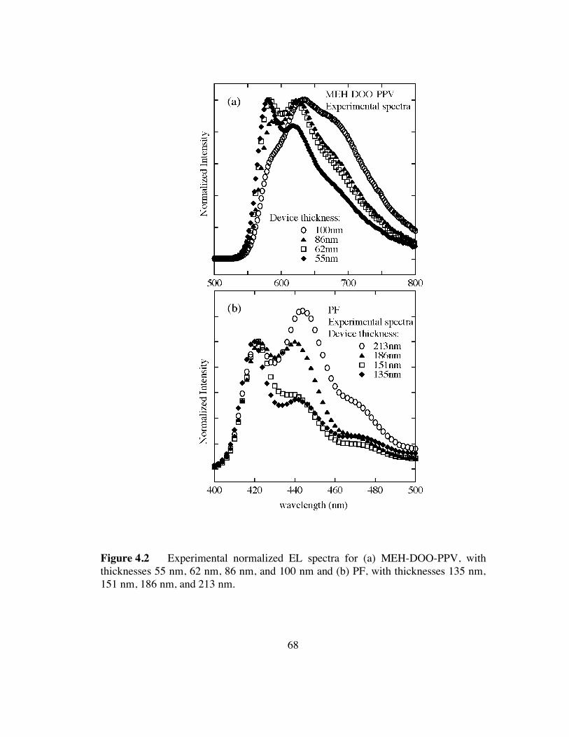
68
Figure 4.2 Experimental normalized EL spectra for (a) MEH-DOO-PPV, with
thicknesses 55 nm, 62 nm, 86 nm, and 100 nm and (b) PF, with thicknesses 135 nm,
151 nm, 186 nm, and 213 nm.

69
4.4 Simulation of interference effects in PLED structures
In order to understand the effects of optical interference on the properties of
polymer LED’s, we did simulations which model thickness dependence in single
layer polymer LED structures. Since polymer LED’s consist of a multilayer thin film
stack with a total thickness on the order of the emission wavelength, the emission
spectra critically depend on the thicknesses and refractive indices of the individual
layers. The theory underlying the simulations of interference effects used in this
study are described in section 2.4.
For our investigations, we assume that the emission zone location scales with
device thickness as expected if relative charge mobilities and injection rates remain
unchanged. The simulation parameters thickness, refractive index and basis spectra
were determined experimentally. For both the PF and the MEH-DOO-PPV, we use
an experimentally determined EL spectrum as the emission spectrum of the dipole.
The refractive index dispersion curves of MEH-DOO-PPV and PF were determined
by spectroscopic ellipsometry (VASE by Woollam Inc.). In particular, a Cauchy
dispersion model was fit to the transparent regime and subsequent extrapolation to
lower wavelengths was carried out by point-to-point fits. For this fit, an isotropic
model was chosen, thus ignoring birefringence in the films. The model gives a very
good fit to the experimental data. Inclusion of birefringence in the model is a subject
of future work. The resulting dispersion curves are shown in Figure 4.3.

70
Figure 4.3 Refractive index dispersion curves for MEH-DOO-PPV and PF.
For PEDOT-PSS, a constant refractive index value of 1.53 was assumed (Pettersson
et. al. 1998). The resulting simulated spectra are shown in figure 4.4(a) for the MEH-
DOO-PPV emission and in figure 4.4(b) for the PF. We can see that in both the
MEH-DOO-PPV and the PF simulations, for which we chose the same or similar
thicknesses as our experimental devices, the simulations very closely match the
experimentally determined spectra. We have shown that the simulations were

71
successful in modeling the changes in the relative weights of the two leading vibronic
peaks of the EL spectra with changing device thickness.
Figure 4.4 Simulated normalized EL spectra for (a) MEH-DOO-PPV, and (b) PF,
with various thicknesses.

72
In addition to simulating the EL spectra of these devices as a function of
device thickness, we looked at the radiance as a function of device thickness and
compared the experimental data to the simulated results. Those results are plotted as
figure 4.5(a) and 4.5(b). Experimentally determined values for radiance were
measured at the same current for all devices. Values plotted in figure 4.5 were
normalized to compare the relative changes in radiance with simulated results. The
overall trends in relative radiance with device thickness are nicely reproduced in the
simulated data.
We would expect that the trend in radiance with increased self-absorption
would be a steady decrease with increasing device thickness, and so we can conclude
that the observed trend in radiance is dominated by optical interference effects. In
addition, self-absorption should have the effect of decreasing the relative intensity of
the EL at wavelengths in the region of overlap between emission and absorption as
the thickness of the polymer layer is increased. As seen in figure 4.1, this region is in
both cases the leading vibronic peak in EL spectrum. Therefore the thickness
dependent effects seen in the experimental EL spectra are at least partially due to self-
absorption effects. However, the overlap is not large, and the difference in device
thickness is not significant enough to completely explain the strong thickness
dependence seen in the spectra of these devices. Again therefore, we expect that
interference may play the dominant role.

73
Figure 4.5 Experimental and simulated radiance curves in arbitrary units, for (a)
MEH-DOO-PPV and (b) PF. For the simulated results, emission is assumed to occur
20% of device thickness away from the anode.
4.5 Simulation of emission zone location
For both the PF and the MEH-DOO-PPV thickness dependence simulations
discussed above, we assumed the emission zone to be a distance 20% of the emissive
layer thickness away from the anode. To come to this assumption, it was necessary to
explore the dependence of the simulations on location of light emission. These
74
simulations are shown in figures 4.6 and 4.7. First we explore several emission zone
locations for a given device thickness in figure 4.6. Figure 4.6(a) shows a simulated
100nm thick MEH-DOO-PPV device, with light emission occurring at various
locations in the polymer layer. As the emission moves from the anode to the cathode,
we see an increase in the first peak intensity as well as a slight blueshift in peak
location. In contrast, the dependence on emission zone location for PF, shown in
figure 4.6(b) for a 190 nm thick device, does not display a clear trend. We see that
the emitted spectra for PF are highly sensitive to modest changes in emission zone
location.
Figure 4.7 shows the thickness dependent simulations recalculated under the
assumption that the emission is occurring nearer to the cathode. In figure 4.7(a), the
MEH-DOO-PPV simulation is done assuming emission to be a distance 70% of the
emissive layer thickness away from the anode. In this case, the thickness dependent
trend seen in the experimental data is reproduced; however, the effect in simulation is
less dramatic than seen in the experimental data. In figure 4.7(b), the PF simulation is
done assuming emission to be a distance 80% of the emissive layer thickness away
from the anode. Clearly in this case the thickness dependent trend seen in the
experimental data is no longer accurately reproduced. The emission location
parameter used in the simulations of thickness dependence in MEH-DOO-PPV and in
PF devices were chosen such that the resulting simulated spectra and radiance trends

75
most closely matched those seen in our experimental results. For both materials this
value is 20% of the polymer layer thickness from the anode.
Finally, we consider whether recombination near the anode is consistent with
our understanding of the device architecture. For PF*, electron injection from the
calcium cathode (work function ~ 2.9 eV) to the LUMO of PF (3.0 eV) is nearly
Ohmic; however, a large barrier to hole injection exists from the PEDOT-PSS (5.1
eV) to the HOMO of PF (5.8 eV) (Janietz et. al. 1998). For PF without endcaps, it is
thought by some that this barrier to hole injection causes electron-hole recombination
to occur directly at the polymer/PEDOT-PSS interface. The endcaps appear to assist
in hole injection into PF (Miteva et. al. 2001), moving recombination slightly into the
bulk of the material, increasing device efficiency and decreasing aggregation peaks
associated with the polymer morphology at the interface (Nakazawa et. al. 2002). It is
therefore reasonable to assume in this scheme that recombination should occur near to
the device anode, and light emission occurring at 20% of the polymer layer thickness
from the anode would then be consistent with this assumption. However, there has
been some evidence (Campbell et. al. 2002) that the lower electron mobility in PF’s
inhibits movement of electrons through the film toward the anode significantly
enough that despite a barrier to hole injection at the interface, recombination may be
occurring nearly at the cathode. In this scheme then, our assumptions are no longer
accurate, and therefore our simulations do not provide a close match to experiment.
In the case of PF materials, a straightforward conclusion about the location of

76
recombination may not be possible based on injection barrier and mobility arguments
alone.
In contrast, for MEH-DOO-PPV*, both the HOMO (5.3 eV) and LUMO (3.0
eV) levels are closely matched to the electrodes (Campbell et. al. 1996), providing
nearly Ohmic contacts for both electron and hole injection. As a consequence, we
would expect to see emission occurring at a thickness consistent with experimentally
determined relative charge mobilities in the material. Due to its similarities with
MEH-PPV, the hole mobilities for MEH-DOO-PPV should be on the order of, or
slightly higher than, the electron mobilities (Bozano et. al. 1999). This would suggest
that recombination should occur close to the center or cathode side of the device
rather than near to the anode (Malliaras et. al. 1998). However, the simulations of
thickness dependence in MEH-DOO-PPV show rather low emission zone location
sensitivity, and it is while it may not be the closest match to experiment, a simulation
using an emission zone located closer to the cathode would still provide a reasonable
simulation of MEH-DOO-PPV device thickness dependence.

77
Figure 4.6 Simulated normalized EL spectra for single device thickness as a
function of emission zone for (a) 100 nm MEH-DOO-PPV device, with emission
occurring at 10 nm, 30 nm, 70 nm, and 90 nm from anode, and (b) 190 nm PF device,
with emission occurring at 38 nm, 76 nm, 114 nm, and 152 nm from anode.

78
Figure 4.7 Simulated normalized EL spectra for (a) MEH-DOO-PPV, with
thicknesses 55 nm, 62 nm, 86 nm, and 100 nm and emission assumed to occur 70% of
device thickness away from the anode, and (b) PF, with thicknesses 130 nm, 150 nm,
190 nm, and 210 nm, and emission assumed to occur 80% of device thickness away
from the anode.

79
4.6 Conclusions
Several aspects of the simulations make it rather difficult to exactly reproduce
the experimental data. As previously mentioned, the choice of dipole emission
spectrum can significantly alter the overall appearance of the simulated spectra. In
addition, the simulation can be rather sensitive to parameters that are experimentally
determined, such as the thickness of both the hole injection layer and the polymer
layer, and are therefore subject to experimental errors in comparing with experiment.
Finally, assumptions are made in the calculations concerning the nature of charge
recombination, exciton diffusion, and emission zone location which are not fully
understood but which can change the final simulated thickness dependent effects. We
note that in polymer LED’s as discussed here, the emission zone may extend over a
few tens of nanometers. Thus the above model with an exact dipole location is an
approximation (Wan et. al. 2000). However, the simulations are able to illustrate that
the changes in the optical properties of polymer LED’s seen as a function of device
thickness can be well accounted for by simulation of optical interference effects.
*Values given for HOMO/LUMO energy levels are those corresponding to the closely
related materials PFO and MEH-PPV. We expect the true values to be very similar to
those reported.

80
CHAPTER 5
RECOMBINATION PROFILES IN MEH-PPV LIGHT-EMITTING
ELECTROCHEMICAL CELLS
5.1 Abstract
We present a study on the optical and electronic properties of light-emitting
electrochemical cells (LECs) based on poly[2-methoxy-5-(2-ethylhexyloxy)-1,4-
phenylenevinylene] (MEH-PPV) with the goal of understanding the emission profiles
in vertical device structures and characterizing their salt and electrode dependence.
Photoluminescence and electroluminescence profiles of planar LECs were directly
imaged as they varied with applied voltage, and simulations of interference effects in
multilayered device structures were performed in order to gain insight into emission
profiles in vertical structure LECs. While our results are consistent with oxidative
doping, they imply a lack of reductive doping in LECs under normal operating
conditions. We observe that trends in emission profiles for vertical structure LECs
follow those reported in planar structures and are independent of thickness, salt and
electrode type. In addition, device I-V and radiance characteristics were measured as
a function of salt and electrode type. Al electrodes resulted in variations in the I-V
characteristics and turn-on voltage due to oxidation of aluminum contacts as
compared to devices with Au contacts. Device performance was mainly independent

81
of anion selection; however, substantial changes in rectification were observed for
different cations. Finally, we discuss the implications of our findings on the
operating mechanism of LECs.
5.2 Introduction
Polymer light-emitting electrochemical cells (LECs) were first introduced by
Pei et. al. in 1995 (Pei et. al. 1995). In an LEC, a thin film of light-emitting polymer
admixed with an ionic conductor (typically polyethylene oxide, or PEO) and a salt, is
sandwiched between two electrodes. According to the initial proposed operating
mechanism, an applied voltage leads to electrochemical doping of the polymer, p-
type near the anode and n-type near the cathode, leading to the in situ creation of a
light-emitting pn-junction (Pei et. al. 1995, Pei et. al. 1996). Charge injection is then
facilitated through the creation of Ohmic contacts between the electrodes and the
highly conductive doped states of the polymer. The LEC was shown to operate in
both forward and reverse bias, effectively independent of electrode work function, at
voltages just above the polymer bandgap, consistent with the properties expected
from a dynamically reversible pn-junction (Pei et. al. 1995, Pei et. al. 1996, Li et. al.
1999, Smith 1997, Riess and Cahen 1997).
In 1998, deMello et. al. proposed an alternate theory also capable of
explaining these observed properties of the LEC (deMello et. al. 1998). They claimed
that the accumulation of ions at the electrode-polymer interfaces introduces large

82
electric fields that reduce the barriers to charge injection (deMello et. al. 1998,
deMello et. al. 2000). Thus electrochemical doping is not responsible for charge
injection in the LEC. Further, they claim that any electrochemical doping present in
an LEC under normal operation is unlikely (deMello et. al. 1998). Subsequent studies
reporting direct photoluminescence (PL) and electroluminescence (EL) imaging in
planar LEC structures, however, show a region of quenched PL that clearly indicates
the presence of doped polymer (Pei et. al. 1996, Dick et. al. 1996, Gao and Dane
2003, Gao and Dane 2004). These results would seem to suggest that the model
presented by Pei et. al. is the more likely picture; however, direct evidence that this
model is accurate and complete is still lacking.
Recently, we have presented an in-depth study of electrochemical doping in
MEH-PPV (Holt et. al., submitted), one of the most commonly used light-emitting
polymers for LEC studies. We have shown that while p-doping of this material is
highly reversible, efficient, and effectively independent of anion type, n-doping in
MEH-PPV is characterized by low efficiency in most cases and inherent instability in
all cases. Further, it has been shown that lithium salts are effectively incapable of n-
doping MEH-PPV using acetonitrile at room temperature (Holt et. al., submitted), an
observation supported by the observation that n-doping with alkali salts in
polythiophenes and polyacetylene is not possible except when the ionic radius is
increased with judicious solvent selection (Mastragostino and Soddu 1990, Zotti et.
al. 1995). Lithium triflate is the primary salt used in studies of polymer LECs. It is

83
thus highly doubtful that n-doping is strictly necessary for the operation of typical
MEH-PPV LECs, such as those presented in many previous works. Indeed,
convincing evidence of n-doping in an LEC or pLEC structure at room temperature
has yet to be presented. Clearly, further clarification concerning the fundamental
operating mechanism is necessary for a full understanding of the polymer light-
emitting electrochemical cell.
Surprisingly, light-emitting electrochemical cells have been little explored
systematically, considering their potential for use in air-stable displays and the
controversy surrounding their operating mechanism. Experimental results have been
limited primarily to a single structure (ITO/polymer:PEO:Li salt/Al). In particular,
there have been no systematic studies done on the effects of different salts and
electrode materials on the electrical and optical properties of the LEC. Finally, planar
structures have been well studied but the results obtained for these structures have not
been correlated to trends in vertical structure LECs to allow the generalization of
these important results.
In this work, we built both vertical and planar geometry LECs using MEH-
PPV as the emissive material. Devices were varied by salt type, salt concentration,
operating voltage, and electrode type. For the planar devices, in situ
photoluminescence and electroluminescence profiles were directly imaged using a
confocal microscope and CCD camera. For the vertical geometry devices, EL spectra
are measured in both forward and reverse bias, in addition to typical current-voltage
84
and radiance-voltage characterization. We use simulations of interference effects in
multilayered device structures using parameters obtained by observing emission
profiles in pLECs to predict emission profiles and compare with experimental results.
Finally, we discuss implications regarding the underlying operating mechanism of the
LEC.
5.3 Experimental details
Both planar and vertical geometry LECs were constructed using MEH-PPV
provided by American Dye Source as the emissive material. All polymer solutions
consisted of MEH-PPV and PEO in a 9:4 ratio, and salt in varying amounts, in
chlorobenzene. Salts used include lithium trifluoromethanesulfonate (triflate),
tetrabutylammonium (TBA) tetrafluoroborate (BF4), TBA hexafluorophosphate (PF6),
and TBA-triflate. Planar geometry LECs used a lower molecular weight (!100,000)
PEO to minimize phase separation while the vertical geometry LECs used higher
molecular weight (!5,000,000) PEO to achieve thicker films. After spin-casting,
films were annealed at 80oC for 3 minutes in an inert atmosphere, and placed under
vacuum (!10-7 Torr) overnight. Film thicknesses were measured on a Park Scientific
Autoprobe CP Atomic Force Microscope (AFM) and showed a variation of +/- 15
nm.
Planar geometry LECs were fabricated by evaporating gold strips onto glass
substrates after prior masking with a 15 µm fine wire. Carefully removing the wire
85
resulted in a clean gap of !20 µm thickness as determined by AFM. A polymer
solution was then spin-cast onto the substrate, annealed at 80oC for 3 minutes in an
inert atmosphere, and placed under vacuum (!10-7 Torr) overnight. Prior to testing,
the devices were encapsulated under inert atmosphere under a glass slide using
Addison Clear Wave AC A1425 UV curable epoxy. Contact to the electrodes was
made using copper tape with conducting adhesive. Images of PL and EL were
obtained using a 40x oil immersion lens on a Technical Instruments K2 SBIO
confocal microscope with a QImaging micropublisher CCD camera. The
photoluminescence source was an Osram HBO-100 W/2 mercury short arc photo
optic lamp with a rhodamine filter.
The vertical geometry LEC devices were prepared by spin-casting polymer
solution to a thickness of !350 nm onto pre-patterned ITO glass substrates. Top
electrodes were deposited by thermal evaporation. All device testing took place in a
dry nitrogen glove box using a Keithley 2400 Sourcemeter, a picoammeter, and a
calibrated silicon photodetector. Electroluminescence spectra were also taken in an
inert nitrogen atmosphere with an Ocean Optics fiber optic spectrometer.
5.4 Planar geometry LECs
Planar geometry LECs were constructed as shown in figure 5.1 using various
salt types and with an average width of ~20 µm. Images of the device
photoluminescence and electroluminescence profiles were captured using a confocal

86
microscope and CCD camera as described above. We found that the salt type made
little difference in the general results despite significant differences in the type and
size of the anions (triflate- vs BF4-) and cations (Li+ vs TBA+). The 0 V
photoluminescence, 3 V bias photoluminescence, and electroluminescence at 10 V of
a representative device are shown in figure 5.2.
Figure 5.1 Device structure of a planar geometry light-emitting electrochemical
cell.
As the applied voltage is increased, PL quenching can be observed at the
anode beginning as low as 1 V, indicating oxidative doping. Edman et. al. show that
the onset of p-type doping at voltages well below the bandgap of the material in
planar LEC structures is due to the location of the gold work function relative to the
HOMO/LUMO levels of the polymer (Edman et. al. 2004). Of particular interest is
the observation that no evidence of PL quenching occurs at the cathode, suggesting a

87
Figure 5.2 The 0 V photoluminescence, 3 V photoluminescence, and 10 V
electroluminescence of a planar LEC with TBABF4 salt.

88
lack of reductive doping in the device under normal operation. Previous groups have
suggested that the lack of distinct PL quenching at the cathode is due rather to low
concentrations of doped material or that PL quenching may be less efficient in n-
doped than in p-doped polymer, although a clear argument is not given in either case
(Pei et. al. 1996, Gao and Dane 2003).
At 3 V, the PL is highly quenched to within ~10% of the polymer layer
thickness from the cathode. As the bias is increased, the quenched region moves
toward the cathode as noted by other groups. The precise location of the
quenched/unquenched interface varied significantly from device to device but
occurred typically between 10%-40% of the device width away from the cathode. It
is possible that this location is highly sensitive to variations in salt concentration. In
our findings, the region of EL always occurred on the anode-side edge of the
unquenched region with a characteristic width of ~ 1/14 – 1/16 of the device
thickness. This could be due to the creation of a pn-junction within the device, or
could suggest that charge recombination may be limited by hole injection from the p-
doped polymer into the undoped region.
The ability to directly image the photoluminescence and electroluminescence
profiles of planar LEC structures has provided very important information that may
help to understand the operating mechanism of LECs. It is reasonable to assume that
in general the devices in planar and vertical geometry operate under the same basic
principles (Wenzl et. al. 2002); however, observations of planar devices are limited in

89
several important respects. First, the planar devices necessarily are restricted to using
the same material for both electrodes, disallowing the study of device operation in the
presence of a built-in electric field. Second, the imaging of these devices takes place
outside of inert atmosphere. This requires some kind of encapsulation and exposure
to air, both of which may affect device operation and prevents the successful study of
devices with electrodes, which are oxygen sensitive such as Al or Ag.
Finally, the construction of devices with such drastically different geometries
may result in a very different electric field profile within the device. In order to make
conclusions from the observations of planar LECs we desire some evidence that the
basic observed properties of the planar devices are duplicated in the vertical devices,
and then extend the study to include devices with variations in thickness and
electrode work functions. Unfortunately the vertical geometry prevents the direct
observation of emission and photoluminescence profiles, requiring the study of these
properties via a less direct approach.
5.5 Simulating interference effects in vertical geometry LECs
In order to investigate emission profiles in vertical geometry LECs, we did
simulations which model interference effects in single layer polymer light-emitting
device structures (ETFOS Emissive Thin Film Optics Simulator provided by B.
Ruhstaller). Since polymer LECs consist of a multilayer thin film stack with a total
thickness on the order of the emission wavelength, the emission spectra critically

90
depend on the charge recombination profile within the polymer layer, in addition to
the layer thicknesses and refractive indices of the individual layers. In the previous
chapter, we used simulations of interference effects to investigate the dependence of
polymer light-emitting diodes on polymer layer thickness (Leger et. al. 2003). The
simulation technique is based on a transfer matrix formalism with an oscillating point
dipole source and is described in further detail there.
The simulation parameters thickness, basis spectra, refractive index, and
emission profile were determined experimentally. In particular, the layer thicknesses
of our experimental devices were measured with AFM and the resulting values used
in simulation. We use the EL spectrum of a very thin (30 nm) MEH-PPV LED as the
emission spectrum of the dipole. The spectral features of such a thin device were
found to be effectively independent of interference effects as determined via
simulation and thus suitable as a basis spectrum for this application. The refractive
index dispersion curves of MEH-PPV:PEO were measured by spectroscopic
ellipsometry (VASE by Woollam Inc.) and are shown in figure 5.3.
For the emission profile, we use a gaussian distribution of dipole locations
with a characteristic width of 1/15 of the polymer layer thickness. This value was
obtained by observing the typical width of the EL emission in our planar LEC
devices. We make the assumption that the width of the emission profile scales with
device thickness as observed by others (Gao and Dane 2003). After defining the
parameters within the simulation software to match those measured for the
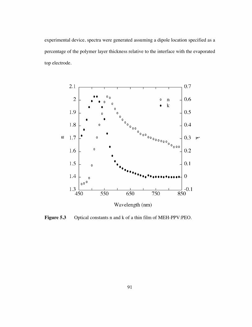
91
experimental device, spectra were generated assuming a dipole location specified as a
percentage of the polymer layer thickness relative to the interface with the evaporated
top electrode.
Figure 5.3 Optical constants n and k of a thin film of MEH-PPV:PEO.

92
5.6 Comparison of simulation and experiment: EL spectra of MEH-PPV
LECs
The experimental and most closely matched simulated EL spectra for three
different devices and various operating voltages are shown in figures 5.4 through 5.7.
Figure 5.4 compares spectra for a 500 nm device with Au top electrodes and figure
5.5 shows similar results for a 300 nm device with Al top electrodes. In both cases,
the best simulation results were obtained by assuming the location of light emission
to be approximately 30% of the device thickness away from the cathode for both
forward and reverse bias. It should be noted that, as with the planar LECs, no
noticeable dependence of the emission profiles were observed for variations in salt
type.
Figures 5.6 and 5.7 compare experimental and simulated EL spectra for a
250nm thick device with Au top electrodes. Figure 5.6 shows forward and reverse
bias while figure 5.7 shows spectra for high and low reverse bias voltages. For this
device, emission occurs symmetrically at approximately 10% of the layer thickness
away from the electrodes and shifts toward the cathode by about 4% of the polymer
layer thickness upon increasing the applied voltage from –4 V to –8 V.
The precise location of the symmetric light emission as a fraction of the
polymer layer with respect to the electrodes varies a significant amount for each
simulated device but typically fell in the range of 10% to 30%. This number clearly
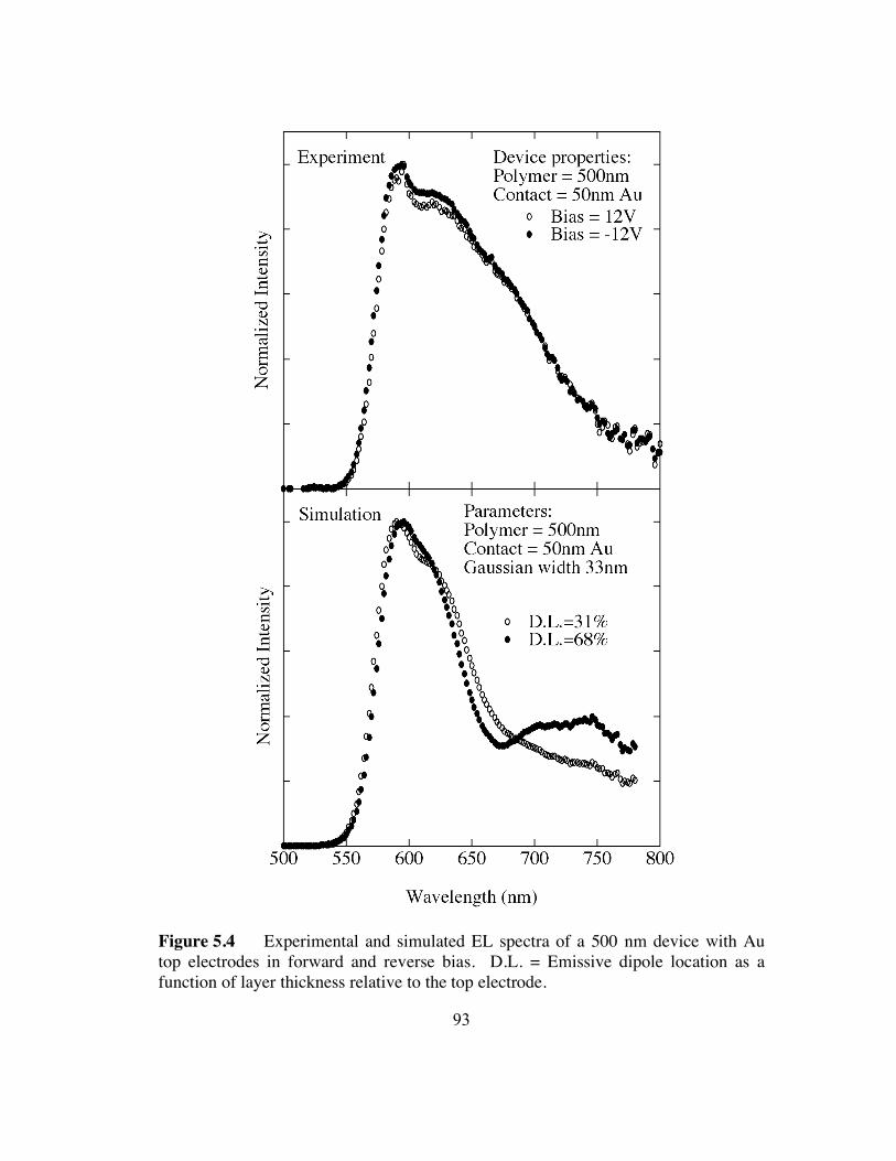
93
Figure 5.4 Experimental and simulated EL spectra of a 500 nm device with Au
top electrodes in forward and reverse bias. D.L. = Emissive dipole location as a
function of layer thickness relative to the top electrode.

94
Figure 5.5 Experimental and simulated EL spectra of a 300 nm device with Al top
electrodes in forward and reverse bias.
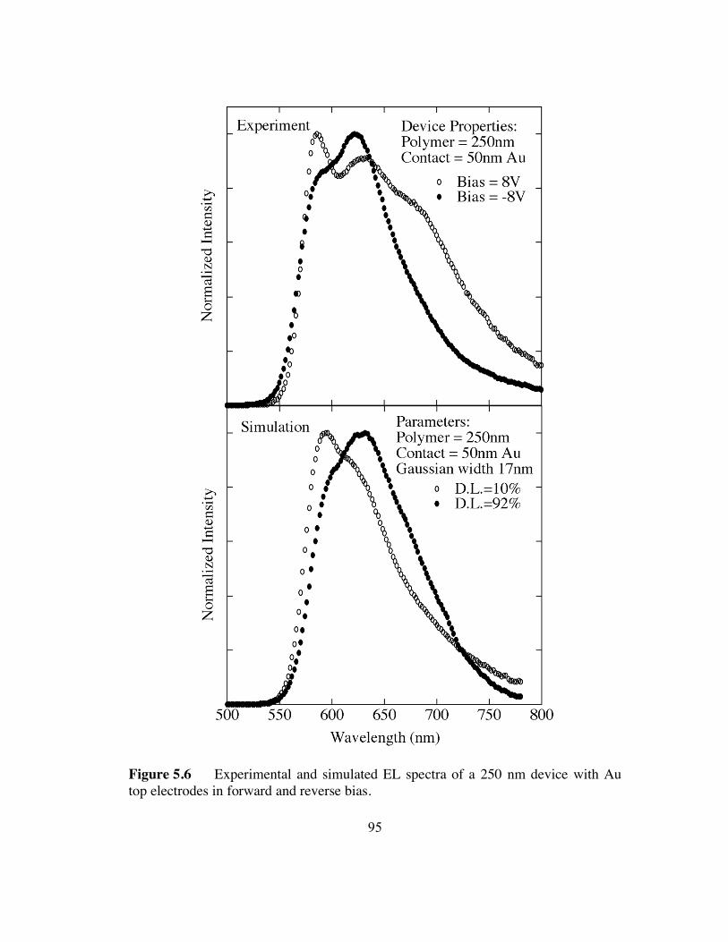
95
Figure 5.6 Experimental and simulated EL spectra of a 250 nm device with Au
top electrodes in forward and reverse bias.

96
Figure 5.7 Experimental and simulated EL spectra of a 250 nm device with Au
top electrodes in high and low reverse bias.

97
varied with the applied voltages at which the spectra were obtained, but also varied
significantly from device to device, suggesting that the location of light emission in a
given device is highly sensitive to slight changes in the device preparation. It should
be noted that the variation in emission location for the vertical structure LECs as
determined by simulation is of a similar range as the variation seen for the planar
structures. For reference, figure 5.8 shows simulated EL spectra for a 300 nm device
with an Al top electrode as a function of dipole location within the device. The
variation is quite dramatic and in nearly all cases the match to the experimental
spectra for a given voltage was unique to one specific emission location. We can
therefore assume that the predicted emission locations are correct.
Figure 5.8 Simulated EL spectra of a 300 nm device with Al top electrodes as a
function of emission location throughout the polymer layer.

98
In general, the comparison between the experimental voltage-dependent EL
spectra and simulations of these spectra show excellent correlation when we assume a
gaussian dipole emission with a characteristic width of about 1/15 of the polymer
layer thickness centered an approximately equal distance from the cathode and anode
in forward and reverse bias respectively. These results therefore successfully
reproduce the trends in emission profile as determined experimentally for the planar
devices for each device. Further, they indicate that the voltage-dependent trends in
emission profiles are general with respect to polymer layer thickness and top
electrode work function. The simulation of optical interference effects in vertical
geometry polymer light-emitting electrochemical cells therefore show remarkably
strong evidence that the various results demonstrated for planar structure LECs can be
generalized to vertical structure devices.
5.7 Electrical and optical characterization of vertical geometry LECs
In order to further characterize our vertical geometry LECs with respect to top
electrode and salt type, we took current-voltage and radiance curves for several
devices. The devices were held at the maximum range of positive or negative
voltages until fully charged and stable light output was achieved prior to scanning. A
1.5 second delay between voltage step and current-radiance measurement was
introduced to compensate for the slow device response. Typical I-V curves for a

99
Figure 5.9 Current-voltage curves for LECs using Li triflate and both Au and Al
top electrodes. Devices were first charged at high positive or negative voltages prior
to voltage sweep.

100
vertical structure LEC with Au and Al top electrodes are shown in figure 5.9. Using
an Au top electrode, the devices display remarkably symmetric diode-like I-V
characteristics that are fairly independent of charging voltage. For the device with Al
top electrode, however, the I-V curves show much stronger dependence on charging
voltage.
In chapter 6, we show that the reversibility of oxidation in MEH-PPV
depended strongly on the tendency of the electrode on which the doping took place to
oxidize. Specifically, the reversibility of p-doping in MEH-PPV films on Al
substrates in an oxygen reduced, but not inert, atmosphere was very low. When
charging in forward bias, the oxidation takes place at the ITO interface. As the scan
reaches high negative potentials, the current decreases, possibly due to some
oxidation occurring of the Al electrode. When charging at negative voltages,
oxidation occurs at the Al interface. Presumably the low oxygen levels present in the
inert atmosphere result in only a limited oxide layer on the Al and thus in steady state
reverse bias the device current is uncompromised. As the device is scanned to
positive voltages a feature appears in the I-V curve that may be attributed to the
reversal of the oxidation in the Al electrode that results in a temporary decrease in
device current.
Figure 5.10 shows radiance-voltage curves for two LEC devices with Au and
Al top electrodes. The device with Au top electrode showed lower turn-on voltages
in reverse bias than the device with Al top electrode, also indicating a possible

101
process such as oxidation of our top electrode in reverse bias, occurring for Al but not
for Au. Although the devices were placed in high vacuum overnight and tested in an
inert nitrogen atmosphere, evidence suggests the presence of some minor oxide
formation of the Al contacts in both the I-V and radiance data. If the differences in
these devices were due simply to the difference in electrode work functions, we
would expect to see more straightforward differences in the I-V and radiance
characterization such as similar shapes but shifted turn-on voltages in both directions.
This sensitivity of the device behavior to the presence of minor amounts of oxygen
has implications for the light-emitting displays constructed with air-stable top
electrodes such as Al or Ag.
Figure 5.11 shows the radiance curves for LECs with various salts. The
device made using Li triflate shows much lower turn-on voltages in reverse bias than
those with TBA cations after charging at high positive voltages. It is possible that the
tendency of the TBA cation to reduce ITO at voltages lower than those necessary to
reduce MEH-PPV or a reduced mobility of the TBA cation could be affecting the
device turn-on in reverse bias.

102
Figure 5.10 Radiance-voltage curves for devices using Li triflate and Au or Al top
electrodes.
Figure 5.11 Radiance-voltage curves for devices using various salts and Au top
electrodes.
103
5.8 Discussion and Conclusions
We have reported a study on MEH-PPV based light-emitting electrochemical
cells that includes a study of the emission profiles in both planar and vertical structure
LECs and systematically explores device performance in LECs with various salt
types and top electrode metals. Planar geometry LECs were constructed and their
photoluminescence and electroluminescence profiles were directly imaged. Our
results confirm previously reported studies that p-doping occurs at voltages well
below the polymer bandgap (Edman et. al. 2004), that EL occurs with a characteristic
width at the edge of the region with unquenched PL and shifts toward the cathode
with increased voltages, and that no clear evidence of n-doping is seen under normal
operating conditions, even with TBA salts which have been shown to be effective in
n-doping MEH-PPV.
We performed simulations of optical interference effects in multilayered
device structures to predict emission profiles in vertical structure LECs and found that
the results correlated surprisingly well with those results presented for planar devices.
We showed further that these results are general with respect to polymer layer
thickness, top electrode choice, and salt type.
Finally, we characterized the optical and electronic properties of LECs and
found that the I-V characteristics and light emission depend strongly on the choice of
top electrode and salt cation. In particular, devices with Au top electrodes and Li
salts show highly symmetric diode-like I-V curves and symmetric turn-on behavior.

104
Devices with Al top electrodes show sensitivity to oxidation of the top contact even
when tested in inert atmosphere which affects the I-V curves and causes delayed
emission in reverse bias. Devices using TBA salts also show delayed and reduced
emission in reverse bias.
Recent results in the study of the electrochemical doping process in MEH-
PPV have highlighted the need to revisit the issue of the operating mechanism of the
LEC for which electrochemical doping is thought to be central to the operation of the
device. The results of studies on planar LECs under normal operating conditions in
combination with studies showing that Li triflate, a commonly used salt in LEC
applications, does not n-dope MEH-PPV in most cases, suggest that n-doping is not
strictly necessary for the operation of the LEC. The simulation results allow us to
generalize these results to vertical LECs with a variety of salts and electrodes. We
strongly suspect that the inclusion of dipole effects at the polymer-cathode interface
are in fact necessary to fully explain the efficient electron injection seen in these
devices and successfully model the LEC operating mechanism.

105
CHAPTER 6
ELECTROCHEMICAL AND OPTICAL CHARACTERIZATION OF p- AND n-
DOPED MEH-PPV
6.1 Abstract
We study electrochemical p- and n-type doping in the well-known light-
emitting polymer MEH-PPV (poly [2-methoxy-5-(2-ethylhexyloxy)-1,4-
phenylenevinylene)]). Doping reactions are characterized using cyclic voltammetry.
Optical measurements including photoluminescence and UV/Vis/NIR transmission
were performed on doped samples. We find that oxidation in MEH-PPV is a highly
reversible reaction resulting in stable free-standing doped films, while the reduced
form is unstable and the reaction irreversible. We discuss the dependence of doping
reactions on scan rate, film thickness, salt type and concentration, and working
electrode type. We observe the development of two additional broad absorption
bands in both lightly and heavily doped films accompanied by a slight blue-shift in
the primary optical transition suggesting bipolaron band formation. Finally we find
that doping results in extremely sensitive photoluminescence quenching. We
propose a physical model for understanding electrochemical doping in MEH-PPV and
the implications this has on the development of such technologies as polymer light-
emitting electrochemical cells, electrochromic devices, actuators and sensors.

106
6.2 Introduction
The soluble derivatives of poly(phenylene vinylene) PPV are useful for
studying the mechanical and electrical characteristics of luminescent, conducting
polymers. One of the most well studied soluble PPV derivatives is MEH-PPV (poly
[2-methoxy-5-(2-ethylhexyloxy)-1,4-phenylenevinylene)]). Commended for its ease
of use, reproducibility and versatility, MEH-PPV is widely used in the study of many
applications such as organic polymer photovoltaics (Yu et. al. 1994), light emitting
diodes (Friend et. al. 1990, Braun and Heeger 1992, Parker 1994), and LECs (Yang
and Pei 1996, Santos et. al. 2001), as well as a water soluble version in biosensors
application (Chen et. al. 1999). In the work presented in chapter 7, MEH-PPV was
the material of choice for a solid-state electrochromic device because of the sharp
contrast in color between doped and undoped states (Holt et. al. 2005).
Understanding the factors affecting doping reactions and the effects that doping
have on the characteristics of the polymers are essential to the improvement of
existing technologies in which doping is a critical component of the operating
mechanism such as light emitting electrochemical cells (LECs) (Pei et. al. 1995, Pei
et. al. 1996), piezoelectric devices (Fukada 2000), and electrochromic devices (Monk
et. al. 1995, Mortimer 1999). That knowledge is equally valuable for application to
the development of novel technologies such as in biosensors, and integrated sensors
and displays.
The doping process in conducting polymers as currently understood introduces

107
deformations called solitons, polarons and bipolarons into the polymer system
causing new levels to form in the bandgap, increasing the amount of possible energy
transitions (Bredas and Street 1985, Baeriswyl et. al. 1992). Because polymers are
inherently disordered, it is difficult to characterize the fundamental roles of these
quasi-particles in the doping process. Many optical spectroscopic techniques are used
to explore doping in conducting polymers. We can better understand the dopant
deformations by utilizing these experimental techniques as well as studying
theoretical models.
There have been many studies on the electrochemistry of PPV and on the
optical properties of doped PPV using Raman spectroscopy (Baitoul et. al. 1997,
Baitoul et. al. 2000, Obrzut and Karasz 1987), UV absorption and infrared absorption
(Sakamoto et. al. 1994) as well as many studies on the electronic and electrochemical
properties of PPV and is derivatives (Voss et. al. 1991, Eckhard et. al. 1989, Cervini
et. al. 1997, Orion et. al. 1998). Despite the importance of MEH-PPV in devices,
studies on the electrochemical and optical characteristics of doped MEH-PPV (Santos
et. al. 1992) have been fairly limited in scope.
In this chapter, we present an electrochemical study of the p and n-doping
processes in MEH-PPV, and its affect on the absorption and photoluminescence
spectra of the polymer. Different methods were used to analyze the doping process of
MEH-PPV. Cyclic voltammetry is used to characterize and study redox reactions at
an electrode with regard to such properties as reversibility, stability and doping onset

108
values. UV/VIS/NIR transmission spectra and photoluminescence spectra were
obtained in order to examine the changes in optical transitions associated with p- and
n- type doping in MEH-PPV. This information is vital for example to the
development of optical sensors in which photoluminescence quenching is the
determining factor.
6.3 Experimental details
The polymer studied was MEH-PPV provided by American Dye Source.
MEH-PPV is an orangish-red colored, luminescent polymer easily solvable in
common organic solvents that exhibits a color change to greenish-brown when
electrochemically doped. Figure 6.1 shows the structure, absorption and
photoluminescence spectra of MEH-PPV.
Cyclic voltammetry experiments were performed using a non-aqueous
silver/silver ion reference electrode (Ag/Ag+, 0.3 V vs. SCE), a platinum counter
electrode and most often, a MEH-PPV/ITO working electrode. Other working
electrodes tested were MEH-PPV/gold, aluminum, and titanium nitride (TiN).
Substrates consisted of ITO glass substrates, provided by Thin Film Devices, TiN
substrates, and metals, gold, aluminum and silver, thermally deposited up to 50 nm on
glass. A polymer solution of MEH-PPV and chlorobenzene was then spun-cast on
the metal to the desired thickness. Following polymer deposition, all substrates were
annealed at 120 °C for one hour under vacuum and dried in a vacuum chamber

109
overnight. The electrolyte consisted of salts lithium trifluoromethanesulfonate (Li
triflate), tetrabutylammonium tetrafluoroborate (TBA BF4) or TBA triflate in
acetonitrile at 0.01 M and were purged with nitrogen prior to testing in order to
reduce oxygen contamination. Data was obtained on an EG&G Princeton Applied
Research Model 362 Scanning potentiostat and two 2010 Keithley mulitmeters. Film
thicknesses measurements were taken using a Thermomicroscope Autoprobe CP
atomic force microscope and typically have a variation of ~ 15 %.
Figure 6.1 MEH-PPV chemical structure, absorbtance spectra, and
photoluminescence spectra for film and solution.

110
Transmission spectra for p-doped films were taken on three machines each with
a different wavelength range to study the material from the visible region past the
near infra-red region. For wavelengths from 380 nm to 1200 nm, transmission
spectra were taken with a Perkin Elmer UV/Vis/NIR Spectrometer Lambda 9 and for
the in situ n-doped films, with a Varian Cary 3 spectrophotometer. A Perkin Elmer
Spectrum One Spectrometer was used for the range from 1100 nm to 3000 nm.
Although the data from each machine matched fairly well, to neatly plot the full
wavelength range for the p-doped films, the data from the Spectrum One was shifted
uniformly by no more than 6% of total absorption to match that from the Lambda 9 in
their overlapping region. The Photoluminescence spectra were acquired only on the
p-doped films using a Perkin Elmer Luminescence Spectrometer LS 45. The material
was excited at 505 nm, the undoped MEH-PPV absorption maximum. Solid-state
devices for photoluminescence and absorption experiments were constructed as
described in chapter 7 (Holt et. al. 2005).
For optical studies of p-doped MEH-PPV, removing films from the electrolyte
solution at the desired doping voltage produced films of different doping levels. The
p-doped films retained their characteristics indefinitely. However, optical spectra of
n-doped MEH-PPV films were more difficult to acquire as n-doped films are highly
unstable. They must be kept under constant potential and cannot be removed from
the electrolyte. Thus, in situ experiments were performed solely on one instrument in
a wavelength range from 380 to 900 nm.

111
6.4 Cyclic voltammetry results
Cyclic Voltammetry was the primary tool used to characterize doping in MEH-
PPV and was also used to produce doped films for transmission and
photoluminescence studies. In the redox reactions of an MEH-PPV film, counter ions
from the electrolyte diffuse into the material and allow the p and n doping of the
material. MEH-PPV is capable of being both p and n-doped and exhibits a color
change from orangish-red to greenish-brown (Santos et. al. 2002). With p-doping, the
anodic peak occurs at about 0.8 V (vs. Ag/Ag+) and the cathodic peak at about 0.4 V.
For voltages higher that 1 V, increases in the current indicate the onset of an
overoxidation peak that occurs around 1.3 V and results in the degregation of the
polymer. We performed experiments exploring the effects that the salt type and salt
concentration in the electrolyte have on the doping process as well as how the doping
of the material is affected by the working electrode type, the scan rate, and the film
thickness.
Anions tested in the p doping process were triflate-, tetrafluoroborate (BF4-),
hexafluorophosphate(PF6-), and sulfonate(SO4
-). When examining optical contrasts in
solid-state devices, we observed that organic anions were slightly more effective at p-
doping than inorganic ones. In the cyclic voltammetry experiment however, no
systematic differences were observed for different salts. This could be due to larger
errors in the cyclic voltammetry experimental setup or due to varying mobilities of
ions in the solid electrolyte of the solid-state devices.
112
Cations tested in the n-doping process were Li+ and TBA+. It has been
demonstrated that alkaline cations cannot effectively electrochemically n-dope
polythiophene or polyacetylene in certain solvents such as acetonitrile and propylene
carbonate due to their small effective ionic radius (Zotti et. al. 1995, Mastrogostino
and Soddu 1990). The cyclic voltammogram in figure 6.2 shows that there is no
redox reaction in the negative voltage range, suggesting that Li+ is unable to n-dope
MEH-PPV. Only slightly reversible n-doping accompanied by color change occurs
with the organic cation TBA+. It is understood that most polymers are
electrochemically unstable when n-doped due to redox reactions with water and
oxygen (deLeeuw et. al. 1997). An indication of the instability of n-doped MEH-PPV
was its inability to retain a change in color outside of the electrolyte.
Under a carefully monitored experimental setup, the highest occupied molecular
orbital (HOMO), and the lowest unoccupied molecular orbital (LUMO) energy levels,
of a conductive polymer can be approximated by the p and n-doping onset potentials
(Li et. al. 1999). We performed detailed studies on whether the electrodes, ITO, Au,
Ag, Al, and TiN onto which the polymer is deposited affect the onset potentials. As
expected, the onset potentials for n and p-doping, determined from the intercept of a
line tangent to half the largest slope value, for most of the electrodes varied no more
that 0.05 eV and suggest an electrochemical band gap of about 2.4 eV, corresponding
well with previous studies of single-particle energy gaps at 2.45 eV (Campbell et. al.
1996). The values of the onset potentials for electrodes Al and TiN, though are quite

113
Figure 6.2 Cyclic voltammetry setup and cyclic voltammagrams for various
MEH-PPV working electrodes with a) 0.01 M Li triflate and b) 0.01 M TBA BF4
electrolyte.

114
different possibly due to prior oxidation of the material. Using the methods employed
by Li et al. 1999 to calculate the HOMO and LUMO levels for MEH-PPV, the
average level for the HOMO was about -5.1 eV and for the LUMO, -2.7 eV. These
values, listed in Table 6.1 for various electrode materials, are similar to those
calculated by Y. Li et al. 1999 and R. Cervini et al. 1997.
p onset n onset HOMO LUMO
Electrochemical
bandgap
Electrode (V)a (V)a (eV)b (eV)b (eV)c reversiblityd
ITO 0.32 -2.10 -5.02 -2.60 2.42 n and p
Au 0.34 -2.00 -5.04 -2.70 2.34 n and p
TiN 0.49 -2.00 -5.19 -2.70 2.49 slightly in n
Ag 0.31 -2.00 -5.01 -2.70 2.31 n only
Al 0.60 -2.66 -5.30 -2.04 3.26 slightly in n
, , , das defined by visible color change
Table 6.1 Doping onset potentials, calculated HOMO/LUMO levels,
electrochemical bandgap, and qualitative reversibility for MEH-PPV on various
electrodes.
In a general, for a Nerstian system, a reversible redox reaction meets the criteria
that the peak potentials are independent of the sweep rate with a difference of 54 mV
between them and that the ratio of the current values at the peak potentials is unity.
The redox reaction of MEH-PPV is a quasi-reversible one. This is illustrated in
Figure 6.3 which shows that for higher scan rates, the anodic peak occurs at a higher

115
potential and the current increases. The increase in current for faster scan rates is a
result of charge conservation while the increase in anodic peak potential indicates that
the rate of reaction is comparable to the scan rate.
Figure 6.3 Cyclic Voltammogram for MEH-PPV at varied scan rates in 0.01 M Li
triflate electrolyte.
The reversibility of MEH-PPV depends on which type of metal is used for the
electrode. As depicted in figure 6.2, for p-doping using TiN, the cathodic peak has a
much lower current value than the anodic peak in contrast to ITO and Au which both
have more comparable peak heights. When n-doping, reversibility is higher for the

116
ITO electrode than TiN which has no anodic peak. We assign the second peak at -2.5
V for ITO as the cathodic peak for n-doping of MEH-PPV and assign the first peak to
reduction of ITO.
The difference in reversibility for the various electrodes may be due to the
oxidation of Al and Ag resulting in non-uniform color change of the film. No anodic
peaks were observed with p-doping for Ag and Al, only overoxidation onset and they
exhibited a color change reaction with small increasing fully doped regions that
afterwards, failed to return to their original color. It is possible that an oxide layer
formed on the metal prevents the uniform doping of the polymer material. The n-
doping reactions however, were slightly more reversible but showed similar features.
Although the doping onset potentials should not be affected by the experimental
setup, the position of the doping current peaks are affected by salt concentration in
the electrolyte and film thicknesses. Increasing salt concentration in the electrolyte
increases the reaction rate and occurs until the effects of ion pairing in the
concentrated electrolyte slow the reaction rate down (Holt et. al. 2005). This affects
the anodic and cathodic peak potentials and is the opposite effect to that of increasing
the film thickness. Due to reduced ion mobility, a thicker film exhibits a slower
reaction rate. Figure 6.4 exhibits the effects that film thickness and salt concentration
have on the anodic and cathodic peak positions. It should be noted that the onset
potentials, however, remain constant.

117
Figure 6.4 Cyclic Voltammograms for MEH-PPV for a) different film thicknesses
and b) varied salt concentration.

118
6.5 Absorption spectra at progressive doping levels
Upon oxidation, an electron is removed from the pi-system of the polymer
backbone leaving a positive spinless charge and a free radical. This spin !
combination, called a polaron, creates two energy levels inside the band gap, one
singly occupied, symmetrically placed around the center of the gap, as described in
Chapter 1. That single electron can also be removed creating a spinless bipolaron
with localized energy states farther from the band edges than the polaron states
because of the stronger lattice relaxation. Figure 6.5 displays the energy levels of
these quasi-particles as well as the possible energetic transitions. Within the
continuum electron-phonon-coupled model utilized by Fesser, Biship, and Campbell
(FBC model), w1 and w2 are the dominant transitions for the polaron and !1’ for the
bipolaron (Fesser et. al. 1983).
Figure 6.5 Illustration of the energy transitions for a) an undoped polymer, b) a
positive polaron and c) and positive bipolaron.

119
Theories and past experiments suggest that polarons are present in systems at
low doping levels while bipolarons are more favorable at higher doping levels (Patil
et. al. 1997). As shown in figure 6.6, we examine the absorption spectra of MEH-
PPV and observe two mid-gap transitions at high doping voltages, at about 1.74 and
0.67 eV, consistent with the theory of bipolaron formation. Figure 6.7 depicts these
transitions with w1’ = 0.67 eV and w3’= 1.74 eV which sum up to approximately
equal the band gap which peaks at about 2.45 eV. We observe a shift in spectral
weight from the band gap transition to the !1’ and !3’ bipolaron transitions as
expected. We also observe a blue shift of about 0.11 eV in the interband absorption
peak that accompanies the extremely broad low energy transition indicating the
formation of bipolaron bands within the gap that occurs with heavy doping (Bredas
and Street 1985).
Within the FBC model, the absorption coefficient and confinement parameter
are both functions of the ratio !0/"0 where !0 = (!3’ – !1’)/2 for bipolarons and "0 =
Eg/2. For MEH-PPV, the ratio w0/D0 = 0.44 and is consistent with previous
measurements (Voss et. al. 1991). However, the ratio of the intensities of the two
peaks I(w1’)/I(w3’) = I(0.67 eV)/I(1.74 eV) = 1 does not agree with I(w1)’/I(w3’) # 12
as predicted by the FBC model. This “intensity anomaly” has been frequently
discussed. Proposed explanations include theoretical drawbacks within the FBC
model or misallocated observed transitions.

120
Figure 6.6 Absorptance spectra for an MEH-PPV film at progressive doping
levels.
Figure 6.7 Illustration of bipolaron energy levels in MEH-PPV.

121
Also inconsistent with the polaron/bipolaron picture is the observation of only
two transitions in addition to the primary transition at low doping levels. As the
doping level increases, the lower energy transition at 1 eV disappears while the higher
energy one at 1.77 eV appears to either red shift 0.03 eV or be replaced by a different
optical transition at 1.74 eV. Since both transitions appear in the pristine spectra as
well as at lower doping levels, there may be other reasons for their appearance. The 1
eV transition is likely caused by a doping reaction between ITO and the MEH-PPV
film as it is not present when spectra are obtained on quartz while the higher energy
transition tends to be more prominent in thinner films and is likely due to aggregation
in the polymer film.
The issue of what is the most favorable defect (polaron vs. bipolaron) with
doping in conjugated polymers and their absorption signature is currently in debate.
The literature forming the main body of this debate is reviewed in Chapter 1, section
3. Our data suggests primarily bipolaron and bipolaron band formation because of
the values of the energy levels. It is a possibility that we are observing the
coexistence of polarons and bipolarons at heavy doping because of the inability to
distinguish several specific transitions within the broad low energy transition peak.
In that case, vibrational spectroscopy would be needed to distinguish the two.
We also performed limited range in situ absorption experiments in order to
obtain spectra for n-doped MEH-PPV films. Using MEH-PPV/ITO as the working

122
electrode, we observe reversible n-doping reactions. Figure 6.8 shows the spectral
progression and a color change is evident. There is a decrease in the intensity of the
interband transition peak accompanied by an increase in intensity of absorption at
lower energies for doping voltage values up to –2.4 V. Larger negative voltages
applied across the material resulted in n-doped films of greater instability and the data
acquired provided no new information. We see an additional peak forming with a
higher spectral weight at 2.9 eV likely caused by changes in the absorption spectra of
n-doped ITO. There also appears to be a peak forming between 1 and 1.5 eV.
However, this is not certain due to the limited energy range.
Figure 6.8 In situ obtained absorbtance spectra of n-doped MEH-PPV film.
123
6.6 Photoluminescence quenching
As MEH-PPV is doped, color change is preceded by a quenching affect in the
photoluminescence of the material. Figures 6.9 and 6.10 show that the
photoluminescence is sensitively quenched with doping level. For oxidative doping,
full quenching occurs at 0.35 V while visually, color change typically occurs at about
0.5 V. For reductive doping, PL quenching measurements were taken in situ due to
the unstable nature of the reduced films. For this data, full PL quenching is seen by
around -2.2V vs Ag/Ag+. Similar degrees of photoluminescence quenching with
doping occur in the solid state devices as well and the photoluminescence is fully
recovered upon dedoping. Photoluminescence quenching is expected for doped
MEH-PPV because as the material becomes more metallic, there are more states
available to which an exiton can non-radiatively decay. Photoluminescence
quenching due to electrochemical doping has been observed in polythiophene films
(Hayashi et. al. 1987) and similar effects due to photo-oxidation have been observed
in PPV films (Yan et. al. 1994) and MEH-PPV solution (Xiong et. al. 2004). The
sensitivity of the photoluminescence spectra to doping level is likely explained by the
observation that the effective size of the defect is much larger than its actual size for
trapping exitons and one defect is able to quench an entire polymer chain
(VandenBout et. al. 1997).

124
Figure 9 Photoluminescence spectra for MEH-PPV film at progressive
oxidative doping levels.
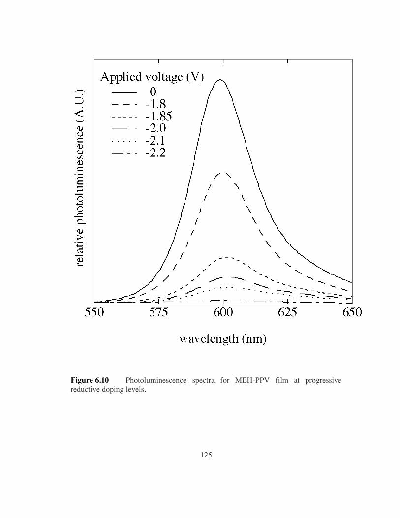
125
Figure 6.10 Photoluminescence spectra for MEH-PPV film at progressive
reductive doping levels.
126
An interesting effect occurs when attempting to n-dope the solid-state devices.
When using Li triflate, the photoluminescence of the material increases by up to 50%
with increasingly negative voltages down to -3 V. Hence it is possible that prior to
testing, there are already defect sites in the polymer film from reactions with ITO, as
studied by Werner et al. 1998, and compensated by charged ions. The application of
a voltage across the pristine device aids in the removal of these impurities from the
material thereby increasing its ability to photoluminescence. At higher doping
voltages, no resulting n-doping occurred as expected for Li triflate. On the other
hand, when using TBA triflate, initially the photoluminescence increases as with Li
triflate but thereafter proceeds to decrease slowly indicating the occurrence of
moderate n-doping in the polymer layer.
6.7 Conclusions
The electrochemical properties and doping processes of MEH-PPV, a useful
light-emitting soluble derivative of PPV, were extensively studied and the results of
the cyclic voltammetry experiments, absorption studies, and photoluminescence
studies were presented. Cyclic voltammetry curves of MEH-PPV illustrate the
dependence of the doping process on salt type, salt concentration, film thickness and
electrode type. Although the type of salt used has little effect on the process, the
quasi-reversible doping reaction of MEH-PPV is susceptible to changes in salt
concentration and film thickness which affect the speed of the reaction.

127
Theoretically, electrode type should not effect the doping onset potentials as they
reflect the HOMO and LUMO levels of the polymer and was observed for the most
part in agreement with other experimental studies. However, oxygen sensitivity does
affect the onset potentials for electrodes Al and TiN.
Throughout the doping process, transmission and photoluminescence spectra
were taken. The absorption spectra indicate the formation of bipolarons with heavy
doping. Other transitions observed at low doping levels were attributed to aggregation
and reactions with substrate ITO. In situ transmission and photoluminescence data
was obtained for n-doped MEH-PPV films which has not before been published or
studied. Photoluminescence in MEH-PPV was much more sensitive to doping level
than the absorption and was observed to be almost entirely quenched prior to visible
color change in agreement with observations that one defect is able to create a
quenching site the size of an entire chain.
128
CHAPTER 7
SOLID-STATE ELECTROCHROMIC DEVICES BASED ON PPV POLYMERS
7.1 Abstract
We present a solid-state electrochromic device structure employing a PPV-
based light-emitting polymer and explore device performance as a function of salt
type, salt concentration, and polymer layer thickness. Devices display high
reversibility, dramatic optical contrasts, and low operating voltages comparable to
state of the art conducting polymer electrochromic devices. Salts employing organic
anions display slightly improved optical contrasts. Thicker devices, higher voltages,
and higher salt concentrations produce higher optical contrasts at the cost of slowed
switching speeds. Understanding the factors affecting doping in PPV-based polymers
is crucial for the development of applications such as polymer LECs, actuators, and
sensors.
7.2 Introduction
Soluble light-emitting polymers based on poly (phenylene vinylene) (PPV)
have been extensively studied for their use in applications such as light-emitting
diodes (Burroughs et. al. 1990, Friend et. al. 1999) and photovoltaic cells (Tang 1986,
Brabec et. al. 2001); however, understanding doping effects in these materials have

129
largely been limited to light emitting electrochemical cells (Pei et. al. 1995. Pei et. al.
1996). This is surprising since doping can be used for controlling a wide variety of
other interesting properties, including electrochromic (Monk et. al. 1995, Mortimer
1999) and piezoelectric effects (Fukada 2000). In particular, the ability to control
electrochromism in electroluminescent polymers opens up wide range of potential
technologies for novel integrated sensors and displays.
We discuss the construction of a solid-state electrochromic device employing a
PPV-based light-emitting polymer as the color-changing material. We show that the
color changes observed for PPV-based materials have properties comparable to the
best and most widely studied polymer electrochromic materials, such as polypyrrole
and polythiophene (Lu et. al. 2002, DePaoli et. al. 1990, Garnier et. al. 1983). By
studying changes in the electrochromic properties as a function of doping
concentration and type and device thickness, we propose a model for understanding
and optimizing the effect of doping on the absorption in PPV-based materials.
7.3 Construction and characterization of MEH-PPV ECDs
Solid-state electrochromic devices were constructed using the sandwich
structure ITO/PPV polymer/gel-electrolyte/ITO. The polymer layer contained a
blend of PPV-based polymer and poly(ethylene oxide) in chlorobenzene. For the
PPV polymer, several materials were studied; for clarity, we focus our results on the
most reproducible material, MEH-PPV (poly [2-methoxy-5-(2 -ethylhexyloxy)-1,4-
130
phenylenevinylene), although large bandgap materials resulted in more striking color
changes. Other PPV materials tested showed similar color changes. The gel
electrolyte consisted of salt, poly(methyl methacrylate), propylene carbonate,
ethylene carbonate, and acetonitrile at 1:2.4:4:4.9 respectively. A variety of salt
concentrations and types were tested, including Li Triflate, Tetrabutylammonium
(TBA) Triflate, TBA PF6, TBA BF4, and TBA p-Toluene Sulfonate. The devices were
constructed by spin-casting the polymer solution to a thickness of 200 nm onto a
glass/ITO substrate, annealing at 120° C for one hour, and drying in a vacuum
chamber overnight. The gel electrolyte was then spin-cast onto a second ITO glass
substrate, exposing to dry nitrogen for twenty minutes, and finally sandwiching with
the other polymer/ITO substrate to form the layered device. All device fabrication
was performed in an inert atmosphere glove box to minimize exposure to water and
oxygen.
The transmission spectra of the solid-state devices were taken with a Varian
Cary 3 spectrophotometer in their pristine (non-doped) forms and then again after
each device had been held at the given voltage for 2 minutes with a 2400 Keithley
sourcemeter. The solution-based electrochemical experiments were performed using
a non-aqueous silver/silver ion reference electrode, a platinum counter electrode and a
MEH-PPV/ITO working electrode. Data was obtained on an EG&G Princeton
Applied Research Model 362 Scanning potentiostat and two 2010 Keithley
multimeters as the potential was scanned at 20 mV/s. Film thickness measurements

131
(±15 nm) were taken using a Thermomicroscopes Autoprobe CP atomic force
microscope. MEH-PPV was provided by American Dye Source and the ITO
substrates were provided by Thin Film Devices.
In a polymer electrochromic device (ECD) operating in forward bias, the anions
(namely Triflate, PF6, BF4 and p-Toluene Sulfonate) diffuse into the polymer layer
resulting in oxidation, or p-doping, of the polymer layer at the contact. For MEH-
PPV, this results in a visible color change from orange-red to greenish-brown (Santos
et. al. 2002) beginning at approximately 1.5 V. The device may be operated in
reverse bias resulting in reduction, or n-doping, of the polymer layer by the salt
cation.
The pristine and oxidized absorption spectra, device structure and material
structure for the MEH-PPV/gel electrolyte ECD are shown in figure 7.1. The color
change is due to doping within the band-gap of the polymer, as has been observed
previously (Thompson et. al. 2000). Optimal devices exhibited switching speeds of
about 5 seconds, had large optical contrasts in the visible region (30-50%) and were
reversible during several days of testing. The performance of the devices thereafter
depended heavily on their exposure to air. The devices with Li Triflate and TBA
Triflate showed the highest optical contrast and were more reversible than those with
TBA PF6, TBA BF4, or TBA p-Toluene Sulfonate at comparable concentrations.
However, because Li Triflate is highly hydroscopic, these devices were more
susceptible to water contamination thereby shortening their lifetimes.

132
Figure 7.1 ECD structure, MEH-PPV chemical structure, and the absorbance
spectra for an undoped device (0 Volts) in comparison with that of a fully doped
device (2 Volts). The salt is Li triflate at a concentration of 1.8%.
7.4 Physical models for factors affecting device performance
Experiments were performed in order to understand the dependence of the
electrochromic material on polymer layer thickness, salt type, and salt concentration.
Figure 7.2a demonstrates the dependence of the optical contrast (!%transmission) of
our devices on the thickness of the polymer film. At low applied voltages, thicker
devices exhibit a slight decrease in optical contrast; however, at higher voltages, the
optical contrast increases with increasing film thickness. We interpret the thickness
dependence as being due to the amount of the film that is doped for a given operating
voltage. For low voltage, the film is only partially doped. Therefore in thicker films

133
the lower field strength for the same operating voltage results in lower volume of
doped material, and thus lower optical contrast. For higher voltage, however, the
films are fully doped and thus the thicker films display higher optical contrast.
Figure 7.2b demonstrates the dependence of the optical contrast on the type of
salt in the gel electrolyte. The data show that the optical contrast is approximately the
same for Li Triflate and TBA Triflate and also for TBA PF6 and TBA BF4 . The
optical contrast of the two triflates, however, is slightly higher than that of TBA PF6
and TBA BF4. As expected the oxidation of the polymer film does not depend on the
cation of the salt. Differences in doping with salts with different anions though may
be expected. The organic anions may be more effective at doping the polymer film
than the inorganic salts, possibly due to greater solubility of the organic salt in the
polymer matrix.
The dependence on salt concentration in electrolyte was examined with both
solid-state devices and cyclic voltammetry. Figure 7.2c shows the dependence of the
optical contrast of the solid-state devices on the salt concentration in the gel
electrolyte for sufficient voltage application periods to achieve complete doping. At
lower voltages, up to 1.4 V, the devices with lower salt concentrations have higher
optical contrasts, but at applied voltages of 1.8 V and higher, the devices with a larger
salt concentration have higher optical contrasts. Experiments performed with higher
salt concentrations showed similar results with higher average optical contrasts but
slower switching speeds. For a 5 second voltage application period, we observed a

134
maximum in optical contrast of nearly 50% for Li Triflate at a concentration of 8%
and 2.4 V.
Figure 7.2 The dependence of the optical contrast of a solid state device at 700
nm on a) device thickness with a concentration of 0.07 M of TBA PF6, b) salt type
each at 0.65 M, and c) salt concentration measured in weight percentage of Li
triflate.
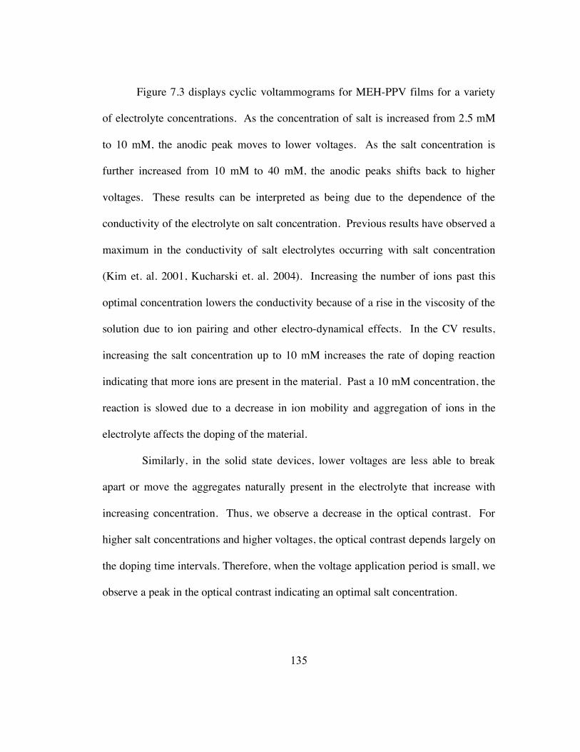
135
Figure 7.3 displays cyclic voltammograms for MEH-PPV films for a variety
of electrolyte concentrations. As the concentration of salt is increased from 2.5 mM
to 10 mM, the anodic peak moves to lower voltages. As the salt concentration is
further increased from 10 mM to 40 mM, the anodic peaks shifts back to higher
voltages. These results can be interpreted as being due to the dependence of the
conductivity of the electrolyte on salt concentration. Previous results have observed a
maximum in the conductivity of salt electrolytes occurring with salt concentration
(Kim et. al. 2001, Kucharski et. al. 2004). Increasing the number of ions past this
optimal concentration lowers the conductivity because of a rise in the viscosity of the
solution due to ion pairing and other electro-dynamical effects. In the CV results,
increasing the salt concentration up to 10 mM increases the rate of doping reaction
indicating that more ions are present in the material. Past a 10 mM concentration, the
reaction is slowed due to a decrease in ion mobility and aggregation of ions in the
electrolyte affects the doping of the material.
Similarly, in the solid state devices, lower voltages are less able to break
apart or move the aggregates naturally present in the electrolyte that increase with
increasing concentration. Thus, we observe a decrease in the optical contrast. For
higher salt concentrations and higher voltages, the optical contrast depends largely on
the doping time intervals. Therefore, when the voltage application period is small, we
observe a peak in the optical contrast indicating an optimal salt concentration.
136
Figure 7.3 Cyclic voltammograms normalized at the anodic peak taken at 20
mV/s for varying salt concentrations from 2.5 mM to 40 mM.
7.5 Conclusions
In conclusion, an ECD was constructed from light-emitting polymer MEH-
PPV that exhibited visible change in color and reversible characteristics. The degree
of the voltage-dependent color change is dependent on polymer layer thickness, anion
type, and salt concentration. Visible color change begins at about 1.5V, but a voltage
of about 1.8V is necessary to fully dope the polymer film. Preliminary results suggest
that organic anions result in higher optical contrasts and that the limiting factor in the
dependence of optical contrast on salt concentration is related to the time interval in
which the doping reaction is allowed to take place. These results have implications
for controlling doping in PPV-based polymer LECs, actuators, and sensors.

137
CHAPTER 8
REVERSIBLE THERMOCHROMIC EFFECTS IN MEH-PPV
8.1 Abstract
We study the thermochromic response of MEH-PPV thin films. MEH-PPV
undergoes a reversible, continuous color change from red to yellow in the practically
relevant temperature range of 25 °C – 100 °C. We show that the absorption of MEH-
PPV continuously decreases and blue-shifts as the temperature is increased. The shift
in HOMO/LUMO levels responsible for the widening of the bandgap was
investigated using temperature dependent cyclic voltammetry. We find that both the
HOMO and LUMO levels increase with heating. Understanding the changes in the
energetic structure of this widely used, versatile material at elevated temperatures is
important in controlling the operation of such devices as polymer photovoltaics.
8.2 Introduction
Thermochromic materials, or materials that change their color depending on
temperature, have been known for some time (Granqvist 1990). The applications for
such materials include smart windows, temperature sensors, color filters, and
displays. The typical organic thermochromic materials achieve color change with
increased temperature through a change in crystal structure (Crano and Guglielmetti
1999). The discovery that conjugated polymers, which are naturally disordered in the

138
solid state, can also undergo temperature-dependent color changes occurred in 1988
using substituted polythiophenes (Yoshino et. al. 1989). Polymers of this type form
the bulk of the literature on thermochromic effects in conjugated polymers. A few
polyphenylenevinylene (PPV) derivatives that display thermochromic properties have
been reported (Gelinck et. al. 1996, Chen et. al. 1998, Onoda et. al. 2003). However,
these materials suffer from low contrast at practical temperature ranges, low
reversibility, or phase changes that accompany the color change, rendering them
impractical for many applications.
We report a study on the thermochromic effects in the widely used light-
emitting polymer MEH-PPV. Thin gel films of MEH-PPV were formed that
exhibited a striking color change from red to yellow when heated from room
temperature to 100C. The color change was rapid, reversible, and was not
accompanied by any phase or volume changes. We measured the temperature-
dependent absorption spectra of these films and showed that a temperature increase
results in a continuous blue-shift and decrease in spectral weight of the polymer
absorption spectra. We performed temperature-dependent cyclic voltammetry
experiments in order to understand how the HOMO and LUMO levels were shifting
to produce an overall blue-shift in the polymer bandgap. Our results are consistent
with conformational changes in the polymer backbone induced by heating.
139
8.3 Experimental details
The primary thermochromic species studied was MEH-PPV, provided by
American Dye Source. MEH-PPV is an orange-red colored, luminescent polymer
easily solvable in common organic solvents. Thermochromic MEH-PPV gel films
were prepared from a solution of 0.8% MEH-PPV in a mixture of chlorobenzene and
dibutyl sebacate at a typical ratio of 5:1. Similar thermochromic effects were
observed with pure MEH-PPV films but the effects appeared to be slower and slightly
less reversible. The solution is spin-cast on quartz substrates and dried under vacuum
(10-6 Torr) overnight prior to testing. For typical purposes, temperature is controlled
by placing the film on a hot-plate.
Transmission spectra for thermochromic films were taken on an n&k Varian
Cary 3 spectrophotometer. Samples were heated in situ by securing a nichrome wire
against the outer edge of the film with a conductive tape and passing current through
the wire. Heating of the film occurred through conduction and therefore suffered a
minor level of non-uniformity. Temperatures were tested immediately prior to the
scan at the film center. The high-temperature limit of such a setup appeared to be the
breakdown of the tape adhesive occurring at around 80 °C.
Cyclic voltammetry experiments were performed using a non-aqueous
silver/silver ion reference electrode (Ag/Ag+, 0.3 V vs. SCE), a platinum counter
electrode and a spin-cast MEH-PPV/ITO working electrode. Solutions were 1%
MEH-PPV in chlorobenzene. Following polymer deposition, all substrates were

140
annealed at 120 C for 30 minutes under vacuum, and dried in a vacuum chamber
(!10-6 torr) overnight. The electrolyte consisted of 0.01 M tetrabutylammonium
tetrafluoroborate (TBA BF4) in acetonitrile and was purged with nitrogen prior to
testing in order to reduce air contamination. Data was obtained on an EG&G
Princeton Applied Research Model 362 Scanning potentiostat and two 2010 Keithley
mulitmeters. The entire cell was placed on a hot plate and the temperature monitored
by thermometer. Electrolyte was allowed to reach equilibrium temperature prior to
scanning.
8.4 Results and discussion
Figure 8.1 shows photographs of the MEH-PPV films at 25 °C, 62 °C, 80 °C,
and 100 °C. In this temperature range, the film undergoes a transition from a slightly
orange-red to yellow. After placing the film on the hot-plate, the color change
occurred in less than one second. After removing the film from the heat source its
original color returned immediately upon cooling of the film. This color change
appeared to be completely reversible and no volume change or melting of the
polymer film was observed.
To understand more qualitatively the observed color change, temperature-
dependent absorption spectra were obtained. The film absorption for 25 °C, 54 °C,
62 °C, and 80 °C are shown in figure 8.2. Clearly as temperature is increased the film
undergoes a continuous blue-shift and decrease in overall absorption. These results

141
Figure 8.1 MEH-PPV gel films at increasing temperatures.

142
are consistent with the well understood proposed mechanism for thermochromic
effects in conjugated polymers first proposed in 1989 (Yoshino 1989). In this model,
the polymer sidechains become bulkier with heating. Stearic hinderance between in-
plane sidechains forces twisting to occur in the polymer backbone. It is this
conformational change in the polymer backbone that shortens the conjugation length
and thus blue-shifts the material absorption (Yoshino et. al. 1989, Garreau et. al.
2003).
Figure 8.2 Temperature-dependent absorption spectra for MEH-PPV.

143
Along with an increase in the polymer effective bandgap, we expect to see
shifting of HOMO/LUMO energy levels. We therefore performed temperature
dependent cyclic voltammetry experiments in the range 25 °C to 40 °C as described
above. HOMO and LUMO levels were extracted from the p and n onset potentials as
described in chapter 6 (Holt et. al. submitted). Figure 8.3 shows the effect of
increased temperature on the HOMO/LUMO levels of MEH-PPV. Both the HOMO
and LUMO levels are increased as the sample is heated, but the LUMO shifts more
dramatically resulting in an overall increase in the bandgap, consistent with the
results obtained for similar PPVs (Onoda et. al. 2003).
Figure 8.3 Temperature dependence of HOMO/LUMO energy levels in MEH-
PPV.

144
8.5 Conclusions
We have studied the thermochromic effects in films of the light-emitting
polymer MEH-PPV. Films exhibited a striking color change from red to yellow when
heated from room temperature to 100 °C. We showed that these films show
promising thermochromic characteristics such as a rapid and reversible color change
in a practical temperature range, and that the color change was not accompanied by
any phase or volume changes. We showed that heating results in a continuous blue-
shift and overall decrease in the polymer absorption spectra. We showed that both
the HOMO and LUMO levels are shifting up with increased temperature at different
rates to affect an overall increase in bandgap energy.
MEH-PPV is widely used in such applications as LEDs (Friend et. al. 1990,
Braun and Heeger 1992) and photovoltaics (Yu et. al. 1994), and has been shown to
be promising also in ECDs (Holt et. al. 2005) as well as some sensing applications
(Chen et. al. 1999). The demonstration of promising thermochromic properties in
such a versatile, robust material introduces the possibility of realizing novel
multifunctional device structures, particularly sensors. Further, an understanding of
how the energetic structure of such materials change with increasing temperature is
crucial for the development of applications such as polymer solar cells, which can be
sensitive to changes in HOMO/LUMO levels and which may require operation at
varying elevated temperatures.

145
BIBLIOGRAPHY
J.J. Apperloo, J. van Haare and R. Janssen, “Transparent highly-oxidized conjugated
polymer films from solution”, Synt. Met. 101, 417 (1999).
M. Ariu, D. G. Lidzey and D. D. C. Bradley, “Influence of film morphology on the
vibrational spectra of dioctyl substituted polyfluorene (PFO)”, Synthetic Metals 607,
111 (2000).
V. I. Arkhipov, P. Heremans, E. V. Emelianova, G. J. Adriaenssens, and H. Bässler,
“Charge carrier mobility in doped semiconducting polymers”, App. Phys. Lett. 82,
3245 (2003).
Ashcroft and Mermin, “Solid state physics”, Saunders College Publishing, (1976).
P.W. Atkins, “Physical chemistry” 4th ed., Oxford University Press (1990).
D. Baeriswyl, D. Campbell and S. Mazumdar, “Conjugated Conducting Polymers”,
edited by H. Kiess (Springer-Verlag, Berlin, 1992), pp. 36-46; H.G. Kiess and G.
Harbeke, ibid., pp. 191-195.
M. Baitoul, J.P. Buisson, S. Lefrant, B. Dulier, J. Wery, and M. Lapkowski,
“Spectroelectrochemical and structural studies of p-doped poly(p-phenylene
vinylene)”, Synt. Met. 84, 623 (1997).
M. Baitoul, J. Wery, J.P. Buisson, G. Arbuckle, H. Shah, S. Lefrant, and M
Hamdoume, “In situ resonant raman and optical investigations of p-doped poly (p-
phenylene vinylene)”, Polymer 44, 6955 (2000).
Bard and Faulkner, “Electrochemical Methods: Fundamentals and Applications”,
Wiley (1980).
F. G. K. Baucke, “Electrochromic mirrors with variable reflectance”, Sol. Energy
Mat. 16 (1987) 67.
G. Björk, S. Machida, Y. Yamamoto, and K. Igeta, “Modification of spontaneous
emission rate in planar dielectric microcavity structures”, Phys. Rev. A 44, 669
(1991).
146
P. W. M. Blom, M. J. M. de Jong, C. T. H. F. Liedenbaum, and J. J. M. Vleggaar,
“Device characteristics of polymer light-emitting diodes”, Synth. Met. 85, 1287
(1997).
P. W. M. Blom and M. J. M. de Jong, “Device operation of polymer light-emitting
diodes”, Philips J. Res. 51, 479 (1998).
L. Bozano, S. A. Carter, J. C. Scott, G. G. Malliaras, and P. J. Brock, “Temperature-
and field-dependent electron and hole mobilities in polymer light-emitting diodes”,
Appl. Phys. Lett. 74, 1132 (1999).
C.J. Brabec, N.S. Sariciftci, and J.C. Hummelen, “Plastic solar cells”, Adv. Funct.
Mater. 11, 15 (2001).
D. D. C. Bradley, G. P. Evans, and R. H. Friend, “Characterisation of
poly(phenylenevinylene) by infrared and optical absorption”, Synth. Met. 17, 651
(1987).
D. Braun and A. J. Heeger, “Visible light emission from semiconducting polymer
diodes”, Appl. Phys. Lett. 58, 1982 (1991).
D. Braun and A.J. Heeger, “Electroluminescence from light-emitting diodes
fabricated from conducting polymers”, Thin Solid Films 216, 96 (1992).
J.L. Bredas, J.C. Scott, K. Yakushi, and G.B. Street, “Polarons and bipolarons in
polypyrrole: Evolution of the band structure and optical spectrum upon doping”,
Phys. Rev. B 30, 1023 (1984).
J.L. Bredas and G.B. Street, “Polarons, bipolarons, and solitons in conducting
polymers”, Acc. Chem. Res. 18, 309 (1985).
V. Bulovic, V. B. Khalfin, G. Gu, and P. E. Burrows, “Weak microcavity effects in
organic light-emitting devices”, Phys. Rev. B 58, 3730 (1998).
S. E. Burns, N. C. Greenham, and R. H. Friend, “Modelling of optical interference
effects in conjugated polymer films and devices”, Synth. Met. 76, 205 (1996).
J.H. Burroughes, C.A. Jones, and R.H. Friend, “New semiconductor device physics in
polymer diodes and transistors”, Nature 335, 137 (1988).

147
J. H. Burroughes, D. D. C. Bradley, A. R. Brown, R. N. Marks, K. Mackay, R. H.
Friend, P. L. Burns, and A. B. Holmes, Light-emitting diodes based on conjugated
polymers”, Nature 347, 539 (1990).
A. J. Campbell, H. Antoniadis, T. Virgili, D. G. Lidzey, X. Wang, and D. D. C.
Bradley, “Balancing electron and hole currents in single layer poly(9,9-
dioctylfluorene) light emitting diodes”, Proceedings of SPIE Vol. 4464 (2002).
H. Campbell, T. W. Hagler, D. L. Smith, and J. P. Ferraris, “Direct Measurement of
conjugated polymer electronic excitation energies using metal/polymer/metal
structures”, Phys. Rev. Lett. 76, 1900 (1996).
Y. Cao, G. Yu, A. J. Heeger, and C. Y. Yang, “Efficient, fast response light-emitting
electrochemical cells: Electroluminescent and solid electrolyte polymers with
interpenetrating network morphology”, Appl. Phys. Lett. 68, 3218 (1996).
S. A. Carter, M. Angelopoulos, S. Karg, P. J. Brock, and J. C. Scott, “Polymeric
anodes for improved polymer light-emitting diode performance”, Appl. Phys. Lett.
70, 2067 (1997).
R. Cervini, X.C. Li, G.W.C. Spencer, A.B. Holmes, S.C. Moratti and R.H. Friend,
“Electrochemical and optical studies of PPV derivatives and poly(aromatic
oxadiazoles)”, Synt. Met. 84, 359 (1997).
V. Cimrova and D. Neher, “Microcavity effects in single-layer light-emitting devices
based on poly(p-phenylene vinylene)”, J. Appl. Phys. 79, 3299 (1996).
L. Chen, D.W. McBranch, H. Wang, R. Helgeson, F. Wudl and D. Whitten, “Highly
sensitive biological and chemical sensors based on reversible fluorescence quenching
in a conjugated polymer”, PNAS 96, 12287 (1999).
S.A. Chen and E.C. Chang, “Structure and properties of cyano-substituted Poly(2,5-
dialkoxy-p-phenylene vinylenes)”, Macromolecules 31, 4899 (1998).
J.C. Crano and R.J. Gugliemetti, “Organic photochromic and thermochromic
compounds”, New York: Plenum Press V.2 1999.
O. H. Crawford, “Radiation from oscillating dipoles embedded in a layered system”,
J. Chem. Phys. 89, 6017 (1988).
P. S. Davids, I. H. Campbell, and D. L. Smith, “Device model for single carrier
organic diodes”, J. Appl. Phys. 82, 6319 (1997).

148
D.M. deLeeuw, M.M.J. Simenon, A.R. Brown, and R.E.F. Einerhand, “Stability of n-
type doped conducting polymers and consequences for polymeric miroelectronic
devices”, Synt, Met. 87, 53 (1997).
J. C. deMello, N. Tessler, S. C. Graham, and R. H. Friend, “Ionic space-charge
effects in polymer light-emitting diodes”, Phys. Rev. B 57, 12951 (1998).
J.C. deMello, J.J.M. Halls, S.C. Graham, N. Tessler, and R.H. Friend, “Electric field
distribution in polymer light-emitting electrochemical cells”, Phys. Rev. Lett. 85, 421
(2000).
M.A. DePaoli, S.Panero, P.Prosperi, and B. Scrosati, “Study of the electrochromism
of polypyrrole/dodecylsulfate in aqueous solutions”, Electrochimica Acta 35, 1145
(1990).
D.J. Dick, A.J. Heeger, Y. Yang, and Q. Pei, “Imaging the structure of the p-n
junction in polymer light-emitting electrochemical cells”, Adv. Mat. 8, 985 (1996).
H. Eckhardt, L. W. Shacklette, K. Y. Jen, and R. L. Elsenbaumer, “The electronic and
electrochemical properties of poly(phenylene vinylenes) and poly(thienelyne
vinylenes): An experimental and theoretical study”, J. Chem. Phys. 91, 1303 (1989).
L. Edman, M.A. Summers, S.K. Burratto, and A.J. Heeger, “Polymer light-emitting
electrochemical cells: Doping, luminescence, and mobility”, Phys. Rev. B 70 (2004).
A. J. Epstein, “Electrically conducting polymers: Science and Technology”, MRS
Bulletin, 16 (1997).
K. Fesser, A.R. Bishop, and D.K. Campbell, “Optical Absorption from polarons in a
model of polyacetylene”, Phys. Rev. B 27, 4804 (1983).
S.R Forrest, “The path to ubiquitous and low-cost organic electronic appliances on
plastic”, Nature 428, 911 (2004).
R. H. Fowler and L. Nordheim, “Electron emission in intense electric fields”, Proc.
Roy. Soc., London, A119, 173 (1928).
R. H. Friend, R. W. Gymer, A. B. Holmes, J. H. Burroughes, R. N. Marks, C. Taliani,
D. D. C. Bradley, D. A. Dos Santos, J. L. Bredas, M. Logdlund and W. R. Salaneck,
“Electroluminescence in conjugated polymers”, Nature 397, 121 (1999).

149
E. Fukada, “History and recent progress on piezoelectric polymers”, IEEE
Transactions on Ultrasonics, Ferroelectrics, and Frequency Control 47, 1277 (2000).
Y. Furukawa, “Electronic Absorption and Vibrational Spectroscopies of Conjugated
Conducting Polymers”, J. Phys. Chem. 100, 15644 (1996).
J. Gao and J. Dane, “Planar light-emitting electrochemical cells with extremely large
interelectrode spacing”, Appl. Phys. Lett. 83, 3027 (2003).
J. Gao and J. Dane, “Visualization of electrochemical doping and light-emitting
junction formation in conjugated polymer films”, Appl. Phys. Lett. 84, 2778 (2004).
F. Garnier, G. Tourillon, M. Gazard, and J. C. Dubois, “Organic conducting polymers
derived from substituted thiophenes as electrochromic material”, J. Electroanal.
Chem. 148 (1983) 299.
S. Garreau, M. Leclerc, N. Errien, and G. Louarn, “Planar-to-nonplanar
conformational transition in thermochromic polythiophenes: A spectroscopic study”,
Macromolecules 36, 692 (2003).
G.H. Gelinck, J.M. Warman, and E.G.J. Staring, “Polaron pair formation, migration,
and decay on photoexcited poly(phenylenevinylene) chains”, J. Phys. Chem. 100,
5485 (1996).
C.G. Granqvist, “Chromogenic materials for transmittance control of large-area
windows”, Critical Reviews in Solid State and Materials Sciences 16, 291 (1990).
S. Hayashi, K. Kaneto and K. Yoshino, “Quenching of photoluminescence in
poly(thiophene) films by electrochemical doping”, Solid State Commun. 61, 249
(1987).
W. Helfrich and W.G. Schneider, “Transients of volume-controlled current and of
recombination radiation in anthracene”. J. Chem. Phys. 44, 2902 (1966).
A.L. Holt, J.M. Leger, and S.A. Carter, “Solid-State electrochromic devices based on
PPV polymers”, APL 86, (2005).
A.L. Holt, J.M. Leger, and S.A. Carter, “Electrochemical and optical characterization
of p- and n-doped MEH-PPV”, (submitted).

150
H. -H. Hörhold, H. Tillmann, C. Bader, R. Stockmann, J. Nowotny, E. Klemm, W.
Holzer, and A. Penzkofer, “MEH-PPV and dialkoxy phenylene vinylene copolymers.
Synthesis and lasing characterization”, Synth. Met. 119, 199 (2001).
A.L. Holt, J.M. Leger and S.A. Carter, “Solid-state electrochromic devices based on
poly(phenylenevinylene polymers”, Appl. Phys. Lett. 68, (2005).
D.M. Ivory, G.G. Miller, J.M. Sowa, L.W. Shacklette, R.R. Chance, and R.H.
Baughman, “Highly conducting charge-transfer complexes of poly(p-phenylene)”, J.
Chem. Phys. 71, 1506 (1979).
R. Jakubiak, C. J. Collison, W. C. Wan, L. J. Rothberg, and B. R. Hsieh, “Reduction
of photoluminescence quantum yield by interchain interactions in conjugated polymer
films”, J. Chem. Phys. A 103, 2394 (1999).
S. Janietz, D. D. C. Bradley, M. Grell, C. Giebeler, M. Inbasekran, and E. P. Woo,
“Electrochemical determination of the ionization potential and electron affinity of
poly(9,9-dioctylfluorene)”, Appl. Phys. Lett. 73, 2453 (1998).
S.A. Jenekhe and J.A. Osaheni, “Excimers aned exciplexes of conjugated polymers”,
Science 265, 765 (1994).
J. Kagan, “Organic photochemistry: Principles and applications”, Academic Press
(1993).
J. -S. Kim, P. K. H. Ho, N. C. Greenham, and R. H. Friend, “Electroluminescence
emission pattern of organic light-emitting diodes: Implications for device efficiency
calculations”, J. Appl. Phys. 88, 1073 (2000).
S. H. Kim, J. K. Choi, and Y. C. Bae, “Mechanical properties and ionic conductivity
of gel polymer electrolyte based on poly(vinylidene-fluoride-co-
hexafluoropropylene)”, J. App. Polymer Science 81, 948 (2001).
T. Kobayashi, H. Yoneyama, and H. Tamura, “Polyanaline film-coated electrodes as
electrochromic display devices”, J. Electroanal. Chem. 161 (1984) 419.
M. Kucharski, T. Lukazewicz, and P. Morozek, Opto-Electron. Rev., 12, 175 (2004).
P. Langevin, Annals of Chemical Physics 28, 229 (1903).
T. Lee, H. Lee, and O. Park, “High-efficiency polymer light-emitting devices using
organic salts: A multilayer structure to improve light-emitting electrochemical cells”,
App. Phys. Lett. 81, 214 (2002).

151
S. Lefrant, E. Perrin, J. P. Buisson, H. Eckhardt, and C. C. Han, “Vibrational studies
of polyparaphenylene-vinylene (PPV)”, Synth. Met. 29, E91 (1989).
J. Lekner, "Theory of Reflection", Dodrecht, Nijhoff, 1987.
J.M. Leger, B. Ruhstaller, H.G. Nothofer, U. Scherf, H. Tillman, H.H. Horhold, and
S.A. Carter, “Thickness-dependent changes in the optical properties of PPV- and PF-
based polymer light emitting diodes”, Phys. Rev. B 68, (2003).
J.M. Leger, B. Ruhstaller, and S.A. Carter, “Recomination profiles in MEH-PPV
light-emitting electrochemical cells”, submitted (2005).
S. Li, F. Xiong, H. Zhang, X. Lu, L Yi, and G. Yang, “Fluorescence Quenching of
Poly[2-methoxy-5-(2'-ethylhexoxy)-p-phenylene vinylene] (MEH-PPV) in
Solutions”, Chinese J. Chem. 22, 80 (2004).
Y. Li, Y. Cao, J. Gao, D. Wang, G. Yu, and A. J. Heeger, “Electrochemical
properties of luminescent polymers and polymer light-emitting electrochemical
cells”, Synth. Met. 99, 243 (1999).
W. Lu, A.G. Fadeev, B. Qi, E. Smela, B.R. Mattes, J. Ding, G.M. Spinks, J.
Mazurkiewicz, D. Zhou, G.G. Wallace, D.R. MacFarlane, S.A. Forsyth, and M.
Forsyth, “Use of ionic liquids for !-conjugated polymer electrochemical devices”,
Science 297, 983 (2002).
W. Lukosz, “Light emission by multiple sources in thin layers”, J. Opt. Soc. Am. 71,
744 (1981).
A.G. MacDiarmid and W. Zheng, “Electrochemistry of conjugated polymers and
electrochemical applications”, MRS Bulletin June 1997.
G. G. Malliaras and J. C. Scott, “The roles of injection and mobility in organic light
emitting diodes”, J. Appl. Phys. 83, 5399 (1998).
M. Mastrogostino and L. Soddu, “Electrochemical characterization of ‘n’ doped
polyheterocyclic conducting polymers – I. Polybithiophene”, Electrochim. Acta 35,
463 (1990).
T. Miteva, A. Meisel, W. Knoll, H. G. Nothofer, U. Scherf, D. C. Müller, K.
Meerholz, A. Yasuda, and D. Neher, “Improving the performance of polyfluorene-
based organic light-emitting diodes via end-capping”, Adv. Mat. 13, 565 (2001).

152
P.M.S. Monk, R.J. Mortimer, D.R. Rosseinsky, “Electrochromism: Fundamentals
and Applications”, (VCH Inc, Weinheim, 1995).
D. Monroe, “Hopping in exponential band tails”, Phys. Rev. Lett. 54, 146 (1985).
R. J. Mortimer, “Organic electrochromic materials”, Electrochimica Acta 44, 2971
(1999).
Y. K. Nakazawa, S. A. Carter, H. -G. Nothofer, U. Scherf, V. Y. Lee, R. D. Miller,
and J. C. Scott, “Effects of polymer side-branching in double and single-layer
polyfluorene light-emitting diodes”, Appl. Phys. Lett. 80, 3832 (2002).
K. A. Neyts, “Simulation of light emission from thin-film microcavities”, J. Opt. Soc.
Am. A 15, 962 (1998).
T.-Q. Nguyen, V. Doan, and B. J. Schwartz, “Conjugated polymer aggregates in
solution: Control of interchain interactions”, J. Chem. Phys. 110, 4068 (1999).
P.J. Nigrey, A.G. MacDiarmid, and A.J. Heeger, “Electrochemistry of polyacetylene,
(CH)x: Electrochemical doping of (CH)x films to the metallic state”, JCS Chem.
Comm. 594 (1979).
H. G. Nothofer, Ph.D. Thesis, University of Potsdam, Potsdam, Germany.
J. Obrzut and F.E. Karasz, “Defects in the electronic structure of poly (p-phenylene
vinylene): Electronic spectra, electrochemical behavior, and molecular orbital
calculations”, J. Chem. Phys. 87, 6178 (1987).
M. Onoda and K. Tada, “A consideration of thermochromic behavior in poly(p-
phenylene vinylene derivatives”, Thin Solid Films 438, 187 (2003).
I. Orion, J. P. Buisson, and S. Lefrant, “Spectroscopic studies of polaronic and
bipolaronic species in n-doped poly(paraphenylenevinylene)”, Phys. Rev. B 57, 7050
(1998).
D. Parker, “Carrier tunneling and device characteristics in polymer light-emitting
diodes”, J. Appl. Phys. 75, 1656 (1994).
A.O. Patil, A.J. Heeger, and F. Wudl, “Optical properties of conducting polymers”,
Chem. Rev. 88, 183 (1988).

153
Q. Pei, Y. Yang, G. Yu, C. Zhang, and A. J. Heeger, “Polymer light-emitting
electrochemical cells: In situ formation of a light-emitting p-n junction”, J. Am.
Chem. Soc. 118, 3922 (1996).
Q. Pei, G. Yu, C. Zhang, Y. Yang, and A. J. Heeger, “Polymer light-emitting
electrochemical cells”, Science 269, 1086 (1995).
L. A. A. Pettersson, F. Carlsson, O. Inganas and H. Arwin,
“Spectroscopic ellipsometry studies of the optical properties of doped poly(3,4-
ethelynedioxythiophene): an anisotropic metal”, Thin Solid Films 313, 356 (1998).
J. R. Platt, “Electrochromism, a possible change of color producible in dyes by an
electric field”, J. Chem. Phys. 34 (1961) 862.
I. Riess and D. Cahen, “Analysis of light emitting polymer electrochemical cells”, J.
Appl. Phys. 82, 3147 (1997).
M. Reufer, M.J. Walter, P.G. Lagoudakis, A.B. Hummel, J.S. Kolb, H.G. Roskos, U.
Scherf, and J.M. Lupton, “Spin-conserving carrier recombination in conjugated
polymers”, Nature Materials 4, 340 (2005).
K.K. Rohatgi-Mukherjee, “Fundamentals of Photochemistry”, Wiley Eastern Limited
(1978).
S. Roth, “One-dimensional metals: Conjugated polymers, organic crystals, carbon
nanotubes”, Wiley-VCH (1995).
N.S. Sariciftci, “Primary photoexcitations in conjugated polymers: Molecular
excitation versus semiconductor band model”, World Scientific (1997).
A. Sakamoto, Y. Furukawa, and M. Tasumi, “Resonance Raman and Ultraviolet to
Infrared Absorption Studies of Positive Polarons and Bipolarons in Sulfuric-Acid-
Treated Poly(p-phenylenevinylene)”, J. Phys. Chem. 98, 4635 (1994).
L.F. Santos, L.M. Carvalho, F.E.G. Guimaraes, D. Goncalves and R.M. Faria,
“Electrical and optical properties of light emitting electrochemical cells using MEH-
PPV/PEO:lithium-salt blends”, Synth. Met. 121, 1697 (2001).
L. F. W. Santos, L. Gaffo, L. M. De Carvalho, D. Goncalves, and R. M. Faria,
“Reversible electrochromical response of thin MEH-PPV films”, Mol. Liq. Crys. 374,
469 (2002).

154
Y. Shimoi and S. Abe, “Competition between polarons and bipolarons in
nondegenerate conjugated polymers”, Phys. Rev. B 50, 14781 (1994).
H. Shirakawa, E.J. Louis, A.G. Macdiarmid, C.K. Chiang, and A.J. Heeger,
“Synthesis of electrically conducting organic polymers: Halogen derivatives of
polyacetylene, (CH)x”, JCS Chem. Comm. 578 (1977).
D. L. Smith, “Steady state model for polymer light-emitting electrochemical cells”, J.
Appl. Phys. 81, 2869 (1997).
W.P. Su, J.R. Schrieffer, and A.J. Heeger, “Solitons in polyacetylene”, Phys. Rev.
Lett. 42, 1698 (1979).
W.P. Su, J.R. Schrieffer, and A.J. Heeger, “Soliton excitations in polyacetylene”,
Phys. Rev. B 22, 2209 (1980).
C.W. Tang, “Two-layer organic photovoltaic cell”, Appl. Phys. Lett. 48, 184 (1986).
B. Tian, G. Zerbi, and K. Müllen, “Electronic and structural properties of
polyparaphenylenevinylene from the vibrational spectra”, J. Chem. Phys. 95, 3198
(1991).
B. Thompson, P. Schottland, K. Zong, and J Reynolds, “In situ colorimetric analysis
of electrochromic polymers and devices”, Chem. Mater. 12, 1563 (2000).
M. Tzolov, V. P. Koch, W. Bruetting, and M. Schwoerer, “Optical characterization of
chemically doped thin films of poly(p-phenylene vinylene)”, Synt. Met. 109, 85
(2000).
D. Vanden Bout, W. Yip, D. Hu, D. Fu, T. Swager and P. Barbara, “Discrete intensity
jumps and intramolecular electronic energy transfer in the spectroscopy of single
conjugated polymer molecules”, Science 277, 1074 (1997).
K.F. Voss, C.M. Foster, L. Smilowitz, D. Mihailovic, S. Askari, G. Srdanov, Z. Ni, S.
Shi, A. J. Heeger, and F. Wudl, “Substitution effects on bipolarons in alkoxy
derivatives of poly(1,4-phenylene-vinylene)”, Phys. Rev. B, 43, 5109 (1991).
W. M. V. Wan, N. C. Greenham, and R. H. Friend, “Interference effects in
anisotropic optoelectronic devices”, J. Appl. Phys. 87, 2542 (2000).

155
F. P. Wenzl, P. Pachler, E. J. W. List, D. Somitsch, P. Knoll, S. Patil, R. Guentner, U.
Scherf, and G. Leising, “Self-absorption effects in a LEC with low Stokes shift”,
Physica E 13, 1251 (2002).
E. Werner, M. Meier, J. Gmeiner, M. Herold, W. Brutting, and M. Schwoerer,
“Doping and trap states in PPV light-emitting devices”, Optical Mater. 9, 109 (1998).
M. Yan, L.J. Rothberg, F. Papadimitrakopoulos, M.E. Galvin, and T.M. Miller,
“Defect Quenching of Conjugated Polymer Luminescence”, Phys. Rev. Lett. 73, 744
(1994).
Y. Yang and Q. Pei, “Voltage controlled two color light-emitting electrochemical
cells”, Appl. Phys. Lett. 68, 2708 (1996).
K. Yoshino, S. Nakajima, D.H. Park, and R. Sugimoto, “Thermochromism,
photochromism and anomalous temperature-dependence of luminescence in poly (3-
alkylthiophene) film” , Japanese Journal of Applied Physics 27, L716 (1988).
K. Yoshino, Y. Manda, K. Sawada, M. Onoda, and R. Sugimoto, “Anomalous
dependence of luminescence of poly(3-alkylthiophene) on temperature and alkyl
chain length”, Solid State Commun. 69, 143 (1989).
G. Yu, K. Pakbaz, and A.J. Heeger, “Semiconducting polymer diodes: Large size,
low cost photodetectors with excellent visible-ultraviolet sensitivity”, Appl. Phys.
Lett. 64, 3422 (1994).
G. Yu, C. Zhang, and A.J. Heeger, “Dual-function semiconducting polymer devices:
Light-emitting and photodetecting diodes”, Appl. Phys. Lett. 64, 1540 (1994).
G. Zotti, G. Schiavon and S. Zecchin, “Irreversible processes in the electrochemical
reduction of polythiophenes. Chemical modifications of the polymer and charge-
trapping phenomena”, Synt. Met. 72, 275 (1995).