Embed Size (px)
Citation preview
Physics 156: Applications of Solid State Physics
• Instructor: Sue Carter
• Office NSII 349
• Office Hours: Wednesdays 11:30 to 1 pm or by appointment
• Email: [email protected]
• Book: http://ece-www.colorado.edu/~bart/book/book/title.htm
plus Additional Handouts provided in class
• Homework (30%), Exams (30%), Final Presentation (30%), Class
Participation (10%)
• Applications:
Transistors (MOS, MOSFET,PN junction, Bipolar), Memory, LEDs/LASERs,
Solid State Lighting, Displays, Solar Cells and Photodetectors, Magnetic
Storage, MEMs, Other?
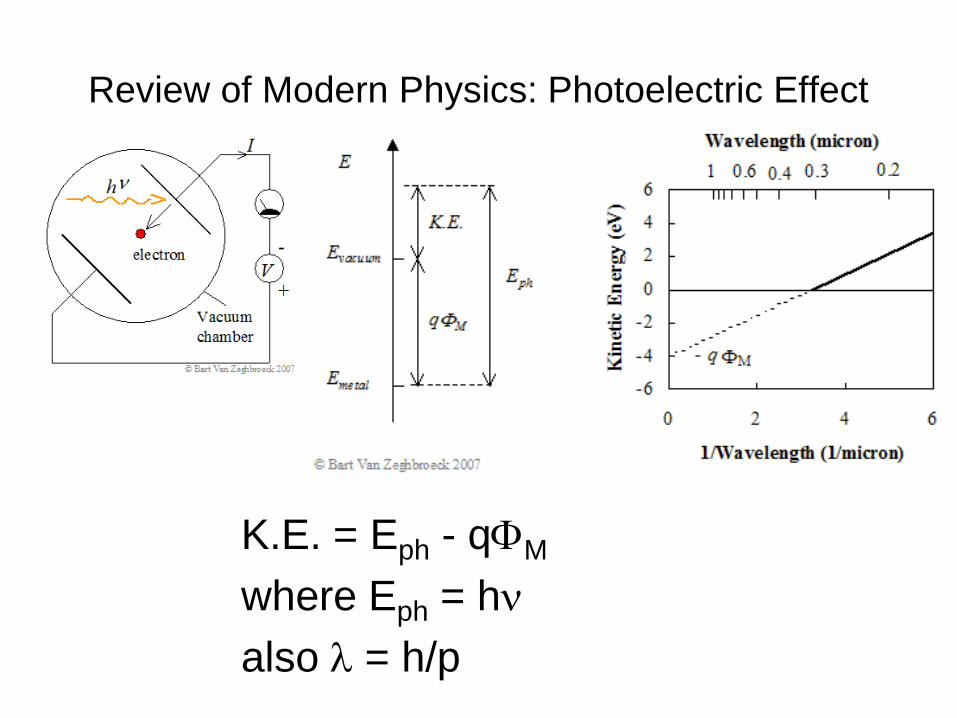
Review of Modern Physics: Photoelectric Effect
K.E. = Eph - qM
where Eph = h
also = h/p
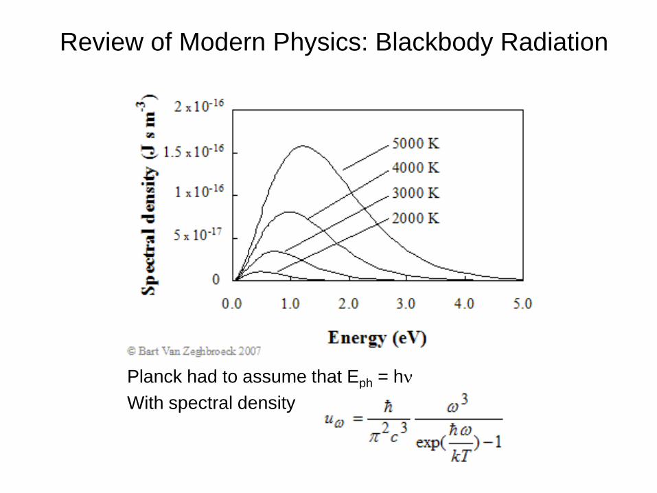
Review of Modern Physics: Blackbody Radiation
Planck had to assume that Eph = h
With spectral density
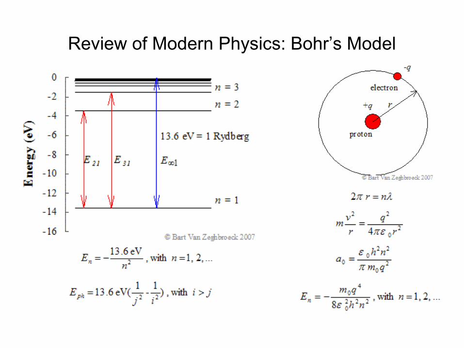
Review of Modern Physics: Bohr’s Model
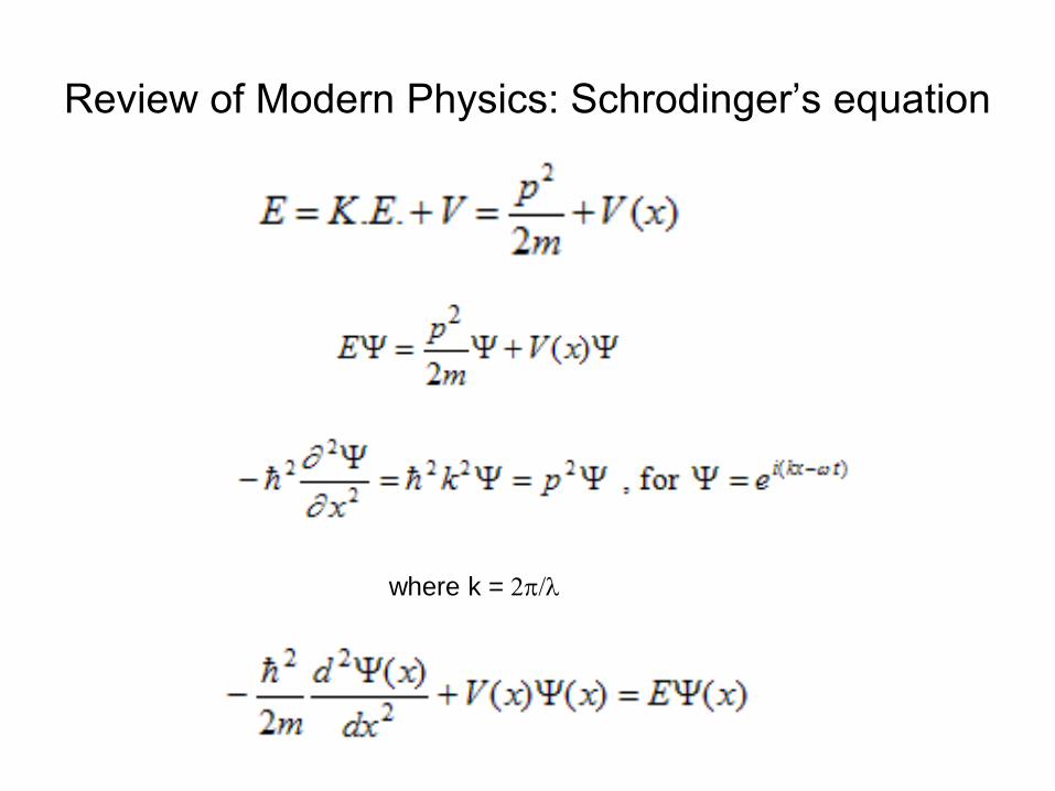
Review of Modern Physics: Schrodinger’s equation
where k = 2/
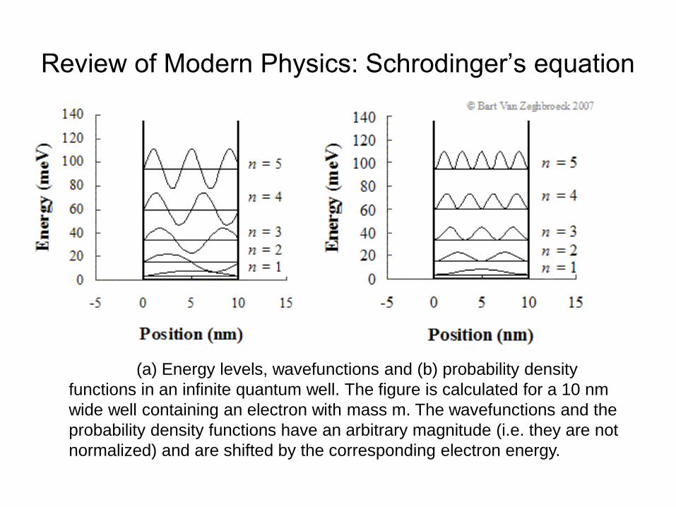
Review of Modern Physics: Schrodinger’s equation
(a) Energy levels, wavefunctions and (b) probability density
functions in an infinite quantum well. The figure is calculated for a 10 nm
wide well containing an electron with mass m. The wavefunctions and the
probability density functions have an arbitrary magnitude (i.e. they are not
normalized) and are shifted by the corresponding electron energy.
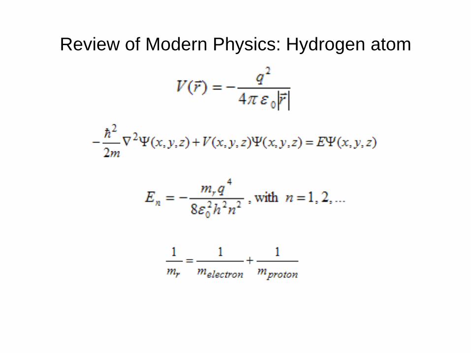
Review of Modern Physics: Hydrogen atom
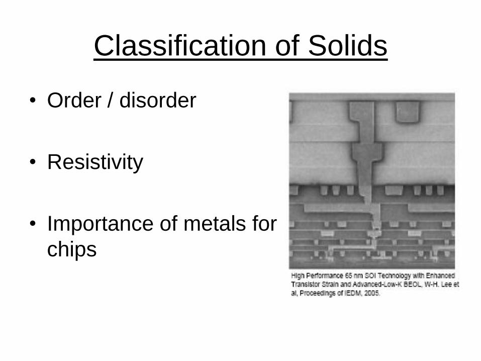
Classification of Solids
• Order / disorder
• Resistivity
• Importance of metals for
chips
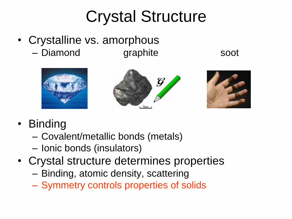
Crystal Structure
• Crystalline vs. amorphous– Diamond graphite soot
• Binding– Covalent/metallic bonds (metals)
– Ionic bonds (insulators)
• Crystal structure determines properties– Binding, atomic density, scattering
– Symmetry controls properties of solids
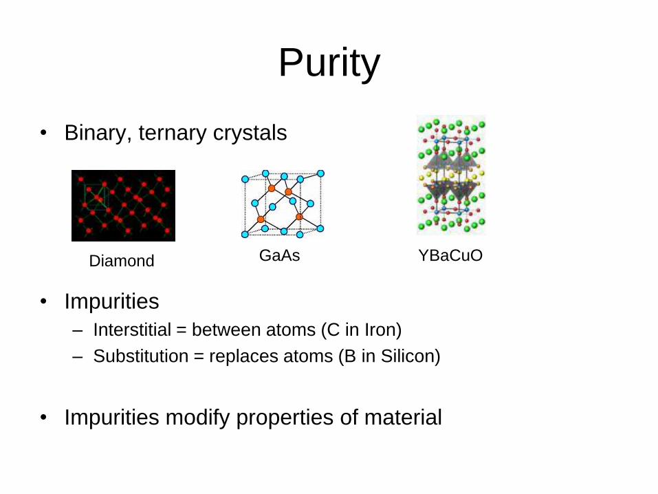
Purity
• Binary, ternary crystals
• Impurities
– Interstitial = between atoms (C in Iron)
– Substitution = replaces atoms (B in Silicon)
• Impurities modify properties of material
GaAsDiamond YBaCuO
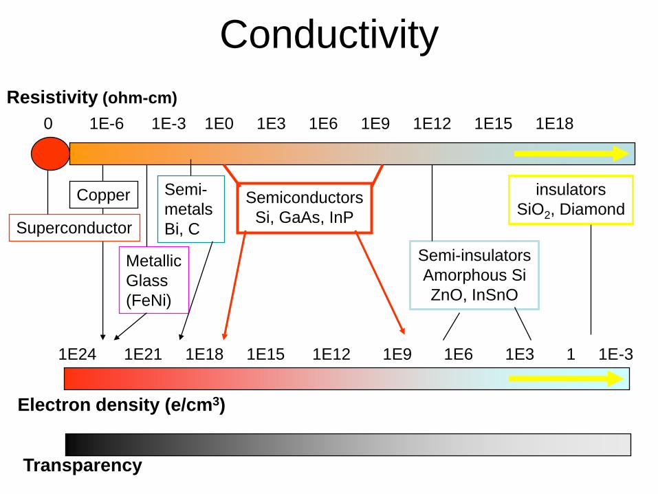
Conductivity
Resistivity (ohm-cm)
0 1E-6 1E-3 1E0 1E3 1E6 1E9 1E12 1E15 1E18
Superconductor
Copper
Metallic
Glass
(FeNi)
Semi-
metals
Bi, C
Semiconductors
Si, GaAs, InP
Semi-insulators
Amorphous Si
ZnO, InSnO
insulators
SiO2, Diamond
1E24 1E21 1E18 1E15 1E12 1E9 1E6 1E3 1 1E-3
Transparency
Electron density (e/cm3)
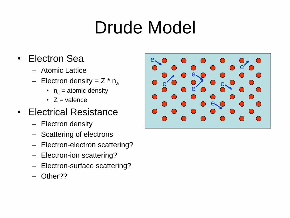
Drude Model
• Electron Sea– Atomic Lattice
– Electron density = Z * na
• na = atomic density
• Z = valence
• Electrical Resistance– Electron density
– Scattering of electrons
– Electron-electron scattering?
– Electron-ion scattering?
– Electron-surface scattering?
– Other??
e
e
e
e
e
e
e
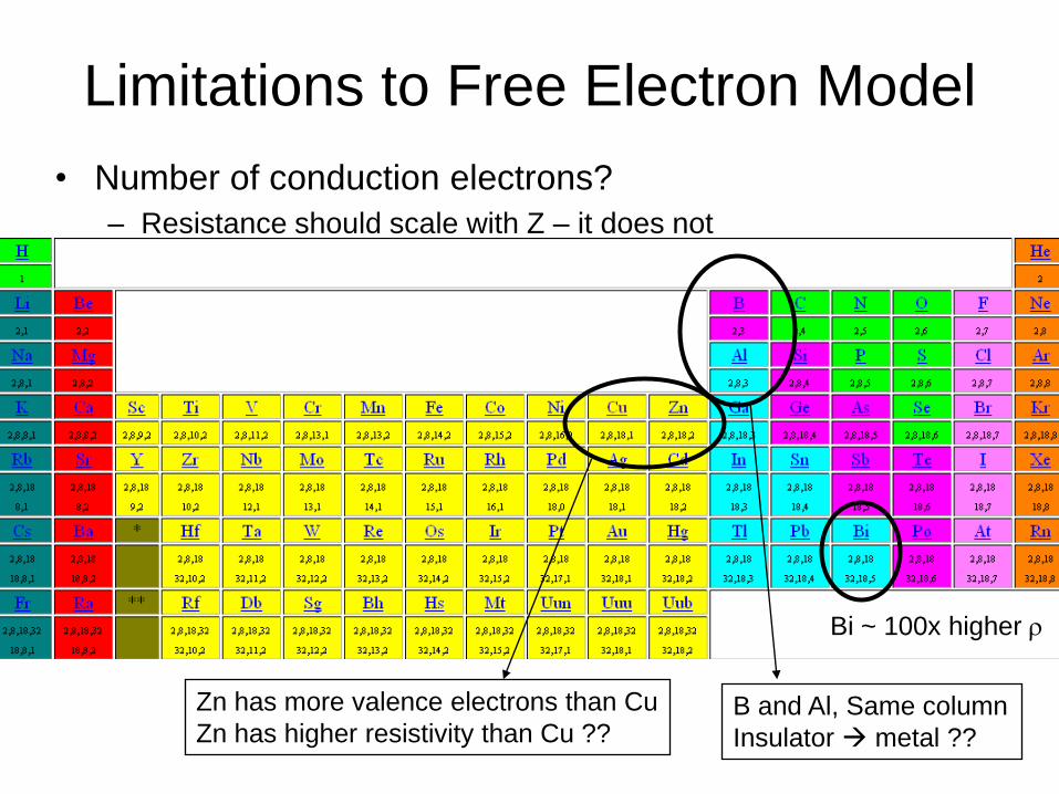
Limitations to Free Electron Model
• Number of conduction electrons?
– Resistance should scale with Z – it does not
B and Al, Same column
Insulator metal ??
Zn has more valence electrons than Cu
Zn has higher resistivity than Cu ??
Bi ~ 100x higher r
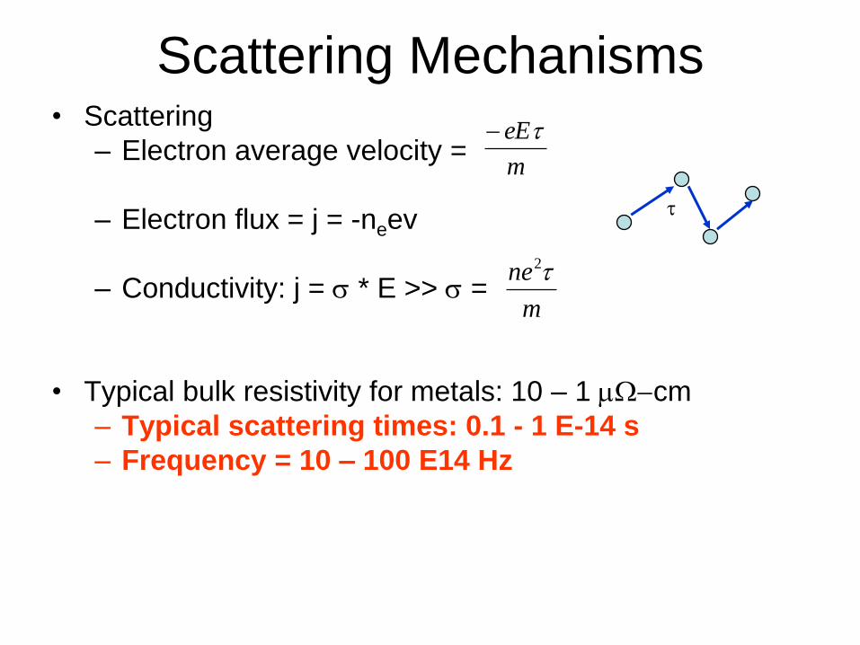
Scattering Mechanisms• Scattering
– Electron average velocity =
– Electron flux = j = -neev
– Conductivity: j = * E >> =
• Typical bulk resistivity for metals: 10 – 1 cm
– Typical scattering times: 0.1 - 1 E-14 s
– Frequency = 10 – 100 E14 Hz
m
eE
m
ne 2
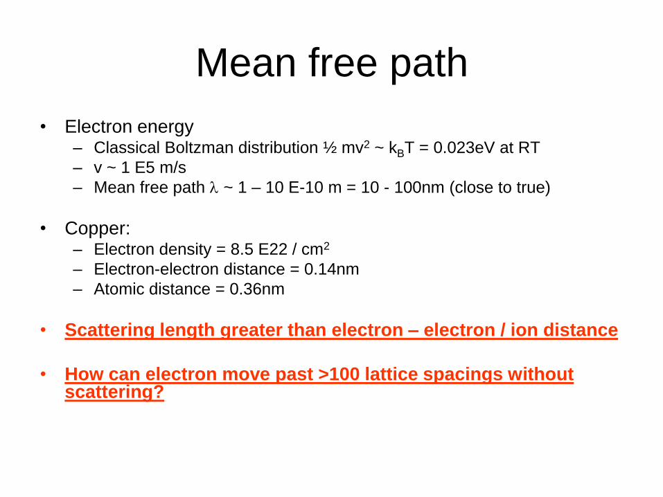
Mean free path
• Electron energy– Classical Boltzman distribution ½ mv2 ~ kBT = 0.023eV at RT
– v ~ 1 E5 m/s
– Mean free path ~ 1 – 10 E-10 m = 10 - 100nm (close to true)
• Copper:– Electron density = 8.5 E22 / cm2
– Electron-electron distance = 0.14nm
– Atomic distance = 0.36nm
• Scattering length greater than electron – electron / ion distance
• How can electron move past >100 lattice spacings without scattering?
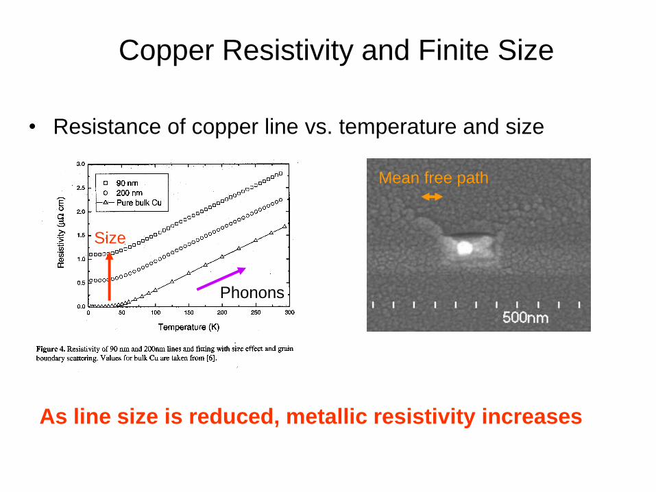
Copper Resistivity and Finite Size
• Resistance of copper line vs. temperature and size
Phonons
Size
As line size is reduced, metallic resistivity increases
Mean free path
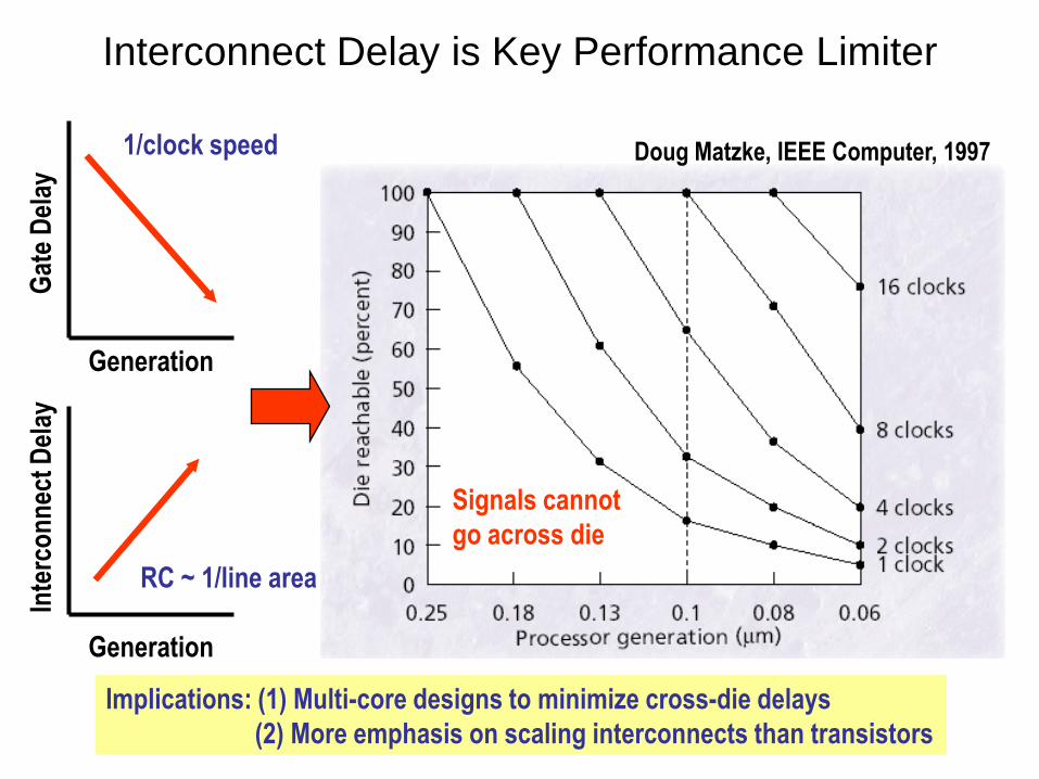
Interconnect Delay is Key Performance Limiter
Generation
Gat
e D
elay
Generation
Inte
rco
nn
ect
Del
ay
1/clock speed
RC ~ 1/line area
Doug Matzke, IEEE Computer, 1997
Implications: (1) Multi-core designs to minimize cross-die delays
(2) More emphasis on scaling interconnects than transistors
Signals cannot
go across die
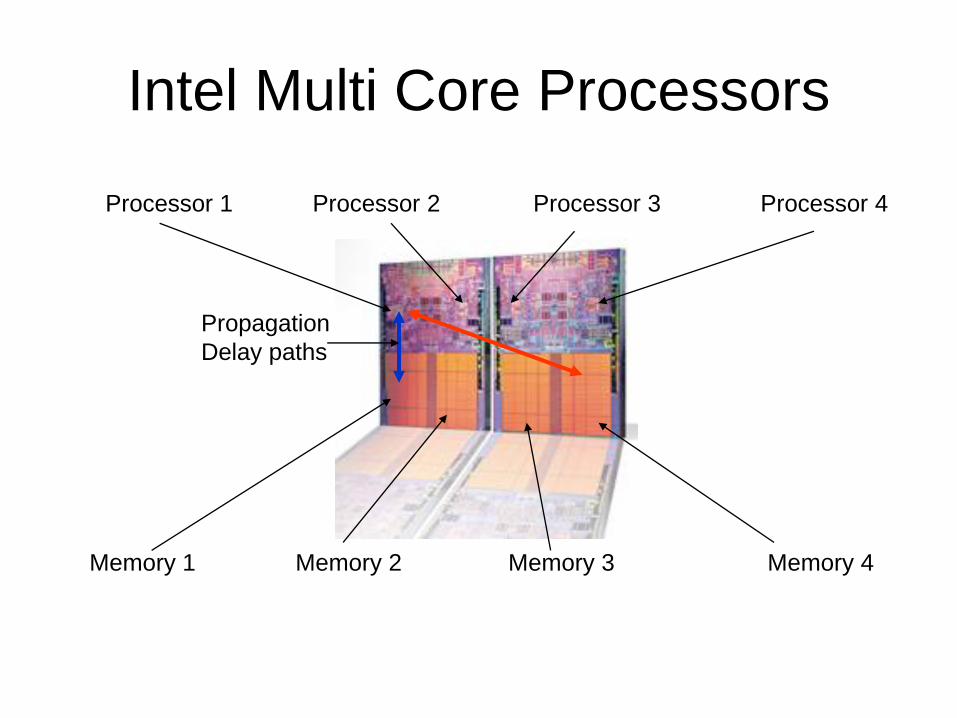
Intel Multi Core Processors
Processor 1 Processor 2 Processor 3 Processor 4
Memory 1 Memory 2 Memory 3 Memory 4
Propagation
Delay paths
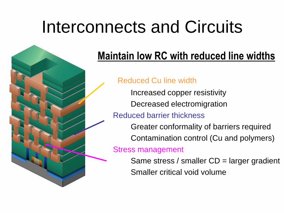
Interconnects and Circuits
Reduced Cu line width
Increased copper resistivity
Decreased electromigration
Reduced barrier thickness
Greater conformality of barriers required
Contamination control (Cu and polymers)
Stress management
Same stress / smaller CD = larger gradient
Smaller critical void volume
Maintain low RC with reduced line widths


![arXiv:1203.6863v1 [math.PR] 30 Mar 2012gerardo/Schroedinger.pdfHITTING TIMES, BRIDGES, AND SCHRODINGER’S EQUATION 5¨ This function h is the hitting time density of Brownian motion](https://img.pdfslide.us/doc/110x75/5f38862f89622b03104d213d/arxiv12036863v1-mathpr-30-mar-gerardoschroedingerpdf-hitting-times-bridges.jpg)