Embed Size (px)
Citation preview
- 1 of 44 -
Interfacing to the Outside World Introduction
There are variety of ways and reasons to talk to outside world Consider first kinds of devices we may want to interface to
For embedded systems tasks include • Measuring • Controlling • Interacting with other subsystems • Computing
Accelerators Graphics
• Communications
Understanding the Problem Background
Study of interaction with external world Examines portions of the von Neumann machine
Designated as Input and Output View hardware and software world outside of the main microprocessor
Through window collectively called the I/O subsystem Devices we may interact with include File systems and storage devices
Read and write data Network
Send and receive data Execute remote procedures
Keyboard and mouse Interact with computer
Scanning devices Bring in information
Display and printing devices Display variety of data
We interact with external devices in several ways
Associated with each input or output device Generally have software procedure called a driver or device driver
Supports interaction with the device Often designated API – application programmer’s interface
When studying input and output interaction with the external world
- 2 of 44 -
Must consider several things • Source or destination for any exchange • I/O ports on the micro processor • Local and global memory address space • Nature of the exchange as event, a shared variable, or a message • I/O procedure invocation and any associated restrictions on procedure • Location of I/O driver • Protocol for the data exchange • Timing requirements • Physical medium of the exchange
Formulating a Model
To understand and manage problem We place external world devices into two general categories
Those that are local Those that are remote
Local Devices
Tend to be in closer proximity to the core system Generally 1 to 3 meters or less
Typically have proprietary or specialized interfaces Any tasks executing on such devices
Usually associated with function of specific device Not considered to be part of the embedded application proper
Interprocess communication and synchronization with such devices Primarily based upon variations on
Shared variable paradigm Simple message exchange
SPI and I2C good examples Interaction with such devices characterized by Local Device Model
Remote Devices Such devices tend to be located at a greater physical distance
3 to 5 meters or more Today with the growth of systems and networks on a chip
Model expands to include external devices On same die or within same gate array
Interaction with remote external devices Begins with notion of distributed tasks executing on these devices
Forms the basis for the Remote Device Model Such tasks often considered to be
- 3 of 44 -
Integral and contributing part of the main application Interprocess communication and synchronization
Typically occurs over a network using message exchange
Formulating a Model - Inside the Microprocessor Begin inside microprocessor as first step to
Formalizing interprocess communication and synchronization Formulate a model based upon three questions What are we communicating? With whom? How do we control the exchange?
These lead to internal model which comprises
• The information Data or signals being moved to convey intent or goals
• Place or places from which information is moved to or from • The control and synchronization of actions and movement of information
With internal model Source and destination for exchange identified by
• Named variables • Pointer variables holding memory addresses
Control and coordination supported by • Flags or status bits to manage and signal
Access to critical areas • Semaphores or monitors
Support more formalized control Formulating a Model - Outside the Microprocessor
Extending model to include interaction with the world Outside of the core processor
Now must expand to include physical means of moving information Interprocess communication model developed earlier
Now must include answer to the question, How do we get the information to where it is going?
Fourth component to the model Becomes the physical means by which the information is moved
The transport mechanism
- 4 of 44 -
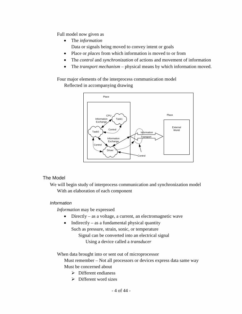
Full model now given as • The information
Data or signals being moved to convey intent or goals • Place or places from which information is moved to or from • The control and synchronization of actions and movement of information • The transport mechanism – physical means by which information moved.
Four major elements of the interprocess communication model
Reflected in accompanying drawing
The Model We will begin study of interprocess communication and synchronization model
With an elaboration of each component
Information Information may be expressed
• Directly – as a voltage, a current, an electromagnetic wave • Indirectly – as a fundamental physical quantity
Such as pressure, strain, sonic, or temperature Signal can be converted into an electrical signal
Using a device called a transducer When data brought into or sent out of microprocessor
Must remember – Not all processors or devices express data same way Must be concerned about Different endianess Different word sizes
CPU
Transport
Information
External World
Driver
Control
Place
Place
Task0
Task1InformationExchange
Control
InformationExchange
Control
- 5 of 44 -
Once inside the microprocessor
These physical quantities are abstracted as • Primitive types such as integers or floats • Complex data types
Collections of primitive types or as structs or classes
Some exchanges will be Unidirectional – either input or output only Bidirectional – (potentially) simultaneous input or output
In collection of applications classed as measurement and control devices
Outgoing information may be Configuration data followed by commands
To execute a measurement or series of measurements To effect a series of control movements
Incoming information returned might be
Results of the measurements Error between commanded and actual control operation
For larger more complex applications
System may be a component in sophisticated networked application May be serving
Video on demand to passengers on commercial airliner Production information around automated manufacturing site
In such cases information most likely expressed in form of messages Exchanged using standard protocol such as TCP/IP or I2C
Places
The source and destination for an exchange May be inside or outside of microprocessor
If extends to locations outside local address space.
Memory location previously reached by dereferencing a pointer May now be several meters away
In device that can only be reached by message exchange Any local address is meaningless
Moving outside of the processor means Managing remote access
- 6 of 44 -
Exchange of information
Source and destination of any exchanges Still identified by addresses
Addresses may be Implicit
Destination device directly connected to output port or bus On the embedded processor
Explicit Source and destination have an associated name
By which they can be referred to by other devices in system Domain name as alias for IP address is example
Communication can be with Single address Subset of all addresses in system All addresses in system
Point to Point
Communication with single address Called point to point
In such cases interaction is with Specific component System Subsystem Other piece of equipment
Exchange may Command a measurement Alter configuration of component Direct it to perform specific operation and return a value Set output to specified value Request status information
Multicast
Communication with reduced subset of system elements Referred to as a multicast
Transfers information only to those for whom it is relevant Entertainment subsystem on a commercial aircraft
If a specific data package to be sent only to first class passengers Broadcast
Communication with all system elements
- 7 of 44 -
Referred to as a broadcast All of the subsystems comprising the application
Broadcast message Used to send the same information to all components Information may direct all member subsystems to
Reset state USB directs all subsystems to disconnect from network
With broadcast message Initiate self-test sequence Signal
State of some system variable has changed Update is necessary
Control and Synchronization
Control and synchronization portion of the model Implemented as combination of both hardware and software
• Hardware portion comprises
Overall structure and organization of transport mechanism Any connected devices Any necessary control signals
• Software component include
Special collection of routines called drivers Used to manage communication with
Individual devices Classes of devices.
Management of remote processes and information exchanges
Is complicated by Intra and inter system delays Failures of the transport mechanism or remote devices themselves
Inside of microprocessor
Shared variables and messages Principal means for executing the information exchange
Outside of microprocessor
Include locations in remote address spaces
- 8 of 44 -
Source or destination of a shared variable pair May include external device
Such as a register or set of registers in peripheral device To which one must write initialization or configuration values
Data buffer on such a device Model must expand to include
Invocation of methods or procedures on remote external devices
Transport The transport mechanism
Physical means by which information moved Can be implemented by any of great variety
Physical mediums and configurations Simple piece of wire Bundle of fiber optic filaments Surrounding air
Target of the exchange can be Local
Within the same gate array Remote – across
Office Factory Country World.
The Copper Connection
Copper is most common and most familiar means of transport today Preference rapidly changing to fiber or air
Basic case transport medium simply Necessary number of wires bundled together Carrying electrical signals from one place to another
Increasing I/O speeds
Beginning to track increasing capabilities of processing units As speed increases
So do fundamental transport difficulties So must quality of communication channel
- 9 of 44 -
Two of main causes of electrical contamination in copper
• Crosstalk between adjacent conducting paths • Noise induced from external sources
Crosstalk
Can be addressed by Alternating signal and ground conductors in conducting path Twisting ground and signals conductors together
External contamination
Can be attacked by Using differential signals Shielding the entire cable or the individual twisted pairs or both
The Fiber Channel
Fiber optics provides an increased level of robustness Prior to transport
Information converted into optical signals That move without electrical interference
Along thin, optically conductive, channels At the end of the day objective remains the same
Reliably move data and control information From one place to another
Today fiber somewhat more expensive than standard copper wire
For most applications In addition to cost of material
Difficulty of making connection with low cost tools
Strength of fiber optics is Immunity to most electrical contamination
That affects traditional wire Both objections will change with time and continued advances in technology.
- 10 of 44 -
The Air Channel Wireless in form of radio waves
Offers another alternative to copper or fiber Wireless communication network
Easy to install Works very well in areas in areas where
Wire infrastructure is not in place Where a temporary connection needed
It’s cheaper and more flexible than a wire based approach However it is typically
Slower than wire More prone to errors from environmental interference
The organization of the transport medium can range
From a few signal lines With information flowing in serial
To a larger number of signals Simultaneously transporting greater amounts of the information
No matter which transport scheme is used Must have solid understanding of
All timing relationships Strengths and limitations of the medium Transport protocol
Exploring the Model
Will now examine each component in model in greater detail Beginning with Transport
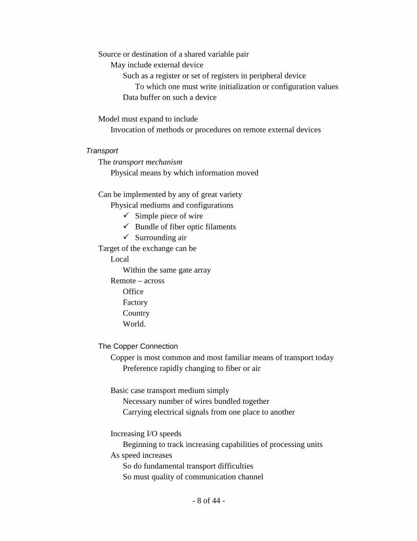
The Transport Mechanism
Hierarchy shown identifies Two major elements of the transport mechanism
Physical level Interconnection architecture
Physical level is means by which information moved
Can be implemented in a variety of ways Interconnection architecture or topology
On top of the physical medium
Physical Level
Architectural Level
- 11 of 44 -
Choice of interconnection topology and architecture Can have a significant effect on performance
In time Reliability Economic cost
The Interconnection Topology
Organizational topology One of important considerations in design of the physical medium
In local device model Medium implements an extension of one of the familiar bus architectures
In the remote device model Medium is more often called a network
Which ever name is used, the intent is the same Among the vast number of ways of configuring the interconnection
Generally one finds three fundamental organizations • Star • Ring • Parallel Bus
Transport mechanism architecture in most contemporary embedded systems Modifies or extends one or more of these in some way
Each configuration has certain advantages and disadvantages As noted earlier
For all configurations there are three kinds of messages • Those addressed to single device (point to point) • To a subset of the devices (multicast) • Those sent to all devices (broadcast)
Each of these configurations can find application in
A (wired) local context Such as a collection of microprocessors in
Contemporary automobile Complex integrated circuit
Remote context Highly distributed wireless or networked system of Internet appliances
- 12 of 44 -
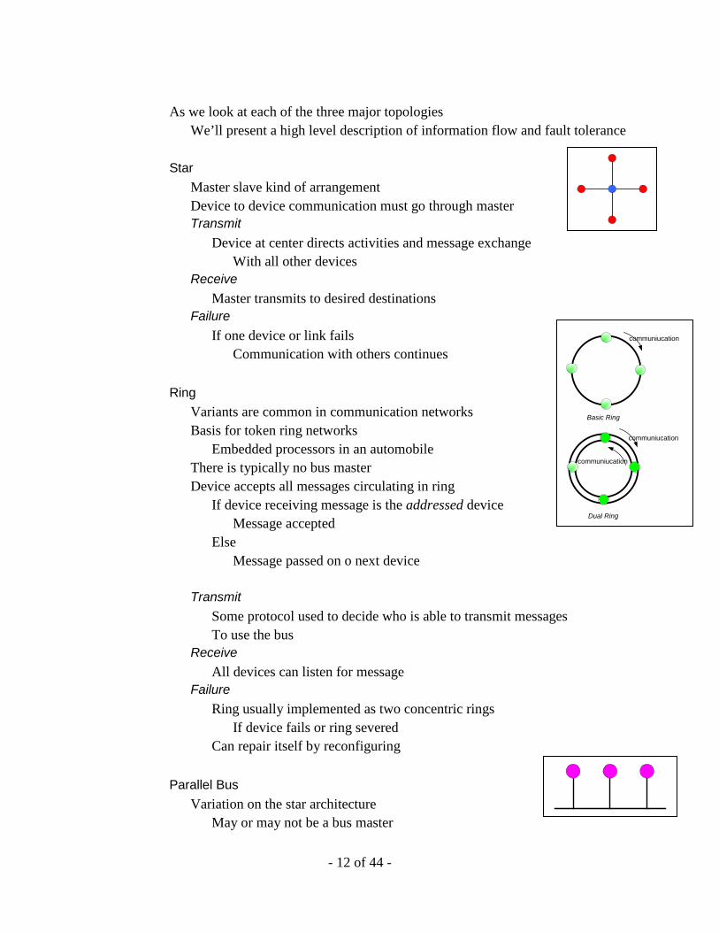
As we look at each of the three major topologies
We’ll present a high level description of information flow and fault tolerance Star
Master slave kind of arrangement Device to device communication must go through master Transmit
Device at center directs activities and message exchange With all other devices
Receive Master transmits to desired destinations
Failure If one device or link fails
Communication with others continues Ring
Variants are common in communication networks Basis for token ring networks
Embedded processors in an automobile There is typically no bus master Device accepts all messages circulating in ring
If device receiving message is the addressed device Message accepted
Else Message passed on o next device
Transmit
Some protocol used to decide who is able to transmit messages To use the bus
Receive All devices can listen for message
Failure Ring usually implemented as two concentric rings
If device fails or ring severed Can repair itself by reconfiguring
Parallel Bus
Variation on the star architecture May or may not be a bus master
communiucation
communiucation
communiucation
Basic Ring
Dual Ring
- 13 of 44 -
Simple bus probably one of more common architectures Device interconnection several ways
All can transmit or receive Some transmit or receive only Control bus to all or request / grant configuration
Transmit
If bus master It addresses device
Sends information Permits another device to transmit
Else Some protocol used to decide who is able to transmit messages To use the bus
Messages may be • Broadcast • Multicast • Polled
Receive
All devices can listen for message and act on message Failure
Individual device failure will not compromise net Severed net can prevent communication beyond severed point
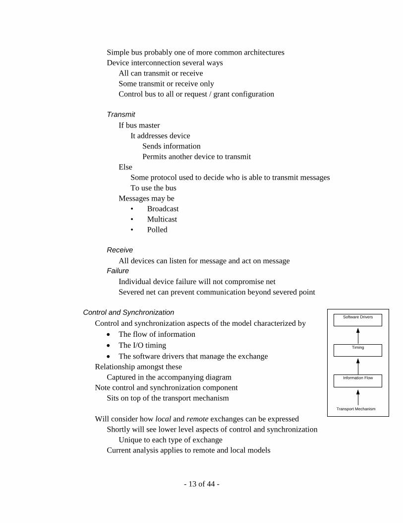
Control and Synchronization
Control and synchronization aspects of the model characterized by • The flow of information • The I/O timing • The software drivers that manage the exchange
Relationship amongst these Captured in the accompanying diagram
Note control and synchronization component Sits on top of the transport mechanism
Will consider how local and remote exchanges can be expressed
Shortly will see lower level aspects of control and synchronization Unique to each type of exchange
Current analysis applies to remote and local models
Information Flow
Timing
Software Drivers
Transport Mechanism
- 14 of 44 -
Information Flow Managing movement of information
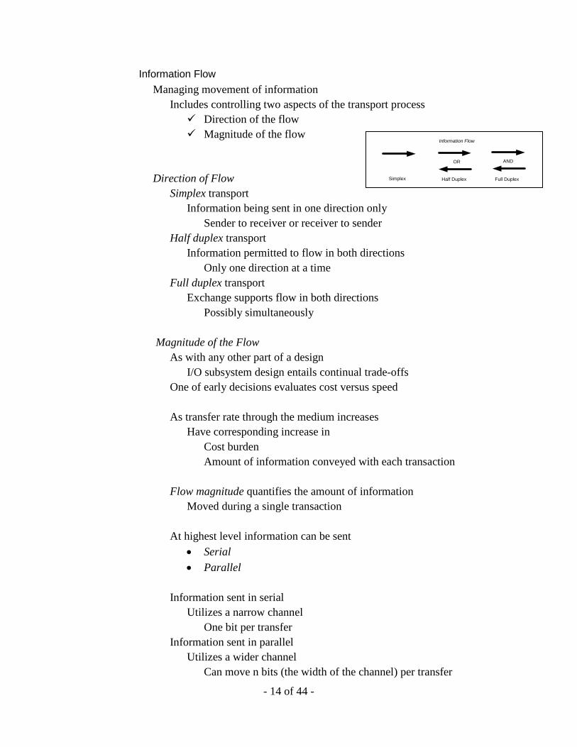
Includes controlling two aspects of the transport process Direction of the flow Magnitude of the flow
Direction of Flow
Simplex transport Information being sent in one direction only
Sender to receiver or receiver to sender Half duplex transport
Information permitted to flow in both directions Only one direction at a time
Full duplex transport Exchange supports flow in both directions
Possibly simultaneously
Magnitude of the Flow As with any other part of a design
I/O subsystem design entails continual trade-offs One of early decisions evaluates cost versus speed As transfer rate through the medium increases
Have corresponding increase in Cost burden Amount of information conveyed with each transaction
Flow magnitude quantifies the amount of information
Moved during a single transaction At highest level information can be sent
• Serial • Parallel
Information sent in serial
Utilizes a narrow channel One bit per transfer
Information sent in parallel Utilizes a wider channel
Can move n bits (the width of the channel) per transfer
Simplex Half Duplex Full Duplex
OR AND
Information Flow
- 15 of 44 -
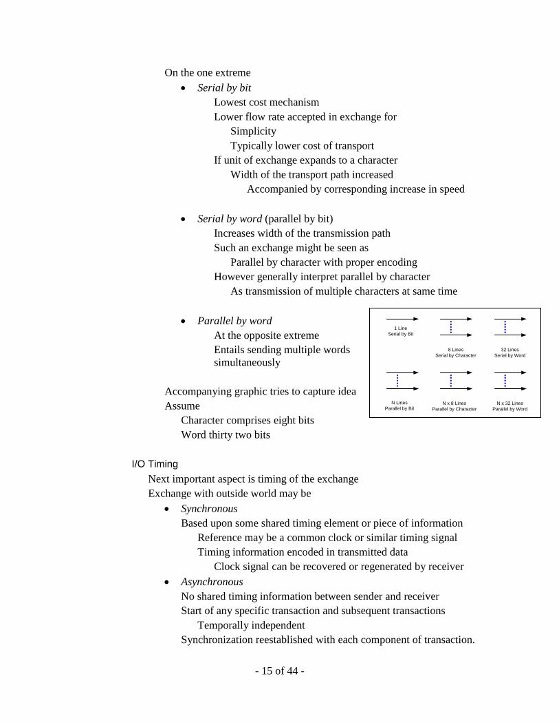
On the one extreme • Serial by bit
Lowest cost mechanism Lower flow rate accepted in exchange for
Simplicity Typically lower cost of transport
If unit of exchange expands to a character Width of the transport path increased
Accompanied by corresponding increase in speed
• Serial by word (parallel by bit) Increases width of the transmission path Such an exchange might be seen as
Parallel by character with proper encoding However generally interpret parallel by character
As transmission of multiple characters at same time
• Parallel by word At the opposite extreme Entails sending multiple words simultaneously
Accompanying graphic tries to capture idea Assume
Character comprises eight bits Word thirty two bits
I/O Timing
Next important aspect is timing of the exchange Exchange with outside world may be
• Synchronous Based upon some shared timing element or piece of information
Reference may be a common clock or similar timing signal Timing information encoded in transmitted data
Clock signal can be recovered or regenerated by receiver • Asynchronous
No shared timing information between sender and receiver Start of any specific transaction and subsequent transactions
Temporally independent Synchronization reestablished with each component of transaction.
1 Line Serial by Bit
8 Lines Serial by Character
32 Lines Serial by Word
N Lines Parallel by Bit
N x 8 Lines Parallel by Character
N x 32 Lines Parallel by Word
- 16 of 44 -
Software Device Drivers – the API Provide significant portion of software side
Of control and synchronization of outside world exchange Sophistication and complexity of these device drivers
Varies greatly with sophistication and complexity of • Embedded design • Devices
Simple washing machine or microwave oven controller Frequently implement control routines as a few function calls
Directly provide and manage Control Data exchange with any hardware
On more powerful systems
Routines provide interface between System software and application tasks Physical devices
Device drivers provide a (common) high level calling interface In support of the I/O operation While separating the users of the devices
From the low level details of managing physical hardware Whether ad hoc or more general purpose
Device driver will typically provide following capabilities Support for registering the device with the system, Device initialization, Support for moving data to and from the device, Support for managing control events such as interrupts.
Device driver may reside in
Main system microprocessor Dedicated peripheral processor.
Independent of
Physical transport architecture Control and synchronization mechanism
Must support remaining two components of the model
Information Places
- 17 of 44 -
Places The places component in the model
At the very minimum identifies the destination of any transfer How information is acquired, represented, and conveyed
Differs between the local devices and the remote devices For local devices
Typically only destination address used For remote devices
Will often include both source and destination address
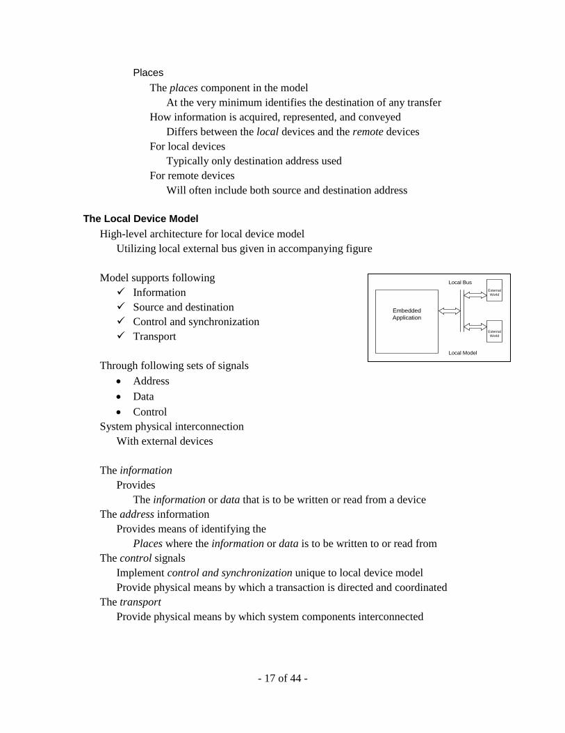
The Local Device Model High-level architecture for local device model
Utilizing local external bus given in accompanying figure
Model supports following Information Source and destination Control and synchronization Transport
Through following sets of signals
• Address • Data • Control
System physical interconnection With external devices
The information Provides
The information or data that is to be written or read from a device The address information
Provides means of identifying the Places where the information or data is to be written to or read from
The control signals Implement control and synchronization unique to local device model Provide physical means by which a transaction is directed and coordinated
The transport Provide physical means by which system components interconnected
Embedded Application
Local Model
External World
External World
Local Bus
- 18 of 44 -
Each of these can be implemented in a variety of ways Depending upon the nature and structure of underlying I/O channel Not unusual for an embedded application to support several different schemes.
Control, Synchronization, and Places
Number and structure of the control signals in a local device model Generally system specific
Typical signals may include • Read / Write signals • Address / Data present or stable strobes • Clock - Where does clock come from
Separate line or encoded in the data • Transmission Direction • Ready or Active • Synchronize • Reset • Power - May or may not be counted as control signal
Means for identifying places involved in exchange must consider
Initial set of devices that make up the system Any new devices that may be added during runtime
If system configuration either never changes or changes infrequently Address assignment can be accomplished using
Set of switches Set of jumpers
As is done on a SCSI device Permanently assigned at the time the device is built
More transient configurations Use geographic addressing
Used by USB With such an approach an address assigned
To every module on bus each time System in powered ON New device attached to system and recognized
Such a process sometimes called enumeration Note that a device may or may not have the same address
Each time system is powered on
- 19 of 44 -
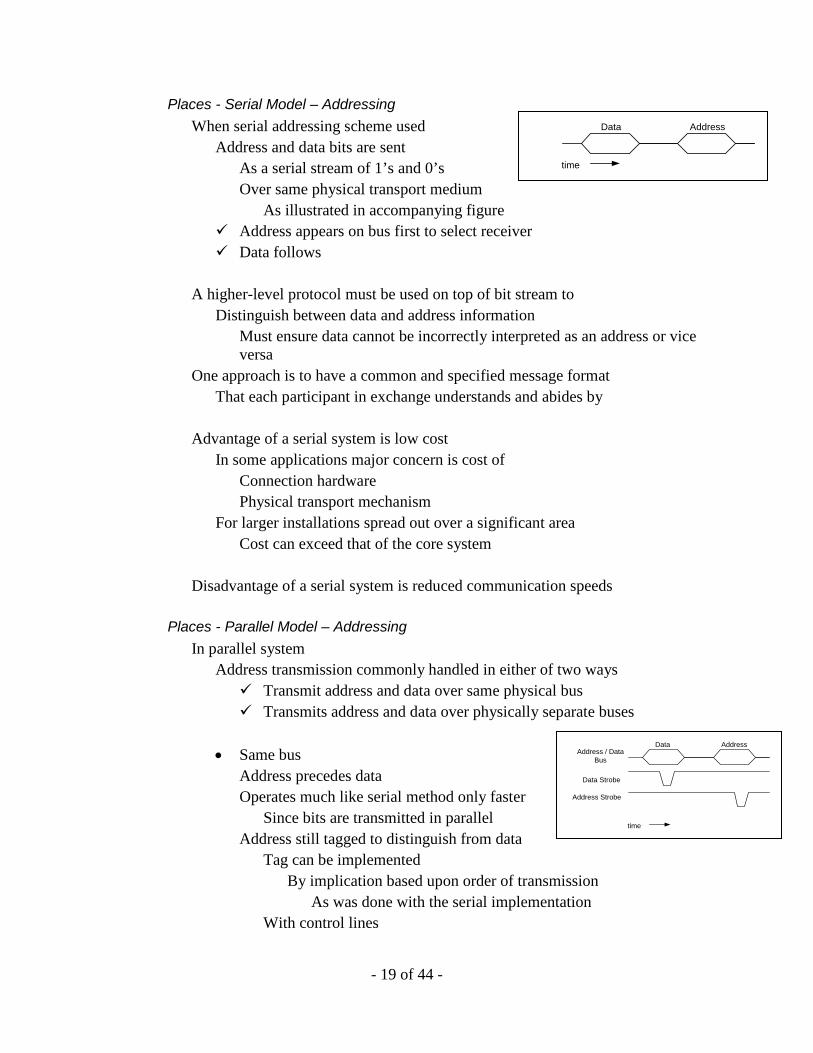
Places - Serial Model – Addressing When serial addressing scheme used
Address and data bits are sent As a serial stream of 1’s and 0’s Over same physical transport medium
As illustrated in accompanying figure Address appears on bus first to select receiver Data follows
A higher-level protocol must be used on top of bit stream to
Distinguish between data and address information Must ensure data cannot be incorrectly interpreted as an address or vice versa
One approach is to have a common and specified message format That each participant in exchange understands and abides by
Advantage of a serial system is low cost In some applications major concern is cost of
Connection hardware Physical transport mechanism
For larger installations spread out over a significant area Cost can exceed that of the core system
Disadvantage of a serial system is reduced communication speeds
Places - Parallel Model – Addressing
In parallel system Address transmission commonly handled in either of two ways Transmit address and data over same physical bus Transmits address and data over physically separate buses
• Same bus
Address precedes data Operates much like serial method only faster
Since bits are transmitted in parallel Address still tagged to distinguish from data
Tag can be implemented By implication based upon order of transmission
As was done with the serial implementation With control lines
Data Address
time
Address / DataBus
Data Address
Data Strobe
Address Strobe
time
- 20 of 44 -
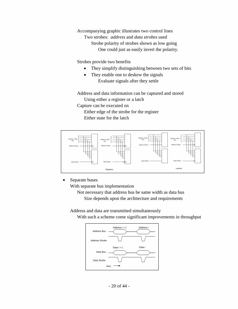
Accompanying graphic illustrates two control lines Two strobes: address and data strobes used
Strobe polarity of strobes shown as low going One could just as easily invert the polarity.
Strobes provide two benefits
• They simplify distinguishing between two sets of bits • They enable one to deskew the signals
Evaluate signals after they settle Address and data information can be captured and stored
Using either a register or a latch Capture can be executed on
Either edge of the strobe for the register Either state for the latch
• Separate buses With separate bus implementation
Not necessary that address bus be same width as data bus Size depends upon the architecture and requirements
Address and data are transmitted simultaneously
With such a scheme come significant improvements in throughput
Address / DataBus
Address Strobe
Data Strobe
Address / DataBus
Address Strobe
Data Strobe
Address / DataBus
Address Strobe
Data Strobe
Address / DataBus
Address Strobe
Data Strobe
Registers Latches
Address BusAddress i + 1
Data i + 1
Data Strobe
Address i
Data i
Data Bus
Address Strobe
time
- 21 of 44 -
Strobes are still essential Each identifies when signals on bus are stable and valid Without a strobe
No way to properly interpret values of the signals
Control Number and structure depend upon nature of system Typical signals may include
Read / Write Address / Data present or stable Clock
Where does the clock come from Separate line Encoded in the data
Transmission Direction Ready or Active Synchronize Reset Power
May or may not be counted as control signal Information - Data
Whether realized as a serial or parallel bus Data lines carry information to be transmitted or received
When implemented in parallel will typically carry one word per transfer For a system with 32 bit words
Data bus will be 32 bits wide Carry DB0 - DB31
Important to determine Which bit is MSB and which is LSB Whether the data is positive or negative true
Transport
The physical transport of information between system core and local external devices Can utilize any of schemas discussed Today most frequently copper wire used
Clearly changing to fiber and air
- 22 of 44 -
Implementing the Local Device Model – A First Step Design serves as basis for look at
Interacting with outside world signals As we’ve noted embedded systems
Designed to perform some task Performing task means interfacing with world outside processor Such tasks may include
Making measurements Controlling motor Running telecommunication system
We are dealing with portions of von Neumann machine
Designated Input and Output Memory
When consider memory mapped I/O Our exchange with outside world
• Synchronous Based upon some timing element
• Asynchronous Start of and subsequent transactions temporally independent
From our model
When studying processor input and output Know we must look at several things
• Data source or destination - Places I/O ports Memory address space
• Nature of the exchange - Control Three types possible
Event Shared variable Message
Note Such exchange also occurs between / among
Tasks within same processor • Where I/O procedure resides • How I/O procedure invoked - Control
Associated restrictions
- 23 of 44 -
• Protocol for the data exchange - Control • Timing requirements - Control
Let’s look at each of these
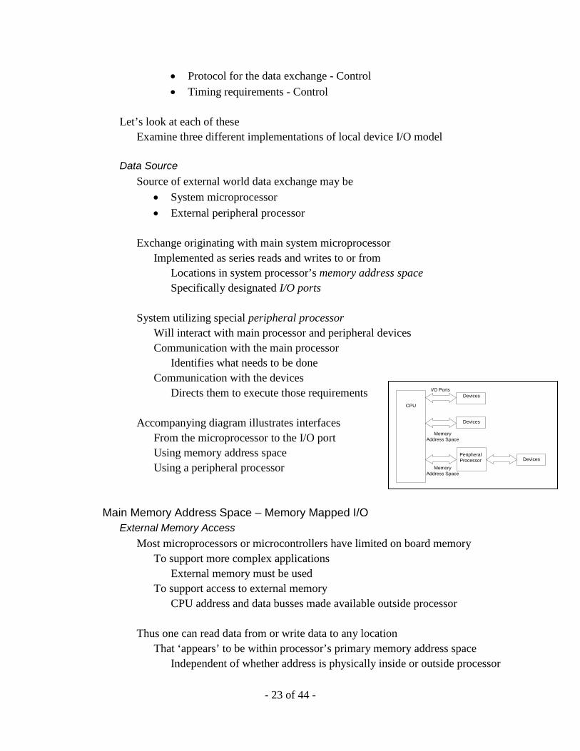
Examine three different implementations of local device I/O model Data Source
Source of external world data exchange may be • System microprocessor • External peripheral processor
Exchange originating with main system microprocessor
Implemented as series reads and writes to or from Locations in system processor’s memory address space Specifically designated I/O ports
System utilizing special peripheral processor
Will interact with main processor and peripheral devices Communication with the main processor
Identifies what needs to be done Communication with the devices
Directs them to execute those requirements Accompanying diagram illustrates interfaces
From the microprocessor to the I/O port Using memory address space Using a peripheral processor
Main Memory Address Space – Memory Mapped I/O
External Memory Access Most microprocessors or microcontrollers have limited on board memory
To support more complex applications External memory must be used
To support access to external memory CPU address and data busses made available outside processor
Thus one can read data from or write data to any location
That ‘appears’ to be within processor’s primary memory address space Independent of whether address is physically inside or outside processor
CPU
I/O Ports
Memory Address Space
Peripheral Processor Devices
Devices
Devices
Memory Address Space
- 24 of 44 -
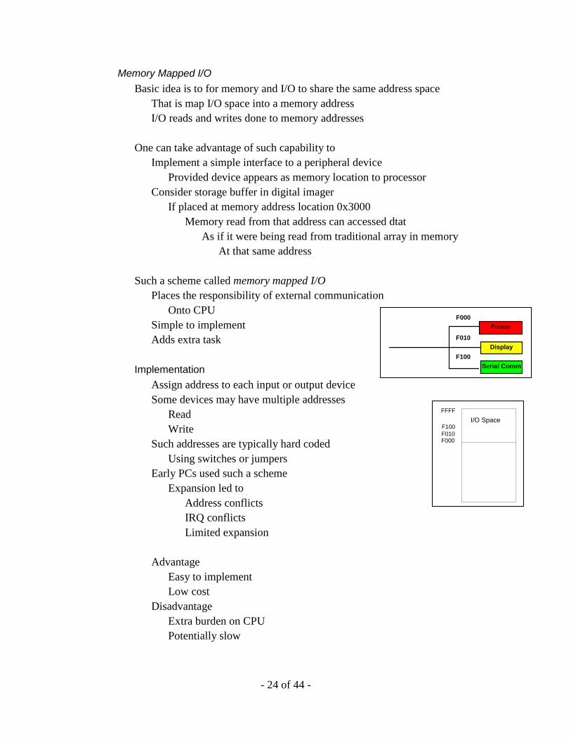
Memory Mapped I/O Basic idea is to for memory and I/O to share the same address space
That is map I/O space into a memory address I/O reads and writes done to memory addresses
One can take advantage of such capability to Implement a simple interface to a peripheral device
Provided device appears as memory location to processor Consider storage buffer in digital imager
If placed at memory address location 0x3000 Memory read from that address can accessed dtat
As if it were being read from traditional array in memory At that same address
Such a scheme called memory mapped I/O
Places the responsibility of external communication Onto CPU
Simple to implement Adds extra task
Implementation
Assign address to each input or output device Some devices may have multiple addresses
Read Write
Such addresses are typically hard coded Using switches or jumpers
Early PCs used such a scheme Expansion led to
Address conflicts IRQ conflicts Limited expansion
Advantage
Easy to implement Low cost
Disadvantage Extra burden on CPU Potentially slow
Printer
Serial Comm
F000
F010
F100Display
I/O Space
F000F010F100
FFFF
- 25 of 44 -
I/O Ports – Programmed Controlled I/O On many microcontrollers or microcomputers
Number of pins specifically dedicated to Bringing data into processor Sending data out of processor
Collectively referred to as I/O Ports Are different from the external memory bus For specific processor lines may be designated as
• Unidirectional - Input or Output Tend to be static Direction is established in hardware
Usually done during initialization • Bi-directional - Input and Output
Bi-directional lines are dynamic Direction is selected under program control
Based upon the nature of the transaction Usually such signals grouped in sets of 4 or 8 lines Direction set for entire group
Processor lines designated as bi-directional
May support tri-state capability If so may have ‘weak pull-up’ associated with each line
Defines state of line under tri-state condition
Information exchange based upon specifically designated I/O ports Called Program Controlled I/O • Advantage over memory mapped I/O
Does not use any of the main memory addresses Eliminates dual use of memory address and data busses
• Disadvantage is control of any exchanges with peripheral devices Remains under auspices of main CPU
- 26 of 44 -
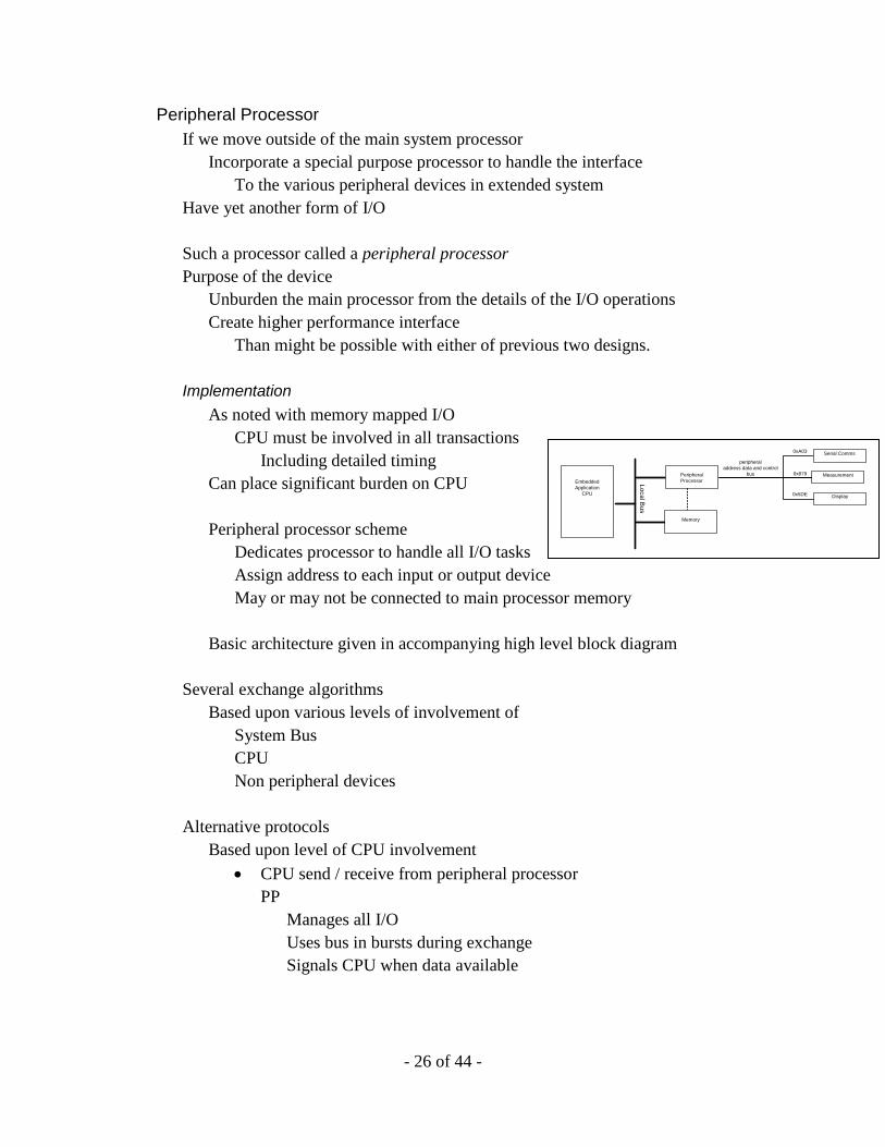
Peripheral Processor If we move outside of the main system processor
Incorporate a special purpose processor to handle the interface To the various peripheral devices in extended system
Have yet another form of I/O Such a processor called a peripheral processor Purpose of the device
Unburden the main processor from the details of the I/O operations Create higher performance interface
Than might be possible with either of previous two designs.
Implementation As noted with memory mapped I/O
CPU must be involved in all transactions Including detailed timing
Can place significant burden on CPU Peripheral processor scheme
Dedicates processor to handle all I/O tasks Assign address to each input or output device May or may not be connected to main processor memory
Basic architecture given in accompanying high level block diagram
Several exchange algorithms Based upon various levels of involvement of
System Bus CPU Non peripheral devices
Alternative protocols Based upon level of CPU involvement
• CPU send / receive from peripheral processor PP
Manages all I/O Uses bus in bursts during exchange Signals CPU when data available
0xA03 Serial Comms
Measurement
Display
0x879
0x5DE
peripheraladdress data and control
busEmbedded Application
CPU
Peripheral Processor
Memory
Local Bus
- 27 of 44 -
• CPU tells peripheral processor where to find / put data in memory PP
Exchanges data with memory Manages all I/O Signals CPU when data available Uses bus
In bursts during exchange For duration of exchange
DMA Using address passing and shared buffer
• CPU enables non-peripheral device and peripheral processor to
communicate PP
Exchanges data with device Manages all I/O Signals Device when data available May signal CPU when complete Uses bus
In bursts during exchange For duration of exchange
Acts as surrogate for main CPU Advantage
I/O speed independent of CPU Unburdens CPU
Disadvantage Higher cost Complex
Control and Synchronization
Similar to internal exchange Three types external interchange possible Event Shared Variable Message
Observe these are abstractions Within each type
Variety of related signals
- 28 of 44 -
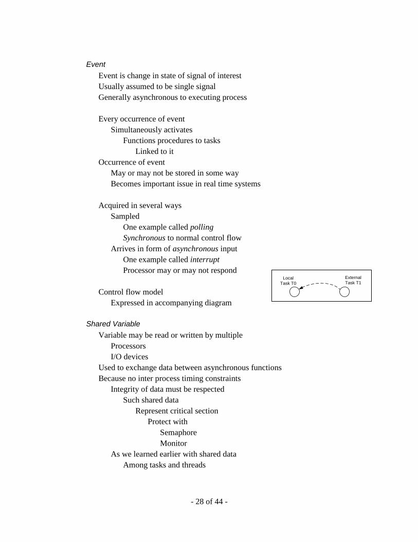
Event
Event is change in state of signal of interest Usually assumed to be single signal Generally asynchronous to executing process Every occurrence of event
Simultaneously activates Functions procedures to tasks
Linked to it Occurrence of event
May or may not be stored in some way Becomes important issue in real time systems
Acquired in several ways
Sampled One example called polling Synchronous to normal control flow
Arrives in form of asynchronous input One example called interrupt Processor may or may not respond
Control flow model
Expressed in accompanying diagram
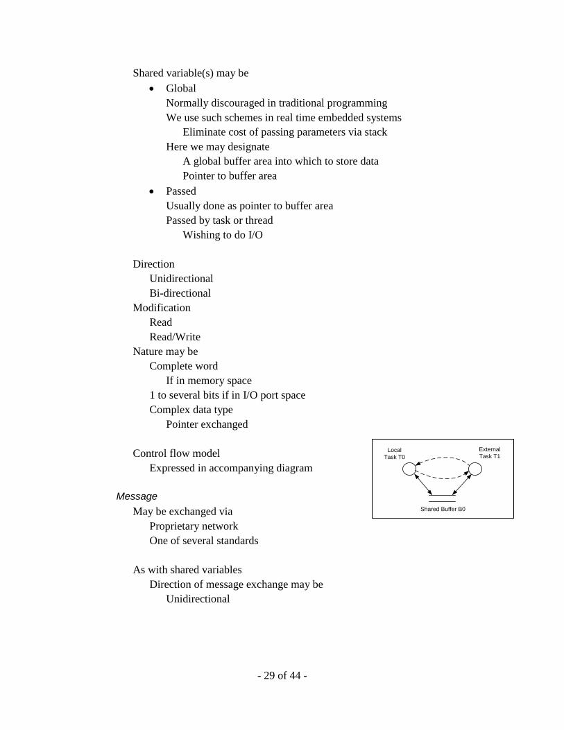
Shared Variable Variable may be read or written by multiple
Processors I/O devices
Used to exchange data between asynchronous functions Because no inter process timing constraints
Integrity of data must be respected Such shared data
Represent critical section Protect with
Semaphore Monitor
As we learned earlier with shared data Among tasks and threads
External Task T1
Local Task T0
- 29 of 44 -
Shared variable(s) may be • Global
Normally discouraged in traditional programming We use such schemes in real time embedded systems
Eliminate cost of passing parameters via stack Here we may designate
A global buffer area into which to store data Pointer to buffer area
• Passed Usually done as pointer to buffer area Passed by task or thread
Wishing to do I/O
Direction Unidirectional Bi-directional
Modification Read Read/Write
Nature may be Complete word
If in memory space 1 to several bits if in I/O port space Complex data type
Pointer exchanged Control flow model
Expressed in accompanying diagram Message
May be exchanged via Proprietary network One of several standards
As with shared variables
Direction of message exchange may be Unidirectional
Shared Buffer B0
External Task T1
Local Task T0
- 30 of 44 -
Bi-directional Intent may be
Read Read/Write
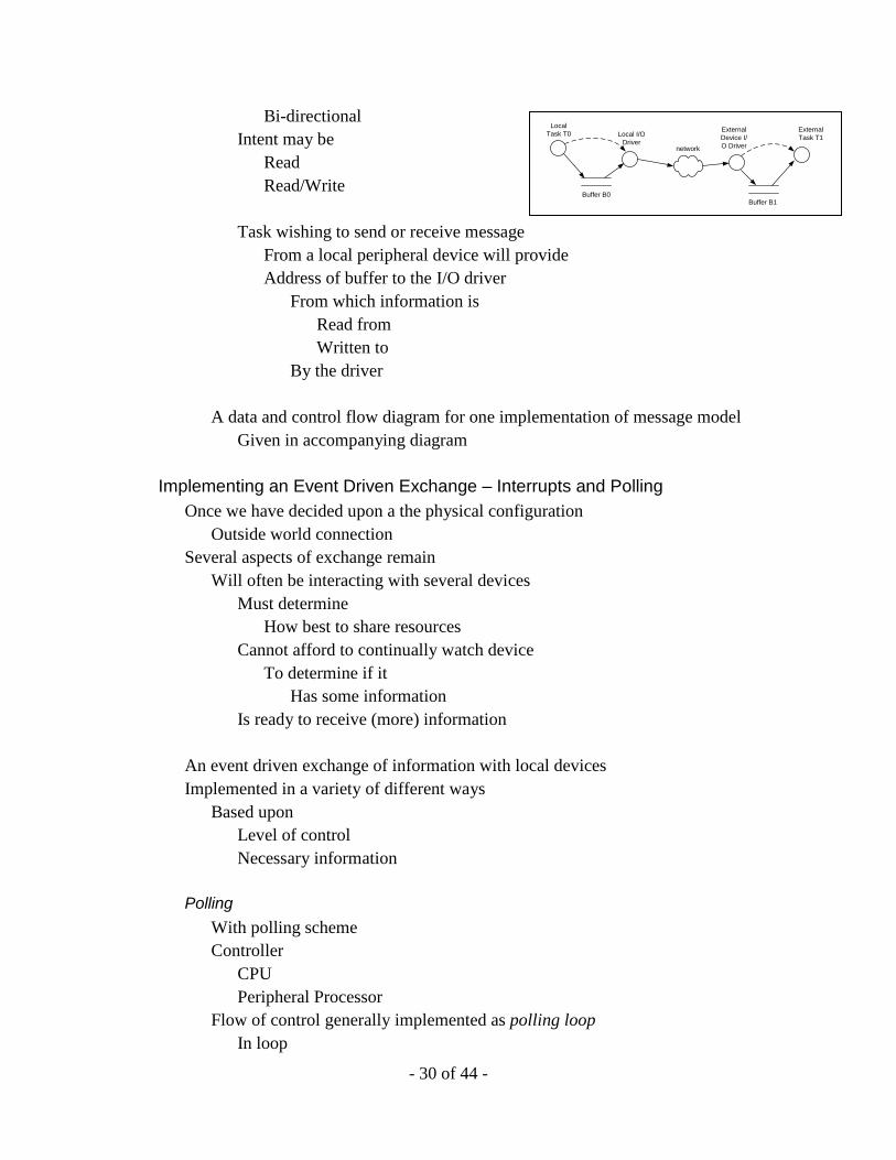
Task wishing to send or receive message
From a local peripheral device will provide Address of buffer to the I/O driver
From which information is Read from Written to
By the driver
A data and control flow diagram for one implementation of message model Given in accompanying diagram
Implementing an Event Driven Exchange – Interrupts and Polling
Once we have decided upon a the physical configuration Outside world connection
Several aspects of exchange remain Will often be interacting with several devices
Must determine How best to share resources
Cannot afford to continually watch device To determine if it
Has some information Is ready to receive (more) information
An event driven exchange of information with local devices Implemented in a variety of different ways
Based upon Level of control Necessary information
Polling
With polling scheme Controller
CPU Peripheral Processor
Flow of control generally implemented as polling loop In loop
network
External Task T1
Local Task T0
Buffer B0
Local I/O Driver
Buffer B1
External Device I/O Driver
- 31 of 44 -
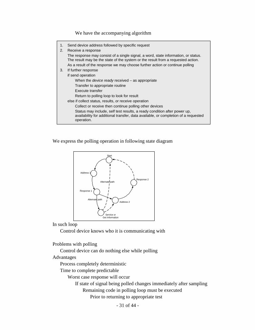
We have the accompanying algorithm
We express the polling operation in following state diagram
In such loop Control device knows who it is communicating with
Problems with polling
Control device can do nothing else while polling Advantages
Process completely deterministic Time to complete predictable
Worst case response will occur If state of signal being polled changes immediately after sampling
Remaining code in polling loop must be executed Prior to returning to appropriate test
1. Send device address followed by specific request 2. Receive a response
The response may consist of a single signal, a word, state information, or status. The result may be the state of the system or the result from a requested action. As a result of the response we may choose further action or continue polling
3. If further response if send operation
When the device ready received – as appropriate Transfer to appropriate routine Execute transfer Return to polling loop to look for result
else if collect status, results, or receive operation Collect or receive then continue polling other devices Status may include, self test results, a ready condition after power up,
availability for additional transfer, data available, or completion of a requested operation.
Start
Address 1
Address 2
Response 2
Response 1
Service orGet Information
Alternate path
Alternate path
- 32 of 44 -
In real-time systems with hard deadline Being able to analyze and to quantify the flow of control
Absolutely essential Interrupt
Goal of interrupt scheme same as that of polled scheme Difference
Control device not dedicated to monitoring external devices I/O system may have from 1 to many interrupt lines Each line may be connected to 1 or several devices
Single Interrupt Line with Single Device Let’s first examine how single interrupt might work As name suggests
Interrupt signal interrupts foreground activity When interrupt occurs several actions possible
Ignore Respond
Ignore Will discuss shortly
Respond Responding to interrupt much like subroutine call Procedure
1. Suspend current process 2. Save the current context 3. Acknowledge the interrupt 4. Branch to the ISR appropriate to interrupting device 5. Execute the routine 6. Restore the former context and resume former process
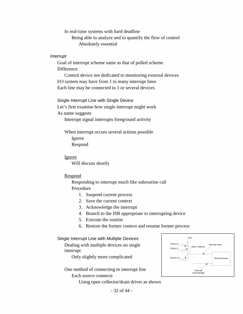
Single Interrupt Line with Multiple Devices
Dealing with multiple devices on single interrupt
Only slightly more complicated One method of connecting to interrupt line
Each source connects Using open collector/drain driver as shown
Vcc
Device 0
Device 1
Device n-1
Open Collector
Microprocessor
Interrupt Input
InterruptAcknowledge
- 33 of 44 -
In responding to the event
CPU issues acknowledge informing interrupting device • Interrupt has been recognized • Handling process will begin
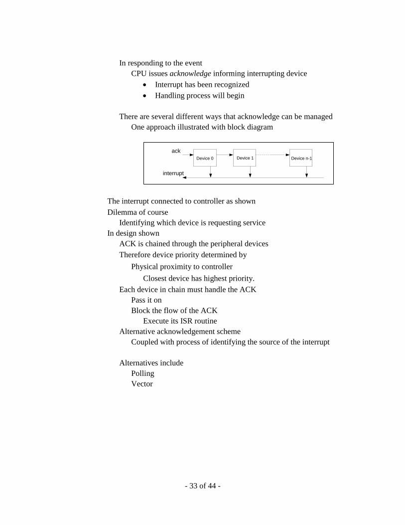
There are several different ways that acknowledge can be managed
One approach illustrated with block diagram
The interrupt connected to controller as shown Dilemma of course
Identifying which device is requesting service In design shown
ACK is chained through the peripheral devices Therefore device priority determined by
Physical proximity to controller Closest device has highest priority.
Each device in chain must handle the ACK Pass it on Block the flow of the ACK
Execute its ISR routine Alternative acknowledgement scheme
Coupled with process of identifying the source of the interrupt Alternatives include
Polling Vector
ack
interrupt
Device 0 Device 1 Device n-1
- 34 of 44 -
Polling Straight forward Sequence
1. Interrupt occurs 2. Suspend current task 3. Branch to handler
Poll devices to identify Branch to appropriate handler routine
Handle Return
4. Resume suspended task
Vector With vector scheme Device requesting service
1. Interrupts 2. When acknowledged
Returns identifier Device name Address of service routine
3. Sequence then proceeds as with polled alternative
Multiple With several devices on the same line Must now address question
How to accommodate multiple Simultaneous interrupts Sequential interrupts
• Simultaneous Must have priority scheme Can be
Physical proximity Assigned
Higher priority device gets serviced first
- 35 of 44 -
• Sequential If second interrupt occurs while handling first
Ignore until finished with first Assign each device priority
If interrupting device has higher priority Handle in same way Similar to calling subroutine from subroutine
Multiple Interrupt Lines with Single Device on Each
For each line Same as single line with single device
With multiple lines Must assign priority to each Same as single line with multiple devices
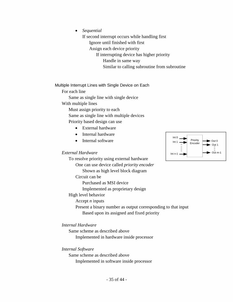
Priority based design can use • External hardware • Internal hardware • Internal software
External Hardware
To resolve priority using external hardware One can use device called priority encoder
Shown as high level block diagram Circuit can be
Purchased as MSI device Implemented as proprietary design
High level behavior Accept n inputs Present a binary number as output corresponding to that input
Based upon its assigned and fixed priority Internal Hardware
Same scheme as described above Implemented in hardware inside processor
Internal Software
Same scheme as described above Implemented in software inside processor
Int 0
Int 1
Int n-1
Out 0Out 1
Out m-1
PriorityEncoder
- 36 of 44 -
Multiple Interrupt Lines with Multiple Devices on Each For each line
Same as single line with multiple devices With multiple lines
Must assign priority to each Same as single line with multiple devices
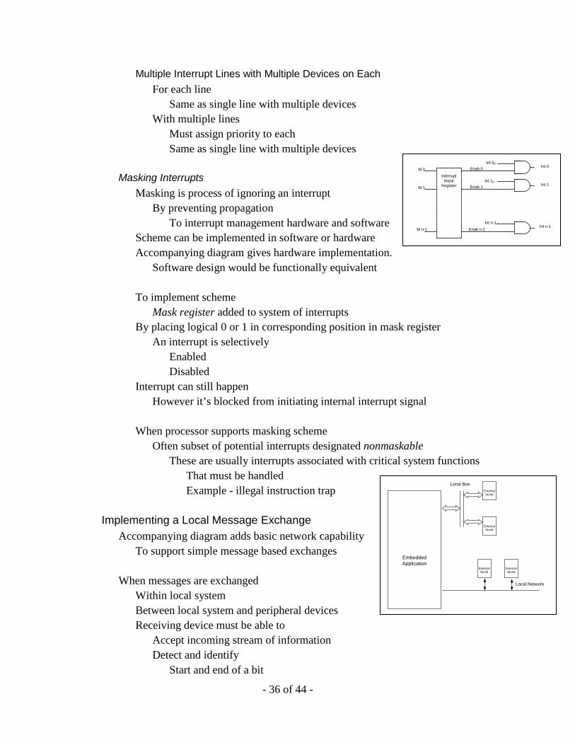
Masking Interrupts
Masking is process of ignoring an interrupt By preventing propagation
To interrupt management hardware and software Scheme can be implemented in software or hardware Accompanying diagram gives hardware implementation.
Software design would be functionally equivalent To implement scheme
Mask register added to system of interrupts By placing logical 0 or 1 in corresponding position in mask register
An interrupt is selectively Enabled Disabled
Interrupt can still happen However it’s blocked from initiating internal interrupt signal
When processor supports masking scheme
Often subset of potential interrupts designated nonmaskable These are usually interrupts associated with critical system functions
That must be handled Example - illegal instruction trap
Implementing a Local Message Exchange Accompanying diagram adds basic network capability
To support simple message based exchanges
When messages are exchanged Within local system Between local system and peripheral devices Receiving device must be able to
Accept incoming stream of information Detect and identify
Start and end of a bit
Int 0in
Int 1in
Int n-1in
Enab 0
Enab 1
Enab n-1
M 0
M 1
M n-1
InterruptMask
Register
Int 0
Int 1
Int n-1
Embedded Application
External World
External World
External World
External World
Local Bus
Local Network
- 37 of 44 -
Start and end of a character Start and end of a message block or frame
These are known as • Bit • Character • Frame synchronization
Different transmission modes
Give rise to two general categories of message exchange Asynchronous transmission
Receiver resynchronizes at start of each bit Synchronous transmission
Receiver resynchronizes Continuously based upon encoded clock edge transitions Start of each block or frame
Asynchronous Transmission Characterized by irregular intervals between transmitted data groups Inter character spacing may vary widely May be bursts of activity
Followed by long periods of inactivity Synchronous Transmission
When blocks of regularly spaced data Transferred over a serial line
Transmitter and receiver can be synchronized to common clock Permitting character transfer at much higher rate
Generally synchronous transfer requires less overhead
Therefore is more efficient than asynchronous design Asynchronous Exchange
Because no inherent clock associated with asynchronous exchange Coordination and synchronization accomplished
Using protocol that permits (re)synchronization of data To receiving system’s internal clock
Both the protocols and amount of data exchanged can vary tremendously
- 38 of 44 -
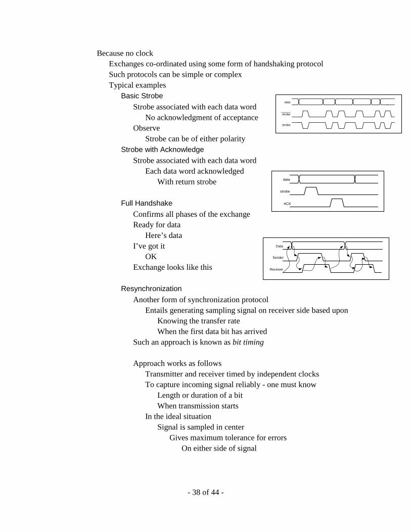
Because no clock Exchanges co-ordinated using some form of handshaking protocol Such protocols can be simple or complex Typical examples
Basic Strobe Strobe associated with each data word
No acknowledgment of acceptance Observe
Strobe can be of either polarity Strobe with Acknowledge
Strobe associated with each data word Each data word acknowledged
With return strobe Full Handshake
Confirms all phases of the exchange Ready for data
Here’s data I’ve got it
OK Exchange looks like this
Resynchronization
Another form of synchronization protocol Entails generating sampling signal on receiver side based upon
Knowing the transfer rate When the first data bit has arrived
Such an approach is known as bit timing Approach works as follows
Transmitter and receiver timed by independent clocks To capture incoming signal reliably - one must know
Length or duration of a bit When transmission starts
In the ideal situation Signal is sampled in center
Gives maximum tolerance for errors On either side of signal
data
strobe
strobe
Data
Sender
Receiver
data
strobe
ACK
- 39 of 44 -
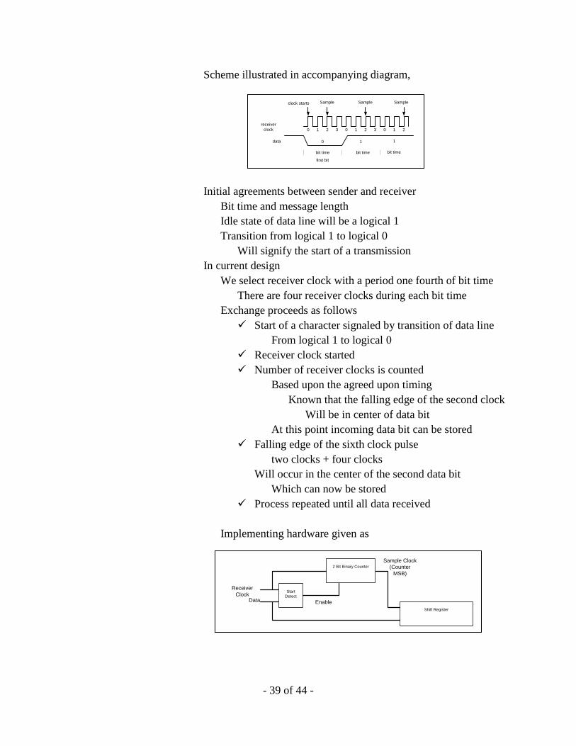
Scheme illustrated in accompanying diagram,
Initial agreements between sender and receiver
Bit time and message length Idle state of data line will be a logical 1 Transition from logical 1 to logical 0
Will signify the start of a transmission In current design
We select receiver clock with a period one fourth of bit time There are four receiver clocks during each bit time
Exchange proceeds as follows Start of a character signaled by transition of data line
From logical 1 to logical 0 Receiver clock started Number of receiver clocks is counted
Based upon the agreed upon timing Known that the falling edge of the second clock
Will be in center of data bit At this point incoming data bit can be stored
Falling edge of the sixth clock pulse two clocks + four clocks
Will occur in the center of the second data bit Which can now be stored
Process repeated until all data received Implementing hardware given as
Sample
data
receiver clock
clock starts Sample Sample
0 1 2 3 0 1 2 3 0 1 2
bit time bit time bit time
0 1 1
first bit
Receiver Clock
Data
Sample Clock(Counter
MSB)
StartDetect
Shift Register
2 Bit Binary Counter
Enable
- 40 of 44 -
Analysis of Asynchronous Exchange Potential problems
• Difficult to test • Clock noise more difficult to filter out • Potentially complex protocol
To identify start / end of transmission
Potential advantages • Devices may run at different / differing speed • No clock skew on long busses
Synchronous Exchange There are several drawbacks of the asynchronous transmission schemes
• Extra overhead of control bits • Bit clock synchronization scheme less reliable at higher data rates
Problems can be mitigated with synchronous transmission Still must achieve
Bit, character, frame synchronization Frame synchronization usually derived from the former Generally includes clock in control lines
Exchanges between sender and receiver
Synchronized to the clock • Directly • Signals derived from the clock
Manchester phase encoding Serial Exchange
Clock either separate or encoded in data Parallel Exchange
Clock one of control lines
Bit Synchronization To achieve bit synchronization
Two step typically used • Encode the clock in the data • Re-derive the clock from the data
- 41 of 44 -
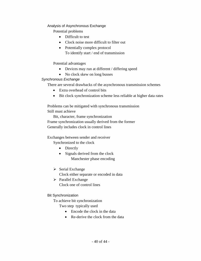
Encoded Clock Three different methods generally used
Bipolar Encoding
Binary 0’s and 1’s are represented by Different polarity signals
Each bit cell contains clocking information Observe
Signal returns to zero level after each encoded bit Referred to as return-to-zero RZ signal
Scheme requires 3 distinct signal levels
Manchester Phase Encoding
Binary 0 - high to low signal transition Binary 1 - low to high signal transition Transition in the center of each bit cell
0 → 1 // indicates a 1 1 → 0 // indicates a 0 Provides the clock information
Observe Signal does not return to zero level after each encoded bit Referred to as non-return-to-zero NRZ signal
Manchester Differential Encoding
Transition in the center of each bit cell 0 → 1 1 → 0 Provides the clock information
Transition At the start of each bit cell
Only if next bit to be encoded is a binary 0 Otherwise in center
Re-derive the Clock To re-derive clock from data
Transmission begins with a preamble Including a synchronization sequence
A phase locked loop - PLL Based upon a very stable receiver clock Used to keep sample clock locked to incoming signal transitions
- 42 of 44 -
Data must be encoded To ensure a sufficient number of signal transitions
To retain synchronization At each transition
Sample timing adjusted to ensure sampling in center of bit Design will tolerate intervals without transitions
Provided there is a stable fundamental clock
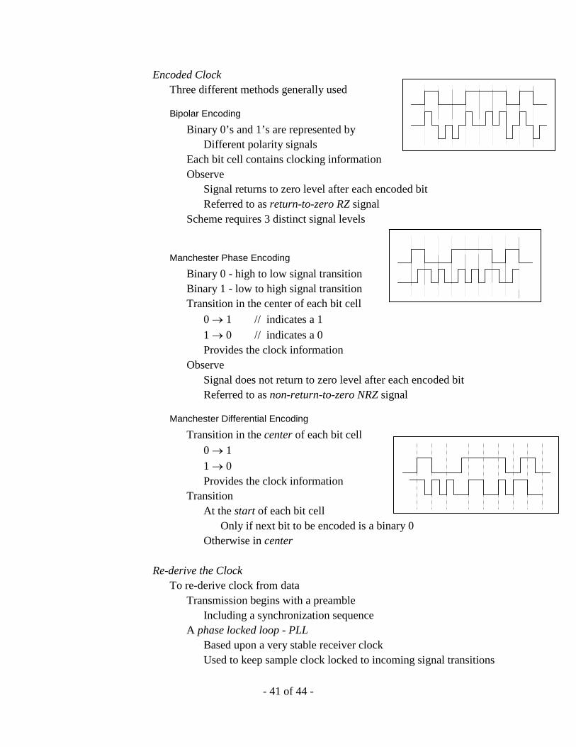
PLL is a conventional closed loop control system With some additions and modifications
Basic structure for a closed loop system given following diagram
For traditional analog closed loop control system
Input is algebraically added to a signal that is Modified and fed back from system output
Result is an error signal That serves as an input to the system under control
Objective is to drive the error signal to zero For phase locked loop
Objective is to control a frequency Basic block diagram appears as
Output of the PLL generated
Using a voltage controlled oscillator (VCO) Output of VCO is fed back to a phase detector
That compares Input signal characteristics with
System Under Control
Feedback
Input Output
Filter VCOPhase Detection
Amp
Output Frequency
- 43 of 44 -
Those of signal being fed back When the frequency and phase difference
Between input signal and VCO output is zero System has locked onto input frequency
Difference in frequency and phase appears as an error voltage Error signal is filtered by the low pass filter Amplified Provides an input voltage to the VCO
Output of VCO can now serve as clock to the system Input signal to the PLL is
Any of the encoded data streams Use a preamble including sync sequence Done using phase lock loop- PLL Based upon very stable receiver clock PLL used to keep sample clock locked
Signal transitions of incoming signal Data encoded to ensure a sufficient number of signal transitions At each transition sample timing adjusted to ensure
Sampling in center of bit Scheme will tolerate intervals without transitions
Based upon stability of the clock Bit / Character / Frame Synchronization
Once individual bits are identified Character and frame synchronization rather straight forward
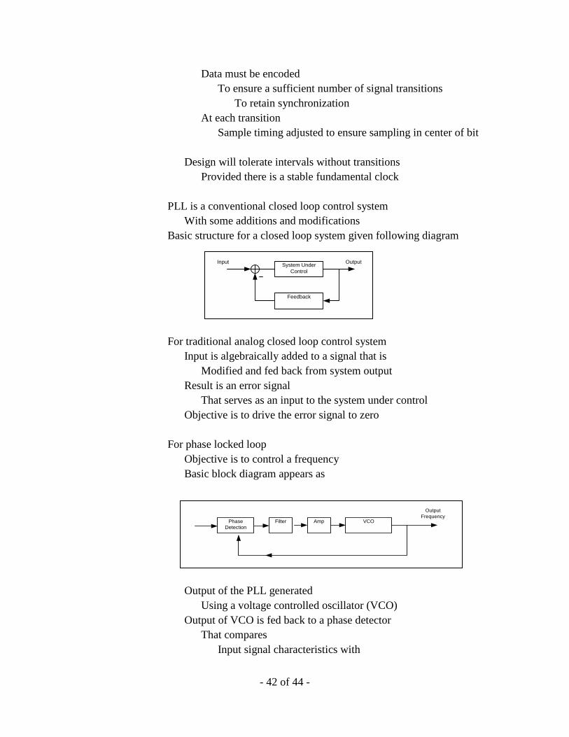
Analysis of Synchronous Exchange Potential problems
• All devices must run at same speed • Can have different propagation delays along a bus
Because of (potentially) different loading on clock vs. data lines • Clock skew on long busses
Because of different loading Have propagation delay along bus
Possibility that clock will arrive at the various destinations
At different times with respect to the data As illustrated
One can easily get clock skew (with respect to the data)
Data
Clock
Clock
Data
t0
t0
module 0
module n-1

- 44 of 44 -
On long busses Particularly at higher clocking frequencies
Potential advantages
• Easier to test • Generally protocol is simpler that asynchronous approach • Easier to stay in sync with data