Embed Size (px)
Citation preview

Ultra-Wideband Antenna in Coplanar Technology
by
Hung-Jui Lam B.Eng., University of Victoria, 2005
A Thesis Submitted in Partial Fulfillment of the
Requirements for the Degree of
MASTER OF APPLIED SCIENCE
In the Department of Electrical and Computer Engineering
© Hung-Jui Lam, 2007 University of Victoria
All rights reserved. This thesis may not be reproduced in whole or in part, by
photocopy or other means, without the permission of the author.
ii
Ultra-Wideband Antenna in Coplanar Technology
by
Hung-Jui Lam B.Eng., University of Victoria, 2005
Supervisory Committee Dr. Jens Bornemann Supervisor, Department of Electrical and Computer Engineering Dr. Thomas E. Darcie Departmental Member, Department of Electrical and Computer Engineering Dr. Edward J. Park Outside Member, Department of Mechanical Engineering Dr. Zuomin Dong External Examiner, Department of Mechanical Engineering

iii
ABSTRACT
Ultra-wideband (UWB) antennas are one of the most important elements for UWB
systems. With the release of the 3.1 - 10.6 GHz band, applications for short-range and
high-bandwidth handheld devices are primary research areas in UWB systems. Therefore,
the realization of UWB antennas in printed-circuit technologies within relatively small
substrate areas is of primary importance.
This thesis focuses on the design of a new UWB antenna based on coplanar
technology. Compared with microstrip circuitry, coplanar technology achieves easier
fabrication and wider antenna bandwidth. Two professional full-wave field solver
software packages, HFSS and MEFiSTo-3D, are used as analysis tools to obtain antenna
performances.
A new printed-circuit antenna in coplanar technology for UWB systems is
introduced. The frequency of operation is 3.1 GHz to 10.6 GHz with a VSWR < 2. Nearly
omni-directional characteristics in vertical polarization are demonstrated at selected
frequencies. Relatively good group delay characteristics are obtained and compare well
with other published UWB antenna designs.

iv
Table of Contents
Supervisory Committee .................................................................................................... ii
ABSTRACT...................................................................................................................... iii
Table of Contents...............................................................................................................iv
List of Tables......................................................................................................................vi
List of Figures.................................................................................................................. vii
Acknowledgments ........................................................................................................... xii
Dedication ....................................................................................................................... xiii
1.0 Introduction..................................................................................................................1
1.1 Purpose of Thesis .......................................................................................................2 1.2 Organization of Thesis ...............................................................................................3 1.3 Contributions..............................................................................................................5
2.0 Fundamentals of Ultra-Wideband Technology .........................................................6
2.1 General Overview ......................................................................................................6 2.2 Development of Ultra-Wideband Technology and Antennas ....................................9
2.2.1 History.................................................................................................................9 2.2.2 History of Ultra-Wideband Antennas................................................................12
2.3 Ultra-Wideband Antennas........................................................................................20 2.3.1 Introduction to Ultra-Wideband Antennas ........................................................20 2.3.2 Directionality and Different Types of Antennas ...............................................22 2.3.3 Matching and Spectral Control .........................................................................24 2.3.4 Directivity and System Performance ................................................................27 2.3.5 Antenna Dispersion...........................................................................................32
3.0 UWB Printed-Circuit-Board (PCB) Antennas ........................................................38
3.1 Introduction to UWB PCB Antennas .......................................................................38 3.2 Microstrip UWB Antennas ......................................................................................43 3.3 Coplanar Waveguide (CPW) UWB Antennas..........................................................49 3.4 Comparison between Mirostrip and CPW UWB Antennas .....................................57

v
4.0 UWB Coplanar Waveguide Antennas ......................................................................58
4.1 The First Design.......................................................................................................58 4.2 Different Design Approaches...................................................................................61 4.3 The Final Design......................................................................................................66 4.4 Final Design Results ................................................................................................68
4.4.1 HFSS Simulation Model ...................................................................................68 4.4.2 HFSS Simulation Results..................................................................................75 4.4.3 MEFiSTo-3D Simulation Model.......................................................................81 4.4.4 MEFiSTo-3D Simulation Results .....................................................................88
4.5 The Improved Final Design .....................................................................................97
5.0 Conclusions and Further Work ..............................................................................104
5.1 Conclusions............................................................................................................104 5.2 Further Work ..........................................................................................................106
References .......................................................................................................................108

vi
List of Tables
Table 2.3.1 : Trade-offs between directional and omni antennas (from [49])....................23 Table 3.4.1: Summary of comparison between microstrip and CPW-fed UWB antenna
examples. ...................................................................................................................57 Table 4.3.1: Dimensional values of the proposed UWB antenna. .....................................66

vii
List of Figures
Fig. 2.2.1: Lodge’s preferred antennas consisting of triangular “capacity areas,” a clear
precursor to the “bow tie” antenna (1898) (from [47])..............................................13 Fig. 2.2.2: Lodge’s bi-conical antennas (1898) (from [47])...............................................13 Fig. 2.2.3: Carter’s bi-conical antenna (1939) (from [47]). ...............................................14 Fig. 2.2.4: Carter’s conical monopole (1939) (from [47]). ................................................14 Fig. 2.2.5: Carter’s improved match bi-conical antenna (1939) (from [47]). ....................14 Fig. 2.2.6: Schelkunoff’s spherical dipole (1940) (from [47])...........................................14 Fig. 2.2.7: Lindenblad’s element in cross-section (1941) (from [47]). ..............................15 Fig. 2.2.8: A turnstile array of Lindenbald elements for television transmission (1941)
(from [47]). ................................................................................................................15 Fig. 2.2.9: Brillouin’s omni-directional coaxial horn (1948) (from [47])..........................16 Fig. 2.2.10: Brillouin’s directional coaxial horn (1948) (from [47]). ................................16 Fig. 2.2.11: Master’s diamond dipole (1947) (from [47])..................................................18 Fig. 2.2.12: (left) Stohr’s ellipsoidal monopole (1968) and (right) Stohr’s ellipsoidal
dipole (1968) (from [47])...........................................................................................18 Fig. 2.2.13: Lalezari’s broadband notch antenna (1989) (from [47]). ...............................18 Fig. 2.2.14: Thomas’s circular element dipole (1994) (from [47]). ...................................18 Fig. 2.2.15: Marié’s wide band slot antenna (1962) (from [47]). ......................................18 Fig. 2.2.16: Harmuth’s large current radiator (1985) (from [47])......................................19 Fig. 2.2.17: Barnes’s UWB slot antenna (2000) (from [47]). ............................................19 Fig. 2.3.1: A log periodic antenna (right) has a dispersive waveform, while an elliptical
dipole (left) has a non-dispersive waveform (from [49])...........................................22 Fig. 2.3.2: An isotropic antenna (left) has a gain of 0 dBi by definition. A small dipole
antenna (center) typically has a gain of about 2.2 dBi, and a horn antenna (right) may have a gain of 10 dBi or more (from [49]).................................................................23
Fig. 2.3.3: The continuously tapered slot horn elements of Nester (gray colorization on elements added) (from [49]). .....................................................................................25
Fig. 2.3.4: A hypothetical tapered horn antenna (top) with a transition from 50 Ω to 377 Ω (bottom) (from [49]). .................................................................................................25
Fig. 2.3.5: The relationship between antenna directivity and link performance for an omni TX to omni RX (top), an omni TX to directional RX (middle) and a directional TX

viii
to directional RX (bottom) (from [49])......................................................................32 Fig. 2.3.6: Log conical spiral antennas (from [50]). ..........................................................35 Fig. 2.3.7: Transmitted (left) and received (right) voltage waveform from a pair of conical
log spiral antennas (from [50]). .................................................................................35 Fig. 2.3.8: 1.25:1 axial ratio planar elliptical dipoles with 4.8x3.8 cm elements [50].......36 Fig. 2.3.9: Transmitted (left) and received (right) voltage waveform from a pair of planar
elliptical dipole antennas (from [50]). .......................................................................37 Fig. 3.1.1: Orientation of field components, both polarizations. .......................................41 Fig. 3.1.2: Simple phase center variation measurement layout (antenna at the bottom). ..43 Fig. 3.2.1: Top view (a) and back view (b) of the proposed UWB antenna from [10]. .....44 Fig. 3.2.2: Return loss in both simulation and measurement from [10]. ...........................45 Fig. 3.2.3: Measured antenna gain from [10].....................................................................45 Fig. 3.2.4: Measured radiation patterns at 3 GHz, xy-plane (left) and xz-plane (right) from
[10]. ............................................................................................................................46 Fig. 3.2.5: Measured group delay from [10]. .....................................................................46 Fig. 3.2.6: Layout of the proposed antenna from [12]. ......................................................47 Fig. 3.2.7: Return loss of both simulation and measurement from [12]. ...........................47 Fig. 3.2.8: Measured gain from [12]. .................................................................................47 Fig. 3.2.9: Measured radiation patterns in xz-plane and xy-plane from [12]. ...................48 Fig. 3.2.10: Measured group delay from [12]. ...................................................................49 Fig. 3.3.1: Layout of the proposed UWB antenna, (a) top view and (b) cross-section view
from [23]. ...................................................................................................................50 Fig. 3.3.2: Simulated and measured return loss from [23].................................................51 Fig. 3.3.3: Measured gain responses of the proposed UWB antenna at θ = -45o, 0o, 45o
and 90o in (a) E-plane and (b) H-plane from [23]......................................................52 Fig. 3.3.4: Measured and simulated radiation patterns of the CPW-fed antenna. (a) E (yz)
- plane and (b) H (xz) - plane from [23]. ...................................................................53 Fig. 3.3.5: Measured group delay at θ = -45o,0o, 45o and 90o in E-plane from [23]. .........54 Fig. 3.3.6: Layout of the proposed UWB antenna, top view and cross-section view from
[29]. ............................................................................................................................54 Fig. 3.3.7: Simulated and measured return loss from [29].................................................55 Fig. 3.3.8: Measured antenna peak gain from [29]. ...........................................................55 Fig. 3.3.9: Measured radiation patterns of the proposed UWB antenna from [29]. ..........56

ix
Fig. 4.1.1: Layout of the antenna from [14].......................................................................58 Fig. 4.1.2: Dimensions of the antenna from [14]. ..............................................................58 Fig. 4.1.3: VSWR of the antenna from [14].......................................................................59 Fig. 4.1.4: H-plane (xy-plane) radiation patterns, 4 - 7 GHz from [14]. ...........................59 Fig. 4.1.5: The layout of the CPW-fed antenna. ................................................................60 Fig. 4.1.6: VSWR performance of the CPW-fed antenna. .................................................60 Fig. 4.2.1: Layout of the first design approach. .................................................................62 Fig. 4.2.2: VSWR performance of the first design approach.............................................62 Fig. 4.2.3: Layout of the second design approach. ............................................................63 Fig. 4.2.4: VSWR performance of the second design approach. .......................................63 Fig. 4.2.5: Layout of the third design approach. ................................................................64 Fig. 4.2.6: VSWR performance of the third design approach............................................64 Fig. 4.2.7: Layout of the fourth design approach...............................................................65 Fig. 4.2.8: VSWR performance of the fourth design approach. ........................................65 Fig. 4.2.9: Comparisons of VSWR performances from the first to the fourth design
approaches..................................................................................................................65 Fig. 4.3.1: Detailed layout of the proposed UWB antenna in CPW technology................67 Fig. 4.4.1: VSWR performance (simulated and measured) of the UWB antenna presented
in [14].........................................................................................................................69 Fig. 4.4.2: VSWR performance (simulated and measured) of the UWB antenna presented
in [37].........................................................................................................................70 Fig. 4.4.3: E- and H-plane radiation patterns at 10 GHz (simulated and measured) of the
UWB antenna presented in [37].................................................................................70 Fig. 4.4.4: Final design model of proposed UWB antenna in HFSS. ................................71 Fig. 4.4.5: VSWR performance of the proposed final design UWB antenna in coplanar
waveguide technology................................................................................................76 Fig. 4.4.6: Maximum gain of the proposed final design UWB antenna in coplanar
waveguide technology................................................................................................76 Fig. 4.4.7: Normalized co-polarized H-plane (x-y plane) radiation patterns Eθ(π/2, φ) of
the coplanar UWB antenna for various frequencies. .................................................78 Fig. 4.4.8: Normalized cross-polarized H-plane (x-y plane) radiation patterns EΦ(π/2, φ)
of the coplanar UWB antenna for various frequencies. .............................................78

x
Fig. 4.4.9: Normalized co-polarized E-plane (y-z plane) radiation patterns Eθ(θ,π/2)) of the coplanar UWB antenna for various frequencies. .................................................79
Fig. 4.4.10: Normalized co-polarized E-plane (x-z plane) radiation patterns Eθ(θ,0) of the coplanar UWB antenna for various frequencies. .......................................................79
Fig. 4.4.11: Comparisons of VSWR performance for different relative dielectric constants.....................................................................................................................................80
Fig. 4.4.12: Comparison of VSWR performance between HFSS and MEFiSTo-3D for the proposed coplanar UWB antenna. .............................................................................83
Fig. 4.4.13: Comparison of VSWR performance between measurements, HFSS and MEFiSTo-3D for the UWB antenna in [15]...............................................................83
Fig. 4.4.14: Final design model of proposed UWB antenna in MEFiSTo-3D...................84 Fig. 4.4.15: Time-domain signal (a), amplitude spectrum (b) and phase spectrum (c) at the
input of the coaxial cable feeding the coplanar antenna (c.f. Fig. 4.4.14). ................89 Fig. 4.4.16: Radiated time-domain signal (a), amplitude spectrum (b) and phase spectrum
(c) detected by the probes; Eθ (solid lines) and Eφ (dashed lines). ............................90 Fig. 4.4.17: Radiated Eθ time-domain signal (a), amplitude spectrum (b) and phase
spectrum (c) detected by two sets of probes at the far field boundary (solid lines) and slightly within the far field boundary (dashed lines). ................................................91
Fig. 4.4.18: Amplitude response (a) and group-delay characteristic (b) of coplanar UWB antenna; vertical polarization Eθ (solid lines,) and horizontal polarization Eφ (dashed lines)...........................................................................................................................94
Fig. 4.4.19: Amplitude response (a) and group-delay characteristic (b) of the microstrip UWB antenna in [15]; vertical polarization Eθ (solid lines,) and horizontal polarization Eφ (dashed lines). ...................................................................................96
Fig. 4.5.1: Comparison of VSWR performances obtained with HFSS and MEFiSTo-3D
for the improved coplanar UWB antenna. .................................................................98 Fig. 4.5.2: Comparison of VSWR performances for different relative dielectric constants
of the improved UWB antenna design.......................................................................99 Fig. 4.5.3: Maximum gain of the improved UWB antenna in coplanar waveguide
technology. .................................................................................................................99 Fig. 4.5.4: Normalized co-polarized H-plane (x-y plane) radiation patterns Eθ(π/2, φ) of
the improved coplanar UWB antenna for various frequencies. ...............................100 Fig. 4.5.5: Normalized cross-polarized H-plane (x-y plane) radiation patterns Eφ (π/2, φ)
of the improved coplanar UWB antenna for various frequencies............................100 Fig. 4.5.6: Normalized co-polarized E-plane (y-z plane) radiation patterns Eθ(θ,π/2)) of

xi
the improved coplanar UWB antenna for various frequencies. ...............................101 Fig. 4.5.7: Normalized co-polarized E-plane (x-z plane) radiation patterns Eθ(θ,0) of the
improved coplanar UWB antenna for various frequencies......................................101 Fig. 4.5.8: Amplitude response (a) and group-delay characteristic (b) of the improved
coplanar UWB antenna; vertical polarization Eθ (solid lines,) and horizontal polarization Eφ (dashed lines). .................................................................................102

xii
Acknowledgments
I would like to express my sincere thanks and deepest gratitude to all of the people
who have helped me to complete this thesis.
I wish to express my gratitude to my supervisor, Prof. Jens Bornemann, for his
tireless guidance, support and thoughtful advice throughout these years. I am grateful for
his assistant through out the revisions and reviews of the thesis.
I would like to thank Dr. Huilian Du for her help on modeling of the proposed UWB
antenna under the MEFiSTo-3D simulating environment. My sincere thanks go to Ms.
Yingying Lu for her simulation results on the planar triangular monopole antenna using
MEFiSTo-3D. I would also like to thank Mr. Ian Wood for using CST Microwave Studio
to perform some result confirmations on the planar triangular monopole antenna. Many
thanks go to my friends for their help and support.
Last, but not least, my heartfelt appreciation goes to my family and my girlfriend for
their love, understanding and encouragement throughout my research.
xiii
Dedication
To my mother, father, sister and girlfriend

1.0 Introduction
The rapid development of components and systems for future ultra-wideband (UWB)
technology has significantly increased measurement efforts within the electromagnetic
compatibility community. Therefore, frequency- and time-domain testing capability for
UWB compliance is at the forefront of research and development in this area, e.g. [1] -
[4]. Within such testing systems, the UWB antenna is a specific component whose
transmitting and receiving properties differ from those for conventional narrowband
operation. Several antennas have been developed. For localized equipment as, e.g., in
chamber measurement setups, TEM horns can be used [1], [5]. For mobile testing, though,
printed-circuit antennas are more appropriate.
Also, with the release of the 3.1 - 10.6 GHz band for ultra-wideband (UWB)
operation, a variety of typical UWB applications evolved; examples are indoor/outdoor
communication systems, ground-penetrating and vehicular radars, wall and through-wall
imaging, medical imaging and surveillance, e.g. [6], [7]. Many future systems will utilize
handheld devices for such short-range and high bandwidth applications. Therefore, the
realization of UWB antennas in printed-circuit technologies within relatively small
substrate areas is of primary importance. And a number of such antennas with either

2
microstrip, e.g. [8] - [18] or coplanar waveguide feeds, e.g. [19] - [33], and in combined
technologies, e.g. [34] - [36], have been presented recently, mostly for the 3.1 - 10.6 GHz
band, but also for higher frequency ranges, e.g. [37] and lower frequency ranges, e.g.
[38].
1.1 Purpose of Thesis
Coplanar technology offers a number of advantages for the fabrication of
printed-circuit UWB antennas. With microstrip technology applied to those planar UWB
antennas, fabrication on both sides of the substrate is required. However, by applying
coplanar technology, easier fabrication and wider antenna bandwidth can be achieved. By
introducing the stepped configuration in the design, multiple field interactions can be
produced, thus improving the antenna bandwidth. This method follows principles similar
to those outlined in [37].
The purpose of this thesis is the design of a planar UWB antenna in coplanar
technology and using commercially available electromagnetic field solvers. During the
design process, the finite-element full-field solver software HFSS® is used for analysis
purposes and for fine optimization with respect to the voltage-standing wave ratio

3
(VSWR) and radiation pattern performances. To validate the obtained results, simulations
with HFSS are compared with existing measurements of another UWB antenna. It is
found that the simulated and measured results agree well. A different professional
software, which is a time-domain field solver, MEFiSTo-3D®, is used to simulate VSWR
performances, amplitude responses and group delay characteristics over a wide frequency
range.
1.2 Organization of Thesis
Chapter 2 of the thesis provides an overview over UWB concepts and is mainly a
summary taken from related publications. Each sub-section of Chapter 2 contains
information largely based on one or two references. The basic content is very similar to
such references, with changes only in wordings and phrases. Chapter 2 discusses history
and fundamentals of UWB technology. It is provided as background information and
follows a few well written papers on exactly this topic.
Chapter 3 of the thesis gives a brief introduction to printed-circuit-board (PCB)
UWB antennas. Different design parameters of UWB antennas are also discussed.
Different examples of existing microstrip and coplanar-waveguide (CPW) UWB antennas

4
from several published designs are illustrated. Comparisons based on different design
parameters of those UWB antenna examples are discussed.
Chapter 4 of the thesis presents a new printed-circuit UWB antenna design in CPW
technology. The first part talks about the process and transitions between the initial and
final design stages. Next, simulated results of different design parameters from both
HFSS and MEFiSTo-3D are presented. Simulation models and settings from both
softwares are illustrated and explained. Also, the method used to obtain the group delay
characteristics in MEFiSTo-3D is introduced and performed. The size of the absorbing
boundary for the simulation model in MEFiSTo-3D is limited by the available computer
memory (RAM – Random Access Memory). This setup parameter has great effect on the
group delay result. Finally, an improved design of the proposed UWB antenna is
presented and its performance parameters illustrated.
The last section (Chapter 5) summarizes the most important accomplishments
throughout the thesis. Some future works such as a dual-polarization omni-directional
UWB antenna in CPW technology and UWB antennas with notch characteristics are also
briefly discussed here.

5
1.3 Contributions
The contributions of this research are twofold:
First, a new printed-circuit UWB antenna in coplanar technology is presented and its
performance demonstrated to be superior to other designs published so far. Moreover, an
improved version is presented which uses smaller slots in the coplanar feed, but increases
the computational resources required for its reliable analysis.
Secondly, a stepped rather than a continuous metallization profile is introduced in
order to reduce the size of the printed-circuit area. Moreover, this profile is quasi-conical
in shape which provides a better impedance match over a wide bandwidth.
Thirdly, a method for the group delay computation of UWB antennas is presented. It
is based on time-domain analysis and has not been used before in connection with
electromagnetic field solvers.

6
2.0 Fundamentals of Ultra-Wideband Technology
2.1 General Overview
Consider the term "ultra wideband" (UWB) as a relatively new term to describe a
technology, which had been known since the early 1960’s. The old definition was
referring to "carrier-free", “baseband”, or "impulse" technology. The fundamental concept
is to develop, transmit and receive an extremely short duration burst of radio frequency
(RF) energy, like a short pulse. The pulse typically has a duration of a few tens of
picoseconds to a few nanoseconds. These pulses represent one to only a few cycles of an
RF carrier wave; therefore, as for resultant waveforms, extremely broadband signals can
be achieved. Often it is difficult to determine the actual RF center frequency for an
extremely short pulse; thus, the term "carrier-free" comes in [39]. The amount of power
transmitted is a few milliwatts, which, when coupled with the spectral spread, produces
very low spectral power densities. The Federal Communication Commission (FCC)
specifies that between 3.1 and 10.6 GHz, the emission limits should be less than -41.3
dBm/MHz, or 75 nW/MHz. The total power between these limits is a mere 0.5 mW.
These spectral power densities reside well below a receiver noise level [40]. Typical
UWB signals, which cover significant frequency spectra, are presented in [41].
7
Advantages of UWB technology are listed as:
1) UWB waveforms have large bandwidths due to their short time pulse duration. For
example, as in communication technology, like in multi-user network applications,
extremely high data rate performance can be provided by UWB pulses. As for radar
applications, very fine range resolution and precision distance and/or positioning
measurement capabilities can be achieved by those same pulses [39].
2) Short duration waveforms have relatively good immunity to multi-path
cancellation effects as observed in mobile and in-building environments. Multi-path
cancellation is the effect happening when a strong reflected wave (e.g., off of a wall,
ceiling, vehicle, or building, etc.) cancels the direct path signal. The reflected wave
arrives partially or totally out of phase with respect to the direct path signal, thus causing
a reduced amplitude response in the receiver. Due to the very short pulse property of the
UWB signal, no cancellation will occur because the direct path signal has passed before
the reflected path signal arrives. Therefore, high-speed, mobile wireless applications are
particularly well suited for UWB system implementation [39].
3) Extremely short pulse duration in the time domain is equivalent to extremely large

8
bandwidth in the frequency domain. Due to the large bandwidth, energy densities (i.e.,
transmitted Watts of power per Hertz of bandwidth) can be quite low. This low energy
density can be translated into a low probability of detection (LPD) RF signature. An LPD
signature is particularly useful for military applications (e.g., for covert communications
and radar). Also, a LPD signature generates minimal interference to proximity systems
and minimal RF health hazards. The UWB signal is noise-like due to its low energy
density and the pseudo-random (PR) characteristics of the transmitted signal. This feature
might enable the UWB system to avoid interference to existing radio systems, one of the
most important topics in UWB research. Those characteristics are very significant for
both military and commercial applications [39], [42].
4) Low system complexity and low cost are the most important advantages of UWB
technology. Those advantages arise from the essentially baseband nature of the signal
transmission. Compared with conventional radio systems, short time domain pulses are
able to propagate without the need for an additional RF mixing stage, which means less
complexity in the system design. Also, UWB systems can be made nearly "all-digital",
with minimal RF or microwave electronics, thus, low cost [39], [42].
9
Engineering is all about tradeoffs; no single technology is good for everything. There
are always solutions that may be better suited to some applications than others. For
example, in point-to-point or point-to-multipoint applications with extremely high data
rate (10 Gigabits/second and higher) applications, UWB systems cannot compete with
high capacity optical fiber or optical wireless communications systems. However, the
high cost associated with optical fiber installation and the property of an optical wireless
signal not able to penetrate a wall limit the applicability of optically based systems for
in-home or in-building applications. Also, optical wireless systems will need an extremely
precise pointing alignment, which make optical wireless systems not suitable for mobile
environments. The dispersive Light-Emitting-Diode (LED) optical wireless
communication systems will not need the extremely precise pointing alignment; thus,
in-room high-data-rate based systems are achievable, but not in mobile environments
[39].
2.2 Development of Ultra-Wideband Technology and Antennas
2.2.1 History
Staring in 1962, the transient characteristics of a certain class of microwave networks

10
could be fully described through their characteristic impulse response. At this point in
time, ultra wideband (UWB) technology branches out from the field of time-domain
electromagnetics [43], [44]. Conventionally, to characterize a linear, time-invariant (LTI)
system, a full frequency sweep of magnitude and phase response is required. However, an
LTI system can also be fully described by a different method, the so-called impulse
response h(t). This method takes the output response of a LTI system with respect to an
impulsive excitation. With the use of a convolution integral, the output response, y(t), of
the LTI system can be uniquely resolved from any arbitrary input, x(t). The convolution
integral of the LTI system is written as:
∫∞
∞−−= duutxuhty )()()( (2.1)
With the invention of the sampling oscilloscope (Hewlett-Packard, ca.1962) and pulse
generation techniques of sub-nanosecond (baseband) pulses, an appropriate simulation of
an impulse excitation could be generated. Thus, the impulse response of microwave
networks could be examined and measured [43].
The design of wideband and radiating antenna elements was implemented using the

11
impulse response method [45]. The same method could be used to design short pulse
radar and communication system. Different radar and communication applications were
implemented using the impulse response method used by Ross at the Sperry Research
Center of Sperry Rand Corporation [46]. In the year of 1972, Robbins developed a
sensitive and short pulse receiver, which takes the place of the bulky time-domain
sampling oscilloscope. With this new type of receiver, the development of UWB systems
was rapidly increased. By the year of 1973, the first UWB communication patent was
awarded to Sperry Rand Corporation [43]. The approach was first called the baseband, the
carrier-free or the impulse technology in the late 1980’s. Not until approximately 1989,
the U.S. Department of Defense assigned a new name called “ultra wideband”. With
nearly 30 years, wide-ranging developments of UWB theory, techniques and hardware
designs were implemented. Based on fields of UWB pulse generation and reception
methods, and applications such as communications, radar, automobile collision avoidance,
positioning systems, liquid level sensing and altimetry, Sperry Rand Corporation had
been awarded with more than 50 patents by the year of 1989 [43].
Before 1994, many developments in the UWB area, mainly related to impulse
communications, were restricted by the U.S. Government. By the year 1994, the

12
technology of UWB had rapidly developed due to extensive research carried out without
government restriction [43].
2.2.2 History of Ultra-Wideband Antennas
The original “spark-gap” transmitter, which broke new grounds in radio technology,
was starting UWB technology. The design was not first realized as UWB technology, but
then later dug up by investigators. Also, even some of the ideas, which start out as designs
for narrowband frequency radio, reveal some of the first concepts of UWB antennas. The
concept of “syntony”, i.e. the received signal can be maximized when both transmitter
and receiver are tuned to the same frequency, was presented by Oliver Lodge in 1898 [47].
With his new concept, Lodge developed many different types of “capacity areas,” or so
called antennas. Those antenna designs include spherical dipoles, square plate dipoles,
bi-conical dipoles, and triangular or “bow-tie” dipoles. The concept of using the earth as a
ground for monopole antennas was also introduced by Lodge [47]. In fact, Lodge’s
design drawing of triangular or bow-tie elements reproduced in Fig. 2.2.1 clearly shows
Lodge’s preference for embodied designs. Bi-conical antennas designed by Lodge and
shown in Fig. 2.2.2 are obviously used as transmit and receive links [47].

13
Fig. 2.2.1: Lodge’s preferred antennas consisting of
triangular “capacity areas,” a clear precursor
to the “bow tie” antenna (1898) (from [47]).
Fig. 2.2.2: Lodge’s bi-conical antennas (1898)
(from [47]).
Due to demands of increased frequency band and shorter waves, a “thin-wire”
quarterwave antenna dominated the market with its economic advantages over the better
performance of Lodge’s original designs. Especially, for television antennas, much
interest was focused on the ability of handling wider bandwidths due to increased video
signals. In 1939, the bi-conical antenna (Fig. 2.2.3) and the conical monopole (Fig. 2.2.4)
were reinvented by Carter to create wideband antennas. By adding a tapered feeding
structure, Carter advanced Lodge’s original designs, Fig. 2.2.5. Also, Carter was one of
the first who considered adding a broadband transition as the feeding structure for a
broadband antenna. This was one of the key steps towards the design of broadband
antennas [47].

14
In 1940, a spherical dipole antenna combined with conical waveguides and feeding
structures was presented by Schelkunoff (Fig. 2.2.6). However, his design of a spherical
dipole antenna was not very useful. At that time, the most well-known UWB antenna was
the coaxial horn element proposed by Lindenblad [47]. In order to make the antenna more
broadband, Lindenblad took the design of a sleeve dipole element and introduced a
continued impedance change. In the year of 1941, Lindenblad’s elements (Fig. 2.2.7)
Fig. 2.2.3: Carter’s bi-conical antenna (1939) (from
[47]).
Fig. 2.2.4: Carter’s conical monopole (1939) (from
[47]).
Fig. 2.2.5: Carter’s improved match bi-conical
antenna (1939) (from [47]).
Fig. 2.2.6: Schelkunoff’s spherical dipole (1940)
(from [47]).

15
were used by RCA for experiments in television transmission. With the vision of
broadcasting multiple channels from a single central station, the need of a wideband
antenna was necessary for RCA. On the top of the Empire State Building in New York
City, a turnstile array of Lindenblad’s coaxial horn elements as an experimental television
transmitter were placed by RCA for several years. A patent drawing of the array is shown
in Fig. 2.2.8. At the top of the antenna, folded dipoles are used to carry the audio part of
the television signal [47].
Fig. 2.2.7: Lindenblad’s element in cross-section
(1941) (from [47]).
Fig. 2.2.8: A turnstile array of Lindenbald elements
for television transmission (1941) (from
[47]).

16
A similar type of Lindenblad’s coaxial horn element design, called “volcano smoke
antenna” and designed by Kraus, was also presented at that time [48]. Lindenblad’s
coaxial element played a significant roll as the cornerstone of television development.
During that period, coaxial transitions became one of the design techniques for other
antenna researchers and designers. By the year of 1948, two types of coaxial horn
antennas were presented by Brillouin. One of them is omni-directional (Fig. 2.2.9), and
the other one is directional (Fig. 2.2.10) [47].
Fig. 2.2.9: Brillouin’s omni-directional coaxial horn
(1948) (from [47]).
Fig. 2.2.10: Brillouin’s directional coaxial horn
(1948) (from [47]).
Brilliant results were offered by conventional designs, but other aspects started to
grow in significance. Factors like manufacturing cost and complexity of manufacturing
procedures became important considerations in the design of broadband antenna. The

17
well-known “bow-tie” antenna reveals those benefits. This antenna was originally
suggested by Lodge and later rediscovered by Brown and Woodward. In the year of 1947,
a similar type of antenna, the inverted triangular dipole, was proposed by Masters (Fig.
2.2.11). This antenna was later referred to as the “diamond antenna”. By the year of 1968,
more complex electric antennas in different variety were developed. Two of those
antennas were ellipsoidal monopoles and dipoles which were proposed by Stohr (Fig.
2.2.12). In Fig. 2.2.13, the broadband notch antenna is illustrated. This antenna was
proposed by one of the pioneers on practical antenna design, named Lalezari. Later, a
different design type of this broadband antenna with better performance was presented by
Thomas. This antenna design has its advantages in terms of compact size, easier
manufacturing capabilities and arrayed elements, which is the planar circular element
dipole as illustrated in Fig. 2.2.14. However, better performance can be achieved by
replacing the circular shaped elements with elliptical ones. Monopole antennas can also
be constructed by planar elliptical elements. Beside electrical antennas, major progress on
magnetic UWB antennas has also been preceded. Fig. 2.2.15 illustrates one of the
magnetic UWB antennas proposed by Marié. By implementing the idea of slot antennas
and varying the width of the slot line, better antenna bandwidth was achieved by Marié’s
antenna [47].

18
Fig. 2.2.11: Master’s diamond dipole (1947) (from
[47]).
Fig. 2.2.12: (left) Stohr’s ellipsoidal monopole
(1968) and (right) Stohr’s ellipsoidal
dipole (1968) (from [47]).
Fig. 2.2.13: Lalezari’s broadband
notch antenna (1989) (from
[47]).
Fig. 2.2.14: Thomas’s circular
element dipole
(1994) (from [47]).
Fig. 2.2.15: Marié’s wide band
slot antenna (1962)
(from [47]).
Another improved magnetic antenna was proposed by Harmuth as illustrated in Fig.
2.2.16. By presenting the idea of the large current radiator surface in the antenna design,
the antenna performance increased. The concept of this design is to make the magnetic

19
antenna perform like a large current sheet. However, since both sides of the sheet radiate,
a lossy ground plane was intentionally constructed to avoid any unwanted resonances and
reflections. In this way, the lossy ground plane tends to cause limitations on the antenna’s
efficiency and performance. By the year of 2000, an innovative UWB slot antenna was
proposed by Barnes, as illustrates in Fig. 2.2.17. This slot antenna maintains a continuous
taper design. Therefore, with a suitable design of the slot taper, outstanding bandwidth
and performance can be achieved. This UWB antenna was employed by The Time
Domain Corporation as their first generation through-wall radar [47].
Fig. 2.2.16: Harmuth’s large current
radiator (1985) (from [47]).
Fig. 2.2.17: Barnes’s UWB slot antenna (2000) (from [47]).

20
2.3 Ultra-Wideband Antennas
2.3.1 Introduction to Ultra-Wideband Antennas
An antenna can be defined as a transition device that exchanges guided and radiated
electromagnetic energy between transmission lines and free space. It is a device that
radiates or receives radio waves. It can also be viewed as an impedance transformer
between an input impedance and that of free space. A traditional radio broadcast antenna
for amplitude modulation (AM) can be considered an ultra wideband antenna. The AM
broadcast antenna has a fractional bandwidth of over 100 percent as the band covers a
frequency range from 535 kHz to 1705 kHz. However, due to the modulation scheme,
AM receivers are designed and tuned to receive individual narrowband channels of 10
kHz bandwidth. Therefore, the fractional bandwidth, over which the antenna has to
operate in amplitude coherence, is only 0.6 to 1.9 percent [49].
Similar to AM broadcast antennas, traditional UWB antennas operate usually in a
multi-narrowband scheme. Modern UWB antennas, however, must have abilities of
transmitting and receiving a single coherent signal that covers the entire working
bandwidth. A muti-band or OFDM (Orthogonal Frequency-Division Multiplexing)

21
modulation scheme may have its advantages over the single coherent wideband method in
terms of higher dispersion tolerance over the operational bandwidth. An UWB antenna
must have reliable characteristics and predicable performance over the operating band.
Moreover, an UWB antenna is required to receive or transmit all required frequencies at
the same time. Therefore, radiation patterns and impedance matching should be consistent
across the operating bandwidth [49].
An ideal UWB antenna will have zero dispersion and a fixed phase center. Finite
dispersion in real UWB antennas can be compensated if the waveform dispersion is
predictable. An example of a dispersive antenna is the log-periodic antenna. The
log-periodic antenna uses its small-scale parts to radiate high frequencies and its
large-scale parts to radiate the low frequency range. A chirp-like and dispersive signal
will be produced by this antenna. Also, along different azimuthal angles, various
waveforms will be generated. A more compact and non-dispersive signal can be radiated
by a planar elliptical dipole. This small element antenna radiates a Gaussian W-like
waveform. Fig. 2.3.1 illustrates the time-domain behaviors of both the log-periodic
antenna and the planar elliptical dipole antenna. Small element antennas are more suitable
in many UWB applications because of their non-dispersive and compact characteristics

22
[49].
Fig. 2.3.1: A log periodic antenna (right) has a dispersive waveform, while an elliptical dipole (left) has
a non-dispersive waveform (from [49]).
2.3.2 Directionality and Different Types of Antennas
Different types of antennas can be used in UWB systems. Those UWB antennas may
be grouped based on their directivity being directional or non-directional. The main
difference between directional and non-directional UWB antennas is that directional
antennas radiate energy in preferred direction (narrow solid angle), whereas
non-directional antennas radiate energy in many direction (nearly omni-directional). The
directivity or the gain is defined by comparing the gain of the antenna with the isotropic
model. An isotropic antenna is an ideal model which radiates energy equally in all
directions (full solid angle). Therefore, an isotropic antenna is expressed in the gain of
0dBi (“dBi” means dB relative to an ideal isotropic antenna). Fig. 2.3.2 illustrates various
23
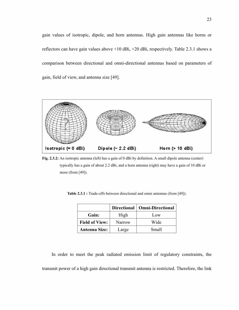
gain values of isotropic, dipole, and horn antennas. High gain antennas like horns or
reflectors can have gain values above +10 dBi, +20 dBi, respectively. Table 2.3.1 shows a
comparison between directional and omni-directional antennas based on parameters of
gain, field of view, and antenna size [49].
Fig. 2.3.2: An isotropic antenna (left) has a gain of 0 dBi by definition. A small dipole antenna (center)
typically has a gain of about 2.2 dBi, and a horn antenna (right) may have a gain of 10 dBi or
more (from [49]).
Table 2.3.1 : Trade-offs between directional and omni antennas (from [49]).
Directional Omni-Directional
Gain: High Low Field of View: Narrow Wide Antenna Size: Large Small
In order to meet the peak radiated emission limit of regulatory constraints, the
transmit power of a high gain directional transmit antenna is restricted. Therefore, the link

24
budget is not directly affected by a high-gain transmit antenna. The only advantage of
high-gain transmit antennas over low-gain transmit antennas might be lower emissions in
undesired directions, which leads to less undesired signals and improved overall system
performance. On the other hand, a high-gain receive antenna plays directly into the link
budget. Typically, those antennas require larger size and higher tolerance of a narrower
field of view [49].
Antennas can be classified as electric or magnetic types. Antennas such as dipoles
and most horns, which are characterized by near-surface intense electric fields, form the
group of electric antennas. In contrast, antennas with near-surface intense magnetic fields
belong to the group of magnetic antennas. Typical examples are loop and slot antennas.
Magnetic antennas are more suitable for embedded systems and related applications
because electric antennas have a higher tendency of producing coupling effects with
surrounding circuitry [49].
2.3.3 Matching and Spectral Control
To design UWB antennas, traditional narrowband methods are often used. However,
modifications and adjustments are required for good designs. As the required bandwidth

25
increases, it becomes more difficult to design a well-matched network between the UWB
antenna and the rest of the system. The purpose of a matching network is to maximize
power transfer and minimize reflections [49].
To design a well-matched network for a UWB antenna, we start with a well-matched
antenna. To obtain a particular impedance for an antenna, the method and the concept are
well understood. A good example would be the microstrip notch antenna designed by
Nester [49]. This antenna is a planar horn antenna that has smooth transitions from a
microstrip to a slotline, and with continuously variable elements. Fig. 2.3.3 illustrates
Nester’s antenna [49].
Fig. 2.3.3: The continuously tapered slot horn
elements of Nester (gray colorization on
elements added) (from [49]).
Fig. 2.3.4: A hypothetical tapered horn antenna (top)
with a transition from 50 Ω to 377 Ω
(bottom) (from [49]).

26
Complex computer algorithms are required to calculate the impedance of a slotline
horn over a wide bandwidth. To demonstrate the idea, a simpler structure can be used.
Consider a cross-sectional width (w) and a height (h) of a parallel-plate horn antenna. The
impedance of an air gap between two plates can be approximated by (c.f. Fig. 2.3.4):
whZZ 0= (2.2)
It is important to know that this result is only exact for w >> 10 h, but it is used here to
give an idea of the order of magnitudes. A 50 Ω match requires h/w ≈ 0.133 while a 377
Ω match requires h/w ≈ 1.00. Another example would be a hypothetical horn antenna
matched to a 50 Ω feed line. The linear transition from 50 Ω to 377 Ω produces a
well-matched network. Then, the long 377 Ω section is tapered to cover ultra-wideband
frequencies. This antenna is illustrated in Fig. 2.3.4 [49].
Desired frequency ranges can be designed into an antenna. One of the simplest ways
is to modify the scale of the same antenna. For example, across a 3:1 frequency range, a
planar elliptical dipole antenna has a value of |S11| in the order of -20 dB. Also, the minor
axis of a planar elliptical dipole antenna is approximately 0.14λ at the lower end of the

27
frequency band. Therefore, the antenna with the frequency band of 1-3 GHz will have
elements of approximately 1.67-inch in its minor axis. A 2-6 GHz antenna will have half
the size (one fourth of the area) of the 1-3 GHz antenna with about 0.83-inch elements;
and a 3-9 GHz antenna has approximately 0.56-inch elements, which will be one third the
size (one ninth of the area) of the original one [49].
By applying more sophisticated methods, an UWB antenna can be made relatively
insensitive to selective frequencies by using frequency notch implementations. Also, to
some extent, the roll-off of he spectral rate at the edges of an operational band can be
controlled. When designing an ultra-wideband system, considerations in all different
angles must be taken into account. In order to make contribution to the whole system, an
UWB antenna must be customized in both its impedance and frequency responses [49].
2.3.4 Directivity and System Performance
Friis Transmission Equation regulates the link characteristic of a narrowband
antenna in free space. It assumes impedance-matched and polarization-matched
conditions.

28
22
2
2
2
)4()4( frcGGP
rGGPP RXTX
TXRXTX
TXRX ππλ
== (2.3)
PRX is the received power, PTX is the transmitted power, GTX is the transmit antenna gain,
GRX is the receive antenna gain, λ is the wavelength, f is the frequency, c is the speed of
light, and r is the distance between the transmit and receive antennas. In the case of an
UWB antenna, Friis Transmission Equation needs to be expressed in terms of spectral
power density; power and gain will be functions of frequency:
22
2 )()()()4(
)(f
fGfGfPr
cfdP RXTXTXRX π
= (2.4)
The total received power can be obtained by taking the integration over frequency:
∫∞
=0
)( dffdPP RXRX (2.5)
The effective isotropic radiated power (EIRP) is:
)()()( fGfPfEIRP TXTX= (2.6)

29
GTX(f) is the peak gain of the antenna in any orientation. The term EIRP is defined by
regulatory limits. System designers intend to get the constant product of PTX(f) GTX(f) as
near to the limit of 3 dB safety margin. In order for the transmit signal to fall within the
limit of the permitted spectral mask, the power gain product will usually need to be
reduced [49].
From equation 2.3, the path loss can be referred to as (λ/4πr)2 or as (c/(4πrf))2
variation of the signal power. The longer the distance r (the larger the 4πr2 surface area),
the greater is the spread of the transmit signal, and the smaller is the signal captured by
the receive antenna. In another way, the signal energy is diffused rather than lost. The
2
1f
dependence in the path loss does not suggest that signals in free space are attenuated
inversely proportional to the square of the frequency. Actually, the definition of antenna
gain and antenna aperture presents the 2
1f
dependence. Antenna gain G(f) is defined in
terms of antenna aperture A(f) as:
2
2
2
)(4)(4)(c
ffAfAfG πλπ
== (2.7)
The antenna aperture is defined by a measure of how large a part of an incoming wave

30
front an antenna can capture. The antenna aperture can be also expressed as the effective
area of the antenna. The antenna aperture tends to be roughly equal to the physical area of
the antenna for electrically large directive antennas. As for small elements and
omni-directional antennas, the antenna’s physical area may actually be significantly
smaller than the antenna aperture. With the ability of electromagnetic waves to couple to
objects within a range of about λ/2π, even a thin wire or a planar antenna can still be an
effective receiver or radiator of electromagnetic radiation [49].
A constant gain antenna has constant aperture in term of wavelength. For example,
the aperture of a dipole antenna is approximately 0.132λ2. The constant gain antenna
aperture decreases with 2
1f
as the frequency increases, or as λ decreases.
Omni-directional antennas are typically modeled to have constant gain and pattern
behavior. On the other hand, an antenna aperture, which remains fixed with frequency, is
described as a constant aperture antenna. Typically, a horn antenna will have a fixed
aperture. The size of the aperture in term of wavelength increases proportional to 2f ,
which narrows the pattern and increases the antenna gain by 2f . Typically, directive
antennas reveal this characteristic [49].

31
Fig. 2.3.5 illustrates free space transmission behaviors of different types of transmit
and receive antennas. For the link of omni to omni, both transmit and receive antennas are
constant gain antennas; this results in a roll-off of 2
1f
within the band for the received
power. As for the omni to directional link, the 2
1f
roll-off is canceled by the gain
variation of 2f from the constant aperture receive antenna, which yields a flat received
power in the band. Depending on the receive antenna gain, the received power can be
significantly larger than the omni antenna transmit power. However, this advantage is
balanced out by a narrower pattern and field-of-view that comes with the increasing gain
of a typical directional antenna. Due to the fact that the transmit power needs to be made
to roll-off as 2
1f
in order to meet the limit of a flat EIRP spectral mask, a directional
antenna, whose gain varies as f 2 on the transmit side of the link, does not improve the
system performance [49].
One of the possible advantages of directive antennas over omni-directional antennas
is that directive antennas have the ability to separate signals coming from specific
directions. With this ability, angles of arrival signals can be known. Further, by
implementing spatial processing techniques to incoming multi-path signal components,
unwanted interfering signals can be eliminated [49].

32
Fig. 2.3.5: The relationship between antenna directivity and link performance for an omni TX to omni RX
(top), an omni TX to directional RX (middle) and a directional TX to directional RX (bottom)
(from [49]).
2.3.5 Antenna Dispersion
Conventionally, gain and return loss (matching) are two fundamental parameters
engineers use when evaluating antennas. Only little variation is permitted over the
operating band for conventional narrowband antennas. Therefore, those parameters are
assumed to be constant. For broadband antennas such as UWB antennas, however, gain

33
and return loss are defined as functions of frequency since they largely vary over a wide
frequency range. Moreover, gain is just a scalar quantity and contains no phase
information. But the performance of UWB antennas does heavily depend on their phase
variation. An UWB antenna will radiate a dispersive and twisted waveform, even though
the gain of the UWB antenna may appear well performed. The reason is that the phase
center of an antenna varies with respect to frequency, or even moves as function of the
observation angle [50].
For those systems, in which the entire operational band is utilized by a single
radiated signal, or even multi-band systems, dispersion is a significant concern.
Compensation is usually required for UWB systems when dispersion problems occur
within the UWB antenna; even though it may be complex and costly. Conventionally,
broadband characteristics can be obtained through physical geometry’s variation for
classical frequency independent antennas. Lower frequency parts of a signal can be
produced by the larger scale portion of the antenna, and high frequency parts by the
smaller portions. Frequency independent antennas will radiate dispersive waveforms,
though, since the phase center varies with respect to the frequency [50].

34
For example, the following Fig. 2.3.6 illustrates a 1 to 11 GHz log spiral antenna.
The antenna is fed at the tip of the cone where the center of the feeding coaxial line is
connected. The smaller scale part of the spiral generates high frequency signals. At the
base of the spiral antenna, where the larger scale part is placed, lower frequency
components radiate. Fig. 2.3.7 illustrates the transmitted and the received signals of this
log spiral antenna. The left side of the figure shows the transmitted impulse voltage signal
detected at the feeding terminal of the transmitted antenna. The right side of the figure
shows the received impulse voltage signal detected at the feeding terminal of the
receiving antenna. From the received signal, the effect of dispersion is clearly revealed.
Two very distinctive behaviors of the received signal expose the dispersive effect. First,
the dispersive characteristic of the antenna causes the received signal to have over twice
the signal length compared to the transmitted signal. Secondly, the dispersive effect is
obvious from the “chirp” in the received signal waveform. Higher frequency components
with narrower zero crossing time periods appear at the beginning part of the received
signal. While lower frequency components with wider zero crossing time periods arrive
later [50].
There is another downside from the dispersive effect, which is not clearly revealed in

35
Fig. 2.3.7. The received signal will change with respect to the observation angle as the
phase center varies with frequency. With non-dispersive UWB antenna elements, much
better system performance can be easier obtained. Therefore, the focus in recent years has
been on small UWB antennas due to their many advantages over the conventional
wideband antennas.
Fig. 2.3.6: Log conical spiral antennas (from [50]).
Fig. 2.3.7: Transmitted (left) and received (right) voltage waveform
from a pair of conical log spiral antennas (from [50]).

36
Planar elliptical dipole antennas are one of the most common small element dipole
antennas used. Flat dipole-like patterns and 3:1 frequency span gains are some of the
featured characteristics of planar elliptical dipole antennas; also, broad bandwidths with
typical return losses of 20 dB or better are obtained. Finally, non-dispersive and compact
radiated waveforms will generally be produced by planar elliptical dipole antennas. A pair
of identical planar elliptical dipole antennas is illustrated in Fig. 2.3.8. The planar
elliptical dipole antenna has a minor axis of 3.8 cm and a major axis of 4.8 cm resulting in
an axial ratio of 1.25:1.
Fig. 2.3.8: 1.25:1 axial ratio planar elliptical dipoles with 4.8x3.8 cm
elements [50].

37
Fig. 2.3.9: Transmitted (left) and received (right) voltage waveform from a pair of
planar elliptical dipole antennas (from [50]).
Fig. 2.3.9 displays the transmitted (left) and received (right) voltage signals from a pair of
planar elliptical dipole antennas. It is obvious that both signals look very similar. This
reveals the non-dispersive behavior of planar elliptical dipole antennas. With minimum
variation in the relative delay between paths of various frequency components, UWB
antennas with very low dispersion are achievable [50].

38
3.0 UWB Printed-Circuit-Board (PCB) Antennas
3.1 Introduction to UWB PCB Antennas
In the recent rapid research of ultra-wideband (UWB) technology, the UWB antenna
is one of the most essential components for an UWB system. Many applications such as
local network, imaging radar, and communication employ UWB technology. Therefore,
developments of UWB antennas become important and complex for system and antenna
designers. In conventional UWB systems, the antenna radiates in the preferred direction
with high gain performance and operates over a broad impedance-matched bandwidth.
One of the examples would be log-periodic antennas; they have broadband
impedance matching and reasonable gain in the desired direction. However, due to their
dispersive properties on broadband waveform radiation, extra compensations and
complexities are required. Another type of broadband antenna would be the TEM horn.
To have lower dispersive rating, bi-conical antennas are a good choice for broadband
systems. Bi-conical antennas have a broadband impedance match and tend to generate
non-dispersive waveforms. However, when applying UWB systems to portable devices,
conventional UWB antennas are not suitable. This is mainly due to their bulky size and

39
directional properties. Monopole and dipole antennas are good options for portable UWB
devices. They have great features such as broadband impedance matching, small size and
omni-directional radiation. However, from a system design point of view, fabrication may
not be easy because those antennas require a perpendicular ground plane. Therefore,
planar or printed-circuit board (PCB) antennas are much more suitable in terms of
manufacturing complexities. Also, when designing UWB antennas, designers must make
new considerations based on new UWB standards.
As for portable applications, PCB antennas are the most suited compared to other
types of UWB antennas. Therefore, different types of planar UWB antennas have been
developed. UWB PCB antennas are usually compact in design and small in size. Also,
planar antennas can be easily designed to have broad bandwidth and omni-directional
radiation. Relatively small planar antennas will tend to generate low-dispersive
waveforms. Most of the planar antennas developed so far are in microstrip or coplanar
waveguide (CPW) technology. Future UWB systems in mobile devices will operate at
high data rate and in short-range applications. Planar antennas are widely used in wireless
communications due to their low cost and light-weight properties as well as their ease of

40
fabrication. Therefore, the realization of UWB antennas in printed-circuit technologies
within relatively small substrate areas is of primary importance.
In the following sections, two primary types of PCB antennas will be compared.
They are designed in microstrip and CPW feeding technologies. Several examples from
both technologies will be selected and compared. The comparison will be based on
antenna performances in five different areas: voltage standing wave ratio (VSWR) or
return loss (S11), gain, radiation patterns, polarization, and group delay or phase center
variation. The first parameter, VSWR, should be less or equal to 2 for the required
bandwidth or the return loss should be less or equal to -10 dB. Those parameters indicate
how well the impedance is matched over the operational bandwidth. The second
parameter is the gain of a UWB antenna. Typically, the gain refers to the maximum gain
for each frequency of the operating band, independent of the varying direction. The third
parameter is the radiation pattern, where directionalities of radiation are determined. Most
of the time, omni-directional radiation patterns are preferable for portable UWB antennas.
The fourth parameter is the polarization of the antenna. Two different and
perpendicular polarizations are defined, both vertical polarization θE (co-polarization)

41
and horizontal polarization φE (cross-polarization). If an antenna’s radiating elements
are parallel located in the y-z plane, perpendicular to the x-axis and facing the positive
x-axis direction, then both polarizations will be oriented as illustrated in Fig. 3.1.1. In
order to completely observe radiation patterns and polarization of an UWB antenna, two
primary perpendicular radiation planes need to be defined, both E-plane and H-plane. For
each plane, both polarizations need to be plotted for selected frequencies. Typically, four
radiation plots will be required, two plots for each plane, and one for each polarization.
With respect to the orientation of Fig. 3.1.1, the x-y plane is defined as H-plane and y-z
plane or x-z plane is defined as E-plane.
Fig. 3.1.1: Orientation of field components, both polarizations.
42
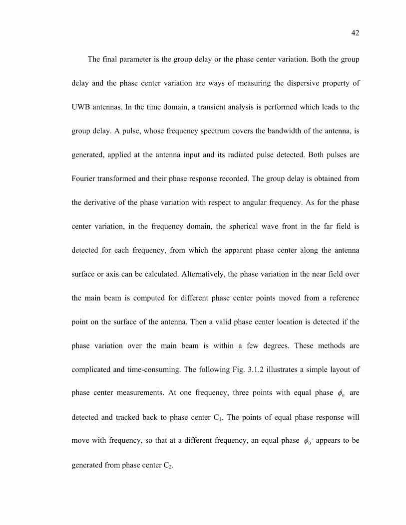
The final parameter is the group delay or the phase center variation. Both the group
delay and the phase center variation are ways of measuring the dispersive property of
UWB antennas. In the time domain, a transient analysis is performed which leads to the
group delay. A pulse, whose frequency spectrum covers the bandwidth of the antenna, is
generated, applied at the antenna input and its radiated pulse detected. Both pulses are
Fourier transformed and their phase response recorded. The group delay is obtained from
the derivative of the phase variation with respect to angular frequency. As for the phase
center variation, in the frequency domain, the spherical wave front in the far field is
detected for each frequency, from which the apparent phase center along the antenna
surface or axis can be calculated. Alternatively, the phase variation in the near field over
the main beam is computed for different phase center points moved from a reference
point on the surface of the antenna. Then a valid phase center location is detected if the
phase variation over the main beam is within a few degrees. These methods are
complicated and time-consuming. The following Fig. 3.1.2 illustrates a simple layout of
phase center measurements. At one frequency, three points with equal phase 0φ are
detected and tracked back to phase center C1. The points of equal phase response will
move with frequency, so that at a different frequency, an equal phase 0φ, appears to be
generated from phase center C2.

43
Fig. 3.1.2: Simple phase center variation measurement
layout (antenna at the bottom).
3.2 Microstrip UWB Antennas
Microstrip technology is one of the most common techniques used to design planar
antennas. However, when microstrip technology is applied to planar UWB antennas,
fabrication on both sides of the substrate is required. This means that microstrip UWB
antennas must have ground planes on the opposite side of the substrate material to support
the feeding microstrip line. Two different designs of microstrip UWB antennas from other
published papers are presented here for comparisons. Those antennas will be illustrated in
terms of those five performance parameters mentioned in the previous section.
44
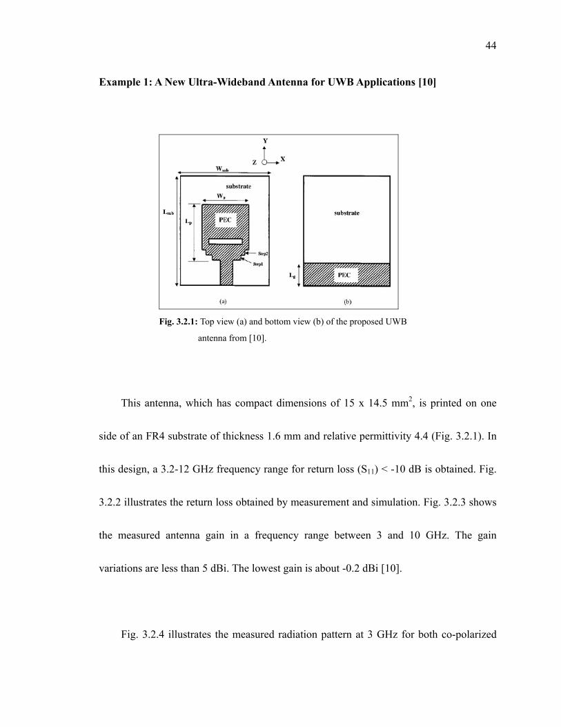
Example 1: A New Ultra-Wideband Antenna for UWB Applications [10]
Fig. 3.2.1: Top view (a) and bottom view (b) of the proposed UWB
antenna from [10].
This antenna, which has compact dimensions of 15 x 14.5 mm2, is printed on one
side of an FR4 substrate of thickness 1.6 mm and relative permittivity 4.4 (Fig. 3.2.1). In
this design, a 3.2-12 GHz frequency range for return loss (S11) < -10 dB is obtained. Fig.
3.2.2 illustrates the return loss obtained by measurement and simulation. Fig. 3.2.3 shows
the measured antenna gain in a frequency range between 3 and 10 GHz. The gain
variations are less than 5 dBi. The lowest gain is about -0.2 dBi [10].
Fig. 3.2.4 illustrates the measured radiation pattern at 3 GHz for both co-polarized

45
and cross-polarized fields. From Fig. 3.2.4, nearly omni-directional radiation pattern is
obtained for the co-polarized radiation in the xz-plane. However, there is too much
variation between the co-polarized and cross-polarized radiation and, therefore wideband
operation in dual polarization is not possible.
Fig. 3.2.2: Return loss in both simulation and measurement from [10].
Fig. 3.2.3: Measured antenna gain from [10].

46
Fig. 3.2.4: Measured radiation patterns at 3 GHz, xy-plane (left) and xz-plane (right) from [10].
Fig. 3.2.5 illustrates the measured group delay. From the figure, group delay variations of
up to 0.5 ns can be observed within the operating bandwidth (2-12 GHz) [10].
Fig. 3.2.5: Measured group delay from [10].

47
Example 2: Low-Cost PCB Antenna for UWB applications [12]
Fig. 3.2.6: Layout of the proposed antenna from [12].
Fig. 3.2.7: Return loss of both simulation and measurement from [12].
Fig. 3.2.8: Measured gain from [12].
This UWB antenna is fabricated on a 3 x 3 cm2, 1.6-mm-thick FR4 board (Fig.

48
3.2.6). Fig. 3.2.7 illustrates the return loss obtained from both simulation and
measurement. The bandwidth covers a frequency range from 3.4 GHz to 11 GHz. Gain
results are displayed in Fig. 3.2.8 between 4 GHz and 10 GHz. The gain variation is about
5 dBi. The lowest gain is about -0.5 dBi at 10 GHz [12] and demonstrates that this
antenna is a very poor radiator at high frequencies.
Fig. 3.2.9: Measured radiation patterns in xz-plane and xy-plane from [12].

49
Fig. 3.2.9 illustrates measured radiation patterns in both the xz- and xy-planes for
various frequencies. Nearly omni-directional radiation patterns are obtained in the
xz-plane. However, no information about polarization is provided in the paper. Fig. 3.2.10
displays the measured group delay. Its variation is less than 100 ps from 3 GHz to 12 GHz
[12].
Fig. 3.2.10: Measured group delay from [12].
3.3 Coplanar Waveguide (CPW) UWB Antennas
Most of the PCB antennas are microstrip-type antenna. They will need a ground
plane on the opposite side of the substrate for electromagnetic waves to travel along the
feed line. However, by applying CPW feed technology, only one side of the substrate
needs to be processed. Both radiating elements and ground planes are on the same side of
the substrate. Therefore, most of the electromagnetic wave travels in the slots on the

50
surface of the substrate, and less energy is lost in the substrate. Thus, this provides a
possibility for a wider impedance matching bandwidth. Also, the CPW feeding technique
requires an easier fabrication process. Two different designs of CPW-fed UWB antennas
from other published papers are presented here to showcase the state-of-the-art. Those
antennas will be illustrated in terms of those five performance areas mentioned in section
3.1.
Example 1: An Ultrawideband Coplanar Waveguide-Fed Tapered Ring Slot Antenna [23]
Fig. 3.3.1: Layout of the proposed UWB antenna, (a) top view and (b)
cross-section view from [23].
51
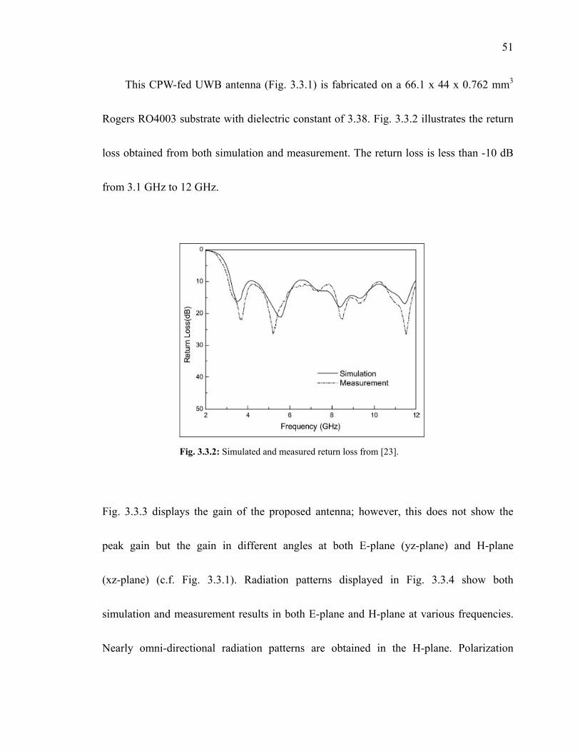
This CPW-fed UWB antenna (Fig. 3.3.1) is fabricated on a 66.1 x 44 x 0.762 mm3
Rogers RO4003 substrate with dielectric constant of 3.38. Fig. 3.3.2 illustrates the return
loss obtained from both simulation and measurement. The return loss is less than -10 dB
from 3.1 GHz to 12 GHz.
Fig. 3.3.2: Simulated and measured return loss from [23].
Fig. 3.3.3 displays the gain of the proposed antenna; however, this does not show the
peak gain but the gain in different angles at both E-plane (yz-plane) and H-plane
(xz-plane) (c.f. Fig. 3.3.1). Radiation patterns displayed in Fig. 3.3.4 show both
simulation and measurement results in both E-plane and H-plane at various frequencies.
Nearly omni-directional radiation patterns are obtained in the H-plane. Polarization

52
properties are not displayed in these radiation patterns. Fig. 3.3.5 illustrates various group
delays at different angles in the E-plane. The maximum group delay variation is about 0.5
ns [23].
Fig. 3.3.3: Measured gain responses of the proposed UWB antenna at θ = -45o, 0o,
45o and 90o in (a) E-plane and (b) H-plane from [23].

53
Fig. 3.3.4: Measured and simulated radiation patterns of the
CPW-fed antenna. (a) E (yz) - plane and (b) H (xz) -
plane from [23].

54
Fig. 3.3.5: Measured group delay at θ = -45o, 0o, 45o and 90o in
E-plane from [23].
Example 2: A Compact UWB Antenna with CPW-Feed [29]
Fig. 3.3.6: Layout of the proposed UWB
antenna, top view and
cross-section view from [29].

55
Fig. 3.3.7: Simulated and measured return loss from [29].
Fig. 3.3.8: Measured antenna peak gain from [29].
This antenna has a size of 15.5 x 17 mm2 (Wsub x Lsub) and is printed on one side of a
FR4 substrate with thickness of 1.6 mm and relative permittivity of 4.4 (Fig. 3.3.6). Fig.
3.3.7 illustrates the return loss obtained from both simulation and measurement. This
antenna has a return loss of less or equal to -10 dB from 3.08 GHz to 10.3 GHz. Fig. 3.3.8
displays the measured peak gain. Gain variations are about 4 dBi, and the lowest gain is
about 2.6 dBi. Radiation patterns are illustrated in Fig. 3.3.9. Both polarizations at various
frequencies are displayed in the xy-, xz- and yz-planes. Nearly omni-directional

56
co-polarized radiation patterns are obtained in the xy-plane. However, too much variation
between the co-polarized and cross-polarized fields occur; therefore, dual-polarization
cannot be utilized. Also, group delay results are not available in this paper [29].
Fig. 3.3.9: Measured radiation patterns of the proposed UWB antenna from [29].

57
3.4 Comparison between Mirostrip and CPW UWB Antennas
From the previous two sections, different designs in both microstrip and CPW-fed
technologies are compared based on the five performance areas of each example. The
following Table 3.1 illustrates the summary of comparison between each of the two
microstrip and CPW-fed UWB antenna examples.
Table 3.4.1: Summary of comparison between microstrip and CPW-fed UWB antenna examples.
Return
Loss ( ≤
-10 dB)
Peak Gain
Variation/Min
imum peak
gain
Radiation
Patterns
Polarization Group
Delay (ps)
Substrate
Area
(mm2)
Microstrip
Example 1
3.2 - 12
GHz
5 dBi/-0.2dBi
Omni-directional
in
co-polarization
Single
polarization
< 500
15 x 14.5
mm2
Microstrip
Example 2
3.4 – 11
GHz
5 dBi/-0.2dBi
Omni-directional
radiation
Not available
< 100
30 x 30
mm2
CPW-fed
Example 1
3.1 - 12
GHz
Cannot
compare
Omni-directional
radiation
Not available
< 500
66.1 x 44
mm2
CPW-fed
Example 2
3.08 –
10.3
GHz
4 dBi/2.6dBi
Omni-directional
in
co-polarization
Single
polarization
Not
available
15.5 x 17
mm2
From Table 3.1, it can be concluded that the CPW-fed technique will give a slightly better
bandwidth depending on the design. Moreover, less peak gain variation and higher
minimum peak gain are achievable.

58
4.0 UWB Coplanar Waveguide Antennas
4.1 The First Design
A new printed-circuit antenna in coplanar waveguide technology for ultra-wideband
applications is introduced in this thesis. Since design guidelines for UWB antennas are
nonexistent, the design of this new CPW UWB PCB antenna starts from the design of
[14]. The layout of this antenna is presented in Fig. 4.1.1, and Fig. 4.1.2 displays its
dimensions. This planar triangular monopole antenna has a VSWR of less than 2.5 from 4
GHz to 10 GHz. Fig. 4.1.3 illustrates the VSWR results. Radiation patterns in the H-plane
(xy-plane) between 4 GHz to 7 GHz are displayed in Fig. 4.1.4. Both polarizations, Eθ
(co-polarization) and EΦ (cross-polarization), are presented. Omni-directional radiation
patterns are obtained the in co-polarization [14].
Fig. 4.1.1: Layout of the antenna from [14].
Fig. 4.1.2: Dimensions of the antenna from [14].
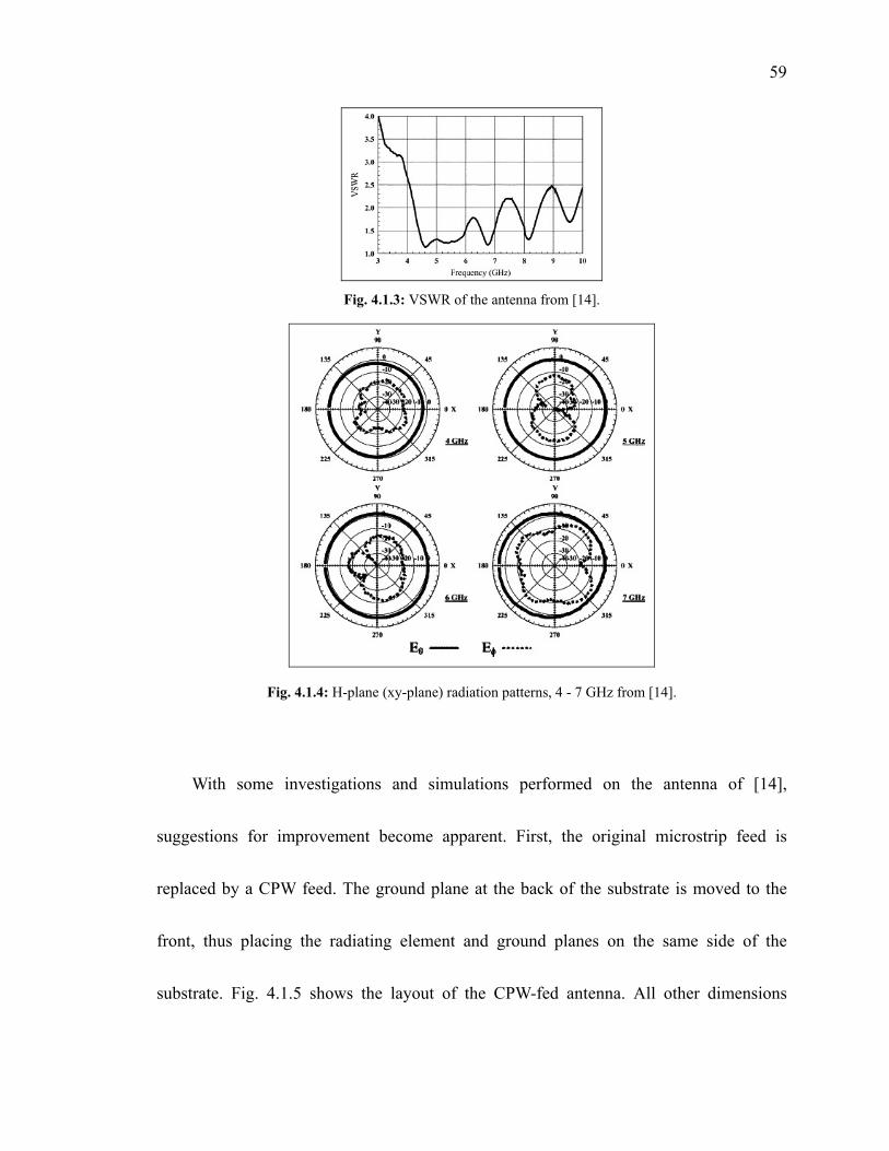
59
Fig. 4.1.3: VSWR of the antenna from [14].
Fig. 4.1.4: H-plane (xy-plane) radiation patterns, 4 - 7 GHz from [14].
With some investigations and simulations performed on the antenna of [14],
suggestions for improvement become apparent. First, the original microstrip feed is
replaced by a CPW feed. The ground plane at the back of the substrate is moved to the
front, thus placing the radiating element and ground planes on the same side of the
substrate. Fig. 4.1.5 shows the layout of the CPW-fed antenna. All other dimensions
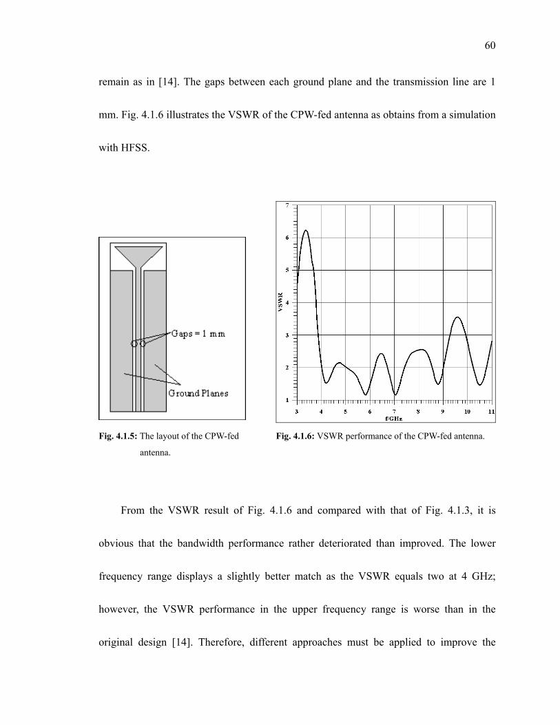
60
remain as in [14]. The gaps between each ground plane and the transmission line are 1
mm. Fig. 4.1.6 illustrates the VSWR of the CPW-fed antenna as obtains from a simulation
with HFSS.
Fig. 4.1.5: The layout of the CPW-fed
antenna.
Fig. 4.1.6: VSWR performance of the CPW-fed antenna.
From the VSWR result of Fig. 4.1.6 and compared with that of Fig. 4.1.3, it is
obvious that the bandwidth performance rather deteriorated than improved. The lower
frequency range displays a slightly better match as the VSWR equals two at 4 GHz;
however, the VSWR performance in the upper frequency range is worse than in the
original design [14]. Therefore, different approaches must be applied to improve the

61
VSWR performance of the CPW-fed antenna. This can include a change in the physical
size of the antenna or in the configuration of the radiating element and the ground planes.
4.2 Different Design Approaches
In order to obtain the operational UWB frequency band (3.1 GHz to 10.6 GHz)
proposed by the FCC, changes must be made to increase the bandwidth. A first approach
is to change the physical size of the antenna. The original antenna dimensions [14] are 20
x 60 mm2 (W x L) (c.f. Fig. 4.1.2). To bring the VSWR down to a value of two for the
lower frequency band (3 GHz to 4 GHz), the physical size of the new antenna design is
adjusted to 30 x 40 mm2 (W x L). Wider width increases the performance in the lower
frequency band. Next, a stepped configuration is introduced to both the radiating patch
and ground planes. Those steps can be viewed as individual resonating elements which
create multiple interacting resonances in the operating band. This follows from basic
principles outlined in [37]. Fig. 4.2.1 illustrates the first design approach. The VSWR
performance of Fig. 4.2.1 as computed by HFSS is displayed in Fig. 4.2.2.
From the VSWR result of Fig. 4.2.2, it is apparent that changing the physical size of
the antenna extends the bandwidth to the lower frequency range.

62
Fig. 4.2.1: Layout of the first design approach. Fig. 4.2.2: VSWR performance of the first design
approach.
In this case, between 3 GHz to 4.4 GHz, VSWR values are now less than two. However,
the stepped configuration in both the radiating patch and ground planes has not yet
improved the overall VSWR performance. Therefore, different stepped configurations
need to be investigated. Fig. 4.2.3 illustrates the second design approach; the only change
made is on the stepped configuration. This time, the opening edges between the radiating
patch and ground planes are increased from 15.5 mm to 17 mm. This produces better
resonances in the lower frequency range. As a result, the stepped configuration of the
radiating patch and ground planes appear somewhat like a conical shape profile. The
VSWR performance for the second design approach is displayed in Fig. 4.2.4. The lower

63
frequency band is improved. A VSWR value ≤ 2 is obtained from 2.9 GHz to 5.9 GHz.
By applying the idea of wider opening edges, further investigations can be made to
extend the operating bandwidth.
Fig. 4.2.3: Layout of the second design
approach.
Fig. 4.2.4: VSWR performance of the second design
approach.
In order to make the opening edges wider, the lengths of ground planes are decreased
from 30 mm to 25 mm. In this way, the distances of the opening edges increase from 17
mm to 27 mm, and the new stepped configuration is applied to resemble a more conical
profile. This third design approach is illustrated in Fig. 4.2.5. Fig. 4.2.6 displays its
VSWR performance. It is obvious that the VSWR improved significantly. It is larger than

64
two only in two narrow ranges, 6.8 GHz to 7.6 GHz and 9.3 GHz to 10.4 GHz.
Fig. 4.2.5: Layout of the third design approach. Fig. 4.2.6: VSWR performance of the third design
approach.
By adjusting the lengths of the opening edges and the step size of each step, further
increases in bandwidth can be achieved. Fig. 4.2.7 illustrates the fourth design approach
with opening edge lengths equal to 24 mm and with larger step size. The VSWR
performance is displayed in Fig. 4.2.8. This time, the higher frequency range, up to 10.3
GHz has a VSWR value of less than two. The design of a new UWB printed-circuit
antenna in coplanar technology is getting closer. Fig. 4.2.9 shows comparisons of VSWR
performance from the first design approach to the fourth design approach.

65
Fig. 4.2.7: Layout of the fourth design approach.
Fig. 4.2.8: VSWR performance of the fourth design
approach.
Fig. 4.2.9: Comparisons of VSWR performances from the first to the fourth design
approaches.

66
4.3 The Final Design
After a variety of design approaches, with some optimization on different step sizes,
a new printed-circuit antenna in coplanar waveguide technology for UWB is introduced.
The frequency of operation is 3.1 GHz to 10.6 GHz with a VSWR < 2. Fig. 4.3.1
illustrates the layout of the new UWB antenna with detailed dimensions, and Table 4.1
displays the dimensional values. This UWB antenna uses an FR4 substrate of 1mm
thickness and 30mm x 40mm (W x L) substrate area. The permittivity parameters are εr =
4.7 and tanδ = 0.018.
Table 4.3.1: Dimensional values of the proposed UWB antenna.
Symbol Distance
(mm) Symbol Distance
(mm) Symbol Distance
(mm) W 30 W8 2 H8 1 L 40 W9 3 L1 2
W1 1 H1 1 L2 3 W2 2 H2 5 L3 2 W3 1.5 H3 3 L4 1 W4 1.5 H4 2 L5 1 W5 1 H5 1 L6 1 W6 1 H6 1 W7 2 H7 1

67
Fig. 4.3.1: Detailed layout of the proposed UWB antenna in CPW technology.
The design of the coplanar UWB antenna follows basic principles outlined in [37] as
far as the stepped configuration in Fig. 4.3.1 is concerned. The slots have been inserted on
a rough trial-and-error basis. Also, the width of the antenna is designed to increase the
lower frequency band. The design of the antenna appears to be a stepped version of a
similar antenna presented in [26]. However, there are two fundamental differences. First
of all, the antenna in [26] is a slot radiator, which maintains metallic strips at the left and
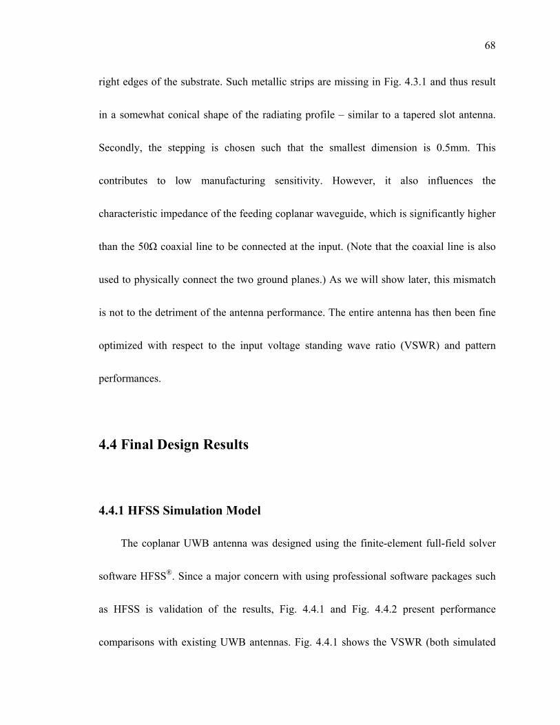
68
right edges of the substrate. Such metallic strips are missing in Fig. 4.3.1 and thus result
in a somewhat conical shape of the radiating profile – similar to a tapered slot antenna.
Secondly, the stepping is chosen such that the smallest dimension is 0.5mm. This
contributes to low manufacturing sensitivity. However, it also influences the
characteristic impedance of the feeding coplanar waveguide, which is significantly higher
than the 50Ω coaxial line to be connected at the input. (Note that the coaxial line is also
used to physically connect the two ground planes.) As we will show later, this mismatch
is not to the detriment of the antenna performance. The entire antenna has then been fine
optimized with respect to the input voltage standing wave ratio (VSWR) and pattern
performances.
4.4 Final Design Results
4.4.1 HFSS Simulation Model
The coplanar UWB antenna was designed using the finite-element full-field solver
software HFSS®. Since a major concern with using professional software packages such
as HFSS is validation of the results, Fig. 4.4.1 and Fig. 4.4.2 present performance
comparisons with existing UWB antennas. Fig. 4.4.1 shows the VSWR (both simulated

69
and measured) of the triangular monopole antenna presented in [14]. Although the
agreement between theory and measurements is not ideal, the simulations agree well with
measurements over the entire 3-10 GHz bandwidth. A similar comparison for the
multiple-resonance UWB antenna presented in [37] is shown in Fig. 4.4.2 for the VSWR
performance and in Fig. 4.4.3 for radiation patterns. Note that this design operates over a
much larger bandwidth than that of Fig. 4.4.1. Nonetheless, the simulated performances
agree well with measurements, thus validating the simulations with HFSS. The
differences between simulated and measured results are attributed by the measurement
setup, which cannot be included in the simulation model. As far as Fig. 4.4.2 is concerned,
both simulated and measured results satisfy the design specification of VSWR ≤ 2.
Fig. 4.4.1: VSWR performance (simulated and measured) of the
UWB antenna presented in [14].

70
Fig. 4.4.2: VSWR performance (simulated and measured) of the
UWB antenna presented in [37].
Fig. 4.4.3: E- and H-plane radiation patterns at 10 GHz (simulated
and measured) of the UWB antenna presented in [37].

71
Fig. 4.4.4 illustrates the final design model created in HFSS. It has three main parts:
UWB antenna, coax cable, and radiation boundary. The UWB antenna consists of the
printed-circuit board, one radiating patch and two ground planes. In the simulation model,
the radiating patch and the two ground planes are just surfaces without thickness; they are
set up to be perfect electric boundaries in HFSS. In order to obtain more accurate
simulation results, finer mesh operations such as surface approximations are applied on
the radiating patch and the two ground planes. The setting for all those surfaces is: surface
deviation = 0.1 mm, normal deviation = 5 deg, and aspect ratio = 4.
Fig. 4.4.4: Final design model of proposed UWB antenna in HFSS.

72
The coax cable part consists of the inner conductor, the dielectric gap and the outer
ground shielding. The inner conductor is modeled as a perfect electric conductor (pec)
material, and has a radius of 0.6 mm. The dielectric gap material is polyethylene and has
εr = 2.25 and tanδ = 0.018. The outer ground shielding is modeled as perfect electric
boundary surface around the dielectric gap. It has a radius of 2.094 mm. Three small
connecting pins are created in the simulation model to connect the inner conductor of the
coax cable to the center conductor of the radiating patch and the outer ground shielding of
the coax cable to the ground planes of the UWB antenna. The length of the coax cable in
the simulation model is set up to be 45 mm. This allows the input port of the coax cable to
be located outside of the radiation boundary. This coax cable essentially models a 50Ω
coaxial (SMA) connector.
As for the last part of the simulation model, the radiation boundary is a tool in HFSS
to simulate far-field radiation patterns. According to setup procedures in HFSS, the
radiation boundary has to be at least a quarter of a wavelength away from the antenna.
Unlike conventional narrow band antenna designs, UWB antennas have very wide
bandwidths; for simulation simplicities, the wavelength at the lowest frequency of the
operating band is selected as it gives the largest radiation boundary. By selecting the

73
wavelength at the lowest frequency, this radiation boundary can fulfill the condition over
the entire operating band. For the final design simulation model, the wavelength at 2 GHz
is selected. A quarter wavelength at 2 GHz is 37.5 mm. The simulation model uses 40 mm
as the distance from the antenna to the radiation boundary.
The solution type of this final design model is set up in the driven mode category.
Under the HFSS simulating environment, a solution frequency is specified which usually
is the center frequency within the operating band (sweep band). During the simulation,
HFSS will perform an accurate calculation based on this solution frequency for the entire
antenna model. For all other frequencies within the operating band, solutions will be
calculated from matrix manipulations and transformations of the result obtained at the
solution frequency. For traditional narrow band antenna designs, the solution frequency
can be selected as the center frequency of the operating band. However, the operating
band of a UWB antenna is very wide; thus the guidelines for narrow band systems do not
apply. Inaccurate simulation results will occur if the solution frequency is not carefully
chosen. Ideally, in order to get accurate results for UWB components, the entire operating
band should be subdivided into many narrow sub-bands. With different solution
frequency setups for different narrow sub-bands, accurate results can be obtained for each

74
narrow sub-band. This is a good approach for getting an accurate simulation result for an
existing UWB antenna. However, it is not a very practical method when designing an
UWB antenna. In order to speed up the design process, only approximated results are
used when designing an UWB antenna.
The problem that causes inaccurate results is related to the mesh cell size of the
simulation model. Due to the wide operating band, wavelengths of propagating modes
can vary significantly. In HFSS, different solution frequencies will give different mesh
sizes; thus longer wavelengths give larger mesh cell sizes and vice versa. A smaller mesh
cell size means finer meshing, which will model the antenna more accurately. For the
proposed final design of the UWB antenna in coplanar waveguide technology, the
operating band is from 3.1 GHz to 10.6 GHz. Therefore, the frequency of 11 GHz is
selected as the solution frequency, and the band is swept between 2 GHz to 11 GHz. The
antenna simulation is modeled based on the 11 GHz mesh cell size, and the simulation
calculates accurately for the frequency of 11 GHz. Any frequency lower than 11 GHz will
have larger mesh cell sizes; thus the mesh cell size at 11 GHz models the antenna
accurately for any lower frequency. Also, additional mesh operations such as surface
approximations are applied on parts which require finer meshing such as the center patch

75
and the ground planes. With those setups, faster design processes and more accurate
solutions of the simulation models are achieved.
Once a reasonable result for the VSWR is obtained for the proposed UWB antenna,
different solution frequencies are applied for conformation tests. The operating band is
divided into different sub-bands with different solution frequencies such as 3 GHz, 4 GHz,
5 GHz, and up to 10 GHz. Each solution frequency setup has a bandwidth of 2 GHz, thus
using sub-bands overlapping by 1 GHz. From those sub-band simulations, the VSWR
result of the proposed UWB antenna in CPW technology under the 11 GHz solution
frequency setup is confirmed to be accurate. Radiation patterns and gains at different
frequencies are obtained from each sub-band simulation result for the purpose of better
accuracy. The average time for each simulation is about 1 hour and 20 minutes, and the
average memory usage is about 1.5 gigabytes for each simulation.
4.4.2 HFSS Simulation Results
Fig. 4.2.5 demonstrates that the VSWR is below 2 between 3 GHz and 5.7 GHz, and
between 6 GHz and 10.7 GHz. The maximum VSWR of 2.03 occurs at 5.83 GHz. Note
that this result includes effects of a coaxial (SMA) connector attached to the input of the

76
coplanar waveguide. Therefore, compared to other UWB printed-circuit designs, this
performance is excellent. Fig. 4.2.6 shows the maximum gain in the frequency range from
3 GHz to 10 GHz. The variation over the frequency range is about 3.6 dBi. This is
significant but compares well with other UWB antennas operating over similar frequency
ranges.
Fig. 4.4.5: VSWR performance of the proposed final design
UWB antenna in coplanar waveguide technology.
Fig. 4.4.6: Maximum gain of the proposed final design UWB
antenna in coplanar waveguide technology.

77
In order to display the radiation patterns, the conventional definition of angles θ and
φ with respect to coordinates x, y, z ( φθ cossin=rx , φθ sinsin=
ry , θcos=
rz ) is used
(c.f. Fig. 4.4.4). The normalized H-plane radiation patterns in the x-y plane are shown in
Fig. 4.4.7 and Fig. 4.4.8. The vertical polarization (Fig. 4.4.7) is mostly omni-directional
up to 8 GHz and starts to deteriorate slightly at 10 GHz. The reception in horizontal
polarization, which is shown in Fig. 4.4.8 and normalized to the same values as in Fig.
4.4.7, is due to the direction of the field in the coplanar feed line. Therefore, these patterns
are almost zero at φ = 0 degrees and φ = 180 degrees. Such property can be used in
polarization sensitive measurements. The co-polarized patterns in the E-plane are shown
in Fig. 4.4.9 (y-z plane) and in Fig. 4.4.10 (x-z plane). It is demonstrated that the basic
shapes of the patterns do not significantly change over the frequency band of operation
and that – as expected – variation is larger towards the upper frequency limit. Also, those
radiation patterns behave like those of dipole antennas. These results compare well with
those of other printed-circuit UWB antennas. Note that in presenting these normalized
radiation patterns, different normalization constants have been used. For example, the
90-degree values in Fig. 4.4.7 and Fig. 4.4.9 should be identical, but they differ by a few
dB due to different normalization.

78
Fig. 4.4.7: Normalized co-polarized H-plane (x-y plane) radiation patterns
Eθ(π/2, φ) of the coplanar UWB antenna for various frequencies.
Fig. 4.4.8: Normalized cross-polarized H-plane (x-y plane) radiation patterns
EΦ(π/2, φ) of the coplanar UWB antenna for various frequencies.

79
Fig. 4.4.9: Normalized co-polarized E-plane (y-z plane) radiation patterns
Eθ(θ,π/2)) of the coplanar UWB antenna for various frequencies.
Fig. 4.4.10: Normalized co-polarized E-plane (x-z plane) radiation patterns
Eθ(θ,0) of the coplanar UWB antenna for various frequencies.

80
The proposed UWB antenna in CPW technology uses an FR4 substrate, which is one
of the most common materials used for printed-circuit boards. Thus manufacturing
complexities and costs are reduced. However, cheaper substrate material comes with
varying permittivity parameters when the operating frequency changes. Therefore, a
sensitivity test based on variations of relative dielectric constant is performed. From the
manufacturer’s specifications, the relative dielectric constant can vary from 4.0 to 4.7.
Three different values (εr = 4.0, 4.4 or 4.7) are selected for the sensitivity test. Fig. 4.4.11
illustrates the related VSWR results.
Fig. 4.4.11: Comparisons of VSWR performance for different relative dielectric
constants.

81
Variations of VSWR with respect to different relative dielectric constants are limited. For
the operating band from 3.1 GHz to 10.6 GHz, the VSWR values from the three different
relative dielectric constants are mostly below two. The highest VSWR value of 2.1 occurs
around 7.4 GHz for the relative dielectric constant of 4.0. Again, note that those results
include effects of a coaxial (SMA) connector attached to the input of the coplanar
waveguide. Therefore, compared to other UWB printed-circuit designs, those
performances are still excellent.
4.4.3 MEFiSTo-3D Simulation Model
The Transmission-Line Matrix (TLM) method in the time domain is utilized to
determine the group delay of this UWB antenna. In order to compare results obtained for
the proposed coplanar UWB antenna with those of different antennas, the above
time-domain method is also applied to the microstrip UWB antenna presented in [15].
The TLM time-domain field solver MEFiSTo-3D® is used for this task. Fig. 4.4.12 shows
VSWR results of the proposed UWB antenna obtained from both simulation packages,
HFSS and MEFiSTo-3D. Note that the connection of the input of the antenna to a coaxial
cable is included in both simulation models. Good agreement is observed, thus verifying
the antenna’s performance at its input terminal. The only difference is in the higher

82
frequency range, 8.5 GHz to 10.6 GHz, where the VSWR values from MEFiSTo-3D are
slightly higher than two. This is caused by the size limitation of the absorbing boundary
in MEFiSTo-3D. A more detailed description will be presented later in this section.
Fig. 4.4.13 shows VSWR results of the UWB antenna in [15] from both simulation
packages, HFSS and MEFiSTo-3D, and also from the measurements in [15]. The data
from HFSS is in reasonable agreement with measurements. Note that the HFSS model
includes the connection to a coaxial cable. In order to reduce the computational domain,
i.e., shorten the long microstrip feed line shown in [15], the coaxial connector could not
be modeled in MEFiSTo-3D. Therefore, and especially in the higher frequency range, the
agreement between measurements and MEFiSTo-3D is not as good as that with HFSS.
However, the basic shape and the reasonably small discrepancies validate numerical
computations.
Fig. 4.4.14 shows the setup of the simulation model of the proposed UWB antenna
in MEFiSTo-3D. Since the problem is symmetric with respect to a magnetic wall in the
x-z plane (all other walls are absorbing boundaries), only half of the computational space
is required.
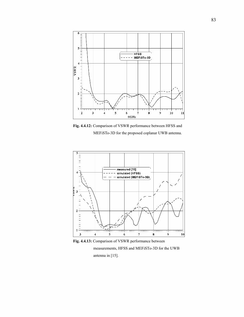
83
Fig. 4.4.12: Comparison of VSWR performance between HFSS and
MEFiSTo-3D for the proposed coplanar UWB antenna.
Fig. 4.4.13: Comparison of VSWR performance between
measurements, HFSS and MEFiSTo-3D for the UWB
antenna in [15].

84
Fig. 4.4.14: Final design model of proposed UWB antenna in MEFiSTo-3D.
In order to observe proper radiating time domain signals, radiating signals need to be
sampled at a distance in the far field. Equation (4.1) presents the minimum distance of the
far field for conventional narrow band antennas. R is the minimum distance from the
center of the radiating source to the far field region at a specific wavelength λ. D is the
largest dimension of the antenna.
λ
22DR = (4.1)

85
However, unlike conventional narrow band antennas, UWB antennas radiate a wide band
of frequencies (wavelengths). Therefore, in order to satisfy the far field condition for the
entire operating band, the longest distance according to equation (4.1) must be used.
For the proposed UWB antenna, the largest dimension is 50 mm (diagonal distance
of a 30 x 40 mm2 PCB). The frequency of 11 GHz is selected as the highest operating
frequency and gives a wavelength of 27.3 mm. By using equation (4.1), the longest far
field distance is about 183.2 mm. Under the environment of MEFiSTo-3D, an absorbing
boundary is required to surround any radiating source, such as an antenna. However, the
absorbing boundary model provided by MEFiSTo-3D is not perfect and thus, some small
reflections will occur. In order to limit the amount of reflections from the absorbing
boundary, the absorbing boundary needs to be in the far field region.
Even though the simulation model makes use of the magnetic wall to half the
computational space, lack of computer memory (RAM – Random Access Memory) is still
a big issue. Microsoft Window XP (32-bit) limits each of its application memory usage to
about 2 gigabytes of RAM. MEFiSTo-3D is a 32-bit application software, which can use
up to 4 gigabytes of RAM. In order to use the full potential of MEFiSTo-3D, Microsoft

86
Window XP (64-bit) is used as the operating system. During the setup of the simulation
model under MEFiSTo-3D, the mesh cell size needs to be selected properly. For the
proposed UWB antenna in CPW technology, the smallest dimension is 0.5 mm. Thus the
selected mesh cell has the volume of 0.5 x 0.5 x 0.5 mm3. Different mesh cell sizes will
require different amounts of computational memory and time; a smaller mesh cell
requires larger RAM and longer simulation time. Even with the amount of RAM available
for the simulation (up to 4 gigabytes), memory is still not sufficient for the full far field
simulation (including the magnetic wall). Only one direction (y-axis) of the absorbing
boundary reaches the far field region, where detecting probes are placed. The origin of the
coordinate system for the simulation model in Fig. 4.4.14 is positioned at the top of the
coaxial input port, which is 20 mm long. The absorbing boundary has the following
dimensions: ∆x = 210 mm (from -105 to 105 mm), ∆y = 185 mm (from 0 to 185 mm) and
∆z = 150 mm (from -20 to 130 mm).
The input of the UWB antenna is excited with a pulse covering the entire frequency
spectrum of the application (3.1 GHz to 10.6 GHz). At a point in the far field, probes
detect the vertical polarization Eθ and the horizontal polarization Eφ. Several detecting
probes are placed closed to the far field boundary (c.f. Fig. 4.4.14). They have the same x

87
and z position (x = 0 mm and z = 26 mm) and along the y direction from 176 mm to
185mm. Some are in positions slightly below the far field boundary and some are in the
far field region. Note that a reference port is included and positioned outside the
absorbing boundary (c.f. Fig. 4.4.14). The purpose of having an extra identical coaxial
input port such as a reference port is to observe undistorted input signals and obtain
proper VSWR performance of the proposed UWB antenna.
With only one direction of the computational boundary actually extending into the
far field region, the VSWR performance of the UWB antenna modeled by MEFiSTo-3D
shows slightly worse results in the higher frequency region. More reflections occur at
higher frequencies due to the size limitation of the absorbing boundary. Higher
frequencies require larger absorbing boundaries in order to reach far field conditions.
Also, due to the mesh cell size, the coaxial input port and the reference port are modeled
differently. The 50 Ohm coax cable has an inner core radius of 0.6 mm and an outer core
radius of 2.094 mm. Due to the mesh cell size, it has to be remodeled to have inner and
outer core radii of 0.5 mm and 2 mm, respectively. This changes the impedance of the
original coax cable to 55 Ohms. With the mismatch at the input, the VSWR performance
of the UWB antenna simulated by MEFiSTo-3D is expected to have some distortion. The

88
average simulation time is about 15 hours, and the average memory usage is about 3.7
gigabytes of RAM.
4.4.4 MEFiSTo-3D Simulation Results
One set of detecting probes is set up in the far field region (x =0 mm, y = 185 mm, z
= 26 mm). Input and detected time domain signals are Fourier transformed to obtain
amplitude and phase responses. The group delay is obtained from the derivative of the
phase response (phase differences between input and detected signals) with respect to
frequency. Fig. 4.4.15 shows the input time-domain signal together with its corresponding
amplitude (in dB) and phase spectrum. Note that the duration of the pulse is about 0.4 ns
and the phase variation is in the order of hundreds of degrees. The radiated signals Eθ
(solid lines) and Eφ (dashed lines) as detected by far field probes in Fig. 4.4.14 and their
amplitude and phase spectra are shown in Fig. 4.4.16. Figs. 4.4.16a and 4.4.16b confirm
that the main polarization is vertical (Eθ) since the detected signal in horizontal
polarization (Eφ) is at least 20 dB below its vertical component. Fig. 4.4.16c shows the
phase variation now in thousands of degrees, which is a result of the ringing of the
detected time signal in Fig. 4.4.16a.

89
(a)
(b)
(c)
Fig. 4.4.15: Time-domain signal (a), amplitude spectrum (b) and
phase spectrum (c) at the input of the coaxial cable
feeding the coplanar antenna (c.f. Fig. 4.4.14).

90
(a)
(b)
(c)
Fig. 4.4.16: Radiated time-domain signal (a), amplitude spectrum
(b) and phase spectrum (c) detected by the probes; Eθ
(solid lines) and Eφ (dashed lines).

91
(a)
(b)
(c)
Fig. 4.4.17: Radiated Eθ time-domain signal (a), amplitude
spectrum (b) and phase spectrum (c) detected by two
sets of probes at the far field boundary (solid lines) and
slightly within the far field boundary (dashed lines).
92
Moreover, notice that the main part of the received pulse in Fig. 4.4.16a looks similar to a
negative derivative of the input pulse rather than the original input signal in Fig. 4.4.15a.
Such behavior is common in antennas that radiate pulses covering a significant frequency
spectrum, e.g. [41].
For the purpose of comparison, main polarization (Eθ) results obtained from two
different sets of detecting probes are illustrated in Fig. 4.4.17. One set of detecting probes
is at the far field boundary (x =0 mm, y = 185 mm, z = 26 mm), and the other set is
slightly inside the far field boundary (x =0 mm, y = 176 mm, z = 26 mm). Note that the
far field boundary is at y = 183.2 mm. As expected, the time domain signal inside the far
field boundary leads that at the far field boundary. From Fig. 4.4.17a and Fig. 4.4.17b,
only little variations between two sets of detecting probes in both amplitude and phase
spectra are observed. Fig. 4.4.18a and Fig. 4.4.18b show the amplitude and group-delay
responses, respectively, of the coplanar UWB antenna fed by a coaxial cable. The
amplitude response in the main polarization (solid line) is between –40 to –50 dB which
is due to the small effective area of the receiving probes. Since the variations in amplitude
and phase (group delay) determine the distortion of the pulse transmitted by the antenna,
the respective values – as read from the data plotted in Fig. 4.4.18 – are summarized

93
below for both vertical (VP) and horizontal (HP) polarizations.
Frequency range: 3.1 GHz – 10.6 GHz
Amplitude variation: < 8.7 db (VP); < 23 dB (HP)
Group-delay variation: < 163 ps (VP); < 620 ps (HP)
Note that the amplitude variation of 8.7 dB in vertical polarization (Eθ) is in very
good agreement with the radiation patterns displayed in Fig. 4.4.9 for individual
frequencies between 3 GHz and 10 GHz. Since Fig. 4.4.18 was obtained from data
computed by the time-domain solver MEFiSTo-3D and Fig. 4.4.9 from that of the
frequency-domain package HFSS, this agreement (together with Fig. 4.4.12) verifies the
design and performance of the proposed coplanar UWB antenna. For comparison
purposes, the microstrip UWB antenna in [15] is also simulated using MEFiSTo-3D to
compute the group delay. After exciting the microstrip antenna with a pulse shown in Fig.
4.4.15, detecting the radiated signal and calculating amplitude and phase responses, the
data presented in Fig. 4.4.19 is obtained. Between 3 GHz and 10 GHz, the amplitude
variation in vertical polarization is similar to that of the coplanar UWB antenna in Fig.
4.4.18a.

94
(a)
(b)
Fig. 4.4.18: Amplitude response (a) and group-delay characteristic (b) of
coplanar UWB antenna; vertical polarization Eθ (solid lines,) and
horizontal polarization Eφ (dashed lines).
The signal level difference between horizontal and vertical polarizations in Fig. 4.4.19a is
smaller than that in Fig. 4.4.18a. This is due to the fact that the x-component of the

95
electric field represents the main polarization in a microstrip line if the antenna is oriented
in the same way as the coplanar one in Fig. 4.4.14. The group delay performances of the
microstrip antenna are inferior to those of the coplanar antenna in both polarizations. The
following values are obtained:
Frequency range: 3.0 GHz – 10.0 GHz
Amplitude variation: < 8.8 db (VP); < 31 dB (HP)
Group-delay variation: < 239 ps (VP); < 1.9 ns (HP)
Both the coplanar and the microstrip antenna display nearly omni-directional
radiation patterns with characteristics slightly distorting towards 10 GHz (c.f. [14] and
[15] for details). Over the 3.1 – 10.6 GHz range, the VSWR performance of the coplanar
antenna is superior to that of the microstrip antenna. The amplitude variations in vertical
polarization are comparable; in horizontal polarization, however, it is 8 dB in favour of
the coplanar antenna. The group-delay variations of the coplanar antenna are much
smaller than those of the microstrip antenna and, therefore, the coplanar structure of Fig.
4.3.1 is better suited for UWB applications.

96
(a)
(b) Fig. 4.4.19: Amplitude response (a) and group-delay characteristic (b) of the
microstrip UWB antenna in [15]; vertical polarization Eθ (solid
lines,) and horizontal polarization Eφ (dashed lines).
It is noted that a smaller group-delay variation (< 100 ps) is reported in [12] for a
microstrip UWB antenna with two slots in the radiating patch. However, the gain of that
antenna is lower than the one reported in Fig. 4.4.6 and even drops below 0 dB above 9.8
GHz [12].

97
4.5 The Improved Final Design
Further improvement can be made on the proposed final design of the UWB antenna
in CPW technology. The coplanar waveguide at the input of the proposed UWB antenna
has an input impedance about 75 Ohm. As mention in Section 4.3, even with the
mismatch between the input of the antenna and the 50 Ohm coaxial line, good VSWR
performance is still obtained. Recall that this relates to the assumed manufacturing
sensitivity which dictates a minimum slot width of 0.5 mm. If higher manufacturing
sensitivity is allowed, a 50 Ohm CPW feed can be designed to match the 50 Ohm coaxial
cable. This section presents an improved UWB antenna design with a 50 Ohm CPW feed.
Only a few changes are made to the originally proposed UWB antenna. Referring to Fig.
4.3.1, W6 is reduced to 0.25 mm and W7 is extended to 2.75 mm. For manufacturing
simplicity, the thickness of the PCB is changed to 1.575 mm instead of 1 mm. The
remaining dimensions are the same. This improved UWB antenna still uses an FR4
substrate PCB and 30mm x 40mm (W x L) substrate area. The permittivity parameters are
εr = 4.7 and tanδ = 0.018.
Fig. 4.5.1 displays VSWR performances obtained from both HFSS and
MEFiSTo-3D, and both simulation results agree well. The values of the improved design

98
are much better than those of the original proposed design (at least a drop of 0.4 in
VSWR in the operating band). The results of the sensitivity test from different relative
dielectric constants are illustrated in the Fig. 4.5.2. Again, only very little variation is
observed. Fig. 4.5.3 shows the gain results of the improved UWB antenna. The variation
is about 3 dBi, which is slightly better than the original design. Radiation patterns are
illustrated from Fig. 4.5.4 to Fig. 4.5.7. Behaviors and characteristics are very similar to
those of the original one, which is due to the fact that the shape and size of the radiating
elements are the same and that only the feed and substrate thickness are altered.
Fig. 4.5.1: Comparison of VSWR performances obtained with HFSS
and MEFiSTo-3D for the improved coplanar UWB
antenna.

99
Fig. 4.5.2: Comparison of VSWR performances for different relative
dielectric constants of the improved UWB antenna design.
Fig. 4.5.3: Maximum gain of the improved UWB antenna in coplanar
waveguide technology.

100
Fig. 4.5.4: Normalized co-polarized H-plane (x-y plane) radiation
patterns Eθ(π/2, φ) of the improved coplanar UWB antenna
for various frequencies.
Fig. 4.5.5: Normalized cross-polarized H-plane (x-y plane) radiation
patterns Eφ (π/2, φ) of the improved coplanar UWB antenna
for various frequencies.

101
Fig. 4.5.6: Normalized co-polarized E-plane (y-z plane) radiation
patterns Eθ(θ,π/2)) of the improved coplanar UWB antenna
for various frequencies.
Fig. 4.5.7: Normalized co-polarized E-plane (x-z plane) radiation
patterns Eθ(θ,0) of the improved coplanar UWB antenna for
various frequencies.

102
(a)
(b) Fig. 4.5.8: Amplitude response (a) and group-delay characteristic (b) of the
improved coplanar UWB antenna; vertical polarization Eθ (solid
lines,) and horizontal polarization Eφ (dashed lines).
Fig. 4.5.8a and Fig. 4.5.8b show the amplitude and group-delay responses,

103
respectively, of the improved coplanar UWB antenna fed by a coaxial cable. In order to
simulate the improved UWB antenna design in MEFiSTo-3D, 0.25 x 0.25 x 0.25 mm3
mesh cells must be used. Due to the memory (RAM) limitation, a much smaller absorbing
boundary is used. This affects both amplitude and group-delay responses. Therefore,
worse results are obtained for both amplitude and group delay variations. However, the
group-delay variation of the principal polarization is only 16 ps above that of the original
design. Compared to Fig. 4.4.18, the results for vertical (VP) and horizontal (HP)
polarizations are:
Frequency range: 3.1 GHz – 10.6 GHz
Amplitude variation: < 22.5 db (VP); < 40.1 dB (HP)
Group-delay variation: < 179 ps (VP); < 1.5 ns (HP)

104
5.0 Conclusions and Further Work
5.1 Conclusions
In the recent rapid research of ultra-wideband (UWB) technology, the UWB antenna
is one of the most essential components. As for mobile applications, printed-circuit
antennas are more suited than other types of UWB antennas. Therefore, different types of
planar UWB antennas have been presented. In this thesis, two types of printed-circuit
antennas in microstrip and coplanar technology are compared based on different design
parameters. Designs in microstrip technology require processing on both substrate sides
for fabrication. However, by applying coplanar technology, a number of advantages for
the fabrication and better antenna performance can be offered.
As the result of the research, the proposed ultra-wideband printed-circuit antenna in
coplanar waveguide technology presents a viable option for communication and
measurements in the 3.1 - 10.6 GHz frequency range. Nearly omni-directional
characteristic is obtained for vertical polarization while the horizontal polarization shows
possible applications for direction finding (nulling). The antenna shows excellent VSWR
characteristics, and the radiation patterns vary within acceptable margins over the entire

105
frequency range. Also, due to variations of the relative dielectric constant in the PCB,
VSWR performances of antennas using different relative dielectric constants are
compared and are found to show little variation. The antenna is designed using a
commercially available electromagnetic field solver, HFSS, which is verified through
measurements at similar ultra-wideband antennas.
Time-domain techniques, applied here in form of the TLM solver MEFiSTo-3D,
present a viable option for the analysis and modeling of UWB printed-circuit antennas.
Amplitude characteristics and VSWR performances extracted from the time-domain
solution agree well with frequency-domain methods, which are used for the design of
UWB antennas. The computation of group-delay data in an actual application of pulsed
transmission is one of the clear advantages of time-domain over frequency-domain
techniques. Even with the computer memory (RAM) limitations encountered, reasonable
group delay results are obtainable. This is considered a simpler way of obtaining group
delay characteristics for UWB antennas than the computation of a varying phase center.
The time-domain modeling procedure presented here is applied to two different
printed-circuit UWB antennas, and agreement with frequency domain computations and
measurements is demonstrated. Comparing different design parameter results, the
106
proposed coplanar UWB antenna not only offers advantages in fabrication over the
microstrip UWB antenna [14], but also has overall better antenna performances. This
makes the proposed coplanar UWB antenna more suitable for UWB applications.
Finally, an improved design of the proposed coplanar UWB antenna is presented. By
changing the input impedance of the CPW feed to 50 Ohm, which matches the 50 Ohm
coaxial cable, better VSWR performance is obtained. Moreover, the maximum gain
variation decreases. While the radiation patterns for various frequencies remain similar to
those of the previous design. Group delay characteristics and amplitude variations slightly
degrade. However, this appears to be mainly due to the much smaller absorbing boundary
used in MEFiSTo-3D, which affects greatly the group delay and amplitude responses.
5.2 Further Work
The proposed coplanar UWB antenna presented in this thesis is not truly ideal for
mobile applications like cellular phones. Ideal cellular phone antennas should be able to
transmit and receive in dual polarizations. In order to be fully operational in any position
or orientation of cellular phones, antennas should have omni-directional radiation patters
in both polarizations. Therefore, the objective for future work is to develop an

107
omni-directional UWB antenna operating in dual polarization. This can be accomplished,
for instance by using two coplanar UWB antennas presented in this thesis and combining
them perpendicularly at their feeds. In this way, the new UWB antenna can produce
omni-directional vertical polarization radiation patterns in the H-plane and
omni-directional horizontal polarization radiation patterns in the E-plane.
Another goal is to reduce the size of the new UWB antenna, which will fit better on
cellular phones considering the limitations of available space. UWB systems have to
coexist with current narrowband applications. Rather than using additional filters to
eliminate such frequencies from the UWB signal, an evolving trend is to investigate
UWB trend antennas with notch characteristics in the respective frequency band. This
might be accomplished by using resonating slots in the radiating patches in order to
develop frequency-dependent mismatches within the feed lines. For future designs
utilizing optimization, a sensitivity analysis of all parameters should be performed in
order to identify those parameters which show the highest influence on the design. This
will reduce design time frames and optimization complexity. Moreover, it will define
manufacturing tolerances.

108
References [1] R.T. Johnk, D.R. Novotny, C.M. Weil, M. Taylor and T.J. O’Hara, “Efficient and
accurate testing of an EMC compliance chamber using an ultrawideband measurement system,” 2001 IEEE EMC-S Int. EMC Symp. Dig., Vol. 1, pp. 302-307, Aug. 2001.
[2] K.W. Jin, T.J. Huat, T.Y.K. Roland, K.C.H. Ernest, “Time-domain measurements of
transient field coupling through slots,” Proc. 17th Int. Zurich Symp. EMC, pp. 642-645, Feb./Mar. 2006.
[3] R.F. Martin, “Ultra-wideband (UWB) rules and design compliance issues,” 2003
IEEE EMC-S Int. EMC Symp. Dig., Vol. 1, pp. 92-96, Aug. 2003. [4] J.D. Brunett, R.M. Ringler and V.V. Liepa, “On measurements for EIRP compliance
of UWB devices,” 2005 IEEE EMC-S Int. EMC Symp. Dig., Vol. 2. pp. 473-476, Aug. 2005.
[5] K. Chung, S. Pyun and J. Choi, “Design of an ultrawide-band TEM horn antenna
with a microstrip-type balun,” IEEE Trans. Antennas Propogat, Vol. 53, pp. 3410-3413, Oct. 2005.
[6] L. Yang and G.B. Giannakis, “Ultra-wideband communications: an idea whose time
has come,” IEEE Signal Proc. Mag., Vol. 21, pp.26-54, Nov. 2004. [7] International Telecommunication Union, Radiocommunication Study Groups,
“Framework for the introduction of devices using ultra-wideband technology,” Document 1/85(Rev.1)-E, 09 Nov. 2005.
[8] K. Kiminami, A. Hirata and T. Shiozawa, “Double-sided printed bow-tie antenna
for UWB communications,” IEEE Antennas Wireless Propagat. Lett., Vol. 3, pp. 152-153, 2004.
[9] J. Liang, C.C. Chiau, X. Chen and C.G. Parini, “Printed circular disc monopole
antenna for ultra-wideband applications,” IEE Electronics Lett., Vol. 40, No. 20, pp.
109
1246- 1247, Sep. 2004. [10] S.H. Choi, J.K. Park, S.K. Kim and J.Y. Park, “A new ultra-wideband antenna for
UWB applications,” Microwave Opt. Technol. Lett., Vol. 40, No. 5, pp. 399-401, Mar. 2004.
[11] J. Liang, C.C. Chiau, X. Chen and C.G. Parini, “Study of a printed circular disc
monopole antenna for UWB systems,” IEEE Trans Antennas Propagat., Vol. 53, pp. 3500-3504, Nov. 2005.
[12] Z.N. Low, J.H. Cheong and C.L. Law, “Low-cost PCB antenna for UWB
applications,” IEEE Antennas Wireless Propagat. Lett., Vol. 4, pp. 237-239, 2005. [13] J. Liang, C.C. Chiau, X. Chen, and C.G. Parini, “Printed circular ring monopole
antennas,” Microwave Opt. Technol. Lett., Vol. 45, No. 5, pp. 372-375, June 2005. [14] C.-C. Lin, Y.-C. Kan, L.-C. Kuo and H.-R. Chuang, “A planar triangular monopole
antenna for UWB communication,” IEEE Microwave Wireless Comp. Lett., Vol. 15, pp. 624-626, Oct 2005.
[15] H.R. Chuang, C.C. Lin and Y.C. Kan, “A printed UWB triangular monopole
antenna,” Microwave J., Vol. 49, pp. 108-120, Jan. 2006. [16] K. Rambabu, M.Z. Alam and J. Bornemann, “Design of compact dual-polarized
printed-circuit antenna for ultra-wideband applications,” Proc. 36th European Microwave Conf., pp. 626-629, Manchester, UK, Sep. 2006.
[17] D.-C. Chang, J.-C. Liu, and M.-Y. Liu, “A novel tulip-shaped monopole antenna for
UWB applications,” Microwave Opt. Technol. Lett., Vol. 48, No. 2, pp. 307-312, Feb. 2006.
[18] C.-F. Tseng and C.-L. Huang, “Ultrawideband planar microstrip-fed monopole
antenna,” Microwave Opt. Technol. Lett., Vol. 49, No. 1, pp. 183-185, Jan. 2007. [19] A. M. Abbosh, M.E. Bialkowski, M.V. Jacob and J. Mazierska, “Investigations into
an LTCC based ultra wideband antenna,” Proc. Asia-Pacific Microwave Conf., 4p.,
110
Suzhou, China, Dec. 2005. [20] C.T.H. Lim, “A GCPW-fed printed antenna for UWB applications,” Proc.
Asia-Pacific Microwave Conf., 3p., Suzhou, China, Dec. 2005. [21] X. Chen, J. Liang, P. Li, L. Guo, C.C. Chiau and C.G. Parini, “Planar UWB
monopole antennas,” Proc. Asia-Pacific Microwave Conf., 4p., Suzhou, China, Dec. 2005.
[22] H.K. Lee, J.K. Park and J.N. Lee, “Design of a planar half-circle shaped UWB
notch antenna,” Microwave Opt. Technol. Lett., Vol 47, No. 1, pp. 9-11, Oct. 2005. [23] T.-G. Ma and C.-H. Tseng, “An ultrawideband coplanar waveguide-fed tapered ring
slot antenna,” IEEE Trans. Antennas Propagat., Vol. 54, pp. 1105-1110, Apr. 2006. [24] Y.-C. Lee, S.-C. Lin and J.-S. Sun, “CPW-fed UWB slot antenna,” Proc.
Asia-Pacific Microwave Conf., 4p., Yokohama, Japan, Dec. 2006. [25] S. Nikolaou, D.E. Anagnostou, G.E. Ponchak, M.M. Tentzeris and J.
Papapolymerou, “Compact Ultra Wide-Band (UWB) CPW-fed elliptical monopole on Liquid Crystal Polymer (LCP),” IEEE AP-S Int. Symp. Dig., pp. 4657-4660, Albuquerque, USA, July 2006.
[26] E.S. Angelopoulos, A.Z. Anastopoulos and D.I. Kaklamani, “Ultra-wideband
bow-tie slot antenna fed by a cpw-to-cpw transition loaded with inductively coupled slots,” Microwave Opt. Technol. Lett., Vol. 48, No. 9, pp. 1816-1820, Sep. 2006.
[27] X.-L. Liang, S.-S. Zhong and W. Wang, “UWB printed circular monopole antenna,”
Microwave Opt. Technol. Lett., Vol. 48, No. 8, pp. 1532-1534, Aug. 2006. [28] J.-S. Sun, Y.-C. Lee and S.-C. Lin, “New design of a CPW-fed ultrawideband slot
antenna,” Microwave Opt. Technol. Lett., Vol. 49, No. 3, pp. 561-564, Mar. 2007. [29] D.-B. Lin, I.-T. Tang and M.-Y. Tsou, “A compact UWB antenna with CPW-feed,”
Microwave Opt. Technol. Lett., Vol. 49, No. 3, pp. 564-567, Mar. 2007.

111
[30] R. Chair, A.A. Kishk and K.F. Lee, “Ultrawide-band coplanar waveguide-fed rectangular slot antenna,” IEEE Antennas Wireless Propagat. Lett., Vol. 3, pp. 227-229, No. 1, 2004.
[31] N. Fortino, G. Kossiavas, J.Y. Dauvignac and R. Staraj, “Novel antennas for
ultrawideband communications,” Microwave Opt. Technol. Lett., Vol 41, No. 3, pp. 166-169 , May 2004.
[32] W. Wang, S.S. Zhong and S.-B. Chen, “A novel wideband coplanar-fed monopole
antenna,” Microwave Opt. Technol. Lett., Vol 43, No. 1, pp. 50-52 , Oct. 2004. [33] J.I. Kim and Y. Jee, “Design of ultrawideband coplanar waveguide-fed LI-shape
planar monopole antennas,” IEEE Antennas Wireless Propagat. Lett., Vol. 6, pp. 383-387, 2007.
[34] C.T.H. Lim, “A GCPW-fed printed antenna for UWB applications,” Proc.
Asia-Pacific Microwave Conf., 3p., Suzhou, China, Dec. 2005. [35] Z.N. Chen and X. Qing, “Research and development of planar UWB antennas,”
Proc. Asia-Pacific Microwave Conf., 4p., Suzhou, China, Dec. 2005. [36] B.L. Ooi, G. Zhao, M.S. Leong, K.M. Chua and C.W.L. Albert, “Wideband LTCC
CPW-fed two-layered monopole antenna,” IEE Electronics Lett., Vol. 41, No. 16, pp. 9-10, Aug. 2005.
[37] K. Rambabu, H.A. Thiart, J. Bornemann and S.Y. Yu, “Ultrawideband
printed-circuit antenna,” IEEE Trans. Antennas Propagat., Vol. 54, pp. 3908-3911, Dec. 2006.
[38] Z. Ying and J. Andersson, “An ultra wideband ‘cobra’ patch antenna,” IEE
Proc.-Microw. Antennas Propag., Vol. 151, pp. 486-490, Dec. 2004. [39] Multispectral Solutions, Inc., “Ultra Wideband (UWB) Frequently Asked Questions
(FAQ),” July 2003, http://www.multispectral.com/UWBFAQ.html (last visited 13 Dec. 2004).

112
[40] B. Pattan, “A brief Exposure to ultra-wideband signaling,” Microwave J., Vol. 46, No. 12, pp. 104-108, Dec. 2003.
[41] D. Ghosh, A. De, M.C. Taylor, T.K. Sarkar, M.C. Wicks and E.L. Mokole,
“Transmission and reception by ultra-wideband (UWB) antennas”, IEEE Trans. Antennas Propagat. Mag., Vol. 48, pp. 67-99, Oct. 2006.
[42] I. Oppermann, M. Hämäläinen and J. Iinatti, UWB Theory and Applications.
Chistester, UK: John Wiley & Sons Ltd, 2004. [43] R.J. Fontana, “Recent Applications of Ultra Wideband Radar and Communications
Systems,” http://www.multispectral.com/UWBFAQ.html (last visited 13 Dec. 2004).
[44] G.F. Ross, “The transient analysis of certain TEM mode four-port networks,” IEEE
Trans. Microwave Theory Tech., Vol. MTT-14, pp. 528-542, Nov. 1966. [45] G.F. Ross, “A time domain criterion for the design of wideband radiating elements,”
IEEE Trans. Antennas Propagat., Vol. 16, pp. 355-356, May 1968. [46] C.L. Bennett and G.F. Ross, “Time-domain electromagnetics and its applications,”
Proc. IEEE, Vol. 66, No. 3, pp. 299-318, Mar. 1978. [47] H.G. Schantz, “A brief History of UWB Antennas,” IEEE Aerospace and Electronic
Systems Mag., Vol. 19, pp. 22-26, Apr. 2004. [48] L. Paulsen, J.B. West, W.F. Perger and J. Kraus, “Recent Investigations on the
Volcano Smoke Antenna,” IEEE AP-S Int. Symp. Dig., Vol. 3, pp. 845-848, June 2003.
[49] H.G. Schantz, “Introduction to Ultra Wideband Antennas,” IEEE Ultra Wideband
Systems and Technologies Conf., pp. 1-9, Nov. 2003.
[50] H.G. Schantz, “Dispersion and UWB Antennas,” Proc. Conf. Ultrawideband Systems and Technologies, pp. 161-165, May 2004.
![Miniaturized Triple Wideband CPW-Fed Patch Antenna With a ... · Double L-slot microstrip patch antenna array for WiMAX and WLAN applications is proposed in [20]. A coplanar waveguide](https://img.pdfslide.us/doc/110x75/5f14d7603b24ad1cb956d521/miniaturized-triple-wideband-cpw-fed-patch-antenna-with-a-double-l-slot-microstrip.jpg)