Embed Size (px)
Citation preview
Ultra High Input Impedance Electrometer/Pulse Train ConverterFor the Measurement of Beam Losses
Daniel SchooVersion AD537.4
March 2013
1
DESIGN OVERVIEW
The intended purpose of this project is to design a new circuit to measure beam losses in the NuMI, G-2 and Mu2e beamlines using traditional Heliax® cable based loss monitor detectors and report those values to the existing Radiation Safety System. Additionally the circuit may also be useful as a replacement for the obsolescent front end electronics in the Fermi “Chipmunk” radiation detector. This constrains the circuit to match the requirements of the existing system for measuring and reporting losses.
Typically beam losses for radiation safety purposes are measured by collecting the electrical charge induced in a gas filled ion chamber exposed to the loss flux. The charge collected is directly proportional to the amount of beam loss. The value of the charge is then converted to a pulse train for reporting back to the Radiation Safety System.
Because of the way that the Radiation Safety System evaluates the incoming data, the pulse train must possess two important characteristics. First, the peak frequency is proportional to the peak value of the collected charge. Second, the total number of pulses is proportional to the total integrated value of the charge. The pulse frequency immediately indicates the severity of the loss before the pulse count has completed in order to enable a rapid response to large losses. The pulse count reports the actual loss value. This is reported over a period of time limited by the rate that the Radiation Safety “MUX” data collection system can accept, which could be many seconds in duration for large losses. “The relatively instantaneous release of TTL pulses from a relatively large beam loss could be detected by the RSS and would safely initiate a RSS interlock trip. However the accurate recording of such an event by the MUX system could be missed due to the 70 Hz bandwidth limitation. The Chipmunk ion chamber electrometer output has an associated 20 second time constant which has worked well for the MUX system.”1
The pulse amplitude must conform to standard TTL levels. The peak frequency of the pulses must be limited to the maximum rate that the existing radiation safety MUX data collecting system can accept, which is about 70 hertz. One other constraint is that the measurement must be continuous and unbroken without dead times or pauses in order to ensure that all of the losses are accounted for and reported.
To that end I developed the following circuit in Figure 1 for the conversion of continuous/pulse charge integration to a pulse train:
2
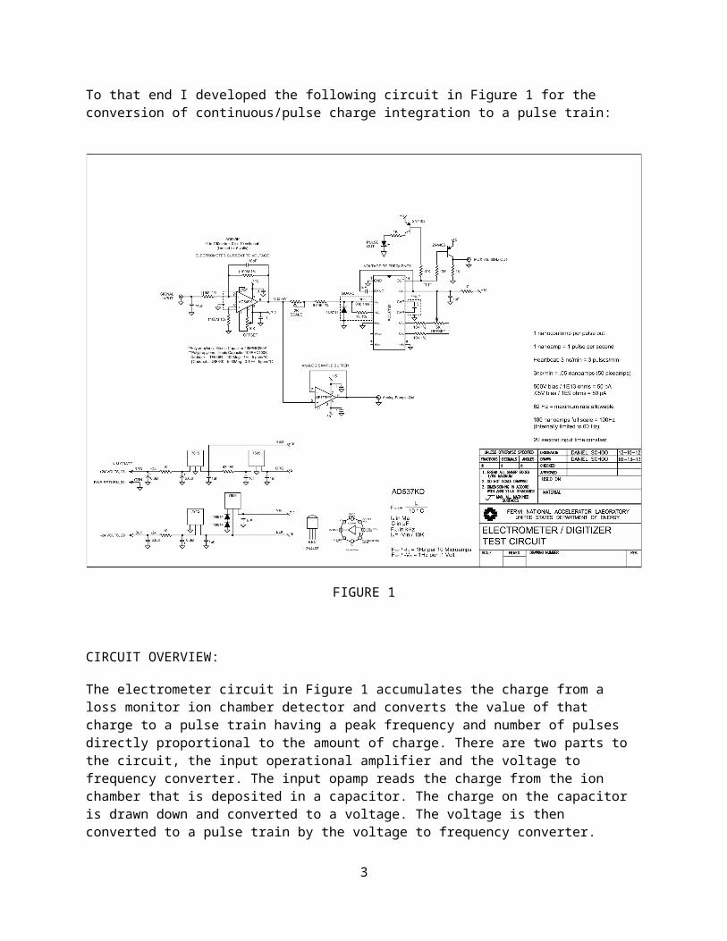
FIGURE 1
CIRCUIT OVERVIEW:
The electrometer circuit in Figure 1 accumulates the charge from a loss monitor ion chamber detector and converts the value of that charge to a pulse train having a peak frequency and number of pulses directly proportional to the amount of charge. There are two parts to the circuit, the input operational amplifier and the voltage to frequency converter. The input opamp reads the charge from the ion chamber that is deposited in a capacitor. The charge on the capacitor is drawn down and converted to a voltage. The voltage is then converted to a pulse train by the voltage to frequency converter.
CIRCUIT FUNCTION:
DetectorThe detector consists of a length of 7/8 inch diameter Andrew Heliax® cable. The cable is of the “air filled” type with a spiral polyethylene spacer between the outer copper sleeve and inner conductor. The two ends are terminated with caps that have two electrical connectors, a BNC connected to the inner conductor for signal and an SHV high voltage connector connected to the outer sleeve for bias. A gas connection port is also supplied to allow filling the empty space inside the cable with argon or an argon /
3
carbon dioxide mix. In normal operation a constant positive bias of 500 volts is applied to the outer sleeve. This provides the means of collecting the positive ionic current on the center conductor. As such the detector forms an essentially infinite impedance current source that delivers a charge directly proportional to the amount of ionizing radiation that passes through the space inside the cable.
Current to Voltage AmplifierThe input amplifier is an Analog Devices AD549 monolithic integrated circuit Ultra Low Input Bias Current Operational Amplifier. The AD549 has an input bias of typically 75 femtoamps to maintain negligible contribution of the bias to the measured signal and is packaged in a grounded metal can to minimize electromagnetic interference.2
The capacitor on the signal input absorbs and stores the charge developed in the detector. The resulting voltage on the capacitor (V) is equal to the charge in coulombs (Q) divided by the value of the capacitance in farads (C).
V=QC
For the normal range of operational losses this is expected to be in the range of zero to tens of millivolts. The operational amplifier draws the deposited charge from the capacitor through the input resistor into a virtual ground point at the inverting input. The virtual ground is normally kept at zero volts by a current provided through the feedback resistor equal to the input current but opposite in polarity such that the sum of currents at the virtual ground is zero.
The input capacitor performs several functions. First, it absorbs and holds the charge from the ion chamber allowing the input opamp to draw it down over time and report all of the charge at a rate that is within the limit of the MUX to accept. Second, along with the input resistor, it provides the required 20 second time constant. Third, it provides a low impedance AC path to ground for noise and hum. The input capacitor must be a type with minimal dielectric absorption such as polypropylene or Teflon™ in order to prevent retention of part of the charge.
The value of the input capacitor must be chosen taking into account several factors. A smaller value capacitor reaches a higher voltage with a given value of charge, especially for high beam losses. The disadvantage is higher voltages encourage higher leakage currents inside and around the capacitor. For very large charges the voltage could become excessively large possibly overscaling or damaging the input opamp. A small value of capacitance also requires a high value of input resistor to provide the 20 second time constant. A larger value of capacitor lowers the voltage developed with a given charge promoting lower leakage and a better margin of safety for gross overscales. It also allows a lower value of input resistor. Very large capacitance keeps the input voltages very low inviting noise problems. Large value capacitors are also physically large and are difficult to place.
As charge is deposited to the input capacitor the opamp draws it out and converts the value of charge to a voltage. The output voltage of the opamp is directly proportional to the remaining charge on the capacitor and thus follows a decaying exponential conforming to the 20 second time constant.
Since a loss monitor ion chamber is essentially an infinite impedance current source, the value of the input resistor is not a factor in the ultimate charge to voltage conversion gain from the detector. The only effect that the value of the input resistance has is to govern the rate at which the charge is removed from the input capacitor and reported. This is exactly what is desired for the 20 second time
4
constant. The value of the resistor is chosen in conjunction with the value of the input capacitor to provide the 20 second time constant.
The input current-to-voltage conversion gain is determined by the 100 Meg feedback resistor. The voltage drop developed across this resistor is .1 volts per nanoamp. This translates to a conversion factor of 10 volts out for 100 nanoamps of current into the virtual ground node at the inverting input. The 10 picofarad capacitor shunting the feedback resistor rolls off the high frequency gain to suppress noise pickup and promote stability. There is a matching 100 Meg resistor from the non-inverting input to ground. This is to reference the non-inverting input to ground potential and balance the bias current voltage drops to minimize offset.
These two resistors are very sensitive to vibration due to charge induced by changes in capacitance to ground and internal stresses. For my breadboard test circuit I used Caddock TF series ultra-precision film resistors that are manufactured on a flat ceramic substrate. They are excellent resistors but because of their large flat physical configuration they are highly prone to capacitance to ground changes with vibration. Covering them with copper tape and grounding the tape helped to minimize but not eliminate this problem. The Caddock CHR surface mount resistor is specifically designed for electrometer service with ion chambers and other charge amplifier applications. I used these in the NIM module test and they were considerably less sensitive to vibration. These effects should be taken into account in the final assembly by careful shielding and vibration damping of the sensitive input circuit components.
One very important function of the electrometer is to limit the rate at which the loss is reported to the MUX. The MUX system is limited to an input pulse rate of about 70Hz maximum. In the Chipmunk detectors the 20 second time constant provides this function.1
I limited the reporting rate of this circuit to 60 Hz. In order to do this, the negative supply voltage for the input opamp is such that the amplifier’s output voltage saturates at about -6 volts representing a 60 pulse per second rate. This limits the current that the opamp can provide into the virtual ground point through the feedback resistor slowing the rate at which the charge is depleted from the capacitor. While the reporting rate is limited it does not cause any loss of data. Any charge that would cause a rate above the maximum value remains in the input capacitor and is reported out at the limited rate. As the charge is depleted it eventually goes below the 60 Hz limit and the pulse frequency resumes the normal rate following the value of the remaining charge until all of the charge has been converted and reported.
This limit must be imposed inside the opamp feedback loop on the rate at which the charge is drawn from the capacitor. If the limit were placed at any other part of the circuit, for example at the voltage to frequency conversion, the charge would continue to be drawn from the capacitor at a rate higher than is being reported causing the excess charge to be unreported. A voltage limiting circuit could be imposed on the output of the opamp inside the feedback loop but this would add complication and additional parts count to the design. By limiting the negative supply voltage the opamp is necessarily limited to the maximum rate with no additional components and no ill effects to the performance.
Voltage to Frequency ConverterThe voltage to frequency converter follows the input amplifier. I selected an Analog Devices AD537 precision monolithic Integrated Circuit Voltage-to-Frequency Converter in the interest of expediency because of prior experience with this device and samples in stock. It has a specified dynamic range of 80dbv or 1 millivolt useable minimum to 10 volts maximum full scale. It is normally used with a 0 to +10
5
volt input but can also be configured for a 0 to -1 milliamp input. In this mode the dynamic range is 100 nanoamps useable minimum to 1 milliamp maximum.3 in this application the charge from the loss monitor is a positive current and the input amplifier is an inverting type resulting in a 0 to -10 volt output. Rather than add the additional complication and error of another operational amplifier to invert this signal I used the 0 to -1 milliamp mode with a series scaling resistor to convert the 0 to -10 volts from the amplifier to a 0 to -1 milliamp current.
The internal circuit of the AD537 consists of two parts, an operational amplifier and a current to frequency converter. The operational amplifier is used as a voltage to current converter to convert the input voltage to a current for the current to frequency converter.4 Together they form a Current Steering Voltage to Frequency Converter. In the Current Steering Current to Frequency Converter the input current charges a capacitor causing the voltage across the capacitor to rise at a rate depending on the charge current. When the voltage across the capacitor reaches a fixed threshold the capacitor polarity is reversed and the input current discharges it. The capacitor voltage decreases and when a lower threshold voltage is reached the capacitor polarity is switched back and the process repeats.5 Larger currents cause the capacitor to charge and discharge more quickly raising the frequency of the switching rate. The switching thresholds are set by a stable reference, and the output is a frequency proportional to the input voltage or current depending on the configuration.
One problem with this converter is described in the datasheet. “Below 100 nA improper operation of the oscillator may result, causing a false indication of input amplitude. In many cases this might be due to short-lived noise spikes which become added to the input. For example, when scaled to accept a FS input of 1 V, the –80 dB level is only 100 μV, so when the mean input is only 60 dB below FS (1 mV), noise spikes of 0.9 mV are sufficient to cause momentary malfunction.”3 This is quite evident when the signal levels approach zero and the pulse output intermittently flutters. The heartbeat signal is more than adequate to suppress this problem or the offset of the V/F internal amplifier can be adjusted such that it applies a sufficient current into the converter to keep the signal level from dropping too low.
The frequency range of the V/F converter is set by a single external capacitor and resistor. The capacitor value is calculated for the frequency range desired using the following equation:
f= I10.5∗C
Where f is in kHz, I is in mA and C is in μF. In this case for a 100Hz full scale frequency at 1 milliamp of input current the value of C is close to 1uf. The integration capacitor must be a type with minimal dielectric absorption such as polypropylene or Teflon™.
The resistor value is calculated to provide a 0 to -1 milliamp current for 0 to -10 volts, nominally 10K ohms. In practice a 9.09K resistor in series with a 2K trimming potentiometer is used to provide a means of trimming the full scale calibration to the desired value. This combined with the conversion factor of the input opamp of .1 volt out per nanoamp in, provides the required overall conversion factor of one Hz per nanoamp or, in terms of charge, one pulse per nanocoulomb of collected charge.
The output pulses are symmetrical square waves. The pulse output uses an open collector NPN transistor driver capable of sinking up to 20 milliamps. The output from the V/F is buffered externally by a common emitter PNP transistor switch with a 1K ohm pulldown resistor to ground in the collector
6

circuit and the emitter connected to +5 volts. This is the same circuit used in the Chipmunk pulse output to the MUX and was included to facilitate complete compatibility.
In this configuration the transistor can be destroyed from excessive current by attempting to drive a shorted load. The transistor is protected from short circuit loads by a current limiting resistor placed on the input side of the +5 volt regulator. If excessive current is drawn from the pulse output the resistor will drop sufficient voltage on the input side of the +5 volt regulator to cause the regulator to drop out of regulation and safely limit the current to a level that will not damage the transistor. During normal operation the regulator has sufficient voltage differential to remain in regulation and provide the proper voltage level.
A second identical buffer transistor drives a front panel mounted light emitting diode as a visual indication of the output pulses to help in testing and verification of operational integrity.
There is another type of V/F converter chip available from Analog Devices, the AD650, which is based on the Charge Balance conversion method. It does not exhibit the near zero instability problem and has significantly better specifications.6 The AD650 is about $20 each as compared to the AD537 at about $80. I have obtained samples of this chip and have done preliminary breadboard tests on it. It shows an order of magnitude improvement in sensitivity and at least two orders of magnitude better linearity than the AD537, even in a breadboard environment. In order to get something in the field to test, the completed AD537 version will be tested first followed by the AD650 version when it becomes available. A full report similar to this one on the AD537 will be forthcoming including a comparable set of test results.
Analog Sample BufferThe sample buffer is a unity gain non-inverting amplifier included for testing purposes. It is often beneficial to be able to sample the analog signal to evaluate noise problems or for troubleshooting and calibration without disturbing or loading the internal signal path. It may or may not be included in the final production version for diagnostic signal sampling and/or calibration purposes.
This combination of integrated circuits, in a negative signal input configuration, has been in common usage for many years as the Fixed Target SEM Current Digitizer module and has proven to be very reliable and stable.
7
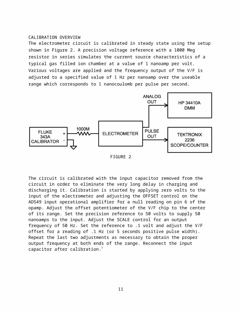
CALIBRATION OVERVIEWThe electrometer circuit is calibrated in steady state using the setup shown in Figure 2. A precision voltage reference with a 1000 Meg resistor in series simulates the current source characteristics of a typical gas filled ion chamber at a value of 1 nanoamp per volt. Various voltages are applied and the frequency output of the V/F is adjusted to a specified value of 1 Hz per nanoamp over the useable range which corresponds to 1 nanocoulomb per pulse per second.
FIGURE 2
The circuit is calibrated with the input capacitor removed from the circuit in order to eliminate the very long delay in charging and discharging it. Calibration is started by applying zero volts to the input of the electrometer and adjusting the OFFSET control on the AD549 input operational amplifier for a null reading on pin 6 of the opamp. Adjust the offset potentiometer of the V/F chip to the center of its range. Set the precision reference to 50 volts to supply 50 nanoamps to the input. Adjust the SCALE control for an output frequency of 50 Hz. Set the reference to .1 volt and adjust the V/F offset for a reading of .1 Hz (or 5 seconds positive pulse width). Repeat the last two adjustments as necessary to obtain the proper output frequency at both ends of the range. Reconnect the input capacitor after calibration.7
8
TESTING and VERIFICATION of ACCURACY
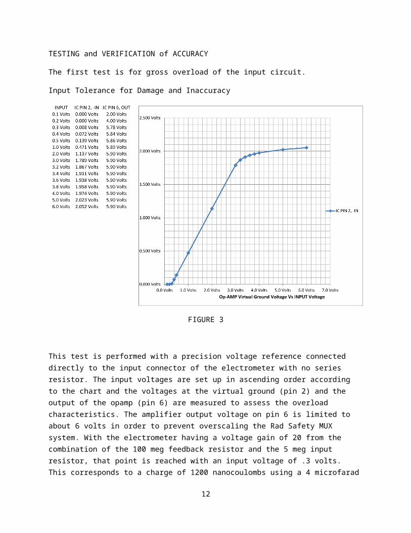
The first test is for gross overload of the input circuit.
Input Tolerance for Damage and Inaccuracy
FIGURE 3
This test is performed with a precision voltage reference connected directly to the input connector of the electrometer with no series resistor. The input voltages are set up in ascending order according to the chart and the voltages at the virtual ground (pin 2) and the output of the opamp (pin 6) are measured to assess the overload characteristics. The amplifier output voltage on pin 6 is limited to about 6 volts in order to prevent overscaling the Rad Safety MUX system. With the electrometer having a voltage gain of 20 from the combination of the 100 meg feedback resistor and the 5 meg input resistor, that point is reached with an input voltage of .3 volts. This corresponds to a charge of 1200 nanocoulombs using a 4 microfarad input capacitor. Above that voltage the amplifier output is in saturation and no longer able to maintain the virtual ground node on pin 2 at ground potential. It does however maintain a linear relationship between the input voltage and the virtual ground node until the input voltage reaches about 3.0 volts corresponding to about 12,000 nanocoulombs of charge. At this point the curve breaks downward indicating that the charge current is beginning to be diverted
9

elsewhere other than through the feedback resistor. This implies that the input voltage should not be allowed to exceed 3.0 volts to maintain proper function of the electrometer.
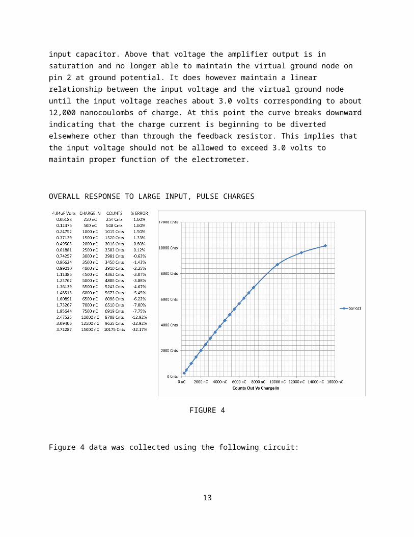
OVERALL RESPONSE TO LARGE INPUT, PULSE CHARGES
FIGURE 4
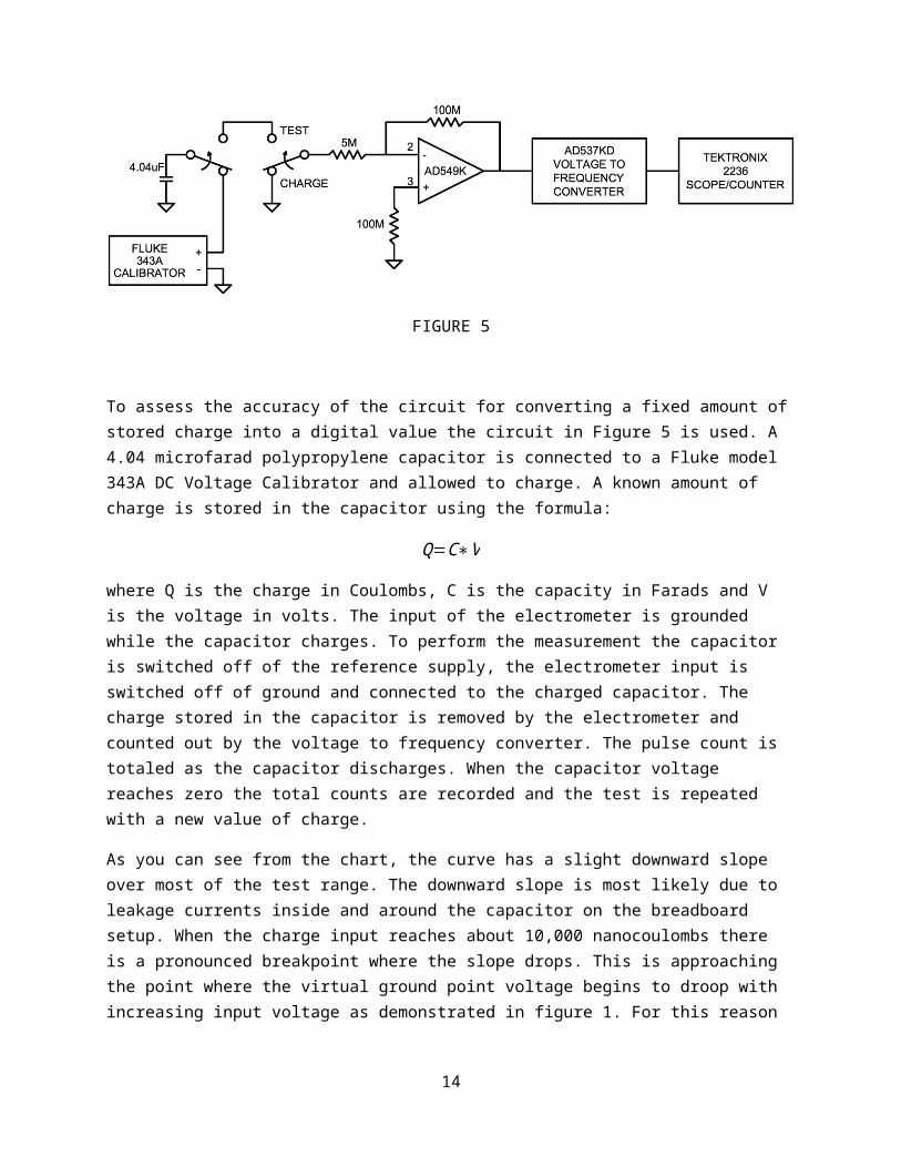
Figure 4 data was collected using the following circuit:
FIGURE 5
10
To assess the accuracy of the circuit for converting a fixed amount of stored charge into a digital value the circuit in Figure 5 is used. A 4.04 microfarad polypropylene capacitor is connected to a Fluke model 343A DC Voltage Calibrator and allowed to charge. A known amount of charge is stored in the capacitor using the formula:
Q=C∗V
where Q is the charge in Coulombs, C is the capacity in Farads and V is the voltage in volts. The input of the electrometer is grounded while the capacitor charges. To perform the measurement the capacitor is switched off of the reference supply, the electrometer input is switched off of ground and connected to the charged capacitor. The charge stored in the capacitor is removed by the electrometer and counted out by the voltage to frequency converter. The pulse count is totaled as the capacitor discharges. When the capacitor voltage reaches zero the total counts are recorded and the test is repeated with a new value of charge.
As you can see from the chart, the curve has a slight downward slope over most of the test range. The downward slope is most likely due to leakage currents inside and around the capacitor on the breadboard setup. When the charge input reaches about 10,000 nanocoulombs there is a pronounced breakpoint where the slope drops. This is approaching the point where the virtual ground point voltage begins to droop with increasing input voltage as demonstrated in figure 1. For this reason the circuit cannot be expected to report correct values of charge above this value unless the input capacitor value is changed.
OVERALL RESPONSE TO NORMAL RANGE INPUT, PULSE CHARGES
FIGURE 6
11
The chart in Figure 6 shows the pulse charge readings using the Figure 5 test circuit from 100 nanocoulombs down to the lowest pulse measurement level of 1 nanocoulomb. The response to input charge is quite accurate over the typical expected operating range of 1 to 50 nanocoulombs.
OVERALL RESPONSE TO NORMAL RANGE INPUT, CONTINUOUS CHARGES
VERY LOW RANGE RANGEBecause the circuit is designed to produce only one pulse per nanocoulomb, the pulse charge test is only applicable down to the 1 nanocoulomb level. To measure the response of the circuit to charges of less than 1 nanocoulomb, it is necessary to apply a continuous current of 1 nanoamp or less over a period of time in order to build up enough charge to get a pulse response. To assess the accuracy of the circuit for converting a sub nanocoulomb charge into a continuous pulse train the circuit in Figure 7 is used.
FIGURE 7
FIGURE 8
12
In Figure 8 we see the performance in the very low range from 1 nanoamp and lower. Because of the very low repetition rate the counter is set up in the Pulse Width mode to read the number of seconds per count rather than the number of counts per second. Even at this low level the percentage of error from the ideal is small.
ULTRA LOW RANGE
FIGURE 9
Finally we get to the Ultra Low Range where we are scraping the bottom of the charge barrel. Like the Very Low Range measurement we must measure seconds per pulse rather than pulses per second. Because of the very long delay times involved, my Tek scope / counter was unable to wait that long between pulses to display the width time. In order to make the ultra long time measurements I used the test setup shown in Figure 9.
The pulse output of the electrometer is used to gate the output of a Hewlett-Packard model 3325B function generator set up to provide 2000 Hz sine waves. The 2000 Hz output is gated on and off by the positive pulse output from the electrometer. The number of 2000 Hz cycles in the resulting gated burst is directly proportional to the amount of time that the pulse output is positive in milliseconds. Because the gate is positive for only half of the total repetition rate, a 2000 Hz signal is used to multiply the positive gate time by two. To measure the repetition rate in milliseconds the total number of 2000 Hz cycles for one positive excursion of the pulse output is counted on the Tektronix model 2236 scope / timer and the number is recorded.
13
The chart shows a mild droop in the readings below the .1 nanoamp level. By the time the .01 level is reached the error is more than 10%. At this point the V/F converter is reading voltages below 1 millivolt and subject to noise, thermoelectric and drift effects in the entire chain. At the .05 nanoamp level of the heartbeat, the error is not excessive and the circuit is able to report that amount of charge reliably. Further tests and study will be necessary in the field to assess the actual performance in a real world detector situation.
References:
1. “Preliminary Test Results, Dynamic Range Requirements, and TLM Electrometer Requirements for Total Loss Monitor (TLM) Systems at Fermilab” A. Leveling, J. Anderson, P. Czarapata, October 5, 2012
2. Datasheet “Analog Devices Ultralow Input Bias Current Operational Amplifier AD549” Revision H, 2008
3. Datasheet “Analog Devices Integrated Circuit Voltage to Frequency Converter AD537”, Revision C, undated
4. Analog Devices AN-277 Application Note, “Applications of the AD537 IC Voltage-to-Frequency Converter” Barrie Gilbert and Doug grant, undated
5. Analog Devices MT-028 Tutorial, “Voltage-to-Frequency Converters” Walt Kester, James Bryant, 2009http://www.analog.com/static/imported-files/tutorials/MT-028.pdf
6. Datasheet “Analog Devices Voltage-to-Frequency and Frequency-to-Voltage Converter AD650” Revision D, 2006
7. Calibration Procedure for the LLM Electrometer Charge to Pulse Train Converter Circuit, Daniel Schoo, March 2013
14


![Real Insulators (Dielectrics) If I bring a charged rod to a leaf electrometer: A] nothing will happen B] nothing will happen until I touch the electrometer](https://img.pdfslide.us/doc/110x75/56649d375503460f94a10048/real-insulators-dielectrics-if-i-bring-a-charged-rod-to-a-leaf-electrometer.jpg)