Embed Size (px)
Citation preview
1. General description
The UJA1167A is a mini high-speed CAN System Basis Chip (SBC) containing an ISO 11898-2:2016 and SAE J2284-1 to SAE J2284-5 compliant HS-CAN transceiver and an integrated 5 V/100 mA supply for a microcontroller. It also features a watchdog and a Serial Peripheral Interface (SPI). The UJA1167A can be operated in very-low-current Standby and Sleep modes with bus and local wake-up capability and supports ISO 11898-2:2016 compliant autonomous CAN biasing. The microcontroller supply is switched off in Sleep mode.
The UJA1167ATK variant contains a battery-related high-voltage output (INH) for controlling an external voltage regulator, while the UJA1167ATK/X is equipped with a 5 V sensor supply (VEXT).
This implementation enables reliable communication in the CAN FD fast phase at data rates up to 5 Mbit/s.
A number of configuration settings are stored in non-volatile memory, allowing the SBC to be adapted for use in a specific application. This makes it possible to configure the power-on behavior of the UJA1167A to meet the requirements of different applications.
2. Features and benefits
2.1 General
ISO 11898-2:2016 and SAE J2284-1 to SAE J2284-5 compliant high-speed CAN transceiver
Hardware and software compatible with the UJA116x product family and with improved EMC performance
Loop delay symmetry timing enables reliable communication at data rates up to 5 Mbit/s in the CAN FD fast phase
Autonomous bus biasing according to ISO 11898-6
Fully integrated 5 V/100 mA low-drop voltage regulator for 5 V microcontroller supply (V1)
Bus connections are truly floating when power to pin BAT is off
2.2 Designed for automotive applications
8 kV ElectroStatic Discharge (ESD) protection, according to the Human Body Model (HBM) on the CAN bus pins
6 kV ESD protection, according to IEC TS 62228 on the CAN bus pins, the sensor supply output VEXT and on pins BAT and WAKE
UJA1167AMini high-speed CAN system basis chip with Standby/Sleep modes & watchdogRev. 1 — 23 August 2019 Product data sheet

NXP Semiconductors UJA1167AMini high-speed CAN system basis chip with Standby/Sleep modes &
watchdog
CAN bus pins short-circuit proof to 58 V
Battery and CAN bus pins protected against automotive transients according to ISO 7637-3
Very low quiescent current in Standby and Sleep modes with full wake-up capability
Leadless HVSON14 package (3.0 mm 4.5 mm) with improved Automated Optical Inspection (AOI) capability and low thermal resistance
Dark green product (halogen free and Restriction of Hazardous Substances (RoHS) compliant)
2.3 Low-drop voltage regulator for 5 V microcontroller supply (V1)
5 V nominal output; 2 % accuracy
100 mA output current capability
Current limiting above 150 mA
On-resistance of 5 (max)
Support for microcontroller RAM retention down to a battery voltage of 2 V
Undervoltage reset with selectable detection thresholds: 60 %, 70 %, 80 % or 90 % of output voltage
Excellent transient response with a 4.7 F ceramic output capacitor
Short-circuit to GND/overload protection on pin V1
Turned off in Sleep mode
2.4 Power Management
Standby mode featuring very low supply current; voltage V1 remains active to maintain the supply to the microcontroller
Sleep mode featuring very low supply current with voltage V1 switched off
Remote wake-up capability via standard CAN wake-up pattern
Local wake-up via the WAKE pin
Wake-up source recognition
Local and/or remote wake-up can be disabled to reduce current consumption
High-voltage output (INH) for controlling an external voltage (UJA1167ATK)
2.5 System control and diagnostic features
Mode control via the Serial Peripheral Interface (SPI)
Overtemperature warning and shutdown
Watchdog with independent clock source
Watchdog can be operated in Window, Timeout and Autonomous modes
Optional cyclic wake-up in watchdog Timeout mode
Watchdog automatically re-enabled when wake-up event captured
Watchdog period selectable between 8 ms and 4 s
Supports remote flash programming via the CAN bus
16-, 24- and 32-bit SPI for configuration, control and diagnosis
Bidirectional reset pin with variable power-on reset length to support a variety of
microcontrollers
Configuration of selected functions via non-volatile memory
UJA1167A All information provided in this document is subject to legal disclaimers. © NXP Semiconductors N.V. 2019. All rights reserved.
Product data sheet Rev. 1 — 23 August 2019 2 of 66
NXP Semiconductors UJA1167AMini high-speed CAN system basis chip with Standby/Sleep modes &
watchdog
2.6 Sensor supply voltage (pin VEXT of UJA1167ATK/X)
5 V nominal output; 2 % accuracy
30 mA output current capability
Current limiting above 30 mA
Excellent transient response with a 4.7 F ceramic output load capacitor
Protected against short-circuits to GND and to the battery
High ESD robustness of 6 kV according to IEC TS 62228
Can handle negative voltages as low as 18 V
UJA1167A All information provided in this document is subject to legal disclaimers. © NXP Semiconductors N.V. 2019. All rights reserved.
Product data sheet Rev. 1 — 23 August 2019 3 of 66
NXP Semiconductors UJA1167AMini high-speed CAN system basis chip with Standby/Sleep modes &
watchdog
3. Product family overview
4. Ordering information
[1] UJA1167ATK contains a high-voltage output for controlling an external voltage regulatror; UJA1167ATK/X includes a 5 V/30 mA sensor supply.
Table 1. Feature overview of UJA1167A SBC family
Modes Supplies Host Interface Additional Features
Device No
rmal
& S
tan
db
y m
od
es
Sle
ep m
od
e
Res
et
mo
de
V1:
5V
, C
an
d C
AN
VE
XT:
5V
, ext
ern
al lo
ads
INH
: h
igh
-vo
ltag
e o
utp
ut
SP
I: f
or
con
tro
l & d
iag
no
stic
s
RS
TN
: re
set
pin
Wat
chd
og
Lo
cal W
AK
E p
in
No
n-v
ola
tile
mem
ory
UJA1167ATK ● ● ● ● ● ● ● ● ● ●
UJA1167ATK/X ● ● ● ● ● ● ● ● ● ●
Table 2. Ordering information
Type number[1] Package
Name Description Version
UJA1167ATK HVSON14 plastic thermal enhanced very thin small outline package; no leads; 14 terminals; body 3 4.5 0.85 mm
SOT1086-2
UJA1167ATK/X
UJA1167A All information provided in this document is subject to legal disclaimers. © NXP Semiconductors N.V. 2019. All rights reserved.
Product data sheet Rev. 1 — 23 August 2019 4 of 66
NXP Semiconductors UJA1167AMini high-speed CAN system basis chip with Standby/Sleep modes &
watchdog
5. Block diagram
(1) UJA1167ATK only.
(2) UJA1167ATK/X only.
Fig 1. Block diagram of UJA1167A
UJA1167A
BAT HIGH VOLTAGE OUTPUT (1) INH(1)/VEXT(2)
5 V SENSOR SUPPLY(2)
5 V MICROCONTROLLER SUPPLY (V1)RSTN
V1
WATCHDOG
HS-CAN CANH
CANLTXD
RXD
WAKE WAKE-UP
SDI
SCK
SCSN
SDOSPI
aaa-022892
7
5
3
13
12
10
4
1
9
8
11
6
14
GND
2
UJA1167A All information provided in this document is subject to legal disclaimers. © NXP Semiconductors N.V. 2019. All rights reserved.
Product data sheet Rev. 1 — 23 August 2019 5 of 66

NXP Semiconductors UJA1167AMini high-speed CAN system basis chip with Standby/Sleep modes &
watchdog
6. Pinning information
6.1 Pinning
6.2 Pin description
[1] The exposed die pad at the bottom of the package allows for better heat dissipation and grounding from the SBC via the printed circuit board. For enhanced thermal and electrical performance, it is recommended to solder the exposed die pad to GND.
(1) INH in the UJA1167ATK; VEXT in the UJA1167ATK/X
Fig 2. Pin configuration diagram
terminal 1index area
aaa-022893
UJA1167A
TXD 1
GND 2
3
RXD 4
5
SDO 6
INH/VEXT(1)
SCSN
CANH
CANL
SDI
BAT
WAKE
SCK7
14
13
12
11
10
9
8
Transparent top view
V1
RSTN
Table 3. Pin description
Symbol Pin Description
TXD 1 transmit data input
GND 2[1] ground
V1 3 5 V microcontroller supply voltage
RXD 4 receive data output; reads out data from the bus lines
RSTN 5 reset input/output
SDO 6 SPI data output
INH 7 high-voltage output for switching external regulators (UJA1167ATK)
VEXT 7 sensor supply voltage (UJA1167ATK/X)
SCK 8 SPI clock input
WAKE 9 local wake-up input
BAT 10 battery supply voltage
SDI 11 SPI data input
CANL 12 LOW-level CAN bus line
CANH 13 HIGH-level CAN bus line
SCSN 14 SPI chip select input
UJA1167A All information provided in this document is subject to legal disclaimers. © NXP Semiconductors N.V. 2019. All rights reserved.
Product data sheet Rev. 1 — 23 August 2019 6 of 66

NXP Semiconductors UJA1167AMini high-speed CAN system basis chip with Standby/Sleep modes &
watchdog
7. Functional description
7.1 System controller
The system controller manages register configuration and controls the internal functions of the UJA1167A. Detailed device status information is collected and made available to the microcontroller.
7.1.1 Operating modes
The system controller contains a state machine that supports seven operating modes: Normal, Standby, Sleep, Reset, Forced Normal, Overtemp and Off. The state transitions are illustrated in Figure 3.
7.1.1.1 Normal mode
Normal mode is the active operating mode. In this mode, all the hardware on the device is available and can be activated (see Table 4). Voltage regulator V1 is enabled to supply the microcontroller.
The CAN interface can be configured to be active and thus to support normal CAN communication. Depending on the SPI register settings, the watchdog may be running in Window or Timeout mode and the INH/VEXT output may be active.
Normal mode can be selected from Standby mode via an SPI command (MC = 111).
7.1.1.2 Standby mode
Standby mode is the first-level power-saving mode of the UJA1167A, offering reduced current consumption. The transceiver is unable to transmit or receive data in Standby mode. The SPI remains enabled and V1 is still active; the watchdog is active (in Timeout mode) if enabled. The behavior of INH/VEXT is determined by the SPI setting.
If remote CAN wake-up is enabled (CWE = 1; see Table 27), the receiver monitors bus activity for a wake-up request. The bus pins are biased to GND (via Ri(cm)) when the bus is inactive for t > tto(silence) and at approximately 2.5 V when there is activity on the bus (autonomous biasing).
Pin RXD is forced LOW when any enabled wake-up event is detected. This can be either a regular wake-up (via the CAN bus or pin WAKE) or a diagnostic wake-up such as an overtemperature event (see Section 7.10).
The UJA1167A switches to Standby mode via Reset mode:
• from Off mode if the battery voltage rises above the power-on detection threshold (Vth(det)pon)
• from Overtemp mode if the chip temperature falls below the overtemperature protection release threshold, Tth(rel)otp
• from Sleep mode on the occurrence of a regular or diagnostic wake-up event
Standby mode can also be selected from Normal mode via an SPI command (MC = 100).
UJA1167A All information provided in this document is subject to legal disclaimers. © NXP Semiconductors N.V. 2019. All rights reserved.
Product data sheet Rev. 1 — 23 August 2019 7 of 66

NXP Semiconductors UJA1167AMini high-speed CAN system basis chip with Standby/Sleep modes &
watchdog
7.1.1.3 Sleep mode
Sleep mode is the second-level power-saving mode of the UJA1167A. The difference between Sleep and Standby modes is that V1 is off in Sleep mode and temperature protection is inactive.
Fig 3. UJA1167A system controller state diagram
NORMAL
STANDBY
MC = Sleep &no wake-up pending &
wake-up enabled &SLPC = 0
MC = Sleep &no wake-up pending &
wake-up enabled &SLPC = 0
MC = Normal
MC = Standby
aaa-016003
SLEEP
no overtemperature
OVERTEMP
RSTN = HIGH &FNMC = 0
overtemperature event
from any mode except Off & Sleep
RESET
power-on
OFF
from any mode
VBAT undervoltage
V1 undervoltage
any reset event
FORCEDNORMAL
any reset event
from Normal or Standby
MC = Sleep &(wake-up pending OR wake-up disabled OR
SLPC = 1)
wake-up event
MTP programming completed orMTP factory presets restored
RSTN = HIGH & FNMC = 1
UJA1167A All information provided in this document is subject to legal disclaimers. © NXP Semiconductors N.V. 2019. All rights reserved.
Product data sheet Rev. 1 — 23 August 2019 8 of 66
NXP Semiconductors UJA1167AMini high-speed CAN system basis chip with Standby/Sleep modes &
watchdog
Any enabled regular wake-up via CAN or WAKE or any diagnostic wake-up event will cause the UJA1167A to wake up from Sleep mode. The behavior of INH/VEXT is determined by the SPI settings. The SPI is disabled. Autonomous bus biasing is active. See Table 7 for a description of watchdog behavior in Sleep mode.
Sleep mode can be selected from Normal or Standby mode via an SPI command (MC = 001). The UJA1167A will switch to Sleep mode on receipt of this command, provided there are no pending wake-up events and at least one regular wake-up source is enabled. Any attempt to enter Sleep mode while one of these conditions has not been met will cause the UJA1167A to switch to Reset mode and set the reset source status bits (RSS) to 10100 (‘illegal Sleep mode command received’; see Table 6).
Since V1 is off in Sleep mode, the only way the SBC can exit Sleep mode is via a wake-up event (see Section 7.10).
Sleep mode can be permanently disabled in applications where, for safety reasons, the supply voltage to the host controller must never be cut off. Sleep mode is permanently disabled by setting the Sleep control bit (SLPC) in the SBC configuration register (see Table 9) to 1. This register is located in the non-volatile memory area of the device. When SLPC = 1, a Sleep mode SPI command (MC = 001) triggers an SPI failure event instead of a transition to Sleep mode.
7.1.1.4 Reset mode
Reset mode is the reset execution state of the SBC. This mode ensures that pin RSTN is pulled down for a defined time to allow the microcontroller to start up in a controlled manner.
The transceiver is unable to transmit or receive data in Reset mode. The behavior of INH/VEXT is determined by the settings of bits VEXTC and VEXTSUC (see Section 7.6). The SPI is inactive; the watchdog is disabled; V1 and overtemperature detection are active.
The UJA1167A switches to Reset mode from any mode in response to a reset event (see Table 6 for a list of reset sources).
The UJA1167A exits Reset mode:
• and switches to Standby mode if pin RSTN is released HIGH
• and switches to Forced Normal mode if bit FNMC = 1
• if the SBC is forced into Off or Overtemp mode
If a V1 undervoltage event forced the transition to Reset mode, the UJA1167A will remain in Reset mode until the voltage on pin V1 has recovered.
7.1.1.5 Off mode
The UJA1167A switches to Off mode when the battery is first connected or from any mode when VBAT < Vth(det)poff. Only power-on detection is enabled; all other modules are inactive. The UJA1167A starts to boot up when the battery voltage rises above the power-on detection threshold Vth(det)pon (triggering an initialization process) and switches to Reset mode after tstartup. In Off mode, the CAN pins disengage from the bus (zero load; high-ohmic).
UJA1167A All information provided in this document is subject to legal disclaimers. © NXP Semiconductors N.V. 2019. All rights reserved.
Product data sheet Rev. 1 — 23 August 2019 9 of 66
NXP Semiconductors UJA1167AMini high-speed CAN system basis chip with Standby/Sleep modes &
watchdog
7.1.1.6 Overtemp mode
Overtemp mode is provided to prevent the UJA1167A being damaged by excessive temperatures. The UJA1167A switches immediately to Overtemp mode from any mode (other than Off mode or Sleep mode) when the global chip temperature rises above the overtemperature protection activation threshold, Tth(act)otp.
To help prevent the loss of data due to overheating, the UJA1167A issues a warning when the IC temperature rises above the overtemperature warning threshold (Tth(warn)otp). When this happens, status bit OTWS is set and an overtemperature warning event is captured (OTW = 1), if enabled (OTWE = 1).
In Overtemp mode, the CAN transmitter and receiver are disabled and the CAN pins are in a high-ohmic state. No wake-up event will be detected, but a pending wake-up will still be signalled by a LOW level on pin RXD, which will persist after the overtemperature event has been cleared. V1 is off and pin RSTN is driven LOW.
VEXT is off in the UJA1167ATK/X. In the UJA1167ATK, INH remains unchanged when the SBC enters Overtemp mode.
The UJA1167A exits Overtemp mode:
• and switches to Reset mode if the chip temperature falls below the overtemperature protection release threshold, Tth(rel)otp
• if the device is forced to switch to Off mode (VBAT < Vth(det)poff)
7.1.1.7 Forced Normal mode
Forced Normal mode simplifies SBC testing and is useful for initial prototyping and failure detection, as well as first flashing of the microcontroller. The watchdog is disabled in Forced Normal mode. The low-drop voltage regulator (V1) is active, VEXT/INH is enabled and the CAN transceiver is active.
Bit FNMC is factory preset to 1, so the UJA1167A initially boots up in Forced Normal mode (see Table 9). This allows a newly installed device to be run in Normal mode without a watchdog. So the microcontroller can be flashed via the CAN bus in the knowledge that a watchdog timer overflow will not trigger a system reset.
The register containing bit FNMC (address 74h) is stored in non-volatile memory (see Section 7.11). So once bit FNMC is programmed to 0, the SBC will no longer boot up in Forced Normal mode, allowing the watchdog to be enabled.
Even in Forced Normal mode, a reset event (e.g. an external reset or a V1 undervoltage) will trigger a transition to Reset mode with normal Reset mode behavior (except that the transmitter remains active if there is no V1 undervoltage). However, the UJA1167A will return to Forced Normal mode instead of switching to Standby mode when it exits Reset mode.
In Forced Normal mode, only the Main status register, the Watchdog status register, the Identification register and registers stored in non-volatile memory can be read. The non-volatile memory area is fully accessible for writing as long as the UJA1167A is in the factory preset state (for details see Section 7.11).
The UJA1167A switches from Reset mode to Forced Normal mode if bit FNMC = 1.
UJA1167A All information provided in this document is subject to legal disclaimers. © NXP Semiconductors N.V. 2019. All rights reserved.
Product data sheet Rev. 1 — 23 August 2019 10 of 66

NXP Semiconductors UJA1167AMini high-speed CAN system basis chip with Standby/Sleep modes &
watchdog
7.1.1.8 Hardware characterization for the UJA1167A operating modes
[1] When the SBC switches from Reset, Standby or Normal mode to Off mode, V1 behaves as a current source during power down while VBAT is between 3 V and 2 V.
[2] Window mode is only active in Normal mode.
7.1.2 System control registers
The operating mode is selected via bits MC in the Mode control register. The Mode control register is accessed via SPI address 0x01 (see Section 7.15).
The Main status register can be accessed to monitor the status of the overtemperature warning flag and to determine whether the UJA1167A has entered Normal mode after initial power-up. It also indicates the source of the most recent reset event.
Table 4. Hardware characterization by functional block
Block Operating mode
Off Forced Normal Standby Normal Sleep Reset Overtemp
V1 off[1] on on on off on off
VEXT/INH off on determined by bits VEXTC and VEXTSUC (see Table 13)
determined by bits VEXTC and VEXTSUC
determined by bits VEXTC and VEXTSUC
determined by bits VEXTC and VEXTSUC
VEXT off;INH unchanged
RSTN LOW HIGH HIGH HIGH LOW LOW LOW
SPI disabled active active active disabled disabled disabled
Watchdog off off determined by bits WMC (see Table 8)[2]
determined by bits WMC
determined by bits WMC[2]
off off
CAN off Active Offline Active/ Offline/ Listen-only (determined by bits CMC; see Table 15)
Offline Offline off
RXD V1 level CAN bit stream V1 level/LOW if wake-up detected
CAN bit stream if CMC = 01/10/11; otherwise same as Standby/Sleep
V1 level/LOW if wake-up detected
V1 level/LOW if wake-up detected
V1 level/LOW if wake-up detected
Table 5. Mode control register (address 01h)
Bit Symbol Access Value Description
7:3 reserved R -
2:0 MC R/W mode control:
001 Sleep mode
100 Standby mode
111 Normal mode
UJA1167A All information provided in this document is subject to legal disclaimers. © NXP Semiconductors N.V. 2019. All rights reserved.
Product data sheet Rev. 1 — 23 August 2019 11 of 66

NXP Semiconductors UJA1167AMini high-speed CAN system basis chip with Standby/Sleep modes &
watchdog
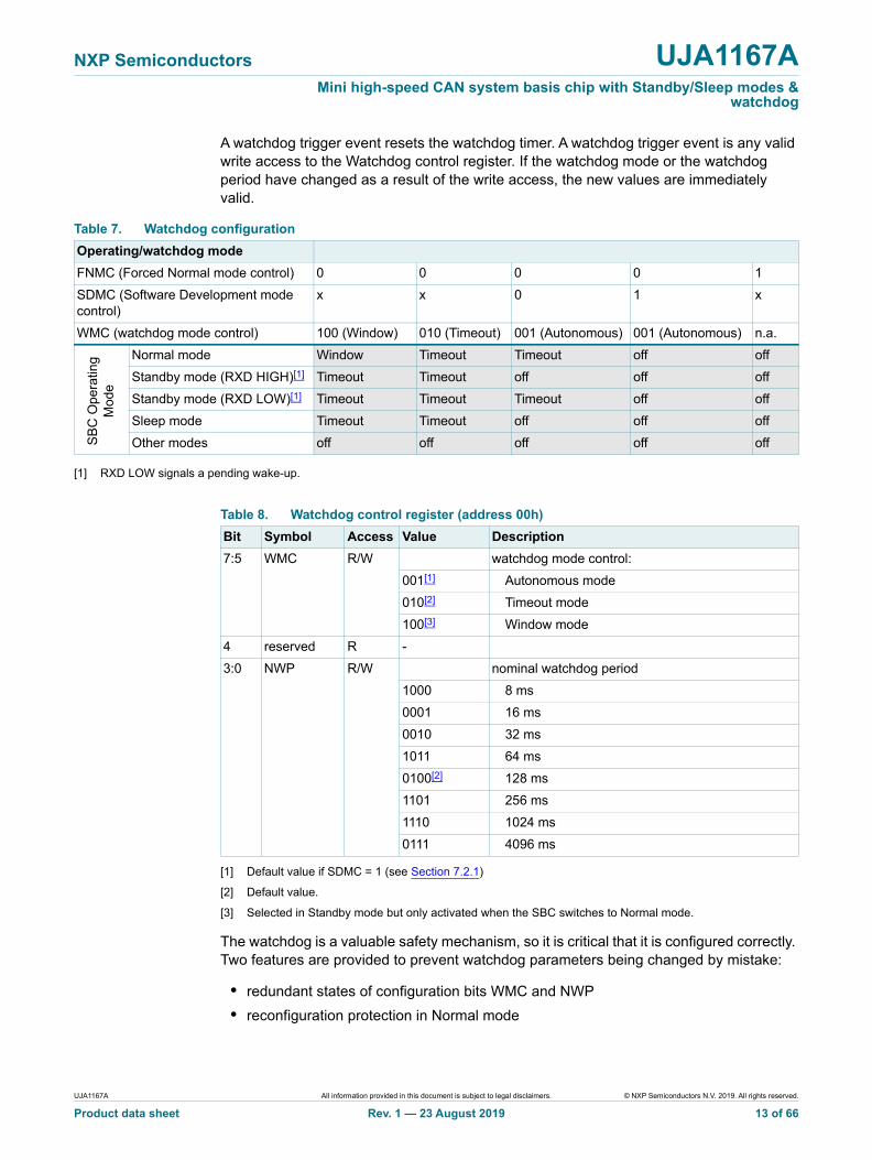
7.2 Watchdog
The UJA1167A contains a watchdog that supports three operating modes: Window, Timeout and Autonomous. In Window mode (available only in SBC Normal mode), a watchdog trigger event within a closed watchdog window resets the watchdog timer. In Timeout mode, the watchdog runs continuously and can be reset at any time within the timeout time by a watchdog trigger. Watchdog timeout mode can also be used for cyclic wake-up of the microcontroller. In Autonomous mode, the watchdog can be off or in Timeout mode (see Section 7.2.4).
The watchdog mode is selected via bits WMC in the Watchdog control register (Table 8). The SBC must be in Standby mode when the watchdog mode and/or period is changed. If Window mode is selected (WMC = 100), the watchdog will remain in (or switch to) Timeout mode until the SBC enters Normal mode. Any attempt to change the watchdog operating mode (via WMC) or period (via NWP) while the SBC is in Normal mode will cause the UJA1167A to switch to Reset mode. The reset source status bits (RSS) will be set to 10000 (‘illegal watchdog mode control access’; see Table 6) and an SPI failure (SPIF) event triggered, if enabled.
Eight watchdog periods are supported, from 8 ms to 4096 ms. The watchdog period is programmed via bits NWP. The selected period is valid for both Window and Timeout modes. The default watchdog period is 128 ms.
Table 6. Main status register (address 03h)
Bit Symbol Access Value Description
7 reserved R -
6 OTWS R overtemperature warning status:
0 IC temperature below overtemperature warning threshold
1 IC temperature above overtemperature warning threshold
5 NMS R Normal mode status:
0 UJA1167A has entered Normal mode (after power-up)
1 UJA1167A has powered up but has not yet switched to Normal mode
4:0 RSS R reset source status:
00000 exited Off mode (power-on)
00001 CAN wake-up in Sleep mode
00100 wake-up via WAKE pin in Sleep mode
01100 watchdog overflow in Sleep mode (Timeout mode)
01101 diagnostic wake-up in Sleep mode
01110 watchdog triggered too early (Window mode)
01111 watchdog overflow (Window mode or Timeout mode with WDF = 1)
10000 illegal watchdog mode control access
10001 RSTN pulled down externally
10010 exited Overtemp mode
10011 V1 undervoltage
10100 illegal Sleep mode command received
UJA1167A All information provided in this document is subject to legal disclaimers. © NXP Semiconductors N.V. 2019. All rights reserved.
Product data sheet Rev. 1 — 23 August 2019 12 of 66
NXP Semiconductors UJA1167AMini high-speed CAN system basis chip with Standby/Sleep modes &
watchdog
A watchdog trigger event resets the watchdog timer. A watchdog trigger event is any valid write access to the Watchdog control register. If the watchdog mode or the watchdog period have changed as a result of the write access, the new values are immediately valid.
[1] RXD LOW signals a pending wake-up.
[1] Default value if SDMC = 1 (see Section 7.2.1)
[2] Default value.
[3] Selected in Standby mode but only activated when the SBC switches to Normal mode.
The watchdog is a valuable safety mechanism, so it is critical that it is configured correctly. Two features are provided to prevent watchdog parameters being changed by mistake:
• redundant states of configuration bits WMC and NWP
• reconfiguration protection in Normal mode
Table 7. Watchdog configuration
Operating/watchdog mode
FNMC (Forced Normal mode control) 0 0 0 0 1
SDMC (Software Development mode control)
x x 0 1 x
WMC (watchdog mode control) 100 (Window) 010 (Timeout) 001 (Autonomous) 001 (Autonomous) n.a.
SB
C O
pera
ting
Mod
e
Normal mode Window Timeout Timeout off off
Standby mode (RXD HIGH)[1] Timeout Timeout off off off
Standby mode (RXD LOW)[1] Timeout Timeout Timeout off off
Sleep mode Timeout Timeout off off off
Other modes off off off off off
Table 8. Watchdog control register (address 00h)
Bit Symbol Access Value Description
7:5 WMC R/W watchdog mode control:
001[1] Autonomous mode
010[2] Timeout mode
100[3] Window mode
4 reserved R -
3:0 NWP R/W nominal watchdog period
1000 8 ms
0001 16 ms
0010 32 ms
1011 64 ms
0100[2] 128 ms
1101 256 ms
1110 1024 ms
0111 4096 ms
UJA1167A All information provided in this document is subject to legal disclaimers. © NXP Semiconductors N.V. 2019. All rights reserved.
Product data sheet Rev. 1 — 23 August 2019 13 of 66

NXP Semiconductors UJA1167AMini high-speed CAN system basis chip with Standby/Sleep modes &
watchdog
Redundant states associated with control bits WMC and NWP ensure that a single bit error cannot cause the watchdog to be configured incorrectly (at least two bits must be changed to reconfigure WMC or NWP). If an attempt is made to write an invalid code to WMC or NWP (e.g. 011 or 1001 respectively), the SPI operation is abandoned and an SPI failure event is captured, if enabled (see Section 7.10).
Two operating modes have a major impact on the operation of the watchdog: Forced Normal mode and Software Development mode (Software Development mode is provided for test purposes and is not an SBC operating mode; the UJA1167A can be in any mode with Software Development mode enabled; see Section 7.2.1). These modes are enabled and disabled via bits FNMC and SDMC respectively in the SBC configuration control register (see Table 9). Note that this register is located in the non-volatile memory area (see Section 7.10). In Forced Normal mode (FNM), the watchdog is completely disabled. In Software Development mode (SDM), the watchdog can be disabled or activated for test purposes.
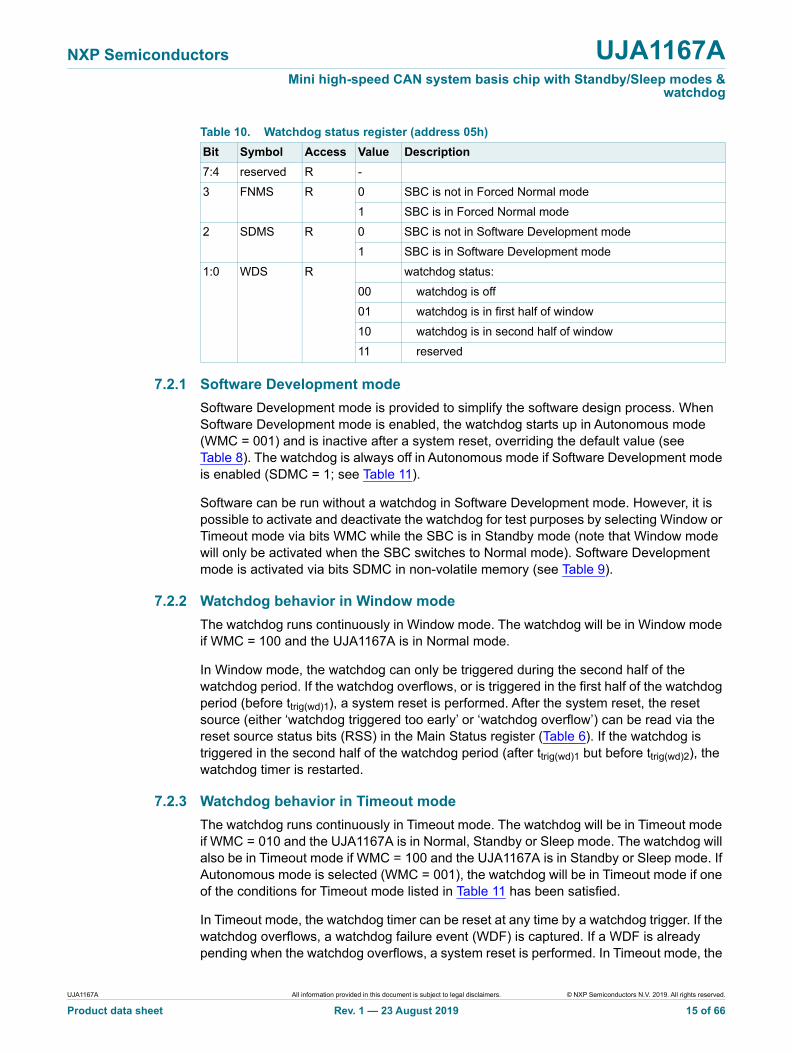
Information on the status of the watchdog is available from the Watchdog status register (Table 10). This register also indicates whether Forced Normal and Software Development modes are active.
[1] Factory preset value.
Table 9. SBC configuration control register (address 74h)
Bit Symbol Access Value Description
7:6 reserved R -
5:4 V1RTSUC R/W V1 reset threshold (defined by bit V1RTC) at start-up:
00[1] V1 undervoltage detection at 90 % of nominal value at start-up (V1RTC = 00)
01 V1 undervoltage detection at 80 % of nominal value at start-up (V1RTC = 01)
10 V1 undervoltage detection at 70 % of nominal value at start-up (V1RTC = 10)
11 V1 undervoltage detection at 60 % of nominal value at start-up (V1RTC = 11)
3 FNMC R/W Forced Normal mode control:
0 Forced Normal mode disabled
1[1] Forced Normal mode enabled
2 SDMC R/W Software Development mode control:
0[1] Software Development mode disabled
1 Software Development mode enabled
1 reserved R -
0 SLPC R/W Sleep control:
0[1] the SBC supports Sleep mode
1 Sleep mode commands will be ignored
UJA1167A All information provided in this document is subject to legal disclaimers. © NXP Semiconductors N.V. 2019. All rights reserved.
Product data sheet Rev. 1 — 23 August 2019 14 of 66
NXP Semiconductors UJA1167AMini high-speed CAN system basis chip with Standby/Sleep modes &
watchdog
7.2.1 Software Development mode
Software Development mode is provided to simplify the software design process. When Software Development mode is enabled, the watchdog starts up in Autonomous mode (WMC = 001) and is inactive after a system reset, overriding the default value (see Table 8). The watchdog is always off in Autonomous mode if Software Development mode is enabled (SDMC = 1; see Table 11).
Software can be run without a watchdog in Software Development mode. However, it is possible to activate and deactivate the watchdog for test purposes by selecting Window or Timeout mode via bits WMC while the SBC is in Standby mode (note that Window mode will only be activated when the SBC switches to Normal mode). Software Development mode is activated via bits SDMC in non-volatile memory (see Table 9).
7.2.2 Watchdog behavior in Window mode
The watchdog runs continuously in Window mode. The watchdog will be in Window mode if WMC = 100 and the UJA1167A is in Normal mode.
In Window mode, the watchdog can only be triggered during the second half of the watchdog period. If the watchdog overflows, or is triggered in the first half of the watchdog period (before ttrig(wd)1), a system reset is performed. After the system reset, the reset source (either ‘watchdog triggered too early’ or ‘watchdog overflow’) can be read via the reset source status bits (RSS) in the Main Status register (Table 6). If the watchdog is triggered in the second half of the watchdog period (after ttrig(wd)1 but before ttrig(wd)2), the watchdog timer is restarted.
7.2.3 Watchdog behavior in Timeout mode
The watchdog runs continuously in Timeout mode. The watchdog will be in Timeout mode if WMC = 010 and the UJA1167A is in Normal, Standby or Sleep mode. The watchdog will also be in Timeout mode if WMC = 100 and the UJA1167A is in Standby or Sleep mode. If Autonomous mode is selected (WMC = 001), the watchdog will be in Timeout mode if one of the conditions for Timeout mode listed in Table 11 has been satisfied.
In Timeout mode, the watchdog timer can be reset at any time by a watchdog trigger. If the watchdog overflows, a watchdog failure event (WDF) is captured. If a WDF is already pending when the watchdog overflows, a system reset is performed. In Timeout mode, the
Table 10. Watchdog status register (address 05h)
Bit Symbol Access Value Description
7:4 reserved R -
3 FNMS R 0 SBC is not in Forced Normal mode
1 SBC is in Forced Normal mode
2 SDMS R 0 SBC is not in Software Development mode
1 SBC is in Software Development mode
1:0 WDS R watchdog status:
00 watchdog is off
01 watchdog is in first half of window
10 watchdog is in second half of window
11 reserved
UJA1167A All information provided in this document is subject to legal disclaimers. © NXP Semiconductors N.V. 2019. All rights reserved.
Product data sheet Rev. 1 — 23 August 2019 15 of 66

NXP Semiconductors UJA1167AMini high-speed CAN system basis chip with Standby/Sleep modes &
watchdog
watchdog can be used as a cyclic wake-up source for the microcontroller when the UJA1167A is in Standby or Sleep mode. In Sleep mode, a watchdog overflow generates a wake-up event.
When the SBC is in Sleep mode with watchdog Timeout mode selected, a wake-up event is generated after the nominal watchdog period (NWP). If bit WDF is set, RXD is forced LOW and V1 is turned on. The application software can then clear the WDF bit and trigger the watchdog before it overflows.
7.2.4 Watchdog behavior in Autonomous mode
Autonomous mode is selected when WMC = 001. In Autonomous mode, the watchdog is either off or in Timeout mode, according to the conditions detailed in Table 11.
When Autonomous mode is selected, the watchdog will be in Timeout mode if the SBC is in Normal mode or Standby mode with RXD LOW, provided Software Development mode has been disabled (SDMC = 0). Otherwise the watchdog will be off.
In Autonomous mode, the watchdog will not be running when the SBC is in Standby (RXD HIGH) or Sleep mode. If a wake-up event is captured, pin RXD is forced LOW to signal the event and the watchdog is automatically restarted in Timeout mode. If the SBC was in Sleep mode when the wake-up event was captured, it switches to Standby mode.
7.3 System reset
When a system reset occurs, the SBC switches to Reset mode and initiates a process that generates a low-level pulse on pin RSTN.
7.3.1 Characteristics of pin RSTN
Pin RSTN is a bidirectional open drain low side driver with integrated pull-up resistance, as shown in Figure 4. With this configuration, the SBC can detect the pin being pulled down externally, e.g. by the microcontroller. The input reset pulse width must be at least tw(rst).
Table 11. Watchdog status in Autonomous mode
UJA1167A operating mode Watchdog status
SDMC = 0 SDMC = 1
Normal Timeout mode off
Standby; RXD HIGH off off
Sleep off off
any other mode off off
Standby; RXD LOW Timeout mode off
UJA1167A All information provided in this document is subject to legal disclaimers. © NXP Semiconductors N.V. 2019. All rights reserved.
Product data sheet Rev. 1 — 23 August 2019 16 of 66

NXP Semiconductors UJA1167AMini high-speed CAN system basis chip with Standby/Sleep modes &
watchdog
7.3.2 Selecting the output reset pulse width
The duration of the output reset pulse is selected via bits RLC in the Start-up control register (Table 12). The SBC distinguishes between a cold start and a warm start. A cold start is performed if the reset event was combined with a V1 undervoltage event (power-on reset, reset during Sleep mode, over-temperature reset, V1 undervoltage before entering or while in Reset mode). The output reset pulse width for a cold start is determined by the setting of bits RLC.
If any other reset event occurs without a V1 undervoltage (external reset, watchdog failure, watchdog change attempt in Normal mode, illegal Sleep mode command) the SBC uses the shortest reset length (tw(rst) = 1 ms to 1.5 ms). This is called a warm start of the microcontroller.
[1] Factory preset value.
7.3.3 Reset sources
The following events will cause the UJA1167A to switch to Reset mode:
• VV1 drops below the selected V1 undervoltage threshold defined by bits V1RTC
• pin RSTN is pulled down externally
• the watchdog overflows in Window mode
• the watchdog is triggered too early in Window mode (before ttrig(wd)1)
Fig 4. RSTN internal pin configuration
RSTN
V1
015aaa276
Table 12. Start-up control register (address 73h)
Bit Symbol Access Value Description
7:6 reserved R -
5:4 RLC R/W RSTN output reset pulse width:
00[1] tw(rst) = 20 ms to 25 ms
01 tw(rst) = 10 ms to 12.5 ms
10 tw(rst) = 3.6 ms to 5 ms
11 tw(rst) = 1 ms to 1.5 ms
3 VEXTSUC R/W VEXT/INH start-up control:
0[1] bits VEXTC set to 00 at power-up
1 bits VEXTC set to 11 at power-up
2:0 reserved R -
UJA1167A All information provided in this document is subject to legal disclaimers. © NXP Semiconductors N.V. 2019. All rights reserved.
Product data sheet Rev. 1 — 23 August 2019 17 of 66

NXP Semiconductors UJA1167AMini high-speed CAN system basis chip with Standby/Sleep modes &
watchdog
• the watchdog overflows in Timeout mode with WDF = 1 (watchdog failure pending)
• an attempt is made to reconfigure the Watchdog control register while the SBC is in Normal mode
• the SBC leaves Off mode
• local or CAN bus wake-up in Sleep mode
• diagnostic wake-up in Sleep mode
• the SBC leaves Overtemp mode
• illegal Sleep mode command received
7.4 Global temperature protection
The temperature of the UJA1167A is monitored continuously, except in Sleep and Off modes. The SBC switches to Overtemp mode if the temperature exceeds the overtemperature protection activation threshold, Tth(act)otp. In addition, pin RSTN is driven LOW and V1, VEXT and the CAN transceiver are switched off. When the temperature drops below the overtemperature protection release threshold, Tth(rel)otp, the SBC switches to Standby mode via Reset mode.
In addition, the UJA1167A provides an overtemperature warning. When the IC temperature rises about the overtemperature warning threshold (Tth(warn)otp), status bit OTWS is set and an overtemperature warning event is captured (OTW = 1).
7.5 Power supplies
7.5.1 Battery supply voltage (VBAT)
The internal circuitry is supplied from the battery via pin BAT. The device needs to be protected against negative supply voltages, e.g. by using an external series diode. If VBAT falls below the power-off detection threshold, Vth(det)poff, the SBC switches to Off mode. However, the microcontroller supply voltage (V1) remains active until VBAT falls below 2 V.
The SBC switches from Off mode to Reset mode tstartup after the battery voltage rises above the power-on detection threshold, Vth(det)pon. Power-on event status bit PO is set to 1 to indicate the UJA1167A has powered up and left Off mode (see Table 21).
7.5.2 Low-drop voltage supply for 5 V microcontroller (V1)
V1 is intended to supply the microcontroller and the internal CAN transceiver and delivers up to 150 mA at 5 V. The output voltage on V1 is monitored. A system reset is generated if the voltage on V1 drops below the selected undervoltage threshold (60 %, 70 %, 80 % or 90 % of the nominal V1 output voltage, selected via V1RTC in the V1 and INH/VEXT control register; see Table 13).
The internal CAN transceiver consumes 50 mA (max) when the bus is continuously dominant, leaving 100 mA available for the external load on pin V1. In practice, the typical current consumption of the CAN transceiver is lower (25 mA), depending on the application, leaving more current available for the load.
The default value of the undervoltage threshold at power-up is determined by the value of bits V1RTSUC in the SBC configuration control register (Table 9). The SBC configuration control register is in non-volatile memory, allowing the user to define the undervoltage threshold (V1RTC) at start-up.
UJA1167A All information provided in this document is subject to legal disclaimers. © NXP Semiconductors N.V. 2019. All rights reserved.
Product data sheet Rev. 1 — 23 August 2019 18 of 66
NXP Semiconductors UJA1167AMini high-speed CAN system basis chip with Standby/Sleep modes &
watchdog
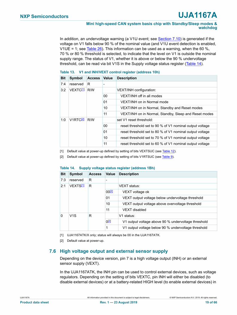
In addition, an undervoltage warning (a V1U event; see Section 7.10) is generated if the voltage on V1 falls below 90 % of the nominal value (and V1U event detection is enabled, V1UE = 1; see Table 26). This information can be used as a warning, when the 60 %, 70 % or 80 % threshold is selected, to indicate that the level on V1 is outside the nominal supply range. The status of V1, whether it is above or below the 90 % undervoltage threshold, can be read via bit V1S in the Supply voltage status register (Table 14).
[1] Default value at power-up defined by setting of bits VEXTSUC (see Table 12).
[2] Default value at power-up defined by setting of bits V1RTSUC (see Table 9).
[1] UJA1167ATK/X only; status will always be 00 in the UJA1167ATK.
[2] Default value at power-up.
7.6 High voltage output and external sensor supply
Depending on the device version, pin 7 is a high voltage output (INH) or an external sensor supply (VEXT).
In the UJA1167ATK, the INH pin can be used to control external devices, such as voltage regulators. Depending on the setting of bits VEXTC, pin INH will either be disabled (to disable external devices) or at a battery-related HIGH level (to enable external devices) in
Table 13. V1 and INH/VEXT control register (address 10h)
Bit Symbol Access Value Description
7:4 reserved R -
3:2 VEXTC[1] R/W VEXT/INH configuration:
00 VEXT/INH off in all modes
01 VEXT/INH on in Normal mode
10 VEXT/INH on in Normal, Standby and Reset modes
11 VEXT/INH on in Normal, Standby, Sleep and Reset modes
1:0 V1RTC[2] R/W set V1 reset threshold:
00 reset threshold set to 90 % of V1 nominal output voltage
01 reset threshold set to 80 % of V1 nominal output voltage
10 reset threshold set to 70 % of V1 nominal output voltage
11 reset threshold set to 60 % of V1 nominal output voltage
Table 14. Supply voltage status register (address 1Bh)
Bit Symbol Access Value Description
7:3 reserved R -
2:1 VEXTS[1] R VEXT status:
00[2] VEXT voltage ok
01 VEXT output voltage below undervoltage threshold
10 VEXT output voltage above overvoltage threshold
11 VEXT disabled
0 V1S R V1 status:
0[2] V1 output voltage above 90 % undervoltage threshold
1 V1 output voltage below 90 % undervoltage threshold
UJA1167A All information provided in this document is subject to legal disclaimers. © NXP Semiconductors N.V. 2019. All rights reserved.
Product data sheet Rev. 1 — 23 August 2019 19 of 66

NXP Semiconductors UJA1167AMini high-speed CAN system basis chip with Standby/Sleep modes &
watchdog
selected SBC operating modes (see Table 13). To ensure external devices are not disabled due to an overtemperature event, pin INH does not change state when the SBC switches to Overtemp mode.
In the UJA1167ATK/X, the VEXT pin is a voltage output intended to supply external components, delivering up to 30 mA at 5 V. Like INH, VEXT is also configured via bits VEXTC in the V1 and INH/VEXT control register (Table 13).
The default value of VEXTC at power-on is defined by bits VEXTSUC in non-volatile memory (see Section 7.11).
In contrast to pin INH, pin VEXT is disabled when the SBC switches to Overtemp mode. The status of VEXT can be read from the Supply voltage status register (Table 14).
7.7 High-speed CAN transceiver
The integrated high-speed CAN transceiver is designed for active communication at bit rates up to 1 Mbit/s, providing differential transmit and receive capability to a CAN protocol controller. The transceiver is ISO 11898-2:2016 compliant. The CAN transmitter is supplied from V1. The UJA1167A includes additional timing parameters on loop delay symmetry to ensure reliable communication in fast phase at data rates up to 5 Mbit/s, as used in CAN FD networks.
The CAN transceiver supports autonomous CAN biasing, which helps to minimize RF emissions. CANH and CANL are always biased to 2.5 V when the transceiver is in Active or Listen-only modes (CMC = 01/10/11).
Autonomous biasing is active in CAN Offline mode - to 2.5 V if there is activity on the bus (CAN Offline Bias mode) and to GND if there is no activity on the bus for t > tto(silence) (CAN Offline mode).
This is useful when the node is disabled due to a malfunction in the microcontroller. The SBC ensures that the CAN bus is correctly biased to avoid disturbing ongoing communication between other nodes. The autonomous CAN bias voltage is derived directly from VBAT.
7.7.1 CAN operating modes
The integrated CAN transceiver supports four operating modes: Active, Listen-only, Offline and Offline Bias (see Figure 5). The CAN transceiver operating mode depends on the UJA1167A operating mode and on the setting of bits CMC in the CAN control register (Table 15).
When the UJA1167A is in Normal mode, the CAN transceiver operating mode (Active, Listen-only or Offline) can be selected via bits CMC in the CAN control register (Table 15). When the UJA1167A is in Standby or Sleep modes, the transceiver is forced to Offline or Offline Bias mode (depending on bus activity).
7.7.1.1 CAN Active mode
In CAN Active mode, the transceiver can transmit and receive data via CANH and CANL. The differential receiver converts the analog data on the bus lines into digital data, which is output on pin RXD. The transmitter converts digital data generated by the CAN controller (input on pin TXD) into analog signals suitable for transmission over the CANH and CANL bus lines.
UJA1167A All information provided in this document is subject to legal disclaimers. © NXP Semiconductors N.V. 2019. All rights reserved.
Product data sheet Rev. 1 — 23 August 2019 20 of 66

NXP Semiconductors UJA1167AMini high-speed CAN system basis chip with Standby/Sleep modes &
watchdog
CAN Active mode is selected when CMC = 01 or 10. When CMC = 01, V1/CAN undervoltage detection is enabled and the transceiver will go to CAN Offline or CAN Offline Bias mode when the voltage on V1 drops below the 90 % threshold. When CMC = 10, V1/CAN undervoltage detection is disabled. The transmitter will remain active until the voltage on V1 drops below the V1 reset threshold (selected via bits V1RTC). The SBC will then switch to Reset mode and the transceiver will switch to CAN Offline or CAN Offline Bias mode.
The CAN transceiver is in Active mode when:
• the UJA1167A is in Normal mode (MC = 111) and the CAN transceiver has been enabled by setting bits CMC in the CAN control register to 01 or 10 (see Table 15) and:
– if CMC = 01, the voltage on pin V1 is above the 90 % undervoltage threshold
– if CMC = 10, the voltage on pin V1 is above the V1 reset threshold
If pin TXD is held LOW (e.g. by a short-circuit to GND) when CAN Active mode is selected via bits CMC, the transceiver will not enter CAN Active mode but will switch to or remain in CAN Listen-only mode. It will remain in Listen-only mode until pin TXD goes HIGH in order to prevent a hardware and/or software application failure from driving the bus lines to an unwanted dominant state.
In CAN Active mode, the CAN bias voltage is derived from V1.
The application can determine whether the CAN transceiver is ready to transmit/receive data or is disabled by reading the CAN Transceiver Status (CTS) bit in the Transceiver Status Register (Table 16).
7.7.1.2 CAN Listen-only mode
CAN Listen-only mode allows the UJA1167A to monitor bus activity while the transceiver is inactive, without influencing bus levels. This facility could be used by development tools that need to listen to the bus but do not need to transmit or receive data or for software-driven selective wake-up. Dedicated microcontrollers could be used for selective wake-up, providing an embedded low-power CAN engine designed to monitor the bus for potential wake-up events.
In Listen-only mode the CAN transmitter is disabled, reducing current consumption. The CAN receiver and CAN biasing remain active. This enables the host microcontroller to switch to a low-power mode in which an embedded CAN protocol controller remains active, waiting for a signal to wake up the microcontroller.
The CAN transceiver is in Listen-only mode when:
• the UJA1167A is in Normal mode and CMC = 11
The CAN transceiver will not leave Listen-only mode while TXD is LOW or CAN Active mode is selected with CMC = 01 while the voltage on V1 is below the 90 % undervoltage threshold.
7.7.1.3 CAN Offline and Offline Bias modes
In CAN Offline mode, the transceiver monitors the CAN bus for a wake-up event, provided CAN wake-up detection is enabled (CWE = 1). CANH and CANL are biased to GND.
UJA1167A All information provided in this document is subject to legal disclaimers. © NXP Semiconductors N.V. 2019. All rights reserved.
Product data sheet Rev. 1 — 23 August 2019 21 of 66

NXP Semiconductors UJA1167AMini high-speed CAN system basis chip with Standby/Sleep modes &
watchdog
CAN Offline Bias mode is the same as CAN Offline mode, with the exception that the CAN bus is biased to 2.5 V. This mode is activated automatically when activity is detected on the CAN bus while the transceiver is in CAN Offline mode. The transceiver will return to CAN Offline mode if the CAN bus is silent (no CAN bus edges) for longer than tto(silence).
The CAN transceiver switches to CAN Offline mode from CAN Active mode or CAN Listen-only mode if:
• the SBC switches to Reset or Standby or Sleep mode OR
• the SBC is in Normal mode and CMC = 00
provided the CAN-bus has been inactive for at least tto(silence). If the CAN-bus has been inactive for less than tto(silence), the CAN transceiver switches first to CAN Offline Bias mode and then to CAN Offline mode once the bus has been silent for tto(silence).
The CAN transceiver switches to CAN Offline/Offline Bias mode from CAN Active mode if CMC = 01 and the voltage on V1 drops below the 90 % undervoltage threshold or CMC = 10 and the voltage on V1 drops below the V1 reset threshold.
The CAN transceiver switches to CAN Offline mode:
• from CAN Offline Bias mode if no activity is detected on the bus (no CAN edges) for t > tto(silence) OR
• when the SBC switches from Off or Overtemp mode to Reset mode
The CAN transceiver switches from CAN Offline mode to CAN Offline Bias mode if:
• a standard wake-up pattern is detected on the CAN bus OR
• the SBC is in Normal mode, CMC = 01 or 10 and VV1 < 90 %
7.7.1.4 CAN Off mode
The CAN transceiver is switched off completely with the bus lines floating when:
• the SBC switches to Off or Overtemp mode OR
• VBAT falls below the CAN receiver undervoltage detection threshold, Vuvd(CAN)
It will be switched on again on entering CAN Offline mode when VBAT rises above the undervoltage recovery threshold (Vuvr(CAN)) and the SBC is no longer in Off/Overtemp mode. CAN Off mode prevents reverse currents flowing from the bus when the battery supply to the SBC is lost.
UJA1167A All information provided in this document is subject to legal disclaimers. © NXP Semiconductors N.V. 2019. All rights reserved.
Product data sheet Rev. 1 — 23 August 2019 22 of 66

NXP Semiconductors UJA1167AMini high-speed CAN system basis chip with Standby/Sleep modes &
watchdog
7.7.2 CAN standard wake-up
If the CAN transceiver is in Offline mode and CAN wake-up is enabled (CWE = 1), the UJA1167A will monitor the bus for a wake-up pattern.
A filter at the receiver input prevents unwanted wake-up events occurring due to automotive transients or EMI. A dominant-recessive-dominant wake-up pattern must be transmitted on the CAN bus within the wake-up timeout time (tto(wake)) to pass the wake-up filter and trigger a wake-up event (see Figure 6; note that additional pulses may occur between the recessive/dominant phases). The recessive and dominant phases must last at least twake(busrec) and twake(busdom), respectively.
(1) To prevent the bus lines being driven to a permanent dominant state, the transceiver will not switch to CAN Active mode or CAN Listen-only mode if pin TXD is held LOW (e.g. by a short-circuit to GND)
Fig 5. CAN transceiver state machine (with FNMC = 0)
CAN Active
015aaa284
CAN Listen-onlytransmitter: off
RXD: wake-up/intCANH/CANL: terminated
to 2.5 V (from VBAT)
CAN Offline Bias
CAN Offline
CAN Off
leaving Off/Overtemp &VBAT > Vuvr(CAN)
from all modes
Off OROvertemp OR
VBAT < Vuvd(CAN)
[Reset OR StandbyOR Sleep OR
(Normal & CMC = 00) OR (CMC = 01 & V V1 < 90 %)]
& t > tto(silence)
Normal & CMC = 11
Normal & (CMC = 01 OR CMC = 10) &
VV1 > 90 %(1)
Normal & CMC = 11
[Reset OR Standby OR Sleep OR(Normal & CMC = 00)]
& t < tto(silence)
[Reset or Standby or Sleep OR(Nomal & CMC = 00)]
& t > tto(silence)
Normal & (CMC = 01 ORCMC = 10) &
VV1 > 90 %(1)
CAN bus wake-up OR[Normal & (CMC = 01 OR CMC = 10) &
VV1 < 90 %]
Normal & CMC = 11
Normal &(CMC = 01 OR CMC = 10) &
VV1 < 90 %
transmitter: onRXD: bitstream
CANH/CANL: terminatedto V1/2 (≈2.5 V)
Normal & (CMC = 01 OR CMC = 10) &
VV1 > 90 %(1)
[Reset OR StandbyOR Sleep OR
(Normal & CMC = 00) OR (CMC = 01 & V V1 < 90 %)]
& t < tto(silence)
[Reset OR Standby OR Sleep OR(Normal & CMC = 00)]
& t > tto(silence)
transmitter: offRXD: bitstream
CANH/CANL: terminatedto 2.5 V (from VBAT)
transmitter: offRXD: wake-up/int
CANH/CANL: terminatedto GND
transmitter: offRXD: wake-up/int
CANH/CANL: floating
UJA1167A All information provided in this document is subject to legal disclaimers. © NXP Semiconductors N.V. 2019. All rights reserved.
Product data sheet Rev. 1 — 23 August 2019 23 of 66

NXP Semiconductors UJA1167AMini high-speed CAN system basis chip with Standby/Sleep modes &
watchdog
When a valid CAN wake-up pattern is detected on the bus, wake-up bit CW in the Transceiver event status register is set (see Table 23) and pin RXD is driven LOW. If the SBC was in Sleep mode when the wake-up pattern was detected, V1 is enabled to supply the microcontroller and the SBC switches to Standby mode via Reset mode.
7.7.3 CAN control and Transceiver status registers
[1] Only active when CMC = 01.
Fig 6. CAN wake-up timing
twake(busdom)
CANH
CANL
VO(dif)
RXD
≤ tto(wake)bus
aaa-021858
twake(busdom) twake(busrec)
Table 15. CAN control register (address 20h)
Bit Symbol Access Value Description
7:2 reserved R/W -
1:0 CMC R/W CAN transceiver operating mode selection (available when UJA1167A is in Normal mode; MC = 111):
00 Offline mode
01 Active mode; see Section 7.7.1.1 and Section 7.7.1.3
10 Active mode; see Section 7.7.1.1 and Section 7.7.1.3
11 Listen-only mode
Table 16. Transceiver status register (address 22h)
Bit Symbol Access Value Description
7 CTS R 0 CAN transceiver not in Active mode
1 CAN transceiver in Active mode
6:4 reserved R -
3 CBSS R 0 CAN bus active (communication detected on bus)
1 CAN bus inactive (for longer than tto(silence))
2 reserved R -
1 VCS[1] R 0 the output voltage on V1 is above the 90 % threshold
1 the output voltage on V1 is below the 90 % threshold
0 CFS R 0 no TXD dominant timeout event detected
1 CAN transmitter disabled due to a TXD dominant timeout event
UJA1167A All information provided in this document is subject to legal disclaimers. © NXP Semiconductors N.V. 2019. All rights reserved.
Product data sheet Rev. 1 — 23 August 2019 24 of 66

NXP Semiconductors UJA1167AMini high-speed CAN system basis chip with Standby/Sleep modes &
watchdog
7.8 CAN fail-safe features
7.8.1 TXD dominant timeout
A TXD dominant time-out timer is started when pin TXD is forced LOW while the transceiver is in CAN Active Mode. If the LOW state on pin TXD persists for longer than the TXD dominant time-out time (tto(dom)TXD), the transmitter is disabled, releasing the bus lines to recessive state. This function prevents a hardware and/or software application failure from driving the bus lines to a permanent dominant state (blocking all network communications). The TXD dominant time-out timer is reset when pin TXD goes HIGH. The TXD dominant time-out time also defines the minimum possible bit rate of 4.4 kbit/s.
When the TXD dominant time-out time is exceeded, a CAN failure event is captured (CF = 1; see Table 23), if enabled (CFE = 1; see Table 27). In addition, the status of the TXD dominant timeout can be read via the CFS bit in the Transceiver status register (Table 16) and bit CTS is cleared.
7.8.2 Pull-up on TXD pin
Pin TXD has an internal pull-up towards V1 to ensure a safe defined recessive driver state in case the pin is left floating.
7.8.3 V1 undervoltage event
When CMC = 01, a CAN failure event is captured (CF = 1) and status bit VCS is set to 1 when the supply to the CAN transceiver (VV1) falls below 90 % of its nominal value (assuming CAN failure detection is enabled; CFE = 1).
7.8.4 Loss of power at pin BAT
A loss of power at pin BAT has no influence on the bus lines or on the microcontroller. No reverse currents will flow from the bus.
7.9 Local wake-up via WAKE pin
Local wake-up is enabled via bits WPRE and WPFE in the WAKE pin event capture enable register (see Table 28). A wake-up event is triggered by a LOW-to-HIGH (if WPRE = 1) and/or a HIGH-to-LOW (if WPFE = 1) transition on the WAKE pin. This arrangement allows for maximum flexibility when designing a local wake-up circuit. In applications that don’t make use of the local wake-up facility, local wake-up should be disabled and the WAKE pin connected to GND to ensure optimal EMI performance.
While the SBC is in Normal mode, the status of the voltage on pin WAKE can always be read via bit WPVS. Otherwise, WPVS is only valid if local wake-up is enabled (WPRE = 1 and/or WPFE = 1).
Table 17. WAKE status register (address 4Bh)
Bit Symbol Access Value Description
7:2 reserved R -
1 WPVS R WAKE pin status:
0 voltage on WAKE pin below switching threshold (Vth(sw))
1 voltage on WAKE pin above switching threshold (Vth(sw))
0 reserved R -
UJA1167A All information provided in this document is subject to legal disclaimers. © NXP Semiconductors N.V. 2019. All rights reserved.
Product data sheet Rev. 1 — 23 August 2019 25 of 66

NXP Semiconductors UJA1167AMini high-speed CAN system basis chip with Standby/Sleep modes &
watchdog
7.10 Wake-up and interrupt event diagnosis via pin RXD
Wake-up and interrupt event diagnosis in the UJA1167A is intended to provide the microcontroller with information on the status of a range of features and functions. This information is stored in the event status registers (Table 21 to Table 23) and is signaled on pin RXD, if enabled.
A distinction is made between regular wake-up events and interrupt events (at least one regular wake-up source must be enabled to allow the UJA1167A to switch to Sleep mode; see Section 7.1.1.3).
[1] UJA1167ATK/X only.
PO and WDF interrupts are always captured. Wake-up and interrupt detection can be enabled/disabled for the remaining events individually via the event capture enable registers (Table 25 to Table 27).
Table 18. Regular events
Symbol Event Power-on Description
CW CAN wake-up disabled a CAN wake-up event was detected while the transceiver was in CAN Offline mode.
WPR rising edge on WAKE pin
disabled a rising-edge wake-up was detected on pin WAKE
WPF falling edge on WAKE pin
disabled a falling-edge wake-up was detected on pin WAKE
Table 19. Diagnostic events
Symbol Event Power-on Description
PO power-on always enabled
the UJA1167A has exited Off mode (after battery power has been restored/connected)
OTW overtemperature warning disabled the IC temperature has exceeded the overtemperature warning threshold (not in Sleep mode)
SPIF SPI failure disabled SPI clock count error (only 16-, 24- and 32-bit commands are valid), illegal WMC, NWP or MC code or attempted write access to locked register (not in Sleep mode)
WDF watchdog failure always enabled
watchdog overflow in Window or Timeout mode or watchdog triggered too early in Window mode; a system reset is triggered immediately in response to a watchdog failure in Window mode; when the watchdog overflows in Timeout mode, a system reset is only performed if a WDF is already pending (WDF = 1)
VEXTO[1] VEXT overvoltage disabled VEXT overvoltage detected
VEXTU[1] VEXT undervoltage disabled VEXT undervoltage detected
V1U V1 undervoltage disabled voltage on V1 has dropped below the 90 % undervoltage threshold when V1 is active (event is not captured in Sleep mode because V1 is off). V1U event capture is independent of the setting of bits V1RTC.
CBS CAN bus silence disabled no activity on CAN bus for tto(silence) (detected only when CBSE = 1 while bus active)
CF CAN failure disabled one of the following CAN failure events detected:
- CAN transceiver deactivated due to a V1 undervoltage
- CAN transceiver deactivated due to a dominant clamped TXD (not in Sleep mode)
UJA1167A All information provided in this document is subject to legal disclaimers. © NXP Semiconductors N.V. 2019. All rights reserved.
Product data sheet Rev. 1 — 23 August 2019 26 of 66

NXP Semiconductors UJA1167AMini high-speed CAN system basis chip with Standby/Sleep modes &
watchdog
If an event occurs while the associated event capture function is enabled, the relevant event status bit is set. If the transceiver is in CAN Offline mode with V1 active (SBC Normal or Standby mode), pin RXD is forced LOW to indicate that a wake-up or interrupt event has been detected. If the UJA1167A is in sleep mode when the event occurs, the microcontroller supply, V1, is activated and the SBC switches to Standby mode (via Reset mode).
The microcontroller can monitor events via the event status registers. An extra status register, the Global event status register (Table 20), is provided to help speed up software polling routines. By polling the Global event status register, the microcontroller can quickly determine the type of event captured (system, supply, transceiver or WAKE pin) and then query the relevant table (Table 21, Table 22, Table 23 or Table 24 respectively).
After the event source has been identified, the status flag should be cleared (set to 0) by writing 1 to the relevant bit (writing 0 will have no effect). A number of status bits can be cleared in a single write operation by writing 1 to all relevant bits.
It is strongly recommended to clear only the status bits that were set to 1 when the status registers were last read. This precaution ensures that events triggered just before the write access are not lost.
7.10.1 Interrupt/wake-up delay
If interrupt or wake-up events occur very frequently while the transceiver is in CAN Offline mode, they can have a significant impact on the software processing time (because pin RXD is repeatedly driven LOW, requiring a response from the microcontroller each time an interrupt/wake-up is generated). The UJA1167A incorporates an event delay timer to limit the disturbance to the software.
When one of the event capture status bits is cleared, pin RXD is released (HIGH) and a timer is started. If further events occur while the timer is running, the relevant status bits are set. If one or more events are pending when the timer expires after td(event), pin RXD goes LOW again to alert the microcontroller.
In this way, the microcontroller is interrupted once to process a number of events rather than several times to process individual events.
If all events are cleared while the timer is running, RXD remains HIGH after the timer expires, since there are no pending events. The event capture registers can be read at any time.
The event capture delay timer is stopped immediately when pin RSTN goes low (triggered by a HIGH-to-LOW transition on the pin). RSTN is driven LOW when the SBC enters Reset, Sleep, Overtemp and Off modes. A pending event is signaled on pin RXD when the SBC enters Sleep mode.
7.10.2 Sleep mode protection
The wake-up event capture function is critical when the UJA1167A is in Sleep mode, because the SBC will only leave Sleep mode in response to a captured wake-up event. To avoid potential system deadlocks, the SBC distinguishes between regular and diagnostic events (see Section 7.10). Wake-up events (via the CAN bus or the WAKE pin) are classified as regular events; diagnostic events signal failure/error conditions or state
UJA1167A All information provided in this document is subject to legal disclaimers. © NXP Semiconductors N.V. 2019. All rights reserved.
Product data sheet Rev. 1 — 23 August 2019 27 of 66

NXP Semiconductors UJA1167AMini high-speed CAN system basis chip with Standby/Sleep modes &
watchdog
changes. At least one regular wake-up event must be enabled before the UJA1167A can switch to Sleep mode. Any attempt to enter Sleep mode while all regular wake-up events are disabled will trigger a system reset.
Another condition that must be satisfied before the UJA1167A can switch to Sleep mode is that all event status bits must be cleared. If an event is pending when the SBC receives a Sleep mode command (MC = 001), it will immediately switch to Reset mode. This condition applies to both regular and diagnostic events.
Sleep mode can be permanently disabled in applications where, for safety reasons, the supply voltage to the host controller must never be cut off. Sleep mode is permanently disabled by setting the Sleep control bit (SLPC) in the SBC configuration register (see Table 9) to 1. This register is located in the non-volatile memory area of the device. When SLPC = 1, a Sleep mode SPI command (MC = 001) will trigger an SPI failure event instead of a transition to Sleep mode.
7.10.3 Event status and event capture registers
After an event source has been identified, the status flag should be cleared (set to 0) by writing 1 to the relevant status bit (writing 0 will have no effect).
Table 20. Global event status register (address 60h)
Bit Symbol Access Value Description
7:4 reserved R -
3 WPE R 0 no pending WAKE pin event
1 WAKE pin event pending at address 0x64
2 TRXE R 0 no pending transceiver event
1 transceiver event pending at address 0x63
1 SUPE R 0 no pending supply event
1 supply event pending at address 0x62
0 SYSE R 0 no pending system event
1 system event pending at address 0x61
Table 21. System event status register (address 61h)
Bit Symbol Access Value Description
7:5 reserved R -
4 PO R/W 0 no recent power-on
1 the UJA1167A has left Off mode after power-on
3 reserved R -
2 OTW R/W 0 overtemperature not detected
1 the global chip temperature has exceeded the overtemperature warning threshold (Tth(warn)otp)
1 SPIF R/W 0 no SPI failure detected
1 SPI failure detected
0 WDF R/W 0 no watchdog failure event captured
1 watchdog failure event captured
UJA1167A All information provided in this document is subject to legal disclaimers. © NXP Semiconductors N.V. 2019. All rights reserved.
Product data sheet Rev. 1 — 23 August 2019 28 of 66

NXP Semiconductors UJA1167AMini high-speed CAN system basis chip with Standby/Sleep modes &
watchdog
[1] UJA1167ATK/X only; reserved in the UJA1167ATK.
Table 22. Supply event status register (address 62h)
Bit Symbol Access Value Description
7:3 reserved R -
2 VEXTO[1] R/W 0 no VEXT overvoltage event captured
1 VEXT overvoltage event captured
1 VEXTU[1] R/W 0 no VEXT undervoltage event captured
1 VEXT undervoltage event captured
0 V1U R/W 0 no V1 undervoltage event captured
1 V1 undervoltage event captured
Table 23. Transceiver event status register (address 63h)
Bit Symbol Access Value Description
7:5 reserved R -
4 CBS R/W 0 CAN bus active
1 no activity on CAN bus for tto(silence)
3:2 reserved R -
1 CF R/W 0 no CAN failure detected
1 (CMC = 01 & CAN transceiver deactivated due to V1 undervoltage) OR dominant clamped TXD
0 CW R/W 0 no CAN wake-up event detected
1 CAN wake-up event detected while the transceiver is in CAN Offline Mode
Table 24. WAKE pin event capture status register (address 64h)
Bit Symbol Access Value Description
7:2 reserved R -
1 WPR R/W 0 no rising edge detected on WAKE pin
1 rising edge detected on WAKE pin
0 WPF R/W 0 no falling edge detected on WAKE pin
1 falling edge detected on WAKE pin
Table 25. System event capture enable register (address 04h)
Bit Symbol Access Value Description
7:3 reserved R -
2 OTWE R/W overtemperature warning event capture:
0 overtemperature warning disabled
1 overtemperature warning enabled
1 SPIFE R/W SPI failure detection:
0 SPI failure detection disabled
1 SPI failure detection enabled
0 reserved R -
UJA1167A All information provided in this document is subject to legal disclaimers. © NXP Semiconductors N.V. 2019. All rights reserved.
Product data sheet Rev. 1 — 23 August 2019 29 of 66

NXP Semiconductors UJA1167AMini high-speed CAN system basis chip with Standby/Sleep modes &
watchdog
[1] UJA1167ATK/X only; reserved in the UJA1167ATK.
Table 26. Supply event capture enable register (address 1Ch)
Bit Symbol Access Value Description
7:3 reserved R -
2 VEXTOE[1] R/W VEXT overvoltage detection:
0 VEXT overvoltage detection disabled
1 VEXT overvoltage detection enabled
1 VEXTUE[1] R/W VEXT undervoltage detection:
0 VEXT undervoltage detection disabled
1 VEXT undervoltage detection enabled
0 V1UE R/W V1 undervoltage detection:
0 V1 undervoltage detection disabled
1 V1 undervoltage detection enabled
Table 27. Transceiver event capture enable register (address 23h)
Bit Symbol Access Value Description
7:5 reserved R -
4 CBSE R/W CAN bus silence detection:
0 CAN bus silence detection disabled
1 CAN bus silence detection enabled
3:2 reserved R -
1 CFE R/W CAN failure detection
0 CAN failure detection disabled
1 CAN failure detection enabled
0 CWE R/W CAN wake-up detection:
0 CAN wake-up detection disabled
1 CAN wake-up detection enabled
Table 28. WAKE pin event capture enable register (address 4Ch)
Bit Symbol Access Value Description
7:2 reserved R -
1 WPRE R/W rising-edge detection on WAKE pin:
0 rising-edge detection on WAKE pin disabled
1 rising-edge detection on WAKE pin enabled
0 WPFE R/W falling-edge detection on WAKE pin:
0 falling-edge detection on WAKE pin disabled
1 falling-edge detection on WAKE pin enabled
UJA1167A All information provided in this document is subject to legal disclaimers. © NXP Semiconductors N.V. 2019. All rights reserved.
Product data sheet Rev. 1 — 23 August 2019 30 of 66

NXP Semiconductors UJA1167AMini high-speed CAN system basis chip with Standby/Sleep modes &
watchdog
7.11 Non-volatile SBC configuration
The UJA1167A contains Multiple Time Programmable Non-Volatile (MTPNV) memory cells that allow some of the default device settings to be reconfigured. The MTPNV memory address range is from 0x73 to 0x74. An overview of the MTPNV registers is given in Table 29.
7.11.1 Programming MTPNV cells
The UJA1167A must be in Forced Normal mode and the MTPNV cells must contain the factory preset values before the non-volatile memory can be reprogrammed. The UJA1167A will switch to Forced Normal mode after a reset event (e.g. pin RSTN LOW) when the MTPNV cells contain the factory preset values (since FNMC = 1).
The factory presets may need to be restored before reprogramming can begin (see Section 7.11.2). When the factory presets have been restored, a system reset is generated automatically and UJA1167A switches to Forced Normal mode. This ensures that the programming cycle cannot be interrupted by the watchdog.
Programming of the non-volatile memory registers is performed in two steps. First, the required values are written to addresses 0x73 and 0x74. In the second step, reprogramming is confirmed by writing the correct CRC value to the MTPNV CRC control register (see Section 7.11.1.1). The SBC starts reprogramming the MTPNV cells as soon as the CRC value has been validated. If the CRC value is not correct, reprogramming is aborted. On completion, a system reset is generated to indicate that the MTPNV cells have been reprogrammed successfully. Note that the MTPNV cells cannot be read while they are being reprogrammed.
After an MTPNV programming cycle has been completed, the non-volatile memory is protected from being overwritten via a standard SPI write operation.
The MTPNV cells can be reprogrammed a maximum of 200 times (Ncy(W)MTP; see Table 47). Bit NVMPS in the MTPNV status register (Table 30) indicates whether the non-volatile cells can be reprogrammed. This register also contains a write counter, WRCNTS, that is incremented each time the MTPNV cells are reprogrammed (up to a maximum value of 111111; there is no overflow; performing a factory reset also increments the counter). This counter is provided for information purposes only; reprogramming will not be rejected when it reaches its maximum value.
An error correction code status bit, ECCS, is set to indicate that the CRC check mechanism in the SBC has detected a single bit failure in non-volatile memory. If more than one bit failure is detected, the SBC will not restart after MTPNV reprogramming. Check the ECCS flag at the end of the production cycle to verify the content of non-volatile memory. When this flag is set, it indicates a device or ECU failure.
Table 29. Overview of MTPNV registers
Address Register Name Bit:
7 6 5 4 3 2 1 0
0x73 Start-up control(see Table 12)
reserved RLC VEXTSUC reserved
0x74 SBC configuration control (see Table 9)
reserved V1RTSUC FNMC SDMC reserved SLPC
UJA1167A All information provided in this document is subject to legal disclaimers. © NXP Semiconductors N.V. 2019. All rights reserved.
Product data sheet Rev. 1 — 23 August 2019 31 of 66

NXP Semiconductors UJA1167AMini high-speed CAN system basis chip with Standby/Sleep modes &
watchdog
[1] Factory preset value.
7.11.1.1 Calculating the CRC value for MTP programming
The cyclic redundancy check value stored in bits CRCC in the MTPNV CRC control register is calculated using the data written to registers 0x73 and 0x74.
The CRC value is calculated using the data representation shown in Figure 7 and the modulo-2 division with the generator polynomial: X8 + X5 + X3 + X2 + X + 1. The result of this operation must be bitwise inverted.
The following parameters can be used to calculate the CRC value (e.g. via the Autosar method):
Alternatively, the following algorithm can be used:
data = 0 // unsigned bytecrc = 0xFF
Table 30. MTPNV status register (address 70h)
Bit Symbol Access Value Description
7:2 WRCNTS R write counter status:
xxxxxx contains the number of times the MTPNV cells were reprogrammed
1 ECCS R error correction code status:
0 no bit failure detected in non-volatile memory
1 bit failure detected and corrected in non-volatile memory
0 NVMPS R non-volatile memory programming status:
0 MTPNV memory cannot be overwritten
1[1] MTPNV memory is ready to be reprogrammed
Table 31. MTPNV CRC control register (address 75h)
Bit Symbol Access Value Description
7:0 CRCC R/W - CRC control data
Fig 7. Data representation for CRC calculation
Table 32. Parameters for CRC coding
Parameter Value
CRC result width 8 bits
Polynomial 0x2F
Initial value 0xFF
Input data reflected no
Result data reflected no
XOR value 0xFF
7 6 01
register 0x73
7 6 01
register 0x74 015aaa382
UJA1167A All information provided in this document is subject to legal disclaimers. © NXP Semiconductors N.V. 2019. All rights reserved.
Product data sheet Rev. 1 — 23 August 2019 32 of 66

NXP Semiconductors UJA1167AMini high-speed CAN system basis chip with Standby/Sleep modes &
watchdog
for i = 0 to 1data = content_of_address(0x73 + i) EXOR crcfor j = 0 to 7
if data 128data = data * 2 // shift left by 1data = data EXOR 0x2F
elsedata = data * 2 // shift left by 1
next jcrc = data
next icrc = crc EXOR 0xFF
7.11.2 Restoring factory preset values
Factory preset values are restored if the following conditions apply for at least td(MTPNV) during power-up:
• pin RSTN is held LOW
• CANH is pulled up to VBAT
• CANL is pulled down to GND
After the factory preset values have been restored, the SBC performs a system reset and enters Forced normal Mode. Since the CAN bus is clamped dominant, pin RXDC is forced LOW. During the factory preset restore process, this pin is forced HIGH; a falling edge on this pin caused by bit PO being set after power-on then clearly indicates that the process has been completed.
Note that the write counter, WRCNTS, in the MTPNV status register is incremented every time the factory presets are restored.
7.12 Device ID
A byte is reserved at address 0x7E for a UJA1167A identification code.
7.13 Lock control register
Sections of the register address area can be write-protected to protect against unintended modifications. Note that this facility only protects locked bits from being modified via the SPI and will not prevent the UJA1167A updating status registers etc.
Table 33. Identification register (address 7Eh)
Bit Symbol Access Value Description
7:0 IDS[7:0] R D8h device identification code - UJA1167ATK
C8h device identification code -UJA1167ATK/X
Table 34. Lock control register (address 0Ah)
Bit Symbol Access Value Description
7 reserved R - cleared for future use
6 LK6C R/W lock control 6: address area 0x68 to 0x6F
0 SPI write-access enabled
1 SPI write-access disabled
UJA1167A All information provided in this document is subject to legal disclaimers. © NXP Semiconductors N.V. 2019. All rights reserved.
Product data sheet Rev. 1 — 23 August 2019 33 of 66

NXP Semiconductors UJA1167AMini high-speed CAN system basis chip with Standby/Sleep modes &
watchdog
7.14 General purpose memory
UJA1167A allocates 4 bytes of RAM as general purpose registers for storing user information. The general purpose registers can be accessed via the SPI at address 0x06 to 0x09 (see Table 35).
7.15 SPI
7.15.1 Introduction
The Serial Peripheral Interface (SPI) provides the communication link with the microcontroller, supporting multi-slave operations. The SPI is configured for full duplex data transfer, so status information is returned when new control data is shifted in. The interface also offers a read-only access option, allowing registers to be read back by the application without changing the register content.
The SPI uses four interface signals for synchronization and data transfer:
• SCSN: SPI chip select; active LOW
• SCK: SPI clock; default level is LOW due to low-power concept (pull-down)
• SDI: SPI data input
• SDO: SPI data output; floating when pin SCSN is HIGH
Bit sampling is performed on the falling edge of the clock and data is shifted in/out on the rising edge, as illustrated in Figure 8.
5 LK5C R/W lock control 5: address area 0x50 to 0x5F
0 SPI write-access enabled
1 SPI write-access disabled
4 LK4C R/W lock control 4: address area 0x40 to 0x4F - WAKE pin control
0 SPI write-access enabled
1 SPI write-access disabled
3 LK3C R/W lock control 3: address area 0x30 to 0x3F
0 SPI write-access enabled
1 SPI write-access disabled
2 LK2C R/W lock control 2: address area 0x20 to 0x2F - transceiver control
0 SPI write-access enabled
1 SPI write-access disabled
1 LK1C R/W lock control 1: address area 0x10 to 0x1F - regulator control
0 SPI write-access enabled
1 SPI write-access disabled
0 LK0C R/W lock control 0: address area 0x06 to 0x09 - general purpose memory
0 SPI write-access enabled
1 SPI write-access disabled
Table 34. Lock control register (address 0Ah)
Bit Symbol Access Value Description
UJA1167A All information provided in this document is subject to legal disclaimers. © NXP Semiconductors N.V. 2019. All rights reserved.
Product data sheet Rev. 1 — 23 August 2019 34 of 66

NXP Semiconductors UJA1167AMini high-speed CAN system basis chip with Standby/Sleep modes &
watchdog
The SPI data in the UJA1167A is stored in a number of dedicated 8-bit registers. Each register is assigned a unique 7-bit address. Two bytes must be transmitted to the SBC for a single register write operation. The first byte contains the 7-bit address along with a ‘read-only’ bit (the LSB). The read-only bit must be 0 to indicate a write operation (if this bit is 1, a read operation is assumed and any data on the SDI pin is ignored). The second byte contains the data to be written to the register.
24- and 32-bit read and write operations are also supported. The register address is automatically incremented, once for a 24-bit operation and twice for a 32-bit operation, as illustrated in Figure 9.
During an SPI data read or write operation, the contents of the addressed register(s) is returned via pin SDO.
Fig 8. SPI timing protocol
SCSN
SCK 01
sampled
floating floating
015aaa255
X
X
MSB MSB-1 MSB-2 MSB-3 LSB+1 LSB
MSB MSB-1 MSB-2 MSB-3 LSB+1 LSB
XSDI
SDO
02 03 04 N-1 N
Fig 9. SPI data structure for a write operation (16-, 24- or 32-bit)
data byte 3
0x03 0x040x00 0x7F0x01 0x05 0x070x02 0x06 0x7D 0x7E
Register Address Range
x x x x x x xx
Data Bits
dataID=0x05 data data
Address Bits
A5 A4 A3 A2 A1 A0 ROA6
x x x x x x xx
Data Bits
x x x x x x xx
Data Bits
addr 0000101 data byte 1 data byte 2
015aaa289
Read-only Bit
UJA1167A All information provided in this document is subject to legal disclaimers. © NXP Semiconductors N.V. 2019. All rights reserved.
Product data sheet Rev. 1 — 23 August 2019 35 of 66

NXP Semiconductors UJA1167AMini high-speed CAN system basis chip with Standby/Sleep modes &
watchdog
The UJA1167A tolerates attempts to write to registers that don't exist. If the available address space is exceeded during a write operation, the data above the valid address range is ignored (without generating an SPI failure event).
During a write operation, the UJA1167A monitors the number of SPI bits transmitted. If the number recorded is not 16, 24 or 32, then the write operation is aborted and an SPI failure event is captured (SPIF = 1).
If more than 32 bits are clocked in on pin SDI during a read operation, the data stream on SDI is reflected on SDO from bit 33 onwards.
UJA1167A All information provided in this document is subject to legal disclaimers. © NXP Semiconductors N.V. 2019. All rights reserved.
Product data sheet Rev. 1 — 23 August 2019 36 of 66

NXP Semiconductors UJA1167AMini high-speed CAN system basis chip with Standby/Sleep modes &
watchdog
7.15.2 Register map
The addressable register space contains 128 registers with addresses from 0x00 to 0x7F. An overview of the register mapping is provided in Table 35 to Table 43. The functionality of individual bits is discussed in more detail in relevant sections of the data sheet.
Table 35. Overview of primary control registers
Address Register Name Bit:
7 6 5 4 3 2 1 0
0x00 Watchdog control WMC reserved NWP
0x01 Mode control reserved MC
0x03 Main status reserved OTWS NMS RSS
0x04 System event enable reserved OTWE SPIFE reserved
0x05 Watchdog status reserved FNMS SDMS WDS
0x06 Memory 0 GPM[7:0]
0x07 Memory 1 GPM[15:8]
0x08 Memory 2 GPM[23:16]
0x09 Memory 3 GPM[31:24]
0x0A Lock control reserved LK6C LK5C LK4C LK3C LK2C LK1C LK0C
Table 36. Overview of V1 and INH/VEXT and transceiver control registers
Address Register Name Bit:
7 6 5 4 3 2 1 0
0x10 V1 and INH/VEXT control reserved VEXTC V1RTC
0x1B Supply status reserved VEXTS V1S
0x1C Supply event enable reserved VEXTOE VEXTUE V1UE
0x20 CAN control reserved CMC
0x22 Transceiver status CTS reserved CBSS reserved VCS CFS
0x23 Transceiver event enable reserved CBSE reserved CFE CWE
Table 37. Overview of WAKE pin control and status registers
Address Register Name Bit:
7 6 5 4 3 2 1 0
0x4B WAKE pin status reserved WPVS reserved
0x4C WAKE pin enable reserved WPRE WPFE
Table 38. Overview of event capture registers
Address Register Name Bit:
7 6 5 4 3 2 1 0
0x60 Global event status reserved WPE TRXE SUPE SYSE
0x61 System event status reserved PO reserved OTW SPIF WDF
0x62 Supply event status reserved VEXTO VEXTU V1U
0x63 Transceiver event status reserved CBS reserved CF CW
0x64 WAKE pin event status reserved WPR WPF
UJA1167A All information provided in this document is subject to legal disclaimers. © NXP Semiconductors N.V. 2019. All rights reserved.
Product data sheet Rev. 1 — 23 August 2019 37 of 66

NXP Semiconductors UJA1167AMini high-speed CAN system basis chip with Standby/Sleep modes &
watchdog
7.15.3 Register configuration in UJA1167A operating modes
A number of register bits may change state automatically when the UJA1167A switches from one operating mode to another. This is particularly evident when the UJA1167A switches to Off mode. These changes are summarized in Table 44. If an SPI transmission is in progress when the UJA1167A changes state, the transmission is ignored (automatic state changes have priority).
Table 39. Overview of MTPNV status register
Address Register Name Bit:
7 6 5 4 3 2 1 0
0x70 MTPNV status WRCNTS ECCS NVMPS
Table 40. Overview of Startup control register
Address Register Name Bit:
7 6 5 4 3 2 1 0
0x73 Startup control reserved RLC VEXTSUC reserved
Table 41. Overview of SBC configuration control register
Address Register Name Bit:
7 6 5 4 3 2 1 0
0x74 SBC configuration control reserved V1RTSUC FNMC SDMC reserved SLPC
Table 42. Overview of CRC control register
Address Register Name Bit:
7 6 5 4 3 2 1 0
0x75 MTPNV CRC control CRCC[7:0]
Table 43. Overview of Identification register
Address Register Name Bit:
7 6 5 4 3 2 1 0
0x7E Identification IDS[7:0]
Table 44. Register bit settings in UJA1167A operating modes
Symbol Off (power-on default)
Standby Normal Sleep Overtemp Reset
CBS 0 no change no change no change no change no change
CBSE 0 no change no change no change no change no change
CBSS 1 actual state actual state no change actual state actual state
CF 0 no change no change no change no change no change
CFE 0 no change no change no change no change no change
CFS 0 actual state actual state actual state actual state actual state
CMC 00 no change no change no change no change no change
CRCC 00000000 no change no change no change no change no change
CTS 0 0 actual state 0 0 0
CW 0 no change no change no change no change no change
UJA1167A All information provided in this document is subject to legal disclaimers. © NXP Semiconductors N.V. 2019. All rights reserved.
Product data sheet Rev. 1 — 23 August 2019 38 of 66

NXP Semiconductors UJA1167AMini high-speed CAN system basis chip with Standby/Sleep modes &
watchdog
CWE 0 no change no change no change no change no change
ECCS actual state actual state actual state actual state actual state actual state
FNMC MTPNV MTPNV MTPNV MTPNV MTPNV MTPNV
FNMS 0 actual state actual state actual state actual state actual state
GPMn 00000000 no change no change no change no change no change
IDS see Table 33 no change no change no change no change no change
LKnC 0 no change no change no change no change no change
MC 100 100 111 001 don’t care 100
NMS 1 no change 0 no change no change no change
NVMPS actual state actual state actual state actual state actual state actual state
NWP 0100 no change no change no change 0100 0100
OTW 0 no change no change no change no change no change
OTWE 0 no change no change no change no change no change
OTWS 0 actual state actual state actual state actual state actual state
PO 1 no change no change no change no change no change
RLC MTPNV MTPNV MTPNV MTPNV MTPNV MTPNV
RSS 00000 no change no change no change 10010 reset source
SDMC MTPNV MTPNV MTPNV MTPNV MTPNV MTPNV
SDMS 0 actual state actual state actual state actual state actual state
SLPC MTPNV MTPNV MTPNV MTPNV MTPNV MTPNV
SPIF 0 no change no change no change no change no change
SPIFE 0 no change no change no change no change no change
SUPE 0 no change no change no change no change no change
SYSE 1 no change no change no change no change no change
TRXE 0 no change no change no change no change no change
V1RTC defined by V1RTSUC
no change no change no change no change no change
V1RTSUC MTPNV MTPNV MTPNV MTPNV MTPNV MTPNV
V1S 0 actual state actual state actual state actual state actual state
V1UE 0 no change no change no change no change no change
V1U 0 no change no change no change no change no change
VCS 0 actual state actual state actual state actual state actual state
VEXTC defined by VEXTSUC
no change no change no change no change no change
VEXTO[1] 0 no change no change no change no change no change
VEXTOE[1] 0 no change no change no change no change no change
VEXTS[1] 00 actual state actual state actual state actual state actual state
VEXTSUC MTPNV MTPNV MTPNV MTPNV MTPNV MTPNV
VEXTU[1] 0 no change no change no change no change no change
VEXTUE[1] 0 no change no change no change no change no change
WDF 0 no change no change no change no change no change
Table 44. Register bit settings in UJA1167A operating modes …continued
Symbol Off (power-on default)
Standby Normal Sleep Overtemp Reset
UJA1167A All information provided in this document is subject to legal disclaimers. © NXP Semiconductors N.V. 2019. All rights reserved.
Product data sheet Rev. 1 — 23 August 2019 39 of 66

NXP Semiconductors UJA1167AMini high-speed CAN system basis chip with Standby/Sleep modes &
watchdog
[1] UJA1167ATK/X only.
[2] 001 if SDMC = 1; otherwise 010.
WDS 0 actual state actual state actual state actual state actual state
WMC [2] no change no change no change no change [2]
WPE 0 no change no change no change no change no change
WPF 0 no change no change no change no change no change
WPR 0 no change no change no change no change no change
WPFE 0 no change no change no change no change no change
WPRE 0 no change no change no change no change no change
WPVS 0 no change no change no change no change no change
WRCNTS actual state actual state actual state actual state actual state actual state
Table 44. Register bit settings in UJA1167A operating modes …continued
Symbol Off (power-on default)
Standby Normal Sleep Overtemp Reset
UJA1167A All information provided in this document is subject to legal disclaimers. © NXP Semiconductors N.V. 2019. All rights reserved.
Product data sheet Rev. 1 — 23 August 2019 40 of 66
NXP Semiconductors UJA1167AMini high-speed CAN system basis chip with Standby/Sleep modes &
watchdog
8. Limiting values
[1] The device can sustain voltages up to the specified values over the product lifetime, provided applied voltages (including transients) never exceed these values.
[2] When the device is not powered up, IV1 (max) = 25 mA.
[3] Maximum voltage should never exceed 6 V.
[4] Verified by an external test house according to IEC TS 62228, Section 4.2.4; parameters for standard pulses defined in ISO7637 part 2.
[5] Verified by an external test house according to IEC TS 62228, Section 4.3.
[6] According to AEC-Q100-002.
[7] Pins stressed to reference group containing all grounds, emulating the application circuit (Figure 14). HBM pulse as specified in AEC-Q100-002 used.
[8] Pins stressed to reference group containing all ground and supply pins, emulating the application circuit (Figure 14). HBM pulse as specified in AEC-Q100-002 used.
[9] According to AEC-Q100-003.
Table 45. Limiting valuesIn accordance with the Absolute Maximum Rating System (IEC 60134).
Symbol Parameter Conditions Min Max Unit
Vx voltage on pin x[1] pin V1 [2] 0.2 +6 V
pins TXD, RXD, SDI, SDO, SCK, SCSN, RSTN [3] 0.2 VV1 + 0.2 V
pins INH, VEXT, WAKE 18 +40 V
pin BAT 0.2 +40 V
pins CANH and CANL with respect to any other pin 58 +58 V
V(CANH-CANL) voltage between pin CANH and pin CANL
40 +40 V
Vtrt transient voltage on pins CANL, CANH, WAKE, VEXT, BAT [4]
pulse 1 100 - V
pulse 2a - 75 V
pulse 3a 150 - V
pulse 3b - 100 V
VESD electrostatic discharge voltage
IEC 61000-4-2 (150 pF, 330 ) discharge circuit [5]
on pins CANH and CANL; pin BAT with capacitor; pin WAKE with 10 nF capacitor and 10 k resistor; pin VEXT with 2.2 F capacitor
6 +6 kV
Human Body Model (HBM)
on any pin [6] 2 +2 kV
on pins BAT, WAKE, VEXT [7] 4 +4 kV
on pins CANH, CANL [8] 8 +8 kV
Machine Model (MM) [9]
on any pin 100 +100 V
Charged Device Model (CDM) [10]
on corner pins 750 +750 V
on any other pin 500 +500 V
Tvj virtual junction temperature
[11] 40 +150 C
when programming the MTPNV cells 0 +125 C
Tstg storage temperature 55 +150 C
UJA1167A All information provided in this document is subject to legal disclaimers. © NXP Semiconductors N.V. 2019. All rights reserved.
Product data sheet Rev. 1 — 23 August 2019 41 of 66

NXP Semiconductors UJA1167AMini high-speed CAN system basis chip with Standby/Sleep modes &
watchdog
[10] According to AEC-Q100-011.
[11] In accordance with IEC 60747-1. An alternative definition of virtual junction temperature is: Tvj = Tamb + P Rth(j-a), where Rth(j-a) is a fixed value used in the calculation of Tvj. The rating for Tvj limits the allowable combinations of power dissipation (P) and ambient temperature (Tamb).
UJA1167A All information provided in this document is subject to legal disclaimers. © NXP Semiconductors N.V. 2019. All rights reserved.
Product data sheet Rev. 1 — 23 August 2019 42 of 66

NXP Semiconductors UJA1167AMini high-speed CAN system basis chip with Standby/Sleep modes &
watchdog
9. Thermal characteristics
[1] According to JEDEC JESD51-2, JESD51-5 and JESD51-7 at natural convection on 2s2p board. Board with two inner copper layers (thickness: 35 m) and thermal via array under the exposed pad connected to the first inner copper layer (thickness: 70 m).
10. Static characteristics
Table 46. Thermal characteristics
Symbol Parameter Conditions Typ Unit
Rth(vj-a) thermal resistance from virtual junction to ambient HVSON14 [1] 60 K/W
Table 47. Static characteristicsTvj = 40 C to +150 C; VBAT = 3 V to 28 V; RL = R(CANH-CANL) = 60 ; all voltages are defined with respect to ground; positive currents flow into the IC; typical values are given at VBAT = 13 V; unless otherwise specified.[1]
Symbol Parameter Conditions Min Typ Max Unit
Supply; pin BAT
Vth(det)pon power-on detection threshold voltage
VBAT rising 4.2 - 4.55 V
Vth(det)poff power-off detection threshold voltage
VBAT falling 2.8 - 3 V
Vuvr(CAN) CAN undervoltage recovery voltage
VBAT rising 4.5 - 5 V
Vuvd(CAN) CAN undervoltage detection voltage
VBAT falling 4.2 - 4.55 V
IBAT battery supply current Normal mode; MC = 111;CAN Active mode
CAN recessive; VTXD = VV1 - 4 7.5 mA
CAN dominant; VTXD = 0 V - 46 67 mA
Sleep mode; MC = 001;CAN Offline mode; VBAT = 7 V to 18 V;40 C < Tvj < 85 C
- [2] 65 A
Standby mode; MC = 100; CWE = 1; CAN Offline mode;IV1 = 0 A; VBAT = 7 V to 18 V;40 C < Tvj < 85 C
- [2] 91 A
additional current in CAN Offline Bias mode;40 C < Tvj < 85 C
- 38 55 A
additional current from WAKE input; WPRE = WPFE = 1;40 C < Tvj < 85 C
2 3 A
UJA1167A All information provided in this document is subject to legal disclaimers. © NXP Semiconductors N.V. 2019. All rights reserved.
Product data sheet Rev. 1 — 23 August 2019 43 of 66

NXP Semiconductors UJA1167AMini high-speed CAN system basis chip with Standby/Sleep modes &
watchdog
Voltage source: pin V1
VO output voltage VBAT = 5.5 V to 28 V;IV1 = 120 mA to 0 mA; VTXD = VV1
4.9 5 5.1 V
VBAT = 5.65 V to 28 V;IV1 = 150 mA to 0 mA;VTXD = VV1
4.9 5 5.1 V
VBAT = 5.65 V to 28 V;IV1 = 100 mA to 0 mA;VTXD = 0 V; VCANH = 0 V
4.9 5 5.1 V
Vret(RAM) RAM retention voltage difference between VBAT and VV1
VBAT = 2 V to 3 V; IV1 = 2 mA - - 100 mV
VBAT = 2 V to 3 V; IV1 = 200 A [3] 10 mV
R(BAT-V1) resistance between pin BAT and pin V1
VBAT = 4 V to 6 V; IV1 = 120 mA - - 5
VBAT = 3 V to 4 V; IV1 = 40 mA - 2.625 -
Vuvd undervoltage detection voltage Vuvd(nom) = 90 % 4.5 - 4.75 V
Vuvd(nom) = 80 % 4 - 4.25 V
Vuvd(nom) = 70 % 3.5 3.75 V
Vuvd(nom) = 60 % 3 - 3.25 V
Vuvr undervoltage recovery voltage 4.5 - 4.75 V
IO(sc) short-circuit output current 300 - 150 mA
ICAN(int)V1 internal CAN supply current from V1
Normal mode; MC = 111;CAN Active mode; CAN dominant; VTXD = 0 V; short-circuit on bus lines;3 V < (VCANH = VCANL) < +18 V
- - 59 mA
Voltage source: VEXT (UJA1167ATK/X only)
VO output voltage VBAT = 6.5 V to 28 V;IVEXT = 30 mA to 0 mA
4.9 5 5.1 V
Vuvd undervoltage detection voltage 4.5 - 4.75 V
Vovd overvoltage detection voltage 6.5 - 7 V
IO(sc) short-circuit output current 125 - 30 mA
Voltage source: INH (UJA1167ATK only)
VO output voltage IINH = 180 A VBAT 0.8
- VBAT V
Rpd pull-down resistance Sleep mode 3 4 5 M
Serial peripheral interface inputs; pins SDI, SCK and SCSN
Vth(sw) switching threshold voltage 0.25VV1 - 0.75VV1 V
Vth(sw)hys switching threshold voltage hysteresis
0.05VV1 - - V
Rpd(SCK) pull-down resistance on pin SCK 40 60 80 k
Rpu(SCSN) pull-up resistance on pin SCSN 40 60 80 k
Rpd(SDI) pull-down resistance on pin SDI VSDI < Vth(sw) 40 60 80 k
Rpu(SDI) pull-up resistance on pin SDI VSDI > Vth(sw) 40 60 80 k
Table 47. Static characteristics …continuedTvj = 40 C to +150 C; VBAT = 3 V to 28 V; RL = R(CANH-CANL) = 60 ; all voltages are defined with respect to ground; positive currents flow into the IC; typical values are given at VBAT = 13 V; unless otherwise specified.[1]
Symbol Parameter Conditions Min Typ Max Unit
UJA1167A All information provided in this document is subject to legal disclaimers. © NXP Semiconductors N.V. 2019. All rights reserved.
Product data sheet Rev. 1 — 23 August 2019 44 of 66

NXP Semiconductors UJA1167AMini high-speed CAN system basis chip with Standby/Sleep modes &
watchdog
Serial peripheral interface data output; pin SDO
VOH HIGH-level output voltage IOH = 4 mA VV1 0.4 - - V
VOL LOW-level output voltage IOL = 4 mA - - 0.4 V
ILO(off) off-state output leakage current VSCSN = VV1; VO = 0 V to VV1 5 - +5 A
CAN transmit data input; pin TXD
Vth(sw) switching threshold voltage 0.25VV1 - 0.75VV1 V
Vth(sw)hys switching threshold voltage hysteresis
0.05VV1 - - V
Rpu pull-up resistance 40 60 80 k
CAN receive data output; pin RXD
VOH HIGH-level output voltage IOH = 4 mA VV1 0.4 - - V
VOL LOW-level output voltage IOL = 4 mA - - 0.4 V
Rpu pull-up resistance CAN Offline mode 40 60 80 k
Local wake input; pin WAKE
Vth(sw)r rising switching threshold voltage 2.8 - 4.1 V
Vth(sw)f falling switching threshold voltage 2.4 - 3.75 V
Vhys(i) input hysteresis voltage 250 - 800 mV
Ii input current Tvj = 40 C to +85 C - - 1.5 A
High-speed CAN bus lines; pins CANH and CANL
VO(dom) dominant output voltage CAN Active mode; VTXD = 0 V; t < tto(dom)TXD
pin CANH; RL = 50 to 65 2.75 3.5 4.5 V
pin CANL; RL = 50 to 65 0.5 1.5 2.25 V
Vdom(TX)sym transmitter dominant voltage symmetry
Vdom(TX)sym = VV1 VCANH VCANL; VV1 = 5 V
400 - +400 mV
VTXsym transmitter voltage symmetry VTXsym = VCANH + VCANL; fTXD = 250 kHz, 1 MHz or 2.5 MHz; CSPLIT = 4.7 nF
[3]
[4]0.9VV1 - 1.1VV1 V
VO(dif) differential output voltage CAN Active mode (dominant);VTXD = 0 V; VV1 = 4.75 V to 5.5 V;t < tto(dom)TXD
RL = 50 to 65 1.5 - 3 V
RL = 45 to 70 1.4 - 3.3 V
RL = 2240 1.5 - 5 V
recessive; RL = no load
CAN Active/Listen-only/Offline Bias mode; VTXD = VV1
50 - +50 mV
CAN Offline mode 0.2 - +0.2 V
Table 47. Static characteristics …continuedTvj = 40 C to +150 C; VBAT = 3 V to 28 V; RL = R(CANH-CANL) = 60 ; all voltages are defined with respect to ground; positive currents flow into the IC; typical values are given at VBAT = 13 V; unless otherwise specified.[1]
Symbol Parameter Conditions Min Typ Max Unit
UJA1167A All information provided in this document is subject to legal disclaimers. © NXP Semiconductors N.V. 2019. All rights reserved.
Product data sheet Rev. 1 — 23 August 2019 45 of 66

NXP Semiconductors UJA1167AMini high-speed CAN system basis chip with Standby/Sleep modes &
watchdog
VO(rec) recessive output voltage CAN Active mode; VTXD = VV1RL = no load
2 0.5VV1 3 V
CAN Offline mode;RL = no load
0.1 - +0.1 V
CAN Offline Bias/Listen-only modes; RL = no load
2 2.5 3 V
IO(sc)dom dominant short-circuit output current
CAN Active mode;VTXD = 0 V; VV1 = 5 V
pin CANH;VCANH = 3 V to +27 V
55 - - mA
pin CANL; VCANL = 15 V to +18 V
- - +55 mA
IO(sc)rec recessive short-circuit output current
VCANL = VCANH = 27 V to +32 V; VTXD = VV1
3 - +3 mA
Vth(RX)dif differential receiver threshold voltage
12 V VCANL +12 V;12 V VCANH +12 V
CAN Active/Listen-only modes 0.5 0.7 0.9 V
CAN Offline mode 0.4 0.7 1.15 V
Vrec(RX) receiver recessive voltage 12 V VCANL +12 V;12 V VCANH +12 V
CAN Active/Listen-only modes 4[3] - +0.5 V
CAN Offline/Offline Bias modes 4[3] - +0.4 V
Vdom(RX) receiver dominant voltage 12 V VCANL +12 V;12 V VCANH +12 V
CAN Active/Listen-only modes 0.9 - 9.0[3] V
CAN Offline/Offline Bias modes 1.15 - 9.0[3] V
Vhys(RX)dif differential receiver hysteresis voltage
CAN Active/Listen-only modes; 12 V VCANL +12 V;12 V VCANH +12 V
1 30 60 mV
Ri input resistance 2 V VCANL +7 V;2 V VCANH +7 V
9 15 28 k
Ri input resistance deviation V VCANL +5 V; V VCANH +5 V
1 - +1 %
Ri(dif) differential input resistance 2 V VCANL +7 V;2 V VCANH +7 V
19 30 52 k
Ci(cm) common-mode input capacitance [3] - - 20 pF
Ci(dif) differential input capacitance [3] - - 10 pF
IL leakage current VBAT = VV1 = 0 V or VBAT = VV1 = shorted to ground via 47 k;VCANH = VCANL = 5 V
5 - +5 A
Temperature protection
Tth(act)otp overtemperature protection activation threshold temperature
167 177 187 C
Table 47. Static characteristics …continuedTvj = 40 C to +150 C; VBAT = 3 V to 28 V; RL = R(CANH-CANL) = 60 ; all voltages are defined with respect to ground; positive currents flow into the IC; typical values are given at VBAT = 13 V; unless otherwise specified.[1]
Symbol Parameter Conditions Min Typ Max Unit
UJA1167A All information provided in this document is subject to legal disclaimers. © NXP Semiconductors N.V. 2019. All rights reserved.
Product data sheet Rev. 1 — 23 August 2019 46 of 66
NXP Semiconductors UJA1167AMini high-speed CAN system basis chip with Standby/Sleep modes &
watchdog
[1] All parameters are guaranteed over the virtual junction temperature range by design. Factory testing uses correlated test conditions to cover the specified temperature and power supply voltage range.
[2] See Figure 10.
[3] Not tested in production; guaranteed by design.
[4] The test circuit used to measure the bus output voltage symmetry (which includes CSPLIT) is shown in Figure 17.
Tth(rel)otp overtemperature protection release threshold temperature
127 137 147 C
Tth(warn)otp overtemperature protection warning threshold temperature
127 137 147 C
Reset output; pin RSTN
VOL LOW-level output voltage VV1 = 1.0 V to 5.5 V; pull-up resistor to VV1 900
0 - 0.2VV1 V
Rpu pull-up resistance 40 60 80 k
Vth(sw) switching threshold voltage 0.25VV1 - 0.75VV1 V
Vth(sw)hys switching threshold voltage hysteresis
0.05VV1 - - V
MTP non-volatile memory
Ncy(W)MTP number of MTP write cycles VBAT = 6 V to 28 V;Tvj = 0 C to +125 C
- - 200 -
Table 47. Static characteristics …continuedTvj = 40 C to +150 C; VBAT = 3 V to 28 V; RL = R(CANH-CANL) = 60 ; all voltages are defined with respect to ground; positive currents flow into the IC; typical values are given at VBAT = 13 V; unless otherwise specified.[1]
Symbol Parameter Conditions Min Typ Max Unit
(1) Standby Mode: MC = 100, CWE = 1, CAN Offline mode, VBAT = 12 V, IV1 = 0 A.
(2) Sleep mode: MC = 001, CAN Offline mode, VBAT = 12 V.
Fig 10. UJA1167A typical Standby and Sleep mode quiescent current (A)
aaa-034449
-50 -25 0 25 50 75 1000
20
40
60
80
100
Tvj (°C)
IBATBATIBAT(μA)(μA)(μA)
(1)(1)(1)
(2)(2)(2)
UJA1167A All information provided in this document is subject to legal disclaimers. © NXP Semiconductors N.V. 2019. All rights reserved.
Product data sheet Rev. 1 — 23 August 2019 47 of 66

NXP Semiconductors UJA1167AMini high-speed CAN system basis chip with Standby/Sleep modes &
watchdog
11. Dynamic characteristics
Table 48. Dynamic characteristicsTvj = 40 C to +150 C; VBAT = 3 V to 28 V; RL = R(CANH-CANL) = 60 ; all voltages are defined with respect to ground; positive currents flow into the IC; typical values are given at VBAT = 13 V; unless otherwise specified.[1]
Symbol Parameter Conditions Min Typ Max Unit
Voltage source; pin V1
tstartup start-up time from VBAT exceeding the power-on detection threshold until VV1 exceeds the 90 % undervoltage threshold; CV1 = 4.7 F
- 2.8 4.7 ms
td(uvd) undervoltage detection delay time
6 - 54 s
td(uvd-RSTNL) delay time from undervoltage detection to RSTN LOW
undervoltage on V1 - - 63 s
td(buswake-VOH) delay time from bus wake-up to HIGH-level output voltage
HIGH = 0.8VO(V1); IV1 100 mA - - 5 ms
Voltage source; pin VEXT
td(uvd) undervoltage detection delay time
6 - 39 s
td(ovd) overvoltage detection delay time 6 - 39 s
Serial peripheral interface timing; pins SCSN, SCK, SDI and SDO; see Figure 13
tcy(clk) clock cycle time 250 - - ns
tSPILEAD SPI enable lead time 50 - - ns
tSPILAG SPI enable lag time 50 - - ns
tclk(H) clock HIGH time 100 - - ns
tclk(L) clock LOW time 100 - - ns
tsu(D) data input set-up time 50 - - ns
th(D) data input hold time 50 - - ns
tv(Q) data output valid time pin SDO; CL = 20 pF - - 50 ns
td(SDI-SDO) SDI to SDO delay time SPI address bits and read-only bit; CL = 20 pF
- - 50 ns
tWH(S) chip select pulse width HIGH pin SCSN 250 - - ns
td(SCKL-SCSNL) delay time from SCK LOW to SCSN LOW
50 - - ns
CAN transceiver timing; pins CANH, CANL, TXD and RXD
td(TXD-busdom) delay time from TXD to bus dominant
[2] - 80 - ns
td(TXD-busrec) delay time from TXD to bus recessive
[2] - 80 - ns
td(busdom-RXD) delay time from bus dominant to RXD
[2] - 105 - ns
td(busrec-RXD) delay time from bus recessive to RXD
[2] - 120 - ns
td(TXDL-RXDL) delay time from TXD LOW to RXD LOW
tbit(TXD) = 200 ns [3] - - 255 ns
UJA1167A All information provided in this document is subject to legal disclaimers. © NXP Semiconductors N.V. 2019. All rights reserved.
Product data sheet Rev. 1 — 23 August 2019 48 of 66

NXP Semiconductors UJA1167AMini high-speed CAN system basis chip with Standby/Sleep modes &
watchdog
td(TXDH-RXDH) delay time from TXD HIGH to RXD HIGH
tbit(TXD) = 200 ns [3] - - 255 ns
tbit(bus) transmitted recessive bit width tbit(TXD) = 500 ns [3] 435 - 530 ns
tbit(TXD) = 200 ns [3] 155 - 210 ns
tbit(RXD) bit time on pin RXD tbit(TXD) = 500 ns [3] 400 - 550 ns
tbit(TXD) = 200 ns [3] 120 - 220 ns
trec receiver timing symmetry tbit(TXD) = 500 ns 65 - +40 ns
tbit(TXD) = 200 ns 45 - +15 ns
twake(busdom) bus dominant wake-up time first pulse (after first recessive) for wake-up on pins CANH and CANL;CAN Offline mode
0.5 - 1.8 s
second pulse for wake-up on pins CANH and CANL
0.5 - 1.8 s
twake(busrec) bus recessive wake-up time first pulse for wake-up on pins CANH and CANL;CAN Offline mode
0.5 - 1.8 s
second pulse (after first dominant) for wake-up on pins CANH and CANL
0.5 - 1.8 s
tto(wake)bus bus wake-up time-out time between first and second dominant pulses; CAN Offline mode
0.8 - 10 ms
tto(dom)TXD TXD dominant time-out time CAN Active mode; VTXD = 0 V 2.7 - 3.3 ms
tto(silence) bus silence time-out time recessive time measurement started in all CAN modes
0.95 - 1.17 s
td(busact-bias) delay time from bus active to bias
- - 200 s
tstartup(CAN) CAN start-up time when switching to Active mode (CTS = 1)
- - 220 s
Pin RXD: event capture timing (valid in CAN Offline mode only)
td(event) event capture delay time CAN Offline mode 0.9 - 1.1 ms
tblank blanking time when switching from Offline to Active/Listen-only mode
- - 25 s
Watchdog
ttrig(wd)1 watchdog trigger time 1 Normal mode; watchdog Window mode only
[4] 0.45 NWP[5]
- 0.55 NWP[5]
ms
ttrig(wd)2 watchdog trigger time 2 Normal/Standby mode [6] 0.9 NWP[5]
- 1.11 NWP[5]
ms
td(SCSNH-RSTNL) delay time from SCSN HIGH to RSTN LOW
rising edge to falling edge; watchdog in window mode, triggered in the first half of the watchdog period (before ttrig(wd)1)
[7] - - 0.2 ms
Table 48. Dynamic characteristics …continuedTvj = 40 C to +150 C; VBAT = 3 V to 28 V; RL = R(CANH-CANL) = 60 ; all voltages are defined with respect to ground; positive currents flow into the IC; typical values are given at VBAT = 13 V; unless otherwise specified.[1]
Symbol Parameter Conditions Min Typ Max Unit
UJA1167A All information provided in this document is subject to legal disclaimers. © NXP Semiconductors N.V. 2019. All rights reserved.
Product data sheet Rev. 1 — 23 August 2019 49 of 66
NXP Semiconductors UJA1167AMini high-speed CAN system basis chip with Standby/Sleep modes &
watchdog
[1] All parameters are guaranteed over the virtual junction temperature range by design. Factory testing uses correlated test conditions to cover the specified temperature and power supply voltage range.
[2] See Figure 11 and Figure 16.
[3] See Figure 12 and Figure 16.
[4] A system reset will be performed if the watchdog is in Window mode and is triggered less than ttrig(wd)1 after the start of the watchdog period (or in the first half of the watchdog period).
[5] The nominal watchdog period is programmed via the NWP control bits.
[6] The watchdog will be reset if it is in window mode and is triggered at least ttrig(wd)1, but not more than ttrig(wd)2, after the start of the watchdog period (or in the second half of the watchdog period). A system reset will be performed if the watchdog is triggered more than ttrig(wd)2 after the start of the watchdog period (watchdog overflows).
[7] Not tested in production; guaranteed by design.
Pin RSTN: reset pulse width
tw(rst) reset pulse width output pulse width
RLC = 00 20 - 25 ms
RLC = 01 10 - 12.5 ms
RLC = 10 3.6 - 5 ms
RLC = 11 1 - 1.5 ms
input pulse width 18 - - s
Pin WAKE
twake wake-up time 50 - - s
MTP non-volatile memory
tret(data) data retention time Tvj = 90 C 20 - - year
tprog(MTPNV) MTPNV programming time correct CRC code received at address 0x75; VBAT = 6 V to 28 V
10 12 14 ms
td(MTPNV) MTPNV delay time before factory presets are restored; VBAT = 6 V to 28 V
0.9 - 1.1 s
Mode transition
td(act)norm normal mode activation delay time
MC = 111; delay before CAN transceiver gets activated after the SBC switches to Normal mode
- - 320 s
Table 48. Dynamic characteristics …continuedTvj = 40 C to +150 C; VBAT = 3 V to 28 V; RL = R(CANH-CANL) = 60 ; all voltages are defined with respect to ground; positive currents flow into the IC; typical values are given at VBAT = 13 V; unless otherwise specified.[1]
Symbol Parameter Conditions Min Typ Max Unit
UJA1167A All information provided in this document is subject to legal disclaimers. © NXP Semiconductors N.V. 2019. All rights reserved.
Product data sheet Rev. 1 — 23 August 2019 50 of 66

NXP Semiconductors UJA1167AMini high-speed CAN system basis chip with Standby/Sleep modes &
watchdog
Fig 11. CAN transceiver timing diagram
Fig 12. CAN FD timing definitions according to ISO 11898-2:2016
aaa-029311
CANH
CANL
td(TXD-busdom)
TXD
VO(dif)
RXD
HIGH
HIGH
LOW
LOW
dominant
recessive
td(busdom-RXD)
td(TXD-busrec)
td(busrec-RXD)
0.9 V
0.5 V
30 %
30 %
70 %
70 %
tbit(TXD)
5 x tbit(TXD)
70 %
30 %30 %TXD
tbit(bus)
0.9 VVO(dif)
aaa-029312
tbit(RXD)
70 %
30 %RXD
td(TXDL-RXDL)
td(TXDH-RXDH)
0.5 V
UJA1167A All information provided in this document is subject to legal disclaimers. © NXP Semiconductors N.V. 2019. All rights reserved.
Product data sheet Rev. 1 — 23 August 2019 51 of 66
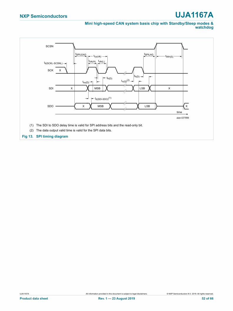
NXP Semiconductors UJA1167AMini high-speed CAN system basis chip with Standby/Sleep modes &
watchdog
(1) The SDI to SDO delay time is valid for SPI address bits and the read-only bit.
(2) The data output valid time is valid for the SPI data bits.
Fig 13. SPI timing diagram
aaa-027898
LSB XMSBX
X
SDI
SCK
SCSN
tSPILEAD tcy(clk)tSPILAG tWH(S)
th(D)th(D)tsu(D) tv(Q)(2)
tclk(H) tclk(L)
LSBMSB
time
XXSDO
td(SDI-SDO)(1)
td(SCKL-SCSNL)
UJA1167A All information provided in this document is subject to legal disclaimers. © NXP Semiconductors N.V. 2019. All rights reserved.
Product data sheet Rev. 1 — 23 August 2019 52 of 66

NXP Semiconductors UJA1167AMini high-speed CAN system basis chip with Standby/Sleep modes &
watchdog
12. Application information
12.1 Application diagram
(1) Actual capacitance value must be a least 1.76 F with 5 V DC offset (recommended capacitor value is 6.8 F).
(2) For bus line end nodes, RT = 60 in order to support the ‘split termination concept’. For sub-nodes, an optional ‘weak’ termination of e.g. RT = 1.3 k can be used, if required by the OEM.
Fig 14. Typical application using the UJA1167ATK/X
SDO
aaa-022894
RSTN
UJA1167ATK/X
3
GND
5RSTN
MICRO-CONTROLLER
6
8SCK
RXDRXD
4
TXDTXD1
SDI11
14SCSN
standardμC ports
VCC7
e.g. off-board sensor supply
V1VEXT
1213
2
BAT10
9
BAT
VSS
(1)
(1)
WAKE
10 nF
10 kΩ
CANH CANL
e.g.4.7 nF
RT (2)RT (2)
47 nF22 μF
UJA1167A All information provided in this document is subject to legal disclaimers. © NXP Semiconductors N.V. 2019. All rights reserved.
Product data sheet Rev. 1 — 23 August 2019 53 of 66
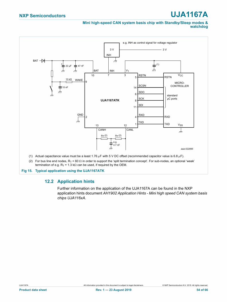
NXP Semiconductors UJA1167AMini high-speed CAN system basis chip with Standby/Sleep modes &
watchdog
12.2 Application hints
Further information on the application of the UJA1167A can be found in the NXP application hints document AH1902 Application Hints - Mini high speed CAN system basis chips UJA116xA.
(1) Actual capacitance value must be a least 1.76 F with 5 V DC offset (recommended capacitor value is 6.8 F).
(2) For bus line end nodes, RT = 60 in order to support the ‘split termination concept’. For sub-nodes, an optional ‘weak’ termination of e.g. RT = 1.3 k can be used, if required by the OEM.
Fig 15. Typical application using the UJA1167ATK
aaa-022895
UJA1167ATK
3
GND
5
6
8
4
1
11
14
7
e.g. INH as control signal for voltage regulator
INH
1213
2
INH
3 V 3 V
SDO
RSTNRSTN
MICRO-CONTROLLER
SCK
RXDRXD
TXDTXD
SDI
SCSN
standardμC ports
VCC
V1BAT
10
9
BAT
VSS
(1)
WAKE
10 nF
10 kΩ
CANH CANL
e.g.4.7 nF
RT (2)RT (2)
47 nF22 μF
UJA1167A All information provided in this document is subject to legal disclaimers. © NXP Semiconductors N.V. 2019. All rights reserved.
Product data sheet Rev. 1 — 23 August 2019 54 of 66
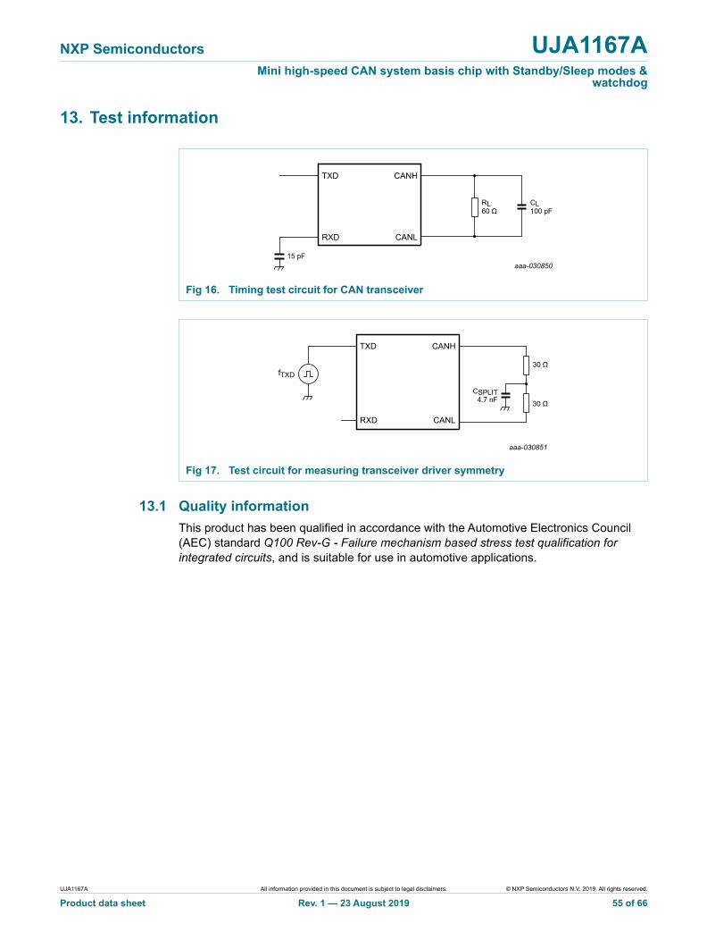
NXP Semiconductors UJA1167AMini high-speed CAN system basis chip with Standby/Sleep modes &
watchdog
13. Test information
13.1 Quality information
This product has been qualified in accordance with the Automotive Electronics Council (AEC) standard Q100 Rev-G - Failure mechanism based stress test qualification for integrated circuits, and is suitable for use in automotive applications.
Fig 16. Timing test circuit for CAN transceiver
Fig 17. Test circuit for measuring transceiver driver symmetry
aaa-030850
TXD
RXD
15 pF
CANL
CANH
RL60 Ω
CL100 pF
aaa-030851
30 Ω
30 Ω
CSPLIT4.7 nF
TXD
RXD CANL
CANH
fTXD
UJA1167A All information provided in this document is subject to legal disclaimers. © NXP Semiconductors N.V. 2019. All rights reserved.
Product data sheet Rev. 1 — 23 August 2019 55 of 66

NXP Semiconductors UJA1167AMini high-speed CAN system basis chip with Standby/Sleep modes &
watchdog
14. Package outline
Fig 18. Package outline SOT1086-2 (HVSON14)
ReferencesOutline version
European projection Issue date
IEC JEDEC JEITA
SOT1086-2 - - -MO-229- - -
sot1086-2
10-07-14 10-07-15
Unit
mmmax nom min
1.00 0.85 0.80
0.05 0.03 0.00
0.24.6 4.5 4.4
4.25 4.20 4.15
3.1 3.0 2.9
0.65 3.90.45 0.40 0.35
0.1
A
Dimensions
HVSON14: plastic, thermal enhanced very thin small outline package; no leads; 14 terminals; body 3 x 4.5 x 0.85 mm SOT1086-2
A1 b
0.35 0.32 0.29
c D Dh E Eh
1.65 1.60 1.55
e e1 k
0.35 0.30 0.25
L v
0.1
w
0.05
y
0.05
y1
0 2.5 5 mm
scale
B A
terminal 1 index area
D
E
X
detail X
A
cA1
C
yCy1
AC BvCwb
terminal 1 index area
e1
e
Dh
Eh
Lk
1
14
7
8
UJA1167A All information provided in this document is subject to legal disclaimers. © NXP Semiconductors N.V. 2019. All rights reserved.
Product data sheet Rev. 1 — 23 August 2019 56 of 66

NXP Semiconductors UJA1167AMini high-speed CAN system basis chip with Standby/Sleep modes &
watchdog
15. Handling information
All input and output pins are protected against ElectroStatic Discharge (ESD) under normal handling. When handling ensure that the appropriate precautions are taken as described in JESD625-A or equivalent standards.
16. Soldering of SMD packages
This text provides a very brief insight into a complex technology. A more in-depth account of soldering ICs can be found in Application Note AN10365 “Surface mount reflow soldering description”.
16.1 Introduction to soldering
Soldering is one of the most common methods through which packages are attached to Printed Circuit Boards (PCBs), to form electrical circuits. The soldered joint provides both the mechanical and the electrical connection. There is no single soldering method that is ideal for all IC packages. Wave soldering is often preferred when through-hole and Surface Mount Devices (SMDs) are mixed on one printed wiring board; however, it is not suitable for fine pitch SMDs. Reflow soldering is ideal for the small pitches and high densities that come with increased miniaturization.
16.2 Wave and reflow soldering
Wave soldering is a joining technology in which the joints are made by solder coming from a standing wave of liquid solder. The wave soldering process is suitable for the following:
• Through-hole components
• Leaded or leadless SMDs, which are glued to the surface of the printed circuit board
Not all SMDs can be wave soldered. Packages with solder balls, and some leadless packages which have solder lands underneath the body, cannot be wave soldered. Also, leaded SMDs with leads having a pitch smaller than ~0.6 mm cannot be wave soldered, due to an increased probability of bridging.
The reflow soldering process involves applying solder paste to a board, followed by component placement and exposure to a temperature profile. Leaded packages, packages with solder balls, and leadless packages are all reflow solderable.
Key characteristics in both wave and reflow soldering are:
• Board specifications, including the board finish, solder masks and vias
• Package footprints, including solder thieves and orientation
• The moisture sensitivity level of the packages
• Package placement
• Inspection and repair
• Lead-free soldering versus SnPb soldering
16.3 Wave soldering
Key characteristics in wave soldering are:
UJA1167A All information provided in this document is subject to legal disclaimers. © NXP Semiconductors N.V. 2019. All rights reserved.
Product data sheet Rev. 1 — 23 August 2019 57 of 66
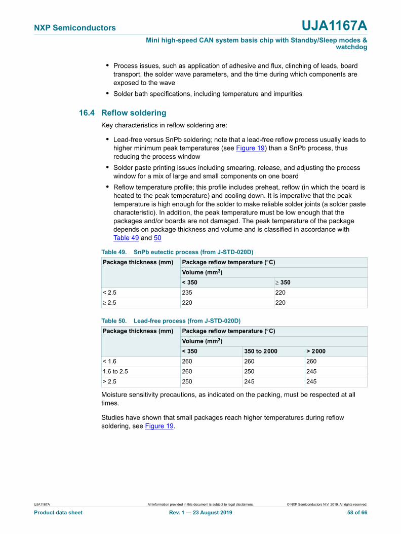
NXP Semiconductors UJA1167AMini high-speed CAN system basis chip with Standby/Sleep modes &
watchdog
• Process issues, such as application of adhesive and flux, clinching of leads, board transport, the solder wave parameters, and the time during which components are exposed to the wave
• Solder bath specifications, including temperature and impurities
16.4 Reflow soldering
Key characteristics in reflow soldering are:
• Lead-free versus SnPb soldering; note that a lead-free reflow process usually leads to higher minimum peak temperatures (see Figure 19) than a SnPb process, thus reducing the process window
• Solder paste printing issues including smearing, release, and adjusting the process window for a mix of large and small components on one board
• Reflow temperature profile; this profile includes preheat, reflow (in which the board is heated to the peak temperature) and cooling down. It is imperative that the peak temperature is high enough for the solder to make reliable solder joints (a solder paste characteristic). In addition, the peak temperature must be low enough that the packages and/or boards are not damaged. The peak temperature of the package depends on package thickness and volume and is classified in accordance with Table 49 and 50
Moisture sensitivity precautions, as indicated on the packing, must be respected at all times.
Studies have shown that small packages reach higher temperatures during reflow soldering, see Figure 19.
Table 49. SnPb eutectic process (from J-STD-020D)
Package thickness (mm) Package reflow temperature (C)
Volume (mm3)
< 350 350
< 2.5 235 220
2.5 220 220
Table 50. Lead-free process (from J-STD-020D)
Package thickness (mm) Package reflow temperature (C)
Volume (mm3)
< 350 350 to 2000 > 2000
< 1.6 260 260 260
1.6 to 2.5 260 250 245
> 2.5 250 245 245
UJA1167A All information provided in this document is subject to legal disclaimers. © NXP Semiconductors N.V. 2019. All rights reserved.
Product data sheet Rev. 1 — 23 August 2019 58 of 66
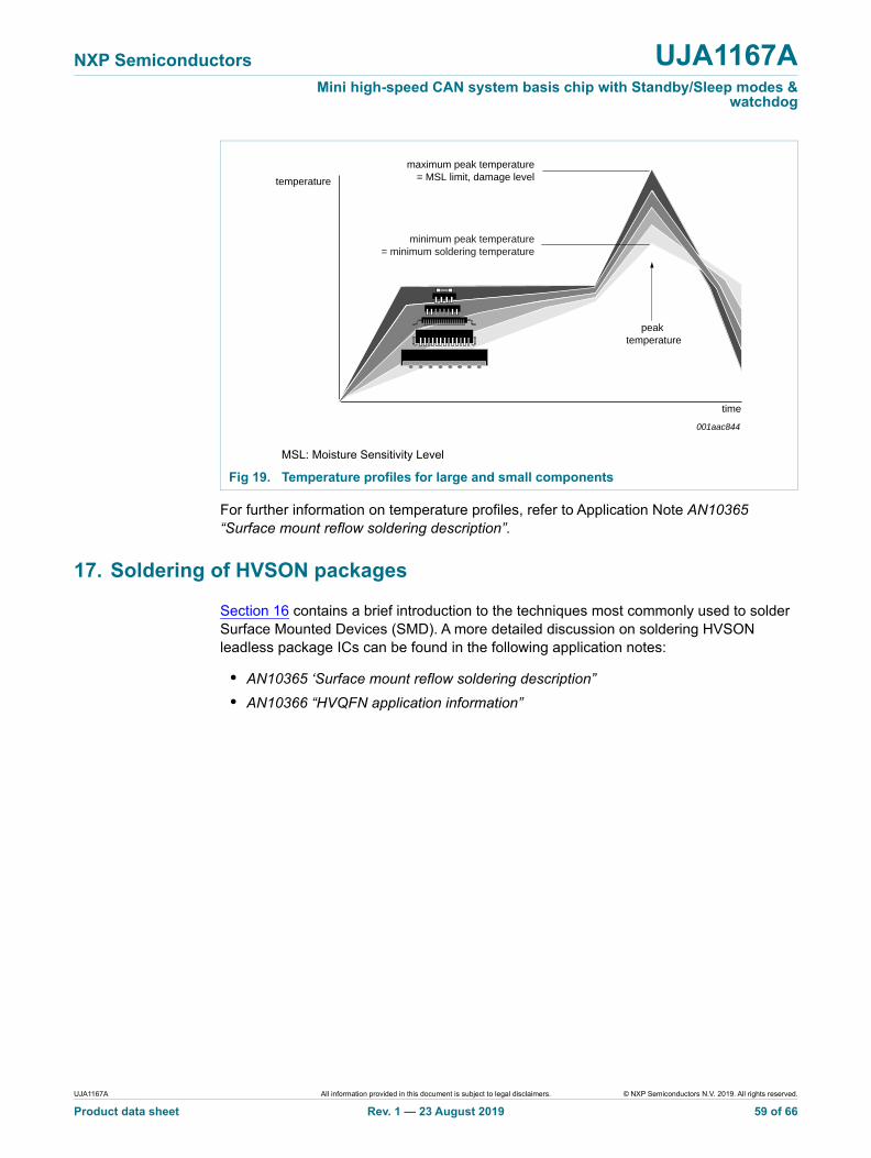
NXP Semiconductors UJA1167AMini high-speed CAN system basis chip with Standby/Sleep modes &
watchdog
For further information on temperature profiles, refer to Application Note AN10365 “Surface mount reflow soldering description”.
17. Soldering of HVSON packages
Section 16 contains a brief introduction to the techniques most commonly used to solder Surface Mounted Devices (SMD). A more detailed discussion on soldering HVSON leadless package ICs can be found in the following application notes:
• AN10365 ‘Surface mount reflow soldering description”
• AN10366 “HVQFN application information”
MSL: Moisture Sensitivity Level
Fig 19. Temperature profiles for large and small components
001aac844
temperature
time
minimum peak temperature= minimum soldering temperature
maximum peak temperature= MSL limit, damage level
peak temperature
UJA1167A All information provided in this document is subject to legal disclaimers. © NXP Semiconductors N.V. 2019. All rights reserved.
Product data sheet Rev. 1 — 23 August 2019 59 of 66

NXP Semiconductors UJA1167AMini high-speed CAN system basis chip with Standby/Sleep modes &
watchdog
18. Appendix: ISO 11898-2:201x parameter cross-reference list
Table 51. ISO 11898-2:201x to NXP data sheet parameter conversion
ISO 11898-2:201x NXP data sheet
Parameter Notation Symbol Parameter
HS-PMA dominant output characteristics
Single ended voltage on CAN_H VCAN_H VO(dom) dominant output voltage
Single ended voltage on CAN_L VCAN_L
Differential voltage on normal bus load VDiff VO(dif) differential output voltage
Differential voltage on effective resistance during arbitration
Optional: Differential voltage on extended bus load range
HS-PMA driver symmetry
Driver symmetry VSYM VTXsym transmitter voltage symmetry
Maximum HS-PMA driver output current
Absolute current on CAN_H ICAN_H IO(sc)dom dominant short-circuit output currentAbsolute current on CAN_L ICAN_L
HS-PMA recessive output characteristics, bus biasing active/inactive
Single ended output voltage on CAN_H VCAN_H VO(rec) recessive output voltage
Single ended output voltage on CAN_L VCAN_L
Differential output voltage VDiff VO(dif) differential output voltage
Optional HS-PMA transmit dominant timeout
Transmit dominant timeout, long tdom tto(dom)TXD TXD dominant time-out time
Transmit dominant timeout, short
HS-PMA static receiver input characteristics, bus biasing active/inactive
Recessive state differential input voltage range
Dominant state differential input voltage range
VDiff Vth(RX)dif differential receiver threshold voltage
Vrec(RX) receiver recessive voltage
Vdom(RX) receiver dominant voltage
HS-PMA receiver input resistance (matching)
Differential internal resistance RDiff Ri(dif) differential input resistance
Single ended internal resistance RCAN_HRCAN_L
Ri input resistance
Matching of internal resistance MR Ri input resistance deviation
HS-PMA implementation loop delay requirement
Loop delay tLoop td(TXDH-RXDH) delay time from TXD HIGH to RXD HIGH
td(TXDL-RXDL) delay time from TXD LOW to RXD LOW
Optional HS-PMA implementation data signal timing requirements for use with bit rates above 1 Mbit/s up to 2 Mbit/s and above 2 Mbit/s up to 5 Mbit/s
Transmitted recessive bit width @ 2 Mbit/s / @ 5 Mbit/s, intended
tBit(Bus) tbit(bus) transmitted recessive bit width
Received recessive bit width @ 2 Mbit/s / @ 5 Mbit/s tBit(RXD) tbit(RXD) bit time on pin RXD
Receiver timing symmetry @ 2 Mbit/s / @ 5 Mbit/s tRec trec receiver timing symmetry
UJA1167A All information provided in this document is subject to legal disclaimers. © NXP Semiconductors N.V. 2019. All rights reserved.
Product data sheet Rev. 1 — 23 August 2019 60 of 66
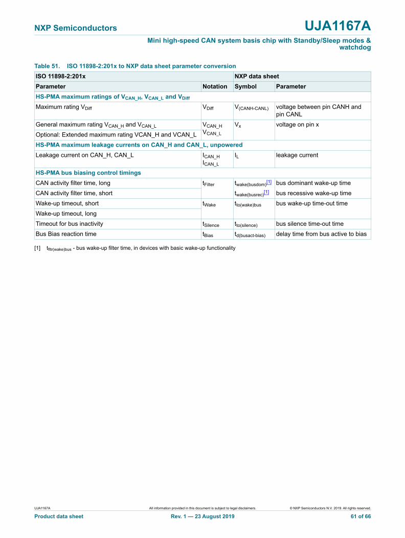
NXP Semiconductors UJA1167AMini high-speed CAN system basis chip with Standby/Sleep modes &
watchdog
[1] tfltr(wake)bus - bus wake-up filter time, in devices with basic wake-up functionality
HS-PMA maximum ratings of VCAN_H, VCAN_L and VDiff
Maximum rating VDiff VDiff V(CANH-CANL) voltage between pin CANH and pin CANL
General maximum rating VCAN_H and VCAN_L VCAN_H
VCAN_L
Vx voltage on pin x
Optional: Extended maximum rating VCAN_H and VCAN_L
HS-PMA maximum leakage currents on CAN_H and CAN_L, unpowered
Leakage current on CAN_H, CAN_L ICAN_H
ICAN_L
IL leakage current
HS-PMA bus biasing control timings
CAN activity filter time, long tFilter twake(busdom)[1] bus dominant wake-up time
CAN activity filter time, short twake(busrec)[1] bus recessive wake-up time
Wake-up timeout, short tWake tto(wake)bus bus wake-up time-out time
Wake-up timeout, long
Timeout for bus inactivity tSilence tto(silence) bus silence time-out time
Bus Bias reaction time tBias td(busact-bias) delay time from bus active to bias
Table 51. ISO 11898-2:201x to NXP data sheet parameter conversion
ISO 11898-2:201x NXP data sheet
Parameter Notation Symbol Parameter
UJA1167A All information provided in this document is subject to legal disclaimers. © NXP Semiconductors N.V. 2019. All rights reserved.
Product data sheet Rev. 1 — 23 August 2019 61 of 66

NXP Semiconductors UJA1167AMini high-speed CAN system basis chip with Standby/Sleep modes &
watchdog
19. Revision history
Table 52. Revision history
Document ID Release date Data sheet status Change notice Supersedes
UJA1167A v.1 20190823 Product data sheet - -
UJA1167A All information provided in this document is subject to legal disclaimers. © NXP Semiconductors N.V. 2019. All rights reserved.
Product data sheet Rev. 1 — 23 August 2019 62 of 66

NXP Semiconductors UJA1167AMini high-speed CAN system basis chip with Standby/Sleep modes &
watchdog
20. Legal information
20.1 Data sheet status
[1] Please consult the most recently issued document before initiating or completing a design.
[2] The term ‘short data sheet’ is explained in section “Definitions”.
[3] The product status of device(s) described in this document may have changed since this document was published and may differ in case of multiple devices. The latest product status information is available on the Internet at URL http://www.nxp.com.
20.2 Definitions
Draft — The document is a draft version only. The content is still under internal review and subject to formal approval, which may result in modifications or additions. NXP Semiconductors does not give any representations or warranties as to the accuracy or completeness of information included herein and shall have no liability for the consequences of use of such information.
Short data sheet — A short data sheet is an extract from a full data sheet with the same product type number(s) and title. A short data sheet is intended for quick reference only and should not be relied upon to contain detailed and full information. For detailed and full information see the relevant full data sheet, which is available on request via the local NXP Semiconductors sales office. In case of any inconsistency or conflict with the short data sheet, the full data sheet shall prevail.
Product specification — The information and data provided in a Product data sheet shall define the specification of the product as agreed between NXP Semiconductors and its customer, unless NXP Semiconductors and customer have explicitly agreed otherwise in writing. In no event however, shall an agreement be valid in which the NXP Semiconductors product is deemed to offer functions and qualities beyond those described in the Product data sheet.
20.3 Disclaimers
Limited warranty and liability — Information in this document is believed to be accurate and reliable. However, NXP Semiconductors does not give any representations or warranties, expressed or implied, as to the accuracy or completeness of such information and shall have no liability for the consequences of use of such information. NXP Semiconductors takes no responsibility for the content in this document if provided by an information source outside of NXP Semiconductors.
In no event shall NXP Semiconductors be liable for any indirect, incidental, punitive, special or consequential damages (including - without limitation - lost profits, lost savings, business interruption, costs related to the removal or replacement of any products or rework charges) whether or not such damages are based on tort (including negligence), warranty, breach of contract or any other legal theory.
Notwithstanding any damages that customer might incur for any reason whatsoever, NXP Semiconductors’ aggregate and cumulative liability towards customer for the products described herein shall be limited in accordance with the Terms and conditions of commercial sale of NXP Semiconductors.
Right to make changes — NXP Semiconductors reserves the right to make changes to information published in this document, including without limitation specifications and product descriptions, at any time and without notice. This document supersedes and replaces all information supplied prior to the publication hereof.
Suitability for use in automotive applications — This NXP Semiconductors product has been qualified for use in automotive applications. Unless otherwise agreed in writing, the product is not designed, authorized or warranted to be suitable for use in life support, life-critical or safety-critical systems or equipment, nor in applications where failure or malfunction of an NXP Semiconductors product can reasonably be expected to result in personal injury, death or severe property or environmental damage. NXP Semiconductors and its suppliers accept no liability for inclusion and/or use of NXP Semiconductors products in such equipment or applications and therefore such inclusion and/or use is at the customer's own risk.
Applications — Applications that are described herein for any of these products are for illustrative purposes only. NXP Semiconductors makes no representation or warranty that such applications will be suitable for the specified use without further testing or modification.
Customers are responsible for the design and operation of their applications and products using NXP Semiconductors products, and NXP Semiconductors accepts no liability for any assistance with applications or customer product design. It is customer’s sole responsibility to determine whether the NXP Semiconductors product is suitable and fit for the customer’s applications and products planned, as well as for the planned application and use of customer’s third party customer(s). Customers should provide appropriate design and operating safeguards to minimize the risks associated with their applications and products.
NXP Semiconductors does not accept any liability related to any default, damage, costs or problem which is based on any weakness or default in the customer’s applications or products, or the application or use by customer’s third party customer(s). Customer is responsible for doing all necessary testing for the customer’s applications and products using NXP Semiconductors products in order to avoid a default of the applications and the products or of the application or use by customer’s third party customer(s). NXP does not accept any liability in this respect.
Limiting values — Stress above one or more limiting values (as defined in the Absolute Maximum Ratings System of IEC 60134) will cause permanent damage to the device. Limiting values are stress ratings only and (proper) operation of the device at these or any other conditions above those given in the Recommended operating conditions section (if present) or the Characteristics sections of this document is not warranted. Constant or repeated exposure to limiting values will permanently and irreversibly affect the quality and reliability of the device.
Terms and conditions of commercial sale — NXP Semiconductors products are sold subject to the general terms and conditions of commercial sale, as published at http://www.nxp.com/profile/terms, unless otherwise agreed in a valid written individual agreement. In case an individual agreement is concluded only the terms and conditions of the respective agreement shall apply. NXP Semiconductors hereby expressly objects to applying the customer’s general terms and conditions with regard to the purchase of NXP Semiconductors products by customer.
Document status[1][2] Product status[3] Definition
Objective [short] data sheet Development This document contains data from the objective specification for product development.
Preliminary [short] data sheet Qualification This document contains data from the preliminary specification.
Product [short] data sheet Production This document contains the product specification.
UJA1167A All information provided in this document is subject to legal disclaimers. © NXP Semiconductors N.V. 2019. All rights reserved.
Product data sheet Rev. 1 — 23 August 2019 63 of 66
NXP Semiconductors UJA1167AMini high-speed CAN system basis chip with Standby/Sleep modes &
watchdog
No offer to sell or license — Nothing in this document may be interpreted or construed as an offer to sell products that is open for acceptance or the grant, conveyance or implication of any license under any copyrights, patents or other industrial or intellectual property rights.
Export control — This document as well as the item(s) described herein may be subject to export control regulations. Export might require a prior authorization from competent authorities.
Translations — A non-English (translated) version of a document is for reference only. The English version shall prevail in case of any discrepancy between the translated and English versions.
20.4 TrademarksNotice: All referenced brands, product names, service names and trademarks are the property of their respective owners.
21. Contact information
For more information, please visit: http://www.nxp.com
For sales office addresses, please send an email to: [email protected]
UJA1167A All information provided in this document is subject to legal disclaimers. © NXP Semiconductors N.V. 2019. All rights reserved.
Product data sheet Rev. 1 — 23 August 2019 64 of 66

NXP Semiconductors UJA1167AMini high-speed CAN system basis chip with Standby/Sleep modes &
watchdog
22. Contents
1 General description . . . . . . . . . . . . . . . . . . . . . . 1
2 Features and benefits . . . . . . . . . . . . . . . . . . . . 12.1 General . . . . . . . . . . . . . . . . . . . . . . . . . . . . . . . 12.2 Designed for automotive applications. . . . . . . . 12.3 Low-drop voltage regulator for 5 V microcontroller
supply (V1) . . . . . . . . . . . . . . . . . . . . . . . . . . . . 22.4 Power Management . . . . . . . . . . . . . . . . . . . . . 22.5 System control and diagnostic features . . . . . . 22.6 Sensor supply voltage (pin VEXT of
UJA1167ATK/X) . . . . . . . . . . . . . . . . . . . . . . . . 3
3 Product family overview . . . . . . . . . . . . . . . . . . 4
4 Ordering information. . . . . . . . . . . . . . . . . . . . . 4
5 Block diagram . . . . . . . . . . . . . . . . . . . . . . . . . . 5
6 Pinning information. . . . . . . . . . . . . . . . . . . . . . 66.1 Pinning . . . . . . . . . . . . . . . . . . . . . . . . . . . . . . . 66.2 Pin description . . . . . . . . . . . . . . . . . . . . . . . . . 6
7 Functional description . . . . . . . . . . . . . . . . . . . 77.1 System controller . . . . . . . . . . . . . . . . . . . . . . . 77.1.1 Operating modes . . . . . . . . . . . . . . . . . . . . . . . 77.1.1.1 Normal mode . . . . . . . . . . . . . . . . . . . . . . . . . . 77.1.1.2 Standby mode . . . . . . . . . . . . . . . . . . . . . . . . . 77.1.1.3 Sleep mode . . . . . . . . . . . . . . . . . . . . . . . . . . . 87.1.1.4 Reset mode . . . . . . . . . . . . . . . . . . . . . . . . . . . 97.1.1.5 Off mode. . . . . . . . . . . . . . . . . . . . . . . . . . . . . . 97.1.1.6 Overtemp mode . . . . . . . . . . . . . . . . . . . . . . . 107.1.1.7 Forced Normal mode . . . . . . . . . . . . . . . . . . . 107.1.1.8 Hardware characterization for the UJA1167A
operating modes. . . . . . . . . . . . . . . . . . . . . . . 117.1.2 System control registers . . . . . . . . . . . . . . . . . 117.2 Watchdog . . . . . . . . . . . . . . . . . . . . . . . . . . . . 127.2.1 Software Development mode . . . . . . . . . . . . . 157.2.2 Watchdog behavior in Window mode . . . . . . . 157.2.3 Watchdog behavior in Timeout mode . . . . . . . 157.2.4 Watchdog behavior in Autonomous mode . . . 167.3 System reset. . . . . . . . . . . . . . . . . . . . . . . . . . 167.3.1 Characteristics of pin RSTN . . . . . . . . . . . . . . 167.3.2 Selecting the output reset pulse width . . . . . . 177.3.3 Reset sources. . . . . . . . . . . . . . . . . . . . . . . . . 177.4 Global temperature protection . . . . . . . . . . . . 187.5 Power supplies . . . . . . . . . . . . . . . . . . . . . . . . 187.5.1 Battery supply voltage (VBAT) . . . . . . . . . . . . . 187.5.2 Low-drop voltage supply for 5 V microcontroller
(V1) . . . . . . . . . . . . . . . . . . . . . . . . . . . . . . . . . 187.6 High voltage output and external sensor supply. .
197.7 High-speed CAN transceiver . . . . . . . . . . . . . 207.7.1 CAN operating modes . . . . . . . . . . . . . . . . . . 20
7.7.1.1 CAN Active mode. . . . . . . . . . . . . . . . . . . . . . 207.7.1.2 CAN Listen-only mode . . . . . . . . . . . . . . . . . . 217.7.1.3 CAN Offline and Offline Bias modes . . . . . . . 217.7.1.4 CAN Off mode . . . . . . . . . . . . . . . . . . . . . . . . 227.7.2 CAN standard wake-up . . . . . . . . . . . . . . . . . 237.7.3 CAN control and Transceiver status registers 247.8 CAN fail-safe features . . . . . . . . . . . . . . . . . . 257.8.1 TXD dominant timeout . . . . . . . . . . . . . . . . . . 257.8.2 Pull-up on TXD pin. . . . . . . . . . . . . . . . . . . . . 257.8.3 V1 undervoltage event . . . . . . . . . . . . . . . . . . 257.8.4 Loss of power at pin BAT . . . . . . . . . . . . . . . . 257.9 Local wake-up via WAKE pin . . . . . . . . . . . . . 257.10 Wake-up and interrupt event diagnosis via pin
RXD . . . . . . . . . . . . . . . . . . . . . . . . . . . . . . . . 267.10.1 Interrupt/wake-up delay . . . . . . . . . . . . . . . . . 277.10.2 Sleep mode protection . . . . . . . . . . . . . . . . . . 277.10.3 Event status and event capture registers. . . . 287.11 Non-volatile SBC configuration . . . . . . . . . . . 317.11.1 Programming MTPNV cells . . . . . . . . . . . . . . 317.11.1.1 Calculating the CRC value for MTP programming
327.11.2 Restoring factory preset values . . . . . . . . . . . 337.12 Device ID . . . . . . . . . . . . . . . . . . . . . . . . . . . . 337.13 Lock control register. . . . . . . . . . . . . . . . . . . . 337.14 General purpose memory . . . . . . . . . . . . . . . 347.15 SPI . . . . . . . . . . . . . . . . . . . . . . . . . . . . . . . . . 347.15.1 Introduction . . . . . . . . . . . . . . . . . . . . . . . . . . 347.15.2 Register map . . . . . . . . . . . . . . . . . . . . . . . . . 377.15.3 Register configuration in UJA1167A operating
modes . . . . . . . . . . . . . . . . . . . . . . . . . . . . . . 38
8 Limiting values . . . . . . . . . . . . . . . . . . . . . . . . 41
9 Thermal characteristics . . . . . . . . . . . . . . . . . 43
10 Static characteristics . . . . . . . . . . . . . . . . . . . 43
11 Dynamic characteristics. . . . . . . . . . . . . . . . . 48
12 Application information . . . . . . . . . . . . . . . . . 5312.1 Application diagram . . . . . . . . . . . . . . . . . . . . 5312.2 Application hints. . . . . . . . . . . . . . . . . . . . . . . 54
13 Test information . . . . . . . . . . . . . . . . . . . . . . . 5513.1 Quality information . . . . . . . . . . . . . . . . . . . . . 55
14 Package outline. . . . . . . . . . . . . . . . . . . . . . . . 56
15 Handling information . . . . . . . . . . . . . . . . . . . 57
16 Soldering of SMD packages. . . . . . . . . . . . . . 5716.1 Introduction to soldering. . . . . . . . . . . . . . . . . 5716.2 Wave and reflow soldering. . . . . . . . . . . . . . . 5716.3 Wave soldering . . . . . . . . . . . . . . . . . . . . . . . 5716.4 Reflow soldering . . . . . . . . . . . . . . . . . . . . . . 58
UJA1167A All information provided in this document is subject to legal disclaimers. © NXP Semiconductors N.V. 2019. All rights reserved.
Product data sheet Rev. 1 — 23 August 2019 65 of 66
continued >>

NXP Semiconductors UJA1167AMini high-speed CAN system basis chip with Standby/Sleep modes &
watchdog
17 Soldering of HVSON packages. . . . . . . . . . . . 59
18 Appendix: ISO 11898-2:201x parameter cross-reference list . . . . . . . . . . . . . . . . . . . . . 60
19 Revision history. . . . . . . . . . . . . . . . . . . . . . . . 62
20 Legal information. . . . . . . . . . . . . . . . . . . . . . . 6320.1 Data sheet status . . . . . . . . . . . . . . . . . . . . . . 6320.2 Definitions. . . . . . . . . . . . . . . . . . . . . . . . . . . . 6320.3 Disclaimers . . . . . . . . . . . . . . . . . . . . . . . . . . . 6320.4 Trademarks. . . . . . . . . . . . . . . . . . . . . . . . . . . 64
21 Contact information. . . . . . . . . . . . . . . . . . . . . 64
22 Contents . . . . . . . . . . . . . . . . . . . . . . . . . . . . . . 65
© NXP Semiconductors N.V. 2019. All rights reserved.
For more information, please visit: http://www.nxp.comFor sales office addresses, please send an email to: [email protected]
Date of release: 23 August 2019
Document identifier: UJA1167A
Please be aware that important notices concerning this document and the product(s)described herein, have been included in section ‘Legal information’.