Embed Size (px)
Citation preview
UG0449User Guide
SmartFusion2 and IGLOO2 Clocking Resources

50200449. 9.0 9/21
Microsemi HeadquartersOne Enterprise, Aliso Viejo,CA 92656 USAWithin the USA: +1 (800) 713-4113 Outside the USA: +1 (949) 380-6100Sales: +1 (949) 380-6136Fax: +1 (949) 215-4996Email: [email protected]
©2021 Microsemi, a wholly owned subsidiary of Microchip Technology Inc. All rights reserved. Microsemi and the Microsemi logo are registered trademarks of Microsemi Corporation. All other trademarks and service marks are the property of their respective owners.
Microsemi makes no warranty, representation, or guarantee regarding the information contained herein or the suitability of its products and services for any particular purpose, nor does Microsemi assume any liability whatsoever arising out of the application or use of any product or circuit. The products sold hereunder and any other products sold by Microsemi have been subject to limited testing and should not be used in conjunction with mission-critical equipment or applications. Any performance specifications are believed to be reliable but are not verified, and Buyer must conduct and complete all performance and other testing of the products, alone and together with, or installed in, any end-products. Buyer shall not rely on any data and performance specifications or parameters provided by Microsemi. It is the Buyer’s responsibility to independently determine suitability of any products and to test and verify the same. The information provided by Microsemi hereunder is provided “as is, where is” and with all faults, and the entire risk associated with such information is entirely with the Buyer. Microsemi does not grant, explicitly or implicitly, to any party any patent rights, licenses, or any other IP rights, whether with regard to such information itself or anything described by such information. Information provided in this document is proprietary to Microsemi, and Microsemi reserves the right to make any changes to the information in this document or to any products and services at any time without notice.
About MicrosemiMicrosemi, a wholly owned subsidiary of Microchip Technology Inc. (Nasdaq: MCHP), offers a comprehensive portfolio of semiconductor and system solutions for aerospace & defense, communications, data center and industrial markets. Products include high-performance and radiation-hardened analog mixed-signal integrated circuits, FPGAs, SoCs and ASICs; power management products; timing and synchronization devices and precise time solutions, setting the world's standard for time; voice processing devices; RF solutions; discrete components; enterprise storage and communication solutions, security technologies and scalable anti-tamper products; Ethernet solutions; Power-over-Ethernet ICs and midspans; as well as custom design capabilities and services. Learn more at www.microsemi.com.
Microsemi Proprietary UG0449 User Guide Revision 9.0 iii
Contents
1 Revision History . . . . . . . . . . . . . . . . . . . . . . . . . . . . . . . . . . . . . . . . . . . . . . . . . . . . . 11.1 Revision 9.0 . . . . . . . . . . . . . . . . . . . . . . . . . . . . . . . . . . . . . . . . . . . . . . . . . . . . . . . . . . . . . . . . . . . . . . . 11.2 Revision 8.0 . . . . . . . . . . . . . . . . . . . . . . . . . . . . . . . . . . . . . . . . . . . . . . . . . . . . . . . . . . . . . . . . . . . . . . . 11.3 Revision 7.0 . . . . . . . . . . . . . . . . . . . . . . . . . . . . . . . . . . . . . . . . . . . . . . . . . . . . . . . . . . . . . . . . . . . . . . . 11.4 Revision 6.0 . . . . . . . . . . . . . . . . . . . . . . . . . . . . . . . . . . . . . . . . . . . . . . . . . . . . . . . . . . . . . . . . . . . . . . . 11.5 Revision 5.0 . . . . . . . . . . . . . . . . . . . . . . . . . . . . . . . . . . . . . . . . . . . . . . . . . . . . . . . . . . . . . . . . . . . . . . . 11.6 Revision 4.0 . . . . . . . . . . . . . . . . . . . . . . . . . . . . . . . . . . . . . . . . . . . . . . . . . . . . . . . . . . . . . . . . . . . . . . . 11.7 Revision 3.0 . . . . . . . . . . . . . . . . . . . . . . . . . . . . . . . . . . . . . . . . . . . . . . . . . . . . . . . . . . . . . . . . . . . . . . . 21.8 Revision 2.0 . . . . . . . . . . . . . . . . . . . . . . . . . . . . . . . . . . . . . . . . . . . . . . . . . . . . . . . . . . . . . . . . . . . . . . . 31.9 Revision 1.0 . . . . . . . . . . . . . . . . . . . . . . . . . . . . . . . . . . . . . . . . . . . . . . . . . . . . . . . . . . . . . . . . . . . . . . . 3
2 Clocking Resources Overview . . . . . . . . . . . . . . . . . . . . . . . . . . . . . . . . . . . . . . . . . . 42.1 Clocking Scheme Overview . . . . . . . . . . . . . . . . . . . . . . . . . . . . . . . . . . . . . . . . . . . . . . . . . . . . . . . . . . . 5
3 FPGA Fabric Global Network Architecture . . . . . . . . . . . . . . . . . . . . . . . . . . . . . . . . 83.1 Global Network Architecture . . . . . . . . . . . . . . . . . . . . . . . . . . . . . . . . . . . . . . . . . . . . . . . . . . . . . . . . . . 8
3.1.1 Dedicated Global I/Os . . . . . . . . . . . . . . . . . . . . . . . . . . . . . . . . . . . . . . . . . . . . . . . . . . . . . . . 123.1.2 Fabric CCC . . . . . . . . . . . . . . . . . . . . . . . . . . . . . . . . . . . . . . . . . . . . . . . . . . . . . . . . . . . . . . . 163.1.3 VCCC . . . . . . . . . . . . . . . . . . . . . . . . . . . . . . . . . . . . . . . . . . . . . . . . . . . . . . . . . . . . . . . . . . . 163.1.4 Global Buffer . . . . . . . . . . . . . . . . . . . . . . . . . . . . . . . . . . . . . . . . . . . . . . . . . . . . . . . . . . . . . . 163.1.5 Row Global Buffers . . . . . . . . . . . . . . . . . . . . . . . . . . . . . . . . . . . . . . . . . . . . . . . . . . . . . . . . . 203.1.6 Clock Gating . . . . . . . . . . . . . . . . . . . . . . . . . . . . . . . . . . . . . . . . . . . . . . . . . . . . . . . . . . . . . . 20
3.2 Design Recommendations . . . . . . . . . . . . . . . . . . . . . . . . . . . . . . . . . . . . . . . . . . . . . . . . . . . . . . . . . . . 223.2.1 Global Macros . . . . . . . . . . . . . . . . . . . . . . . . . . . . . . . . . . . . . . . . . . . . . . . . . . . . . . . . . . . . . 223.2.2 Managing Global Signals . . . . . . . . . . . . . . . . . . . . . . . . . . . . . . . . . . . . . . . . . . . . . . . . . . . . . 233.2.3 Place and Route . . . . . . . . . . . . . . . . . . . . . . . . . . . . . . . . . . . . . . . . . . . . . . . . . . . . . . . . . . . 25
4 On-Chip Oscillators . . . . . . . . . . . . . . . . . . . . . . . . . . . . . . . . . . . . . . . . . . . . . . . . . 284.1 Functional Description . . . . . . . . . . . . . . . . . . . . . . . . . . . . . . . . . . . . . . . . . . . . . . . . . . . . . . . . . . . . . . 29
4.1.1 1 MHz RC Oscillator . . . . . . . . . . . . . . . . . . . . . . . . . . . . . . . . . . . . . . . . . . . . . . . . . . . . . . . . 294.1.2 50 MHz RC Oscillator . . . . . . . . . . . . . . . . . . . . . . . . . . . . . . . . . . . . . . . . . . . . . . . . . . . . . . . 304.1.3 Main Crystal Oscillator . . . . . . . . . . . . . . . . . . . . . . . . . . . . . . . . . . . . . . . . . . . . . . . . . . . . . . . 314.1.4 Auxiliary Crystal Oscillator . . . . . . . . . . . . . . . . . . . . . . . . . . . . . . . . . . . . . . . . . . . . . . . . . . . . 34
4.2 How to Use On-Chip Oscillators . . . . . . . . . . . . . . . . . . . . . . . . . . . . . . . . . . . . . . . . . . . . . . . . . . . . . . 354.2.1 Simulation Support . . . . . . . . . . . . . . . . . . . . . . . . . . . . . . . . . . . . . . . . . . . . . . . . . . . . . . . . . 374.2.2 On-Chip Oscillator Driving Fabric CCC(s) . . . . . . . . . . . . . . . . . . . . . . . . . . . . . . . . . . . . . . . . 374.2.3 On-Chip Oscillator Driving User Logic . . . . . . . . . . . . . . . . . . . . . . . . . . . . . . . . . . . . . . . . . . . 384.2.4 MSS RTC Clock Source Selection . . . . . . . . . . . . . . . . . . . . . . . . . . . . . . . . . . . . . . . . . . . . . 38
5 Fabric Clock Conditioning Circuitry . . . . . . . . . . . . . . . . . . . . . . . . . . . . . . . . . . . . . 395.1 Features . . . . . . . . . . . . . . . . . . . . . . . . . . . . . . . . . . . . . . . . . . . . . . . . . . . . . . . . . . . . . . . . . . . . . . . . . 395.2 System-Level Block Diagram . . . . . . . . . . . . . . . . . . . . . . . . . . . . . . . . . . . . . . . . . . . . . . . . . . . . . . . . . 405.3 Fabric CCC Locations . . . . . . . . . . . . . . . . . . . . . . . . . . . . . . . . . . . . . . . . . . . . . . . . . . . . . . . . . . . . . . 415.4 Functional Description . . . . . . . . . . . . . . . . . . . . . . . . . . . . . . . . . . . . . . . . . . . . . . . . . . . . . . . . . . . . . . 44
5.4.1 Fabric CCC Output Clocks . . . . . . . . . . . . . . . . . . . . . . . . . . . . . . . . . . . . . . . . . . . . . . . . . . . 475.4.2 Fabric CCC Clock Sources . . . . . . . . . . . . . . . . . . . . . . . . . . . . . . . . . . . . . . . . . . . . . . . . . . . 475.4.3 Fabric PLL Circuitry . . . . . . . . . . . . . . . . . . . . . . . . . . . . . . . . . . . . . . . . . . . . . . . . . . . . . . . . . 495.4.4 GPMUX . . . . . . . . . . . . . . . . . . . . . . . . . . . . . . . . . . . . . . . . . . . . . . . . . . . . . . . . . . . . . . . . . . 525.4.5 GPD . . . . . . . . . . . . . . . . . . . . . . . . . . . . . . . . . . . . . . . . . . . . . . . . . . . . . . . . . . . . . . . . . . . . . 535.4.6 NGMUX . . . . . . . . . . . . . . . . . . . . . . . . . . . . . . . . . . . . . . . . . . . . . . . . . . . . . . . . . . . . . . . . . . 56

Microsemi Proprietary UG0449 User Guide Revision 9.0 iv
5.4.7 Clock Gating . . . . . . . . . . . . . . . . . . . . . . . . . . . . . . . . . . . . . . . . . . . . . . . . . . . . . . . . . . . . . . 585.5 Fabric CCC Configuration . . . . . . . . . . . . . . . . . . . . . . . . . . . . . . . . . . . . . . . . . . . . . . . . . . . . . . . . . . . 58
5.5.1 Fabric CCC Static Configuration . . . . . . . . . . . . . . . . . . . . . . . . . . . . . . . . . . . . . . . . . . . . . . . 585.5.2 Fabric CCC Dynamic Configuration . . . . . . . . . . . . . . . . . . . . . . . . . . . . . . . . . . . . . . . . . . . . 58
5.6 Fabric CCC Configuration Registers . . . . . . . . . . . . . . . . . . . . . . . . . . . . . . . . . . . . . . . . . . . . . . . . . . . 595.6.1 Fabric CCC Configuration Registers Bit Definitions . . . . . . . . . . . . . . . . . . . . . . . . . . . . . . . . 60
5.7 How to Use Fabric CCC(s) . . . . . . . . . . . . . . . . . . . . . . . . . . . . . . . . . . . . . . . . . . . . . . . . . . . . . . . . . . . 705.7.1 Basic Configuration . . . . . . . . . . . . . . . . . . . . . . . . . . . . . . . . . . . . . . . . . . . . . . . . . . . . . . . . . 715.7.2 Advanced Configuration . . . . . . . . . . . . . . . . . . . . . . . . . . . . . . . . . . . . . . . . . . . . . . . . . . . . . 735.7.3 PLL Options . . . . . . . . . . . . . . . . . . . . . . . . . . . . . . . . . . . . . . . . . . . . . . . . . . . . . . . . . . . . . . . 815.7.4 Simulation Support . . . . . . . . . . . . . . . . . . . . . . . . . . . . . . . . . . . . . . . . . . . . . . . . . . . . . . . . . 835.7.5 Clock Frequency Synthesis . . . . . . . . . . . . . . . . . . . . . . . . . . . . . . . . . . . . . . . . . . . . . . . . . . . 835.7.6 Clock Delay Adjustment . . . . . . . . . . . . . . . . . . . . . . . . . . . . . . . . . . . . . . . . . . . . . . . . . . . . . 855.7.7 External Clock Source Through Dedicated Global I/O . . . . . . . . . . . . . . . . . . . . . . . . . . . . . . 85
6 MSS/HPMS Clock Conditioning Circuitry . . . . . . . . . . . . . . . . . . . . . . . . . . . . . . . . 876.1 Features . . . . . . . . . . . . . . . . . . . . . . . . . . . . . . . . . . . . . . . . . . . . . . . . . . . . . . . . . . . . . . . . . . . . . . . . . 876.2 Functional Description . . . . . . . . . . . . . . . . . . . . . . . . . . . . . . . . . . . . . . . . . . . . . . . . . . . . . . . . . . . . . . 88
6.2.1 MPLL . . . . . . . . . . . . . . . . . . . . . . . . . . . . . . . . . . . . . . . . . . . . . . . . . . . . . . . . . . . . . . . . . . . . 906.2.2 FACC . . . . . . . . . . . . . . . . . . . . . . . . . . . . . . . . . . . . . . . . . . . . . . . . . . . . . . . . . . . . . . . . . . . . 916.2.3 MSS CCC or HPMS CCC Operational Modes . . . . . . . . . . . . . . . . . . . . . . . . . . . . . . . . . . . . 956.2.4 PLLs Lock Monitoring . . . . . . . . . . . . . . . . . . . . . . . . . . . . . . . . . . . . . . . . . . . . . . . . . . . . . . . 96
6.3 Startup Clock Configuration Sequence . . . . . . . . . . . . . . . . . . . . . . . . . . . . . . . . . . . . . . . . . . . . . . . . . 976.4 MSS CCC or HPMS CCC Configuration . . . . . . . . . . . . . . . . . . . . . . . . . . . . . . . . . . . . . . . . . . . . . . . . 976.5 How to Use MSS CCC . . . . . . . . . . . . . . . . . . . . . . . . . . . . . . . . . . . . . . . . . . . . . . . . . . . . . . . . . . . . . . 98
6.5.1 Configuring Clocks . . . . . . . . . . . . . . . . . . . . . . . . . . . . . . . . . . . . . . . . . . . . . . . . . . . . . . . . . 996.5.2 How to Clock MSS and FIC Subsystems for Synchronous communication . . . . . . . . . . . . . 101
6.6 How to Use HPMS Clocks . . . . . . . . . . . . . . . . . . . . . . . . . . . . . . . . . . . . . . . . . . . . . . . . . . . . . . . . . . 1026.6.1 Configuring Clocks . . . . . . . . . . . . . . . . . . . . . . . . . . . . . . . . . . . . . . . . . . . . . . . . . . . . . . . . 1036.6.2 Clocking HPMS and FIC Subsystems . . . . . . . . . . . . . . . . . . . . . . . . . . . . . . . . . . . . . . . . . . 105
6.7 SYSREG Control Registers . . . . . . . . . . . . . . . . . . . . . . . . . . . . . . . . . . . . . . . . . . . . . . . . . . . . . . . . . 107
Microsemi Proprietary UG0449 User Guide Revision 9.0 v
Figures
Figure 1 SmartFusion2 SoC FPGA Device Clocking Scheme . . . . . . . . . . . . . . . . . . . . . . . . . . . . . . . . . . . . 5Figure 2 IGLOO2 FPGA Device Clocking Scheme . . . . . . . . . . . . . . . . . . . . . . . . . . . . . . . . . . . . . . . . . . . . . 6Figure 3 Global Signal Routing . . . . . . . . . . . . . . . . . . . . . . . . . . . . . . . . . . . . . . . . . . . . . . . . . . . . . . . . . . . . 9Figure 4 Global Network Architecture for SmartFusion2 and IGLOO2 M2S150/M2GL150 Devices . . . . . . 10Figure 5 Global Network Architecture for SmartFusion2 and IGLOO2 M2S025/M2GL025, M2S050/M2GL050,
M2S060/M2GL060, and M2S090/M2GL090 Devices . . . . . . . . . . . . . . . . . . . . . . . . . . . . . . . . . . . 11Figure 6 Global Network Architecture for SmartFusion2 and IGLOO2 M2S005/M2GL005 and
M2S010/M2GL010 Devices . . . . . . . . . . . . . . . . . . . . . . . . . . . . . . . . . . . . . . . . . . . . . . . . . . . . . . 12Figure 7 Dedicated Global I/Os (South-West Quadrant) Assignment in M2S025/M2GL025,
M2S050/M2GL050, M2S060/M2GL060, M2S090/M2GL090, and M2S150/M2GL150 Devices . . 14Figure 8 Dedicated Global I/Os (North-East Quadrant) Assignment in M2S005/M2GL005, and
M2S010/M2GL010 Devices . . . . . . . . . . . . . . . . . . . . . . . . . . . . . . . . . . . . . . . . . . . . . . . . . . . . . . 15Figure 9 VCCC Functional Block Diagram . . . . . . . . . . . . . . . . . . . . . . . . . . . . . . . . . . . . . . . . . . . . . . . . . . 16Figure 10 Various Sources Feeding Global Buffers for 2VS16 Global Network Architecture . . . . . . . . . . . . . 17Figure 11 Various Sources Feeding Global Buffers for 1VS8 Global Network Architecture . . . . . . . . . . . . . . 17Figure 12 Row Global Signals Driving Clusters . . . . . . . . . . . . . . . . . . . . . . . . . . . . . . . . . . . . . . . . . . . . . . . 20Figure 13 Clock Gating Circuit Schematic . . . . . . . . . . . . . . . . . . . . . . . . . . . . . . . . . . . . . . . . . . . . . . . . . . . 21Figure 14 Timing Waveforms for the Clock Gating Circuitry . . . . . . . . . . . . . . . . . . . . . . . . . . . . . . . . . . . . . . 21Figure 15 Synthesize Options Dialog Box . . . . . . . . . . . . . . . . . . . . . . . . . . . . . . . . . . . . . . . . . . . . . . . . . . . 24Figure 16 Example of Global Net Report 1 . . . . . . . . . . . . . . . . . . . . . . . . . . . . . . . . . . . . . . . . . . . . . . . . . . . 26Figure 17 Example of Global Net Report 2 . . . . . . . . . . . . . . . . . . . . . . . . . . . . . . . . . . . . . . . . . . . . . . . . . . . 26Figure 18 Example of Global Net Report 3 . . . . . . . . . . . . . . . . . . . . . . . . . . . . . . . . . . . . . . . . . . . . . . . . . . . 27Figure 19 SmartFusion2 On-Chip Oscillators Clock Sourcing Capabilities . . . . . . . . . . . . . . . . . . . . . . . . . . . 28Figure 20 IGLOO2 On-Chip Oscillators Clock Sourcing Capabilities . . . . . . . . . . . . . . . . . . . . . . . . . . . . . . . 29Figure 21 1 MHz RC Oscillator Clock Sourcing Capabilities . . . . . . . . . . . . . . . . . . . . . . . . . . . . . . . . . . . . . . 30Figure 22 50 MHz RC Oscillator Clock Sourcing Capabilities . . . . . . . . . . . . . . . . . . . . . . . . . . . . . . . . . . . . . 31Figure 23 Main Crystal Oscillator Clock Sourcing Capabilities . . . . . . . . . . . . . . . . . . . . . . . . . . . . . . . . . . . . 32Figure 24 Main Crystal Oscillator in RC Network Mode . . . . . . . . . . . . . . . . . . . . . . . . . . . . . . . . . . . . . . . . . 33Figure 25 Main Crystal Oscillator in Ceramic Resonator or Crystal Mode . . . . . . . . . . . . . . . . . . . . . . . . . . . 34Figure 26 Auxiliary Crystal Oscillator Clock Sourcing Capabilities in SmartFusion2 Devices . . . . . . . . . . . . 35Figure 27 Chip Oscillators Macro Configurator . . . . . . . . . . . . . . . . . . . . . . . . . . . . . . . . . . . . . . . . . . . . . . . . 35Figure 28 Select the Oscillator(s) . . . . . . . . . . . . . . . . . . . . . . . . . . . . . . . . . . . . . . . . . . . . . . . . . . . . . . . . . . 36Figure 29 Select the On-chip Oscillator(s) Resource Type . . . . . . . . . . . . . . . . . . . . . . . . . . . . . . . . . . . . . . . 36Figure 30 Main Crystal Oscillator and Fabric CCC Connectivity . . . . . . . . . . . . . . . . . . . . . . . . . . . . . . . . . . . 36Figure 31 Chip Oscillators Simulation Results . . . . . . . . . . . . . . . . . . . . . . . . . . . . . . . . . . . . . . . . . . . . . . . . 37Figure 32 Fabric CCC Reference Clock Selection . . . . . . . . . . . . . . . . . . . . . . . . . . . . . . . . . . . . . . . . . . . . . 37Figure 33 Main Crystal Oscillator Driving Fabric CCC . . . . . . . . . . . . . . . . . . . . . . . . . . . . . . . . . . . . . . . . . . 38Figure 34 50 MHz RC Oscillator Driving User Logic . . . . . . . . . . . . . . . . . . . . . . . . . . . . . . . . . . . . . . . . . . . . 38Figure 35 MSS RTC Configurator – MSS RTC Clock Source Selection . . . . . . . . . . . . . . . . . . . . . . . . . . . . . 38Figure 36 Fabric CCC System-Level Block Diagram of SmartFusion2 . . . . . . . . . . . . . . . . . . . . . . . . . . . . . . 40Figure 37 Fabric CCC System-Level Block Diagram of IGLOO2 . . . . . . . . . . . . . . . . . . . . . . . . . . . . . . . . . . 40Figure 38 Fabric CCC Locations in M2S005/M2GL005 and M2S010/M2GL010 Devices . . . . . . . . . . . . . . . 41Figure 39 Fabric CCC Locations in M2S025/M2GL025, M2S050/M2GL050, M2S060/M2GL060, and
M2S090/M2GL090 Devices . . . . . . . . . . . . . . . . . . . . . . . . . . . . . . . . . . . . . . . . . . . . . . . . . . . . . . 42Figure 40 Fabric CCC Locations in M2S150/M2GL150 Devices . . . . . . . . . . . . . . . . . . . . . . . . . . . . . . . . . . 43Figure 41 Fabric CCC Block Diagram . . . . . . . . . . . . . . . . . . . . . . . . . . . . . . . . . . . . . . . . . . . . . . . . . . . . . . . 44Figure 42 Fabric PLL Circuitry . . . . . . . . . . . . . . . . . . . . . . . . . . . . . . . . . . . . . . . . . . . . . . . . . . . . . . . . . . . . 49Figure 43 PLL Core Internal Circuitry . . . . . . . . . . . . . . . . . . . . . . . . . . . . . . . . . . . . . . . . . . . . . . . . . . . . . . . 49Figure 44 Spread Spectrum Modulation . . . . . . . . . . . . . . . . . . . . . . . . . . . . . . . . . . . . . . . . . . . . . . . . . . . . . 52Figure 45 GPMUX Input Clock Sources . . . . . . . . . . . . . . . . . . . . . . . . . . . . . . . . . . . . . . . . . . . . . . . . . . . . . 52Figure 46 GPD Block Diagram . . . . . . . . . . . . . . . . . . . . . . . . . . . . . . . . . . . . . . . . . . . . . . . . . . . . . . . . . . . . 53Figure 47 Assertion of GPD Synchronous Reset – GPD_SYNCRST_N . . . . . . . . . . . . . . . . . . . . . . . . . . . . 54Figure 48 Releasing of GPD Synchronous Reset – GPD_SYNCRST_N . . . . . . . . . . . . . . . . . . . . . . . . . . . . 54Figure 49 GPD_SYNCRST_N Released after PLL Locks . . . . . . . . . . . . . . . . . . . . . . . . . . . . . . . . . . . . . . . 55

Microsemi Proprietary UG0449 User Guide Revision 9.0 vi
Figure 50 GPD Output Resynchronization after PLL Locks . . . . . . . . . . . . . . . . . . . . . . . . . . . . . . . . . . . . . . 56Figure 51 NGMUX Circuit . . . . . . . . . . . . . . . . . . . . . . . . . . . . . . . . . . . . . . . . . . . . . . . . . . . . . . . . . . . . . . . . 57Figure 52 Clock Switching Using NGMUX . . . . . . . . . . . . . . . . . . . . . . . . . . . . . . . . . . . . . . . . . . . . . . . . . . . 57Figure 53 CCC Basic Configuration Tab . . . . . . . . . . . . . . . . . . . . . . . . . . . . . . . . . . . . . . . . . . . . . . . . . . . . . 71Figure 54 CCC Output Selection . . . . . . . . . . . . . . . . . . . . . . . . . . . . . . . . . . . . . . . . . . . . . . . . . . . . . . . . . . 71Figure 55 Set the Desired Output Frequency . . . . . . . . . . . . . . . . . . . . . . . . . . . . . . . . . . . . . . . . . . . . . . . . . 72Figure 56 CCC Reference Clock Selection . . . . . . . . . . . . . . . . . . . . . . . . . . . . . . . . . . . . . . . . . . . . . . . . . . . 72Figure 57 CCC Advanced Configuration Tab . . . . . . . . . . . . . . . . . . . . . . . . . . . . . . . . . . . . . . . . . . . . . . . . . 73Figure 58 CCC PLL Options Configuration Tab . . . . . . . . . . . . . . . . . . . . . . . . . . . . . . . . . . . . . . . . . . . . . . . 74Figure 59 Clock Gating . . . . . . . . . . . . . . . . . . . . . . . . . . . . . . . . . . . . . . . . . . . . . . . . . . . . . . . . . . . . . . . . . . 75Figure 60 Primary Clock Source and Output Frequency Selection . . . . . . . . . . . . . . . . . . . . . . . . . . . . . . . . . 75Figure 61 Secondary Clock Source and Output Frequency Selection . . . . . . . . . . . . . . . . . . . . . . . . . . . . . . 76Figure 62 Clock Inversion Configuration . . . . . . . . . . . . . . . . . . . . . . . . . . . . . . . . . . . . . . . . . . . . . . . . . . . . . 76Figure 63 Primary Clock Phase Adjustment . . . . . . . . . . . . . . . . . . . . . . . . . . . . . . . . . . . . . . . . . . . . . . . . . . 77Figure 64 Secondary Clock Phase Adjustment . . . . . . . . . . . . . . . . . . . . . . . . . . . . . . . . . . . . . . . . . . . . . . . 77Figure 65 PLL Reference Clock Source Selection . . . . . . . . . . . . . . . . . . . . . . . . . . . . . . . . . . . . . . . . . . . . . 78Figure 66 Internal PLL Feedback Clock Source Selection . . . . . . . . . . . . . . . . . . . . . . . . . . . . . . . . . . . . . . . 78Figure 67 CCC Internal Feedback . . . . . . . . . . . . . . . . . . . . . . . . . . . . . . . . . . . . . . . . . . . . . . . . . . . . . . . . . 78Figure 68 PLL Internal Feedback . . . . . . . . . . . . . . . . . . . . . . . . . . . . . . . . . . . . . . . . . . . . . . . . . . . . . . . . . . 79Figure 69 GL0 as External Feedback through FPGA Fabric Input 0 . . . . . . . . . . . . . . . . . . . . . . . . . . . . . . . 79Figure 70 GL0 as External Feedback through Dedicated Global I/O Pad 1 . . . . . . . . . . . . . . . . . . . . . . . . . . 79Figure 71 Programmable Delay Configuration . . . . . . . . . . . . . . . . . . . . . . . . . . . . . . . . . . . . . . . . . . . . . . . . 80Figure 72 CCC Input Clock Sources . . . . . . . . . . . . . . . . . . . . . . . . . . . . . . . . . . . . . . . . . . . . . . . . . . . . . . . . 81Figure 73 PLL Configuration Summary . . . . . . . . . . . . . . . . . . . . . . . . . . . . . . . . . . . . . . . . . . . . . . . . . . . . . . 81Figure 74 PLL Lock Control Settings . . . . . . . . . . . . . . . . . . . . . . . . . . . . . . . . . . . . . . . . . . . . . . . . . . . . . . . 82Figure 75 GPD Synchronization Configuration . . . . . . . . . . . . . . . . . . . . . . . . . . . . . . . . . . . . . . . . . . . . . . . . 82Figure 76 PLL SSCG Configuration . . . . . . . . . . . . . . . . . . . . . . . . . . . . . . . . . . . . . . . . . . . . . . . . . . . . . . . . 82Figure 77 Miscellaneous Options - Fabric CCC Control Signals . . . . . . . . . . . . . . . . . . . . . . . . . . . . . . . . . . 83Figure 78 Output Clocks Settings . . . . . . . . . . . . . . . . . . . . . . . . . . . . . . . . . . . . . . . . . . . . . . . . . . . . . . . . . . 84Figure 79 Fabric CCC Reference Clock Selection . . . . . . . . . . . . . . . . . . . . . . . . . . . . . . . . . . . . . . . . . . . . . 84Figure 80 FAB CCC and On-chip Oscillators Connectivity . . . . . . . . . . . . . . . . . . . . . . . . . . . . . . . . . . . . . . . 84Figure 81 Clock Delay Simulation Waveform . . . . . . . . . . . . . . . . . . . . . . . . . . . . . . . . . . . . . . . . . . . . . . . . . 85Figure 82 Clock Advancement Simulation Waveform . . . . . . . . . . . . . . . . . . . . . . . . . . . . . . . . . . . . . . . . . . . 85Figure 83 Fabric CCC Configuration . . . . . . . . . . . . . . . . . . . . . . . . . . . . . . . . . . . . . . . . . . . . . . . . . . . . . . . . 86Figure 84 Dedicated Global I/O Selection . . . . . . . . . . . . . . . . . . . . . . . . . . . . . . . . . . . . . . . . . . . . . . . . . . . . 86Figure 85 MSS CCC System-Level Block Diagram . . . . . . . . . . . . . . . . . . . . . . . . . . . . . . . . . . . . . . . . . . . . 87Figure 86 HPMS CCC System-Level Block Diagram . . . . . . . . . . . . . . . . . . . . . . . . . . . . . . . . . . . . . . . . . . . 88Figure 87 SmartFusion2 MSS Clocking Scheme . . . . . . . . . . . . . . . . . . . . . . . . . . . . . . . . . . . . . . . . . . . . . . 89Figure 88 IGLOO2 FPGA HPMS Clocking Scheme . . . . . . . . . . . . . . . . . . . . . . . . . . . . . . . . . . . . . . . . . . . . 90Figure 89 FACC Functional Block Diagram of SmartFusion2 and IGLOO2 . . . . . . . . . . . . . . . . . . . . . . . . . . 91Figure 90 Aligned Clock Configuration Examples . . . . . . . . . . . . . . . . . . . . . . . . . . . . . . . . . . . . . . . . . . . . . . 93Figure 91 FACC Functional Block Diagram—No-Glitch Multiplexers . . . . . . . . . . . . . . . . . . . . . . . . . . . . . . . 94Figure 92 FACC Configuration During PLL Initialization Time . . . . . . . . . . . . . . . . . . . . . . . . . . . . . . . . . . . . 95Figure 93 FACC Configuration During Run-Time . . . . . . . . . . . . . . . . . . . . . . . . . . . . . . . . . . . . . . . . . . . . . . 96Figure 94 System Builder Window . . . . . . . . . . . . . . . . . . . . . . . . . . . . . . . . . . . . . . . . . . . . . . . . . . . . . . . . . 98Figure 95 System Builder - Clocks Tab . . . . . . . . . . . . . . . . . . . . . . . . . . . . . . . . . . . . . . . . . . . . . . . . . . . . . 99Figure 96 Clocks Tab Showing the Clock Paths Preview . . . . . . . . . . . . . . . . . . . . . . . . . . . . . . . . . . . . . . . 100Figure 97 Clock Source Selection . . . . . . . . . . . . . . . . . . . . . . . . . . . . . . . . . . . . . . . . . . . . . . . . . . . . . . . . . 100Figure 98 Clocking Scheme for Synchronous Communication Between MSS and FPGA Fabric . . . . . . . . 101Figure 99 MSS CCC Clock Configuration . . . . . . . . . . . . . . . . . . . . . . . . . . . . . . . . . . . . . . . . . . . . . . . . . . . 102Figure 100 Fabric Clocks Configuration . . . . . . . . . . . . . . . . . . . . . . . . . . . . . . . . . . . . . . . . . . . . . . . . . . . . . 102Figure 101 System Builder Window . . . . . . . . . . . . . . . . . . . . . . . . . . . . . . . . . . . . . . . . . . . . . . . . . . . . . . . . 103Figure 102 System Builder - Clocks Tab . . . . . . . . . . . . . . . . . . . . . . . . . . . . . . . . . . . . . . . . . . . . . . . . . . . . 103Figure 103 Clocks Tab Showing the Clock Paths Preview . . . . . . . . . . . . . . . . . . . . . . . . . . . . . . . . . . . . . . . 104Figure 104 Clock Source Selection . . . . . . . . . . . . . . . . . . . . . . . . . . . . . . . . . . . . . . . . . . . . . . . . . . . . . . . . . 104Figure 105 Clocking Scheme for Synchronous Communication between HPMS and FPGA Fabric . . . . . . . 105Figure 106 HPMS CCC FIC Clock Configuration . . . . . . . . . . . . . . . . . . . . . . . . . . . . . . . . . . . . . . . . . . . . . . 106Figure 107 Example Design with FIC_1 Subsystem in the FPGA Fabric . . . . . . . . . . . . . . . . . . . . . . . . . . . . 106
Microsemi Proprietary UG0449 User Guide Revision 9.0 vii
Tables
Table 1 Maximum Clocking Resources for SmartFusion2 and IGLOO2 Family Devices . . . . . . . . . . . . . . . 4Table 2 Maximum Global Resources for SmartFusion2 and IGLOO2 Devices . . . . . . . . . . . . . . . . . . . . . . . 8Table 3 Global Buffers Assignment to Fabric CCC Global Outputs in M2S025/M2GL025, M2S050/M2GL050,
M2S060/M2GL060, M2S090/M2GL090, and M2S150 Devices . . . . . . . . . . . . . . . . . . . . . . . . . . . 18Table 4 Global Buffers Assignment to Fabric CCC Global Outputs in M2S005/M2GL005 and
M2S010/M2GL010 Devices . . . . . . . . . . . . . . . . . . . . . . . . . . . . . . . . . . . . . . . . . . . . . . . . . . . . . . 20Table 5 Global Macros . . . . . . . . . . . . . . . . . . . . . . . . . . . . . . . . . . . . . . . . . . . . . . . . . . . . . . . . . . . . . . . . . 22Table 6 Main Crystal Oscillator Output Frequency Range . . . . . . . . . . . . . . . . . . . . . . . . . . . . . . . . . . . . . . 31Table 7 Main Crystal Oscillator Operational Modes . . . . . . . . . . . . . . . . . . . . . . . . . . . . . . . . . . . . . . . . . . . 32Table 8 Example Crystal Oscillators . . . . . . . . . . . . . . . . . . . . . . . . . . . . . . . . . . . . . . . . . . . . . . . . . . . . . . 34Table 9 Number of Fabric CCCs in SmartFusion2 and IGLOO2 Devices . . . . . . . . . . . . . . . . . . . . . . . . . . 39Table 10 Fabric CCC Locations . . . . . . . . . . . . . . . . . . . . . . . . . . . . . . . . . . . . . . . . . . . . . . . . . . . . . . . . . . . 43Table 11 Fabric CCC Port Description . . . . . . . . . . . . . . . . . . . . . . . . . . . . . . . . . . . . . . . . . . . . . . . . . . . . . 44Table 12 Dedicated Global I/Os Connections to the Fabric CCC/PLLs . . . . . . . . . . . . . . . . . . . . . . . . . . . . . 48Table 13 Control Signals for PLL Output and Power State . . . . . . . . . . . . . . . . . . . . . . . . . . . . . . . . . . . . . . 51Table 14 Fabric CCC Register Map . . . . . . . . . . . . . . . . . . . . . . . . . . . . . . . . . . . . . . . . . . . . . . . . . . . . . . . . 59Table 15 FCCC_RFMUX_CR . . . . . . . . . . . . . . . . . . . . . . . . . . . . . . . . . . . . . . . . . . . . . . . . . . . . . . . . . . . . 60Table 16 FCCC_RFDIV_CR . . . . . . . . . . . . . . . . . . . . . . . . . . . . . . . . . . . . . . . . . . . . . . . . . . . . . . . . . . . . . 60Table 17 FCCC_FBMUX_CR . . . . . . . . . . . . . . . . . . . . . . . . . . . . . . . . . . . . . . . . . . . . . . . . . . . . . . . . . . . . 60Table 18 FCCC_FBDIV_CR0 . . . . . . . . . . . . . . . . . . . . . . . . . . . . . . . . . . . . . . . . . . . . . . . . . . . . . . . . . . . . 61Table 19 FCCC_FBDIV_CR1 . . . . . . . . . . . . . . . . . . . . . . . . . . . . . . . . . . . . . . . . . . . . . . . . . . . . . . . . . . . . 61Table 20 FCCC_NGMUX0_CR0 . . . . . . . . . . . . . . . . . . . . . . . . . . . . . . . . . . . . . . . . . . . . . . . . . . . . . . . . . . 61Table 21 FCCC_NGMUX0_CR1 . . . . . . . . . . . . . . . . . . . . . . . . . . . . . . . . . . . . . . . . . . . . . . . . . . . . . . . . . . 61Table 22 FCCC_NGMUX1_CR0 . . . . . . . . . . . . . . . . . . . . . . . . . . . . . . . . . . . . . . . . . . . . . . . . . . . . . . . . . . 61Table 23 FCCC_NGMUX1_CR1 . . . . . . . . . . . . . . . . . . . . . . . . . . . . . . . . . . . . . . . . . . . . . . . . . . . . . . . . . . 62Table 24 FCCC_NGMUX2_CR0 . . . . . . . . . . . . . . . . . . . . . . . . . . . . . . . . . . . . . . . . . . . . . . . . . . . . . . . . . . 62Table 25 FCCC_NGMUX2_CR1 . . . . . . . . . . . . . . . . . . . . . . . . . . . . . . . . . . . . . . . . . . . . . . . . . . . . . . . . . . 62Table 26 FCCC_NGMUX3_CR0 . . . . . . . . . . . . . . . . . . . . . . . . . . . . . . . . . . . . . . . . . . . . . . . . . . . . . . . . . . 62Table 27 FCCC_NGMUX3_CR1 . . . . . . . . . . . . . . . . . . . . . . . . . . . . . . . . . . . . . . . . . . . . . . . . . . . . . . . . . . 63Table 28 FCCC_GPMUX0_CR . . . . . . . . . . . . . . . . . . . . . . . . . . . . . . . . . . . . . . . . . . . . . . . . . . . . . . . . . . . 63Table 29 FCCC_GPMUX1_CR . . . . . . . . . . . . . . . . . . . . . . . . . . . . . . . . . . . . . . . . . . . . . . . . . . . . . . . . . . . 63Table 30 FCCC_GPMUX2_CR . . . . . . . . . . . . . . . . . . . . . . . . . . . . . . . . . . . . . . . . . . . . . . . . . . . . . . . . . . . 64Table 31 FCCC_GPMUX3_CR . . . . . . . . . . . . . . . . . . . . . . . . . . . . . . . . . . . . . . . . . . . . . . . . . . . . . . . . . . . 64Table 32 FCCC_GPD0_CR . . . . . . . . . . . . . . . . . . . . . . . . . . . . . . . . . . . . . . . . . . . . . . . . . . . . . . . . . . . . . . 64Table 33 FCCC_GPD1_CR . . . . . . . . . . . . . . . . . . . . . . . . . . . . . . . . . . . . . . . . . . . . . . . . . . . . . . . . . . . . . . 64Table 34 FCCC_GPD2_CR . . . . . . . . . . . . . . . . . . . . . . . . . . . . . . . . . . . . . . . . . . . . . . . . . . . . . . . . . . . . . . 64Table 35 FCCC_GPD3_CR . . . . . . . . . . . . . . . . . . . . . . . . . . . . . . . . . . . . . . . . . . . . . . . . . . . . . . . . . . . . . . 65Table 36 FCCC_PLL_CR0 . . . . . . . . . . . . . . . . . . . . . . . . . . . . . . . . . . . . . . . . . . . . . . . . . . . . . . . . . . . . . . 65Table 37 FCCC_PLL_CR1 . . . . . . . . . . . . . . . . . . . . . . . . . . . . . . . . . . . . . . . . . . . . . . . . . . . . . . . . . . . . . . 65Table 38 FCCC_PLL_CR2 . . . . . . . . . . . . . . . . . . . . . . . . . . . . . . . . . . . . . . . . . . . . . . . . . . . . . . . . . . . . . . 65Table 39 FCCC_PLL_CR3 . . . . . . . . . . . . . . . . . . . . . . . . . . . . . . . . . . . . . . . . . . . . . . . . . . . . . . . . . . . . . . 65Table 40 FCCC_PLL_CR4 . . . . . . . . . . . . . . . . . . . . . . . . . . . . . . . . . . . . . . . . . . . . . . . . . . . . . . . . . . . . . . 65Table 41 FCCC_PLL_CR5 . . . . . . . . . . . . . . . . . . . . . . . . . . . . . . . . . . . . . . . . . . . . . . . . . . . . . . . . . . . . . . 66Table 42 FCCC_PLL_CR6 . . . . . . . . . . . . . . . . . . . . . . . . . . . . . . . . . . . . . . . . . . . . . . . . . . . . . . . . . . . . . . 66Table 43 FCCC_GPDS_SYNC_CR . . . . . . . . . . . . . . . . . . . . . . . . . . . . . . . . . . . . . . . . . . . . . . . . . . . . . . . 66Table 44 FCCC_PLL_CR7 . . . . . . . . . . . . . . . . . . . . . . . . . . . . . . . . . . . . . . . . . . . . . . . . . . . . . . . . . . . . . . 66Table 45 FCCC_PLL_CR8 . . . . . . . . . . . . . . . . . . . . . . . . . . . . . . . . . . . . . . . . . . . . . . . . . . . . . . . . . . . . . . 66Table 46 FCCC_PLL_CR9 . . . . . . . . . . . . . . . . . . . . . . . . . . . . . . . . . . . . . . . . . . . . . . . . . . . . . . . . . . . . . . 67Table 47 FCCC_PLL_CR10 . . . . . . . . . . . . . . . . . . . . . . . . . . . . . . . . . . . . . . . . . . . . . . . . . . . . . . . . . . . . . 67Table 48 FCCC_GPD0_SYNC_CR . . . . . . . . . . . . . . . . . . . . . . . . . . . . . . . . . . . . . . . . . . . . . . . . . . . . . . . . 67Table 49 FCCC_GPD1_SYNC_CR . . . . . . . . . . . . . . . . . . . . . . . . . . . . . . . . . . . . . . . . . . . . . . . . . . . . . . . . 68Table 50 FCCC_GPD2_SYNC_CR . . . . . . . . . . . . . . . . . . . . . . . . . . . . . . . . . . . . . . . . . . . . . . . . . . . . . . . . 68Table 51 FCCC_GPD3_SYNC_CR . . . . . . . . . . . . . . . . . . . . . . . . . . . . . . . . . . . . . . . . . . . . . . . . . . . . . . . . 68Table 52 FCCC_PDLY_CR . . . . . . . . . . . . . . . . . . . . . . . . . . . . . . . . . . . . . . . . . . . . . . . . . . . . . . . . . . . . . . 69
Microsemi Proprietary UG0449 User Guide Revision 9.0 viii
Table 53 Fabric CCC's Multiplexers Selection Control . . . . . . . . . . . . . . . . . . . . . . . . . . . . . . . . . . . . . . . . . 69Table 54 Clocks Generated by FACC . . . . . . . . . . . . . . . . . . . . . . . . . . . . . . . . . . . . . . . . . . . . . . . . . . . . . . 91Table 55 Stage B Divider setting for MSS Clock Switching from User Clock to Standby Clock . . . . . . . . . . 94Table 56 MSS CCC Configuration Registers in SYSREG Block . . . . . . . . . . . . . . . . . . . . . . . . . . . . . . . . . 107Table 57 HPMS CCC Configuration Registers in SYSREG Block . . . . . . . . . . . . . . . . . . . . . . . . . . . . . . . . 107

Revision History
Microsemi Proprietary UG0449 User Guide Revision 9.0 1
1 Revision History
The revision history describes the changes that were implemented in the document. The changes are listed by revision, starting with the most current publication.
1.1 Revision 9.0 The following is a summary of the changes in revision 9.0 of this document.
• Information about Design Recommendations, page 22 was updated.• Information about Fabric CCC Dynamic Configuration, page 58 was updated.• Information about reference clock cycles was updated. See Lock Generation Circuit, page 51, PLL
Lock Control, page 82, and MPLL, page 90.
1.2 Revision 8.0The following is a summary of the changes in revision 8.0 of this document.
• A note saying simulation models does not support PLL LOCK Delay was added. See Simulation Support, page 83.
• Information about main crystal oscillator for Flash*Freeze was corrected. See Clocking Scheme Overview, page 5.
1.3 Revision 7.0The following is a summary of the changes in revision 7.0 of this document.
• Information about MSS clock switching was added, see MSS Clock Switching from User Clock to Standby Clock, page 94.
• Corrected Fabric CCC locations (X, Y coordinates), see Table 10, page 43.
1.4 Revision 6.0The following is a summary of the changes in revision 6.0 of this document.
• Added M2GL150 device to the Figure 7, page 14 title.• Information about Managing Global Signals, Global Promotion and Demotion Using PDC, and Place
and Route was added. For more information, see Design Recommendations, page 22.• Information about fabric CCC locations was added. For more information, see Table 10, page 43.• Updated Figure 38, page 41, Figure 39, page 42, and Figure 40, page 43.• Information about PLL core was updated, see PLL Core, page 49. Libero does not support using
both 2.5 V and 3.3 V power supplies for the PLLs used in a design.• Information about reference clock and feedback clock was added as a note to PLL Core, page 49
section.• Information about lock settings was added as a note to Lock Generation Circuit, page 51 section.• Information about NGMUX reset was added. For more information, see NGMUX, page 56.• Updated FCCC_PLL_CR10, page 67.• Information about the PLL bypass mode was added to CCC Input Clock Sources, page 80 section.• Information about clock delay adjustment was updated, see Clock Delay Adjustment, page 80.• Information about speed grade was added under M3_CLK or HPMS_CLK and HCLK clocks. For
more information, see Table 54, page 91.
1.5 Revision 5.0Information about Lock Generation Circuit, page 51 was updated. For more information, see Fabric Clock Conditioning Circuitry, page 39 chapter.
1.6 Revision 4.0Merged and updated all the chapters of SmartFusion2 and IGLOO2 Clocking resources user guide.
Revision History
Microsemi Proprietary UG0449 User Guide Revision 9.0 2
1.7 Revision 3.0Modified Fabric Clock Conditioning Circuitry, page 39 Chapter

Revision History
Microsemi Proprietary UG0449 User Guide Revision 9.0 3
1.8 Revision 2.0The following is a summary of the changes in revision 2.0 of this document.
• Updated MSS/HPMS Clock Conditioning Circuitry, page 87 Chapter.• Updated Fabric Clock Conditioning Circuitry, page 39 Chapter.• The Fabric CCC Dynamic Configuration, page 58 section was added.• Updated On-Chip Oscillators, page 28 Chapter.
1.9 Revision 1.0Revision 1.0 was the first publication of this document.

Clocking Resources Overview
Microsemi Proprietary UG0449 User Guide Revision 9.0 4
2 Clocking Resources Overview
This chapter provides an overview of SmartFusion2 and IGLOO2 clocking resources and device clocking scheme. The following table lists the maximum number of clocking resources available on each SmartFusion2 and IGLOO2 family device.
As listed in the table, SmartFusion2 and IGLOO2 devices have the following on-chip oscillators to use as the primary source for generating free-running clocks:
• 1 MHz RC Oscillator• 50 MHz RC Oscillator• Main Crystal Oscillator • Auxiliary Crystal OscillatorThese on-chip oscillators (except the auxiliary crystal oscillator) can be used in conjunction with the on-chip CCCs to generate clocks of varying frequencies and phases. The auxiliary crystal oscillator is dedicated to MSS RTC. See the On-Chip Oscillators, page 28 for more information.
The Fabric CCCs present in SmartFusion2 and IGLOO2 devices can generate four different clock outputs with a maximum frequency of 400 MHz. Each fabric CCC has a dedicated PLL for flexible clocking in the FPGA fabric. Fabric CCCs can also provide a base reference clock to the on-chip hard IP blocks: MSS/HPMS, FDDR, and high-speed serial interfaces. See the Fabric Clock Conditioning Circuitry, page 39 for more information.
SmartFusion2 and IGLOO2 devices contain a dedicated CCC (MSS/HPMS CCC) for the MSS/HPMS clocking. The MSS or HPMS CCC is responsible for generating various aligned clocks required by the MSS/HPMS for correct operation of the MSS/HPMS sub-blocks and synchronous communication with the user logic in the FPGA fabric. The MSS/HPMS CCC has a PLL (MPLL) which is specifically used for generation of the base clock and de-skewing the internal MSS/HPMS clock from the base clock. See the MSS/HPMS Clock Conditioning Circuitry, page 87 for more information on MSS/HPMS clocking.
Table 1 • Maximum Clocking Resources for SmartFusion2 and IGLOO2 Family Devices
Resource
SmartFusion2 and IGLOO2 Device Part NumberM2S005 and M2GL005
M2S010 and M2GL010
M2S025 and M2GL025
M2S050 and M2GL050
M2S060 and M2GL060
M2S090 and M2GL090
M2S150 and M2GL150
On-chip oscillators
1 MHz RC oscillator 1 1 1 1 1 1 1
50 MHz RC oscillator 1 1 1 1 1 1 1
Main crystal oscillator 1 1 1 1 1 1 1
Auxiliary crystal oscillator (SmartFusion2 only)
1 1 1 0 1 1 1
Fabric CCCs1
1. Each CCC has a dedicated PLL for clock synchronization and clock synthesis.
2 2 6 6 6 6 8
MSS/HPMS CCC1 1 1 1 1 1 1 1
Global buffers 8 8 16 16 16 16 16
Dedicated global I/Os 16 16 32 32 32 32 32

Clocking Resources Overview
Microsemi Proprietary UG0449 User Guide Revision 9.0 5
SmartFusion2/IGLOO2 FPGA fabric offers a low-skew global network, which provides an effective clock distribution throughout the FPGA fabric and has extensive support for multiple clock domains. The global network is composed of global buffers (GBs) to distribute low-skew clock signals or high-fanout nets. As listed in Table 1, page 4, SmartFusion2 and IGLOO2 devices have either 8 or 16 GBs depending on the size of the device. Each GB produces a global signal.
Dedicated global I/Os drive the GBs directly and are the primary source for connecting external clock inputs to the internal global clock network. The total number of dedicated global I/Os varies from 16 to 32, depending on the device selected. See the FPGA Fabric Global Network Architecture, page 8 for more information on the global network and dedicated global I/Os.
The Libero SoC design software provides clock management macros for static configuration of the on-chip oscillators and CCCs.
2.1 Clocking Scheme OverviewThe following figure depicts the top-level SmartFusion2 device clocking scheme. The figure shows the inputs and outputs for one fabric CCC; each fabric CCC has a similar set of inputs and outputs.
Figure 1 • SmartFusion2 SoC FPGA Device Clocking Scheme
CLKx
Yx
GLx
4
4
4
4
3
3
DedicatedGlobal I/Os
GBn
VCCC_SEz_CLKl3
CCC_xyz_CLKl0
CCC_xyz_CLKl1
CCC_xyz_CLKl2
CCC_xyz_CLKl3
VCCC_SEz_CLKl0
VCCC_SEz_CLKl1
VCCC_SEz_CLKl2
Global Network
Fabric Routing
User Logic
MCCC_CLK_BASE
FIC_2_CLK
DDR_SMC_FIC_CLK
FIC_1_CLK
FIC_0_CLK
APB_0_CLK
APB_1_CLK
MDDR_CLKHCLKM3_CLK
MSSSub-blocks
RTC_CLK RTC
XTLOSC_RTC_CLK
MSS
SmartFusion2 SoC FPGA
FPGA Fabric
Note: The blocks marked with dotted lines are available only in selected devices of SmartFusion2 SoC FPGA family.
MSS CCC
FACCMPLL
RCOSC_50 MHz
RCOSC_1 MHz
XTLOSC_CLK
CLK_BASE
CLK_BASE
SERDESIF
FDDR
FabricCCC(s)
PLL
VCCC
GBs
Auxilary CrystalOscillator
(32 KHz - 20 MHz)
50 MHzRC Oscillator
1 MHzRC Oscillator
Main CrystalOscillator
(32 KHz - 20 MHz)
XTLOSC_MAIN_XTAL
XTLOSC_AUX_XTAL
XTLOSC_MAIN_EXTAL
XTLOSC_AUX_EXTAL
Clocking Resources Overview
Microsemi Proprietary UG0449 User Guide Revision 9.0 6
The following figure depicts the top-level IGLOO2 device clocking scheme. The figure shows the inputs and outputs for one fabric CCC; each fabric CCC has a similar set of inputs and outputs.
Figure 2 • IGLOO2 FPGA Device Clocking Scheme
The GBs in the FPGA fabric distribute global signals to the entire FPGA fabric with low skew. As shown in Figure 1, page 5 and Figure 2, page 6, GBs can be driven from multiple sources:
• Dedicated global I/Os• Virtual CCCs (VCCCs)• Fabric CCCs• FPGA fabric routingSome of the dedicated global I/Os have direct access to the GBs, whereas others must go through either VCCCs or fabric CCCs to reach the GBs. It is also possible to access the GBs from a regular I/O or FPGA fabric internal signal through FPGA fabric routing. The four global clock outputs (GLx, x = 0 to 3) of each fabric CCC have a hardwired connection to the GBs. In addition to global clock outputs (GLx), each fabric CCC can also generate four core clocks (Yx, x = 0 to 3) to drive the fabric routing resources in the FPGA fabric. Note that the core clocks are not routed through the global clock buffers. The core clocks may add skew in the signals due to routing. For more information on VCCCs, see the VCCC, page 16.
The on-chip oscillators—1 MHz RC oscillator and 50 MHz RC oscillator—have hardwired connections to the MSS/HPMS and all the fabric CCCs. On-chip oscillators can be configured as a clock source to any of the following:
• Fabric CCCs• User logic clock nets through FPGA fabric routing• MSS/HPMS during Flash*Freeze mode• MSS RTCEach fabric CCC can have an independent reference clock from one of the following clock sources:
• Four dedicated global I/Os (CCC_xyz_CLKIw, w = 0 to 3)• FPGA fabric inputs (CLKx, x = 0 to 3)• On-chip oscillators Each fabric CCC has its own dedicated global I/Os. For instance, a dedicated global I/O belonging to northeast side CCCs is referred to as CCC_NEz_CLKIw where z represents CCC number and w represents one of the four associated dedicated global I/Os. The dedicated global I/Os have a hardwired connection to the fabric CCCs whereas the FPGA fabric inputs are routed through FPGA fabric routing
CLKx
Yx
GLx
4
4
4
4
3
3
DedicatedGlobal I/Os
GBn
VCCC_SEz_CLKl3
CCC_xyz_CLKl0
CCC_xyz_CLKl1
CCC_xyz_CLKl2
CCC_xyz_CLKl3
VCCC_SEz_CLKl0
VCCC_SEz_CLKl1
VCCC_SEz_CLKl2
Global Network
Fabric Routing
User Logic
MCCC_CLK_BASE
DDR_FIC_CLKFIC_2_CLK
FIC_1_CLK
FIC_0_CLK
APB_0_CLK
APB_1_CLK
MDDR_CLKHCLKHPMS_CLK
HPMSSub-blocks
HPMS
IGLOO2
Fabric
XTLOSC_MAIN_XTAL XTLOSC_MAIN_EXTAL
Note: The blocks marked with dotted lines are available only in selected devices of IGLOO2 FPGA family.
HPMS CCC
FACCMPLL
RCOSC_50 MHz
RCOSC_1 MHz
XTLOSC_CLK
CLK_BASE
CLK_BASE
SERDESIF
FDDR
FabricCCC(s)
PLL
VCCC
GBs
50 MHzRC Oscillator
1 MHzRC Oscillator
Main CrystalOscillator
(32 KHz - 20 MHz)

Clocking Resources Overview
Microsemi Proprietary UG0449 User Guide Revision 9.0 7
nets. Providing the reference clock through FPGA fabric inputs introduces delay because of fabric routing. See the Dedicated Global I/Os, page 12 for more information.
The base clocks (MSCC_CLK_BASE and CLK_BASE) to the on-chip hard IP blocks (MSS/HPMS, FDDR, and SERDESIF) must come through the FPGA fabric. Each base clock can be generated from any one of the fabric CCCs or a clock source (internal or external) through the global network. The MSS or HPMS CCC takes the base clock as a reference clock input to the MPLL and generates various aligned clocks. See the MSS/HPMS Clock Conditioning Circuitry, page 87 for more information on clocking requirements for synchronous communication between MSS/HPMS and FPGA fabric subsystems. The FDDR and SERDESIF subsystems also have their own clock controllers with a dedicated PLL for generating the required clocks. See the UG0446: SmartFusion2 and IGLOO2 FPGA High-Speed DDR Interfaces User Guide and UG0447: SmartFusion2 and IGLOO2 FPGA High-Speed Serial Interfaces User Guide for more information on FDDR and SERDESIF clocking.
The following chapters of this user guide describe the SmartFusion2 and IGLOO2 FPGA clocking resources in detail.
FPGA Fabric Global Network Architecture
Microsemi Proprietary UG0449 User Guide Revision 9.0 8
3 FPGA Fabric Global Network Architecture
SmartFusion2 and IGLOO2 FPGA fabric offer a low-skew global network for effective distribution of high-fanout nets including clock signals. The global network has an extensive support for multiple clock domains. This chapter describes the global network architecture and global resources.
3.1 Global Network ArchitectureThe SmartFusion2 or IGLOO2 global network is a tightly coupled, hardwired, and dedicated routing network between the following global resources:
• Dedicated Global I/Os• Fabric CCC • VCCC• Global Buffer• Row Global BuffersThe global network architecture depends on the number of global resources available on the device. The following table lists the maximum global resources available for SmartFusion2 and IGLOO2 devices.
Each device has 8 or 16 global buffers (GBs), depending on the global network architecture. There are two types of global network architectures:
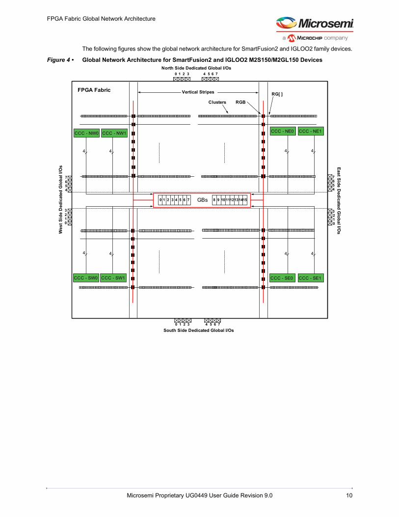
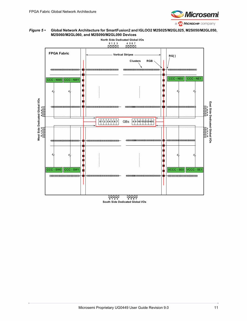
• 2VS16 (2 vertical stripes, 16 GBs)• 1VS8 (1 vertical stripe, 8 GBs)The 2VS16 global network architecture is used for M2S025/M2GL025, M2S050/M2GL050, M2S060/M2GL060, M2S090/M2GL090, and M2S150/M2GL150 devices. The fabric CCCs present on south-east side of the M2S150/M2GL150 devices are replaced with VCCCs on the M2S025/M2GL025, M2S050/M2GL050, M2S060/M2GL060, and M2S090/M2GL090 devices. It supports two vertical stripes, 16 GBs, 32 dedicated global I/Os (8 in each side), and up to eight fabric CCCs (2 in each quadrant).
The 1VS8 global network architecture is used for M2S005/M2GL005 and M2S010/M2GL010 devices, as shown in Figure 6, page 12. It supports 1 vertical stripe, 8 GBs, 16 dedicated global I/Os (4 in each side), and 2 fabric CCCs located in the northeast corner.
The global network is composed of global buffers (GBs) to distribute low-skew clock signals or high-fanout nets. The following figure shows the global signal routing hierarchy to logic clusters. Global signals (G[n:0]) reach the logic clusters through row global signals (RG[7:0]) generated by an associated row global buffer (RGB). RGBs are located on the vertical stripes. RGBs can be accessed from GBs and FPGA fabric routing. GBs can be accessed from dedicated global I/Os, CCC/VCCC global outputs, and the FPGA fabric routing. Clocks coming from regular I/Os can reach GBs or RGBs through FPGA fabric routing.
Table 2 • Maximum Global Resources for SmartFusion2 and IGLOO2 Devices
Resource
SmartFusion2/IGLOO2 Device M2S005 and M2GL005
M2S010 and M2GL010
M2S025 and M2GL025
M2S050 and M2GL050
M2S060 and M2GL060
M2S090 and M2GL090
M2S150 and M2GL150
Fabric CCCs 2 2 6 6 6 6 8
VCCCs 0 0 2 2 2 2 0
Global buffers 8 8 16 16 16 16 16
Dedicated global I/Os 16 16 32 32 32 32 32
FPGA Fabric Global Network Architecture
Microsemi Proprietary UG0449 User Guide Revision 9.0 9
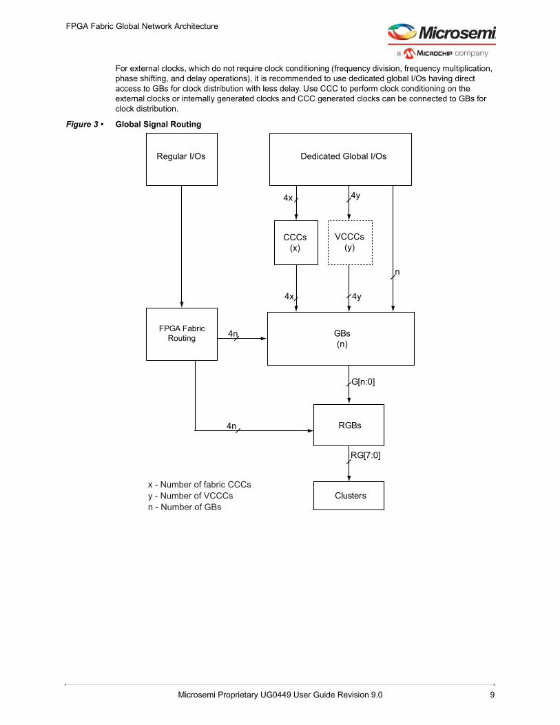
For external clocks, which do not require clock conditioning (frequency division, frequency multiplication, phase shifting, and delay operations), it is recommended to use dedicated global I/Os having direct access to GBs for clock distribution with less delay. Use CCC to perform clock conditioning on the external clocks or internally generated clocks and CCC generated clocks can be connected to GBs for clock distribution.
Figure 3 • Global Signal Routing
GBs(n)
G[n:0]
RG[7:0]
RGBs
Clusters
n
4x
CCCs(x)
VCCCs(y)
4y
4x
4n
4n
4y
FPGA FabricRouting
Regular I/Os Dedicated Global I/Os
x - Number of fabric CCCsy - Number of VCCCsn - Number of GBs
FPGA Fabric Global Network Architecture
Microsemi Proprietary UG0449 User Guide Revision 9.0 10
The following figures show the global network architecture for SmartFusion2 and IGLOO2 family devices.
Figure 4 • Global Network Architecture for SmartFusion2 and IGLOO2 M2S150/M2GL150 Devices
GBs
RGB
RG[ ]
Clusters
Vertical Stripes
0 1 2 3 4 5 6 7 8 9 10 1112131415
0123
North Side Dedicated Global I/OsEast Side D
edicated Global I/O
sWes
t Sid
e D
edic
ated
Glo
bal I
/Os
South Side Dedicated Global I/Os
5
CCC - NW0
CCC - SW0 CCC - SW1 CCC - SE0 CCC - SE1
CCC - NE1CCC - NE0CCC - NW1
44
4 444
4 4
FPGA Fabric
4567
4 6 70 1 2 3
4 5 6 70 1 2 3
0123
4567
FPGA Fabric Global Network Architecture
Microsemi Proprietary UG0449 User Guide Revision 9.0 11
Figure 5 • Global Network Architecture for SmartFusion2 and IGLOO2 M2S025/M2GL025, M2S050/M2GL050, M2S060/M2GL060, and M2S090/M2GL090 Devices
GBs
RGB
RG[ ]
Clusters
Vertical Stripes
0 1 2 3 4 5 6 7 8 9 10 1112131415
0123
5
CCC - NW0 CCC - NW1
CCC - SW1 VCCC - SE0 VCCC - SE1
CCC - NE0 CCC - NE1
CCC - SW0
44
4 444
4 4
FPGA Fabric
4567
4 6 70 1 2 3
4 5 6 70 1 2 3
0123
4567
North Side Dedicated Global I/OsEast Side D
edicated Global I/O
sWes
t Sid
e D
edic
ated
Glo
bal I
/Os
South Side Dedicated Global I/Os

FPGA Fabric Global Network Architecture
Microsemi Proprietary UG0449 User Guide Revision 9.0 12
Figure 6 • Global Network Architecture for SmartFusion2 and IGLOO2 M2S005/M2GL005 and M2S010/M2GL010 Devices
3.1.1 Dedicated Global I/OsSmartFusion2 and IGLOO2 user I/Os are grouped into multi-standard I/Os (MSIO and MSIOD) and DDRIOs. Some of these user I/Os, referred to as dedicated global I/Os, are dual-use I/Os which are capable of driving the global routing network or local routing network. Dedicated global I/Os can be used to bring in external clock signals as inputs to the FPGA fabric. Dedicated global I/Os can be used as regular I/Os, as either input or output for any design signal, if they are not utilized for clocking. Dedicated global I/Os are located on each of the four sides of the FPGA fabric.
Some of the dedicated global I/Os have direct access to GBs, whereas others have to go through either VCCCs or CCCs to reach GBs. Each fabric CCC has four dedicated global I/Os as inputs and can drive up to four GBs. The dedicated global I/Os connect to fabric CCCs, VCCCs, and GBs through a hardwired connection.
GBs
RGB
RG[ ]
Clusters
Vertical Stripe
0 1 2 3 4 5 6
01
3
CCC – NE0 CCC – NE1
4 4
FPGA Fabric
23
20 1
2 30 1
01
23
7
North Side Dedicated Global I/OsEast Side D
edicated Global I/O
sWes
t Sid
e D
edic
ated
Glo
bal I
/Os
South Side Dedicated Global I/Os

FPGA Fabric Global Network Architecture
Microsemi Proprietary UG0449 User Guide Revision 9.0 13
3.1.1.1 Naming Conventions for Dedicated Global I/OsDue to the comprehensive and flexible nature of dedicated global I/Os, a naming scheme is used to provide the detailed information on each I/O.
The dedicated global I/O uses the generic name IOxyBz/GBn/CCCtype_xyz_CLKlw, where
• IO represents the type of I/O: MSIO, MSIOD, or DDRIO.• x represents the I/O pair number.• y represents differential I/O polarity – P (positive) or N (negative).• Bz represents the bank number.• GBn represents dedicated global I/Os that drive the GBs directly, where n is 0 to 15 or 0 to 7.• CCC_xyz_CLKlw represents dedicated global I/Os that drive GBs through CCCs and
VCCC_xyz_CLKl represents dedicated global I/Os that drive GBs through VCCCs, where:• xy represents the location – NE, SW, SE, or NW.• z represents the CCC or VCCC number – 0 or 1.• I represents the clock input• w represents one of the four dedicated global I/Os associated with each CCC: CLKI0, CLKI1,
CLKI2, or CLKI3.Some of the dedicated global I/Os are multiplexed with hard IP blocks such as MSS_MMUART, MSS_I2C, MSS_USB, MSS_GPIO, MDDR, and FDDR. These multiplexed or multi-function dedicated global I/Os act as regular I/Os and cannot be used for accessing the global network or CCCs when the associated hard IP block is enabled in the design. See DS0115: SmartFusion2 Pin Descriptions Datasheet and DS0124: IGLOO2 Pin Descriptions Datasheet for more information on the functions supported by the dedicated global I/Os. The name of a pin shows the functionalities for which that pin can be configured and used.
Example pin name: DDRIO76PB0/GB12/CCC_NE1_CLKI2/MDDR_DQ12
The above example pin is a multi-purpose I/O, which is configured as an MDDR I/O (MDDR_DQ12) when the MDDR is enabled. If MDDR is not used in the design, this I/O can be configured as dedicated global I/O which can drive the CCC_NE1_CLKI2 input port of the CCC_NE1 or GB 12 directly.
Dedicated global I/Os are routed to GBs by the Libero SoC routing software as follows:
• If a dedicated global I/O that has direct access to GBs is selected, the routing software directly routes the dedicated global I/O input to an associated GB.
• If a dedicated global I/O in the east or south side having access to the VCCCs is selected, the routing software routes the dedicated global I/O through the VCCCs to an associated GB.
• If a dedicated global I/O that has direct access to a fabric CCC (CCC macro instantiated in the design with input source selected as dedicated global I/O) is selected, the routing software selects an associated fabric CCC. In this case, the outputs of the fabric CCC reach the associated GBs.
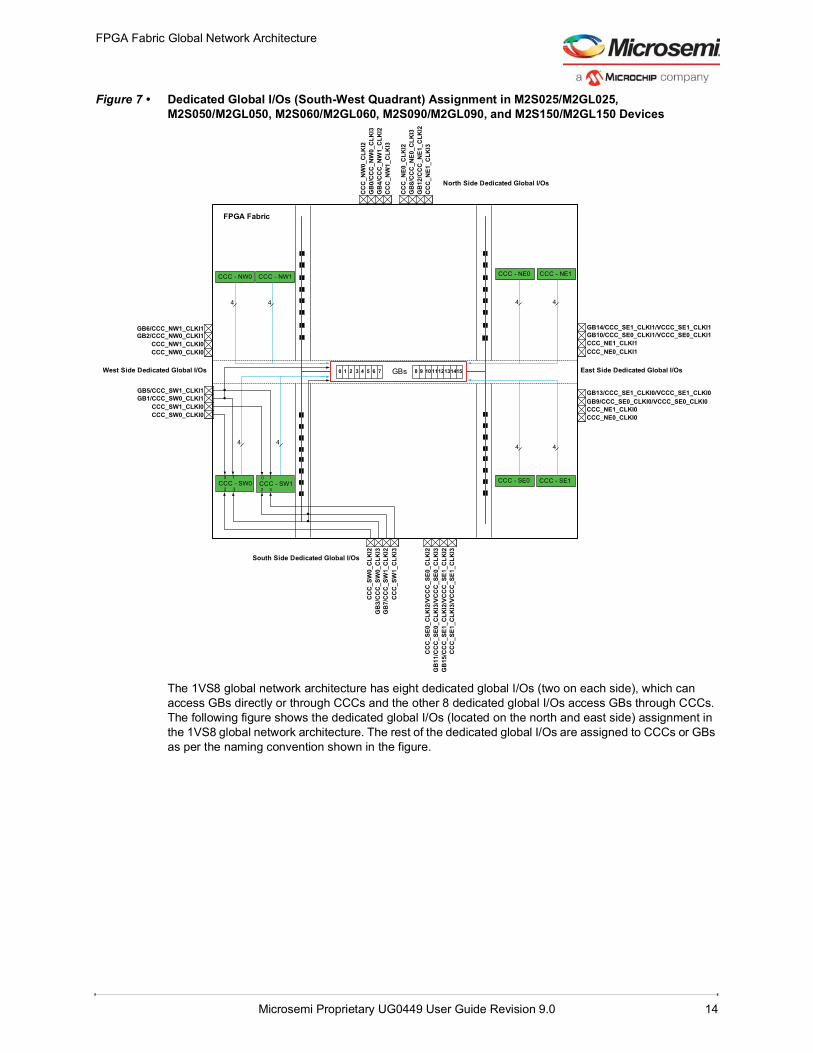
The 2VS16 global network architecture has 16 dedicated global I/Os (4 on each side), which can access GBs directly or through CCCs and the other 16 dedicated global I/Os access GBs through CCCs. The following figure shows the dedicated global I/Os connection for the lower left quadrant of the FPGA fabric in the 2VS16 global network architecture. The rest of the dedicated global I/Os are assigned to CCCs and/or GBs according to the naming convention shown in the figure. The CCC pair present in the southeast corner is replaced by VCCCs for M2S025/M2GL025, M2S050/M2GL050, M2S060/M2GL060, and M2S090/M2GL090 devices.
FPGA Fabric Global Network Architecture
Microsemi Proprietary UG0449 User Guide Revision 9.0 14
Figure 7 • Dedicated Global I/Os (South-West Quadrant) Assignment in M2S025/M2GL025, M2S050/M2GL050, M2S060/M2GL060, M2S090/M2GL090, and M2S150/M2GL150 Devices
The 1VS8 global network architecture has eight dedicated global I/Os (two on each side), which can access GBs directly or through CCCs and the other 8 dedicated global I/Os access GBs through CCCs. The following figure shows the dedicated global I/Os (located on the north and east side) assignment in the 1VS8 global network architecture. The rest of the dedicated global I/Os are assigned to CCCs or GBs as per the naming convention shown in the figure.
GBs0 1 2 3 4 5 6 7 8 9 10 1112131415C
CC
_NW
0_C
LKI2
GB
0/C
CC
_NW
0_C
LKI3
GB
4/C
CC
_NW
1_C
LKI2
CC
C_N
W1_
CLK
I3
CC
C_N
E0_C
LKI2
GB
8/C
CC
_NE0
_CLK
I3G
B12
/CC
C_N
E1_C
LKI2
CC
C_N
E1_C
LKI3
CC
C_S
W0_
CLK
I2G
B3/
CC
C_S
W0_
CLK
I3G
B7/
CC
C_S
W1_
CLK
I2C
CC
_SW
1_C
LKI3
CC
C_S
E0_C
LKI2
/VC
CC
_SE0
_CLK
I2G
B11
/CC
C_S
E0_C
LKI3
/VC
CC
_SE0
_CLK
I3G
B15
/CC
C_S
E1_C
LKI2
/VC
CC
_SE1
_CLK
I2C
CC
_SE1
_CLK
I3/V
CC
C_S
E1_C
LKI3
CCC - NW0 CCC - NW1
CCC - SW0 CCC - SE0 CCC - SE1
CCC - NE1CCC - NE0
44
4 444
4 4
FPGA Fabric
CCC_SW0_CLKI0CCC_SW1_CLKI0
GB1/CCC_SW0_CLKI1GB5/CCC_SW1_CLKI1
CCC_NW0_CLKI0CCC_NW1_CLKI0
GB2/CCC_NW0_CLKI1GB6/CCC_NW1_CLKI1
CCC_NE0_CLKI1CCC_NE1_CLKI1GB10/CCC_SE0_CLKI1/VCCC_SE0_CLKI1GB14/CCC_SE1_CLKI1/VCCC_SE1_CLKI1
CCC_NE0_CLKI0CCC_NE1_CLKI0GB9/CCC_SE0_CLKI0/VCCC_SE0_CLKI0GB13/CCC_SE1_CLKI0/VCCC_SE1_CLKI0
32
0 1CCC - SW1
32
0 1
North Side Dedicated Global I/Os
East Side Dedicated Global I/OsWest Side Dedicated Global I/Os
South Side Dedicated Global I/Os
FPGA Fabric Global Network Architecture
Microsemi Proprietary UG0449 User Guide Revision 9.0 15
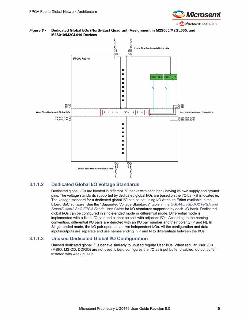
Figure 8 • Dedicated Global I/Os (North-East Quadrant) Assignment in M2S005/M2GL005, and M2S010/M2GL010 Devices
3.1.1.2 Dedicated Global I/O Voltage StandardsDedicated global I/Os are located in different I/O banks with each bank having its own supply and ground pins. The voltage standards supported by dedicated global I/Os are based on the I/O bank it is located in. The voltage standard for a dedicated global I/O can be set using I/O Attribute Editor available in the Libero SoC software. See the "Supported Voltage Standards" table in the UG0445: IGLOO2 FPGA and SmartFusion2 SoC FPGA Fabric User Guide for I/O standards supported by each I/O bank. Dedicated global I/Os can be configured in single-ended mode or differential mode. Differential mode is implemented with a fixed I/O pair and cannot be split with adjacent I/Os. According to the naming convention, differential I/O pairs are denoted with an I/O pair number and their polarity (P and N). In Single-ended mode, the I/O pair operates as two independent I/Os. All the configuration and data inputs/outputs are separate and use names ending in P and N to differentiate between the I/Os.
3.1.1.3 Unused Dedicated Global I/O ConfigurationUnused dedicated global I/Os behave similarly to unused regular User I/Os. When regular User I/Os (MSIO, MSIOD, DDRIO) are not used, Libero configures the I/O as input buffer disabled, output buffer tristated with weak pull-up.
GBs0 1 2 3 4 5 6
CCC_NE1_CLKI1CCC_NE1_CLKI2
CCC – NE0 CCC – NE1
4 4
FPGA Fabric
GB1GB2
CC
C_N
E1_C
LKI3
GB
0
GB
7C
CC
_NE0
_CLK
I0
CC
C_N
E1_C
LKI0
GB
3CCC_NE0_CLKI1CCC_NE0_CLKI2
GB5GB6
7
CC
C_N
E0_C
LKI3
GB
4
1 2
33
North Side Dedicated Global I/Os
East Side Dedicated Global I/OsWest Side Dedicated Global I/Os
South Side Dedicated Global I/Os

FPGA Fabric Global Network Architecture
Microsemi Proprietary UG0449 User Guide Revision 9.0 16
3.1.2 Fabric CCCFabric CCCs enable flexible clocking schemes to the logic implemented in the FPGA fabric, and can also provide the base clock for on-chip hard IP blocks—MSS/HPMS, FDDR, and SERDESIF. Each fabric CCC operates with a dedicated PLL and generates clock signals of varying frequency and phase. Each fabric CCC generates up to four different global clocks (GL0, GL1, GL2, and GL3) and four core clocks (Y0, Y1, Y2, and Y3). The generated global clocks drive GBs and core clocks drive the local routing resources in the FPGA fabric. Fabric CCC's core clock outputs (Yx) can be used to drive internal logic without using global network resources. Core clocks (Yx) introduce additional delay because of FPGA fabric routing. Core clocks are useful when global network resources must be conserved and utilized for other timing-critical paths. The GBs associated with the global clock outputs (GLx) are available to user logic, if the global clock outputs are disabled. Each fabric CCC has four dedicated global I/Os as inputs. Each fabric CCC output (GLx/Yx), as well as the reference clock, can be driven from any one of these four dedicated global I/Os.
Fabric CCCs are labeled according to their location in the FPGA fabric floor plan. For instance, the fabric CCCs located in the northeast corner are labeled CCC-NE0 and CCC-NE1. See the Fabric Clock Conditioning Circuitry, page 39 for more information on fabric CCCs.
3.1.3 VCCCA VCCC is a four-input/four-output crossbar switch (as shown in the following figure). Each VCCC has four inputs that come from the dedicated global I/O pads and can drive up to four GBs. VCCC blocks do not have fabric inputs or outputs and they cannot be connected to each other.
VCCCs are automatically instantiated by the Libero SoC place-and-route tool, based on the dedicated global I/Os utilized to facilitate routing and cannot be instantiated manually into a design. VCCCs are configured with flash bits sets by the Libero SoC software at the time of FPGA fabric programming and cannot be dynamically configured.
Figure 9 • VCCC Functional Block Diagram
3.1.4 Global BufferThe global buffer (GB) is a multiplexer that generates an independent global signal. The GBs can be driven from multiple sources such as dedicated global I/Os, fabric CCCs, VCCCs, and fabric routing. For example, an input signal connected to a dedicated global I/O can route directly to a GB, through a CCC or VCCC. Input signals connected to regular I/Os or any internal logic module can also be connected to the GB through fabric routing. The following figures show sources feeding into GBs, which finally feed into RGBs through G[0-15] to span the complete fabric area.
VCCC
VCCC_SEz_CLKI0
VCCC_SEz_CLKI1
VCCC_SEz_CLKI2
VCCC_SEz_CLKI3
MUX_0
MUX_1
MUX_2
MUX_3
GL0
GL1
GL2
GL3

FPGA Fabric Global Network Architecture
Microsemi Proprietary UG0449 User Guide Revision 9.0 17
GBs can also be fed through regular I/Os, in which case the signals are first routed to fabric routing and then reach the GBs. Any signal generated from logic modules can reach GBs through fabric routing.
Figure 10 • Various Sources Feeding Global Buffers for 2VS16 Global Network Architecture
Figure 11 • Various Sources Feeding Global Buffers for 1VS8 Global Network Architecture
The following table shows the assignment of fabric CCC global outputs (GLx, x = 0 to 3) to the global buffers in the 2VS16 global network architecture. The global outputs of the fabric CCCs, which are present in the west side of the FPGA fabric are mapped to global buffers 0 to 7. The global outputs of the fabric CCCs, which are present in the east side are mapped to global buffers 8 to 15. See Figure 4, page 10 through Figure 6, page 12 for global buffer assignment. Each global output of the fabric CCC is associated with two global buffers. Each global buffer is also shared between one of the four global outputs of four fabric CCCs. For instance, GB0 can be accessed from GL0 of one of the four fabric CCCs present on the west side.
GBs(n)
G[0-15]
LogicElements
DedicatedGlobal I/Os
Regular I/Os
CCCs(x)
FabricRouting
VCCCs(y)
4n
4n
32
GBn
4x 4x
16
4y 4y
CCC_xyz_CLKlw
VCCC_xyz_CLKl
GBs(n)
G[0-7]
DedicatedGlobal I/Os
CCC_xyz_CLKlw CCCs(x)
FabricRouting
4n
16 GBn
4x 4x
8
LUTsRegular I/Os
4n
FPGA Fabric Global Network Architecture
Microsemi Proprietary UG0449 User Guide Revision 9.0 18
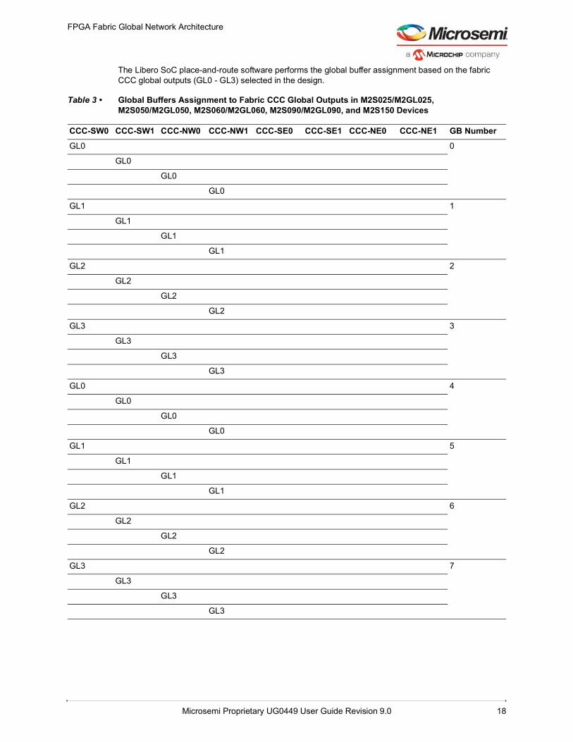
The Libero SoC place-and-route software performs the global buffer assignment based on the fabric CCC global outputs (GL0 - GL3) selected in the design.
Table 3 • Global Buffers Assignment to Fabric CCC Global Outputs in M2S025/M2GL025, M2S050/M2GL050, M2S060/M2GL060, M2S090/M2GL090, and M2S150 Devices
CCC-SW0 CCC-SW1 CCC-NW0 CCC-NW1 CCC-SE0 CCC-SE1 CCC-NE0 CCC-NE1 GB NumberGL0 0
GL0
GL0
GL0
GL1 1
GL1
GL1
GL1
GL2 2
GL2
GL2
GL2
GL3 3
GL3
GL3
GL3
GL0 4
GL0
GL0
GL0
GL1 5
GL1
GL1
GL1
GL2 6
GL2
GL2
GL2
GL3 7
GL3
GL3
GL3

FPGA Fabric Global Network Architecture
Microsemi Proprietary UG0449 User Guide Revision 9.0 19
GL0 8
GL0
GL0
GL0
GL1 9
GL1
GL1
GL1
GL2 10
GL2
GL2
GL2
GL3 11
GL3
GL3
GL3
GL0 12
GL0
GL0
GL0
GL1 13
GL1
GL1
GL1
GL2 14
GL2
GL2
GL2
GL3 15
GL3
GL3
GL3
Table 3 • Global Buffers Assignment to Fabric CCC Global Outputs in M2S025/M2GL025, M2S050/M2GL050, M2S060/M2GL060, M2S090/M2GL090, and M2S150 Devices (continued)
CCC-SW0 CCC-SW1 CCC-NW0 CCC-NW1 CCC-SE0 CCC-SE1 CCC-NE0 CCC-NE1 GB Number

FPGA Fabric Global Network Architecture
Microsemi Proprietary UG0449 User Guide Revision 9.0 20
The following table shows the assignment of fabric CCC global outputs (GLx, x = 0 to 3) to the global buffers in the 1VS8 global network architecture. There is a dedicated global buffer available for each global output of the fabric CCCs.
3.1.5 Row Global BuffersRGBs are situated on the vertical stripes of the global network architecture inside the FPGA fabric. As shown in the following figure, each RGB drives logic clusters, consisting of 12 logic modules, located on left and right branches using Row Globals (RGs). Each cluster consists of 12 logic modules. The global signals from the GBs are routed to RGBs, which are then fed into the clusters through RGs. Each GB has access to all RGBs available on the vertical stripes since the global network is segmented. Each RGB is independent and can be driven by fabric routing in addition to being driven by GBs. This facilitates the use of RGBs to drive regional clocks spanning a small fabric area.
Figure 12 • Row Global Signals Driving Clusters
3.1.6 Clock GatingThe global network has clock gating capability built in to the GBs and RGBs to save power. The clock gating can be enabled by instantiating a global clock buffer macro (GCLKBUF, GCLKBIBUF, GCLKINT, or RGCLKINT) that has a clock input, enable input, and gated clock output or through the advanced tab on the CCC configurator. The following figure shows the clock gating circuit schematic. The place-and-route software maps the instantiated clock buffers to appropriate GBs or RGBs and enables the clock gating capability of the GBs or RGBs. See the Global Macros, page 22 for more information on clock buffer macros available in the IP Catalog of the Libero SoC software.
Table 4 • Global Buffers Assignment to Fabric CCC Global Outputs in M2S005/M2GL005 and M2S010/M2GL010 Devices
CCC- NE1 CCC- NE0 GB NumberGL0 0
GL1 1
GL2 2
GL3 3
GL0 4
GL1 5
GL2 6
GL3 7
{RG[0-7]
RGB
RGB
Clusters Vertical Stripe

FPGA Fabric Global Network Architecture
Microsemi Proprietary UG0449 User Guide Revision 9.0 21
Figure 13 • Clock Gating Circuit Schematic
Clock gating is achieved using a latch and enable (EN), which is driven by the user logic implemented in the FPGA fabric. The latch is transparent when the clock input is in Low phase. The latch is in Hold state when the clock is in High phase. The AND gate at the output allows enabling or disabling of the clock based on the latch output.
• When the EN signal is High, clock is active.• When the EN signal is Low, clock is gated off and drives Low. The following figure shows the timing waveforms for the clock gating enabled clock buffers. SeeDS0128: SmartFusion2 and IGLOO2 Datasheet for the minimum setup and hold time for clock gating enable signal.
Figure 14 • Timing Waveforms for the Clock Gating Circuitry
• If the EN signal changes during the clock High phase and the minimum hold time is met with respect to the prior rising clock edge, the latch output changes after the falling clock edge.
• If the EN signal changes during the clock Low phase and the minimum setup time is met with respect to the next rising clock edge, the latch output will change immediately.
• If the EN signal violates either the setup or hold time with respect to the rising clock edge, the output behavior is unknown.
The CCCs can also produce gated clock output, which can then be fed into the global routing network. Unused global resources such as RGBs and GBs are tied-off automatically to reduce dynamic power consumption.
0D 1EN
Clock
Gated Clock
Clock Gating Circuit Schematic
Latch
Clock
EN
Gated Clock
Latch Output
Hold Time Hold Time Setup TimeSetup Time

FPGA Fabric Global Network Architecture
Microsemi Proprietary UG0449 User Guide Revision 9.0 22
3.2 Design RecommendationsMicrochip recommends that all clocks in a design must be routed using the global routing resources in the device. This ensures that clock skew is minimized throughout the design. Furthermore, global routing resource usage ensures that predictable levels of clock jitter can be accounted for during static timing analysis. This guideline must be applied while selecting clock input pin assignments, selecting CCC reference clock assignments, and generating clocks inside the FPGA. The following sections provide recommendations for using the global network in a design.
3.2.1 Global MacrosGlobal macros can be used for assigning signals to the global network. The CLKBUF, CLKBIBUF, GCLKBUF, and GCLKBIBUF macros allow you to route the clock coming from the dedicated global I/Os to GBs. Selecting the dedicated global I/Os, which are having direct connection to the GBs provide less delay. Dedicated global I/Os, which have direct access to GBs or through VCCCs are available as input pads to these macros. The CLKINT and GCLKINT macros route the internal clock signals or regular I/O signals to GBs through FPGA fabric routing. The RCLKINT and RGCLKINT macros route the internal clock signals to RGBs through FPGA fabric routing. The gated clock buffer macros (GCLKBUF, GCLKBIBUF, GCLKINT, and RGCLKINT) have an FPGA fabric routed control input (EN) to gate off the global clock.
In addition to these global macros, the CCC macro's global outputs (GLx) also drive the GBs. Dedicated global I/Os and their I/O standard can be assigned using I/O Attribute Editor, part of the Libero SoC software. The Libero place-and-route software runs the pre-layout checker and checks the validity of dedicated global I/O assignment.
The following table lists the global macros available for SmartFusion2 and IGLOO2 devices.
Table 5 • Global Macros
Macro Name Description Functional SymbolCLKBUF Macro to drive a clock signal coming from input pad to a global
buffer
CLKBIBUF Macro to drive a clock signal coming from bidirectional I/O pad to a global buffer
CLKINT Macro to drive a global buffer from FPGA fabric routing
GCLKBUF Input macro with control input (EN) to drive or gate off the input clock to a chip-level global net. The clock signal comes from input pad.
CLKBUFPAD Y
CLKBIBUF
PADD E
Y
CLKINTA Y
GCLKBUFPAD Y
EN

FPGA Fabric Global Network Architecture
Microsemi Proprietary UG0449 User Guide Revision 9.0 23
3.2.2 Managing Global SignalsAssigning high fan-out nets to the global clock network is an effective way of reducing routing congestion and minimizing skew. Due to its high propagation delays, the global clock network is not recommended for use in timing-critical data paths.
The clock macros can be used for assigning signals to the global clock network:
• The CLKBUF and CLKBIBUF macro connects a dedicated global I/O to GB. Dedicated global I/Os have direct hardwired routing to GBs.
• The CLKINT macro connects fabric routed signal to GB. The CLKINT macro must be used to connect a regular I/O to GB through the FPGA fabric.
• The RCLKINT macro connects a fabric routed signal to RGB.The CCCs and transceivers drive GBs through hardwired routing.
The Libero SoC software supports automated global buffer allocation to minimize the user intervention. The allocation strategy for global buffers employs the following priority:
• User inserted global macros• Very high fan-out nets• Clock nets• Asynchronous reset/set netsIn Libero tool, the default fan-out threshold for global net promotion is larger for data pins (pins involved in register-to-register paths) than asynchronous logic pins (pins involved in register-to-asynchronous paths).
Due to this, the automated design flow is more likely to employ global nets on register-to-asynchronous paths than register-to-register paths. The reasoning for this is that asynchronous pins are not normally timing-critical, and routing them on global nets reduce routing congestion. However, register-to asynchronous paths are functionally equivalent to register-to-register paths from the perspective of achieving timing closure. As a result, when designing register-to-asynchronous paths, ensure that timing critical connections do not unnecessarily employ global nets.
GCLKBIBUF Bidirectional macro with control input (EN) to drive or gate off the input clock to a chip-level global net. The clock signal comes from bidirectional I/O pad.
GCLKINT Macro with control input (EN) to drive or gate off the input clock to a chip-level global net; input clock is routed through FPGA fabric.
RCLKINT Macro to drive a row global net from FPGA fabric.
RGCLKINT Macro with control input (EN) to drive or gate off the input clock to a row global net; input clock is routed through FPGA fabric.
Table 5 • Global Macros (continued)
Macro Name Description Functional Symbol
GCLKBIBUF
PADD E
EN
Y
GCLKINTA
EN
Y
RCLKINTA Y
RGCLKINTA
EN
Y
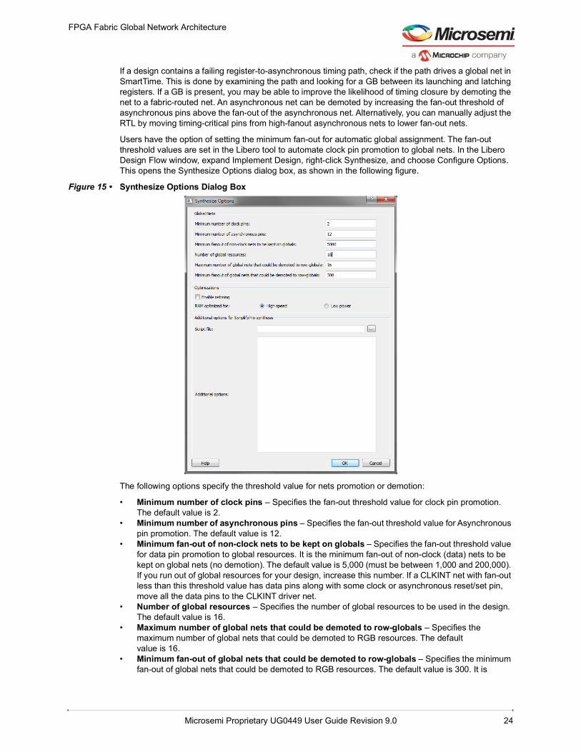
FPGA Fabric Global Network Architecture
Microsemi Proprietary UG0449 User Guide Revision 9.0 24
If a design contains a failing register-to-asynchronous timing path, check if the path drives a global net in SmartTime. This is done by examining the path and looking for a GB between its launching and latching registers. If a GB is present, you may be able to improve the likelihood of timing closure by demoting the net to a fabric-routed net. An asynchronous net can be demoted by increasing the fan-out threshold of asynchronous pins above the fan-out of the asynchronous net. Alternatively, you can manually adjust the RTL by moving timing-critical pins from high-fanout asynchronous nets to lower fan-out nets.
Users have the option of setting the minimum fan-out for automatic global assignment. The fan-out threshold values are set in the Libero tool to automate clock pin promotion to global nets. In the Libero Design Flow window, expand Implement Design, right-click Synthesize, and choose Configure Options. This opens the Synthesize Options dialog box, as shown in the following figure.
Figure 15 • Synthesize Options Dialog Box
The following options specify the threshold value for nets promotion or demotion:
• Minimum number of clock pins – Specifies the fan-out threshold value for clock pin promotion. The default value is 2.
• Minimum number of asynchronous pins – Specifies the fan-out threshold value for Asynchronous pin promotion. The default value is 12.
• Minimum fan-out of non-clock nets to be kept on globals – Specifies the fan-out threshold value for data pin promotion to global resources. It is the minimum fan-out of non-clock (data) nets to be kept on global nets (no demotion). The default value is 5,000 (must be between 1,000 and 200,000). If you run out of global resources for your design, increase this number. If a CLKINT net with fan-out less than this threshold value has data pins along with some clock or asynchronous reset/set pin, move all the data pins to the CLKINT driver net.
• Number of global resources – Specifies the number of global resources to be used in the design. The default value is 16.
• Maximum number of global nets that could be demoted to row-globals – Specifies the maximum number of global nets that could be demoted to RGB resources. The default value is 16.
• Minimum fan-out of global nets that could be demoted to row-globals – Specifies the minimum fan-out of global nets that could be demoted to RGB resources. The default value is 300. It is

FPGA Fabric Global Network Architecture
Microsemi Proprietary UG0449 User Guide Revision 9.0 25
undesirable to have high fan-out clock nets demoted using RGB resources because it may result in high skew. If you run out of global resources for your design, reduce this number to allow more globals to be demoted to RGB resources.
Note: Hardwired connections to global resources, such as connections from CCCs and Dedicated Global I/Os cannot be controlled by synthesize options.
After synthesis, the compiler tool performs the following steps to assign nets to global buffers:
1. Sorting all CLKINT nets in the following priority order.• Fan-out, only if fan-out threshold value specified by minimum fanout of non-clock nets to be
kept on globals • Number of clock pins • Number of asynchronous reset/set pins • Number of data pins
2. Determining the number of GB resources available for CLKINT nets after allocating them to CLKBUF and CLKBIBUF.
3. Demoting CLKINT nets from the sorted list that are beyond the limit specified by the number of global resources. • If such a net has at least the number of pins specified by minimum fanout of global nets that
could be demoted to row-globals, replace the CLKINT with an RCLKINT macro. Limit the number of nets demoted to RCLKINT to the count specified by maximum number of global nets that could be demoted to row-globals.
• Otherwise, merge the net with the driver of the CLKINT. The HDL source file or SmartDesign schematic is the preferred place for defining which signals must be assigned to a global network using global macro instantiation. A signal with high-fanout may have logic replication, if it is not promoted to a global during synthesis.
3.2.3 Place and RoutePlace and Route step aligns placement of I/Os, CCC, and GB resources while preserving any user locked placement, finding feasible I/O bank technology solution and optimizing the number of hardwired connections to reduce clock insertion delays. An I/O may be hardwired to a GB as well as route directly to data pins in the fabric.
The RCLKINT/RGCLKINT nets are mapped to RGB resources with routed inputs and the placement algorithm resolves the RGB bandwidth per row. The algorithm contains a cost structure to penalize over subscription of RGB resources per row beyond the limit of 8. Increasing the number of globals and local clock nets therefore adversely impact the runtime.
The power-driven option optimizes the number of rows occupied by a global net or a local clock net, resulting drop in performance (on average).
After performing the place and route, a report of global nets is generated. User can open the report tab to view the global net report. The user must review the generated global net report to understand and minimize clocks that are routed on FPGA fabric routing instead of global routing resources. The following figures show an example of global net report.
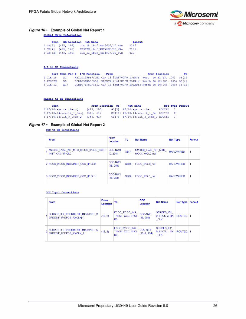
FPGA Fabric Global Network Architecture
Microsemi Proprietary UG0449 User Guide Revision 9.0 26
Figure 16 • Example of Global Net Report 1
Figure 17 • Example of Global Net Report 2

FPGA Fabric Global Network Architecture
Microsemi Proprietary UG0449 User Guide Revision 9.0 27
Figure 18 • Example of Global Net Report 3

On-Chip Oscillators
Microsemi Proprietary UG0449 User Guide Revision 9.0 28
4 On-Chip Oscillators
SmartFusion2 and IGLOO2 devices have the following on-chip oscillators for generating free-running clocks:
• 1 MHz RC Oscillator• 50 MHz RC Oscillator• Main Crystal Oscillator• Auxiliary Crystal OscillatorFigure 19, page 28 and Figure 20, page 29 show clock sourcing capabilities of the SmartFusion2 and IGLOO2 on-chip oscillators. On-chip oscillators can provide reference clock input to the following resources:
• Fabric CCCs• User logic in the FPGA fabric through fabric routing• MSS RTC (available only in the SmartFusion2 device)• MSS and HPMS during Flash*Freeze modeThe auxiliary crystal oscillator is available only in SmartFusion2 devices and is dedicated for MSS RTC clocking as an alternative clock source. SmartFusion2 M2S050 devices do not have an auxiliary crystal oscillator.
The on-chip oscillators also supply clocks to hard IP blocks such as the system controller and POR circuitry. This chapter describes the on-chip oscillator's clock sourcing capabilities and use models. See the "On-Chip Oscillators" section in the DS0128: SmartFusion2 and IGLOO2 Datasheet for the electrical characteristics of on-chip oscillators.
Figure 19 • SmartFusion2 On-Chip Oscillators Clock Sourcing Capabilities
CLKx
Yx
GLx
4
4
4
3
3
CCC_xyz_CLKl0
CCC_xyz_CLKl1
CCC_xyz_CLKl2
CCC_xyz_CLKl3
User Logic
MSSSub-blocks
RTC_CLK RTC
XTLOSC_RTC_CLK
MSS
SmartFusion2 SoC FPGA
FPGA Fabric
MSS CCC
FACCMPLL
RCOSC_50 MHz
RCOSC_1 MHz
XTLOSC_CLK
FabricCCC(s)
PLL
Auxilary CrystalOscillator
(32 KHz - 20 MHz)
50 MHzRC Oscillator
1 MHzRC Oscillator
Main CrystalOscillator
(32 KHz - 20 MHz)
SystemController
PORCircuitry
WDT
COMM_BLK
XTLOSC_MAIN_XTAL
XTLOSC_AUX_XTAL
XTLOSC_MAIN_EXTAL
XTLOSC_AUX_EXTAL

On-Chip Oscillators
Microsemi Proprietary UG0449 User Guide Revision 9.0 29
Figure 20 • IGLOO2 On-Chip Oscillators Clock Sourcing Capabilities
4.1 Functional DescriptionThe outputs of on-chip oscillators are connected to the fabric CCCs, MSS/HPMS CCC, and hard IP blocks through dedicated hardwired connections (not routed through FPGA fabric). The on-chip oscillators can be configured by Chip Oscillators macro in the Libero SoC software to drive user logic and/or fabric CCCs. Unused on-chip oscillators are automatically disabled by the Libero SoC design software if neither of their outputs are enabled. The oscillator is turned off synchronously without generating runt clock pulses.
4.1.1 1 MHz RC OscillatorThe 1 MHz RC oscillator generates a nominal 1 MHz digital clock signal. It is powered by the device core supply VDD and does not require external components for operation.
The 1 MHz RC oscillator can be configured as a clock source to the following:
• Fabric CCCs• User logic in the FPGA fabric through fabric routing• MSS RTC (SmartFusion2 only)• MSS and HPMS during Flash*Freeze modeDuring device power-up, it provides the clock to the POR circuitry through a dedicated connection to determine the duration of POR signal assertion.
CLKx
Yx
GLx
4
4
4
3
3
CCC_xyz_CLKl0
CCC_xyz_CLKl1
CCC_xyz_CLKl2
CCC_xyz_CLKl3
User Logic
HPMSSub-blocks
HPMS
IGLOO2
Fabric
HPMS CCC
FACCMPLL
RCOSC_50 MHz
RCOSC_1 MHz
XTLOSC_CLK
FabricCCC(s)
PLL
50 MHzRC Oscillator
1 MHzRC Oscillator
Main CrystalOscillator
(32 KHz - 20 MHz)
SystemController
PORCircuitry
COMM_BLK
XTLOSC_MAIN_XTAL XTLOSC_MAIN_EXTAL
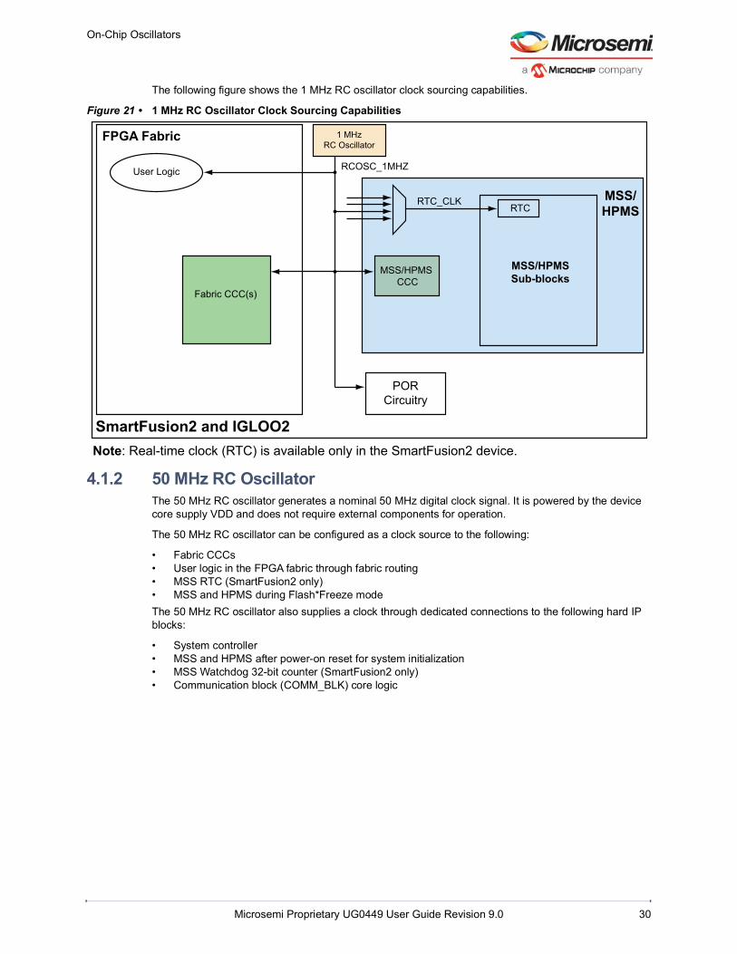
On-Chip Oscillators
Microsemi Proprietary UG0449 User Guide Revision 9.0 30
The following figure shows the 1 MHz RC oscillator clock sourcing capabilities.
Figure 21 • 1 MHz RC Oscillator Clock Sourcing Capabilities
4.1.2 50 MHz RC OscillatorThe 50 MHz RC oscillator generates a nominal 50 MHz digital clock signal. It is powered by the device core supply VDD and does not require external components for operation.
The 50 MHz RC oscillator can be configured as a clock source to the following:
• Fabric CCCs• User logic in the FPGA fabric through fabric routing• MSS RTC (SmartFusion2 only)• MSS and HPMS during Flash*Freeze mode The 50 MHz RC oscillator also supplies a clock through dedicated connections to the following hard IP blocks:
• System controller• MSS and HPMS after power-on reset for system initialization• MSS Watchdog 32-bit counter (SmartFusion2 only)• Communication block (COMM_BLK) core logic
User Logic
MSS/HPMSSub-blocks
RTC_CLK
RCOSC_1MHZ
RTCMSS/HPMS
SmartFusion2 and IGLOO2
FPGA Fabric
MSS/HPMS CCC
PORCircuitry
Fabric CCC(s)
1 MHzRC Oscillator
Note: Real-time clock (RTC) is available only in the SmartFusion2 device.

On-Chip Oscillators
Microsemi Proprietary UG0449 User Guide Revision 9.0 31
The following figure shows the 50 MHz RC oscillator clock sourcing capabilities.
Figure 22 • 50 MHz RC Oscillator Clock Sourcing Capabilities
4.1.3 Main Crystal OscillatorThe main crystal oscillator works with an external crystal, ceramic resonator, or a resistor-capacitor (RC) network to generate a high-precision clock in the range of 32 KHz to 20 MHz. The main crystal oscillator has two I/O pads, XTLOSC_MAIN_EXTAL and XTLOSC_MAIN_XTAL, which can be connected to a crystal, a ceramic resonator, or an RC circuit. If the main crystal oscillator is not used, the XTLOSC_MAIN_EXTAL and XTLOSC_MAIN_XTAL pins can be left floating. The following table shows the output frequency range of the main crystal oscillator with different possible sources.
The main crystal oscillator can be configured as a clock source to the following:
• Fabric CCCs • User logic in the FPGA fabric through fabric routing• MSS RTC (SmartFusion2 only)
• To generate a real-time clock using the MSS RTC, Microsemi recommends using the main crystal oscillator or auxiliary crystal oscillator (if present) with an external crystal as the MSS RTC clock source. RTC is available only in the SmartFusion2 device.
Table 6 • Main Crystal Oscillator Output Frequency Range
Source Output Frequency RangeCrystal 32 KHz to 20 MHz
RC Circuit 32 KHz to 4 MHz
Ceramic Resonator 500 KHz to 4 MHz
User Logic
MSS/HPMSSub-blocks
RTC_CLK
RCOSC_50MHZ
RTC
WDT
COMM_BLK
MSS/HPMS
SmartFusion2 and IGLOO2
FPGA Fabric
MSS/HPMS CCC
SystemController
Fabric CCC(s)
50 MHzRC Oscillator
Note: RTC and Watchdog counter are available only in the SmartFusion2 device.

On-Chip Oscillators
Microsemi Proprietary UG0449 User Guide Revision 9.0 32
The following figure shows the main crystal oscillator clock sourcing capabilities.
Figure 23 • Main Crystal Oscillator Clock Sourcing Capabilities
The main crystal oscillator supports the four modes of operation as defined in the following table. The operating mode of the main crystal oscillator is automatically selected by the Chip Oscillators macro available in the IP Catalog of the Libero SoC design software based on the oscillator source and output frequency.
Table 7 • Main Crystal Oscillator Operational Modes
Oscillator Mode Frequency Range Oscillator Source DescriptionRC network 32 KHz to 4 MHz RC network RC network mode. R and C are connected at
XTLOSC_MAIN_EXTAL pad.
Low gain 32 KHz to 75 KHz Crystal Low power or Low frequency mode. Oscillator consumes the least current of the three modes with a crystal connected to I/O pads.
Medium gain 75 KHz to 2 MHz Crystal or ceramic resonator
Medium power or Medium frequency mode of the three modes with a crystal or ceramic resonator connected to I/O pads.
High gain 2 MHz to 20 MHz Crystal High power or High frequency mode. Consumes the maximum current of the three modes with a crystal connected to I/O pads.
User Logic
MSS/HPMSSub-blocks
RTC_CLK
MAIN_XTLOSC_CLK
RTCMSS/HPMS
SmartFusion2 and IGLOO2
FPGA Fabric
MSS/HPMS CCC
Fabric CCC(s)
Main CrystalOscillator
XTLOSC_MAIN_XTAL XTLOSC_MAIN_EXTAL
Note: RTC is available only in the SmartFusion2 device.

On-Chip Oscillators
Microsemi Proprietary UG0449 User Guide Revision 9.0 33
4.1.3.1 RC Network ModeThe frequency generated by the main crystal oscillator in RC network mode is determined by the RC time constant of the selected R and C components. The R and C components are connected to the XTLOSC_MAIN_EXTAL pin, with the XTLOSC_MAIN_XTAL pin tied to the power pin, VPP, as shown in the following figure.
Figure 24 • Main Crystal Oscillator in RC Network Mode
4.1.3.2 Crystal/Ceramic Resonator ModesIn crystal/ceramic resonator modes, the main crystal oscillator is configured to support an external crystal or ceramic resonator connected between the XTLOSC_MAIN_EXTAL and XTLOSC_MAIN_XTAL pins. The main crystal oscillator can operate in Low Gain, Medium Gain, or High Gain mode when a crystal is connected between the XTLOSC_MAIN_EXTAL and XTLOSC_MAIN_XTAL pins. The main crystal oscillator operates in Medium Gain mode when a ceramic resonator is connected between the XTLOSC_MAIN_EXTAL and XTLOSC_MAIN_XTAL pins. Additionally, a capacitor is required on both XTLOSC_MAIN_EXTAL and XTLOSC_MAIN_XTAL pins to ground, as shown in the following figure. These capacitance values are specific to crystal/ceramic and are vendor specific. Most of the commercially available crystals/ceramic resonators operate in parallel resonant frequency mode. In such cases, the vendor also specifies a load capacitance value which must be connected at XTLOSC_MAIN_EXTAL and XTLOSC_MAIN_XTAL pins (C1 and C2).
Off-chip
R
C
VPP
XTLOSC_MAIN_EXTAL
XTLOSC_MAIN_XTAL
VSS
CLKOUTMain CrystalOscillator

On-Chip Oscillators
Microsemi Proprietary UG0449 User Guide Revision 9.0 34
The following figure shows a main crystal oscillator in ceramic or crystal resonator mode.
Figure 25 • Main Crystal Oscillator in Ceramic Resonator or Crystal Mode
Typically, designers choose the values of capacitors C1 and C2 to match the crystal CL using the below equation:
CL is the load capacitance provided in manufacturer datasheet.
CS is stray capacitance on the PCB and this can be assumed to be in the range of 2 to 5 pF.
Usually C1 and C2 are selected such that they are equal.
Note: The preceding equation is only a guideline, and selection of Capacitors depends on design requirements like cost, availability, frequency accuracy, PPM, and type of application etc.
Large values of C1 and C2, increases the frequency stability but decrease the loop gain and may cause oscillator startup problems. The basic rule of thumb is “value of C1 and C2 is twice as CL“. However, the values of C1 and C2 depends on design requirements.
See DS0128: SmartFusion2 and IGLOO2 Datasheet for more information on external component selection for the main crystal oscillator.
4.1.4 Auxiliary Crystal Oscillator Auxiliary crystal oscillator is available only in the SmartFusion2 device. SmartFusion2 devices, except M2S050, have an auxiliary crystal oscillator dedicated to MSS RTC clocking as an alternative clock source. The MSS RTC generates a real-time clock by taking input from the auxiliary crystal oscillator when the main crystal oscillator is being used for another purpose.
Similar to the main crystal oscillator, the auxiliary crystal oscillator works with an external crystal, ceramic resonator, or an RC circuit to generate a high-precision clock in the range of 32 KHz to 20 MHz. The auxiliary crystal oscillator has two I/O pads, XTLOSC_AUX_EXTAL and XTLOSC_AUX_XTAL, which can be connected to a crystal, a ceramic resonator, or an RC circuit. If the main crystal oscillator is not used, the XTLOSC_MAIN_EXTAL and XTLOSC_MAIN_XTAL pins can be left floating. The output frequency range, operating modes, and characteristics of the auxiliary crystal oscillator are the same as those of the main crystal oscillator. For more information, see Table 6, page 31 and Table 7, page 32.
Table 8 • Example Crystal Oscillators
Part Number Manufacturer DescriptionCM519-32.768KEZF-UT Citizen CRYSTAL 32.768 kHz 12.5 pF SMD
ECS-32.7-12.5-34B-C-TR ECS Inc
ABS10-32.768KHz-1-T Abracon LLC
Off-Chip
C1 C2
XTLOSC_MAIN_EXTAL
XTLOSC_MAIN_XTAL
VSS
CLKOUTMain CrystalOscillator
CLC1 C2C1 C2------------------- CS+=
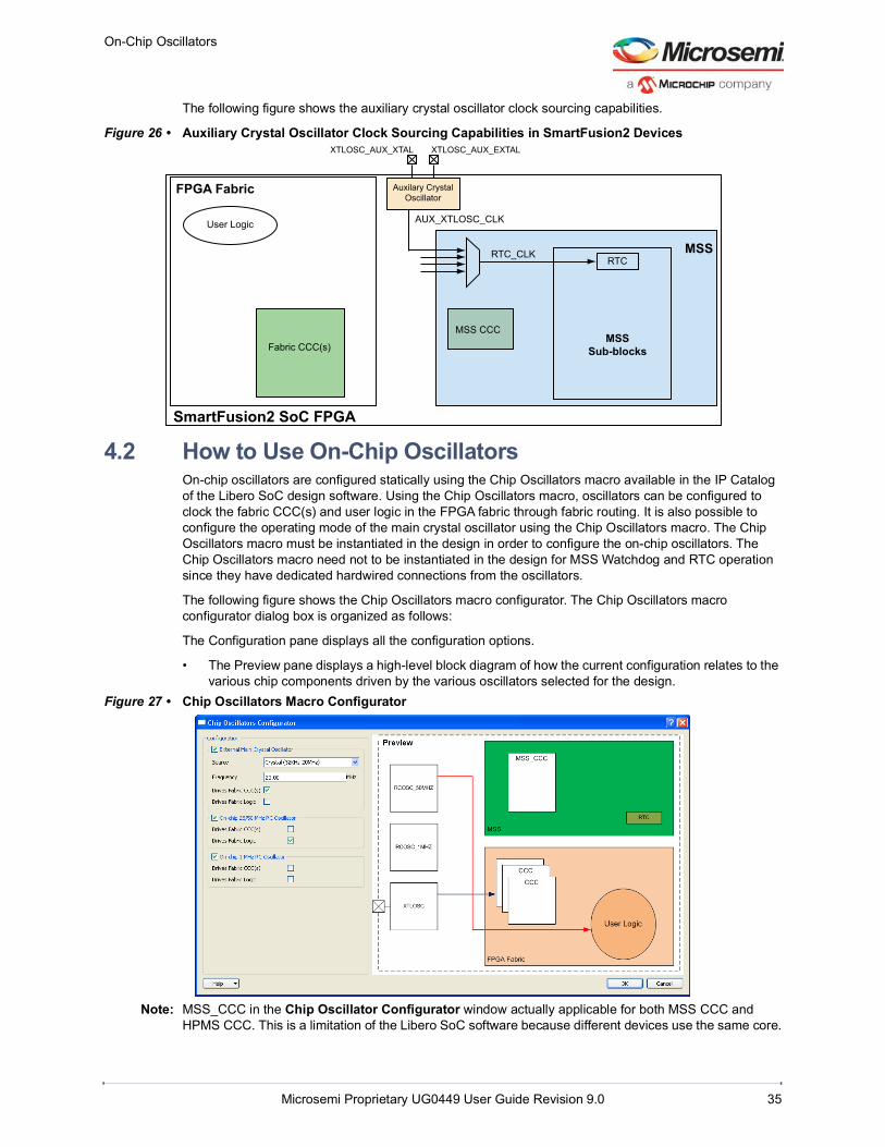
On-Chip Oscillators
Microsemi Proprietary UG0449 User Guide Revision 9.0 35
The following figure shows the auxiliary crystal oscillator clock sourcing capabilities.
Figure 26 • Auxiliary Crystal Oscillator Clock Sourcing Capabilities in SmartFusion2 Devices
4.2 How to Use On-Chip OscillatorsOn-chip oscillators are configured statically using the Chip Oscillators macro available in the IP Catalog of the Libero SoC design software. Using the Chip Oscillators macro, oscillators can be configured to clock the fabric CCC(s) and user logic in the FPGA fabric through fabric routing. It is also possible to configure the operating mode of the main crystal oscillator using the Chip Oscillators macro. The Chip Oscillators macro must be instantiated in the design in order to configure the on-chip oscillators. The Chip Oscillators macro need not to be instantiated in the design for MSS Watchdog and RTC operation since they have dedicated hardwired connections from the oscillators.
The following figure shows the Chip Oscillators macro configurator. The Chip Oscillators macro configurator dialog box is organized as follows:
The Configuration pane displays all the configuration options.
• The Preview pane displays a high-level block diagram of how the current configuration relates to the various chip components driven by the various oscillators selected for the design.
Figure 27 • Chip Oscillators Macro Configurator
Note: MSS_CCC in the Chip Oscillator Configurator window actually applicable for both MSS CCC and HPMS CCC. This is a limitation of the Libero SoC software because different devices use the same core.
User Logic
MSSSub-blocks
RTC_CLK
AUX_XTLOSC_CLK
RTCMSS
SmartFusion2 SoC FPGA
FPGA Fabric
MSS CCC
Fabric CCC(s)
Auxilary CrystalOscillator
XTLOSC_AUX_EXTALXTLOSC_AUX_XTAL

On-Chip Oscillators
Microsemi Proprietary UG0449 User Guide Revision 9.0 36
The following steps must be followed for each oscillator to use in the design:
1. Select the oscillator(s) by selecting the appropriate check box.Figure 28 • Select the Oscillator(s)
2. If Main Crystal Oscillator is selected, its source and frequency must be configured. 3. Select the resource type—Fabric CCC and/or Fabric Logic—to which the selected oscillator(s) will
be connected.Figure 29 • Select the On-chip Oscillator(s) Resource Type
For each type of oscillator configured, a port will be exposed on the instance of the Chip Oscillators macro. Each exposed port can only be connected in SmartDesign to a port that matches the type of connection (oscillator and connectivity type) implied by the configuration made in the Chip Oscillators macro. For instance, if a fabric CCC is configured to use the main crystal oscillator, the input port exposed on the CCC for the main crystal oscillator—XTLOSC_CCC_IN—can only be driven by the output port—XTLOSC_CCC_OUT—of the Chip Oscillators macro.
Figure 30 • Main Crystal Oscillator and Fabric CCC Connectivity
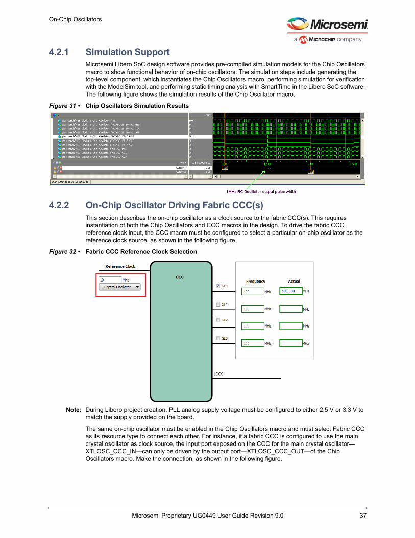
On-Chip Oscillators
Microsemi Proprietary UG0449 User Guide Revision 9.0 37
4.2.1 Simulation SupportMicrosemi Libero SoC design software provides pre-compiled simulation models for the Chip Oscillators macro to show functional behavior of on-chip oscillators. The simulation steps include generating the top-level component, which instantiates the Chip Oscillators macro, performing simulation for verification with the ModelSim tool, and performing static timing analysis with SmartTime in the Libero SoC software. The following figure shows the simulation results of the Chip Oscillator macro.
Figure 31 • Chip Oscillators Simulation Results
4.2.2 On-Chip Oscillator Driving Fabric CCC(s) This section describes the on-chip oscillator as a clock source to the fabric CCC(s). This requires instantiation of both the Chip Oscillators and CCC macros in the design. To drive the fabric CCC reference clock input, the CCC macro must be configured to select a particular on-chip oscillator as the reference clock source, as shown in the following figure.
Figure 32 • Fabric CCC Reference Clock Selection
Note: During Libero project creation, PLL analog supply voltage must be configured to either 2.5 V or 3.3 V to match the supply provided on the board.
The same on-chip oscillator must be enabled in the Chip Oscillators macro and must select Fabric CCC as its resource type to connect each other. For instance, if a fabric CCC is configured to use the main crystal oscillator as clock source, the input port exposed on the CCC for the main crystal oscillator—XTLOSC_CCC_IN—can only be driven by the output port—XTLOSC_CCC_OUT—of the Chip Oscillators macro. Make the connection, as shown in the following figure.

On-Chip Oscillators
Microsemi Proprietary UG0449 User Guide Revision 9.0 38
The same main crystal oscillator can also source the reference clock to multiple fabric CCCs instantiated in the design.
Figure 33 • Main Crystal Oscillator Driving Fabric CCC
4.2.3 On-Chip Oscillator Driving User Logic This section describes the on-chip oscillator as a clock source to the user logic implemented in the FPGA fabric. This requires instantiation of the Chip Oscillators macro in the design. To drive user logic clock input directly, the Chip Oscillators macro must be configured to enable required on-chip oscillator(s) and must select Fabric Logic as the resource type. For instance, if you configure the Chip Oscillators macro to use the 50 MHz RC oscillator as a clock source for the user logic, the clock port exposed on the user logic can be driven by the output port—RCOSC_25_50MHz _O2F—of the Chip Oscillators macro, either directly or through the CLKINT macro. Microsemi recommends connecting the selected on-chip oscillator's output through a CLKINT clock macro to route the clock over the global network. Make the connections, as shown in the following figure.
Figure 34 • 50 MHz RC Oscillator Driving User Logic
4.2.4 MSS RTC Clock Source Selection This section describes the selection of the MSS RTC clock source from one of the on-chip oscillators. This requires instantiation of the MSS component in the design. The MSS_RTC instance in the MSS configurator must be configured to select the clock source for the MSS RTC, as shown in the following figure.
Note: MSS RTC is available only in the SmartFusion2 device.
Note: To generate a real-time clock using the MSS RTC, Microsemi recommends using either the main crystal oscillator or auxiliary crystal oscillator (if present) with an external crystal as the MSS RTC clock source.
Figure 35 • MSS RTC Configurator – MSS RTC Clock Source Selection

Fabric Clock Conditioning Circuitry
Microsemi Proprietary UG0449 User Guide Revision 9.0 39
5 Fabric Clock Conditioning Circuitry
SmartFusion2 and IGLOO2 devices have two, six, or eight fabric CCCs. Each fabric CCC enables flexible clocking schemes for the logic implemented in the FPGA fabric and can provide the base clock for on-chip hard IP blocks—MSS/HPMS, FDDR, and SERDESIF. Each fabric CCC operates with a dedicated PLL and can generate clock signals of different frequency and phase. The associated PLL can be bypassed if it is not required. This chapter describes the fabric CCC features, configuration, and use models.The following table lists the number of fabric CCCs available in SmartFusion2 and IGLOO2 devices.
5.1 FeaturesEach fabric CCC supports the following features:
• Internal and external clock sources• Generation of four different clocks with a maximum frequency up to 400 MHz
• Drives global network and/or the local routing network• Automatic output resynchronization after PLL lock• Configurable phase error window for PLL lock assertion• Configurable PLL lock delay• Spread spectrum clock generation (SSCG)• Dynamic clock switching without any glitches• Clock delay or clock advancement• Clock phase shifting• Clock inversion• Clock holding• Clock gating
Table 9 • Number of Fabric CCCs in SmartFusion2 and IGLOO2 Devices
Resource SmartFusion2 and IGLOO2 Device Part NumberM2S005
and M2GL005
M2S010 and
M2GL010
M2SL025 and
M2GL025
M2SL050 and
M2GL050
M2SL060 and
M2GL060
M2S090 and
M2GL090
M2S150 and
M2GL150Fabric CCCs1
1. Each fabric CCC has a dedicated PLL for clock synchronization and clock synthesis.
2 2 6 6 6 6 8
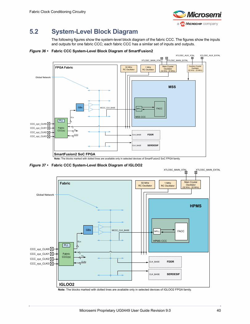
Fabric Clock Conditioning Circuitry
Microsemi Proprietary UG0449 User Guide Revision 9.0 40
5.2 System-Level Block DiagramThe following figures show the system-level block diagram of the fabric CCC. The figures show the inputs and outputs for one fabric CCC; each fabric CCC has a similar set of inputs and outputs.
Figure 36 • Fabric CCC System-Level Block Diagram of SmartFusion2
Figure 37 • Fabric CCC System-Level Block Diagram of IGLOO2
CLKx
Yx
GLx
4
4
4
3
CCC_xyz_CLKl0
CCC_xyz_CLKl1
CCC_xyz_CLKl2
CCC_xyz_CLKl3
Global Network
MCCC_CLK_BASE
MSS
SmartFusion2 SoC FPGA
FPGA Fabric
XTLOSC_MAIN_XTAL
XTLOSC_AUX_XTAL
XTLOSC_MAIN_EXTAL
XTLOSC_AUX_EXTAL
Note: The blocks marked with dotted lines are available only in selected devices of SmartFusion2 SoC FPGA family.
MSS CCC
FACCMPLL
CLK_BASE
CLK_BASE
SERDESIF
FDDR
FabricCCC(s)
PLL
GBs
Auxilary CrystalOscillator
(32 KHz - 20 MHz)
50 MHzRC Oscillator
1 MHzRC Oscillator
Main CrystalOscillator
(32 KHz - 20 MHz)
CLKx
Yx
GLx
4
4
4
3
CCC_xyz_CLKl0
CCC_xyz_CLKl1
CCC_xyz_CLKl2
CCC_xyz_CLKl3
Global Network
MCCC_CLK_BASE
HPMS
IGLOO2
Fabric
Note: The blocks marked with dotted lines are available only in selected devices of IGLOO2 FPGA family.
HPMS CCC
FACCMPLL
CLK_BASE
CLK_BASE
SERDESIF
FDDR
FabricCCC(s)
PLL
GBs
50 MHzRC Oscillator
1 MHzRC Oscillator
Main CrystalOscillator
(32 KHz - 20 MHz)
XTLOSC_MAIN_XTAL XTLOSC_MAIN_EXTAL
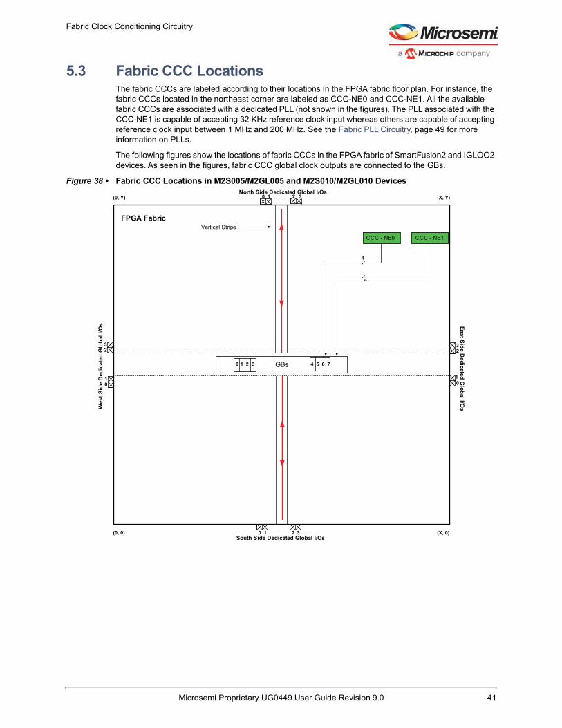
Fabric Clock Conditioning Circuitry
Microsemi Proprietary UG0449 User Guide Revision 9.0 41
5.3 Fabric CCC LocationsThe fabric CCCs are labeled according to their locations in the FPGA fabric floor plan. For instance, the fabric CCCs located in the northeast corner are labeled as CCC-NE0 and CCC-NE1. All the available fabric CCCs are associated with a dedicated PLL (not shown in the figures). The PLL associated with the CCC-NE1 is capable of accepting 32 KHz reference clock input whereas others are capable of accepting reference clock input between 1 MHz and 200 MHz. See the Fabric PLL Circuitry, page 49 for more information on PLLs.
The following figures show the locations of fabric CCCs in the FPGA fabric of SmartFusion2 and IGLOO2 devices. As seen in the figures, fabric CCC global clock outputs are connected to the GBs.
Figure 38 • Fabric CCC Locations in M2S005/M2GL005 and M2S010/M2GL010 Devices
GBs
Vertical Stripe
0 1 2 3
01
23
North Side Dedicated Global I/Os
South Side Dedicated Global I/Os
Wes
t Sid
e D
edic
ated
Glo
bal I
/Os East Side D
edicated Global I/O
s
0 1 2 3
01
23
0 1 2 3
4 5 6 7
4
4
FPGA Fabric
CCC - NE0 CCC - NE1
(0, Y) (X, Y)
(X, 0)(0, 0)

Fabric Clock Conditioning Circuitry
Microsemi Proprietary UG0449 User Guide Revision 9.0 42
Figure 39 • Fabric CCC Locations in M2S025/M2GL025, M2S050/M2GL050, M2S060/M2GL060, and M2S090/M2GL090 Devices
GBs
South Side Dedicated Global I/Os
North Side Dedicated Global I/OsW
est S
ide
Ded
icat
ed G
loba
l I/O
s East Side Dedicated G
lobal I/Os
0 1 2 3 4 5 6 7 8 9 10 1112 131415
0123
4567
0 1 2 3 4 5 6 7
0123
4567
0 1 2 3 4 5 6 7
4
44
4
4
4
Vertical Stripe
FPGA Fabric
CCC - SW0 CCC - SW1
CCC - NW0 CCC - NW1 CCC - NE0 CCC - NE1
(0, Y) (X, Y)
(X, 0)(0, 0)

Fabric Clock Conditioning Circuitry
Microsemi Proprietary UG0449 User Guide Revision 9.0 43
Figure 40 • Fabric CCC Locations in M2S150/M2GL150 Devices
In order to use CCC from specific location, set CCC location in the .pdc file in the Libero. The following table lists the X, Y location.
Table 10 • Fabric CCC Locations
Device Part NumberCCC Locations (X,Y)SW0 SW1 SE0 SE1 NW0 NW1 NE0 NE1
M2S005/M2GL005 (372, 44) (390, 44)
M2S010/M2GL010 (372, 92) (390, 92)
M2SL025/M2GL025 (0, 11) (18, 11) (0, 134) (18, 134) (600, 134) (618, 134)
M2SL050/M2GL050 (0, 11) (18, 11) (0, 194) (18, 194) (852, 194) (870, 194)
M2SL060/M2GL060 (0, 11) (18, 11) (0, 194) (18, 194) (852, 194) (870, 194)
M2S090/M2GL090 (0, 11) (18, 11) (0, 254) (18, 254) (996, 254) (1014, 254)
M2S150/M2GL150 (0, 11) (18, 11) (1428, 11) (1446, 11) (0, 302) (18, 302) (1428,3 02) (1446, 302)
GBs0 1 2 3 4 5 6 7 8 9 10 1112 131415
0123
4567
0 1 2 3 4 5 6 7
0123
4567
0 1 2 3 4 5 6 7
444
4
44
Vertical Stripe
44
FPGA Fabric
North Side Dedicated Global I/Os
South Side Dedicated Global I/Os
Wes
t Sid
e D
edic
ated
Glo
bal I
/Os East Side D
edicated Global I/O
s
CCC - SW0 CCC - SW1 CCC - SE1CCC - SE0
CCC - NW0 CCC - NW1 CCC - NE1CCC - NE0
(0, Y) (X, Y)
(X, 0)(0, 0)

Fabric Clock Conditioning Circuitry
Microsemi Proprietary UG0449 User Guide Revision 9.0 44
Use the following syntax in PDC file to use CCC from a specific location.
set_location macro_name -fixed value x y
• macro_name – Specifies the name of the macro in the netlist to assign to a particular location on the chip.
• -fixed value – Sets whether the location of this instance is fixed (that is, locked). Locked instances are not moved during layout. If default is Yes, then the location of this instance is locked. If default is No, then the location of this instance is unlocked.
• x y – The x and y coordinates specify where to place the macro on the chip.
5.4 Functional DescriptionEach fabric CCC block consists of the following components:
• Fabric PLL Circuitry• GPMUX• GPD• SRG• NGMUXThe fabric CCC features are statically configured by the CCC macro, which is available in the IP Catalog of the Libero design software. Fabric CCCs can also be configured dynamically through an APB3 bus interface. See the Fabric CCC Configuration, page 58 for more information.
The following figure shows the functional block diagram of the fabric CCC.
Figure 41 • Fabric CCC Block Diagram
The following table lists fabric CCC ports and their descriptions.
Note: Access and visibility to these ports is controlled according to user configuration. For more information, see the How to Use Fabric CCC(s), page 70.
Table 11 • Fabric CCC Port Description
Port Name Direction Polarity DescriptionCCC_xyz_CLKI0 Input Input clock from dedicated input pad 0. The xy portion refers to
the CCC location (NE, SW, SE, or NW) and z represents the CCC number (0 or 1).
CCC_xyz_CLKI1 Input Input clock from dedicated input pad 1. The xy portion refers to the CCC location (NE, SW, SE, or NW) and z represents the CCC number (0 or 1).
PLL Core
RDLYRFDIV
FBDLYFBDIV
RCOSC_50MHzRCOSC_1MHz
XTLOSCCCC_xyz_CLKIw
CLKx
PLL_POWERDOWN_N
PLL_BYPASS_NPLL_ARST_N
GPDx_ARST_N
NGMUXx_SELNGMUXx_ARST_N
NGMUXx_HOLD
RFMUX
FBMUX
RFCLK
FBCLK PLL_LOCK
PLL_OUT
PLL_OUT_0
PLL_OUT_0
LOCKGeneration
CCC internal feedback
SRG
NGMUX(4x)
GPMUX(4x)
GPD(4x)
GPD_SYNCRST_N[3:0]
FBCLK
CCC ConfigurationBlock
Static flash bitsAPB3 Interface CCC Configuration bits
Fabric PLL Circuitry
LOCK
84
4 4
4
4
4
Fabric CCC
Yx
GLx
GLx_EN
GLx_EN
4
4
4444
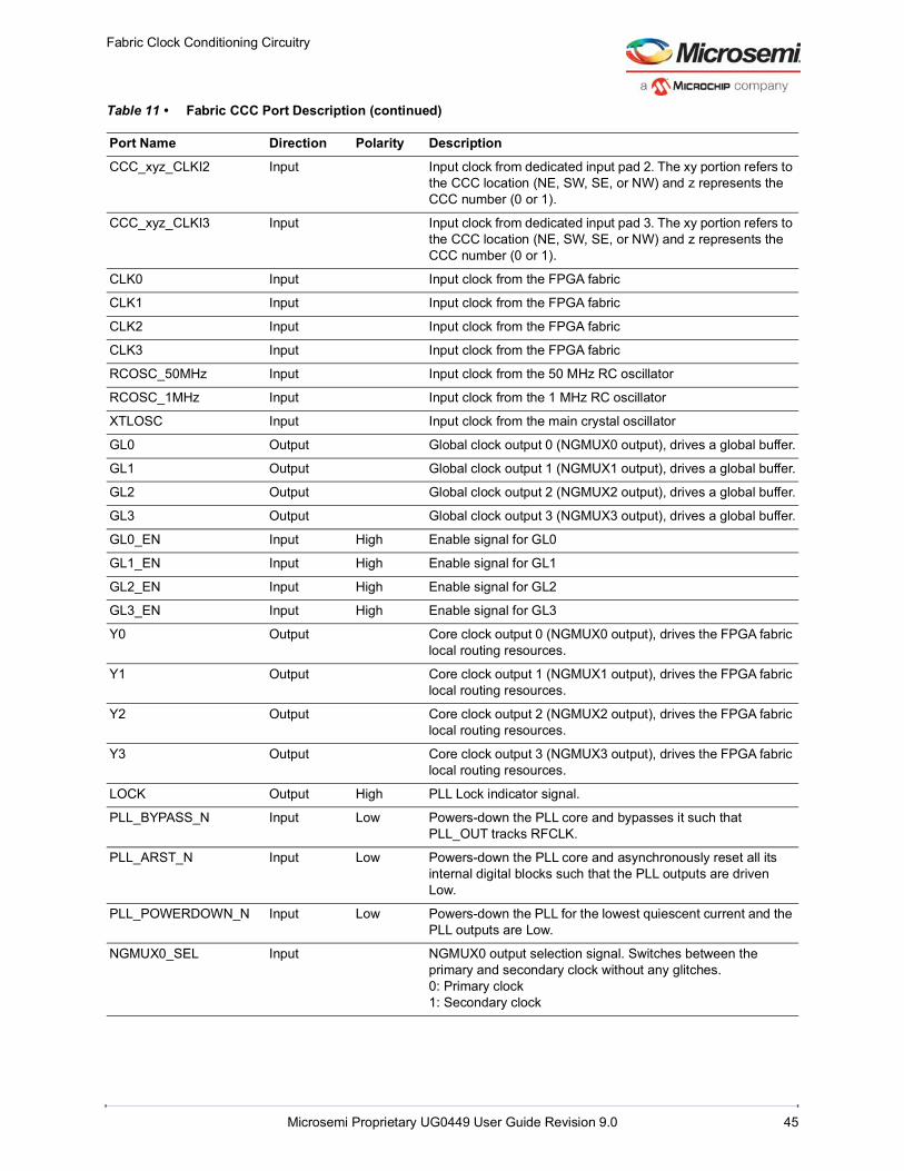
Fabric Clock Conditioning Circuitry
Microsemi Proprietary UG0449 User Guide Revision 9.0 45
CCC_xyz_CLKI2 Input Input clock from dedicated input pad 2. The xy portion refers to the CCC location (NE, SW, SE, or NW) and z represents the CCC number (0 or 1).
CCC_xyz_CLKI3 Input Input clock from dedicated input pad 3. The xy portion refers to the CCC location (NE, SW, SE, or NW) and z represents the CCC number (0 or 1).
CLK0 Input Input clock from the FPGA fabric
CLK1 Input Input clock from the FPGA fabric
CLK2 Input Input clock from the FPGA fabric
CLK3 Input Input clock from the FPGA fabric
RCOSC_50MHz Input Input clock from the 50 MHz RC oscillator
RCOSC_1MHz Input Input clock from the 1 MHz RC oscillator
XTLOSC Input Input clock from the main crystal oscillator
GL0 Output Global clock output 0 (NGMUX0 output), drives a global buffer.
GL1 Output Global clock output 1 (NGMUX1 output), drives a global buffer.
GL2 Output Global clock output 2 (NGMUX2 output), drives a global buffer.
GL3 Output Global clock output 3 (NGMUX3 output), drives a global buffer.
GL0_EN Input High Enable signal for GL0
GL1_EN Input High Enable signal for GL1
GL2_EN Input High Enable signal for GL2
GL3_EN Input High Enable signal for GL3
Y0 Output Core clock output 0 (NGMUX0 output), drives the FPGA fabric local routing resources.
Y1 Output Core clock output 1 (NGMUX1 output), drives the FPGA fabric local routing resources.
Y2 Output Core clock output 2 (NGMUX2 output), drives the FPGA fabric local routing resources.
Y3 Output Core clock output 3 (NGMUX3 output), drives the FPGA fabric local routing resources.
LOCK Output High PLL Lock indicator signal.
PLL_BYPASS_N Input Low Powers-down the PLL core and bypasses it such that PLL_OUT tracks RFCLK.
PLL_ARST_N Input Low Powers-down the PLL core and asynchronously reset all its internal digital blocks such that the PLL outputs are driven Low.
PLL_POWERDOWN_N Input Low Powers-down the PLL for the lowest quiescent current and the PLL outputs are Low.
NGMUX0_SEL Input NGMUX0 output selection signal. Switches between the primary and secondary clock without any glitches.0: Primary clock1: Secondary clock
Table 11 • Fabric CCC Port Description (continued)
Port Name Direction Polarity Description

Fabric Clock Conditioning Circuitry
Microsemi Proprietary UG0449 User Guide Revision 9.0 46
NGMUX1_SEL Input NGMUX1 output selection signal. Switches between the primary and secondary clock without any glitches.0: Primary clock1: Secondary clock
NGMUX2_SEL Input NGMUX2 output selection signal. Switches between the primary and secondary clock without any glitches.0: Primary clock1: Secondary clock
NGMUX3_SEL Input NGMUX3 output selection signal. Switches between the primary and secondary clock without any glitches.0: Primary clock1: Secondary clock
NGMUX0_HOLD_N Input Low NGMUX0 hold signal. Synchronously sets the NGMUX0 output low when 0.
NGMUX1_HOLD_N Input Low NGMUX1 hold signal. Synchronously sets the NGMUX1 output low when 0.
NGMUX2_HOLD_N Input Low NGMUX2 hold signal. Synchronously sets the NGMUX2 output low when 0.
NGMUX3_HOLD_N Input Low NGMUX3 hold signal. Synchronously sets the NGMUX3 output low when 0.
NGMUX0_ARST_N Input Low NGMUX0 asynchronous reset signal. Resets the NGMUX0 when 0.
NGMUX1_ARST_N Input Low NGMUX1 asynchronous reset signal. Resets the NGMUX1 when 0.
NGMUX2_ARST_N Input Low NGMUX2 asynchronous reset signal. Resets the NGMUX2 when 0.
NGMUX3_ARST_N Input Low NGMUX3 asynchronous reset signal. Resets the NGMUX3 when 0.
GPD0_ARST_N Input Low GPD0 asynchronous reset signal. The GPD0 is held in reset when 0.
GPD1_ARST_N Input Low GPD1 asynchronous reset signal. The GPD1 is held in reset when 0.
GPD2_ARST_N Input Low GPD2 asynchronous reset signal. The GPD2 is held in reset when 0.
GPD3_ARST_N Input Low GPD3 asynchronous reset signal. The GPD3 is held in reset when 0.
Fabric CCC Configuration Bus Interface Signals – APB3 Bus InterfacePCLK Input APB3 interface clock signal.
PRESET_N Input Low APB3 interface active low reset signal.
PADDR[7:2] Input APB3 interface address bus. This port is used to address fabric CCC internal registers.
PSEL Input APB3 interface slave select signal.
PENABLE Input APB3 interface strobe signal to indicate the second cycle of an APB3 transfer.
Table 11 • Fabric CCC Port Description (continued)
Port Name Direction Polarity Description

Fabric Clock Conditioning Circuitry
Microsemi Proprietary UG0449 User Guide Revision 9.0 47
5.4.1 Fabric CCC Output ClocksEach fabric CCC generates up to four different global clocks (GL0, GL1, GL2, and GL3) and four core clocks (Y0, Y1, Y2, and Y3) with a maximum frequency up to 400 MHz. The generated global clocks drive the FPGA fabric global networks and core clocks drive the local routing resources in the FPGA fabric. Fabric CCC's core clock outputs (Yx) can be used to drive internal logic without using the global network resources and introduce additional delay because of FPGA fabric routing. Core clocks are useful when global network resources must be conserved and utilized for other timing-critical paths. When using core clocks, timing analysis must be performed to ensure that there are no skew issues on these paths. The frequencies and phases of the core clocks are the same as those of the associated global clocks. The global buffers associated with the global clock outputs (GLx) are available to the user logic when the global clock outputs are not enabled. The fabric CCCs can be connected to each other or cascaded through the FPGA fabric.
Each of the four output clocks (GLx/Yx) can be driven by the following sources:
• PLL outputs• General purpose dividers (GPDs) outputs• Dedicated global I/Os• On-chip oscillators• FPGA fabric internal clock signals
5.4.2 Fabric CCC Clock SourcesThe following clock sources can be used to drive the fabric CCC clock input as well as the fabric CCC outputs (GLx/Yx) directly:
• 1 MHz RC Oscillator• 50 MHz RC Oscillator• Main Crystal Oscillator • Dedicated Global I/Os• FPGA Fabric Clock SourcesThe input clock frequency range for the fabric CCCs depends on the PLL usage for the output clocks generation.
• When the PLL is used, the PLL reference clock frequency must be between 1 MHz and 200 MHz.• CCC-NE1 has 32 KHz reference clock support.
• When the PLL is bypassed, the fabric CCC input clock frequency can be up to 400 MHz.
5.4.2.1 On-Chip OscillatorsOn-chip oscillators (1 MHz RC oscillator, 50 MHz RC oscillator, and main crystal oscillator) have direct access to the fabric CCC(s) through hardwired connections. To use a particular on-chip oscillator as a clock source, the Chip Oscillators macro must be instantiated in the design and its output connected to the associated fabric CCC input.
5.4.2.2 Dedicated Global I/OsThe dedicated global I/Os are the primary source for bringing external clock inputs into the SmartFusion2 or IGLOO2 device. Some of the dedicated global I/Os have direct access to the GBs, whereas others have to go through either fabric CCC or VCCC to reach GBs.
PWRITE Input APB3 interface read/write control signal. When High, this signal indicates an APB3 write access and when Low, a read access.
PWDATA[7:0] Input APB3 interface write data bus.
PRDATA[7:0] Output APB3 interface read data bus.
Table 11 • Fabric CCC Port Description (continued)
Port Name Direction Polarity Description

Fabric Clock Conditioning Circuitry
Microsemi Proprietary UG0449 User Guide Revision 9.0 48
Each fabric CCC has four dedicated global I/Os (CCC_xyz_CLKIw, w = 0 to 3) as inputs. These dedicated global I/Os have direct access to the fabric CCCs and are not routed through the FPGA fabric. Each fabric CCC output (GLx/Yx), as well as the PLL reference clock, can be driven from any one of the four dedicated global I/Os. Table 12, page 48 lists the dedicated global I/Os associated with each fabric CCC for the SmartFusion2 M2S050-FG896. As listed in the M2S050 FG896 Pin Function column of the table, some dedicated global I/Os are shared with the hard IP blocks such as MSS_MMUART, MSS_I2C, MSS_USB, MSS_GPIO, MDDR and FDDR. The shared dedicated global I/Os are not available to the fabric CCCs when the associated hard IP blocks are enabled and configured to use the shared dedicated global I/Os.
For other SmartFusion2 and IGLOO2 devices, see DS0115: SmartFusion2 Pin Descriptions Datasheet and DS0124: IGLOO2 Pin Descriptions Datasheet and the associated pin outs to identify the dedicated global I/Os associated with fabric CCCs.
See the Dedicated Global I/Os, page 12 for more information on dedicated global I/Os.
Table 12 • Dedicated Global I/Os Connections to the Fabric CCC/PLLs
CCC Location
Dedicated Global I/OPin Name
M2S050 FG896 Pin Number M2S050 FG896 Pin Function
CCC-NE1 CCC_NE1_CLKI0 V26 MSIO11NB3/I2C_1_SCL/GPIO_1_A/USB_DATA4_A
CCC_NE1_CLKI1 M25 MSIO40PB1/MMUART_1_RI/GPIO_15_B
CCC_NE1_CLKI2 A17 DDRIO76PB0/GB12/MDDR_DQ12
CCC_NE1_CLKI3 E17 DDRIO75PB0/MDDR_DQ14
CCC-NE0 CCC_NE0_CLKI0 V23 MSIO11PB3/I2C_1_SDA/GPIO_0_A/USB_DATA3_A
CCC_NE0_CLKI1 N23 MSIO39PB1/MMUART_1_CTS/GPIO_13_B
CCC_NE0_CLKI2 D15 DDRIO79PB0/MDDR_DQ10
CCC_NE0_CLKI3 A16 DDRIO78PB0/GB8/MDDR_DQS1
CCC-SW1 CCC_NW1_CLKI0 T7 MSIOD120PB7
CCC_NW1_CLKI1 R3 MSIOD118PB7/GB5
CCC_NW1_CLKI2 AG11 DDRIO152NB5/GB7/FDDR_DQ_ECC3
CCC_NW1_CLKI3 AK15 DDRIO159PB5/FDDR_DQ8
CCC-SW0 CCC_NW0_CLKI0 U7 MSIOD121PB7
CCC_NW0_CLKI1 R1 MSIOD119PB7/GB1
CCC_NW0_CLKI2 AG9 DDRIO147NB5
CCC_NW0_CLKI3 AF11 DDRIO152PB5/GB3/FDDR_DQ_ECC2
CCC-NW1 CCC_NW1_CLKI0 P9 MSIO116PB8
CCC_NW1_CLKI1 P3 MSIO114PB8/GB6
CCC_NW1_CLKI2 B9 DDRIO91NB0/GB4
CCC_NW1_CLKI3 E11 DDRIO87PB0/MDDR_DQ_ECC2
CCC-NW0 CCC_NW0_CLKI0 R9 MSIO117PB8
CCC_NW0_CLKI1 P1 MSIO115PB8/GB2
CCC_NW0_CLKI2 D9 DDRIO92NB0
CCC_NW0_CLKI3 A9 DDRIO91PB0/GB0

Fabric Clock Conditioning Circuitry
Microsemi Proprietary UG0449 User Guide Revision 9.0 49
5.4.2.3 FPGA Fabric Clock SourcesFPGA fabric clock sources are those clocks coming through FPGA fabric routed nets. Each fabric CCC has four clock inputs (CLKx, x = 0 to 3) from the FPGA fabric. Each fabric CCC output (GLx/Yx), as well as the reference clock, can be driven from any one of the four fabric clock inputs.
It is also possible to assign the fabric clock input to any of the regular I/O pins. Choosing this option provides the flexibility of selecting any regular I/O location but introduces additional delay due to FPGA fabric routing.
5.4.3 Fabric PLL CircuitryEach fabric CCC includes components for operating the PLL associated with it. Clocks requiring frequency synthesis and phase adjustments can utilize the PLL before connecting to the global or local routing networks. The following figure shows the block diagram of the fabric PLL circuitry. Fabric PLL circuitry includes the following components:
• PLL Core• RFMUX• FBMUX• RFDIV and FBDIV• RDLY and FBDLY
Figure 42 • Fabric PLL Circuitry
5.4.3.1 PLL CoreSmartFusion2 and IGLOO2 devices have two, six, or eight PLLs, depending on the size of the device (see Table 9, page 39). The PLL associated with the northeast corner fabric CCC (CCC-NE1), is capable of accepting 32 KHz reference clock input and generating an output frequency up to 1000 MHz. All other PLLs can accept a reference clock input ranging from 1 MHz to 200 MHz. The minimum output frequency of the PLL is 20 MHz. Each PLL includes a phase shifter and the PLL output clock is available in eight phases with a 45° phase difference (0°, 45°, 90°, 135°, 180°, 225°, 270°, and 315°). The VCO in the PLL Core has 500 MHz to 1000 MHz frequency range. The output divider (DIVQ) divides the VCO output frequency such that PLL generate frequencies in 20 MHz to 1000 MHz range. The PLL output is passed through GPD and it's division value must be configured such that the overall CCC output frequency must be less than or equal to 400 MHz. The following figure shows the PLL Core internal circuitry.
Figure 43 • PLL Core Internal Circuitry
PLL CoreRDLYRFDIV
FBDLYFBDIV
PLL_ARST_N
PLL_BYPASS_N
PLL_POWERDOWN_N
RFMUX
FBMUX
RFCLK
FBCLK
PLL_LOCK
PLL_OUT_0PLL_OUT_45PLL_OUT_90PLL_OUT_135
PLL_OUT_225PLL_OUT_270PLL_OUT_315
PLL_OUT_180
LOCKGeneration
CCC internal feedback
RCOSC_25_50MHzRCOSC_1MHz
XTLOSCCCC_xyz_CLKIw
CLKx 44
DIVQ[2:0]
DIVF[7:0]
DIVR[5:0]
SSCG PLL
RFCLK
FBCLKPLL_OUT[7:0]
PLL_LOCK
8
PLL Internal Feedback
VCO_OUT
PLL Core

Fabric Clock Conditioning Circuitry
Microsemi Proprietary UG0449 User Guide Revision 9.0 50
The fabric PLL features are configured using static flash bits set by the CCC macro available in the Libero SoC design software. The Libero SoC place-and-route software automatically uses the 32 KHz PLL when the PLL reference frequency is set to 32 KHz in the CCC macro configurator.
The supplies required to power the PLL are VDD for the digital section and an analog supply (CCC_xyz_PLL_VDDA, where xyz represents the CCC location and number) for the analog section. Each fabric PLL has its own analog supply pin. To achieve a reasonable level of long term jitter performance, it is vital to deliver a low noise power supply to the PLL. Typically an R-C or R-L-C filter is used, with the C being composed of multiple devices to achieve a wide spectrum of noise absorption. See DS0115: SmartFusion2 Pin Descriptions datasheet and DS0124: IGLOO2 Pin Descriptions datasheet for more information on the analog power supply pins of PLLs. The PLL analog supply voltage (CCC_xyz_PLL_VDDA) can be either 2.5 V or 3.3 V, based on the power supply availability on the board. User can only use either 3.3 V or 2.5 V PLL supply for the entire design. Libero does not support using both 2.5 V and 3.3 V power supplies for the PLLs used in a design. The analog power supply does not impact the PLL output frequency range. The PLL analog supply voltage is internally regulated, which provides independence from the external supply. See DS0128: SmartFusion2 and IGLOO2 Datasheet for the PLL operational range and characteristics.
Note: The unused PLLs are configured to be held in power-down mode so that they consume lowest quiescent current.
Note: If REFCK (Reference clock) is disconnected from the PLL then the VCO keeps running at a low-end frequency. If FBCK (Feedback clock) is disconnected from the PLL when in use then the VCO keeps running at a high-end frequency.
5.4.3.2 RFMUXAs shown in Figure 42, page 49, the reference clock multiplexer (RFMUX) allows selecting the PLL reference clock from the available fabric CCC clock sources.
5.4.3.3 FBMUXAs shown in Figure 42, page 49, the feedback clock multiplexer (FBMUX) allows selecting the PLL feedback clock source from an internal or an external feedback loop, depending on the system requirements. The internal feedback loop can be PLL internal feedback (not shown in Figure 42, page 49 because it is internal to the PLL core) or CCC internal feedback. The external feedback loop is from one of the CCC global clocks (GLx) through the FPGA fabric or externally to the chip through dedicated global I/O pads.
Minimum jitter and phase error can be achieved, if the PLL internal feedback loop is used. It is necessary to operate the PLL with internal feedback when its reference clock is set to 32 KHz. When PLL internal feedback is used, the programmable delay and GPD synchronization are not available.
The RFMUX and FBMUX have a feature to invert the clock inputs. Since the PLL aligns reference and feedback clocks on the rising clock edge, the inversion feature allows aligning them on the falling reference and feedback clocks.
5.4.3.4 RFDIV and FBDIVThe PLL reference clock divider (RFDIV) is an 8-bit programmable divider. The feedback clock divider (FBDIV) is a 14-bit programmable frequency divider. RFDIV and FBDIV generate PLL reference clock (RFCLK) and feedback clock (FBCLK). The function of RFDIV and FBDIV is described in the following equations:
RFCLK = (Input clock frequency) / (RFDIV [7:0] + 1)FBCLK = (Input clock frequency) / (FBDIV [13:0] + 1)
The visual CCC macro configurator derives the necessary divider values based on the input frequency, desired output frequencies, and the selected feedback loop. These dividers are configured statically by flash bits when the FPGA fabric is programmed.

Fabric Clock Conditioning Circuitry
Microsemi Proprietary UG0449 User Guide Revision 9.0 51
5.4.3.5 RDLY and FBDLY As shown in Figure 42, page 49, each fabric CCC has a programmable delay element in the PLL reference clock path (RDLY) and feedback loop path (FBDLY). For PLLs, adding delay in the reference clock path enables clock delay and adding delay in the feedback clock path enables clock advancement with respect to the PLL reference clock. A typical application for clock advancement is to advance the on-chip clock in order to cancel the global network delay and align the internal clock to an external clock on the board.
Each fabric CCC can be configured with a delay in the reference path or feedback path. The delay time of the programmable delay elements can be varied between 0 and 6.3 ns with a 100 ps step size. The programmable delay elements are bypassed when the PLL delay is set to zero or the PLL internal feedback loop is used.
5.4.3.6 Lock Generation CircuitA lock signal, PLL_LOCK, is provided to indicate that the PLL has locked onto the incoming signal. The lock signal asserts High to indicate that the frequency and phase lock is achieved. The precision of the lock discrimination can be adjusted using the lock window controls.
The lock window represents the phase error window for lock assertion as a fraction of the divided reference clock period. The lock window can be adjusted between 500 parts per million (ppm) and 64,000 ppm in powers of 2. The integration of the lock period can be adjusted using the lock counter. The lock counter or lock delay indicates the number of divided reference clock cycles to wait after the PLL is locked before asserting the lock signal. The lock delay is useful for avoiding false toggling of the lock signal. The lock counter can be configured between 32 and 10,48,576 cycles in multiples of 2.
For SmartFusion2 and IGLOO2 devices, if the fabric PLL reference clock is sourced from an internal RC oscillator, the minimum PLL lock window setting should be 64000 ppm and 32000 ppm for 1 MHz RC oscillator and 50 MHz RC oscillator, respectively. If the RFDIV divisor value is 2 or less and a wrong PLL lock window setting is used, then the PLL lock may get toggled.
Note: The combination of high register utilization and toggling rate results high PLL jitter and subsequently the PLL may come out of lock. Use higher PLL lock window for stable PLL operation.
5.4.3.7 Fabric PLL Control SignalsA reset control signal, PLL_ARST_N, is provided to power-down the PLL core and asynchronously reset all its internal digital blocks. When the PLL_ARST_N signal is asserted Low, all the PLL outputs are driven Low. A bypass signal, PLL_BYPASS_N, is provided which powers-down the PLL core and bypasses it such that the PLL output tracks the reference clock. All the output clocks have the same phase in PLL Bypass mode. The PLL_BYPASS_N signal has precedence over the PLL_ARST_N signal.
A fabric PLL can be held in Power-down mode for the lowest quiescent current by asserting its power-down control signal, PLL_POWERDOWN_N. When the PLL_POWERDOWN_N signal is asserted Low, the PLL powers-down and its outputs are held Low. The PLL_POWERDOWN_N signal has precedence over all other control signals. The following table shows the control signal values for PLL output and power states. Each PLL has its own control signals available to drive from the user logic in the FPGA fabric.
Table 13 • Control Signals for PLL Output and Power State
PLL_POWERDOWN_N PLL_BYPASS_N PLL_ARST_N PLL_OUT PLL POWER0 X X Low OFF
1 0 0 Low OFF
1 0 1 Tracks RFCLK input OFF
1 1 0 Low OFF
1 1 1 Normal Operation ON

Fabric Clock Conditioning Circuitry
Microsemi Proprietary UG0449 User Guide Revision 9.0 52
5.4.3.8 SSCGEach fabric PLL is integrated with a spread spectrum clock function for SSCG. The spread spectrum clocking feature spreads the fundamental clock signal energy to a wide band of frequencies to reduce the EMI.
As shown in the following figure, the spread spectrum function generates a down-spreading triangular modulation profile. The spread spectrum programmable options allow to control the modulation frequency and depth.
The modulation depth is represented by percentage spread which defines the frequency range of the modulated clock resulting from the spread spectrum modulation. For instance, with a down-spread percentage of 1.5% and nominal PLL output frequency of 100 MHz, the spread spectrum modulated output frequency is swept between 98.5 MHz and 100 MHz. See DS0128: SmartFusion2 and IGLOO2 FPGA Datasheet for the spread spectrum modulation characteristics of the fabric PLL.
The SSCG functionality is disabled if the down-spread percentage is set to 0%. More reduction in EMI can be achieved by spreading the clock energy over a wide band of frequencies. The modulation frequency is the rate at which the spreading signal sweeps from the minimum to the maximum PLL output frequency.
Note: The spread spectrum functionality of the PLL cannot be used with the 32 KHz reference clock input or when external PLL feedback input is used.
Figure 44 • Spread Spectrum Modulation
5.4.4 GPMUXThe clock source for generating the output clocks through GPDs is selected using a general purpose multiplexer (GPMUX). The output of the GPMUX is the clock input to the GPD. Each GPD has its own GPMUX that allows to choose the clock source independently for each GPD. Each GPMUX selects the clock source from the fabric CCC clock sources or PLL outputs, as shown in the following figure. The fabric PLL is bypassed if none of the fabric CCC outputs uses PLL outputs.
Each GPMUX has a feature to invert the output of the GPMUX that can be controlled by writing to appropriate fabric CCC configuration registers (FCCC_GPMUXx_CR, x = 0 to 3) through APB3 interface. See the Fabric CCC Configuration, page 58 for more information.
Figure 45 • GPMUX Input Clock Sources
Modulation Frequency
Modulation Depth
FmaxF
t
Output Clock (SSC)Output Clock (Non-SSC)
F : Output Frequencyt : Time
Fmax : Maximum Clock Frequency
Fmin
Fmin : Minimum Clock Frequency
GPMUX
CCC_xyz_CLKIw
PLL_OUT_x
CLKx
RCOSC_50MHz
RCOSC_1MHz
XTLOSC
SEL_GPMUX_X[4:0]
CLKIN
4
4
8

Fabric Clock Conditioning Circuitry
Microsemi Proprietary UG0449 User Guide Revision 9.0 53
5.4.5 GPDGPDs divide the frequency of the source clock selected by the GPMUX by a factor of 1 to 255 to generate the desired fabric CCC output frequencies as shown in the following equations. Each fabric CCC has four GPDs. The output of the GPDs can be used as the source for any of the four fabric CCC outputs. For instance, GPD0 can be used on a path to the GL1 output. The CCC macro configurator configures the GPD values to achieve the closest possible match to the desired output frequencies, based on the input frequency and the selected feedback loop.
CLKOUT = CLKIN / GPDx_DIV[7:0], for GPDx_DIV[7:0] = 1 TO 255
CLKOUT = CLKIN, for GPDx_DIV[7:0] = 0
The following figure shows a block diagram for a GPD block.
Figure 46 • GPD Block Diagram
The GPD’s behavior is outlined as follows:
• The duty cycle of the GPD output clock (CLKOUT) will be 50% if the duty cycle of the input clock (CLKIN) is 50%.
• The rising edge of CLKOUT always occurs as a result of a rising edge inputs on CLKIN.• The falling edge of CLKOUT always occurs as a result of a rising edge on CLKIN, if the divider value
is an even number > 2.• The falling edge of CLKOUT always occurs as a result of a falling edge on CLKIN, if the divider value
is an odd number or if divisor = 0 or 1.The GPDs divide the phase of the non-zero phase PLL output by the division value. In other words, the actual phase shift is not the same as the PLL phase shift selected, if the GPD division value is not one. The actual output phase shift of the output is shown in the fabric CCC configurator. For more information See the Output Clock Phase Adjustment, page 77.
Actual Phase Shift = (Selected PLL output phase shift) / (GPD division value)
As shown in Figure 46, page 53, each GPD has an asynchronous reset (GPD_ARST_N) and a synchronous reset (GPD_SYNCRST_N) for resetting the GPD. Both the resets are active Low. The GPD output clock (CLKOUT) is reset to Low when a reset signal is asserted. The asynchronous reset comes from the FPGA fabric and synchronous reset comes from the synchronous reset generator (SRG).
5.4.5.1 SRGThe SRG block sends synchronous reset signals to the GPDs when the PLL locks or on request by the System Controller. The purpose of the SRG is to synchronize (or re-align) the outputs of the GPDs with the PLL input clock after the PLL lock is achieved. This block also produces a LOCK signal which is sent out to the FPGA fabric.
The SRG has an internal reset pipeline stage to get the correct phase alignment at the GPD output while using non-zero phase PLL output as the GPD input. The CCC macro configurator automatically sets the reset pipeline stage control signal based on the GPD input selection.
GPD
SRG
CLKIN
CLKOUTGPDx_DIV[7:0]
GPD_SYNCRST_N
GPDx_ARST_NNOPIPE_RSTSYNCx
PLL_OUT_0
PLL_LOCKFBCLK
Configuration bits
LOCK

Fabric Clock Conditioning Circuitry
Microsemi Proprietary UG0449 User Guide Revision 9.0 54
Whenever GPD_SYNCRST_N changes from High to Low:
• CLKOUT is reset to Low at the next rising edge of CLKIN, if the internal reset pipeline stage is not enabled.
• CLKOUT is reset to Low at the second rising edge of CLKIN, if the internal reset pipeline stage is enabled.
The following figure shows the GPD output clock behavior for synchronous reset assertion.
Figure 47 • Assertion of GPD Synchronous Reset – GPD_SYNCRST_N
When releasing GPD_SYNCRST_N from Low to High:
• CLKOUT will be clocked to High at the next rising edge of CLKIN, if the reset pipeline stage is not enabled
• CLKOUT will be clocked to High at the second rising edge of CLKIN, if the internal reset pipeline stage is enabled.
The following figure shows the GPD output clock behavior for synchronous reset release.
Figure 48 • Releasing of GPD Synchronous Reset – GPD_SYNCRST_N
5.4.5.2 GPD Operating ModesThe GPDs support the following operating modes. For the GPDs that are driven by the PLL output clock, Microsemi recommends using either the first or second mode described below:
1. GPDs are held in reset after power-up, release and synchronize with the PLL reference clock after the PLL is locked:• If enabled, GPDs outputs are held in reset Low after power-up. Hence, the output(s) (GLx/Yx)
driven by the GPDs are held Low (or High if inverted) after power-up.• After the PLL lock is achieved, GPD's synchronous reset is released synchronously with second
FBCLK rising edge.• This mode can only be used if GPDs are not on the PLL external feedback path.• This mode is not available when the PLL internal feedback path is enabled.
GPD_SYNCRST_N
CLKOUT(divisor=3,NOPIPE_RSTSYNC=1)
CLKOUT(divisor=3,NOPIPE_RSTSYNC=0)
CLKIN
GPD_SYNCRST_N
CLKOUT(divisor=2,NOPIPE_RSTSYNC=1)
CLKOUT(divisor=2,NOPIPE_RSTSYNC=0)
CLKIN

Fabric Clock Conditioning Circuitry
Microsemi Proprietary UG0449 User Guide Revision 9.0 55
The following figure shows the GPDs outputs (CLKOUT1 and CLKOUT2) synchronization operation for this mode.
• The PLL source clock goes to PLL through RFDIV and the RFDIV division value is set to 4 (divided by 5)
• The FBDIV division value is set to 4 (divided by 5)• CLKOUT1 is generated by a GPD whose input is PLL_OUT_0 and the GPD divider value is set to 3• CLKOU T2 is generated by another GPD whose input is PLL_OUT_270 and the GPD divider value
is set to 5.Figure 49 • GPD_SYNCRST_N Released after PLL Locks
2. GPDs operate after power-up and resynchronize with the PLL reference clock after the PLL is locked:• If enabled, GPDs operate after power-up. Hence, the outputs (GLx/Yx) driven by the GPDs are
operational after power-up.• When the PLL is locked and detected by the rising edge of PLL_OUT_0, the SRG asserts the
GPD_SYNCRST_N signal after completion of one PLL_OUT_0 clock cycle.• After GPD_SYNCRST_N is asserted, the SRG waits for the first rising edge of FBCLK to trigger
the counting of (M – 1) clock edges of PLL_OUT_0 clock, where M = FBDIV [13:0] + 1.• The SRG releases GPD_SYNCRST_N on the (M – 1)th rising edge of PLL_OUT_0 clock to let
GPD start counting on the Mth clock edge of PLL_OUT_0 clock. In other words, the release of GPD_SYNCRST_N restarts the GPDs on the PLL output clock edge, which correspond to the 2nd rising edge of FBCLK after the lock changes state from 0 to 1.
• This mode can only be used if GPDs are not on the PLL external feedback path.• This mode is not available when the PLL internal feedback path is enabled.
CKOUT is CLK[0] divided by 3,CKOUT2 is CLK[6] divided by 5FIN is CLK[0] divided by 5 (= FBDIV )
PLL Source Clock
FBCLK
PLL_LOCK
GPD_SYNCRST_N
LOCK
CLKOUT1
CLKOUT2
PLL_OUT_0
PLL_OUT_45
PLL_OUT_135
PLL_OUT_90
PLL_OUT_180
PLL_OUT_225
PLL_OUT_270
PLL_OUT_315
PLL locks hereGPD_SYNCRST_N
is deasserted
CLKOUT2 is derived from PLL_OUT_270, so the pipeline stagein GPD is enabled,and will start tocount from here
CLKOUT1 is derived from PLL_OUT_0, sothe pipeline stagein GPD is disabled, and will start to count from here
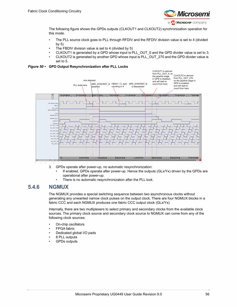
Fabric Clock Conditioning Circuitry
Microsemi Proprietary UG0449 User Guide Revision 9.0 56
The following figure shows the GPDs outputs (CLKOUT1 and CLKOUT2) synchronization operation for this mode.
• The PLL source clock goes to PLL through RFDIV and the RFDIV division value is set to 4 (divided by 5)
• The FBDIV division value is set to 4 (divided by 5)• CLKOUT1 is generated by a GPD whose input is PLL_OUT_0 and the GPD divider value is set to 3.• CLKOUT2 is generated by another GPD whose input is PLL_OUT_270 and the GPD divider value is
set to 5.Figure 50 • GPD Output Resynchronization after PLL Locks
3. GPDs operate after power-up, no automatic resynchronization:• If enabled, GPDs operate after power-up. Hence the outputs (GLx/Yx) driven by the GPDs are
operational after power-up.• There is no automatic resynchronization after the PLL lock.
5.4.6 NGMUXThe NGMUX provides a special switching sequence between two asynchronous clocks without generating any unwanted narrow clock pulses on the output clock. There are four NGMUX blocks in a fabric CCC and each NGMUX produces one fabric CCC output clock (GLx/Yx).
Internally, there are two multiplexers to select primary and secondary clocks from the available clock sources. The primary clock source and secondary clock source to NGMUX can come from any of the following clock sources:
• On-chip oscillators• FPGA fabric• Dedicated global I/O pads• 8 PLL outputs• GPDs outputs
G3 style sync reset generation, on LOCK
The circuit is operated by CLK[0], the dividers which receive CLK[0] as input do not require a pipeline stag
receive CLK[1:7] as input will need a pipeline stage for SYNCB. Therefore a pipeline stage exists in the general purpose divider, which is
enabled by a flash bit.
CLKOUT is CLK[0] divided by 3,CLKOUT2 is CLK[6] divided by 5FIN is CLK[0] divided by 5 (= FBDIV )
FBDIV = 4, startcounting to 4
GPD_SYNCRST_N is deasserted
CLKOUT1 is derivedfrom PLL_OUT_0, sothe pipeline stage in GPD is disabled, and will start to count from here
CLKOUT2 is derived from PLL_OUT_270, so the pipeline stage inGPD is enabled,and will start tocount from here
PLL locks here
lock detected
GPD_SYNCRST_Nasserted
PLL Source Clock
FBCLK
PLL_LOCKGPD_SYNCRST_N
(internal_sig_1)
(internal_sig_2)
CLKOUT1
CLKOUT2
PLL_OUT_0
PLL_OUT_45
PLL_OUT_135
PLL_OUT_90
PLL_OUT_180
PLL_OUT_225
PLL_OUT_270
PLL_OUT_315
LOCK

Fabric Clock Conditioning Circuitry
Microsemi Proprietary UG0449 User Guide Revision 9.0 57
The following figure shows the NGMUX circuit.
Figure 51 • NGMUX Circuit
The resulting two internal clocks (primary and secondary) are fed to an NGMUX that allows switching between the two clocks without any glitches. The selection control input for each NGMUX (NGMUX_SEL) comes from the fabric logic and can be changed dynamically. The NGMUX is bypassed when there is no secondary clock source.
Each NGMUX has an asynchronous active low reset signal (NGMUX_ARST_N) to force the NGMUX output to Low. Asserting the NGMUX_ARST_N may cause a narrow pulse on the NGMUX output, so this must only be used for system reset on power-up or to clear an error condition. During run-time, use NGMUX_HOLD_N control input, if it is required to hold the NGMUX output at Low. The NGMUX_ARST_N and NGMUX_SEL signals are to be managed as follows for a glitch-less transition of clocks using NGMUX. After device power-up, reset using NGMUX_ARST_N signal to ensure that the NGMUX is in safe state. Then trigger a switch using NGMUX_SEL signal when both clock sources are stable and ready.
5.4.6.1 Clock SwitchingThe sequence of clock switching between the primary clock (CLK1) and the secondary clock (CLK2) is explained in this section. The clock switching specified here is for the selection change from the primary clock to the secondary clock, and the same rule applies when selection changes from the secondary clock to the primary clock.
Upon changing the selection control input (NGMUX_SEL), the NGMUX output (GLx/Yx) follows the original clock waveform for "1 fall and then 4 rise-and-fall" sequence, as shown in the following figure. Then the NGMUX output is grounded and waits for the "1 fall and then 4 rise-and-fall" sequence of the new clock, after which the NGMUX output is driven by the new clock. After the transition is done, the original clock can be stopped. The maximum frequency of the primary and secondary clocks is 400 MHz.
Figure 52 • Clock Switching Using NGMUX
PrimaryClock
SecondaryClock
NGMUX
MUX_CLK1
MUX_CLK2
CLKIN
NGMUX_SEL
NGMUX_ARST_N
NGMUX_HOLD_N
GLx/Yx
23
0
1
0
1
sel[9:5]
sel[4:0]
selout
OUT_MUX
NGMUX_SEL
CLK2
CLK1
GLx/Yx

Fabric Clock Conditioning Circuitry
Microsemi Proprietary UG0449 User Guide Revision 9.0 58
The primary clock and secondary clock source must generate free-running clocks without any glitches for glitch free clock switching. If not, the NGMUX may still produce unwanted glitches on the output clock.
The requirements for a successful clock switching are:
1. The primary and second clocks must be toggled during the switching operation.2. NGMUX_SEL signal must not be switched when the previous switch is still under-going and not yet
completed.The output of the NGMUX is undefined if NGMUX_SEL changes when the previous switch is still in progress. For any clock switching between CLK1 and CLK2 with a relationship other than as described above, the output clock is not guaranteed to be glitch free and it may fail to switch between clock sources. The asynchronous reset, NGMUX_ARST_N, can be used to provide reset if such a condition occurs.
It is possible to read the state of the NGMUX through APB3 configuration bus. The FCCC_NGMUXx_CR1[NGMUXx_BUSY] register field indicates the NGMUX switching status. When NGMUXx_BUSY is '1', the switching is in progress, old clock source must keep toggling until this signal becomes low and no new switching must be started.
5.4.6.2 Clock HoldingEach NGMUX has its own control input (NGMUX_HOLD_N) from the FPGA fabric to hold the clock output at Low. When the NGMUX_HOLD_N control signal is asserted, both corresponding Y and GL outputs will be synchronously set to low. During run-time, the NGMUX_HOLD_N control input can be driven to stop/start the clock without any glitches. The NGMUX_HOLD_N control input has precedence over the NGMUX_SEL. Once the NGMUX_HOLD_N signal is deasserted, the NGMUX synchronously switches to one of the two input clocks based on the NGMUX_SEL value.
5.4.6.3 Clock InversionEach NGMUX can be configured to invert the polarity of output clock from its source. If the NGMUX inversion feature is enabled, both the primary and secondary clocks are inverted.
5.4.7 Clock GatingThe global clocks (GLx) generated from the fabric CCCs can be gated dynamically by driving the control signals (GLx_EN, where x ranges from 0 to 3) from the FPGA fabric. See the Clock Gating, page 20 of FPGA Fabric Global Network Architecture chapter for more information. See Figure 36, page 40 and Figure 37, page 40 for more information on the clocking hierarchy.
5.5 Fabric CCC ConfigurationFabric CCC(s) are configurable statically through flash configuration bits set in the programming bitstream or dynamically through an APB3 bus interface. The flash configuration bits are the configuration bits associated with programmed flash switches. The fabric CCC flash configuration bits provide the default operating state of the fabric CCC.
5.5.1 Fabric CCC Static ConfigurationThe CCC macro available in the IP Catalog of the Libero SoC design software provides a visual configuration wizard for a quick and easy way to configure the fabric CCC with desired the settings.
5.5.2 Fabric CCC Dynamic ConfigurationEach fabric CCC has an APB3 bus interface for dynamic configuration of the fabric CCC parameters without reprogramming the device. The fabric CCC configuration is controlled by volatile configuration registers which are loaded with values from the flash configuration bits at power-up. An APB3 master can change the fabric CCC configuration by writing to the appropriate registers. See the Fabric CCC Configuration Registers, page 59 for more information on fabric CCC control registers and their bit definitions.
To meet all the datasheet specifications, there are certain requirements that must be met when configuring the PLL parameters. The Libero CCC configurator implements all these requirements and creates a valid solution for the requested output clock frequencies and phases. Hence, it is
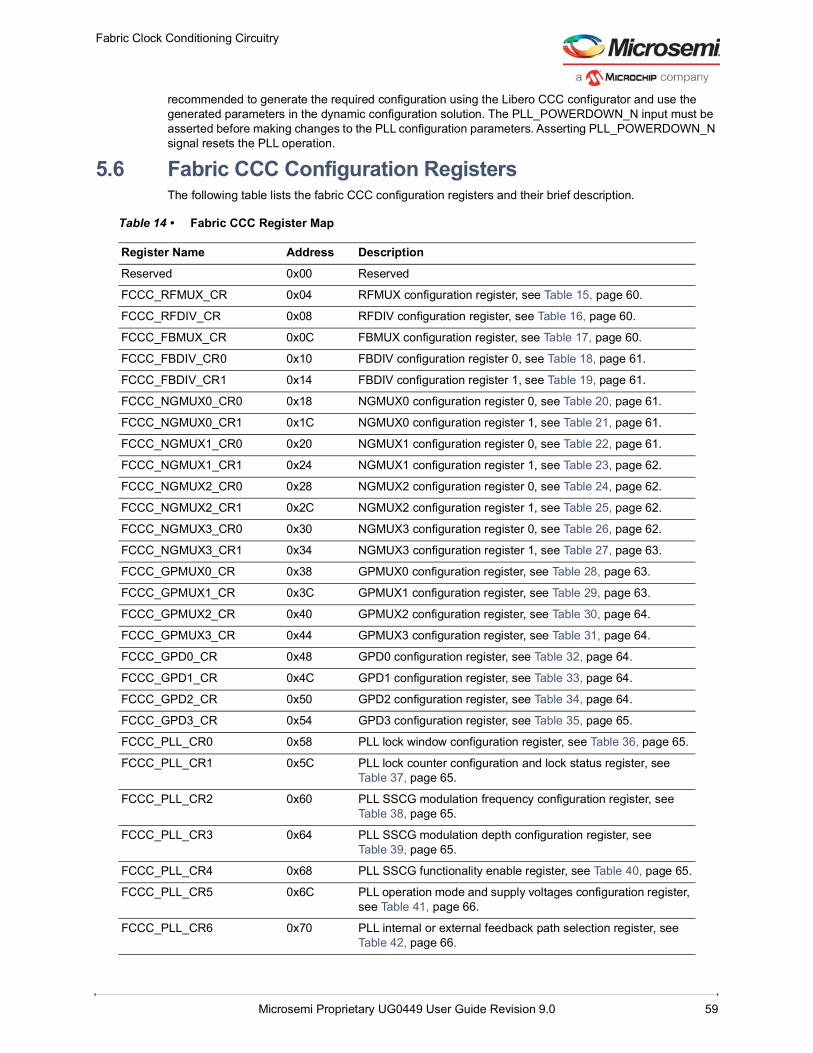
Fabric Clock Conditioning Circuitry
Microsemi Proprietary UG0449 User Guide Revision 9.0 59
recommended to generate the required configuration using the Libero CCC configurator and use the generated parameters in the dynamic configuration solution. The PLL_POWERDOWN_N input must be asserted before making changes to the PLL configuration parameters. Asserting PLL_POWERDOWN_N signal resets the PLL operation.
5.6 Fabric CCC Configuration RegistersThe following table lists the fabric CCC configuration registers and their brief description.
Table 14 • Fabric CCC Register Map
Register Name Address DescriptionReserved 0x00 Reserved
FCCC_RFMUX_CR 0x04 RFMUX configuration register, see Table 15, page 60.
FCCC_RFDIV_CR 0x08 RFDIV configuration register, see Table 16, page 60.
FCCC_FBMUX_CR 0x0C FBMUX configuration register, see Table 17, page 60.
FCCC_FBDIV_CR0 0x10 FBDIV configuration register 0, see Table 18, page 61.
FCCC_FBDIV_CR1 0x14 FBDIV configuration register 1, see Table 19, page 61.
FCCC_NGMUX0_CR0 0x18 NGMUX0 configuration register 0, see Table 20, page 61.
FCCC_NGMUX0_CR1 0x1C NGMUX0 configuration register 1, see Table 21, page 61.
FCCC_NGMUX1_CR0 0x20 NGMUX1 configuration register 0, see Table 22, page 61.
FCCC_NGMUX1_CR1 0x24 NGMUX1 configuration register 1, see Table 23, page 62.
FCCC_NGMUX2_CR0 0x28 NGMUX2 configuration register 0, see Table 24, page 62.
FCCC_NGMUX2_CR1 0x2C NGMUX2 configuration register 1, see Table 25, page 62.
FCCC_NGMUX3_CR0 0x30 NGMUX3 configuration register 0, see Table 26, page 62.
FCCC_NGMUX3_CR1 0x34 NGMUX3 configuration register 1, see Table 27, page 63.
FCCC_GPMUX0_CR 0x38 GPMUX0 configuration register, see Table 28, page 63.
FCCC_GPMUX1_CR 0x3C GPMUX1 configuration register, see Table 29, page 63.
FCCC_GPMUX2_CR 0x40 GPMUX2 configuration register, see Table 30, page 64.
FCCC_GPMUX3_CR 0x44 GPMUX3 configuration register, see Table 31, page 64.
FCCC_GPD0_CR 0x48 GPD0 configuration register, see Table 32, page 64.
FCCC_GPD1_CR 0x4C GPD1 configuration register, see Table 33, page 64.
FCCC_GPD2_CR 0x50 GPD2 configuration register, see Table 34, page 64.
FCCC_GPD3_CR 0x54 GPD3 configuration register, see Table 35, page 65.
FCCC_PLL_CR0 0x58 PLL lock window configuration register, see Table 36, page 65.
FCCC_PLL_CR1 0x5C PLL lock counter configuration and lock status register, see Table 37, page 65.
FCCC_PLL_CR2 0x60 PLL SSCG modulation frequency configuration register, see Table 38, page 65.
FCCC_PLL_CR3 0x64 PLL SSCG modulation depth configuration register, see Table 39, page 65.
FCCC_PLL_CR4 0x68 PLL SSCG functionality enable register, see Table 40, page 65.
FCCC_PLL_CR5 0x6C PLL operation mode and supply voltages configuration register, see Table 41, page 66.
FCCC_PLL_CR6 0x70 PLL internal or external feedback path selection register, see Table 42, page 66.
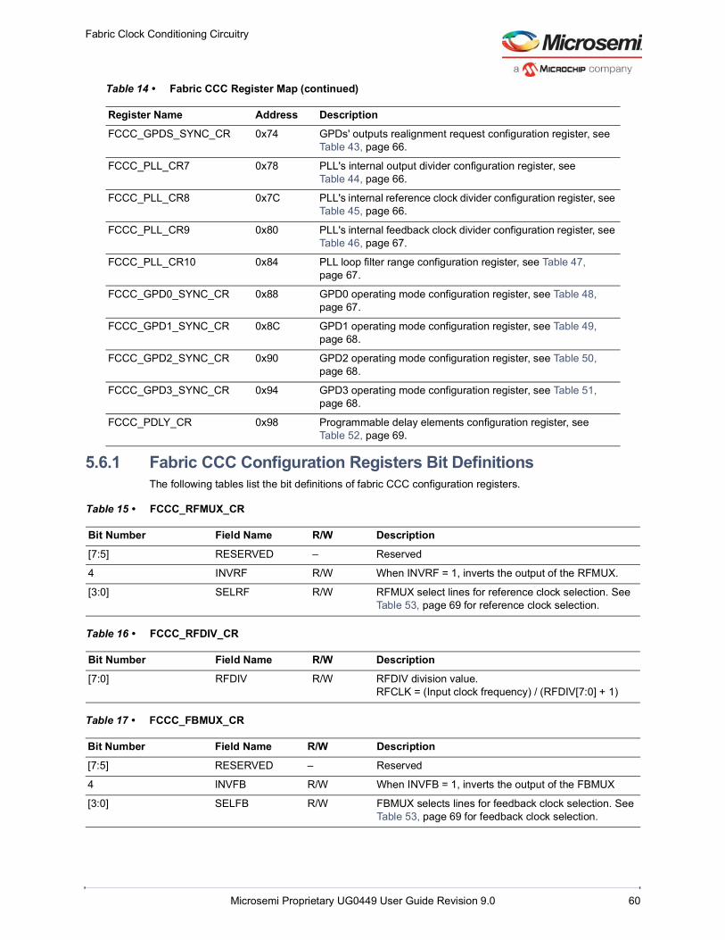
Fabric Clock Conditioning Circuitry
Microsemi Proprietary UG0449 User Guide Revision 9.0 60
5.6.1 Fabric CCC Configuration Registers Bit Definitions The following tables list the bit definitions of fabric CCC configuration registers.
FCCC_GPDS_SYNC_CR 0x74 GPDs' outputs realignment request configuration register, see Table 43, page 66.
FCCC_PLL_CR7 0x78 PLL's internal output divider configuration register, see Table 44, page 66.
FCCC_PLL_CR8 0x7C PLL's internal reference clock divider configuration register, see Table 45, page 66.
FCCC_PLL_CR9 0x80 PLL's internal feedback clock divider configuration register, see Table 46, page 67.
FCCC_PLL_CR10 0x84 PLL loop filter range configuration register, see Table 47, page 67.
FCCC_GPD0_SYNC_CR 0x88 GPD0 operating mode configuration register, see Table 48, page 67.
FCCC_GPD1_SYNC_CR 0x8C GPD1 operating mode configuration register, see Table 49, page 68.
FCCC_GPD2_SYNC_CR 0x90 GPD2 operating mode configuration register, see Table 50, page 68.
FCCC_GPD3_SYNC_CR 0x94 GPD3 operating mode configuration register, see Table 51, page 68.
FCCC_PDLY_CR 0x98 Programmable delay elements configuration register, see Table 52, page 69.
Table 15 • FCCC_RFMUX_CR
Bit Number Field Name R/W Description[7:5] RESERVED – Reserved
4 INVRF R/W When INVRF = 1, inverts the output of the RFMUX.
[3:0] SELRF R/W RFMUX select lines for reference clock selection. See Table 53, page 69 for reference clock selection.
Table 16 • FCCC_RFDIV_CR
Bit Number Field Name R/W Description[7:0] RFDIV R/W RFDIV division value.
RFCLK = (Input clock frequency) / (RFDIV[7:0] + 1)
Table 17 • FCCC_FBMUX_CR
Bit Number Field Name R/W Description[7:5] RESERVED – Reserved
4 INVFB R/W When INVFB = 1, inverts the output of the FBMUX
[3:0] SELFB R/W FBMUX selects lines for feedback clock selection. See Table 53, page 69 for feedback clock selection.
Table 14 • Fabric CCC Register Map (continued)
Register Name Address Description

Fabric Clock Conditioning Circuitry
Microsemi Proprietary UG0449 User Guide Revision 9.0 61
Table 18 • FCCC_FBDIV_CR0
Bit Number Field Name R/W Description[7:0] FBDIV[7:0] R/W FBDIV division value - 8 LSBs
FBCLK = (Input clock frequency) / (FBDIV[13:0] + 1)
Table 19 • FCCC_FBDIV_CR1
Bit Number Field Name R/W Description[7:6] RESERVED – Reserved
[5:0] FBDIV[13:8] R/W FBDIV division value - 6 MSBsFBCLK = (Input clock frequency) / (FBDIV[13:0] + 1)
Table 20 • FCCC_NGMUX0_CR0
Bit Number Field Name R/W Description[7:5] RESERVED – Reserved
[4:0] SELGL[4:0] R/W NGMUX0 primary clock source selection. NGMUX0 primary clock is the output of NGMUX0_CLK1 multiplexer. See Table 53, page 69 for primary clock source selection.
Table 21 • FCCC_NGMUX0_CR1
Bit Number Field Name R/W Description7 NGMUX0_BUSY R NGMUX0 status. The reset value is '0'.
1: Switching is in progress, old clock source should keep toggling until this signal becomes low and no new switching should be started0: Switching is not in progress
6 SELOUT_0 R/W Select or bypass NGMUX01: NGMUX0 is used0: NGMUX0 is bypassed
5 INVGL_0 R/W NGMUX0 output inversion1: Invert the NGMUX0 output0: Non-inverted NGMUX0 output
[4:0] SELGL[9:5] R/W NGMUX0 secondary clock source selection.NGMUX0 secondary clock is the output of NGMUX0_CLK2 multiplexer. See Table 53, page 69 for secondary clock source selection.
Table 22 • FCCC_NGMUX1_CR0
Bit Number Field Name R/W Description[7:5] RESERVED – Reserved
[4:0] SELGL[14:10] R/W NGMUX1 primary clock source selection.NGMUX1 primary clock is the output of NGMUX1_CLK1 multiplexer. See Table 53, page 69 for primary clock source selection.
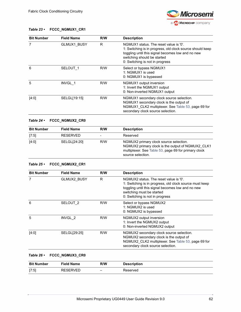
Fabric Clock Conditioning Circuitry
Microsemi Proprietary UG0449 User Guide Revision 9.0 62
Table 23 • FCCC_NGMUX1_CR1
Bit Number Field Name R/W Description7 GLMUX1_BUSY R NGMUX1 status. The reset value is '0'.
1: Switching is in progress, old clock source should keep toggling until this signal becomes low and no new switching should be started0: Switching is not in progress
6 SELOUT_1 R/W Select or bypass NGMUX11: NGMUX1 is used0: NGMUX1 is bypassed
5 INVGL_1 R/W NGMUX1 output inversion1: Invert the NGMUX1 output0: Non-inverted NGMUX1 output
[4:0] SELGL[19:15] R/W NGMUX1 secondary clock source selection.NGMUX1 secondary clock is the output of NGMUX1_CLK2 multiplexer. See Table 53, page 69 for secondary clock source selection.
Table 24 • FCCC_NGMUX2_CR0
Bit Number Field Name R/W Description[7:5] RESERVED - Reserved
[4:0] SELGL[24:20] R/W NGMUX2 primary clock source selection.NGMUX2 primary clock is the output of NGMUX2_CLK1 multiplexer. See Table 53, page 69 for primary clock source selection.
Table 25 • FCCC_NGMUX2_CR1
Bit Number Field Name R/W Description7 GLMUX2_BUSY R NGMUX2 status. The reset value is '0'.
1: Switching is in progress, old clock source must keep toggling until this signal becomes low and no new switching must be started0: Switching is not in progress
6 SELOUT_2 R/W Select or bypass NGMUX21: NGMUX2 is used0: NGMUX2 is bypassed
5 INVGL_2 R/W NGMUX2 output inversion1: Invert the NGMUX2 output0: Non-inverted NGMUX2 output
[4:0] SELGL[29:25] R/W NGMUX2 secondary clock source selection.NGMUX2 secondary clock is the output of NGMUX2_CLK2 multiplexer. See Table 53, page 69 for secondary clock source selection.
Table 26 • FCCC_NGMUX3_CR0
Bit Number Field Name R/W Description[7:5] RESERVED – Reserved

Fabric Clock Conditioning Circuitry
Microsemi Proprietary UG0449 User Guide Revision 9.0 63
[4:0] SELGL[34:30] R/W NGMUX3 primary clock source selection.NGMUX3 primary clock is the output of NGMUX3_CLK1 multiplexer. See Table 53, page 69 for primary clock source selection.
Table 27 • FCCC_NGMUX3_CR1
Bit Number Field Name R/W Description7 GLMUX3_BUSY R NGMUX3 status. The reset value is '0'.
1: Switching is in progress, old clock source must keep toggling until this signal becomes low and no new switching must be started0: Switching is not in progress
6 SELOUT_3 R/W Select or bypass NGMUX31: NGMUX3 is used0: NGMUX3 is bypassed
5 INVGL_3 R/W NGMUX3 output inversion1: Invert the NGMUX3 output0: Non-inverted NGMUX3 output
[4:0] SELGL[39:35] R/W NGMUX3 secondary clock source selectionNGMUX3 secondary clock is the output of NGMUX3_CLK2 multiplexer. See Table 53, page 69 for secondary clock source selection.
Table 28 • FCCC_GPMUX0_CR
Bit Number Field Name R/W Description7 RESERVED – Reserved
6 NOPIPE_SYNCRST0 R/W 1: Disable pipe-line stage for GPD0 synchronous reset is disabled0: Enable pipe-line stage
5 INV_GPMUX0 R/W 1: Invert the output of the GPMUX00: Disable the clock inversion of GPMUX0The default value of this bit is 0.
[4:0] SEL_GPMUX0 R/W Select lines for the GPMUX0. See Table 53, page 69 for GPMUX0 output selection.
Table 29 • FCCC_GPMUX1_CR
Bit Number Field Name R/W Description7 RESERVED – Reserved
6 NOPIPE_SYNCRST1 R/W 1: Disable pipe-line stage for GPD1 synchronous reset is disabled0: Enable pipe-line stage
5 INV_GPMUX1 R/W 1: Invert the output of the GPMUX10: Disable the clock inversion of GPMUX1The default value of this bit is 0.
[4:0] SEL_GPMUX1 R/W Select lines for the GPMUX1. See Table 53, page 69 for GPMUX1 output selection.
Table 26 • FCCC_NGMUX3_CR0
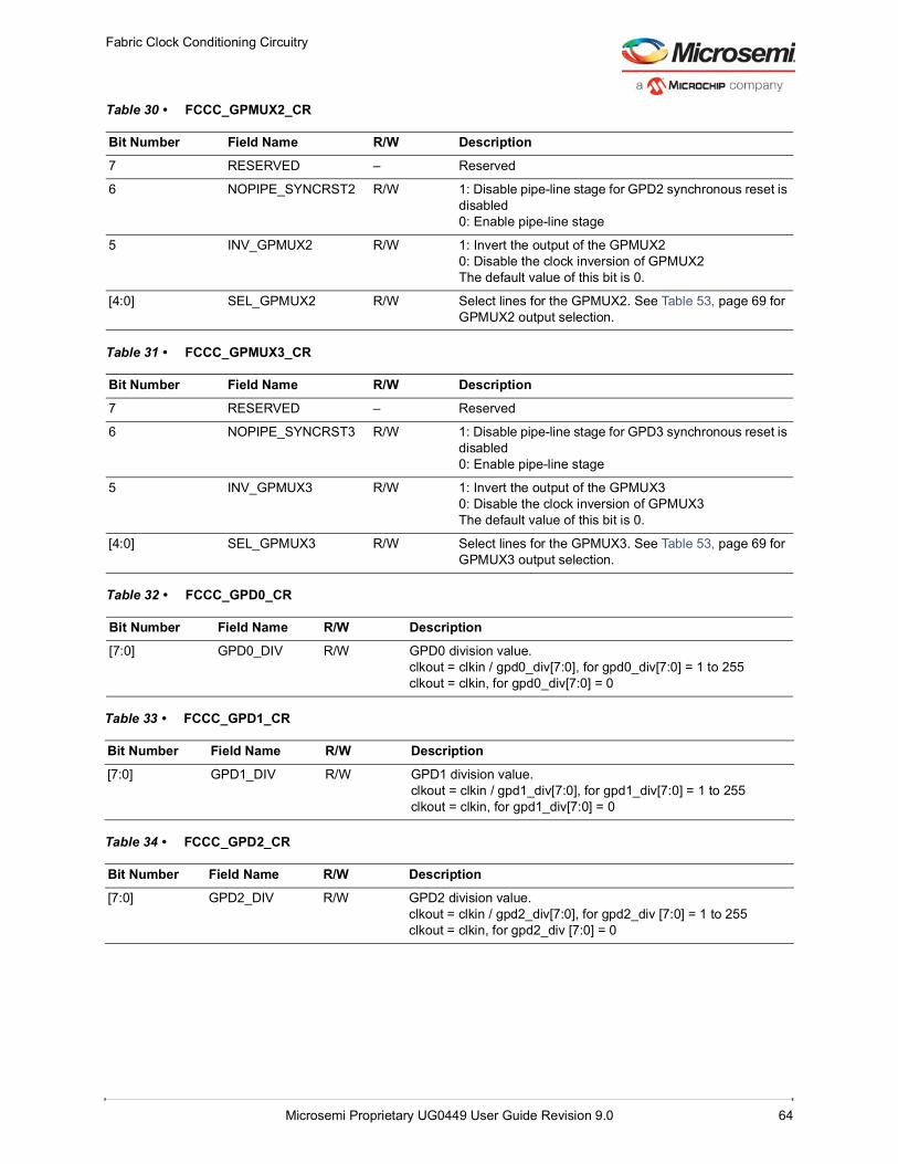
Fabric Clock Conditioning Circuitry
Microsemi Proprietary UG0449 User Guide Revision 9.0 64
Table 30 • FCCC_GPMUX2_CR
Bit Number Field Name R/W Description7 RESERVED – Reserved
6 NOPIPE_SYNCRST2 R/W 1: Disable pipe-line stage for GPD2 synchronous reset is disabled0: Enable pipe-line stage
5 INV_GPMUX2 R/W 1: Invert the output of the GPMUX20: Disable the clock inversion of GPMUX2The default value of this bit is 0.
[4:0] SEL_GPMUX2 R/W Select lines for the GPMUX2. See Table 53, page 69 for GPMUX2 output selection.
Table 31 • FCCC_GPMUX3_CR
Bit Number Field Name R/W Description7 RESERVED – Reserved
6 NOPIPE_SYNCRST3 R/W 1: Disable pipe-line stage for GPD3 synchronous reset is disabled0: Enable pipe-line stage
5 INV_GPMUX3 R/W 1: Invert the output of the GPMUX30: Disable the clock inversion of GPMUX3The default value of this bit is 0.
[4:0] SEL_GPMUX3 R/W Select lines for the GPMUX3. See Table 53, page 69 for GPMUX3 output selection.
Table 32 • FCCC_GPD0_CR
Bit Number Field Name R/W Description[7:0] GPD0_DIV R/W GPD0 division value.
clkout = clkin / gpd0_div[7:0], for gpd0_div[7:0] = 1 to 255clkout = clkin, for gpd0_div[7:0] = 0
Table 33 • FCCC_GPD1_CR
Bit Number Field Name R/W Description[7:0] GPD1_DIV R/W GPD1 division value.
clkout = clkin / gpd1_div[7:0], for gpd1_div[7:0] = 1 to 255clkout = clkin, for gpd1_div[7:0] = 0
Table 34 • FCCC_GPD2_CR
Bit Number Field Name R/W Description[7:0] GPD2_DIV R/W GPD2 division value.
clkout = clkin / gpd2_div[7:0], for gpd2_div [7:0] = 1 to 255clkout = clkin, for gpd2_div [7:0] = 0
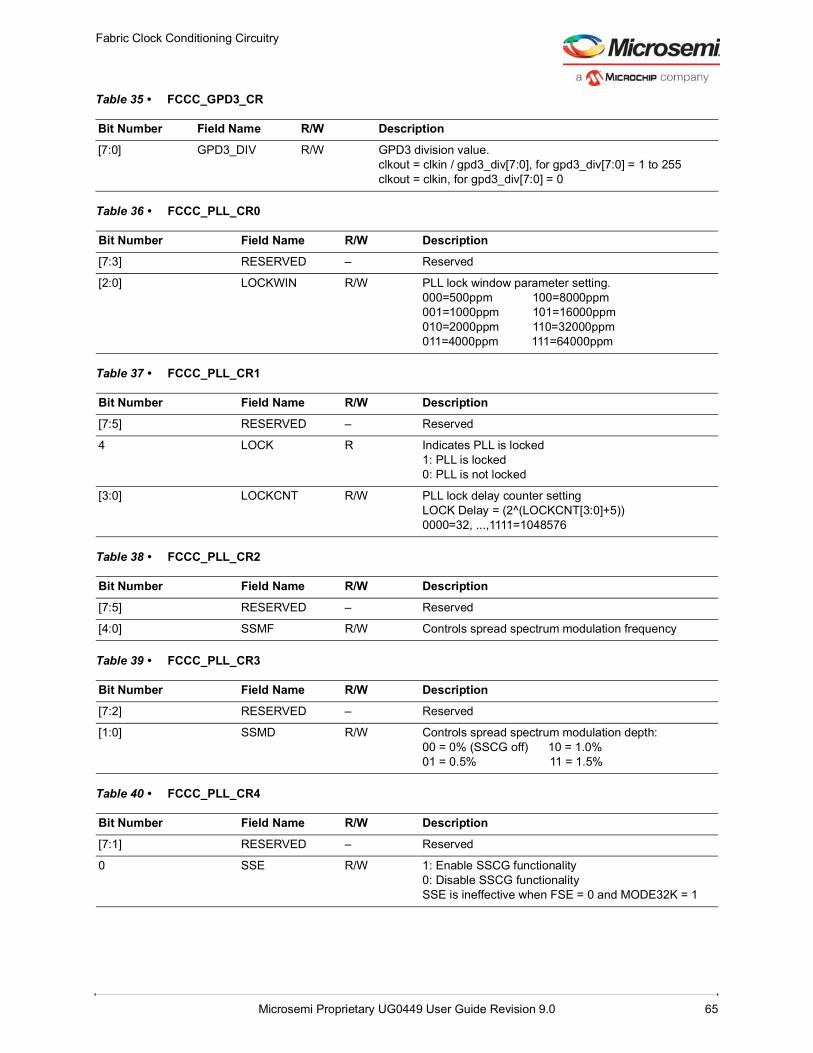
Fabric Clock Conditioning Circuitry
Microsemi Proprietary UG0449 User Guide Revision 9.0 65
Table 35 • FCCC_GPD3_CR
Bit Number Field Name R/W Description[7:0] GPD3_DIV R/W GPD3 division value.
clkout = clkin / gpd3_div[7:0], for gpd3_div[7:0] = 1 to 255clkout = clkin, for gpd3_div[7:0] = 0
Table 36 • FCCC_PLL_CR0
Bit Number Field Name R/W Description[7:3] RESERVED – Reserved
[2:0] LOCKWIN R/W PLL lock window parameter setting.000=500ppm 100=8000ppm 001=1000ppm 101=16000ppm010=2000ppm 110=32000ppm011=4000ppm 111=64000ppm
Table 37 • FCCC_PLL_CR1
Bit Number Field Name R/W Description[7:5] RESERVED – Reserved
4 LOCK R Indicates PLL is locked1: PLL is locked0: PLL is not locked
[3:0] LOCKCNT R/W PLL lock delay counter settingLOCK Delay = (2^(LOCKCNT[3:0]+5))0000=32, ...,1111=1048576
Table 38 • FCCC_PLL_CR2
Bit Number Field Name R/W Description[7:5] RESERVED – Reserved
[4:0] SSMF R/W Controls spread spectrum modulation frequency
Table 39 • FCCC_PLL_CR3
Bit Number Field Name R/W Description[7:2] RESERVED – Reserved
[1:0] SSMD R/W Controls spread spectrum modulation depth:00 = 0% (SSCG off) 10 = 1.0%01 = 0.5% 11 = 1.5%
Table 40 • FCCC_PLL_CR4
Bit Number Field Name R/W Description[7:1] RESERVED – Reserved
0 SSE R/W 1: Enable SSCG functionality0: Disable SSCG functionalitySSE is ineffective when FSE = 0 and MODE32K = 1

Fabric Clock Conditioning Circuitry
Microsemi Proprietary UG0449 User Guide Revision 9.0 66
Table 41 • FCCC_PLL_CR5
Bit Number Field Name R/W Description[7:3] RESERVED – Reserved
2 MODE_3V3 R/W PLL analog supply voltage selection1-3.3 V0-2.5 V
1 MODE_1V2 R/W PLL core supply voltage selection1-1.2 V 0-Not supported
0 MODE32K R/W Selects PLL 32 kHz operating mode1-32 KHz mode selected0-32 KHz mode is not active, input frequency range is 1 MHz to 200 MHz.
Table 42 • FCCC_PLL_CR6
Bit Number Field Name R/W Description[7:1] RESERVED – Reserved
0 FSE R/W Chooses between internal and external feedback 1: PLL internal feedback path selected0: External feedback path selected
Table 43 • FCCC_GPDS_SYNC_CR
Bit Number Field Name R/W Description[7:1] RESERVED – Reserved
0 SW_RESYNC_GPD
R/W To request realignment of GPDs' output. A pulse of 1 to 0 requests the realignment of GPDs' output, and then the GPDs is resynchronized by resetting.
Table 44 • FCCC_PLL_CR7
Bit Number Field Name R/W Description[7:3] RESERVED – Reserved
[2:0] DIVQ R/W PLL's internal output divider division value.Valid divider values are 1, 2, 4, 8, 16, and 32:000 = ÷1001 = ÷2010 = ÷4011 = ÷8100 = ÷16101 = ÷32
Table 45 • FCCC_PLL_CR8
Bit Number Field Name R/W Description[7:6] RESERVED – Reserved
[5:0] DIVR R/W PLL's internal reference divider division value.000000 = ÷1, …,111111 = ÷64
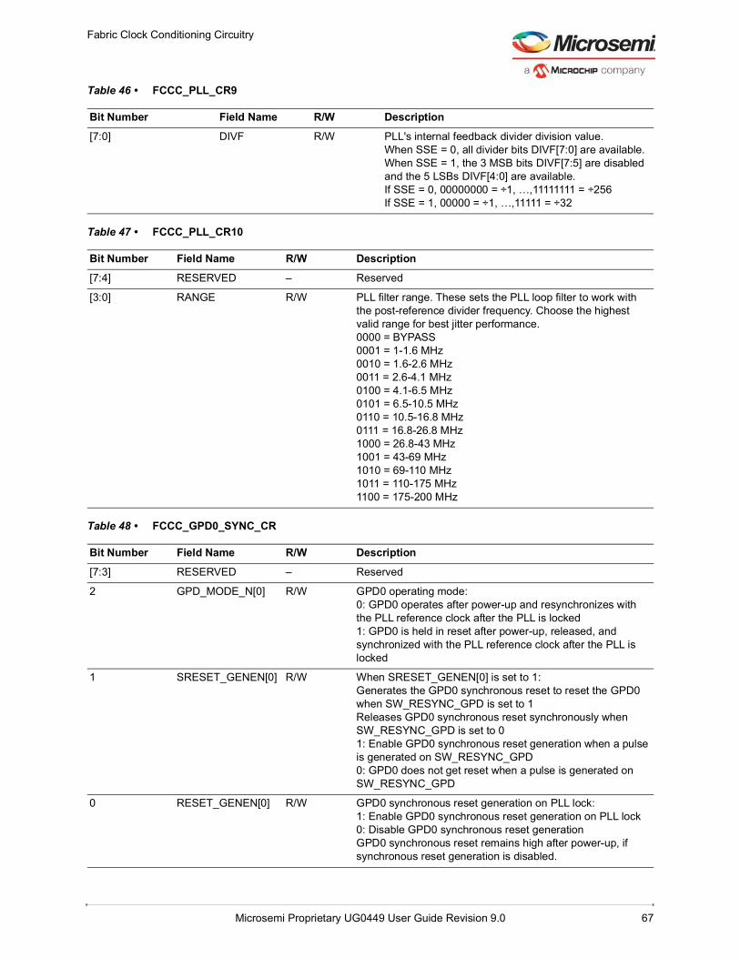
Fabric Clock Conditioning Circuitry
Microsemi Proprietary UG0449 User Guide Revision 9.0 67
Table 46 • FCCC_PLL_CR9
Bit Number Field Name R/W Description[7:0] DIVF R/W PLL's internal feedback divider division value.
When SSE = 0, all divider bits DIVF[7:0] are available.When SSE = 1, the 3 MSB bits DIVF[7:5] are disabled and the 5 LSBs DIVF[4:0] are available.If SSE = 0, 00000000 = ÷1, …,11111111 = ÷256If SSE = 1, 00000 = ÷1, …,11111 = ÷32
Table 47 • FCCC_PLL_CR10
Bit Number Field Name R/W Description[7:4] RESERVED – Reserved
[3:0] RANGE R/W PLL filter range. These sets the PLL loop filter to work with the post-reference divider frequency. Choose the highest valid range for best jitter performance. 0000 = BYPASS0001 = 1-1.6 MHz0010 = 1.6-2.6 MHz0011 = 2.6-4.1 MHz0100 = 4.1-6.5 MHz0101 = 6.5-10.5 MHz0110 = 10.5-16.8 MHz0111 = 16.8-26.8 MHz1000 = 26.8-43 MHz1001 = 43-69 MHz1010 = 69-110 MHz1011 = 110-175 MHz1100 = 175-200 MHz
Table 48 • FCCC_GPD0_SYNC_CR
Bit Number Field Name R/W Description[7:3] RESERVED – Reserved
2 GPD_MODE_N[0] R/W GPD0 operating mode:0: GPD0 operates after power-up and resynchronizes with the PLL reference clock after the PLL is locked1: GPD0 is held in reset after power-up, released, and synchronized with the PLL reference clock after the PLL is locked
1 SRESET_GENEN[0] R/W When SRESET_GENEN[0] is set to 1: Generates the GPD0 synchronous reset to reset the GPD0 when SW_RESYNC_GPD is set to 1Releases GPD0 synchronous reset synchronously when SW_RESYNC_GPD is set to 01: Enable GPD0 synchronous reset generation when a pulse is generated on SW_RESYNC_GPD0: GPD0 does not get reset when a pulse is generated on SW_RESYNC_GPD
0 RESET_GENEN[0] R/W GPD0 synchronous reset generation on PLL lock:1: Enable GPD0 synchronous reset generation on PLL lock0: Disable GPD0 synchronous reset generation GPD0 synchronous reset remains high after power-up, if synchronous reset generation is disabled.

Fabric Clock Conditioning Circuitry
Microsemi Proprietary UG0449 User Guide Revision 9.0 68
Table 49 • FCCC_GPD1_SYNC_CR
Bit Number Field Name R/W Description[7:3] RESERVED – Reserved
2 GPD_MODE_N[1] R/W GPD1 operating mode:0: GPD1 operates after power-up and resynchronizes with the PLL reference clock after the PLL is locked1: GPD1 is held in reset after power-up, released, and synchronized with the PLL reference clock after the PLL is locked
1 SRESET_GENEN[1] R/W When SRESET_GENEN[1] is set to 1: Generates the GPD1 synchronous reset to reset the GPD1 when SW_RESYNC_GPD is set to 1Releases GPD1 synchronous reset synchronously when SW_RESYNC_GPD is set to 01: Enable GPD1 synchronous reset generation when a pulse is generated on SW_RESYNC_GPD0: GPD1 does not reset when a pulse is generated on SW_RESYNC_GPD
0 RESET_GENEN[1] R/W GPD1 synchronous reset generation on PLL lock:1: Enable GPD1 synchronous reset generation on PLL lock0: Disable GPD1 synchronous reset generation GPD1 synchronous reset remains high after power-up, if synchronous reset generation is disabled.
Table 50 • FCCC_GPD2_SYNC_CR
Bit Number Field Name R/W Description[7:3] RESERVED – Reserved
2 GPD_MODE_N[2] R/W GPD2 operating mode:0: GPD2 operates after power-up and resynchronizes with the PLL reference clock after the PLL is locked1: GPD2 is held in reset after power-up, released, and synchronized with the PLL reference clock after the PLL is locked
1 SRESET_GENEN[2] R/W When SRESET_GENEN[2] is set to 1: Generates the GPD2 synchronous reset to reset the GPD2 when SW_RESYNC_GPD is set to 1Releases GPD2 synchronous reset synchronously when SW_RESYNC_GPD is set to 01: Enable GPD2 synchronous reset generation when a pulse is generated on SW_RESYNC_GPD0: GPD2 does not reset when a pulse is generated on SW_RESYNC_GPD
0 RESET_GENEN[2] R/W GPD2 synchronous reset generation on PLL lock:1: Enable GPD2 synchronous reset generation on PLL lock0: Disable GPD2 synchronous reset generation GPD2 synchronous reset remains high after power-up, if synchronous reset generation is disabled.
Table 51 • FCCC_GPD3_SYNC_CR
Bit Number Field Name R/W Description[7:3] RESERVED – Reserved

Fabric Clock Conditioning Circuitry
Microsemi Proprietary UG0449 User Guide Revision 9.0 69
2 GPD_MODE_N[3] R/W GPD3 operating mode:0: GPD3 operates after power-up and resynchronizes with the PLL reference clock after the PLL is locked1: GPD3 is held in reset after power-up, released, and synchronized with the PLL reference clock after the PLL is locked
1 SRESET_GENEN[3] R/W When SRESET_GENEN[3] is set to 1: • Generates the GPD3 synchronous reset to reset the
GPD3 when SW_RESYNC_GPD is set to 1• Releases GPD3 synchronous reset synchronously
when SW_RESYNC_GPD is set to 01: Enable GPD3 synchronous reset generation when a pulse is generated on SW_RESYNC_GPD0: GPD3 does not get reset when a pulse is generated on SW_RESYNC_GPD
0 RESET_GENEN[3] R/W GPD3 synchronous reset generation on PLL lock:1: Enable GPD3 synchronous reset generation on PLL lock0: Disable GPD3 synchronous reset generation GPD3 synchronous reset remains high after power-up, if synchronous reset generation is disabled.
Table 52 • FCCC_PDLY_CR
Bit Number Field Name R/W Description7 RESERVED – Reserved
6 RF_DLINE R/W If RF_DLINE = 1, delay setting SEL_PLL_DLINE[5:0] is applied to the delay line in the PLL reference clock path (RDLY). The setting for the feedback clock path delay line (FBDLY) is set to 0. This enables clock-delay.If RF_DLINE = 0, delay setting SEL_PLL_DLINE[5:0] is applied to the delay line in the PLL feedback clock path (FBDLY). The setting for the reference clock path delay line (RDLY) is set to 0. This enables clock-acceleration.
[5:0] SEL_PLL_DLINE R/W Programmable delay lines setting. If set to 6'b000000, the clock delay lines on both reference and feedback paths are bypassed.
Table 53 • Fabric CCC's Multiplexers Selection Control
MUX Selection Input RFMUX Output FBMUX Output
GPMUXx Output (x = 0 to 3)
NGMUXx_CLK1/NGMUXx_CLK2 Output (x = 0 to 3
0 CCC_xyz_CLKI0 CCC_xyz_CLKI0 PLL_OUT_315 PLL_OUT_315
1 CCC_xyz_CLKI1 CCC_xyz_CLKI1 PLL_OUT_270 PLL_OUT_270
2 CCC_xyz_CLKI2 CCC_xyz_CLKI2 PLL_OUT_225 PLL_OUT_225
3 CCC_xyz_CLKI3 CCC_xyz_CLKI3 PLL_OUT_180 PLL_OUT_180
4 Reserved Reserved PLL_OUT_135 PLL_OUT_135
5 Reserved Reserved PLL_OUT_90 PLL_OUT_90
6 Reserved Reserved PLL_OUT_45 PLL_OUT_45
Table 51 • FCCC_GPD3_SYNC_CR (continued)
Bit Number Field Name R/W Description

Fabric Clock Conditioning Circuitry
Microsemi Proprietary UG0449 User Guide Revision 9.0 70
5.7 How to Use Fabric CCC(s) The CCC macro configurator enables static configuration of the CCC/PLL blocks available in SmartFusion2 and IGLOO2 devices. The CCC macro must be instantiated into the design in order to use a fabric CCC. Multiple CCC macros must be instantiated in order to use more than one fabric CCC in a design. The CCC configurator includes the following tabs:
• Basic Configuration• Advanced Configuration• PLL Options
7 Reserved PLL_OUT_0 PLL_OUT_0 PLL_OUT_0
8 Logic - 0 Logic - 0 Reserved GPD0_CLKOUT
9 XTLOSC Reserved Reserved GPD1_CLKOUT
10 RCOSC_1MHz Reserved Reserved GPD2_CLKOUT
11 RCOSC_50MHz Reserved Reserved GPD3_CLKOUT
12 CLK0 CLK0 Reserved Reserved
13 CLK1 CLK1 Reserved Reserved
14 CLK2 CLK2 Reserved Reserved
15 CLK3 CLK3 Reserved Reserved
16 CCC_xyz_CLKI0 CCC_xyz_CLKI0
17 CCC_xyz_CLKI1 CCC_xyz_CLKI1
18 CCC_xyz_CLKI2 CCC_xyz_CLKI2
19 CCC_xyz_CLKI3 CCC_xyz_CLKI3
20 CLK0 CLK0
21 CLK1 CLK1
22 CLK2 CLK2
23 CLK3 CLK3
24 Logic - 0 Logic - 0
25 XTLOSC XTLOSC
26 RCOSC_1MHz RCOSC_1MHz
27 RCOSC_50MHz RCOSC_50MHz
28 Reserved Reserved
29 Reserved Reserved
30 Reserved Reserved
31 Reserved Reserved
Table 53 • Fabric CCC's Multiplexers Selection Control (continued)
MUX Selection Input RFMUX Output FBMUX Output
GPMUXx Output (x = 0 to 3)
NGMUXx_CLK1/NGMUXx_CLK2 Output (x = 0 to 3

Fabric Clock Conditioning Circuitry
Microsemi Proprietary UG0449 User Guide Revision 9.0 71
5.7.1 Basic ConfigurationThe following figure shows the CCC configurator Basic tab and highlights the configurable options.
Figure 53 • CCC Basic Configuration Tab
Microsemi recommends the following flow to configure clocks generated by the CCC for basic use cases. In the Basic tab, perform the following:
1. Select the number of desired output clocks (up to 4), as shown in the following figure.Figure 54 • CCC Output Selection

Fabric Clock Conditioning Circuitry
Microsemi Proprietary UG0449 User Guide Revision 9.0 72
2. For each selected output clock, set the desired output frequency as shown in the following figure. Actual output frequencies achieved by the CCC configurator are shown in the Actual column of the Basic tab.
Figure 55 • Set the Desired Output Frequency
3. Configure the CCC reference clock source and frequency, as shown in the following figure.Figure 56 • CCC Reference Clock Selection
In basic configuration, the PLL is always used to generate the output frequency. The feedback of the PLL is internal to the CCC.
Fabric Clock Conditioning Circuitry
Microsemi Proprietary UG0449 User Guide Revision 9.0 73
5.7.2 Advanced ConfigurationThe following figure shows the CCC configurator Advanced tab and highlights the configurable options.
Figure 57 • CCC Advanced Configuration Tab
For advanced use cases, Microsemi recommends to use the following flow to configure the clocks generated by the CCC (flow proceeds from right to left in the GUI, as shown in Figure 57, page 73):
• Select the number of desired output clocks (up to 4 global and local clocks).• For each selected output clock, set the desired output frequency.• For each selected output clock, select the desired reference clock (NGMUX primary clock) from
which the output will be derived. It can be either of the following:• One of the CCC input clocks (PLL Bypass mode)• One of the 8 PLL output phases
• If required, configure the NGMUX secondary clock frequency and reference clock from which it will be derived. It can be either of the following:• One of the CCC input clocks (PLL Bypass mode)• One of the 8 PLL output phases
• If PLL is used: • Select the PLL reference clock source and frequency.• Select the PLL feedback clock source.• Select the PLL analog supply voltage to either 2.5 V or 3.3 V to match the supply on the board• If required, enable the programmable delay elements by configuring the delay.
• Enter the frequency of each selected clock source(s). The configurator uses these frequencies to compute the division factor of the PLL reference and feedback dividers as well as the GPD dividers shown in blue on the GUI.
• Configure Advanced options, such as GPD output synchronization configuration, PLL SSCG, and LOCK control parameters in the PLL Options tab, as shown in the following figure.
Input Clock Selection
Feedback Clock Selection
Clock Sources
RFDIV and FBDIV settings
Programmable Delay Selection GPD setting
Primary Clock Selection
Secondary Clock Selection
Desired Primary Clock Frequency
Desired Secondary Clock Frequency
Local Output selection
Global Output selection
Clock Gating Selection

Fabric Clock Conditioning Circuitry
Microsemi Proprietary UG0449 User Guide Revision 9.0 74
The CCC configurator automatically tries to compute a configuration that meets the frequency requirements and all the internal CCC/PLL constraints. If the configurator is unable to find an exact solution for all requirements, it finds a configuration that globally minimizes the error between the required and actual frequency. Actual data (divider settings, PLL output frequency, and actual output frequencies) is shown in the Advanced tab in blue.
Figure 58 • CCC PLL Options Configuration Tab
The following subsections explain the advanced configuration options available in the Advanced tab of the CCC configurator. The flow proceeds from right (output) to left (input) in the Advanced tab of the CCC configurator.
PLL LOCK Window Configuration
PLL LOCK Delay Configuration
GDP Output Synchronization Configuration
PLL SSCG Configuration
Expose Fabric CCC Configuration Bus and Control Signals

Fabric Clock Conditioning Circuitry
Microsemi Proprietary UG0449 User Guide Revision 9.0 75
5.7.2.1 Gated Clock ConfigurationFor the selected global clock outputs (GLx), you can choose to have enable (GLx_EN) signal that can enable or disable the global clocks, as shown in the following figure.
Figure 59 • Clock Gating
5.7.2.2 Primary Clock Source SelectionThe source of the GLx/Yx clocks can be one of the CCC input clocks or the PLL outputs. You must specify the required primary output clock frequency, as shown in the following figure.
Figure 60 • Primary Clock Source and Output Frequency Selection

Fabric Clock Conditioning Circuitry
Microsemi Proprietary UG0449 User Guide Revision 9.0 76
5.7.2.3 Secondary Clock Source SelectionEach enabled clock output can be configured to use a secondary clock source. You must specify the required secondary output clock frequency. Selecting a secondary clock source enables the NGMUX and exposes the input signal NGMUXx_SEL (with x = 0, 1, 2, 3). This signal can be used to dynamically switch between the primary and secondary clock. The transitions from primary to secondary clock and secondary to primary clock are guaranteed to be glitch free.
The following figure shows how to specify the secondary clock source.
Figure 61 • Secondary Clock Source and Output Frequency Selection
5.7.2.4 Inversion ConfigurationEach clock output can be inverted if required, as shown in the following figure. The inversion affects both the primary and secondary clock.
Figure 62 • Clock Inversion Configuration
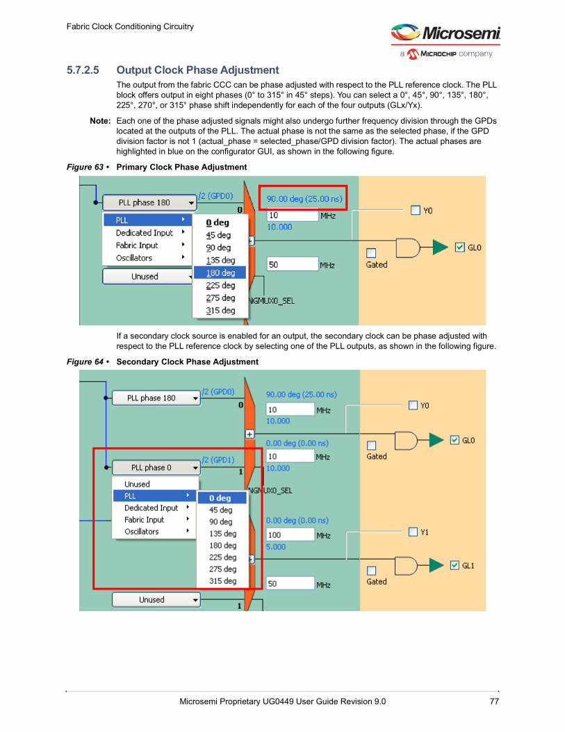
Fabric Clock Conditioning Circuitry
Microsemi Proprietary UG0449 User Guide Revision 9.0 77
5.7.2.5 Output Clock Phase AdjustmentThe output from the fabric CCC can be phase adjusted with respect to the PLL reference clock. The PLL block offers output in eight phases (0° to 315° in 45° steps). You can select a 0°, 45°, 90°, 135°, 180°, 225°, 270°, or 315° phase shift independently for each of the four outputs (GLx/Yx).
Note: Each one of the phase adjusted signals might also undergo further frequency division through the GPDs located at the outputs of the PLL. The actual phase is not the same as the selected phase, if the GPD division factor is not 1 (actual_phase = selected_phase/GPD division factor). The actual phases are highlighted in blue on the configurator GUI, as shown in the following figure.
Figure 63 • Primary Clock Phase Adjustment
If a secondary clock source is enabled for an output, the secondary clock can be phase adjusted with respect to the PLL reference clock by selecting one of the PLL outputs, as shown in the following figure.
Figure 64 • Secondary Clock Phase Adjustment

Fabric Clock Conditioning Circuitry
Microsemi Proprietary UG0449 User Guide Revision 9.0 78
5.7.2.6 PLL Reference Clock Source SelectionThe PLL reference clock source and feedback clock source must be configured if any of the PLL outputs are selected for generating the output clocks. The PLL is bypassed if the PLL outputs are not selected for any of the clock outputs. The PLL reference clock source can be selected from the available CCC input clock sources, as shown in the following figure.
Figure 65 • PLL Reference Clock Source Selection
5.7.2.7 Internal PLL Feedback Clock SourceAs shown in Figure 66, page 78, if you choose to use the PLL with internal feedback, the feedback path can be one of the following:
• CCC internal feedback from PLL phase 0° output – Default value (Figure 67, page 78)• PLL internal feedback from PLL phase 0° output – This is a shorter feedback path integrated within
the PLL (Figure 68, page 79). You must use PLL internal feedback when using spread spectrum modulation or if the PLL reference clock frequency is 32 KHz. Programmable delay and output synchronization are not available in this mode.
Figure 66 • Internal PLL Feedback Clock Source Selection
Figure 67 • CCC Internal Feedback
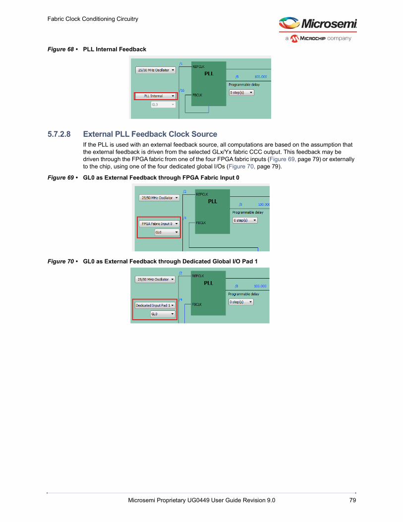
Fabric Clock Conditioning Circuitry
Microsemi Proprietary UG0449 User Guide Revision 9.0 79
Figure 68 • PLL Internal Feedback
5.7.2.8 External PLL Feedback Clock SourceIf the PLL is used with an external feedback source, all computations are based on the assumption that the external feedback is driven from the selected GLx/Yx fabric CCC output. This feedback may be driven through the FPGA fabric from one of the four FPGA fabric inputs (Figure 69, page 79) or externally to the chip, using one of the four dedicated global I/Os (Figure 70, page 79).
Figure 69 • GL0 as External Feedback through FPGA Fabric Input 0
Figure 70 • GL0 as External Feedback through Dedicated Global I/O Pad 1

Fabric Clock Conditioning Circuitry
Microsemi Proprietary UG0449 User Guide Revision 9.0 80
5.7.2.9 Clock Delay AdjustmentAs shown in the following figure, the programmable delay elements can be enabled for clock delay adjustments. The programmable delay has 64 positive steps when applied to the PLL reference clock path and 64 negative steps when applied to the PLL feedback clock. See DS0128: SmartFusion2 and IGLOO2 Datasheet or perform timing analysis for the actual value of each step. The programmable delay steps are not compensated for process, voltage, or temperature (PVT).
The programmable delay elements are not available when the PLL internal feedback path is selected.
Figure 71 • Programmable Delay Configuration
5.7.2.10 CCC Input Clock SourcesThe following sources are available as the CCC inputs for the PLL reference clock, PLL feedback clock, and output direct connection:
• Dedicated input pads: The clock source is one of the four dedicated global I/Os that has a dedicated path to the CCC. • Some of the dedicated inputs to the CCC can be configured to use a differential I/O technology.
• FPGA fabric inputs: The clock source can be any signal coming from the FPGA fabric. • Main crystal oscillator: The source is the main crystal oscillator with an external crystal, ceramic
resonator, or RC circuit connected to its external pins. • 1 MHz RC oscillator: The source is the on-chip 1 MHz oscillator.• 50 MHz RC oscillator: The source is the on-chip 50 MHz oscillator.The frequency of each CCC input used in the configuration must be entered in the CCC configurator, as shown in the following figure. These frequencies are used to compute the PLL configuration and divider configuration that meet the output frequency requirements. Note the following frequency requirements:
• The on-chip 1 MHz Oscillator clock frequency is fixed to 1 MHz and cannot be changed.• The on-chip 50 MHz Oscillator clock frequency is fixed to 50 MHz and cannot be changed.• The main crystal oscillator frequency must be between 0.032 MHz and 20 MHz.• PLL reference clock frequency must be between 1 MHz and 200 MHz or 32 KHz
• 32 KHz reference clock frequency is available for one CCC/PLL.• In PLL Bypass mode, there is no minimum limit on the input frequency sourced from the dedicated
global I/Os or FPGA fabric inputs. Maximum output frequency that can be achieved is 400 MHz.
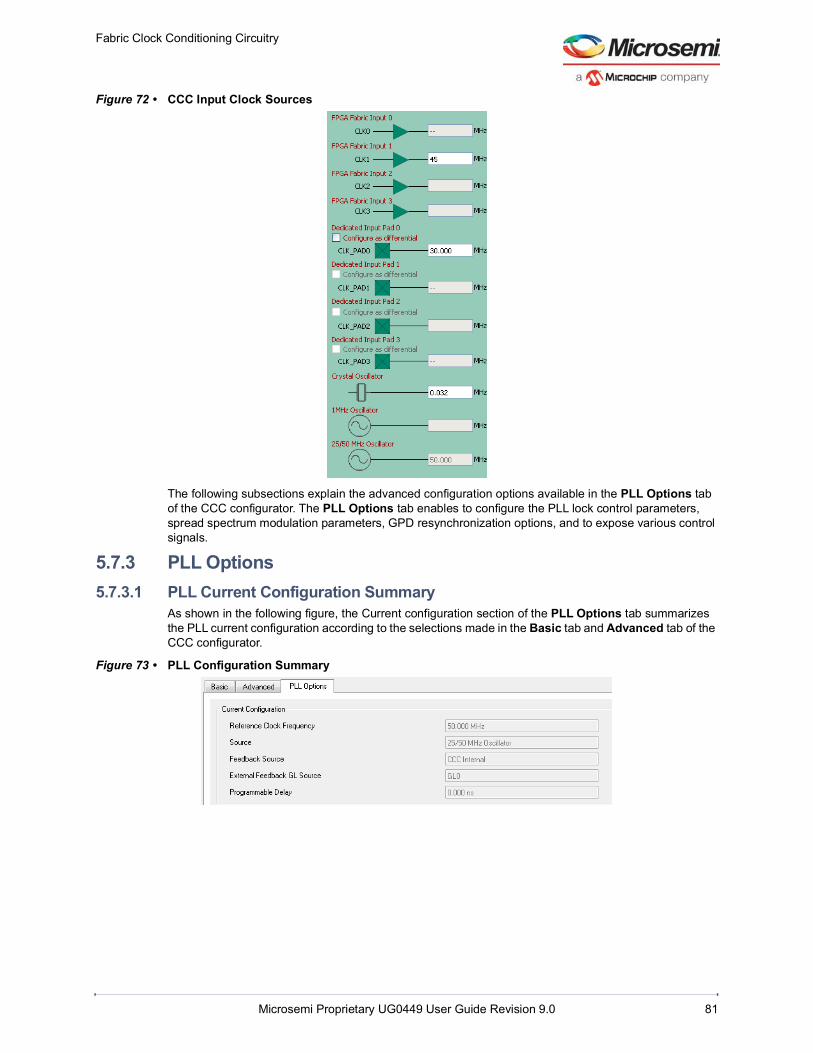
Fabric Clock Conditioning Circuitry
Microsemi Proprietary UG0449 User Guide Revision 9.0 81
Figure 72 • CCC Input Clock Sources
The following subsections explain the advanced configuration options available in the PLL Options tab of the CCC configurator. The PLL Options tab enables to configure the PLL lock control parameters, spread spectrum modulation parameters, GPD resynchronization options, and to expose various control signals.
5.7.3 PLL Options5.7.3.1 PLL Current Configuration Summary
As shown in the following figure, the Current configuration section of the PLL Options tab summarizes the PLL current configuration according to the selections made in the Basic tab and Advanced tab of the CCC configurator.
Figure 73 • PLL Configuration Summary

Fabric Clock Conditioning Circuitry
Microsemi Proprietary UG0449 User Guide Revision 9.0 82
5.7.3.2 PLL Lock ControlAs shown in the following figure, set the PLL lock control parameters, Lock window, and Lock delay, as appropriate for the design.
• Lock Window – Enables configuration of the maximum phase error allowed for the PLL to indicate it has been locked. The lock window is expressed as ppm of the RFCLK frequency.
Note: For SmartFusion2 and IGLOO2 devices, if the fabric PLL reference clock is sourced from an internal RC oscillator, the minimum PLL lock window setting should be 64000 ppm and 32000 ppm for 1 MHz RC oscillator and 50 MHz RC oscillator, respectively. If the RFDIV divisor value is 2 or less and a wrong PLL lock window setting is used, then the PLL lock may get toggled.The combination of high register utilization and toggling rate results high PLL jitter and subsequently the PLL may come out of lock. Use higher PLL lock window for stable PLL operation.
• Lock Delay – Enables configuration of the number of divided RFCLK clock cycles by which the lock is delayed after the PLL has reached the lock condition.
Figure 74 • PLL Lock Control Settings
5.7.3.3 Output Resynchronization ConfigurationEach fabric CCC contains four GPDs. The GPDs source and division settings are automatically configured based on the frequency requirement specified in the CCC configurator. Microsemi recommends to resynchronize the GPDs after the PLL lock is achieved.
The following figure shows the output resynchronization options available in the PLL Options tab. See the GPD Operating Modes, page 54 for more information on the GPD synchronization.
Figure 75 • GPD Synchronization Configuration
5.7.3.4 Spread Spectrum Clock Generation The PLL SSCG functionality can be enabled by selecting Enable PLL Spread Spectrum Modulation in the PLL Options tab. When the PLL SSCG functionality is enabled, the output frequency of the PLL is down-spread over time. The SSCG programmable options allow control of the modulation frequency and depth based on the design requirements. The CCC configurator forces the PLL feedback source to PLL internal when SSCG is enabled. See the SSCG, page 52 for more information on SSCG.
Figure 76 • PLL SSCG Configuration

Fabric Clock Conditioning Circuitry
Microsemi Proprietary UG0449 User Guide Revision 9.0 83
5.7.3.5 Miscellaneous OptionsThe following control signals can be exposed to the FPGA fabric:
• Dynamic configuration interface (APB3 slave)• PLL control signals (PLL_BYPASS_N, PLL_ARST_N, and PLL_POWERDOWN_N)• GPD asynchronous reset signals (GPDx_ARST_N with x= 0 to 3)These control signals are deasserted by default by the configurator when they are not exposed to the FPGA fabric. APB slave interfaces can be exposed for fabric CCC dynamic configuration. See the Functional Description, page 44 for more information on these control signals.
The following figure shows the miscellaneous options available for exposing fabric CCC control signals.
Figure 77 • Miscellaneous Options - Fabric CCC Control Signals
5.7.4 Simulation SupportMicrosemi Libero SoC design software provides pre-compiled simulation models for the CCC macro to show functional behavior of the fabric CCC. The simulation steps include generating the top-level component, which instantiates CCC macro, performing simulation for verification with the ModelSim tool, and performing static timing analysis with SmartTime in the Libero SoC software.
If the reference clock input of CCC is an oscillator, then clock constraint is automatically generated for the reference clock input of CCC and generated clock constraints are added in SmartTime for the CCC outputs. If the reference clock input of CCC is from FPGA Fabric Input or Dedicated Input Pad, the clock constraint is not generated for reference clock input of CCC but generated clock constraints are added in SmartTime for the CCC outputs. You need to add constraint on reference clock source output.
Note: The simulation models does not support PLL LOCK DELAY.
5.7.5 Clock Frequency SynthesisDeriving clocks of various frequencies from a single reference clock is known as frequency synthesis. This use model configures one of the on-chip oscillators as a clock source to the fabric CCC(s) and requires the instantiation of both the Chip Oscillators macro and CCC macro in the design. The Chip Oscillators macro must be configured to drive the CCC macro reference clock input. This use model uses the Basic tab of the CCC configurator for CCC configuration. See the How to Use On-Chip Oscillators, page 35 for on-chip oscillator configuration. It is also possible to use external clock sources through dedicated global I/Os instead of on-chip oscillators.
1. In the CCC configurator, select the output clocks and enter the desired clock frequencies. These frequencies are used by the CCC configurator to compute the configuration of the CCC dividers and PLL to meet the requirements. The Actual column displays the actual value that the configurator was able to achieve.• GL0 - 100 MHz• GL1 - 150 MHz• GL2 - 200 MHz

Fabric Clock Conditioning Circuitry
Microsemi Proprietary UG0449 User Guide Revision 9.0 84
Figure 78 • Output Clocks Settings
2. Select the fabric CCC reference clock input from the drop-down menu. For this use model, select the 50 MHz RC Oscillator as the clock source.
Figure 79 • Fabric CCC Reference Clock Selection
This configuration is sufficient for generating the desired clock frequencies.
3. Click OK to close the CCC configurator. 4. Connect the Chip Oscillators macro output to the CCC macro reference clock input. The following
figure shows the final SmartDesign component with CCC outputs promoted to top-level for simulation.
The generated clocks can then be connected to the fabric logic, external components through I/Os, or as a base clock to the SmartFusion2 and IGLOO2 hard IP blocks (MSS/HPMS, FDDR, and SERDESIF).
Figure 80 • FAB CCC and On-chip Oscillators Connectivity
Next, perform simulation in ModelSim to verify the generated output frequencies.

Fabric Clock Conditioning Circuitry
Microsemi Proprietary UG0449 User Guide Revision 9.0 85
5.7.6 Clock Delay AdjustmentFor PLLs, delays in the reference clock path enables clock delay and delay in the feedback clock path enables clock advancements with respect to the reference clock. A typical application for clock advancement is to advance the on-chip clock in order to cancel the global network delay and align the internal clock to an external clock on board.
Perform the fabric CCC basic configuration using the Basic tab of the CCC configurator as outlined in the Clock Frequency Synthesis, page 83. For clock delay adjustments, configure the fabric CCC programmable delay elements using the Advanced tab of the CCC configurator. Selecting a positive delay value enables the delay elements in the reference clock path to delay the output clock with respect to the PLL reference clock (Figure 81, page 85).
Selecting a negative delay value in the CCC configurator enables the delay element in the feedback clock path for the output clock advancement with respect to the PLL reference clock (Figure 82, page 85). Perform the timing analysis using SmartTime for the actual delay between the reference clock and output clocks.
Figure 81 • Clock Delay Simulation Waveform
Figure 82 • Clock Advancement Simulation Waveform
5.7.7 External Clock Source Through Dedicated Global I/OThis use model shows how to source the fabric CCC reference clock from an external clock source. Each fabric CCC is associated with four dedicated global I/Os for providing external reference clock.
The mapping of fabric CCCs is done by the Libero SoC place-and-route software based on the dedicated global I/O selected and the reference clock frequency. If the reference clock frequency is set to 32 KHz then the Libero SoC place-and-route software uses the CCC-NE1 and the external clock can come through the dedicated global I/Os associated with the CCC-NE1. The selection of the dedicated global I/Os is performed through I/O Attribute Editor of the Libero SoC design software.
Use the following steps to configure the fabric CCC with external reference clock:
1. Instantiate the CCC macro onto the SmartDesign canvas.2. In the CCC macro configurator,
• Select the output clocks and enter the desired clock frequencies.• Select one of the four dedicated global input pads as CCC reference clock source and set its
frequency, as shown in the following figure.
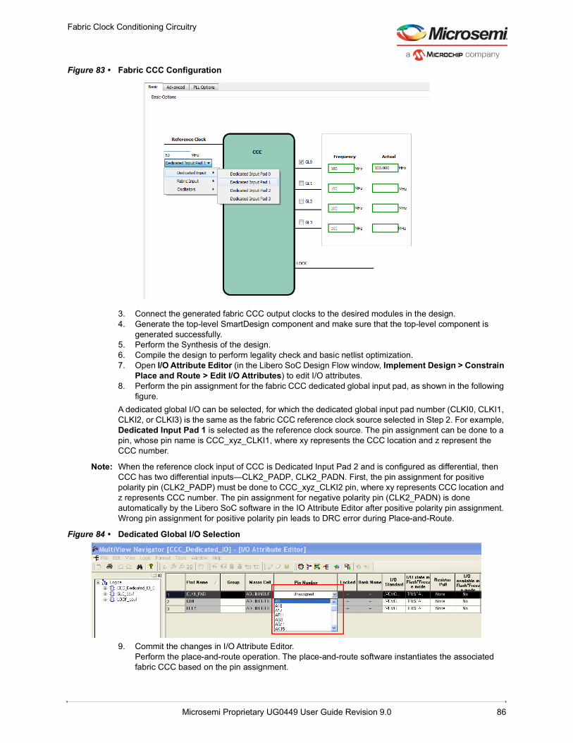
Fabric Clock Conditioning Circuitry
Microsemi Proprietary UG0449 User Guide Revision 9.0 86
Figure 83 • Fabric CCC Configuration
3. Connect the generated fabric CCC output clocks to the desired modules in the design.4. Generate the top-level SmartDesign component and make sure that the top-level component is
generated successfully.5. Perform the Synthesis of the design.6. Compile the design to perform legality check and basic netlist optimization.7. Open I/O Attribute Editor (in the Libero SoC Design Flow window, Implement Design > Constrain
Place and Route > Edit I/O Attributes) to edit I/O attributes.8. Perform the pin assignment for the fabric CCC dedicated global input pad, as shown in the following
figure. A dedicated global I/O can be selected, for which the dedicated global input pad number (CLKI0, CLKI1, CLKI2, or CLKI3) is the same as the fabric CCC reference clock source selected in Step 2. For example, Dedicated Input Pad 1 is selected as the reference clock source. The pin assignment can be done to a pin, whose pin name is CCC_xyz_CLKI1, where xy represents the CCC location and z represent the CCC number.
Note: When the reference clock input of CCC is Dedicated Input Pad 2 and is configured as differential, then CCC has two differential inputs—CLK2_PADP, CLK2_PADN. First, the pin assignment for positive polarity pin (CLK2_PADP) must be done to CCC_xyz_CLKI2 pin, where xy represents CCC location and z represents CCC number. The pin assignment for negative polarity pin (CLK2_PADN) is done automatically by the Libero SoC software in the IO Attribute Editor after positive polarity pin assignment. Wrong pin assignment for positive polarity pin leads to DRC error during Place-and-Route.
Figure 84 • Dedicated Global I/O Selection
9. Commit the changes in I/O Attribute Editor.Perform the place-and-route operation. The place-and-route software instantiates the associated fabric CCC based on the pin assignment.
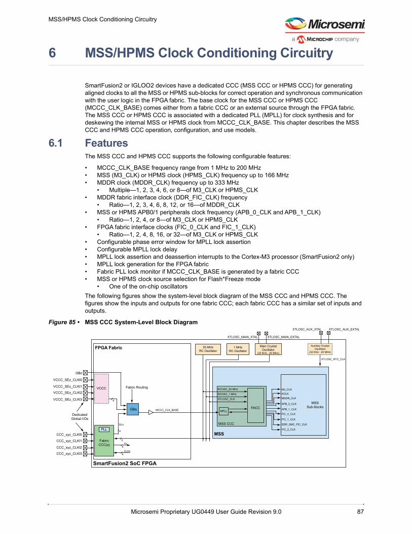
MSS/HPMS Clock Conditioning Circuitry
Microsemi Proprietary UG0449 User Guide Revision 9.0 87
6 MSS/HPMS Clock Conditioning Circuitry
SmartFusion2 or IGLOO2 devices have a dedicated CCC (MSS CCC or HPMS CCC) for generating aligned clocks to all the MSS or HPMS sub-blocks for correct operation and synchronous communication with the user logic in the FPGA fabric. The base clock for the MSS CCC or HPMS CCC (MCCC_CLK_BASE) comes either from a fabric CCC or an external source through the FPGA fabric. The MSS CCC or HPMS CCC is associated with a dedicated PLL (MPLL) for clock synthesis and for deskewing the internal MSS or HPMS clock from MCCC_CLK_BASE. This chapter describes the MSS CCC and HPMS CCC operation, configuration, and use models.
6.1 FeaturesThe MSS CCC and HPMS CCC supports the following configurable features:
• MCCC_CLK_BASE frequency range from 1 MHz to 200 MHz• MSS (M3_CLK) or HPMS clock (HPMS_CLK) frequency up to 166 MHz• MDDR clock (MDDR_CLK) frequency up to 333 MHz
• Multiple—1, 2, 3, 4, 6, or 8—of M3_CLK or HPMS_CLK• MDDR fabric interface clock (DDR_FIC_CLK) frequency
• Ratio—1, 2, 3, 4, 6, 8, 12, or 16—of MDDR_CLK• MSS or HPMS APB0/1 peripherals clock frequency (APB_0_CLK and APB_1_CLK)
• Ratio—1, 2, 4, or 8—of M3_CLK or HPMS_CLK• FPGA fabric interface clocks (FIC_0_CLK and FIC_1_CLK)
• Ratio—1, 2, 4, 8, 16, or 32—of M3_CLK or HPMS_CLK• Configurable phase error window for MPLL lock assertion• Configurable MPLL lock delay• MPLL lock assertion and deassertion interrupts to the Cortex-M3 processor (SmartFusion2 only)• MPLL lock generation for the FPGA fabric• Fabric PLL lock monitor if MCCC_CLK_BASE is generated by a fabric CCC• MSS or HPMS clock source selection for Flash*Freeze mode
• One of the on-chip oscillatorsThe following figures show the system-level block diagram of the MSS CCC and HPMS CCC. The figures show the inputs and outputs for one fabric CCC; each fabric CCC has a similar set of inputs and outputs.
Figure 85 • MSS CCC System-Level Block Diagram
CLKx
Yx
GLx
4
4
4
4
3
DedicatedGlobal I/Os
GBn
VCCC_SEz_CLKl3
CCC_xyz_CLKl0
CCC_xyz_CLKl1
CCC_xyz_CLKl2
CCC_xyz_CLKl3
VCCC_SEz_CLKl0
VCCC_SEz_CLKl1
VCCC_SEz_CLKl2Fabric Routing
MCCC_CLK_BASE
FIC_2_CLK
DDR_SMC_FIC_CLK
FIC_1_CLK
FIC_0_CLK
APB_0_CLK
APB_1_CLK
MDDR_CLKHCLKM3_CLK
MSSSub-blocks
XTLOSC_RTC_CLK
MSS
SmartFusion2 SoC FPGA
FPGA Fabric
MSS CCC
FACCMPLL
RCOSC_50 MHz
RCOSC_1 MHz
XTLOSC_CLK
FabricCCC(s)
PLL
VCCC
GBs
Auxilary CrystalOscillator
(32 KHz - 20 MHz)
50 MHzRC Oscillator
1 MHzRC Oscillator
Main CrystalOscillator
(32 KHz - 20 MHz)
XTLOSC_MAIN_XTAL
XTLOSC_AUX_XTAL
XTLOSC_MAIN_EXTAL
XTLOSC_AUX_EXTAL

MSS/HPMS Clock Conditioning Circuitry
Microsemi Proprietary UG0449 User Guide Revision 9.0 88
Figure 86 • HPMS CCC System-Level Block Diagram
6.2 Functional DescriptionThe MSS CCC or HPMS CCC consists of an MPLL and fabric alignment clock controller (FACC) that generates aligned clocks for MSS or HPMS operation and synchronous communication with the user logic. The following figures show aligned clocks (indicated in blue) generated by the MSS CCC or HPMS CCC and MSS or HPMS clocking scheme.
The following topics are covered in this section:
• MPLL• FACC• MSS CCC or HPMS CCC Operational Modes• PLLs Lock MonitoringSee the MSS CCC or HPMS CCC Configuration, page 97 for information on configuring the MSS CCC and HPMS CCC features.
CLKx
Yx
GLx
4
4
4
4
3
DedicatedGlobal I/Os
GBn
VCCC_SEz_CLKl3
CCC_xyz_CLKl0
CCC_xyz_CLKl1
CCC_xyz_CLKl2
CCC_xyz_CLKl3
VCCC_SEz_CLKl0
VCCC_SEz_CLKl1
VCCC_SEz_CLKl2Fabric Routing
MCCC_CLK_BASE
DDR_FIC_CLK
FIC_1_CLK
FIC_0_CLK
APB_0_CLK
APB_1_CLK
MDDR_CLKHCLKHPMS_CLK
HPMSSub-blocks
HPMS
IGLOO2
Fabric
HPMS CCC
FACCMPLL
RCOSC_50 MHz
RCOSC_1 MHz
XTLOSC_CLK
FabricCCC(s)
PLL
VCCC
GBs
50 MHzRC Oscillator
1 MHzRC Oscillator
Main CrystalOscillator
(32 KHz - 20 MHz)
XTLOSC_MAIN_XTAL XTLOSC_MAIN_EXTAL
FIC_2_CLK

MSS/HPMS Clock Conditioning Circuitry
Microsemi Proprietary UG0449 User Guide Revision 9.0 89
Figure 87 • SmartFusion2 MSS Clocking Scheme
Cortex-M3Processor
Cache Controller
AHB Bus Matrix
MSS DDRBridge
HPDMA
MSS DDR
Peripherals
Peripherals
FIC_1FIC_0MDDR_FIC/SMC_FIC
M3_CLK
MDDR_CLK
DDR_SMC_FIC_CLK
APB_0_CLK
APB_1_CLK
MC
CC
_CLK
_BAS
E
MDDR_FIC/SMC_FICFPGA Fabric Subsystem
FIC_0 FPGA fabric Subsystem
FIC_1 FPGA fabric Subsystem
DDR_SMC_FIC_CLK
Fabric CCC
FPGA Fabric
Smallest Frequency
APB_1 APB_0
MSS
SmartFusion2
FACC
MPLL
FIC_0_CLK
FIC_0_CLK
FIC_1_CLK
FIC_1_CLK
MSS CCC

MSS/HPMS Clock Conditioning Circuitry
Microsemi Proprietary UG0449 User Guide Revision 9.0 90
Figure 88 • IGLOO2 FPGA HPMS Clocking Scheme
6.2.1 MPLLThe MCCC_CLK_BASE from the FPGA fabric is used as a reference clock to the MPLL, and is multiplied to generate a clock frequency of up to 333 MHz. The MCCC_CLK_BASE can be generated from a fabric CCC/PLL, one of the on-chip oscillators, or an external source through a dedicated global I/O.
The supplies required to power the MPLL are the VDD for the digital section and analog supply (MDDR_PLL_VDDA) for the analog section. The MDDR_PLL_VDDA can be either 2.5 V or 3.3 V, based on the power supply availability on board. The analog power supply voltage (2.5 V or 3.3 V) does not impact the MPLL frequency range. The PLL analog supply voltage is internally regulated, which provides independence from the external supply. See SmartFusion2 and IGLOO2 Datasheet for the MPLL operational range and characteristics.
The MPLL generates a lock signal (MCCC_MPLL_LOCK) to indicate that the MPLL is locked on to the MCCC_CLK_BASE signal. The precision of the MCCC_MPLL_LOCK discrimination can be adjusted using the lock window controls. The lock window represents the phase error window for lock assertion. The lock window can be adjusted between 500 ppm and 32,000 ppm in powers of 2. The integration of the lock period can be adjusted using a built-in lock counter. The lock counter or lock delay indicates the number of divided reference clock cycles to wait after the MPLL is locked before asserting the MCCC_MPLL_LOCK signal. The lock delay is useful for avoiding false toggling of the MPLL lock signal. The lock counter can be configured between 32 and 32,768 cycles in multiples of 2.
There are two interrupts connected to the NVIC of the Cortex-M3 processor to indicate the MPLL lock assertion and deassertion. The MCCC_MPLL_LOCK signal can be monitored by the user logic in the FPGA fabric.
AHB Bus Matrix
HPMS DDRBridge
HPDMA
HPMS DDR
SPI
COMM_BLK
FIC_1FIC_0MDDR_FIC
HPMS_CLK
MDDR_CLK
DDR_FIC_CLK
APB_0_CLK
APB_1_CLK
MC
CC
_CLK
_BAS
E
MDDR_FICFPGA Fabric Subsystem
FIC_0 FPGA fabric Subsystem
FIC_1 FPGA fabric Subsystem
DDR_FIC_CLK
Fabric CCC
Fabric
Smallest Frequency
APB_1 APB_0
HPMSIGLOO2
FACC
MPLL
FIC_0_CLK
FIC_0_CLK
FIC_1_CLK
FIC_1_CLK
HPMS CCC

MSS/HPMS Clock Conditioning Circuitry
Microsemi Proprietary UG0449 User Guide Revision 9.0 91
6.2.2 FACCWithin the MSS or HPMS CCC, the FACC is responsible for interfacing with the MPLL, generating the various aligned clocks required by the MSS or HPMS sub-blocks, and controlling the alignment of the FPGA fabric interface clocks. The following figure shows the functional block diagram of the FACC.
Figure 89 • FACC Functional Block Diagram of SmartFusion2 and IGLOO2
The following table lists clocks generated by the FACC.
Table 54 • Clocks Generated by FACC
Clock Name DescriptionMDDR_CLK Clocks the MDDR subsystem and the MSS or HPMS DDR bridge. It can be operated
up to 333 MHz depending on DDR memory type that is present in the system.
M3_CLK or HPMS_CLK and HCLK
M3_CLK is used within the MSS to clock the Cortex-M3 processor, HPDMA, and the AHB bus matrix. HPMS_CLK is used within the HPMS to clock the AHB bus matrix and HPDMA. HCLK always at the same frequency as the M3_CLK or HPMS_CLK but is a gated version of it. M3_CLK/HPMS_CLK maximum frequency is dependent on device speed grade. For -1 speed grade, the maximum frequency is 166 MHz and for standard speed grade, it is 142 MHz.
APB_0_CLK/PCLK0 Clocks all the peripherals connected on the APB_0 bus.
APB_1_CLK/PCLK1 Clocks all the peripherals connected on the APB_1 bus.
FIC_0_CLK and FIC_1_CLK Clock the MSS or HPMS FIC_0 and FIC_1 interfaces respectively. These clocks define the frequency at which the connected FPGA fabric subsystem is intended to operate.
FIC_2_CLK Clocks the APB configuration interface (FIC_2), FIC_2 clock is M3_CLK or HPMS_CLK divided by 4.
RC Osc Fabric
ClockGate
ClockGate
Stage ADivider
Stage BDivider
Standby Multiplexer
Output NGMUXs
XTLOSC_CLK
MC
CC
_CLK
_BAS
E
RC
OSC
_25_
50M
HZ
RC
OSC
_1M
HZ
MPLL_REF_CLK
DDR_SMC_FIC_CLK/DDR_FIC_CLK
APB _0_CLK
M3_CLK/HPMS_CLK
MDDR_CLKCLK_SRC
CLK_A
CLK_STANDBY
HCLK
APB_1_CLK
FIC_2_CLK
MPLL_OUT_CLK
MPL
LXT
ALM
SS/HPM
SM
DD
R_SU
BSYS
÷ 1
÷ 2
÷ 3
÷ 4
÷ 4
÷ 1÷ 2
÷ 8
÷ 16
÷ 32
00
00000101x10010111x
00000101x
10010111x
00000101x
10010111x
00000101x
10010111x
01
1x
1
0
1
0
1
0
10
1
0
1[0]
[1]
0

MSS/HPMS Clock Conditioning Circuitry
Microsemi Proprietary UG0449 User Guide Revision 9.0 92
6.2.2.1 FACC DividersThe FACC consists of two stages of clock dividers: Stage A and Stage B. These stages divide the high-speed clock coming from the MPLL to generate the aligned clocks according to the configured division ratios. These aligned clocks can be at different frequencies to each other, but the rising edges of slower clocks occur coincidentally with the rising edges of faster clocks.
As shown in Figure 89, page 91, the Stage A divider divides the MDDR_CLK by 1, 2, or 3, to feed CLK_A into the Stage B divider. The Stage B divider has a number of outputs, which select the division by 1, 2, 4, 8, 16, or 32. Each of the MSS and HPMS clocks can be configured to select one of these divider taps.
Following are the MSS and HPMS clocks configuration constraints. These constraints are automatically checked by the MSS_CCC and IGLOO2 System Builder in the Libero SoC software.
1. Maximum frequency of MDDR_CLK is 333 MHz.2. Maximum frequency of M3_CLK and HPMS_CLK is 166 MHz for -1 speed grade and 142 MHz for
standard speed grade.3. Maximum frequency of DDR_SMC_FIC_CLK and DDR_FIC_CLK is 200 MHz4. M3_CLK must be greater than 30 MHz when the MSS USB interface is enabled.5. The MCCC_CLK_BASE must be the lowest of any aligned clocks interfacing between the MSS or
HPMS and the FPGA fabric.6. The possible MDDR_CLK:M3_CLK or HPMS_CLK ratios are 1:1, 2:1, 3:1, 4:1, 6:1, or 8:1.7. The APB_0_CLK and APB_1_CLK may have different frequencies from each other but both must be
equal to, or slower than M3_CLK or HPMS_CLK. The possible M3_CLK or HPMS_CLK:APB_0_CLK/APB_1_CLK ratios are 1:1, 2:1, 4:1, or 8:1.
8. Only in the SmartFusion2 device, in soft memory controller (SMC) mode (that is, when the SMC_FIC block is operational), the MDDR_CLK and DDR_SMC_FIC_CLK must run at the same speed as to the M3_CLK.
9. When MDDR_FIC is operational, DDR_FIC_CLK must run at the same speed or slower than the MDDR_CLK. Possible configurations for DDR_FIC_CLK:• If MDDR_CLK is 3, 6 multiples of M3_CLK or HPMS_CLK then DDR_FIC_CLK must be
MDDR_CLK/n where n={3,6,12}• If MDDR_CLK is 1, 2, 4, 8 multiples of M3_CLK or HPMS_CLK then DDR_FIC_CLK must be
MDDR_CLK/n where n={1,2,4,8,16}10. Each FPGA fabric FIC subsystem must be driven by a clock with a frequency matching the
respective FIC interface clock frequency defined in the MSS CCC or HPMS CCC.11. Only in the SmartFusion2 device, if the CAN peripheral within the MSS is operational, then
APB_1_CLK must be a multiple of 8 MHz, which implies that M3_CLK must be a multiple of 8.The following figure shows several example aligned clock configurations for MDDR_CLK and M3_CLK or HPMS_CLK. In all the configurations, the MSS or HPMS peripherals and fabric subsystems can run at different clock ratios independently as per the constraints listed above.
DDR_SMC_FIC_CLK or DDR_FIC_CLK
Clocks the MDDR_FIC or SMC_FIC, and defines the frequency at which the connected FPGA fabric subsystem is intended to operate.
Table 54 • Clocks Generated by FACC (continued)
Clock Name Description

MSS/HPMS Clock Conditioning Circuitry
Microsemi Proprietary UG0449 User Guide Revision 9.0 93
Figure 90 • Aligned Clock Configuration Examples
6.2.2.2 No-Glitch MultiplexersThe FACC includes no-glitch multiplexers (NGMUXs) to feed the MSS or HPMS clocks with a standby clock (CLK_STANDBY) during the MPLL initialization, Flash*Freeze mode, or in the second stage of in-application programming (IAP), when the FPGA fabric is not valid (MCCC_CLK_BASE is not usable) as shown in the following figure.
The standby multiplexer selects the output of one of the three on-chip oscillators as the standby clock. During MPLL initialization, the standby multiplexer is automatically configured to select the 50 MHz RC oscillator as the standby clock. The standby clock during Flash*Freeze mode can be configured to come from the 1 MHz RC oscillator, or 50 MHz RC oscillator. For IAP, the standby multiplexer must be configured to select the 50 MHz RC oscillator as the clock source, before requesting IAP from the System Controller.
There are four other NGMUXs available at outputs to switch the MSS or HPMS clocks cleanly between the CLK_STANDBY and the MPLL derived clock, as shown in the following figure. All four of these NGMUXs switch at the same time.
333 MHz
166 MHz
111 MHz
83 MHz
41 MHz
300 MHz
150 MHz
100 MHz
75 MHz
266 MHz
133 MHz
66 MHz
33 MHz
50 MHz
Configuration3 (MDDR max = 266 MHz)(mddr_clk@266MHz)(MSS/HPMS: m3_clk/hpms_clk@133-/66-/33 MHz)
Configuration2 (MDDR max = 300 MHz)(mddr_clk@300MHz)(MSS/HPMS: m3_clk/hpms_clk@150-/100-/ 75-/50 MHz)
Configuration1 (MDDR max = 333 MHz)(mddr_clk@333MHz)(MSS/HPMS: m3_clk/hpms_clk@166-/111-/83-/41 MHz)
In all configurations, MSS/HPMS peripherals and fabric mayrun independently at differentratios.

MSS/HPMS Clock Conditioning Circuitry
Microsemi Proprietary UG0449 User Guide Revision 9.0 94
Figure 91 • FACC Functional Block Diagram—No-Glitch Multiplexers
When CLK_STANDBY is used for MSS or HPMS clocking:
• M3_CLK or HPMS_CLK and APB_0_CLK/APB_1_CLK are the same as CLK_STANDBY• MDDR_CLK is gated offFor Flash*Freeze mode, the switching of the clock source to use the selected standby clock is done automatically by the System Controller upon receiving a Flash*Freeze entry request message. When a Flash*Freeze exit condition is detected, the System Controller switches the clock source of the MSS or HPMS back to the MPLL output without any glitches. The System Controller also switches the clock source to the standby clock during the second stage of IAP.
6.2.2.2.1 MSS Clock Switching from User Clock to Standby ClockIn SmartFusion2 devices, when the clock source for the M3_CLK switches from user clock (CLK_SRC) to standby clock (CLK_STANDBY), there is a possibility for both M3_CLK and FIC_2_CLK to halt if a wrong Stage B divisor is used within the FACC, see Figure 91, page 94. The Stage B divider must be set with correct divisor value before initiating MSS clock switching from user clock to standby clock. The following table lists required Stage B divider setting for proper MSS clock switching from user clock to standby clock.
Table 55 • Stage B Divider setting for MSS Clock Switching from User Clock to Standby Clock
SmartFusion2 Device Stage B Clock Divisor to use5 Divide by 32
10 Divide by 32
25 Divide by 32
50 Divide by 32
60 Any divider except divide by 32
RC Osc Fabric
ClockGate
ClockGate
Stage ADivider
Stage BDivider
Standby Multiplexer
Output NGMUXs
XTLOSC_CLK
MC
CC
_CLK
_BAS
E
RC
OSC
_25_
50M
HZ
RC
OSC
_1M
HZ
MPLL_REF_CLK
DDR_SMC_FIC_CLK/DDR_FIC_CLK
APB _0_CLK
M3_CLK/HPMS_CLK
MDDR_CLKCLK_SRC
CLK_A
CLK_STANDBY
HCLK
APB_1_CLK
FIC_2_CLK
MPLL_OUT_CLK
MPL
LXT
ALM
SS/HPM
SM
DD
R_SU
BSYS
÷ 1
÷ 2
÷ 3
÷ 4
÷ 4
÷ 1÷ 2
÷ 8
÷ 16
÷ 32
00
00000101x10010111x
00000101x
10010111x
00000101x
10010111x
00000101x
10010111x
01
1x
1
0
1
0
1
0
10
1
0
1[0]
[1]
0
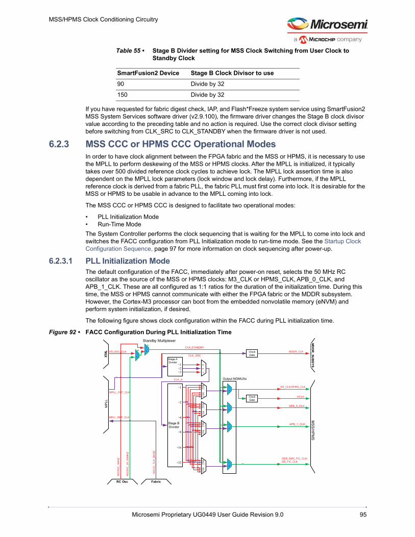
MSS/HPMS Clock Conditioning Circuitry
Microsemi Proprietary UG0449 User Guide Revision 9.0 95
If you have requested for fabric digest check, IAP, and Flash*Freeze system service using SmartFusion2 MSS System Services software driver (v2.9.100), the firmware driver changes the Stage B clock divisor value according to the preceding table and no action is required. Use the correct clock divisor setting before switching from CLK_SRC to CLK_STANDBY when the firmware driver is not used.
6.2.3 MSS CCC or HPMS CCC Operational ModesIn order to have clock alignment between the FPGA fabric and the MSS or HPMS, it is necessary to use the MPLL to perform deskewing of the MSS or HPMS clocks. After the MPLL is initialized, it typically takes over 500 divided reference clock cycles to achieve lock. The MPLL lock assertion time is also dependent on the MPLL lock parameters (lock window and lock delay). Furthermore, if the MPLL reference clock is derived from a fabric PLL, the fabric PLL must first come into lock. It is desirable for the MSS or HPMS to be usable in advance to the MPLL coming into lock.
The MSS CCC or HPMS CCC is designed to facilitate two operational modes:
• PLL Initialization Mode• Run-Time ModeThe System Controller performs the clock sequencing that is waiting for the MPLL to come into lock and switches the FACC configuration from PLL Initialization mode to run-time mode. See the Startup Clock Configuration Sequence, page 97 for more information on clock sequencing after power-up.
6.2.3.1 PLL Initialization ModeThe default configuration of the FACC, immediately after power-on reset, selects the 50 MHz RC oscillator as the source of the MSS or HPMS clocks: M3_CLK or HPMS_CLK, APB_0_CLK, and APB_1_CLK. These are all configured as 1:1 ratios for the duration of the initialization time. During this time, the MSS or HPMS cannot communicate with either the FPGA fabric or the MDDR subsystem. However, the Cortex-M3 processor can boot from the embedded nonvolatile memory (eNVM) and perform system initialization, if desired.
The following figure shows clock configuration within the FACC during PLL initialization time.
Figure 92 • FACC Configuration During PLL Initialization Time
90 Divide by 32
150 Divide by 32
Table 55 • Stage B Divider setting for MSS Clock Switching from User Clock to Standby Clock
SmartFusion2 Device Stage B Clock Divisor to use
RC Osc Fabric
MD
DR_SU
BSYS
Stage BDivider
Clock Gate
M3_CLK/HPMS_CLK
HCLK
CLK_STANDBY
CLK_SRC
MPLL_REF_CLK
Clock Gate
DDR_SMC_FIC_CLK/DR_FIC_CLK
MDDR_CLK
÷1
÷2
÷4
÷8
÷16
÷32
XTAL
MPLL_OUT_CLK
MPL
L
Stage ADivider
÷1
÷2
÷3
Standby Multiplexer
CLK_A
1
0
1
0
1
0
1
0
1
0
1
0
00000101x
10010111x
00000101x
10010111x
00000101x
10010111x
00000101x
10010111x
00
01
1x
[0]
[1]
XTLOSC_CLK
RC
OSC
_1M
HZ
RC
OSC
_25_
50M
HZ
MC
CC
_CLK
_BAS
E
APB_0_CLK
APB_1_CLK
Output NGMUXs
MSS/H
PMS
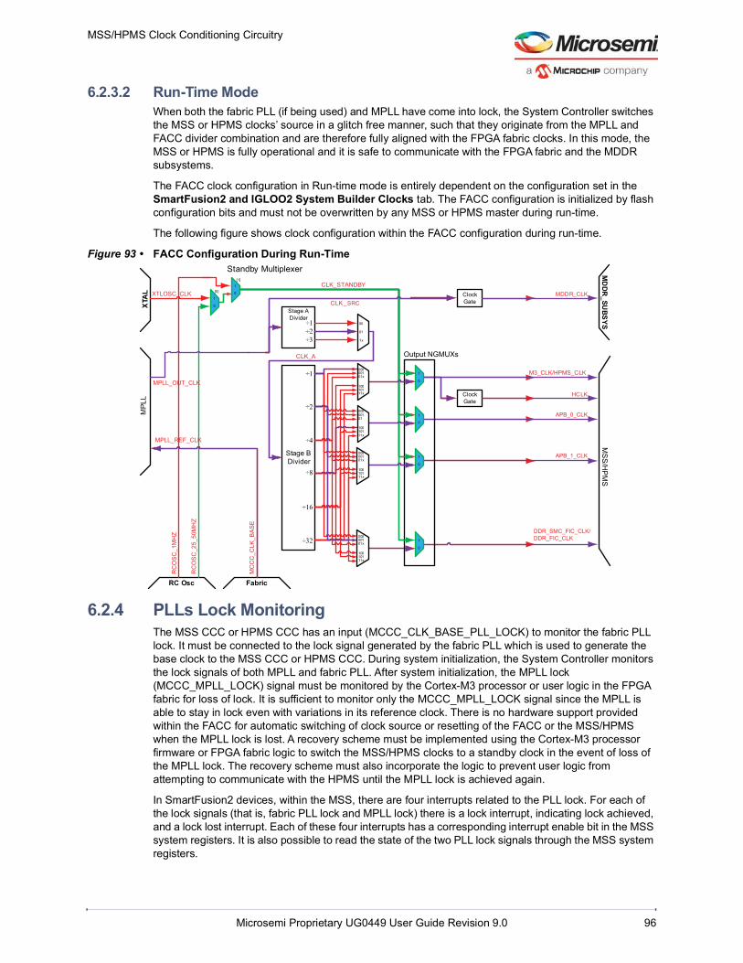
MSS/HPMS Clock Conditioning Circuitry
Microsemi Proprietary UG0449 User Guide Revision 9.0 96
6.2.3.2 Run-Time ModeWhen both the fabric PLL (if being used) and MPLL have come into lock, the System Controller switches the MSS or HPMS clocks’ source in a glitch free manner, such that they originate from the MPLL and FACC divider combination and are therefore fully aligned with the FPGA fabric clocks. In this mode, the MSS or HPMS is fully operational and it is safe to communicate with the FPGA fabric and the MDDR subsystems.
The FACC clock configuration in Run-time mode is entirely dependent on the configuration set in the SmartFusion2 and IGLOO2 System Builder Clocks tab. The FACC configuration is initialized by flash configuration bits and must not be overwritten by any MSS or HPMS master during run-time.
The following figure shows clock configuration within the FACC configuration during run-time.
Figure 93 • FACC Configuration During Run-Time
6.2.4 PLLs Lock MonitoringThe MSS CCC or HPMS CCC has an input (MCCC_CLK_BASE_PLL_LOCK) to monitor the fabric PLL lock. It must be connected to the lock signal generated by the fabric PLL which is used to generate the base clock to the MSS CCC or HPMS CCC. During system initialization, the System Controller monitors the lock signals of both MPLL and fabric PLL. After system initialization, the MPLL lock (MCCC_MPLL_LOCK) signal must be monitored by the Cortex-M3 processor or user logic in the FPGA fabric for loss of lock. It is sufficient to monitor only the MCCC_MPLL_LOCK signal since the MPLL is able to stay in lock even with variations in its reference clock. There is no hardware support provided within the FACC for automatic switching of clock source or resetting of the FACC or the MSS/HPMS when the MPLL lock is lost. A recovery scheme must be implemented using the Cortex-M3 processor firmware or FPGA fabric logic to switch the MSS/HPMS clocks to a standby clock in the event of loss of the MPLL lock. The recovery scheme must also incorporate the logic to prevent user logic from attempting to communicate with the HPMS until the MPLL lock is achieved again.
In SmartFusion2 devices, within the MSS, there are four interrupts related to the PLL lock. For each of the lock signals (that is, fabric PLL lock and MPLL lock) there is a lock interrupt, indicating lock achieved, and a lock lost interrupt. Each of these four interrupts has a corresponding interrupt enable bit in the MSS system registers. It is also possible to read the state of the two PLL lock signals through the MSS system registers.
MSS/H
PMS
RC Osc Fabric
MD
DR_SU
BSYS
MDDR_CLK
Stage BDivider
Clock Gate
CLK_STANDBY
CLK _SRC
Clock Gate
HCLK
DDR_SMC_FIC_CLK/DDR_FIC_CLK
÷1
÷2
÷4
÷8
÷16
÷32
XTAL
MPLL_OUT_CLK
MPL
L
Stage ADivider
÷1
÷2
÷3
Standby Multiplexer
CLK_A
1
0
1
0
1
0
1
0
1
0
1
0
00000101x
10010111x
00000101
10010111x
00000101x
10010111x
00000101x
10010111x
00
01
1x
[0]
[1]
XTLOSC_CLK
RC
OSC
_1M
HZ
RC
OSC
_25_
50M
HZ
MC
CC
_CLK
_BAS
E
APB_0_CLK
APB_1_CLK
Output NGMUXs
MPLL_REF_CLK
M3_CLK/HPMS_CLK

MSS/HPMS Clock Conditioning Circuitry
Microsemi Proprietary UG0449 User Guide Revision 9.0 97
In the event of loss of MPLL lock, even though its output is not exactly in phase lock with the reference, the MPLL still generates a clock. Due to the fact that the clock continues to run (though possibly not fully frequency—or phase—aligned with the reference clock), loss of lock is not considered a catastrophic event for the MSS or HPMS CCC. In SmartFusion2 devices, since the Cortex-M3 processor is running, firmware can use the loss of lock interrupt to take precautionary action, in a controlled way such as the following:
• Executing a recovery routine from embedded SRAM (eSRAM) by switching the clock source to the 50 MHz RC oscillator
• Disabling communications with the FPGA fabric (as the fabric and MSS clocks may be misaligned, if the PLLs are not in lock).
User logic in the FPGA fabric can use the MCCC_MPLL_LOCK signal to prevent user logic from attempting to communicate with the MSS during this time.
6.3 Startup Clock Configuration SequenceThis section summarizes the SmartFusion2 MSS or IGLOO2 HPMS clock configuration sequence from power-on reset.
1. After power-on reset, the MSS or HPMS is clocked by the 50 MHz RC oscillator through the CLK_STANDBY path. • MDDR is in reset during clock start-up. • User logic in the FPGA fabric can use the MPLL lock signal to prevent logic from attempting to
communicate with the MSS or HPMS during this time. • The MSS or HPMS can continue to run in a limited mode (no FIC transactions) for executing
initialization code.2. Flash configuration bits configure fabric CCC/PLL, MPLL, and FACC dividers for desired clock
configuration. • MCCC_CLK_BASE is provided to the MPLL reference input.• Waits for the fabric CCC/PLL lock, if it is being used. • Waits until MPLL comes into lock.
3. Upon lock, the System Controller switches M3_CLK or HPMS_CLK, HCLK, APB_0_CLK, APB_1_CLK, and DDR_FIC_CLK NGMUXs to source from the FACC clock dividers.
4. Releases reset of the MDDR and fabric interfaces.
6.4 MSS CCC or HPMS CCC ConfigurationThe MSS or HPMS clocks are statically configured through the MSS clock configurator (MSS_CCC) or IGLOO2 System Builder (Clocks tab) in the Libero SoC software. The MSS_CCC configurator or IGLOO2 System Builder derives the necessary MPLL internal divider ratios and selects the FACC dividers ratios based on the MCCC_CLK_BASE and the desired output frequencies. After power-on reset, the MSS CCC or HPMS CCC is initialized with these configuration values.
The MSS CCC or HPMS CCC configuration is controlled by the SYSREG control registers. However, Microsemi recommends that the MSS CCC or HPMS CCC must be configured at the programming stage through flash bits set by the MSS_CCC configurator or IGLOO2 System Builder and not to be modified dynamically during run-time. It is possible to read the state of the MPLL lock signal through the MSS system registers. See the SYSREG Control Registers, page 107 for HPMS CCC configuration.

MSS/HPMS Clock Conditioning Circuitry
Microsemi Proprietary UG0449 User Guide Revision 9.0 98
6.5 How to Use MSS CCCThis section describes how to use the clocks in the SmartFusion2 devices. To configure the SmartFusion2 device features and then build a complete system, use the System Builder graphical design wizard in the Libero SoC software.
The following figure shows the initial System Builder window where you can select the device features that you require. For details on how to launch the System Builder wizard and a detailed information on how to use it, see SmartFusion2 System Builder User Guide.
Figure 94 • System Builder Window
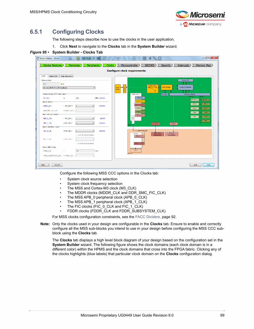
MSS/HPMS Clock Conditioning Circuitry
Microsemi Proprietary UG0449 User Guide Revision 9.0 99
6.5.1 Configuring ClocksThe following steps describe how to use the clocks in the user application.
1. Click Next to navigate to the Clocks tab in the System Builder wizard.Figure 95 • System Builder - Clocks Tab
Configure the following MSS CCC options in the Clocks tab:• System clock source selection• System clock frequency selection• The MSS and Cortex-M3 clock (M3_CLK)• The MDDR clocks (MDDR_CLK and DDR_SMC_FIC_CLK)• The MSS APB_0 peripheral clock (APB_0_CLK)• The MSS APB_1 peripheral clock (APB_1_CLK)• The FIC clocks (FIC_0_CLK and FIC_1_CLK)• FDDR clocks (FDDR_CLK and FDDR_SUBSYSTEM_CLK)
For MSS clocks configuration constraints, see the FACC Dividers, page 92.
Note: Only the clocks used in your design are configurable in the Clocks tab. Ensure to enable and correctly configure all the MSS sub-blocks you intend to use in your design before configuring the MSS CCC sub-block using the Clocks tab.
The Clocks tab displays a high level block diagram of your design based on the configuration set in the System Builder wizard. The following figure shows the clock domains (each clock domain is in a different color) within the HPMS and the clock domains that cross into the FPGA fabric. Clicking any of the clocks highlights (blue labels) that particular clock domain on the Clocks configuration dialog.

MSS/HPMS Clock Conditioning Circuitry
Microsemi Proprietary UG0449 User Guide Revision 9.0 100
Figure 96 • Clocks Tab Showing the Clock Paths Preview
2. Select the desired System Clock source. Based on the clock source selection, system builder instantiate and configure the CCC macro and chip oscillators macro.
Figure 97 • Clock Source Selection
3. Configure the clock frequency of the MSS and Cortex-M3 processor (M3_CLK). This specifies the frequency of the Cortex-M3 processor, AHB bus matrix, HPDMA, eNVM, and eSRAM.
4. MDDR clocks consist of two clock domains: MDDR_CLK and DDR_SMC_FIC_CLK• Configure MDDR_CLK as a multiple—1, 2, 3, 4, 6, or 8—of the M3_CLK.• Configure DDR/SMC_FIC_CLK as a ratio—1, 2, 3, 4, 6, 8, 12, or 16—of the MDDR_CLK.

MSS/HPMS Clock Conditioning Circuitry
Microsemi Proprietary UG0449 User Guide Revision 9.0 101
5. Configure the MSS APB_0 Clock for peripherals connected to APB_0 bus.6. Configure the MSS APB_1 Clock for peripherals connected to APB_1 bus.7. Configure the Fabric Interface Clocks (FIC_0_CLK and FIC_1_CLK) as a ratio—1, 2, 4, 8, 16, or
32—of M3_CLK such that the generated frequencies meet the timing requirements of the logic implemented in the FPGA fabric for each FIC subsystem.
8. Configure the FIC subsystem clocks as a ratio—1, 2, 4, 8, 16, or 32—of M3_CLK. Verify the timing for each FIC subsystem if it meets the selected clock frequency by performing timing analysis of the design using SmartTime.
6.5.2 How to Clock MSS and FIC Subsystems for Synchronous communicationThe following rules of the SmartFusion2 architecture must be followed for synchronous communication between the MSS and FPGA fabric FIC subsystems.
• Drive each FPGA fabric FIC subsystem by a clock with a frequency that matches the frequency defined for that particular subsystem in the Clocks configuration tab in System Builder wizard.
• The FPGA fabric FIC subsystem clock with the smallest frequency must drive the MSS CLK_BASE.• Align all the FPGA fabric FIC subsystem clocks precisely; the clocks could be of different
frequencies, but align the rising-edges of the slower clocks to the rising-edges of the fastest clocks.The following figure shows the clocking scheme that must be followed for synchronous communication between MSS and FPGA fabric.
Figure 98 • Clocking Scheme for Synchronous Communication Between MSS and FPGA Fabric
Use the following steps to configure the clock networks for all the FIC subsystems.
1. Configure the SmartFusion2 MSS peripheral components and FIC interfaces (FIC_0, FIC_1, and/or DDR_FIC) according to the design requirements using the System Builder.See SmartFusion2 System Builder User Guide for more information on how to create FIC subsystem in FPGA fabric.
2. Configure the MSS Clock, MDDR Clocks, MSS APB Clocks, and Fabric Interface Clocks in the Clocks tab.
CLK
_BAS
E
The MSS and FPGA fabricFIC clocks must have
matching frequencies for each FIC subsystem
The slowest of the FPGAfabric FIC clocks must drivethe MSS CLK_BASE port
The FPGA fabric FIC clocksmust be aligned
Fabric
MSS
CCC/PLL
MSS_CCC
DDR-CTRL DDR Bridge
Cortex-M3
Cache Controller
HPDMA SWITCHM3_CLK
MDDR_CLK
DDR_SMC_FIC_CLK
APB_0_CLK
APB_0 APB_1
APB_1_CLK
FIC_1_CLK
FIC_0_CLK
DDR_SMC_FIC_CLK
FIC_1_CLK
FIC_0_CLK
SMC_FIC FPGA Fabric Subsystem
FIC_1 FPGAFabric Subsystem
FIC_0 FPGAFabric Subsystem
SMC_FIC FIC_0 FIC_1
MMUART_0 MMUART_1
SPI_0 SPI_1
I2C_0 I2C_1
DMA CAN
WD GPIO
RTC
Lowest frequency

MSS/HPMS Clock Conditioning Circuitry
Microsemi Proprietary UG0449 User Guide Revision 9.0 102
Figure 99 • MSS CCC Clock Configuration
3. Proceed with the rest of the configurations in the System Builder wizard and create the subsystem.4. The System Builder generated subsystem exposes the FIC clocks (FIC_0_CLK and FIC_1_CLK)
and corresponding lock signals (FIC_0_LOCK and FIC_1_LOCK) to the FPGA fabric. Connect the FIC clocks to the fabric master and/or slave clock inputs for synchronous operation with the MSS. The FIC_0_LOCK and FIC_1_LOCK signals can be used to monitor the state of the FIC clocks.
6.6 How to Use HPMS ClocksThis section describes how to use the clocks in the IGLOO2 devices. To configure the IGLOO2 device features and then build a complete system, use the System Builder graphical design wizard in the Libero SoC software.
Figure 100 • Fabric Clocks Configuration

MSS/HPMS Clock Conditioning Circuitry
Microsemi Proprietary UG0449 User Guide Revision 9.0 103
The following figure shows the initial System Builder window where you can select the device features that you require. For details on how to launch the System Builder wizard and a detailed information on how to use it, refer the IGLOO2 System Builder User Guide.
Figure 101 • System Builder Window
6.6.1 Configuring ClocksThe following steps describe how to use the clocks in the user application.
1. Click Next to navigate to the Clocks tab in the System Builder wizard.Figure 102 • System Builder - Clocks Tab
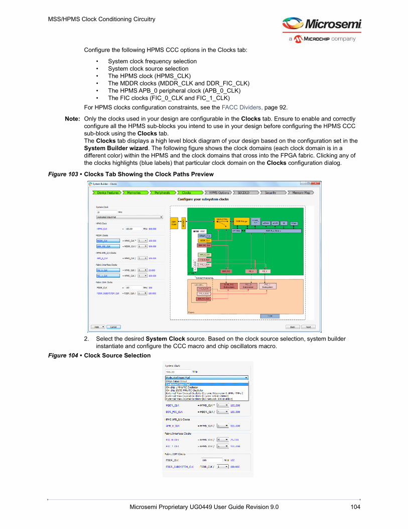
MSS/HPMS Clock Conditioning Circuitry
Microsemi Proprietary UG0449 User Guide Revision 9.0 104
Configure the following HPMS CCC options in the Clocks tab:
• System clock frequency selection• System clock source selection• The HPMS clock (HPMS_CLK)• The MDDR clocks (MDDR_CLK and DDR_FIC_CLK)• The HPMS APB_0 peripheral clock (APB_0_CLK)• The FIC clocks (FIC_0_CLK and FIC_1_CLK)
For HPMS clocks configuration constraints, see the FACC Dividers, page 92.
Note: Only the clocks used in your design are configurable in the Clocks tab. Ensure to enable and correctly configure all the HPMS sub-blocks you intend to use in your design before configuring the HPMS CCC sub-block using the Clocks tab.The Clocks tab displays a high level block diagram of your design based on the configuration set in the System Builder wizard. The following figure shows the clock domains (each clock domain is in a different color) within the HPMS and the clock domains that cross into the FPGA fabric. Clicking any of the clocks highlights (blue labels) that particular clock domain on the Clocks configuration dialog.
Figure 103 • Clocks Tab Showing the Clock Paths Preview
2. Select the desired System Clock source. Based on the clock source selection, system builder instantiate and configure the CCC macro and chip oscillators macro.
Figure 104 • Clock Source Selection

MSS/HPMS Clock Conditioning Circuitry
Microsemi Proprietary UG0449 User Guide Revision 9.0 105
3. Configure the clock frequency of the HPMS clock (HPMS_CLK). This specifies the frequency of the AHB bus matrix, HPDMA, eNVM, and eSRAM.
4. MDDR clocks consist of two clock domains: MDDR_CLK and DDR_FIC_CLK• Configure MDDR_CLK as a multiple—1, 2, 3, 4, 6, or 8—of the HPMS_CLK.• Configure DDR_FIC_CLK as a ratio—1, 2, 3, 4, 6, 8, 12, or 16—of the MDDR_CLK.
5. Configure the HPMS APB_0 Clock for peripherals connected to APB_0 bus.6. Configure the Fabric Interface Clocks (FIC_0_CLK and FIC_1_CLK) as a ratio—1, 2, 4, 8, 16, or
32—of HPMS_CLK such that the generated frequencies meet the timing requirements of the logic implemented in the FPGA fabric for each FIC subsystem.
7. Configure the FIC subsystem clocks as a ratio—1, 2, 4, 8, 16, or 32—of HPMS_CLK. Verify the timing for each FIC subsystem if it meets the selected clock frequency by performing timing analysis of the design using SmartTime.
6.6.2 Clocking HPMS and FIC SubsystemsThe following rules of the IGLOO2 architecture must be followed for synchronous communication between the HPMS and FPGA fabric FIC subsystems.
• Drive each FPGA fabric FIC subsystem by a clock with a frequency that matches the frequency defined for that particular subsystem in the Clocks configurator tab in System Builder wizard.
• The FPGA fabric FIC subsystem clock with the smallest frequency must drive the HPMS CLK_BASE.
• Align all the FPGA fabric FIC subsystem clocks precisely; the clocks could be of different frequencies, but align the rising-edges of the slower clocks to the rising-edges of the fastest clocks.
The following figure shows the clocking scheme that must be followed for synchronous communication between HPMS and the FPGA fabric.
Figure 105 • Clocking Scheme for Synchronous Communication between HPMS and FPGA Fabric
Use the following steps to configure the clock networks for all the FIC subsystems.
1. Configure the IGLOO2 HPMS peripheral components and FIC interfaces (FIC_0, FIC_1, and/or DDR_FIC) according to the design requirements using the System Builder.See IGLOO2 System Builder User Guide for more information on how to create FIC subsystem in FPGA fabric.
2. Configure the HPMS Clock, MDDR Clocks, HPMS APB Clocks, and Fabric Interface Clocks in the Clocks tab as shown in the following figure.
The HPMS and FPGA fabricFIC clocks must have
matching frequencies for each FIC subsystem
The slowest of the FPGAfabric FIC clocks must drivethe HPMS CLK_BASE port
The FPGA fabric FIC clocksmust be aligned
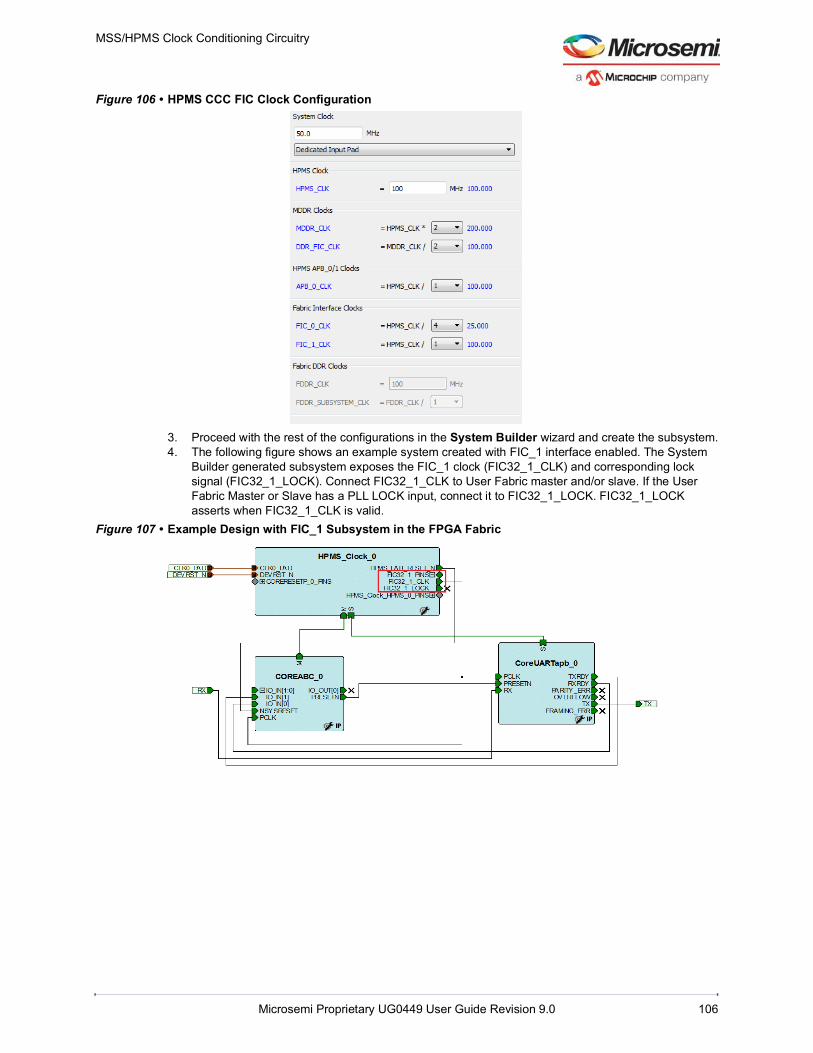
MSS/HPMS Clock Conditioning Circuitry
Microsemi Proprietary UG0449 User Guide Revision 9.0 106
Figure 106 • HPMS CCC FIC Clock Configuration
3. Proceed with the rest of the configurations in the System Builder wizard and create the subsystem.4. The following figure shows an example system created with FIC_1 interface enabled. The System
Builder generated subsystem exposes the FIC_1 clock (FIC32_1_CLK) and corresponding lock signal (FIC32_1_LOCK). Connect FIC32_1_CLK to User Fabric master and/or slave. If the User Fabric Master or Slave has a PLL LOCK input, connect it to FIC32_1_LOCK. FIC32_1_LOCK asserts when FIC32_1_CLK is valid.
Figure 107 • Example Design with FIC_1 Subsystem in the FPGA Fabric

MSS/HPMS Clock Conditioning Circuitry
Microsemi Proprietary UG0449 User Guide Revision 9.0 107
6.7 SYSREG Control RegistersThe following tables list the SYSREG control registers related to MSS CCC and HPMS CCC configuration The base address of the SYSREG control registers is 0x40038000. See the “System Registers Block” chapter of the UG0331: SmartFusion2 Microcontroller Subsystem User Guide or UG0448: IGLOO2 FPGA High Performance Memory Subsystem User Guide for detailed bit definitions of these registers. These system registers should not be modified during run-time, but only configured statically at start-up by flash configuration bits set by the MSS_CCC configurator or IGLOO2 System Builder. A master can read these registers to know the current configuration of the MSS CCC or HPMS CCC or status of the PLLs.
Table 56 • MSS CCC Configuration Registers in SYSREG Block
Register NameAddress Offset
Register Type
Flash Write Protect Reset Source Description
MSSDDR_FACC1_CR 0x98 RW-P Field CC_RESET_N FACC configuration register 1
MSSDDR_FACC2_CR 0x9C RW-P Field CC_RESET_N FACC configuration register 2
Table 57 • HPMS CCC Configuration Registers in SYSREG Block
Register NameAddress Offset
Register Type
Flash Write Protect Reset Source Description
HPMS_FACC1_CR 0x98 RW-P Field CC_RESET_N FACC configuration register 1
HPMS_FACC2_CR 0x9C RW-P Field CC_RESET_N FACC configuration register 2