Embed Size (px)
Citation preview
IGLOO2System Builder User’s Guide
Revision 7 2
Table of Contents
Introduction . . . . . . . . . . . . . . . . . . . . . . . . . . . . . . . . . . . . . . . . . . . . . . . . . . . . . . . . . . . . . . . . . . . . . . 3
1 Accessing System Builder . . . . . . . . . . . . . . . . . . . . . . . . . . . . . . . . . . . . . . . . . . . . . . . . . . . . . . . . . . . 5
2 System Builder Configuration Pages . . . . . . . . . . . . . . . . . . . . . . . . . . . . . . . . . . . . . . . . . . . . . . . . . . . 7Device Features Page . . . . . . . . . . . . . . . . . . . . . . . . . . . . . . . . . . . . . . . . . . . . . . . . . . . . . . . . . . . . . . . . . . . . . . . 7
Memories Page . . . . . . . . . . . . . . . . . . . . . . . . . . . . . . . . . . . . . . . . . . . . . . . . . . . . . . . . . . . . . . . . . . . . . . . . . . . . 9
Peripherals Page . . . . . . . . . . . . . . . . . . . . . . . . . . . . . . . . . . . . . . . . . . . . . . . . . . . . . . . . . . . . . . . . . . . . . . . . . . 14
Clocks Page . . . . . . . . . . . . . . . . . . . . . . . . . . . . . . . . . . . . . . . . . . . . . . . . . . . . . . . . . . . . . . . . . . . . . . . . . . . . . . 23
HPMS Options Page . . . . . . . . . . . . . . . . . . . . . . . . . . . . . . . . . . . . . . . . . . . . . . . . . . . . . . . . . . . . . . . . . . . . . . . 26
SECDED Page . . . . . . . . . . . . . . . . . . . . . . . . . . . . . . . . . . . . . . . . . . . . . . . . . . . . . . . . . . . . . . . . . . . . . . . . . . . . 28
Security Page . . . . . . . . . . . . . . . . . . . . . . . . . . . . . . . . . . . . . . . . . . . . . . . . . . . . . . . . . . . . . . . . . . . . . . . . . . . . . 29
Memory Map Page . . . . . . . . . . . . . . . . . . . . . . . . . . . . . . . . . . . . . . . . . . . . . . . . . . . . . . . . . . . . . . . . . . . . . . . . . 30
3 Fabric Interface Controllers (FICs) and Subsystems . . . . . . . . . . . . . . . . . . . . . . . . . . . . . . . . . . . . . . 33System Builder Reset and Miscellaneous Pins . . . . . . . . . . . . . . . . . . . . . . . . . . . . . . . . . . . . . . . . . . . . . . . . . . . 48
4 Generated System . . . . . . . . . . . . . . . . . . . . . . . . . . . . . . . . . . . . . . . . . . . . . . . . . . . . . . . . . . . . . . . . 50
5 Modifying/Inspecting Your System Builder Design. . . . . . . . . . . . . . . . . . . . . . . . . . . . . . . . . . . . . . . . 52Opening a System Builder Block as SmartDesign . . . . . . . . . . . . . . . . . . . . . . . . . . . . . . . . . . . . . . . . . . . . . . . . . 53
HPMS Configurator . . . . . . . . . . . . . . . . . . . . . . . . . . . . . . . . . . . . . . . . . . . . . . . . . . . . . . . . . . . . . . . . . . . . . . . . 55
Finishing Your Design . . . . . . . . . . . . . . . . . . . . . . . . . . . . . . . . . . . . . . . . . . . . . . . . . . . . . . . . . . . . . . . . . . . . . . 62
A Use Cases . . . . . . . . . . . . . . . . . . . . . . . . . . . . . . . . . . . . . . . . . . . . . . . . . . . . . . . . . . . . . . . . . . . . . . 63
B Product Support . . . . . . . . . . . . . . . . . . . . . . . . . . . . . . . . . . . . . . . . . . . . . . . . . . . . . . . . . . . . . . . . . . 85Customer Service . . . . . . . . . . . . . . . . . . . . . . . . . . . . . . . . . . . . . . . . . . . . . . . . . . . . . . . . . . . . . . . . . . . . . . . . . 85
Customer Technical Support Center . . . . . . . . . . . . . . . . . . . . . . . . . . . . . . . . . . . . . . . . . . . . . . . . . . . . . . . . . . . 85
Technical Support . . . . . . . . . . . . . . . . . . . . . . . . . . . . . . . . . . . . . . . . . . . . . . . . . . . . . . . . . . . . . . . . . . . . . . . . . 85
Website . . . . . . . . . . . . . . . . . . . . . . . . . . . . . . . . . . . . . . . . . . . . . . . . . . . . . . . . . . . . . . . . . . . . . . . . . . . . . . . . . 85
Contacting the Customer Technical Support Center . . . . . . . . . . . . . . . . . . . . . . . . . . . . . . . . . . . . . . . . . . . . . . . 85
ITAR Technical Support . . . . . . . . . . . . . . . . . . . . . . . . . . . . . . . . . . . . . . . . . . . . . . . . . . . . . . . . . . . . . . . . . . . . . 86
Introduction
System Builder is a graphical design wizard designed to help you take advantage of the silicon features of the IGLOO2 device to build a correct-by-design block. System Builder takes you through the following steps:
• Selecting device features for your design
• Creating AMBA-based sub-systems that connect to the IGLOO2 HPMS Fabric Interface Controllers (FICs)
• Setting required configuration options for each selected feature
• Building a correct-by-design complete system
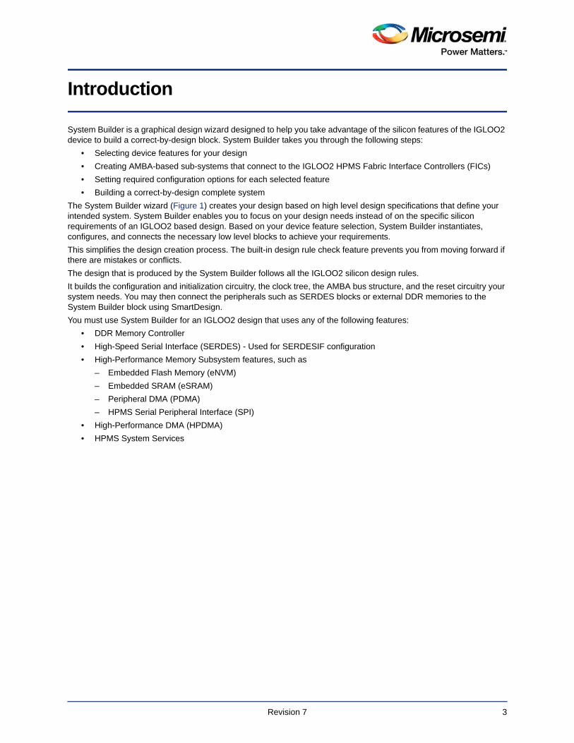
The System Builder wizard (Figure 1) creates your design based on high level design specifications that define your intended system. System Builder enables you to focus on your design needs instead of on the specific silicon requirements of an IGLOO2 based design. Based on your device feature selection, System Builder instantiates, configures, and connects the necessary low level blocks to achieve your requirements.
This simplifies the design creation process. The built-in design rule check feature prevents you from moving forward if there are mistakes or conflicts.
The design that is produced by the System Builder follows all the IGLOO2 silicon design rules.
It builds the configuration and initialization circuitry, the clock tree, the AMBA bus structure, and the reset circuitry your system needs. You may then connect the peripherals such as SERDES blocks or external DDR memories to the System Builder block using SmartDesign.
You must use System Builder for an IGLOO2 design that uses any of the following features:
• DDR Memory Controller
• High-Speed Serial Interface (SERDES) - Used for SERDESIF configuration
• High-Performance Memory Subsystem features, such as
– Embedded Flash Memory (eNVM)
– Embedded SRAM (eSRAM)
– Peripheral DMA (PDMA)
– HPMS Serial Peripheral Interface (SPI)
• High-Performance DMA (HPDMA)
• HPMS System Services
Revision 7 3

Figure 1 • IGLOO2 System Builder
Revision 7 4
1 – Accessing System Builder
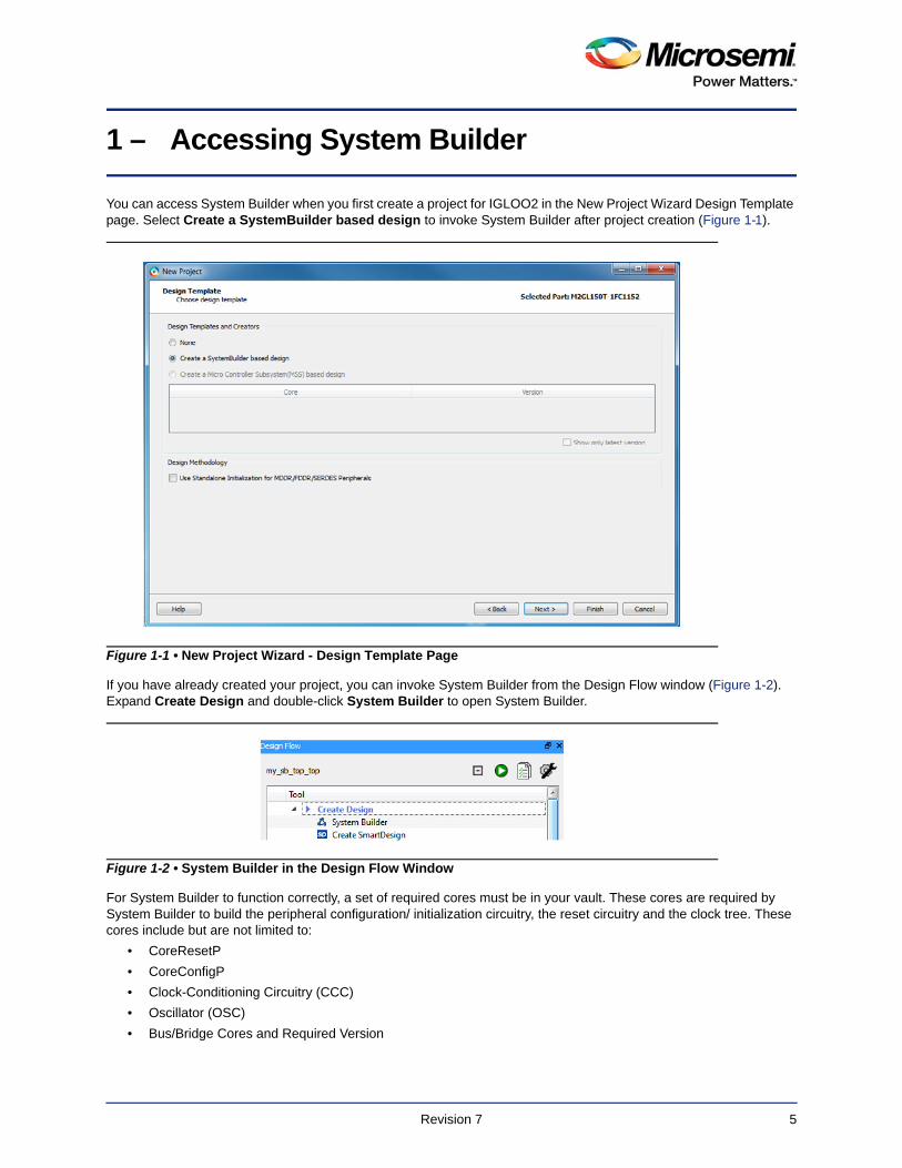
You can access System Builder when you first create a project for IGLOO2 in the New Project Wizard Design Template page. Select Create a SystemBuilder based design to invoke System Builder after project creation (Figure 1-1).
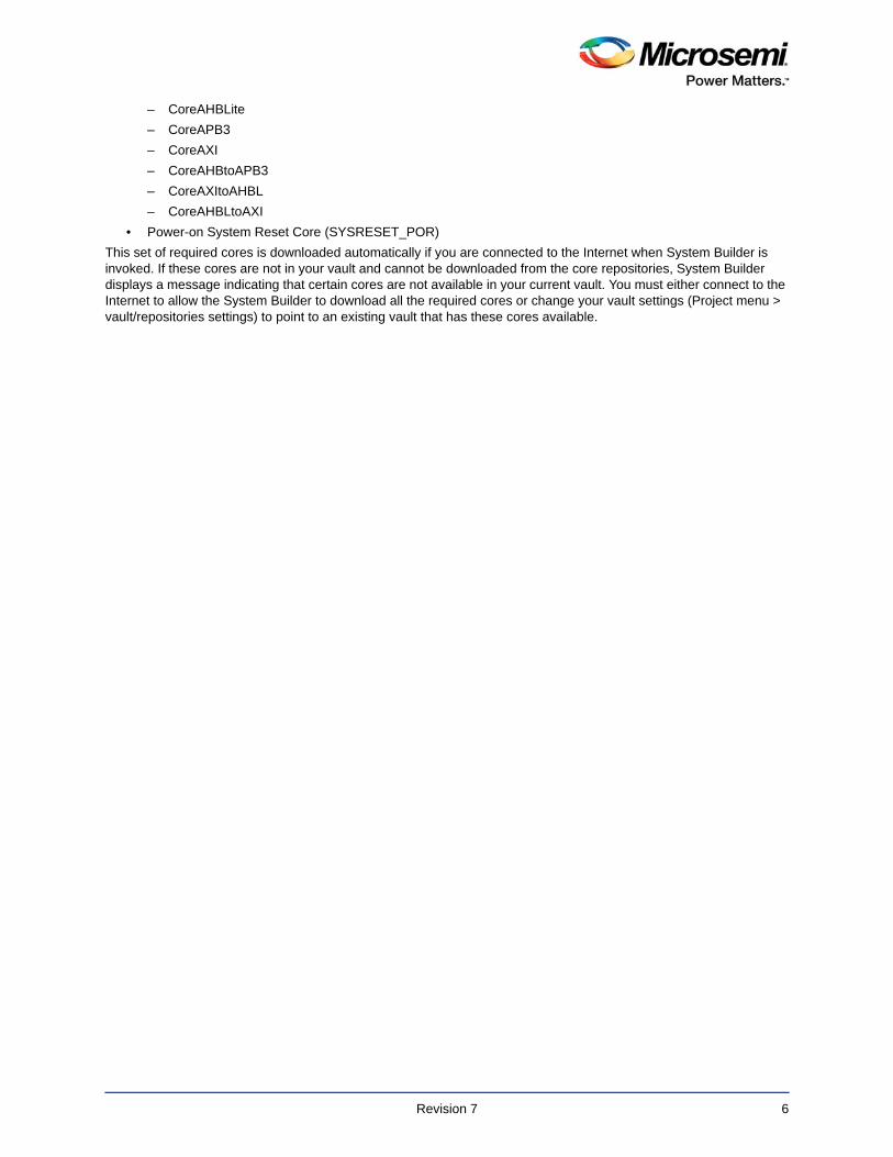
If you have already created your project, you can invoke System Builder from the Design Flow window (Figure 1-2). Expand Create Design and double-click System Builder to open System Builder.
For System Builder to function correctly, a set of required cores must be in your vault. These cores are required by System Builder to build the peripheral configuration/ initialization circuitry, the reset circuitry and the clock tree. These cores include but are not limited to:
• CoreResetP
• CoreConfigP
• Clock-Conditioning Circuitry (CCC)
• Oscillator (OSC)
• Bus/Bridge Cores and Required Version
Figure 1-1 • New Project Wizard - Design Template Page
Figure 1-2 • System Builder in the Design Flow Window
Revision 7 5
– CoreAHBLite
– CoreAPB3
– CoreAXI
– CoreAHBtoAPB3
– CoreAXItoAHBL
– CoreAHBLtoAXI
• Power-on System Reset Core (SYSRESET_POR)
This set of required cores is downloaded automatically if you are connected to the Internet when System Builder is invoked. If these cores are not in your vault and cannot be downloaded from the core repositories, System Builder displays a message indicating that certain cores are not available in your current vault. You must either connect to the Internet to allow the System Builder to download all the required cores or change your vault settings (Project menu > vault/repositories settings) to point to an existing vault that has these cores available.
Revision 7 6
2 – System Builder Configuration Pages
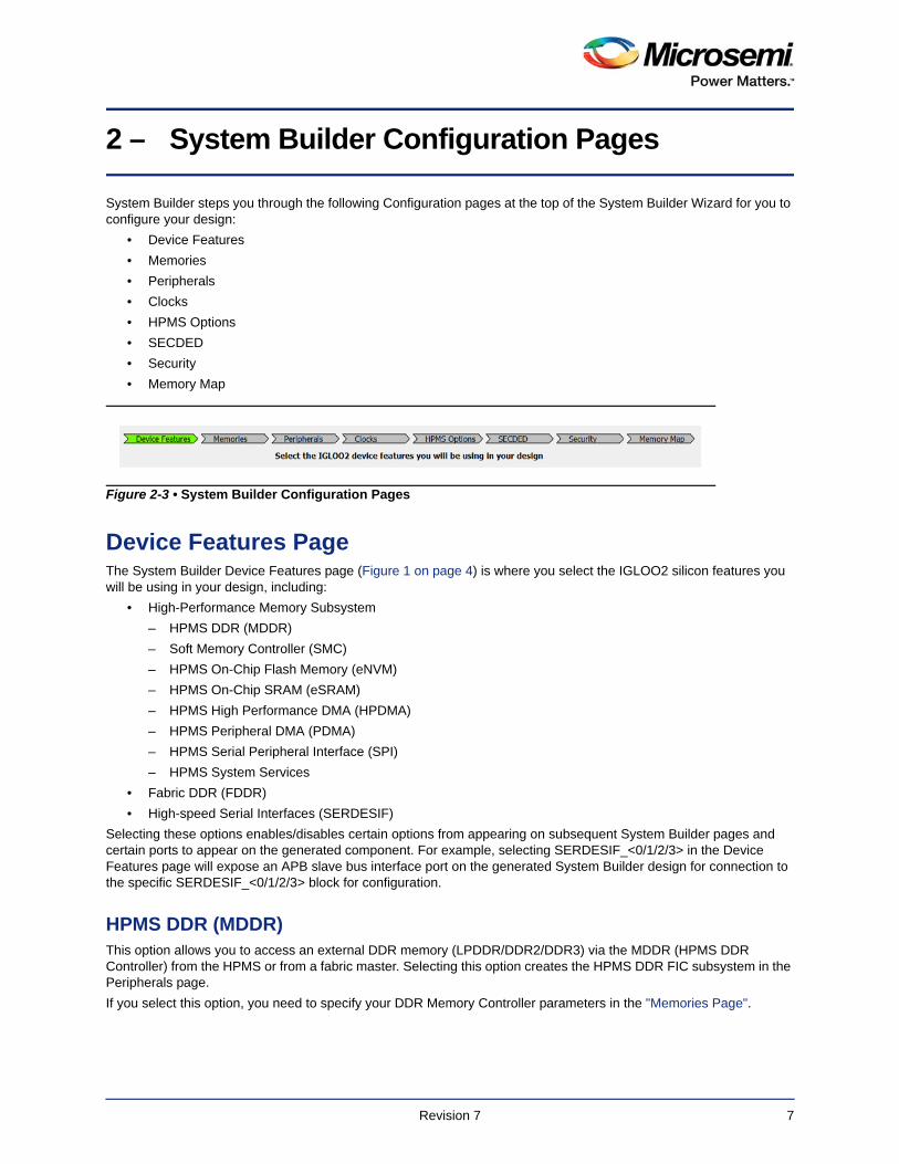
System Builder steps you through the following Configuration pages at the top of the System Builder Wizard for you to configure your design:
• Device Features
• Memories
• Peripherals
• Clocks
• HPMS Options
• SECDED
• Security
• Memory Map
Device Features PageThe System Builder Device Features page (Figure 1 on page 4) is where you select the IGLOO2 silicon features you will be using in your design, including:
• High-Performance Memory Subsystem
– HPMS DDR (MDDR)
– Soft Memory Controller (SMC)
– HPMS On-Chip Flash Memory (eNVM)
– HPMS On-Chip SRAM (eSRAM)
– HPMS High Performance DMA (HPDMA)
– HPMS Peripheral DMA (PDMA)
– HPMS Serial Peripheral Interface (SPI)
– HPMS System Services
• Fabric DDR (FDDR)
• High-speed Serial Interfaces (SERDESIF)
Selecting these options enables/disables certain options from appearing on subsequent System Builder pages and certain ports to appear on the generated component. For example, selecting SERDESIF_<0/1/2/3> in the Device Features page will expose an APB slave bus interface port on the generated System Builder design for connection to the specific SERDESIF_<0/1/2/3> block for configuration.
HPMS DDR (MDDR)This option allows you to access an external DDR memory (LPDDR/DDR2/DDR3) via the MDDR (HPMS DDR Controller) from the HPMS or from a fabric master. Selecting this option creates the HPMS DDR FIC subsystem in the Peripherals page.
If you select this option, you need to specify your DDR Memory Controller parameters in the "Memories Page".
Figure 2-3 • System Builder Configuration Pages
Revision 7 7
Fabric DDR (FDDR)This option allows access to an external DDR Memory (LPDDR/DDR2/DDR3) via the FDDR (Fabric DDR Controller). Selecting this option creates the Fabric DDR subsystem in the Peripherals page. Select this option when you want to use the Fabric DDR controller (FDDR) to access an external DDR memory from a master in the FPGA Fabric.
If you select this option, you need to specify your FDDR Memory Controller parameters in the "Memories Page".
Soft Memory Controller (SMC)This option allows the HPMS to access a Soft Memory Controller in the Fabric. A Soft Memory Controller (CORE_SDR_AXI) is automatically instantiated in the Fabric to control a Single Data Rate external memory (SDR RAM). You may want to select this option if you have a non-DDR based external memory that you want to interface to. When this option is selected, the HPMS SMC FIC Subsystem appears in the Peripherals page.
Selecting this option enables the SMC_FIC Interface mastered by the HPMS. System Builder exposes the HPMS_SMC pins at the top level for you to connect to an external SDR RAM. You can then initiate HPDMA transfers from/to an external SDR RAM using this interface.
Note: You can select either MDDR or SMC but not both; this is a silicon limitation.
HPMS On-Chip Flash Memory (eNVM)Enable this option if you want to use the on-chip Flash Memory (eNVM) to store a data or serialization client. Data storage clients are typically used to store data such as DSP coefficients. Serialization clients are used to add unique device information during programming. If you select this option, you need to configure your eNVM memory parameters in the "Memories Page".
In addition, a bus interface port for a Fabric Master is exposed on the System Builder block. You can connect your Fabric AMBA Master to this port to access the eNVM.
HPMS On-Chip SRAM (eSRAM)Enabling this option exposes a bus interface port for a Fabric Master on the System Builder block. You can connect your Fabric AMBA Master to this port to access the eSRAM.
HPMS High-Performance DMA (HPDMA)The IGLOO2 High-Performance DMA module enables you to initiate transfers between the HPMS DDR/SMC_FIC at one end and eSRAM/eNVM (read only)/Fabric Slaves at the other end. This option exposes a bus interface port for a Fabric Master that is used to configure the HPDMA transfers. You must connect your Fabric AMBA Master or the CoreHPDMACtrl soft IP core (from the IP Catalog) to this port to access the HPDMA configuration registers. For details, refer to the IGLOO2 Silicon User’s Guide.
Note: If you want a Fabric peripheral to participate in HPDMA transfers, you must make sure to add a Fabric AMBA Slave to one of HPMS FIC_0/1 - HPMS Master Subsystems on the System Builder Peripherals page, and configure the AMBA interface type of the slave (AHBLite/APB3/AXI). After System Builder completes generation, a slave bus interface with the configured AMBA interface type is exposed on the System Builder block. Connect your fabric peripheral to this interface.
If you use the Soft Memory Controller (SMC), the HPDMA will be automatically selected.
If the HPDMA is enabled and checked in the Device Features page, the HPDMA block is automatically brought out of reset at Power Up.
HPMS Peripheral DMA (PDMA)The IGLOO2 Peripheral DMA module allows you to initiate transfers between any of the following HPMS/Fabric peripherals:
• eNVM (Read only)
• eSRAM
• Fabric Peripherals
Revision 7 8
This option exposes a bus interface port for a Fabric Master on the System Builder block. You must connect your Fabric AMBA Master to this port to access the PDMA configuration registers. For details, refer to the IGLOO2 Silicon User’s Guide.
Note: If you want a Fabric peripheral to participate in PDMA transfers, you must make sure to add a Fabric AMBA Slave to one of HPMS FIC_0/1 - HPMS Master Subsystems on the System Builder Peripherals page, and configure the AMBA interface type of the slave (AHBLite/APB3/AXI). After System Builder completes generation, a slave bus interface with the configured AMBA interface type is exposed on the System Builder block. Connect your fabric peripheral to this interface.
HPMS Serial Peripheral Interface (SPI)This option enables the HPMS SPI. You can access an external flash memory using this interface. Selecting this option exposes a bus interface port for a Fabric Master. You must connect your Fabric AMBA Master to this port to access the HPMS SPI configuration registers. For details, refer to the IGLOO2 FPGA High Performance Memory Subsystem User's Guide.
HPMS System ServicesThe IGLOO2 HPMS offers you a variety of System Services, including Random Number Generation, Encryption and Flash*Freeze. To enable these services, you must:
1. Check the HPMS System Services checkbox in the Device Features page in System Builder. This exposes the HPMS_FIC_0_SYS_SERVICES_MASTER Bus Interface port on the System Builder generated block.
2. In SmartDesign, instantiate and configure the CoreSysServices soft IP core (available in the IP Catalog) and connect it to this exposed bus interface port.
High Speed Serial InterfacesDepending on the device you have selected for your Libero project, you may have zero to four SERDESIF blocks available for your system. Use the check box to select which SERDESIF blocks you will be using in your design. System Builder does not instantiate the SERDESIF blocks in the generated design but exposes the APB configuration interfaces for each selected SERDESIF block. Use SmartDesign to instantiate and configure the SERDESIF block at the top level of your design and connect it to the appropriate ports in System Builder. For details, refer to the SmartFusion2 and IGLOO2 High Speed Serial Interface Configuration User’s Guide.
Libero automatically stores SERDESIF configuration data from the SERDESIF Configurator in the eNVM. Upon system reset, this configuration data is automatically copied into the appropriate configuration registers of the SERDESIF over the APB connection from the System Builder component to the SERDESIF module.
Refer to the IGLOO2 and SmartFusion2 High Speed Serial Interfaces User Guide for a complete description of all the SERDES options and registers.
Memories PageIf your design uses external DDR memories (LPDDR/DDR2/DDR3) or you want to use the on-board flash memory (eNVM) for data storage or serialization clients, this is where you configure the MDDR/FDDR memory controllers (to work with your external DDR memory) and/or the eNVM.
Depending on the features you have selected in the Device Feature (previous) page, the Memories page may have three tabs for you to configure:
• MDDR
• FDDR
• eNVM
Revision 7 9
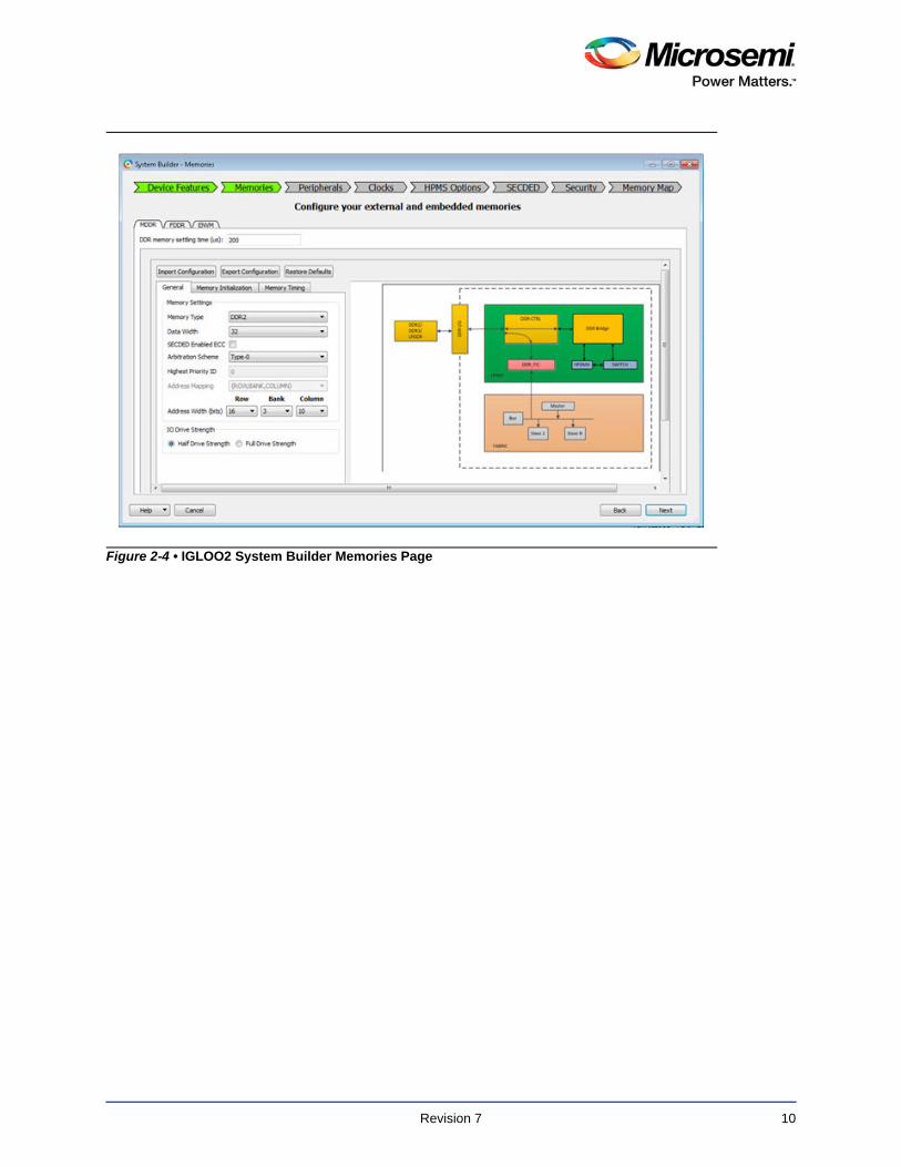
Figure 2-4 • IGLOO2 System Builder Memories Page
Revision 7 10
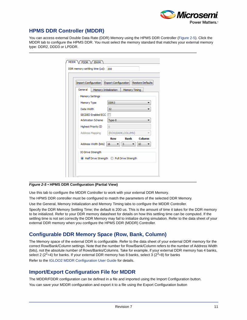
HPMS DDR Controller (MDDR)You can access external Double Data Rate (DDR) Memory using the HPMS DDR Controller (Figure 2-5). Click the MDDR tab to configure the HPMS DDR. You must select the memory standard that matches your external memory type: DDR2, DDD3 or LPDDR.
Use this tab to configure the MDDR Controller to work with your external DDR Memory.
The HPMS DDR controller must be configured to match the parameters of the selected DDR Memory.
Use the General, Memory Initialization and Memory Timing tabs to configure the MDDR Controller.
Specify the DDR Memory Settling Time; the default is 200 us. This is the amount of time it takes for the DDR memory to be initialized. Refer to your DDR memory datasheet for details on how this settling time can be computed. If the settling time is not set correctly the DDR Memory may fail to initialize during simulation. Refer to the data sheet of your external DDR memory when you configure the HPMS DDR (MDDR) Controller.
Configurable DDR Memory Space (Row, Bank, Column)The Memory space of the external DDR is configurable. Refer to the data sheet of your external DDR memory for the correct Row/Bank/Column settings. Note that the number for Row/Bank/Column refers to the number of Address Width (bits), not the absolute number of Rows/Banks/Columns. Take for example, if your external DDR memory has 4 banks, select 2 (22=4) for banks. If your external DDR memory has 8 banks, select 3 (23=8) for banks
Refer to the IGLOO2 MDDR Configuration User Guide for details.
Import/Export Configuration File for MDDRThe MDDR/FDDR configuration can be defined in a file and imported using the Import Configuration button.
You can save your MDDR configuration and export it to a file using the Export Configuration button
Figure 2-5 • HPMS DDR Configuration (Partial View)
Revision 7 11
Libero automatically stores HPMS DDR configuration data (whether entered using the GUI or imported from a file) in the eNVM. Upon system reset, this configuration data is automatically copied into the appropriate configuration registers.
Note: An example DDR configuration file that supports the LPDDR memory used on the IGLOO2 Evaluation Board is available on the board's web page.
Refer to the IGLOO2 DDR Interfaces User's Guide for a complete description of all the DDR configuration options and registers.
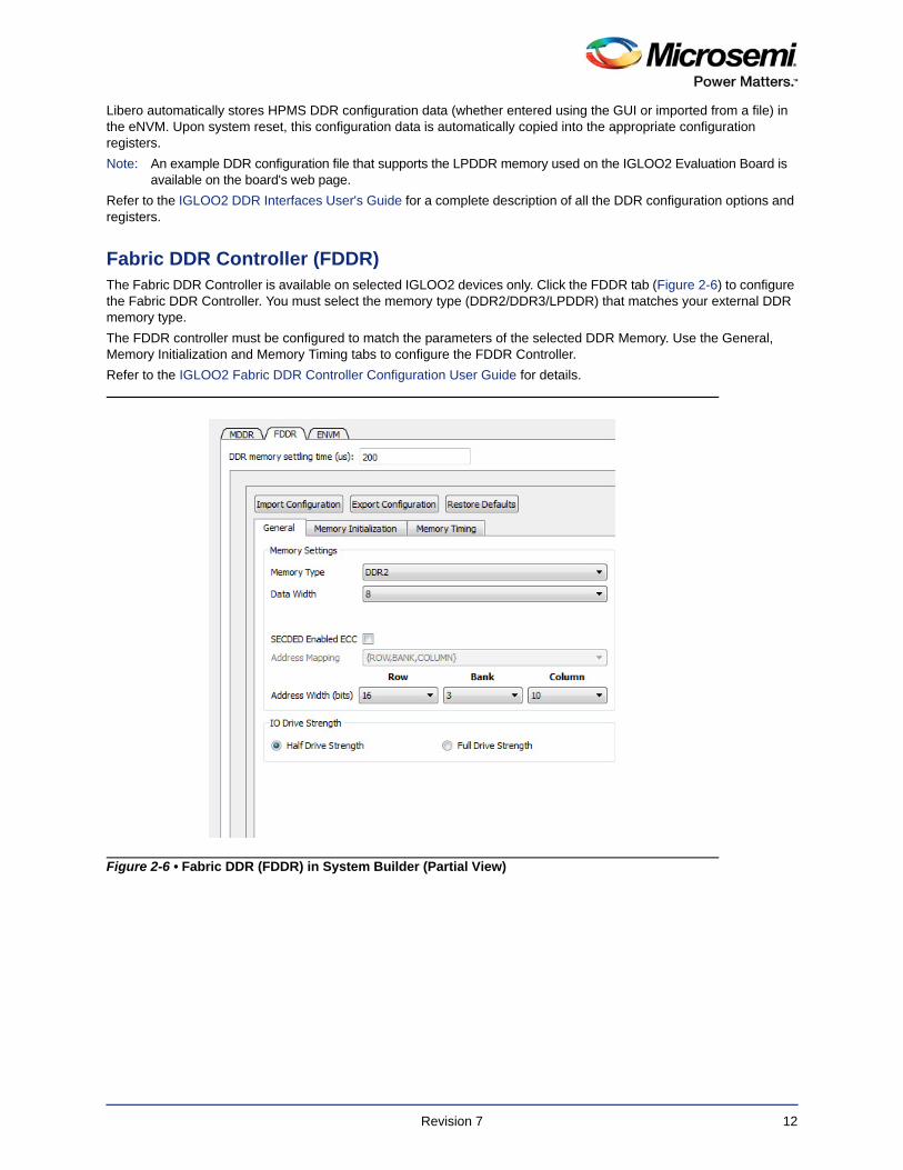
Fabric DDR Controller (FDDR)The Fabric DDR Controller is available on selected IGLOO2 devices only. Click the FDDR tab (Figure 2-6) to configure the Fabric DDR Controller. You must select the memory type (DDR2/DDR3/LPDDR) that matches your external DDR memory type.
The FDDR controller must be configured to match the parameters of the selected DDR Memory. Use the General, Memory Initialization and Memory Timing tabs to configure the FDDR Controller.
Refer to the IGLOO2 Fabric DDR Controller Configuration User Guide for details.
Figure 2-6 • Fabric DDR (FDDR) in System Builder (Partial View)
Revision 7 12
DDR Settling TimeThis is the amount of time it takes for the DDR memory to be initialized. The default value is 200us. Refer to the Data Sheet of your DDR Memory for the correct value to use. Incorrect value may result in the DDR memory's failure to initialize.
Configurable DDR Memory Space (Row, Bank, Column)The Memory space of the external DDR memory is configurable. Refer to the data sheet of your external DDR memory for the correct Row/Bank/Column settings. Note that the number for Row/Bank/Column refers to the Address Width (number of bits), not the absolute number of Rows/Banks/Columns. For example, if your external DDR memory has 4 banks, select 2 (22=4) for banks. If your external DDR memory has 8 banks, select 3 (23=8) for banks.
Import/Export Configuration File for FDDRThe MDDR/FDDR configuration can be defined in a file and imported using the Import Configuration button.
You can save your MDDR/FDDR configuration and export it to a file using the Export Configuration button.
Libero automatically stores the DDR configuration data (whether entered using the GUI or imported from a file) in the eNVM reserved pages. Upon system reset, this configuration data is automatically copied into the appropriate configuration registers.
Note: An example DDR configuration file that supports the LPDDR memory used on the IGLOO2 Evaluation Board is available on the board's web page. Refer to the IGLOO2 DDR Interfaces User's Guide for a complete description of all the DDR configuration options and registers.
Embedded Flash Memory (ENVM)The ENVM tab gives you the option of specifying data storage and Serialization clients in the embedded Non-Volatile Flash Memory (eNVM). Data storage clients are typically used to store data types such as DSP coefficients for instance. Serialization clients are used to add unique device information during programming.
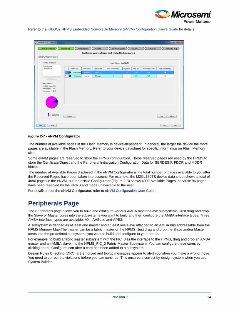
If you want to add data storage or serialization clients to the embedded Flash Memory, select HPMS On-chip Flash Memory (eNVM) on the Device Features page of System Builder. Proceed to the Memories page and click the ENVM tab to configure it. Select the Data Storage or Serialization for the Client type and click Add to System or double-click the client type to add an eNVM client (Figure 2-7). To modify the configuration of your eNVM client, double-click it or select it and click Edit.
Revision 7 13
Refer to the IGLOO2 HPMS Embedded Nonvolatile Memory (eNVM) Configuration User’s Guide for details.
The number of available pages in the Flash Memory is device-dependent. In general, the larger the device the more pages are available in the Flash Memory. Refer to your device datasheet for specific information on Flash Memory size.
Some eNVM pages are reserved to store the HPMS configuration. These reserved pages are used by the HPMS to store the Certificate/Digest and the Peripheral Initialization Configuration Data for SERDESIF, FDDR and MDDR blocks.
The number of Available Pages displayed in the eNVM Configurator is the total number of pages available to you after the Reserved Pages have been taken into account. For example, the M2GL150TS device data sheet shows a total of 4096 pages in the eNVM, but the eNVM Configurator (Figure 2-3) shows 4000 Available Pages, because 96 pages have been reserved by the HPMS and made unavailable to the user.
For details about the eNVM Configurator, refer to eNVM Configuration User Guide.
Peripherals PageThe Peripherals page allows you to build and configure various AMBA master-slave subsystems. Just drag and drop the Slave or Master cores into the subsystems you want to build and then configure the AMBA interface types. Three AMBA interface types are available: AXI, AHBLite and APB3.
A subsystem is defined as at least one master and at least one slave attached to an AMBA bus addressable from the HPMS Memory Map.The master can be a fabric master or the HPMS. Just drag and drop the Slave and/or Master cores into the predefined subsystems you want to build and configure to your needs.
For example, to build a fabric master subsystem with the FIC_0 as the interface to the HPMS, drag and drop an AMBA master and an AMBA slave into the HPMS_FIC_0 Fabric Master Subsystem. You can configure these cores by clicking on the Configure icon after a core has been added to a subsystem.
Design Rules Checking (DRC) are enforced and tooltip messages appear to alert you when you make a wrong move. You need to correct the violations before you can continue. This ensures a correct-by-design system when you use System Builder.
Figure 2-7 • eNVM Configurator
Revision 7 14
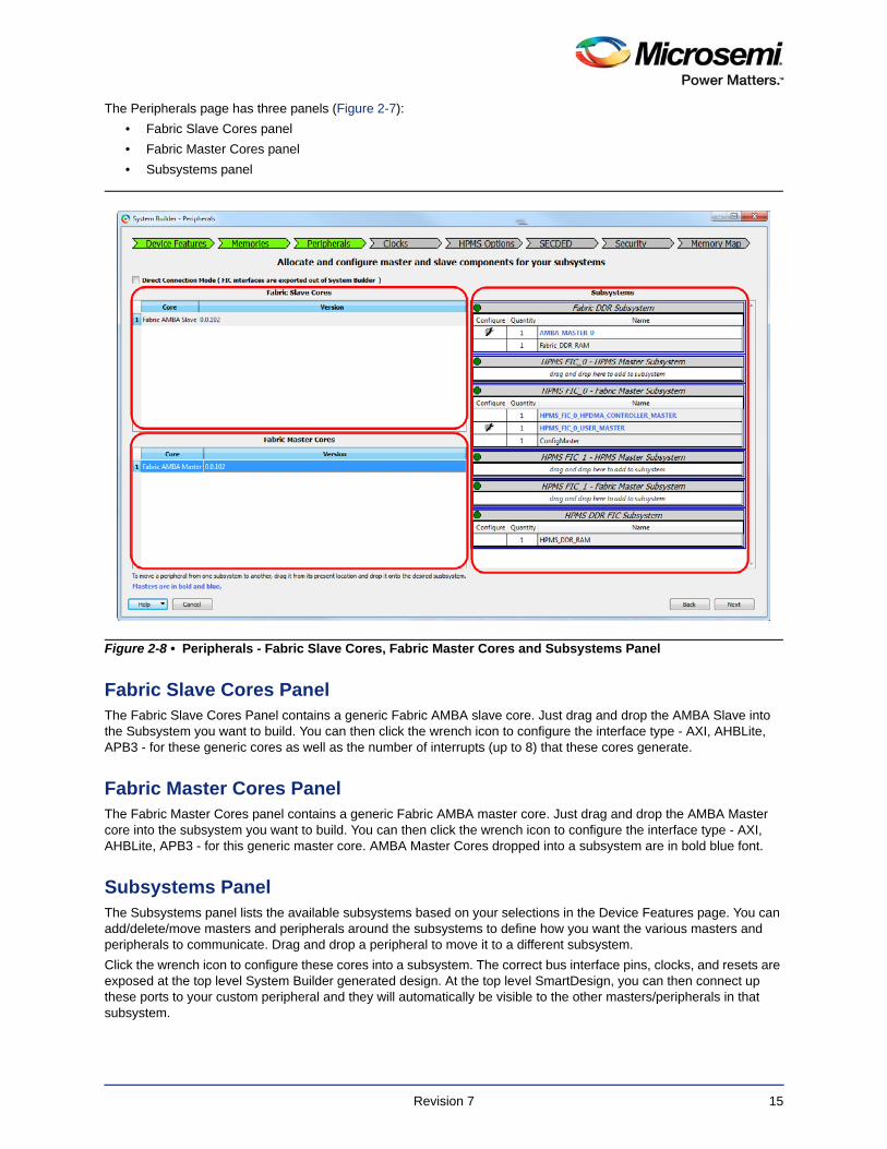
The Peripherals page has three panels (Figure 2-7):
• Fabric Slave Cores panel
• Fabric Master Cores panel
• Subsystems panel
Fabric Slave Cores PanelThe Fabric Slave Cores Panel contains a generic Fabric AMBA slave core. Just drag and drop the AMBA Slave into the Subsystem you want to build. You can then click the wrench icon to configure the interface type - AXI, AHBLite, APB3 - for these generic cores as well as the number of interrupts (up to 8) that these cores generate.
Fabric Master Cores PanelThe Fabric Master Cores panel contains a generic Fabric AMBA master core. Just drag and drop the AMBA Master core into the subsystem you want to build. You can then click the wrench icon to configure the interface type - AXI, AHBLite, APB3 - for this generic master core. AMBA Master Cores dropped into a subsystem are in bold blue font.
Subsystems PanelThe Subsystems panel lists the available subsystems based on your selections in the Device Features page. You can add/delete/move masters and peripherals around the subsystems to define how you want the various masters and peripherals to communicate. Drag and drop a peripheral to move it to a different subsystem.
Click the wrench icon to configure these cores into a subsystem. The correct bus interface pins, clocks, and resets are exposed at the top level System Builder generated design. At the top level SmartDesign, you can then connect up these ports to your custom peripheral and they will automatically be visible to the other masters/peripherals in that subsystem.
Figure 2-8 • Peripherals - Fabric Slave Cores, Fabric Master Cores and Subsystems Panel
Revision 7 15

You can click the wrench icon to configure the options of that core (Figure 2-9). In the configuration dialog, you can specify the AMBA protocol for that core. Not all subsystems support masters/slaves with all AMBA protocols. Details are in Chapter 3, "Fabric Interface Controllers (FICs) and Subsystems". You can also specify the Quantity, which determines how many cores with that configuration will be instantiated in the generated system. You can also rename a peripheral which will be used in the generated port names,
You can choose to delete any peripherals that you may have added to a subsystem. To do so, right-click and choose Delete.
The Peripherals page Subsystem Panel allows you to create a subsystem for each of those FIC interfaces:
• HPMS DDR_FIC Subsystem. The HPMS DDR_FIC is available when you configure the HPMS DDR block (MDDR) such that an external DDR memory can be accessed from an FPGA fabric master via an AXI or AHBLite interface.
• HPMS SMC_FIC Subsystem. The HPMS SMC_FIC is used when you configure the HPMS DDR Block in the Single Date Rate (SDR) mode. In this configuration, the HPMS accesses external Single Data Rate DRAM or Asynchronous memories via a soft memory controller instantiated in the FPGA fabric such as CoreSDR_AXI and CoreSDR_AHB. The HPMS SMC_FIC is an AXI or AHBLite slave AMBA interface. The HPMS DDR_FIC and HPMS SMC_FIC interfaces are mutually exclusive; only one is active at a time depending on your selection in the Device Features page.
• HPMS FIC_0 Fabric Master Subsystem. The HPMS FIC_0 master interface enables you to naturally extend the HPMS AMBA bus into the FPGA fabric.
• HPMS FIC_0 HPMS Master Subsystem. Using this interface you can have the HPMS accessing the fabric.
• HPMS FIC_1 Fabric Master Subsystem. The FIC_1 master interface enables you to naturally extend the HPMS AMBA bus into the FPGA fabric. This interface is available only on larger devices.
• HPMS FIC_1 HPMS Master Subsystem. Using this interface you can have the HPMS accessing the fabric. This interface is available only on larger devices.
• Fabric DDR Subsystem (Available only on larger devices). Use this interface for a fabric DDR Controller subsystem to access fabric DDR_RAM.
Note: The HPMS FIC_2 interface is not available to you, as it is reserved by the System Builder to create the peripheral initialization configuration bus for the SERDES, the MDDR and the FDDR blocks.
Figure 2-9 • Configuring Fabric AMBA Master Core
Revision 7 16
Default Mode and Direct Connection Mode System Builder operates in two modes:
• Normal (Default) Mode - In this mode, System Builder builds the AMBA bus structure (buses and bridges) of the correct AMBA type and attaches the Masters and Slaves to the bus cores based on your configuration and specifications. In addition, System builder also builds the Clock network and the Reset circuitry for every subsystem. The correct bus interface pins, clocks, and resets are exposed at the top level System Builder generated design. This is the default mode.
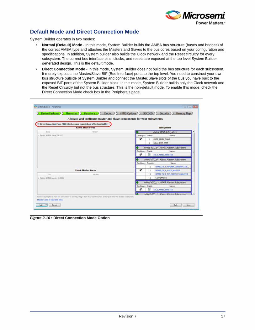
• Direct Connection Mode - In this mode, System Builder does not build the bus structure for each subsystem. It merely exposes the Master/Slave BIF (Bus Interface) ports to the top level. You need to construct your own bus structure outside of System Builder and connect the Master/Slave slots of the Bus you have built to the exposed BIF ports of the System Builder block. In this mode, System Builder builds only the Clock network and the Reset Circuitry but not the bus structure. This is the non-default mode. To enable this mode, check the Direct Connection Mode check box in the Peripherals page.
Figure 2-10 • Direct Connection Mode Option
Revision 7 17
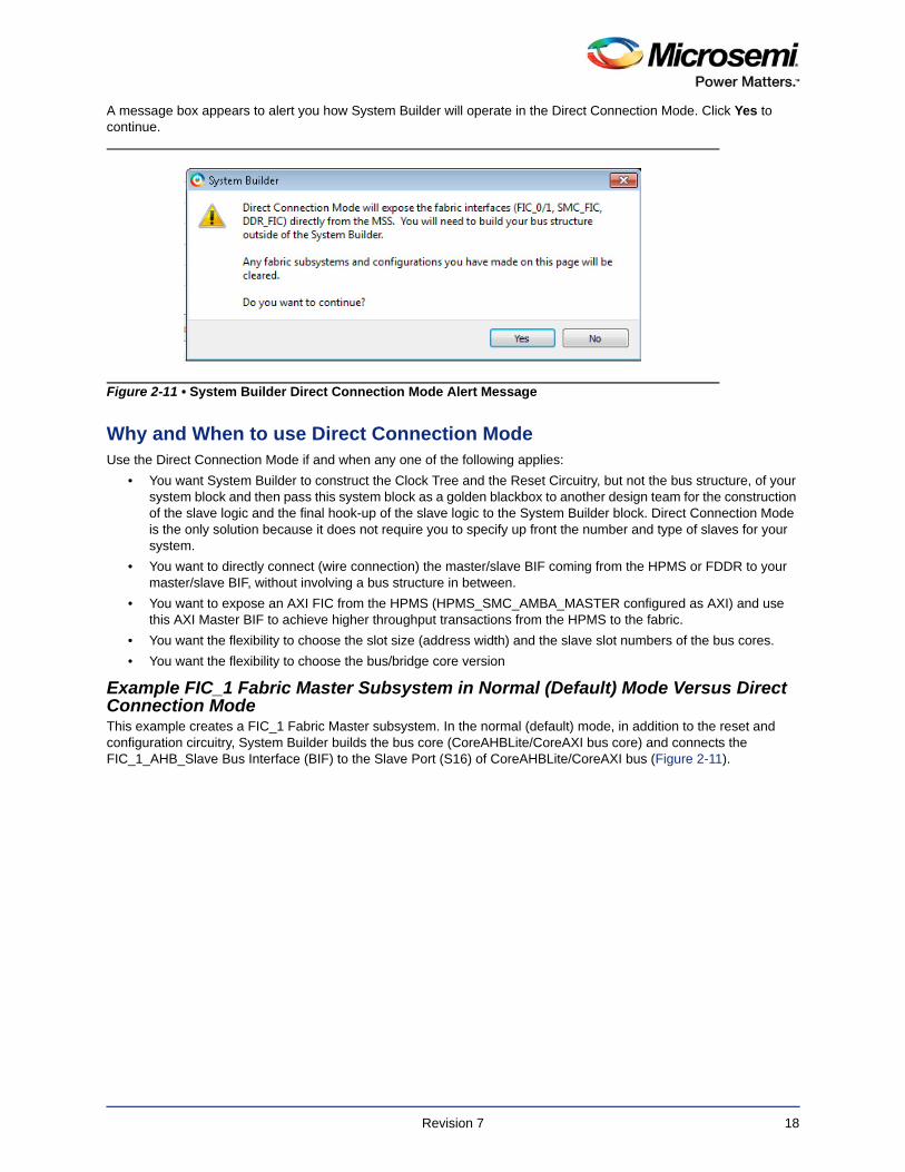
A message box appears to alert you how System Builder will operate in the Direct Connection Mode. Click Yes to continue.
Why and When to use Direct Connection ModeUse the Direct Connection Mode if and when any one of the following applies:
• You want System Builder to construct the Clock Tree and the Reset Circuitry, but not the bus structure, of your system block and then pass this system block as a golden blackbox to another design team for the construction of the slave logic and the final hook-up of the slave logic to the System Builder block. Direct Connection Mode is the only solution because it does not require you to specify up front the number and type of slaves for your system.
• You want to directly connect (wire connection) the master/slave BIF coming from the HPMS or FDDR to your master/slave BIF, without involving a bus structure in between.
• You want to expose an AXI FIC from the HPMS (HPMS_SMC_AMBA_MASTER configured as AXI) and use this AXI Master BIF to achieve higher throughput transactions from the HPMS to the fabric.
• You want the flexibility to choose the slot size (address width) and the slave slot numbers of the bus cores.
• You want the flexibility to choose the bus/bridge core version
Example FIC_1 Fabric Master Subsystem in Normal (Default) Mode Versus Direct Connection Mode This example creates a FIC_1 Fabric Master subsystem. In the normal (default) mode, in addition to the reset and configuration circuitry, System Builder builds the bus core (CoreAHBLite/CoreAXI bus core) and connects the FIC_1_AHB_Slave Bus Interface (BIF) to the Slave Port (S16) of CoreAHBLite/CoreAXI bus (Figure 2-11).
Figure 2-11 • System Builder Direct Connection Mode Alert Message
Revision 7 18
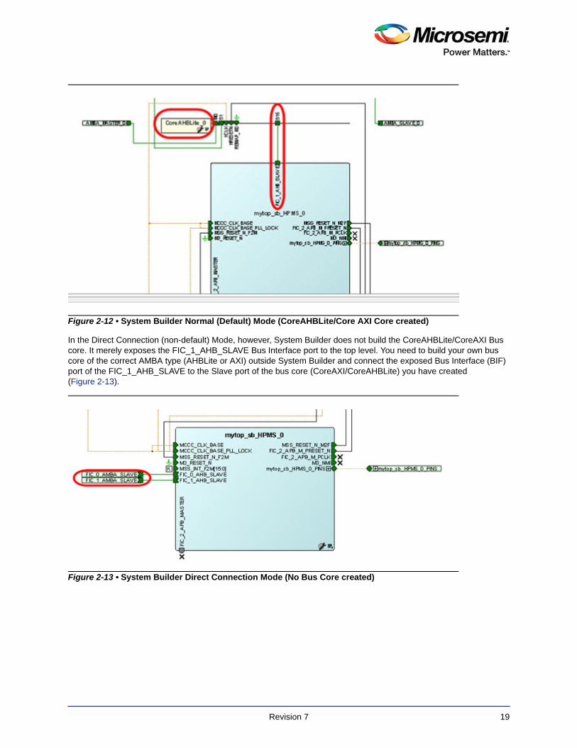
In the Direct Connection (non-default) Mode, however, System Builder does not build the CoreAHBLite/CoreAXI Bus core. It merely exposes the FIC_1_AHB_SLAVE Bus Interface port to the top level. You need to build your own bus core of the correct AMBA type (AHBLite or AXI) outside System Builder and connect the exposed Bus Interface (BIF) port of the FIC_1_AHB_SLAVE to the Slave port of the bus core (CoreAXI/CoreAHBLite) you have created (Figure 2-13).
Figure 2-12 • System Builder Normal (Default) Mode (CoreAHBLite/Core AXI Core created)
Figure 2-13 • System Builder Direct Connection Mode (No Bus Core created)
Revision 7 19
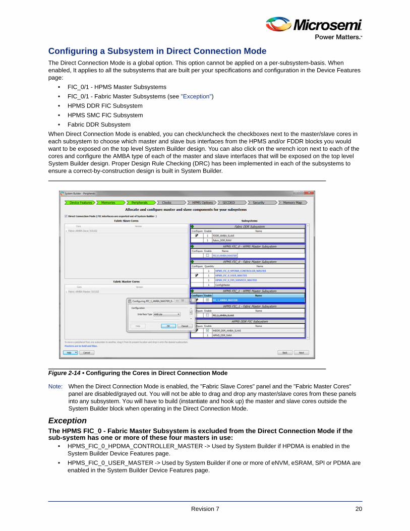
Configuring a Subsystem in Direct Connection ModeThe Direct Connection Mode is a global option. This option cannot be applied on a per-subsystem-basis. When enabled, It applies to all the subsystems that are built per your specifications and configuration in the Device Features page:
• FIC_0/1 - HPMS Master Subsystems
• FIC_0/1 - Fabric Master Subsystems (see "Exception")
• HPMS DDR FIC Subsystem
• HPMS SMC FIC Subsystem
• Fabric DDR Subsystem
When Direct Connection Mode is enabled, you can check/uncheck the checkboxes next to the master/slave cores in each subsystem to choose which master and slave bus interfaces from the HPMS and/or FDDR blocks you would want to be exposed on the top level System Builder design. You can also click on the wrench icon next to each of the cores and configure the AMBA type of each of the master and slave interfaces that will be exposed on the top level System Builder design. Proper Design Rule Checking (DRC) has been implemented in each of the subsystems to ensure a correct-by-construction design is built in System Builder.
Note: When the Direct Connection Mode is enabled, the "Fabric Slave Cores" panel and the "Fabric Master Cores" panel are disabled/grayed out. You will not be able to drag and drop any master/slave cores from these panels into any subsystem. You will have to build (instantiate and hook up) the master and slave cores outside the System Builder block when operating in the Direct Connection Mode.
ExceptionThe HPMS FIC_0 - Fabric Master Subsystem is excluded from the Direct Connection Mode if the sub-system has one or more of these four masters in use:
• HPMS_FIC_0_HPDMA_CONTROLLER_MASTER -> Used by System Builder if HPDMA is enabled in the System Builder Device Features page.
• HPMS_FIC_0_USER_MASTER -> Used by System Builder if one or more of eNVM, eSRAM, SPI or PDMA are enabled in the System Builder Device Features page.
Figure 2-14 • Configuring the Cores in Direct Connection Mode
Revision 7 20
• HPMS_FIC_0_SYS_SERVICES_MASTER -> Used by System Builder if HPMS System Services is enabled in the System Builder Device Features page.
• ConfigMaster -> Used by System Builder if one or more of MDDR, FDDR or SERDESIF blocks are enabled in the System Builder Device Features page.
If one or more of the masters listed above are in use, this subsystem will operate in its normal mode even if Direct Connection Mode is turned ON, and System Builder will build the AMBA bus structure for this subsystem.
If none of the masters listed above are in use, this subsystem also will operate in Direct Connection Mode, if turned ON, like all other subsystems.
Follow-up Actions after Direct Connection ModeIn Direct Connection Mode, the System Builder block exposes to the top level all Master/Slave Bus Interfaces (BIF) corresponding to the subsystems that are enabled as per your specifications and configuration in the Device Features page and the Peripherals page. After System Builder generation completes, you need to:
1. Manually build the correct AMBA-compliant bus-bridge core structure for every subsystem.
2. Connect the master/slave BIF ports exposed on the System Builder block to the appropriate BIF ports of the bus cores.
3. Connect the clock and reset pins of the slave/master and bus cores to the appropriate clock and reset pins of the corresponding subsystem pin groups.
4. Instantiate your actual master and slave cores in the design and connect all their clock, reset and bus interface ports appropriately.
Revision 7 21
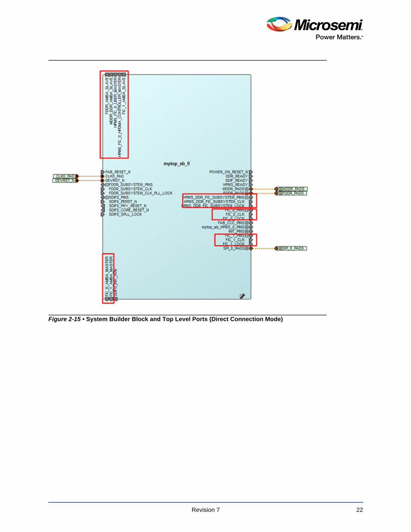
Figure 2-15 • System Builder Block and Top Level Ports (Direct Connection Mode)
Revision 7 22
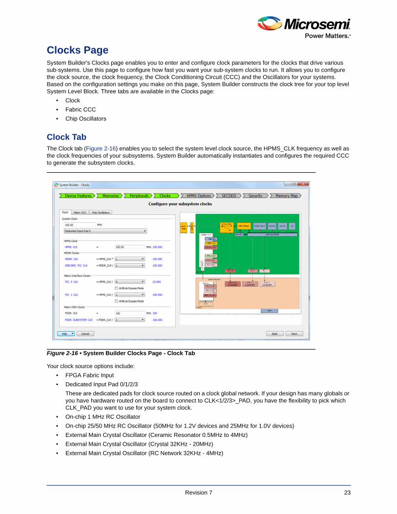
Clocks PageSystem Builder's Clocks page enables you to enter and configure clock parameters for the clocks that drive various sub-systems. Use this page to configure how fast you want your sub-system clocks to run. It allows you to configure the clock source, the clock frequency, the Clock Conditioning Circuit (CCC) and the Oscillators for your systems. Based on the configuration settings you make on this page, System Builder constructs the clock tree for your top level System Level Block. Three tabs are available in the Clocks page:
• Clock
• Fabric CCC
• Chip Oscillators
Clock TabThe Clock tab (Figure 2-16) enables you to select the system level clock source, the HPMS_CLK frequency as well as the clock frequencies of your subsystems. System Builder automatically instantiates and configures the required CCC to generate the subsystem clocks.
Your clock source options include:
• FPGA Fabric Input
• Dedicated Input Pad 0/1/2/3
These are dedicated pads for clock source routed on a clock global network. If your design has many globals or you have hardware routed on the board to connect to CLK<1/2/3>_PAD, you have the flexibility to pick which CLK_PAD you want to use for your system clock.
• On-chip 1 MHz RC Oscillator
• On-chip 25/50 MHz RC Oscillator (50MHz for 1.2V devices and 25MHz for 1.0V devices)
• External Main Crystal Oscillator (Ceramic Resonator 0.5MHz to 4MHz)
• External Main Crystal Oscillator (Crystal 32KHz - 20MHz)
• External Main Crystal Oscillator (RC Network 32KHz - 4MHz)
Figure 2-16 • System Builder Clocks Page - Clock Tab
Revision 7 23
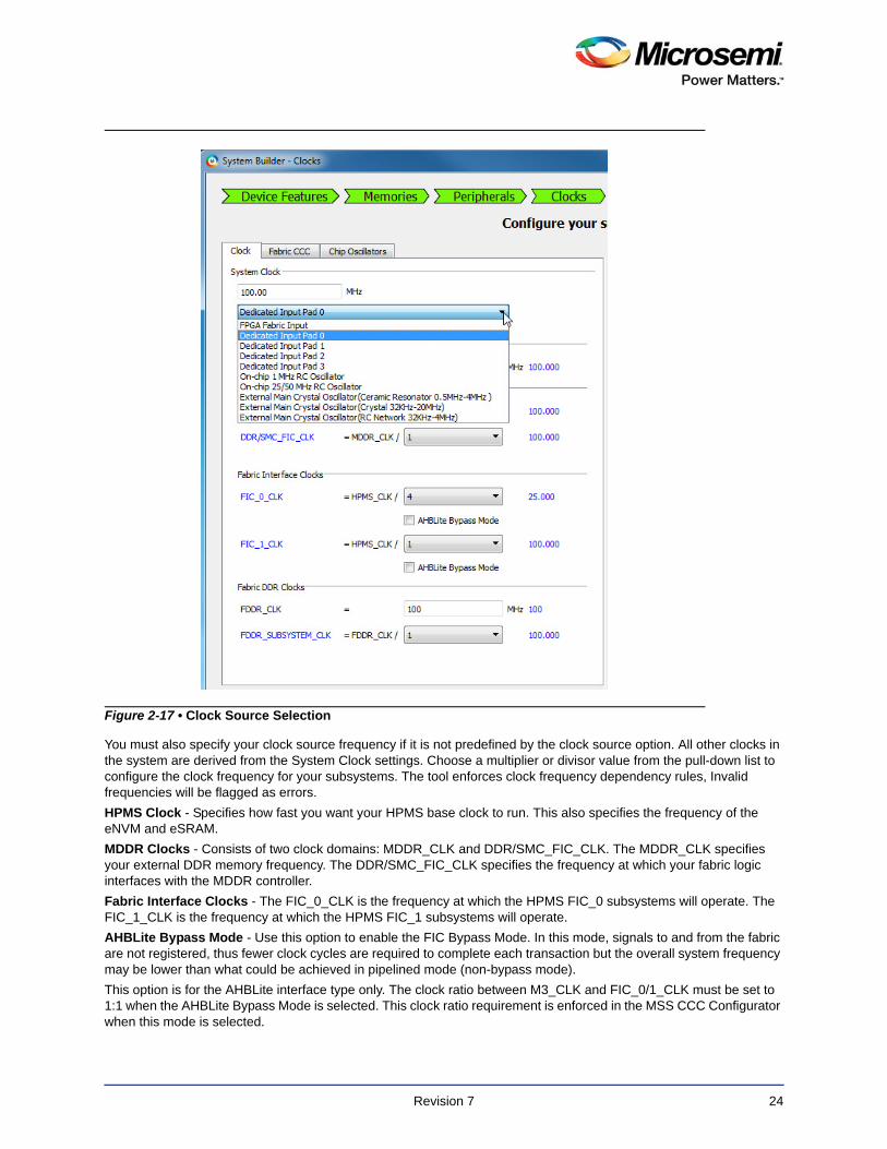
You must also specify your clock source frequency if it is not predefined by the clock source option. All other clocks in the system are derived from the System Clock settings. Choose a multiplier or divisor value from the pull-down list to configure the clock frequency for your subsystems. The tool enforces clock frequency dependency rules, Invalid frequencies will be flagged as errors.
HPMS Clock - Specifies how fast you want your HPMS base clock to run. This also specifies the frequency of the eNVM and eSRAM.
MDDR Clocks - Consists of two clock domains: MDDR_CLK and DDR/SMC_FIC_CLK. The MDDR_CLK specifies your external DDR memory frequency. The DDR/SMC_FIC_CLK specifies the frequency at which your fabric logic interfaces with the MDDR controller.
Fabric Interface Clocks - The FIC_0_CLK is the frequency at which the HPMS FIC_0 subsystems will operate. The FIC_1_CLK is the frequency at which the HPMS FIC_1 subsystems will operate.
AHBLite Bypass Mode - Use this option to enable the FIC Bypass Mode. In this mode, signals to and from the fabric are not registered, thus fewer clock cycles are required to complete each transaction but the overall system frequency may be lower than what could be achieved in pipelined mode (non-bypass mode).
This option is for the AHBLite interface type only. The clock ratio between M3_CLK and FIC_0/1_CLK must be set to 1:1 when the AHBLite Bypass Mode is selected. This clock ratio requirement is enforced in the MSS CCC Configurator when this mode is selected.
Figure 2-17 • Clock Source Selection
Revision 7 24
Fabric DDR Clocks - The FDDR_CLK specifies your external fabric DDR memory frequency. The FDDR_SUBSYSTEM_CLK is the frequency at which your fabric logic interfaces with the Fabric DDR controller.
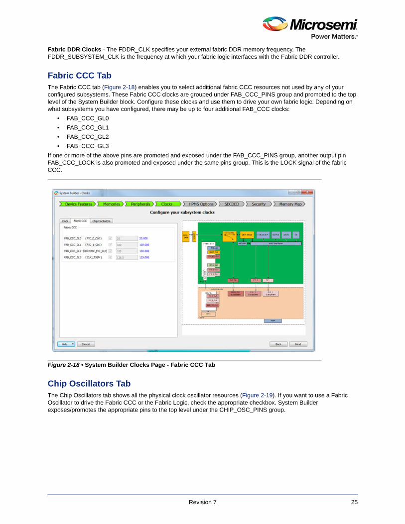
Fabric CCC TabThe Fabric CCC tab (Figure 2-18) enables you to select additional fabric CCC resources not used by any of your configured subsystems. These Fabric CCC clocks are grouped under FAB_CCC_PINS group and promoted to the top level of the System Builder block. Configure these clocks and use them to drive your own fabric logic. Depending on what subsystems you have configured, there may be up to four additional FAB_CCC clocks:
• FAB_CCC_GL0
• FAB_CCC_GL1
• FAB_CCC_GL2
• FAB_CCC_GL3
If one or more of the above pins are promoted and exposed under the FAB_CCC_PINS group, another output pin FAB_CCC_LOCK is also promoted and exposed under the same pins group. This is the LOCK signal of the fabric CCC.
Chip Oscillators TabThe Chip Oscillators tab shows all the physical clock oscillator resources (Figure 2-19). If you want to use a Fabric Oscillator to drive the Fabric CCC or the Fabric Logic, check the appropriate checkbox. System Builder exposes/promotes the appropriate pins to the top level under the CHIP_OSC_PINS group.
Figure 2-18 • System Builder Clocks Page - Fabric CCC Tab
Revision 7 25
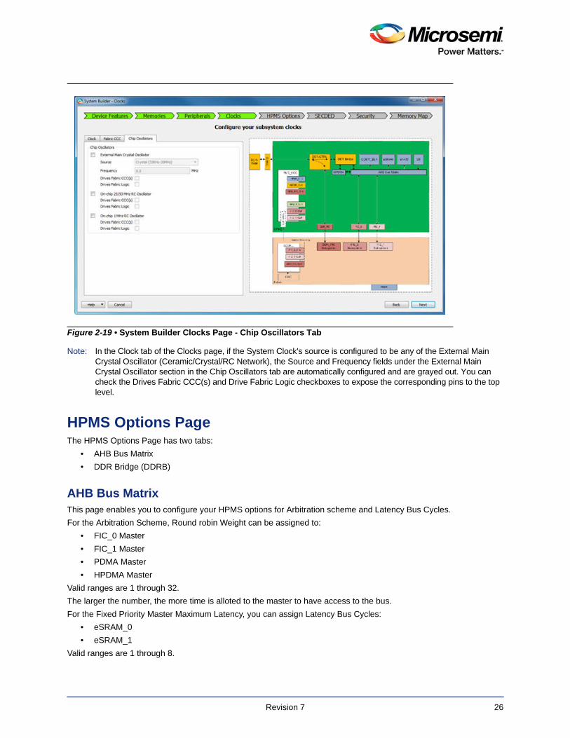
Note: In the Clock tab of the Clocks page, if the System Clock's source is configured to be any of the External Main Crystal Oscillator (Ceramic/Crystal/RC Network), the Source and Frequency fields under the External Main Crystal Oscillator section in the Chip Oscillators tab are automatically configured and are grayed out. You can check the Drives Fabric CCC(s) and Drive Fabric Logic checkboxes to expose the corresponding pins to the top level.
HPMS Options PageThe HPMS Options Page has two tabs:
• AHB Bus Matrix
• DDR Bridge (DDRB)
AHB Bus MatrixThis page enables you to configure your HPMS options for Arbitration scheme and Latency Bus Cycles.
For the Arbitration Scheme, Round robin Weight can be assigned to:
• FIC_0 Master
• FIC_1 Master
• PDMA Master
• HPDMA Master
Valid ranges are 1 through 32.
The larger the number, the more time is alloted to the master to have access to the bus.
For the Fixed Priority Master Maximum Latency, you can assign Latency Bus Cycles:
• eSRAM_0
• eSRAM_1
Valid ranges are 1 through 8.
Figure 2-19 • System Builder Clocks Page - Chip Oscillators Tab
Revision 7 26
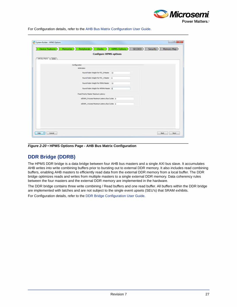
For Configuration details, refer to the AHB Bus Matrix Configuration User Guide.
DDR Bridge (DDRB)The HPMS DDR bridge is a data bridge between four AHB bus masters and a single AXI bus slave. It accumulates AHB writes into write combining buffers prior to bursting out to external DDR memory. It also includes read combining buffers, enabling AHB masters to efficiently read data from the external DDR memory from a local buffer. The DDR bridge optimizes reads and writes from multiple masters to a single external DDR memory. Data coherency rules between the four masters and the external DDR memory are implemented in the hardware.
The DDR bridge contains three write combining / Read buffers and one read buffer. All buffers within the DDR bridge are implemented with latches and are not subject to the single event upsets (SEU's) that SRAM exhibits.
For Configuration details, refer to the DDR Bridge Configuration User Guide.
Figure 2-20 • HPMS Options Page - AHB Bus Matrix Configuration
Revision 7 27
SECDED PageThis page enables you to configure your Single Error Correction/Double Error Detection logic and the conditions under which an interrupt is raised when an error is detected. You may want to use this page to configure your EDAC (Error Detection and Correction) to protect the eSRAMs in your IGLOO2 device and external DDR memories, especially if your application is to be used in radiation prone environments.
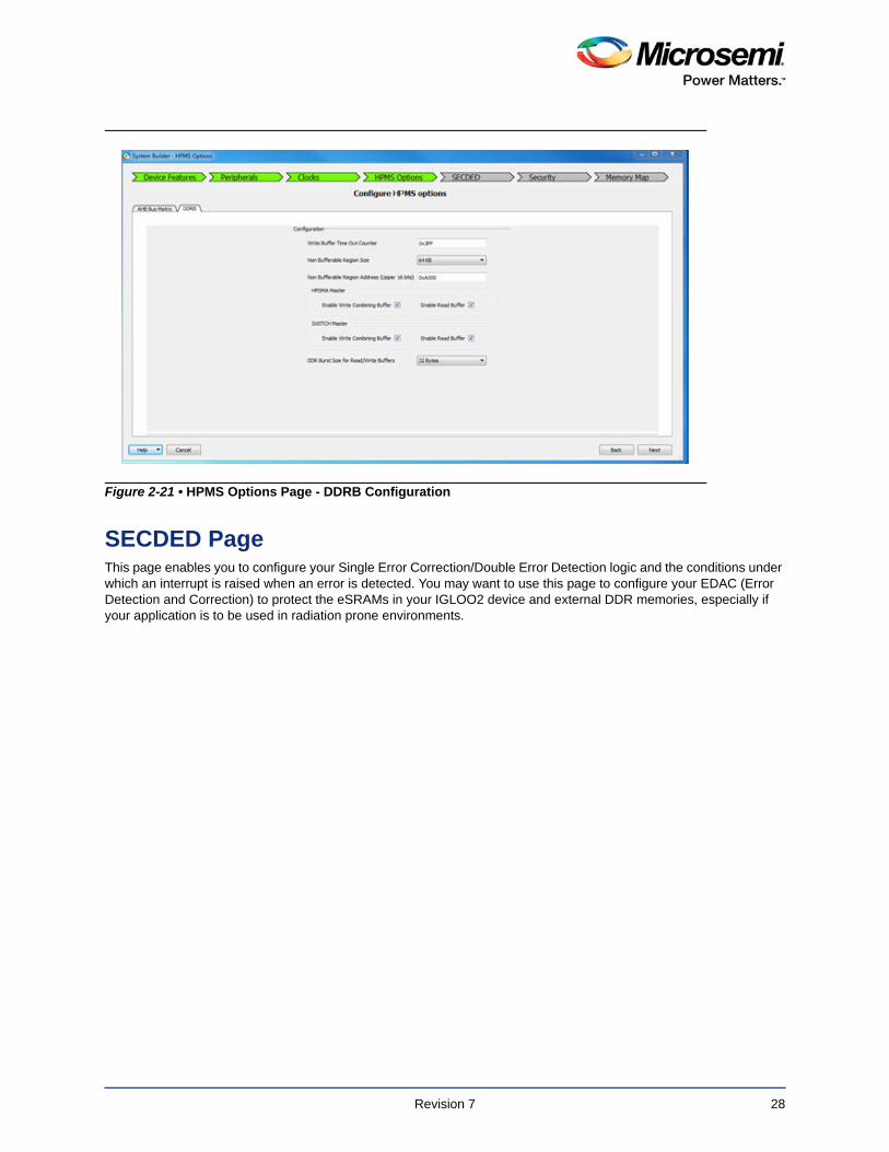
Figure 2-21 • HPMS Options Page - DDRB Configuration
Revision 7 28
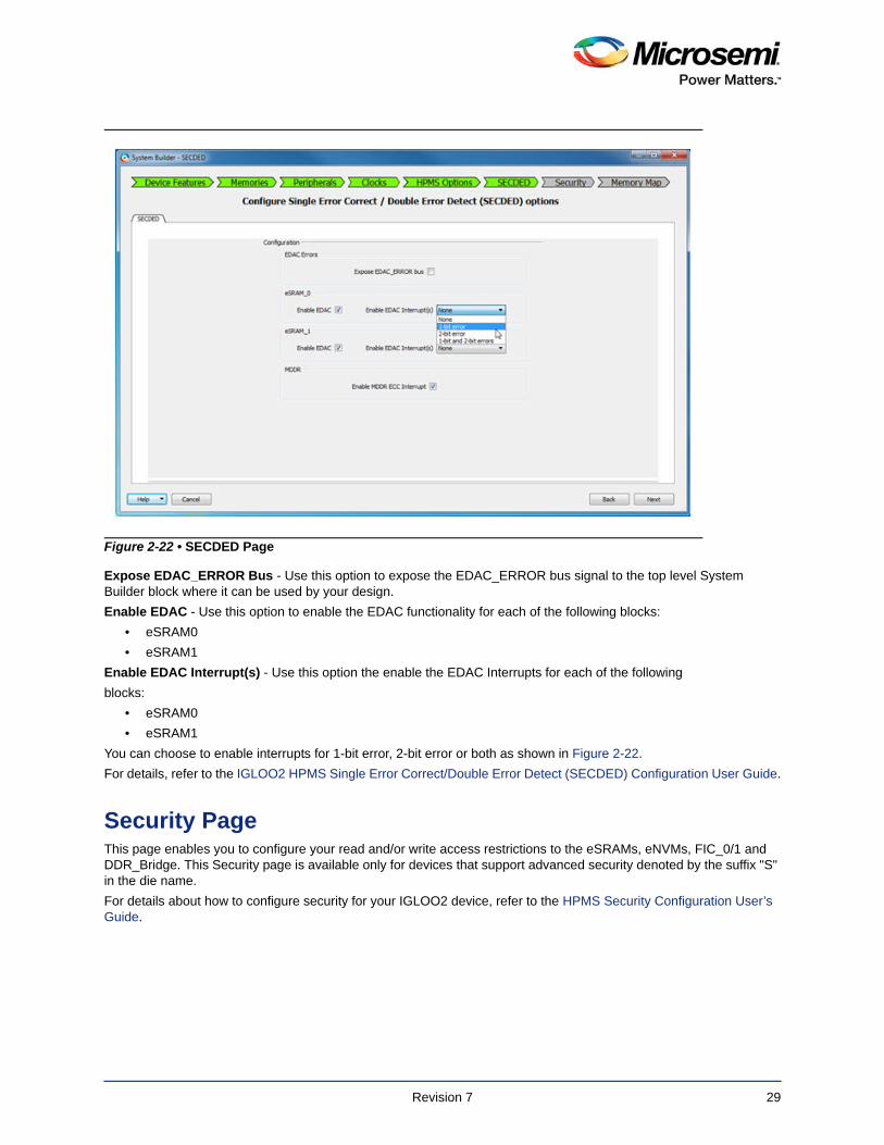
Expose EDAC_ERROR Bus - Use this option to expose the EDAC_ERROR bus signal to the top level System Builder block where it can be used by your design.
Enable EDAC - Use this option to enable the EDAC functionality for each of the following blocks:
• eSRAM0
• eSRAM1
Enable EDAC Interrupt(s) - Use this option the enable the EDAC Interrupts for each of the following
blocks:
• eSRAM0
• eSRAM1
You can choose to enable interrupts for 1-bit error, 2-bit error or both as shown in Figure 2-22.
For details, refer to the IGLOO2 HPMS Single Error Correct/Double Error Detect (SECDED) Configuration User Guide.
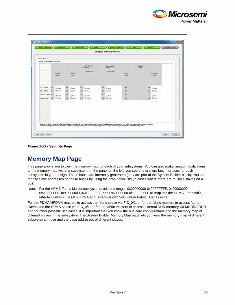
Security PageThis page enables you to configure your read and/or write access restrictions to the eSRAMs, eNVMs, FIC_0/1 and DDR_Bridge. This Security page is available only for devices that support advanced security denoted by the suffix "S" in the die name.
For details about how to configure security for your IGLOO2 device, refer to the HPMS Security Configuration User’s Guide.
Figure 2-22 • SECDED Page
Revision 7 29
Memory Map PageThis page allows you to view the memory map for each of your subsystems. You can also make limited modifications to the memory map within a subsystem. In the panel on the left, you see one or more bus interfaces for each subsystem in your design. These buses are internally generated (they are part of the System Builder block). You can modify slave addresses on these buses by using the drop down lists (in cases where there are multiple slaves on a bus).
Note: For the HPMS Fabric Master subsystems, address ranges 0x00000000-0x0FFFFFFF, 0x20000000-0x2FFFFFFF, 0x40000000-0x4FFFFFFF, and 0x60000000-0x6FFFFFFF all map into the HPMS. For details, refer to UG0445: IGLOO2 FPGA and SmartFusion2 SoC FPGA Fabric User's Guide.
For the PDMA/HPDMA masters to access the fabric space via FIC_0/1, or for the fabric masters to access fabric slaves and the HPMS space via FIC_0/1, or for the fabric masters to access external DDR memory via MDDR/FDDR and for other possible use cases, it is important that you know the bus core configurations and the memory map of different slaves in the subsystem. The System Builder Memory Map page lets you view the memory map of different subsystems in use and the base addresses of different slaves.
Figure 2-23 • Security Page
Revision 7 30
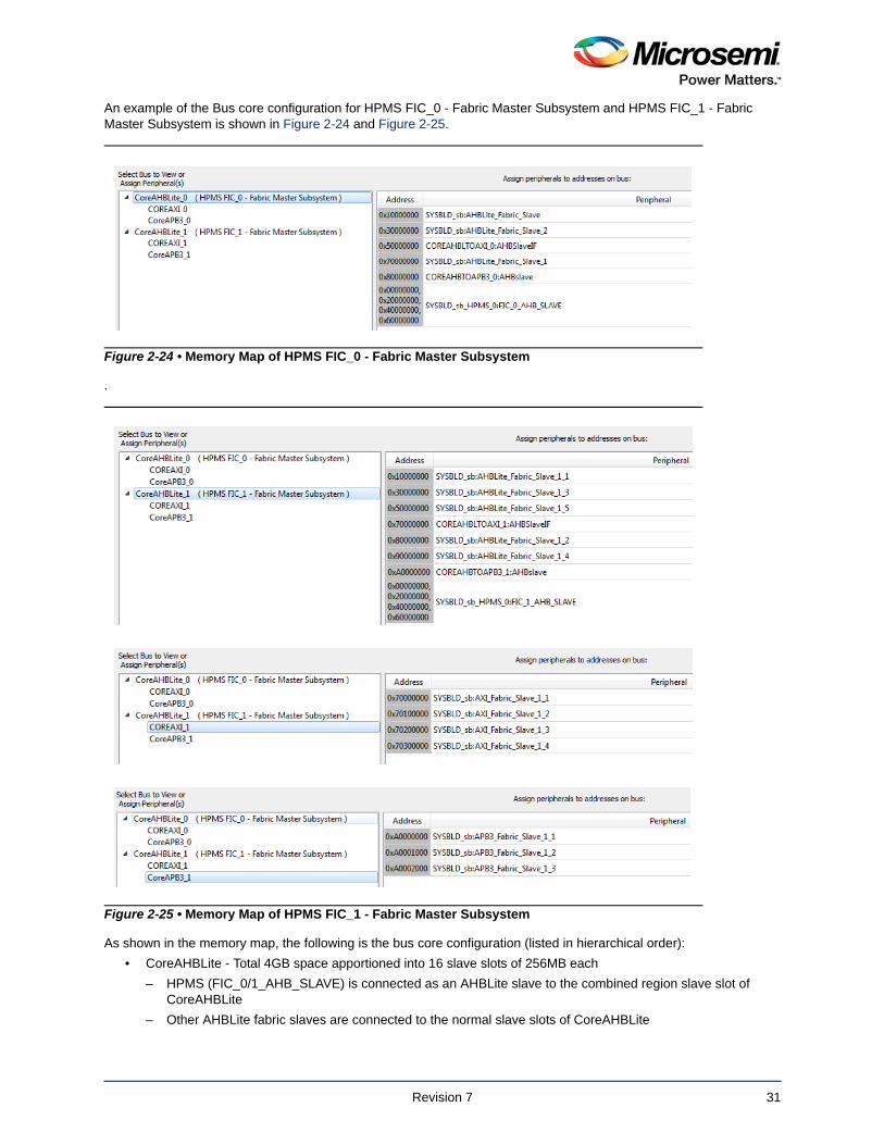
An example of the Bus core configuration for HPMS FIC_0 - Fabric Master Subsystem and HPMS FIC_1 - Fabric Master Subsystem is shown in Figure 2-24 and Figure 2-25.
.
As shown in the memory map, the following is the bus core configuration (listed in hierarchical order):
• CoreAHBLite - Total 4GB space apportioned into 16 slave slots of 256MB each
– HPMS (FIC_0/1_AHB_SLAVE) is connected as an AHBLite slave to the combined region slave slot of CoreAHBLite
– Other AHBLite fabric slaves are connected to the normal slave slots of CoreAHBLite
Figure 2-24 • Memory Map of HPMS FIC_0 - Fabric Master Subsystem
Figure 2-25 • Memory Map of HPMS FIC_1 - Fabric Master Subsystem
Revision 7 31
• CoreAXI - Total 16MB space apportioned into 16 slave slots of 1MB each
– AXI fabric slaves are connected to the slave slots of CoreAXI
• CoreAPB3 - Total 64KB space apportioned into 16 slave slots of 4KB each
– APB3 fabric slaves are connected to the slave slots of CoreAPB3
Revision 7 32
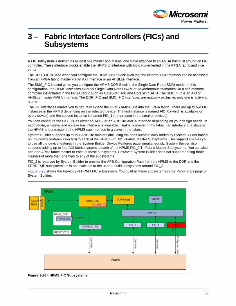
3 – Fabric Interface Controllers (FICs) and Subsystems
A FIC subsystem is defined as at least one master and at least one slave attached to an AMBA bus built around an FIC controller. These interface blocks enable the HPMS to interface with logic implemented in the FPGA fabric and vice versa.
The DDR_FIC is used when you configure the HPMS DDR block such that the external DDR memory can be accessed from an FPGA fabric master via an AXI interface or an AHBLite interface.
The SMC_FIC is used when you configure the HPMS DDR Block in the Single Date Rate (SDR) mode. In this configuration, the HPMS accesses external Single Data Rate DRAM or Asynchronous memories via a soft memory controller instantiated in the FPGA fabric such as CoreSDR_AXI and CoreSDR_AHB. The SMC_FIC is an AXI or AHBLite master AMBA interface. The DDR_FIC and SMC_FIC interfaces are mutually exclusive; only one is active at a time.
The FIC interfaces enable you to naturally extend the HPMS AMBA Bus into the FPGA fabric. There are up to two FIC instances in the HPMS depending on the selected device. The first instance is named FIC_0 (which is available on every device) and the second instance is named FIC_1 (not present in the smaller devices).
You can configure the FIC_0/1 as either an APB3 or an AHBLite AMBA interface depending on your design needs. In each mode, a master and a slave bus interface is available. That is, a master in the fabric can interface to a slave in the HPMS and a master in the HPMS can interface to a slave in the fabric.
System Builder supports up to four AHBLite masters (including the ones automatically added by System Builder based on the device features selected) to each of the HPMS FIC_0/1 - Fabric Master Subsystems. This support enables you to use all the device features in the System Builder Device Features page simultaneously. System Builder also supports adding up to four AXI fabric masters to each of the HPMS FIC_0/1 - Fabric Master Subsystems. You can also add one APB3 fabric master to each of these subsystems. However, System Builder does not support adding fabric masters of more than one type to any of the subsystems
FIC_2 is reserved by System Builder to provide the APB Configuration Path from the HPMS to the DDR and the SERDESIF subsystems. It is not available to the user to build subsystems around FIC_2.
Figure 3-26 shows the topology of HPMS FIC subsystems. You build all these subsystems in the Peripherals page of System Builder.
Figure 3-26 • HPMS FIC Subsystems
Revision 7 33
IGLOO2 HPMS FIC Subsystems
HPMS FIC_0 - Fabric Master SubsystemYou build this subsystem when you need to access the following IGLOO2 Device Features:
• HPMS eNVM/eSRAM/PDMA/SPI: Instantiate AHBLite User Fabric Master, or
• HPMS System Services: Instantiate the CoreSysServices IP
• HPMS HPDMA: Instantiate the CoreHPDMACtrl IP
• MDDR/FDDR/SERDESIF: No action required. System Builder automatically instantiates ConfigMaster IP inside the System Builder block.
This subsystem is available by default. It enables an AMBA AHBLite Fabric Master to access the HPMS memory space through FIC_0. Depending on your configuration, there can be up to four possible AHBLite Fabric Masters for this subsystem.
• ConfigMaster - This is a fabric core that drives the peripheral initialization process (i.e., the process of copying register configuration data from the eNVM to the DDR/SERDESIF). ConfigMaster is completely managed by System Builder, and you cannot modify it. For details, refer to the CoreConfigMaster IP Core User Guide (Catalog > Processors > CoreConfigMaster > Open Documentation).
• HPMS_FIC_0_USER_MASTER- If you select one of the eNVM, eSRAM, PDMA, or SPI (in the preceding Device Features page), this slot is meant for an AMBA AHBLite/APB3/AXI Fabric Master IP that is provided by you. You can access one of the above four components from your Fabric Master IP. Using this slot, you can read/write to the eNVM and eSRAM, and you can configure the PDMA/HPDMA registers to initiate DMA transfers. Your Fabric Master IP must generate AHBLite-compliant data transactions to be able to use this slot.
• HPMS_FIC_0_SYS_SERVICES_MASTER - If you select HPMS System Services in the Device Features page, this slot is meant for you to connect the CoreSysServices IP. After generating your system, you must configure and instantiate the soft IP core CoreSysServices from the IP Catalog into your top level SmartDesign. You must then connect the AHBLite Bus Interface (BIF) of the CoreSysServices to the HPMS_FIC_0_SYS_SERVICES_MASTER_BIF port exposed on the System Builder interface.
• HPMS_FIC_0_HPDMA_CONTROLLER_MASTER - If you select HPDMA in the Device Features page, this slot is meant for you to connect the CoreHPDMACtrl IP. After generating your system, you must configure and instantiate the soft IP core CoreHPDMACtrl from the IP Catalog into your top level SmartDesign. You must then connect the AHBLite Bus Interface (BIF) of the CoreHPDMACtrl to the HPMS_FIC_0_HPDMA_CONTROLLER_MASTER_BIF port exposed on the System Builder interface.
Connect your User Fabric Master or CoreSysServices IP or CoreHPDMACtrl IP to the System Builder block as shown in Table 3-1. System Builder automatically instantiates the ConfigMaster IP for you if you are using any of MDDR/FDDR/SERDES. You do not need to instantiate it. This subsystem supports up to four AHBLite-compliant masters. If you are using none of MDDR/FDDR/SERDESIF/HPMS System Services/HPMS HPDMA, you can add up to 4 AXI masters (including the configurable HPMS_FIC_0_USER_MASTER) to access the HPMS space including eSRAM/eNVM. Also, you can add 1 APB3 Fabric Master or configure the HPMS_FIC_0_USER_MASTER to be APB3 to access the HPMS space.
In addition to accessing the HPMS space, you can also have your fabric master access other fabric AMBA slaves added to the same subsystem. For each Fabric Slave you want to use in your design, drag and drop a Fabric AMBA Slave core from the available cores panel to this subsystem. Once a Fabric AMBA Slave core is in this subsystem, you can configure the core to set its AMBA protocol (to one of AHBLite/APB3/AXI). When you generate your system, you get an AMBA BIF (corresponding to the protocol you selected). In the top level SmartDesign, instantiate your actual Fabric Slave, and connect it to the appropriate slot in the generated system. You may add a mix of user slave types (Fabric AMBA Slaves - AXI/AHBLite/APB3) to this subsystem.
Revision 7 34
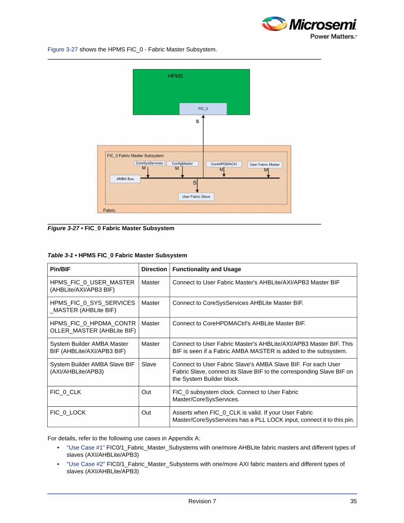
Figure 3-27 shows the HPMS FIC_0 - Fabric Master Subsystem.
For details, refer to the following use cases in Appendix A:
• "Use Case #1" FIC0/1_Fabric_Master_Subystems with one/more AHBLite fabric masters and different types of slaves (AXI/AHBLite/APB3)
• "Use Case #2" FIC0/1_Fabric_Master_Subystems with one/more AXI fabric masters and different types of slaves (AXI/AHBLite/APB3)
Figure 3-27 • FIC_0 Fabric Master Subsystem
Table 3-1 • HPMS FIC_0 Fabric Master Subsystem
Pin/BIF Direction Functionality and Usage
HPMS_FIC_0_USER_MASTER (AHBLite/AXI/APB3 BIF)
Master Connect to User Fabric Master's AHBLite/AXI/APB3 Master BIF
HPMS_FIC_0_SYS_SERVICES_MASTER (AHBLite BIF)
Master Connect to CoreSysServices AHBLite Master BIF.
HPMS_FIC_0_HPDMA_CONTROLLER_MASTER (AHBLite BIF)
Master Connect to CoreHPDMACtrl's AHBLite Master BIF.
System Builder AMBA Master BIF (AHBLite/AXI/APB3 BIF)
Master Connect to User Fabric Master's AHBLite/AXI/APB3 Master BIF. This BIF is seen if a Fabric AMBA MASTER is added to the subsystem.
System Builder AMBA Slave BIF (AXI/AHBLite/APB3)
Slave Connect to User Fabric Slave's AMBA Slave BIF. For each User Fabric Slave, connect its Slave BIF to the corresponding Slave BIF on the System Builder block.
FIC_0_CLK Out FIC_0 subsystem clock. Connect to User Fabric Master/CoreSysServices.
FIC_0_LOCK Out Asserts when FIC_0_CLK is valid. If your User Fabric Master/CoreSysServices has a PLL LOCK input, connect it to this pin.
Revision 7 35
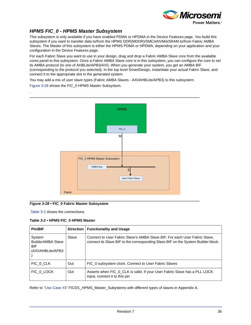
HPMS FIC_0 - HPMS Master SubsystemThis subsystem is only available if you have enabled PDMA or HPDMA in the Device Features page. You build this subsystem if you want to transfer data to/from the HPMS DDR(MDDR)/SMC/eNVM/eSRAM to/from Fabric AMBA Slaves. The Master of this subsystem is either the HPMS PDMA or HPDMA, depending on your application and your configuration in the Device Features page.
For each Fabric Slave you want to use in your design, drag and drop a Fabric AMBA Slave core from the available cores panel to this subsystem. Once a Fabric AMBA Slave core is in this subsystem, you can configure the core to set its AMBA protocol (to one of AHBLite/APB3/AXI). When you generate your system, you get an AMBA BIF (corresponding to the protocol you selected). In the top level SmartDesign, instantiate your actual Fabric Slave, and connect it to the appropriate slot in the generated system.
You may add a mix of user slave types (Fabric AMBA Slaves - AXI/AHBLite/APB3) to this subsystem.
Figure 3-28 shows the FIC_0 HPMS Master Subsystem.
.
.Table 3-2 shows the connections.
Refer to "Use Case #3" FIC0/1_HPMS_Master_Subystems with different types of slaves in Appendix A.
Figure 3-28 • FIC_0 Fabric Master Subsystem
Table 3-2 • HPMS FIC_0 HPMS Master
Pin/BIF Direction Functionality and Usage
System BuilderAMBA Slave BIF (AXI/AHBLite/APB3)
Slave Connect to User Fabric Slave's AMBA Slave BIF. For each User Fabric Slave, connect its Slave BIF to the corresponding Slave BIF on the System Builder block.
FIC_0_CLK Out FIC_0 subsystem clock. Connect to User Fabric Slaves
FIC_0_LOCK Out Asserts when FIC_0_CLK is valid. If your User Fabric Slave has a PLL LOCK input, connect it to this pin
Revision 7 36
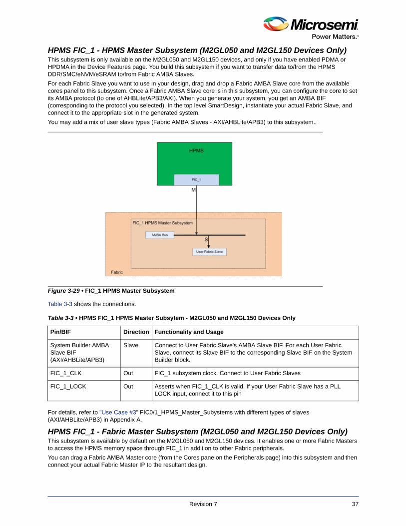
HPMS FIC_1 - HPMS Master Subsystem (M2GL050 and M2GL150 Devices Only)This subsystem is only available on the M2GL050 and M2GL150 devices, and only if you have enabled PDMA or HPDMA in the Device Features page. You build this subsystem if you want to transfer data to/from the HPMS DDR/SMC/eNVM/eSRAM to/from Fabric AMBA Slaves.
For each Fabric Slave you want to use in your design, drag and drop a Fabric AMBA Slave core from the available cores panel to this subsystem. Once a Fabric AMBA Slave core is in this subsystem, you can configure the core to set its AMBA protocol (to one of AHBLite/APB3/AXI). When you generate your system, you get an AMBA BIF (corresponding to the protocol you selected). In the top level SmartDesign, instantiate your actual Fabric Slave, and connect it to the appropriate slot in the generated system.
You may add a mix of user slave types (Fabric AMBA Slaves - AXI/AHBLite/APB3) to this subsystem..
Table 3-3 shows the connections.
For details, refer to "Use Case #3" FIC0/1_HPMS_Master_Subystems with different types of slaves (AXI/AHBLite/APB3) in Appendix A.
HPMS FIC_1 - Fabric Master Subsystem (M2GL050 and M2GL150 Devices Only) This subsystem is available by default on the M2GL050 and M2GL150 devices. It enables one or more Fabric Masters to access the HPMS memory space through FIC_1 in addition to other Fabric peripherals.
You can drag a Fabric AMBA Master core (from the Cores pane on the Peripherals page) into this subsystem and then connect your actual Fabric Master IP to the resultant design.
Figure 3-29 • FIC_1 HPMS Master Subsystem
Table 3-3 • HPMS FIC_1 HPMS Master Subsytem - M2GL050 and M2GL150 Devices Only
Pin/BIF Direction Functionality and Usage
System Builder AMBA Slave BIF (AXI/AHBLite/APB3)
Slave Connect to User Fabric Slave's AMBA Slave BIF. For each User Fabric Slave, connect its Slave BIF to the corresponding Slave BIF on the System Builder block.
FIC_1_CLK Out FIC_1 subsystem clock. Connect to User Fabric Slaves
FIC_1_LOCK Out Asserts when FIC_1_CLK is valid. If your User Fabric Slave has a PLL LOCK input, connect it to this pin
Revision 7 37
The subsystem supports up to four AHBLite/AXI fabric masters, and one APB3 fabric master. You may not mix and use more than one master type. You may, however, use a mix of different fabric slaves types (AHBLite/AXI/APB3) in this subsystem
You can configure your Fabric AMBA Master core to one of AHBLite/APB3/AXI to correspond to your Fabric Master IP. Using your Fabric Master, you can access the eNVM and eSRAM, and the PDMA or HPDMA configuration registers inside the HPMS.
You can use the FIC_1 Fabric Master Subsystem to access HPMS features such as:
• HPMS System Services - Add an AHBLite Fabric AMBA Master Core in System Builder and connect the resultant AHBLite master bus interface port on the System Builder generated design to the CoreSysServices IP (available in the IP Catalog)
• eSRAM/eNVM/PDMA/HPDMA/SPI - Using your own AMBA-compliant Fabric Master
In addition to accessing the HPMS space, you can also have your fabric master access other fabric AMBA slaves added to the same subsystem. For each Fabric Slave you want to use in your design, drag and drop a Fabric AMBA Slave core from the available cores panel to this subsystem. Once a Fabric AMBA Slave core is in this subsystem, you can configure the core to set its AMBA protocol (to one of AHBLite/APB3/AXI). When you generate your system, you get an AMBA BIF (corresponding to the protocol you selected). In the top level SmartDesign, instantiate your actual Fabric Slave, and connect it to the appropriate slot in the generated system.
Note: If you instantiate an APB3 Fabric Master in your FIC_1 Fabric Master Subsystem, System Builder configures the FIC_1 interface and the corresponding CoreAPB3 to be compatible with CoreABC-like APB3 Fabric Masters. In other words, System Builder automatically configures the APB3 Fabric Master interface with the following characteristics:
• 32-bit data bus
• 20 bits of address
– Lower 16 bits passed directly to the HPMS
– Upper 4 bits select 1 of 16 APB slave slots
Slot 0 - HPMS
Slots 1-14 - Fabric Slaves
Slot 15 - Indirect Addressing register
To access different HPMS address spaces, your APB3 Fabric Master must first write the base address (32-bits, lower 16 bits set to zero) into the Indirect Addressing register. For any subsequent transactions on this interface, the address "seen" by the HPMS will consist of the upper 16 bits stored in the Indirect Addressing register and the lower 16 bits driven by the User Fabric Master.
Revision 7 38
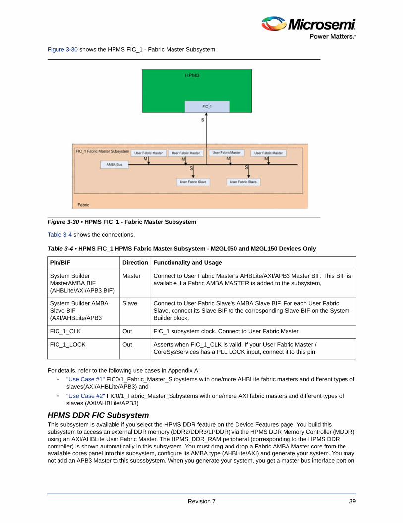
Figure 3-30 shows the HPMS FIC_1 - Fabric Master Subsystem.
Table 3-4 shows the connections.
For details, refer to the following use cases in Appendix A:
• "Use Case #1" FIC0/1_Fabric_Master_Subystems with one/more AHBLite fabric masters and different types of slaves(AXI/AHBLite/APB3) and
• "Use Case #2" FIC0/1_Fabric_Master_Subystems with one/more AXI fabric masters and different types of slaves (AXI/AHBLite/APB3)
HPMS DDR FIC SubsystemThis subsystem is available if you select the HPMS DDR feature on the Device Features page. You build this subsystem to access an external DDR memory (DDR2/DDR3/LPDDR) via the HPMS DDR Memory Controller (MDDR) using an AXI/AHBLite User Fabric Master. The HPMS_DDR_RAM peripheral (corresponding to the HPMS DDR controller) is shown automatically in this subsystem. You must drag and drop a Fabric AMBA Master core from the available cores panel into this subsystem, configure its AMBA type (AHBLite/AXI) and generate your system. You may not add an APB3 Master to this subssbystem. When you generate your system, you get a master bus interface port on
Figure 3-30 • HPMS FIC_1 - Fabric Master Subsystem
Table 3-4 • HPMS FIC_1 HPMS Fabric Master Subsystem - M2GL050 and M2GL150 Devices Only
Pin/BIF Direction Functionality and Usage
System Builder MasterAMBA BIF (AHBLite/AXI/APB3 BIF)
Master Connect to User Fabric Master’s AHBLite/AXI/APB3 Master BIF. This BIF is available if a Fabric AMBA MASTER is added to the subsystem,
System Builder AMBA Slave BIF (AXI/AHBLite/APB3
Slave Connect to User Fabric Slave's AMBA Slave BIF. For each User Fabric Slave, connect its Slave BIF to the corresponding Slave BIF on the System Builder block.
FIC_1_CLK Out FIC_1 subsystem clock. Connect to User Fabric Master
FIC_1_LOCK Out Asserts when FIC_1_CLK is valid. If your User Fabric Master / CoreSysServices has a PLL LOCK input, connect it to this pin
Revision 7 39
the System Builder generated design which you must connect to your actual Fabric Master IP in the top level SmartDesign.
Optionally, you may add Fabric Slaves to this subsystem. You may add a mix of user slave types (Fabric AMBA Slaves - AXI/AHBLite/APB3) to this subsystem. The User Fabric Master accessing the external DDR memory via the HPMS DDR (MDDR) will be the master to these Fabric Slaves as well.
Alternatively, you may allow the HPDMA controller to access an external DDR memory (DDR2/DDR3/LPDDR) via HPMS DDR (MDDR); and manage data transfers to and from eSRAM/eNVM/Fabric Slaves. The HPDMA controller enables you to initiate transfers between the external DDR memory via HPMS DDR (MDDR) at one end and eSRAM/eNVM (read only)/Fabric Slaves at the other end.
Figure 3-31 shows the HPMS DDR FIC Subsystem.
Table 3-5 shows the connections.
Figure 3-31 • HPMS DDR FIC Subsystem
Table 3-5 • HPMS DDR FIC Subsystem
Pin/BIF Direction Functionality and Usage
System Builder Master (AHBLite /AXI) BIF Master (MDDR)
Connect to User Fabric Master's AMBA Master BIF.
System Builder Slave (AHBLite/AXI/APB3) BIF
Slave Connect to User Fabric Slave's AMBA Slave BIF.
HPMS_DDR_FIC_SUBSYSTEM_PINS:
HPMS_DDR_FIC_SUBSYSTEM_CLK
Out HPMS DDR subsystem clock. Connect to User Fabric Master and User Fabric Slaves in this subsystem.
HPMS_DDR_FIC_SUBSYSTEM_PINS:
HPMS_DDR_FIC_SUBSYSTEM_LOCK
Out Asserts when HPMS_DDR_FIC_SUBSYSTEM_CLK is valid. If your User Fabric Master/User Fabric Slaves have PLL LOCK inputs, connect them to this pin.
Revision 7 40
For details, refer to the following use cases in Appendix A:
• "Use Case #4" HPMS DDR_FIC_Subsystem with one AHBLite fabric master and different types of slaves(AXI/AHBLite/APB3)
• "Use Case #5" HPMS DDR_FIC_Subsystem with one AXI fabric master and different types of slaves (AXI/AHBLite/APB3)
• "Use Case #6" HPMS DDR_FIC_Subsystem with one AXI fabric master and no other slaves
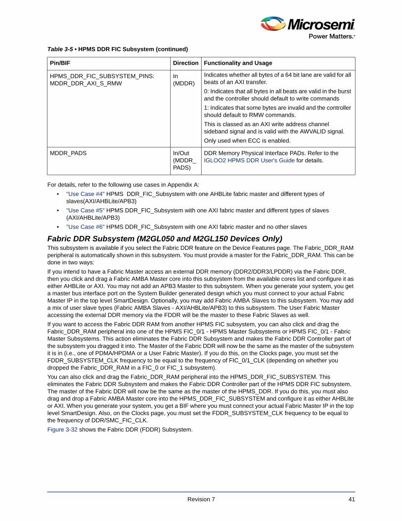
Fabric DDR Subsystem (M2GL050 and M2GL150 Devices Only)This subsystem is available if you select the Fabric DDR feature on the Device Features page. The Fabric_DDR_RAM peripheral is automatically shown in this subsystem. You must provide a master for the Fabric_DDR_RAM. This can be done in two ways:
If you intend to have a Fabric Master access an external DDR memory (DDR2/DDR3/LPDDR) via the Fabric DDR, then you click and drag a Fabric AMBA Master core into this subsystem from the available cores list and configure it as either AHBLite or AXI. You may not add an APB3 Master to this subsystem. When you generate your system, you get a master bus interface port on the System Builder generated design which you must connect to your actual Fabric Master IP in the top level SmartDesign. Optionally, you may add Fabric AMBA Slaves to this subsystem. You may add a mix of user slave types (Fabric AMBA Slaves - AXI/AHBLite/APB3) to this subsystem. The User Fabric Master accessing the external DDR memory via the FDDR will be the master to these Fabric Slaves as well.
If you want to access the Fabric DDR RAM from another HPMS FIC subsystem, you can also click and drag the Fabric_DDR_RAM peripheral into one of the HPMS FIC_0/1 - HPMS Master Subsystems or HPMS FIC_0/1 - Fabric Master Subsystems. This action eliminates the Fabric DDR Subsystem and makes the Fabric DDR Controller part of the subsystem you dragged it into. The Master of the Fabric DDR will now be the same as the master of the subsystem it is in (i.e., one of PDMA/HPDMA or a User Fabric Master). If you do this, on the Clocks page, you must set the FDDR_SUBSYSTEM_CLK frequency to be equal to the frequency of FIC_0/1_CLK (depending on whether you dropped the Fabric_DDR_RAM in a FIC_0 or FIC_1 subsystem).
You can also click and drag the Fabric_DDR_RAM peripheral into the HPMS_DDR_FIC_SUBSYSTEM. This eliminates the Fabric DDR Subsystem and makes the Fabric DDR Controller part of the HPMS DDR FIC subsystem. The master of the Fabric DDR will now be the same as the master of the HPMS_DDR. If you do this, you must also drag and drop a Fabric AMBA Master core into the HPMS_DDR_FIC_SUBSYSTEM and configure it as either AHBLite or AXI. When you generate your system, you get a BIF where you must connect your actual Fabric Master IP in the top level SmartDesign. Also, on the Clocks page, you must set the FDDR_SUBSYSTEM_CLK frequency to be equal to the frequency of DDR/SMC_FIC_CLK.
Figure 3-32 shows the Fabric DDR (FDDR) Subsystem.
HPMS_DDR_FIC_SUBSYSTEM_PINS: MDDR_DDR_AXI_S_RMW
In (MDDR)
Indicates whether all bytes of a 64 bit lane are valid for all beats of an AXI transfer.
0: Indicates that all bytes in all beats are valid in the burst and the controller should default to write commands
1: Indicates that some bytes are invalid and the controller should default to RMW commands.
This is classed as an AXI write address channel sideband signal and is valid with the AWVALID signal.
Only used when ECC is enabled.
MDDR_PADS In/Out (MDDR_PADS)
DDR Memory Physical Interface PADs. Refer to the IGLOO2 HPMS DDR User's Guide for details.
Table 3-5 • HPMS DDR FIC Subsystem (continued)
Pin/BIF Direction Functionality and Usage
Revision 7 41
Connect your User Fabric Master and User Fabric Slaves to the System Builder block as shown in Table 3-6.
Figure 3-32 • Fabric DDR (FDDR) Subsystem
Table 3-6 • Fabric DDR Subsystem - M2GL050 and M2GL150 Devices Only
Pin/BIF Direction Functionality and Usage
System Builder Master (AHBLite /AXI) BIF Master Connect to User Fabric Master's AMBA Master BIF.
System Builder Slave (AHBLite/AXI/APB3) BIF
Slave Connect to User Fabric Slave's AMBA Slave BIF.
Revision 7 42
For details, refer to the following use cases in Appendix A:
• "Use Case #7" Fabric_DDR_Subsystem with one AHBLite fabric master and different types of slaves (AXI/AHBLite/APB3)
• "Use Case #8" Fabric_DDR_Subsystem with one AXI fabric master and different types of slaves (AXI/AHBLite/APB3)
• "Use Case #9" Fabric_DDR_Subsystem with one AXI fabric master and no other slaves
FDDR_SUBSYSTEM_PINS:FDDR_SUBSYSTEM_CLK
In Fabric DDR subsystem clock. You must provide a clock for your Fabric DDR Subsystem using one of the following options:
• Instantiate Fabric CCC in SmartDesign to generate the clock for the FDDR subsystem. The Fabric CCC will generate a clock and PLL lock signals. Connect Fabric CCC's Clock output (GL0/1/2/3) to:
• FDDR_SUBSYSTEM_CLK
• User Fabric Master's Clock Input
• User Fabric Slaves' Clock Inputs
• If you want to use the same clock frequency as one of the other subsystems (FIC_0/1 or HPMS DDR), instead of instantiating a Fabric CCC, you can get the appropriate clock and lock signals from your chosen subsystem's pins. Connect your chosen clock signal (one of FIC_0_CLK, FIC_1_CLK, or HPMS_DDR_FIC_SUBSYSTEM_CLK) to:
• FDDR_SUBSYSTEM_CLK
• User Fabric Master's Clock Input
• User Fabric Slaves' Clock Inputs
FDDR_SUBSYSTEM_PINS:FDDR_SUBSYSTEM_CLK_PLL_LOCK
In Asserts when FDDR_SUBSYSTEM_CLK is valid. Depending on your selection of the driver of FDDR_SUBSYSTEM_CLK, connect to one of the following:
• Fabric CCC:LOCK
• System Builder block's FIC_0_LOCK, FIC_1_LOCK, or HPMS_DDR_FIC_SUBSYSTEM_LOCK
FDDR_SUBSYSTEM_PINS:
FDDR_SUBSYSTEM_RESET_ N
In Reset the FDDR subsystems. You may connect the HPMS_READY signal or DDR_READY signal or other user fabric logic signal to this pin at the top level.
FDDR_SUBSYSTEM_PINS:FDDR_AXI_S_RMW
In Indicates whether all bytes of a 64 bit lane are valid for all beats of an AXI transfer.
0: Indicates that all bytes in all beats are valid in the burst and the controller should default to write commands
1: Indicates that some bytes are invalid and the controller should default to RMW commands
This is classed as an AXI write address channel sideband signal and is valid with the AWVALID signal.
Only used when ECC is enabled
FDDR_PADS In/Out DDR Memory Physical Interface PADs. Refer to the IGLOO2 HPMS DDR User's Guide for details.
Table 3-6 • Fabric DDR Subsystem - M2GL050 and M2GL150 Devices Only (continued)
Pin/BIF Direction Functionality and Usage
Revision 7 43
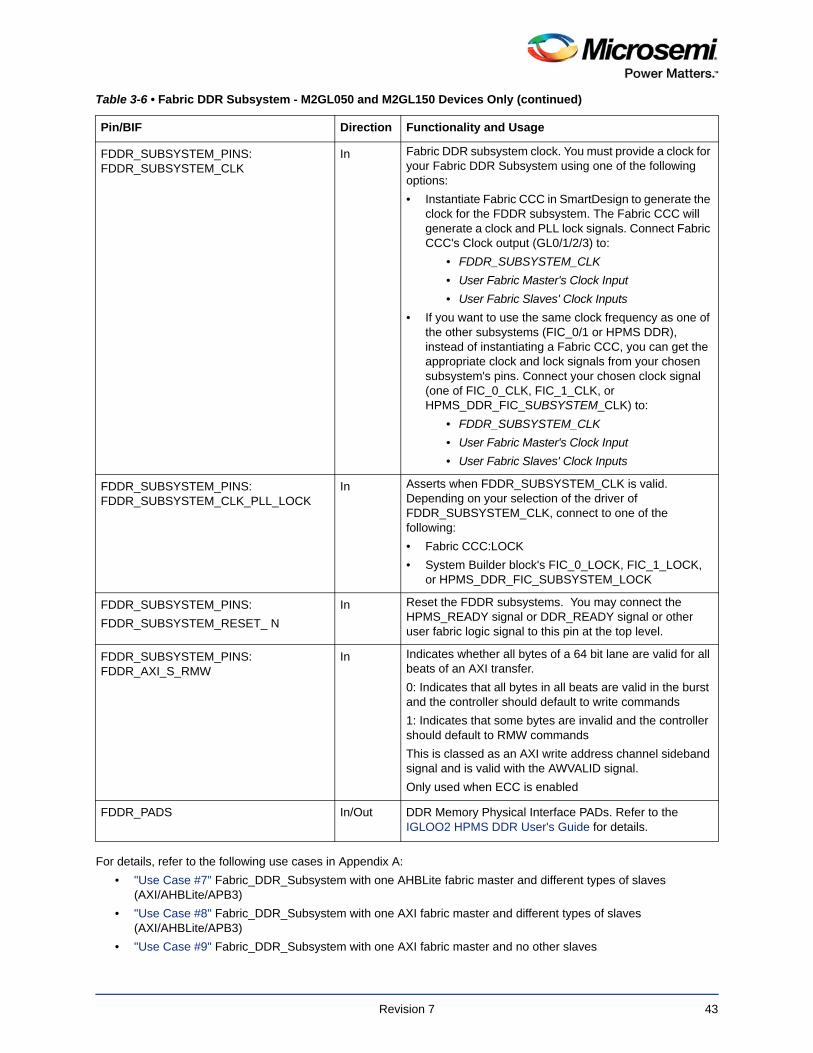
HPMS SMC FIC SubsystemThis subsystem is available in the Peripherals page if you select the SMC (Soft Memory Controller) in the Device Features page. HPMS High Performance DMA (HPDMA) is selected automatically in the Device Features page if you select SMC.
You build this subsystem to use the IGLOO2 Soft Memory Controller Fabric Interface Controller (SMC_FIC) to access external bulk memories other than DDR, such as SDRAM. The HPDMA controller accesses external Single Data Rate DRAM or Asynchronous memories via this SMC_FIC and a soft memory controller instantiated by System Builder in the FPGA fabric such as CoreSDR_AXI and CoreSDR_AHB and manages data transfers to and from eSRAM/eNVM/Fabric Slaves. The HPDMA controller enables you to initiate transfers between the external SDR RAM via SMC_FIC at one end and eSRAM/eNVM (read only)/Fabric Slaves at the other end.
Figure 3-33 shows the SMC_FIC Subsystem.
Click the Configure icon next to the HPMS_SMC instance in the Peripherals page to configure the specific external memory parameters (width, timing, etc.), as shown in Figure 3-34 below.
System Builder exposes the SMC interface ports(HPMS_SMC_0_PINS) to the top level.
If the SMC_FIC is enabled, the MDDR subsystem is not available. In SMC_FIC mode, the DDR I/O’s associated with the MDDR subsystem are released and are available as general FPGA Fabric I/O’s.
Note: To use the HPMS SMC, you must select SMC and HPMS High Performance DMA (HPDMA) in the Device Features page.
As the HPDMA is automatically used, a BIF port for a Fabric Master is exposed on the System Builder interface in the resultant design. You must connect your Fabric AMBA Master or the CoreHPDMACtrl soft IP core (from the IP Catalog) to this port to access the HPDMA configuration registers.
Figure 3-33 • SMC FIC Subsystem
Revision 7 44
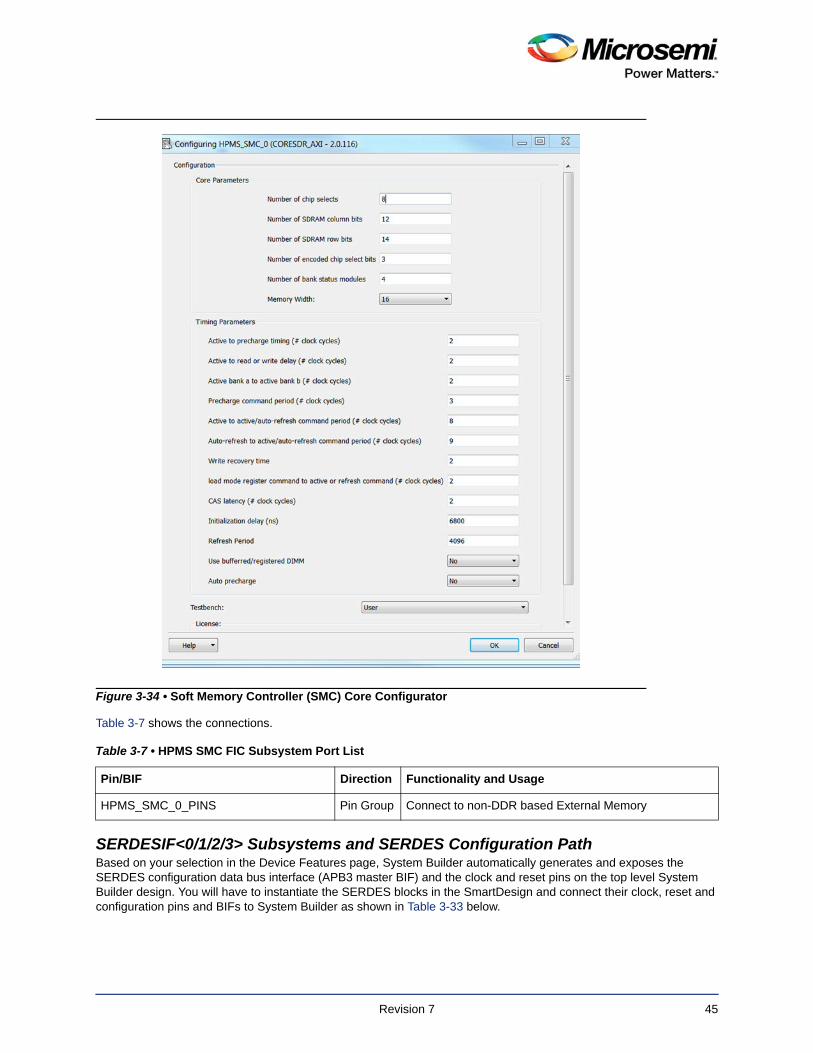
Table 3-7 shows the connections.
SERDESIF<0/1/2/3> Subsystems and SERDES Configuration Path Based on your selection in the Device Features page, System Builder automatically generates and exposes the SERDES configuration data bus interface (APB3 master BIF) and the clock and reset pins on the top level System Builder design. You will have to instantiate the SERDES blocks in the SmartDesign and connect their clock, reset and configuration pins and BIFs to System Builder as shown in Table 3-33 below.
Figure 3-34 • Soft Memory Controller (SMC) Core Configurator
Table 3-7 • HPMS SMC FIC Subsystem Port List
Pin/BIF Direction Functionality and Usage
HPMS_SMC_0_PINS Pin Group Connect to non-DDR based External Memory
Revision 7 45
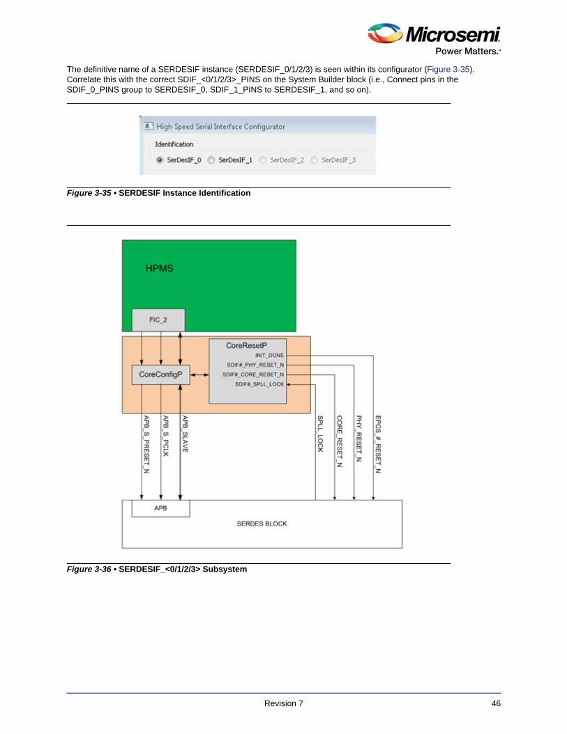
The definitive name of a SERDESIF instance (SERDESIF_0/1/2/3) is seen within its configurator (Figure 3-35). Correlate this with the correct SDIF_<0/1/2/3>_PINS on the System Builder block (i.e., Connect pins in the SDIF_0_PINS group to SERDESIF_0, SDIF_1_PINS to SERDESIF_1, and so on).
Figure 3-35 • SERDESIF Instance Identification
Figure 3-36 • SERDESIF_<0/1/2/3> Subsystem
Revision 7 46
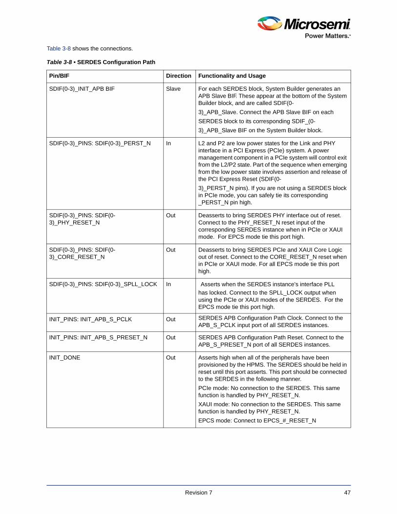
Table 3-8 shows the connections.
Table 3-8 • SERDES Configuration Path
Pin/BIF Direction Functionality and Usage
SDIF(0-3)_INIT_APB BIF Slave For each SERDES block, System Builder generates an APB Slave BIF. These appear at the bottom of the System Builder block, and are called SDIF(0-
3)_APB_Slave. Connect the APB Slave BIF on each
SERDES block to its corresponding SDIF_(0-
3)_APB_Slave BIF on the System Builder block.
SDIF(0-3)_PINS: SDIF(0-3)_PERST_N In L2 and P2 are low power states for the Link and PHY interface in a PCI Express (PCIe) system. A power management component in a PCIe system will control exit from the L2/P2 state. Part of the sequence when emerging from the low power state involves assertion and release of the PCI Express Reset (SDIF(0-
3)_PERST_N pins). If you are not using a SERDES block in PCIe mode, you can safely tie its corresponding _PERST_N pin high.
SDIF(0-3)_PINS: SDIF(0-3)_PHY_RESET_N
Out Deasserts to bring SERDES PHY interface out of reset. Connect to the PHY_RESET_N reset input of the corresponding SERDES instance when in PCIe or XAUI mode. For EPCS mode tie this port high.
SDIF(0-3)_PINS: SDIF(0-3)_CORE_RESET_N
Out Deasserts to bring SERDES PCIe and XAUI Core Logic out of reset. Connect to the CORE_RESET_N reset when in PCIe or XAUI mode. For all EPCS mode tie this port high.
SDIF(0-3)_PINS: SDIF(0-3)_SPLL_LOCK In Asserts when the SERDES instance's interface PLL
has locked. Connect to the SPLL_LOCK output when using the PCIe or XAUI modes of the SERDES. For the EPCS mode tie this port high.
INIT_PINS: INIT_APB_S_PCLK Out SERDES APB Configuration Path Clock. Connect to the APB_S_PCLK input port of all SERDES instances.
INIT_PINS: INIT_APB_S_PRESET_N Out SERDES APB Configuration Path Reset. Connect to the APB_S_PRESET_N port of all SERDES instances.
INIT_DONE Out Asserts high when all of the peripherals have been provisioned by the HPMS. The SERDES should be held in reset until this port asserts. This port should be connected to the SERDES in the following manner.
PCIe mode: No connection to the SERDES. This same function is handled by PHY_RESET_N.
XAUI mode: No connection to the SERDES. This same function is handled by PHY_RESET_N.
EPCS mode: Connect to EPCS_#_RESET_N
Revision 7 47
System Builder Reset and Miscellaneous PinsThe System Builder block receives and generates reset signals shown in Table 3-9; they can be connected to your user logic or board. The actual pins available depends on your design.
Table 3-9 • Reset Pins
Pin Direction Functionality and Usage
DEVRST_N (PAD) In FPGA Power ON Reset. Automatically promoted to top level. Deasserts when FPGA is powered up for the first time. This active-low reset will perform the same function as a power-up reset; it is an optional function and can be safely be tied high in your test bench.
FAB_RESET_N In Fabric to System Builder block reset. Can be used by your Fabric logic to reset the system (HPMS/SERDES/DDR). This active-low reset will perform a re-initialization of all of the peripherals controlled by the HPMS. This is an optional function and can safely be tied high.
INIT_PINS:INIT_DONE Out Value 1 indicates that System Builder block components are ready for communication and initialization is complete. Connect to any fabric logic that needs to wait for System Builder initialization.
POWER_ON_RESET_N Out Value 0 indicates the system controller is in the process of booting. Goes to 0 just after the VDD ramps past the threshold voltage.
Value 1 indicates the system controller is finished booting.
HPMS_READY Out Value 1 indicates the HPMS is ready for communication with the fabric logic. Connect to User logic/CoreSysServices's Reset input.
HPMS_READY will assert before the INIT_DONE pins go high. This output only indicates the HPMS FICs can be accessed, not that the entire system is operational. To wait until the entire system is operational, wait for HPMS_READY and all of the applicable INIT_DONE pins to go high.
DDR_READY Out This pin is seen only when one/both of MDDR/FDDR are used in the design. Value "1" indicates that both MDDR and FDDR (if used) blocks are ready for communication and their initialization is complete. Connect to any fabric logic that needs to wait for MDDR/FDDR initialization.
SDIF_READY Out This pin is seen only when one/more SERDES blocks are used in the design. Value "1" indicates that all the SERDES blocks (if used) are ready for communication and their initialization is complete. Connect to any fabric logic that needs to wait for SERDES initialization.
Table 3-10 • Miscellaneous Pins
Pin Direction Functionality and Usage
<instance>_HPMS_0_PINS: COMM_BLK_INT
Out For details, refer to the Microsemi IGLOO2 User's Guide
<instance>_HPMS_0_PINS: HPMS_M2F_INT[15:0]
Out HPMS Peripheral Interrupt. For details, refer to the Microsemi
IGLOO2 User's Guide
<instance>_HPMS_0_PINS: DMA_DMAREADY_FIC_0[1:0]
In For details, refer to the Microsemi IGLOO2 User's Guide
Revision 7 48
<instance>_HPMS_0_PINS: DMA_DMAREADY_FIC_1[1:0]
In For details, refer to the Microsemi IGLOO2 User's Guide
FAB_CCC_PINS: FAB_CCC_GL(0/1/2/3)
Out Connect to the clock pins of user fabric logic.
FAB_CCC_PINS:
FAB_CCC_LOCK
Out Exposed when FAB_CCC_GL(0/1/2/3) is exposed. When high, FAB_CCC_LOCK signal indicates that the clocks FAB_CCC_GL(0-3) are valid.
CLK(0/1/2/3)_PAD In Dedicated Input pad Reference Clock to the Fabric CCC.
CCC_0_PINS:
CLK(0/1/2/3)
In FPGA Fabric Input Reference Clock to the Fabric CCC.
XTL In Input source to the External Main Crystal Oscillator.
CHIP_OSC_PINS:
XTLOSC_O2F
Out Crystal Oscillator output. Used to drive user fabric logic or the Fabric CCC.
CHIP_OSC_PINS: RCOSC_1MHZ_O2F
Out 1 MHz RC Oscillator output. Used to drive user fabric logic or the Fabric CCC.
CHIP_OSC_PINS: RCOSC_25_50MHZ_O2F
Out 25/50 MHz RC Oscillator output. Used to drive the input RCOSC_25_50MHZ_CCC_IN BIF pin of Fabric CCC.
XTLOSC_CCC_OUT Out/BIF Crystal Oscillator output. Used to drive the input XTLOSC_CCC_IN BIF pin of Fabric CCC.
RCOSC_1MHZ_CCC_OUT Out/BIF 1 MHz RC Oscillator output. Used to drive the input RCOSC_1MHZ_CCC_IN BIF pin of Fabric CCC.
RCOSC_25_50MHZ_CCC_OUT Out/BIF 25/50 MHz RC Oscillator output. Used to drive the input RCOSC_25_50MHZ_CCC_IN BIF pin of Fabric CCC.
Table 3-10 • Miscellaneous Pins (continued)
Pin Direction Functionality and Usage
Revision 7 49
4 – Generated System
After generating your design you will end up with two new components in your Design Hierarchy. There will be a component named <design_name>, which is a SmartDesign that instantiates your System Builder generated component <design_name>_sb.
The <design_name> is a regular SmartDesign that contains an instance of your System Builder block. Double-click the <design_name>_sb component in your Design Hierarchy or double-click the System Builder instance in the <design_name> SmartDesign canvas to reconfigure the System Builder. When your design is reopened in System Builder, you will observe that all your configuration options that you specified while creating the design are preserved.
Figure 4-37 shows the Design Hierarchy after clicking Finish in the final System Builder page for a system named mytop.
The SmartDesign Canvas displays the instance of the System Builder generated component (Figure 4-38).Based on your selections in System Builder, the generated block will contain sets of pins and Bus Interfaces (usually a set of pins per subsystem, and one BIF per master or slave in that subsystem).
The <design_name> SmartDesign Canvas displays the instance of the System Builder generated component. You can choose to add your own custom peripherals or logic to the <design_name> SmartDesign at this point and connect them to the System Builder instance accordingly.
Your System Builder design is summarized in the System Builder summary report in the Libero Reports View. The name of this file is <design_name>_sb_SYS_BLD.xml. Open the Reports View and click this file for details on what was generated in your System Builder component.
Depending on the type of subsystems you have configured for the System Builder block, the System Builder block may have the ports exposed at the top level, as shown in Figure 4-38.
Figure 4-37 • Design Hierarchy After System Builder Generates the Block
Revision 7 50
.
Figure 4-38 • System Builder Component on the SmartDesign Canvas
Revision 7 51
5 – Modifying/Inspecting Your System Builder Design
When System Builder successfully generates your design, it does the following:
• Generates the Initialization circuitry for your peripherals.
• Generates the Reset circuitry for your peripherals
• Instantiates the Clock networks including the CCC per your system requirement.
• Instantiates and configures the AMBA bus for your subsystem per your system requirement.
Items #1 and #2 are excluded when you choose to run System Builder using the Standalone Initialization Methodology (Project > Project Settings > Design Flow > Use Standalone Initialization for MDDR/FDDR.SERDES peripherals). For details, refer to the IGLOO2 Standalone Peripheral Initialization User Guide.
Note: Item #4 is excluded when you choose the Direct Connection Mode (System Builder > Peripherals > Direct Connection Mode).
Revision 7 52
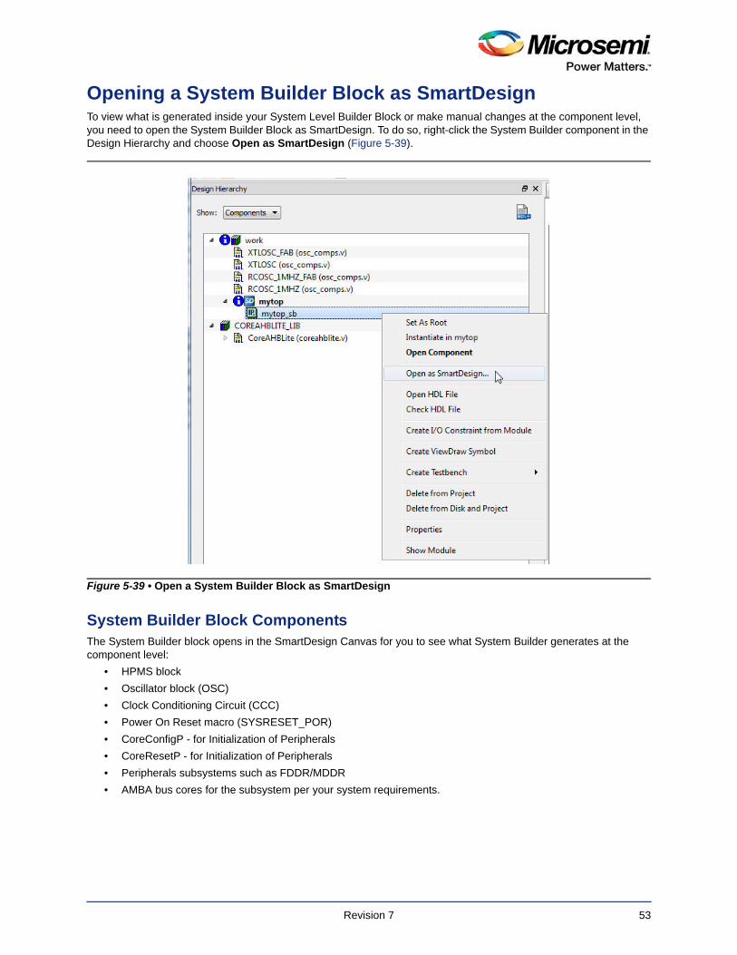
Opening a System Builder Block as SmartDesignTo view what is generated inside your System Level Builder Block or make manual changes at the component level, you need to open the System Builder Block as SmartDesign. To do so, right-click the System Builder component in the Design Hierarchy and choose Open as SmartDesign (Figure 5-39).
System Builder Block ComponentsThe System Builder block opens in the SmartDesign Canvas for you to see what System Builder generates at the component level:
• HPMS block
• Oscillator block (OSC)
• Clock Conditioning Circuit (CCC)
• Power On Reset macro (SYSRESET_POR)
• CoreConfigP - for Initialization of Peripherals
• CoreResetP - for Initialization of Peripherals
• Peripherals subsystems such as FDDR/MDDR
• AMBA bus cores for the subsystem per your system requirements.
Figure 5-39 • Open a System Builder Block as SmartDesign
Revision 7 53
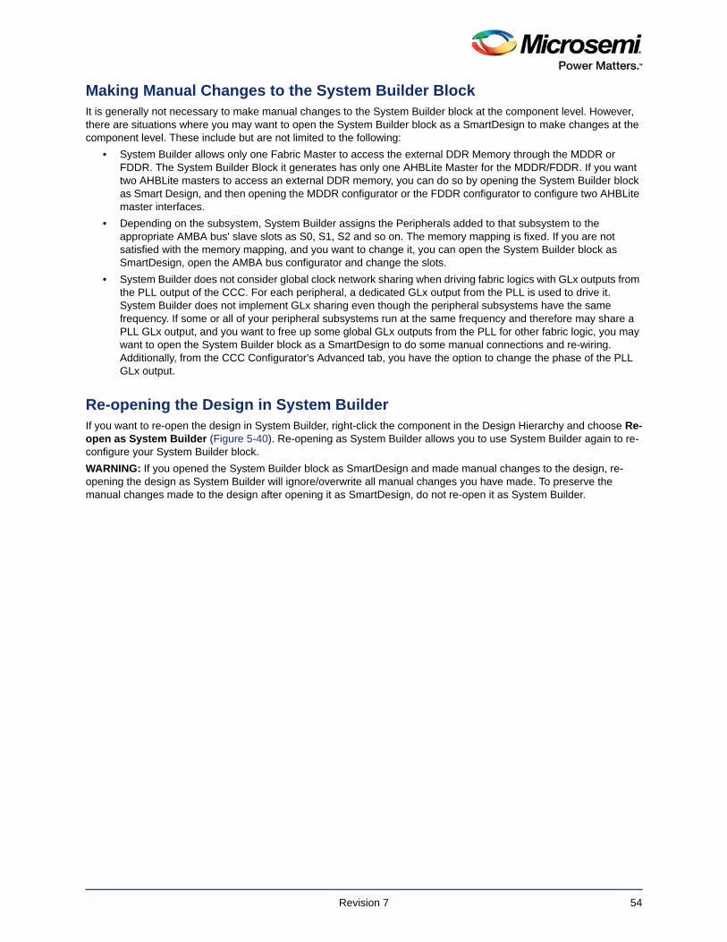
Making Manual Changes to the System Builder BlockIt is generally not necessary to make manual changes to the System Builder block at the component level. However, there are situations where you may want to open the System Builder block as a SmartDesign to make changes at the component level. These include but are not limited to the following:
• System Builder allows only one Fabric Master to access the external DDR Memory through the MDDR or FDDR. The System Builder Block it generates has only one AHBLite Master for the MDDR/FDDR. If you want two AHBLite masters to access an external DDR memory, you can do so by opening the System Builder block as Smart Design, and then opening the MDDR configurator or the FDDR configurator to configure two AHBLite master interfaces.
• Depending on the subsystem, System Builder assigns the Peripherals added to that subsystem to the appropriate AMBA bus' slave slots as S0, S1, S2 and so on. The memory mapping is fixed. If you are not satisfied with the memory mapping, and you want to change it, you can open the System Builder block as SmartDesign, open the AMBA bus configurator and change the slots.
• System Builder does not consider global clock network sharing when driving fabric logics with GLx outputs from the PLL output of the CCC. For each peripheral, a dedicated GLx output from the PLL is used to drive it. System Builder does not implement GLx sharing even though the peripheral subsystems have the same frequency. If some or all of your peripheral subsystems run at the same frequency and therefore may share a PLL GLx output, and you want to free up some global GLx outputs from the PLL for other fabric logic, you may want to open the System Builder block as a SmartDesign to do some manual connections and re-wiring. Additionally, from the CCC Configurator's Advanced tab, you have the option to change the phase of the PLL GLx output.
Re-opening the Design in System BuilderIf you want to re-open the design in System Builder, right-click the component in the Design Hierarchy and choose Re-open as System Builder (Figure 5-40). Re-opening as System Builder allows you to use System Builder again to re-configure your System Builder block.
WARNING: If you opened the System Builder block as SmartDesign and made manual changes to the design, re-opening the design as System Builder will ignore/overwrite all manual changes you have made. To preserve the manual changes made to the design after opening it as SmartDesign, do not re-open it as System Builder.
Revision 7 54
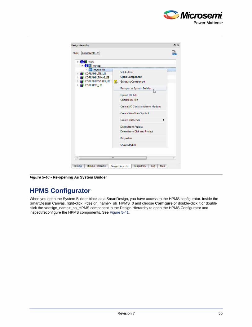
HPMS ConfiguratorWhen you open the System Builder block as a SmartDesign, you have access to the HPMS configurator. Inside the SmartDesign Canvas, right-click <design_name>_sb_HPMS_0 and choose Configure or double-click it or double click the <design_name>_sb_HPMS component in the Design Hierarchy to open the HPMS Configurator and inspect/reconfigure the HPMS components. See Figure 5-41.
Figure 5-40 • Re-opening As System Builder
Revision 7 55
Figure 5-41 • Accessing the HPMS Configurator
Revision 7 56
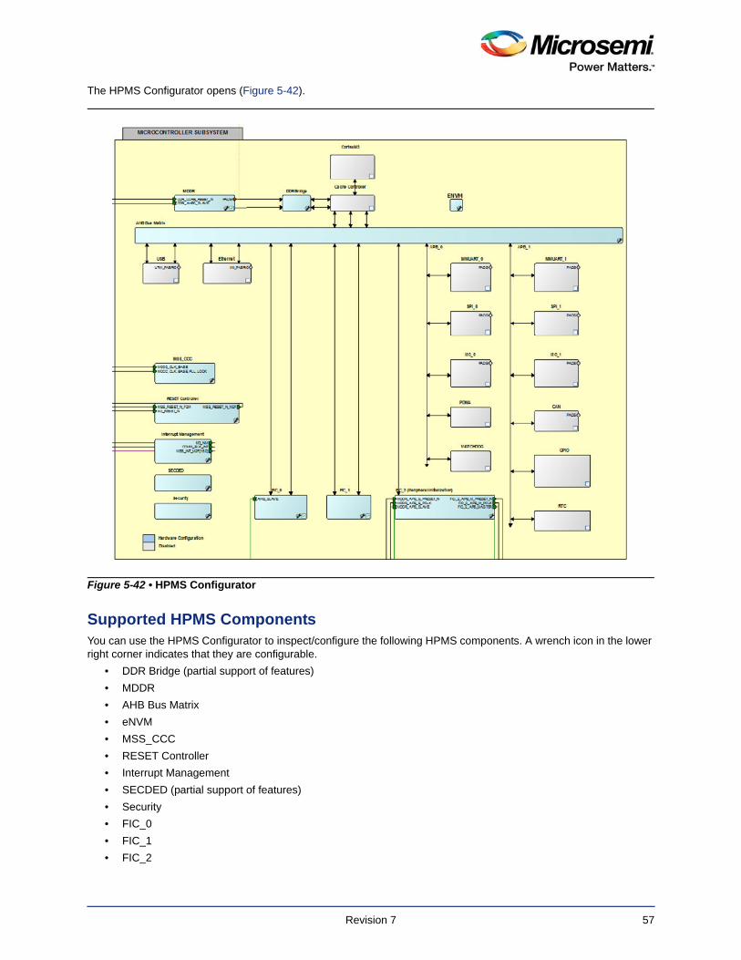
The HPMS Configurator opens (Figure 5-42).
Supported HPMS ComponentsYou can use the HPMS Configurator to inspect/configure the following HPMS components. A wrench icon in the lower right corner indicates that they are configurable.
• DDR Bridge (partial support of features)
• MDDR
• AHB Bus Matrix
• eNVM
• MSS_CCC
• RESET Controller
• Interrupt Management
• SECDED (partial support of features)
• Security
• FIC_0
• FIC_1
• FIC_2
Figure 5-42 • HPMS Configurator
Revision 7 57
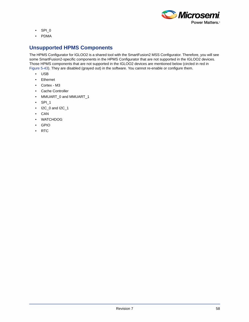
• SPI_0
• PDMA
Unsupported HPMS ComponentsThe HPMS Configurator for IGLOO2 is a shared tool with the SmartFusion2 MSS Configurator. Therefore, you will see some SmartFusion2-specific components in the HPMS Configurator that are not supported in the IGLOO2 devices. Those HPMS components that are not supported in the IGLOO2 devices are mentioned below (circled in red in Figure 5-43). They are disabled (grayed out) in the software. You cannot re-enable or configure them.
• USB
• Ethernet
• Cortex - M3
• Cache Controller
• MMUART_0 and MMUART_1
• SPI_1
• I2C_0 and I2C_1
• CAN
• WATCHDOG
• GPIO
• RTC
Revision 7 58
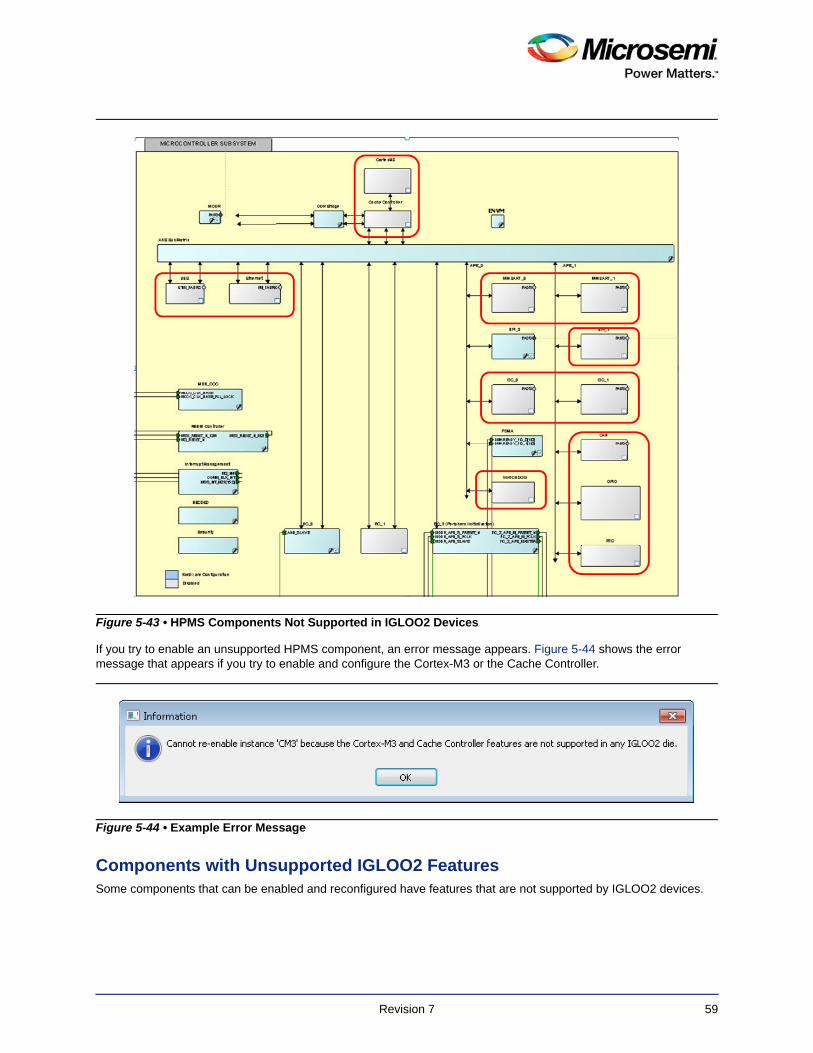
If you try to enable an unsupported HPMS component, an error message appears. Figure 5-44 shows the error message that appears if you try to enable and configure the Cortex-M3 or the Cache Controller.
Components with Unsupported IGLOO2 FeaturesSome components that can be enabled and reconfigured have features that are not supported by IGLOO2 devices.
Figure 5-43 • HPMS Components Not Supported in IGLOO2 Devices
Figure 5-44 • Example Error Message
Revision 7 59
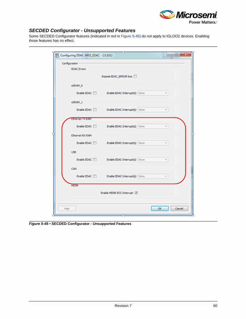
SECDED Configurator - Unsupported FeaturesSome SECDED Configurator features (indicated in red in Figure 5-45) do not apply to IGLOO2 devices. Enabling those features has no effect.
Figure 5-45 • SECDED Configurator - Unsupported Features
Revision 7 60
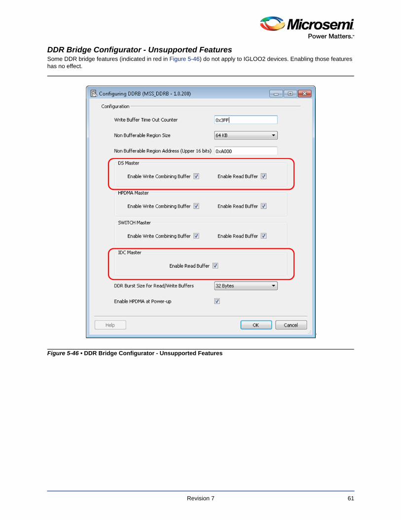
DDR Bridge Configurator - Unsupported FeaturesSome DDR bridge features (indicated in red in Figure 5-46) do not apply to IGLOO2 devices. Enabling those features has no effect.
Figure 5-46 • DDR Bridge Configurator - Unsupported Features
Revision 7 61
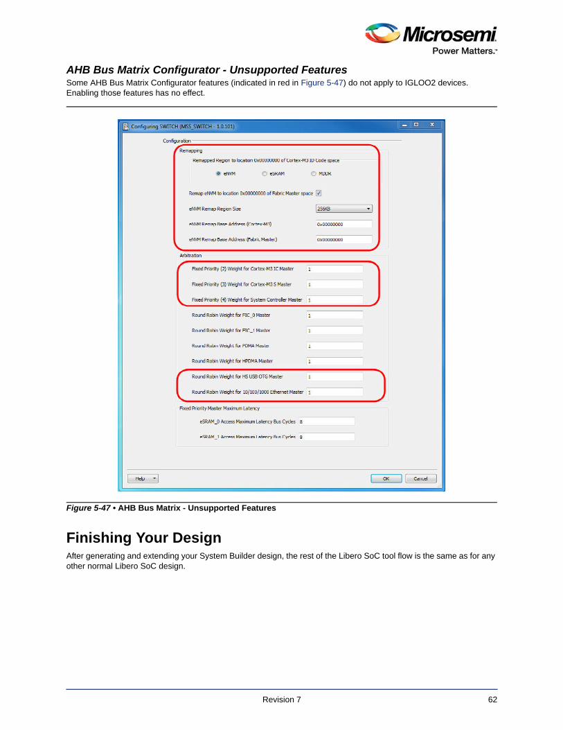
AHB Bus Matrix Configurator - Unsupported FeaturesSome AHB Bus Matrix Configurator features (indicated in red in Figure 5-47) do not apply to IGLOO2 devices. Enabling those features has no effect.
Finishing Your DesignAfter generating and extending your System Builder design, the rest of the Libero SoC tool flow is the same as for any other normal Libero SoC design.
Figure 5-47 • AHB Bus Matrix - Unsupported Features
Revision 7 62
A – Use Cases
System Builder has the flexibility to build different subsystems per your system and peripheral requirements. For each subsystem, the master may be the HPMS or a fabric master of an AMBA bus type you specify. The fabric slaves are configurable for different AMBA bus types of your choice. Different use cases/scenarios are listed to explain when, how and what subsystem to build for your design needs. For each subsystem, the memory mapping, base addresses and the AMBA bus configuration information is provided for you to write your HDL source files or user BFM files for simulation.
Use Case #1FIC0/1_Fabric_Master_Subystems with one or more AHBLite fabric masters and different types of slaves (AXI/AHBLite/APB3)
When to BuildYou build this subsystem if and when:
• You have one or more (up to a maximum of four) AHBLite fabric masters (either your own user HDL master, a SERDES master or any other master with AHBLite master BIF) which need to access the MSS space (eSRAM/eNVM/PDMA/HPDMA/SPI)
AND
• You want your AHBLite fabric master to master different fabric slaves.
Note: FIC_0 is available in all devices, whereas FIC_1 is available only in the larger devices.
How to BuildIn the System Builder Peripherals page:
1. Drag and drop (up to four) Fabric AMBA Master core(s) to the HPMS FIC_0/1 - Fabric Master Subsystem.
2. Configure them to be of type AHBLite. The HPMS component with its AHBLite slave BIF (FIC_0/1_AHB_SLAVE) will be an inherent slave to these fabric masters.
3. Drag and drop the generic Fabric AMBA Slave Cores to the same subsystem.
4. Configure the count and type (any of AHBLite/AXI/APB3). This will enable the fabric masters you have added earlier to master these fabric slaves.
Revision 7 63
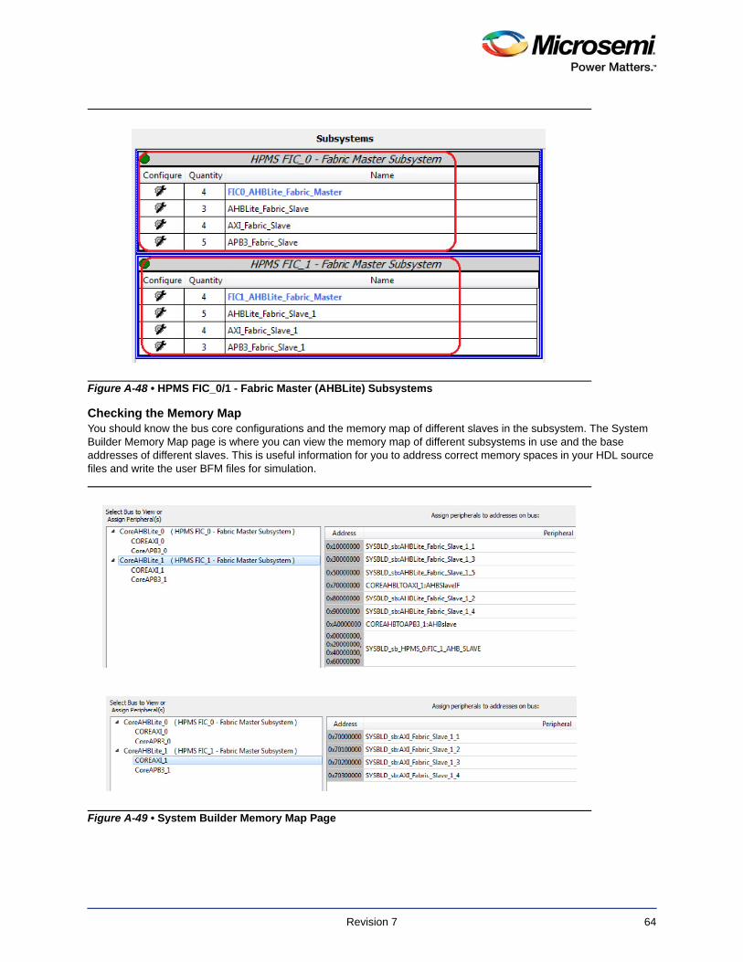
Checking the Memory MapYou should know the bus core configurations and the memory map of different slaves in the subsystem. The System Builder Memory Map page is where you can view the memory map of different subsystems in use and the base addresses of different slaves. This is useful information for you to address correct memory spaces in your HDL source files and write the user BFM files for simulation.
Figure A-48 • HPMS FIC_0/1 - Fabric Master (AHBLite) Subsystems
Figure A-49 • System Builder Memory Map Page
Revision 7 64
Understanding the Bus Core ConfigurationsAs shown in the memory map, the following is the bus core configuration (listed in hierarchical order):
• CoreAHBLite - Total 4GB space apportioned into 16 slave slots of 256MB each
– HPMS (FIC_0/1_AHB_SLAVE) is connected as an AHBLite slave to the combined region slave slot ofCoreAHBLite
– Other AHBLite fabric slaves are connected to the normal slave slots of CoreAHBLite
• CoreAXI - Total 16MB space apportioned into 16 slave slots of 1MB each
– AXI fabric slaves are connected to the slave slots of CoreAXI
• CoreAPB3 - Total 64KB space apportioned into 16 slave slots of 4KB each
– APB3 fabric slaves are connected to the slave slots of CoreAPB3
Making the Top Level Connections in SmartDesignFor all the generic Fabric AMBA Masters and Slaves you add to the HPMS FIC_0/1 - Fabric Master Subsystem, System Builder exposes the corresponding Master and Slave BIF ports of appropriate AMBA types with specified names on the System Builder interface. Connect your user fabric Masters and Slaves to appropriate BIF ports in the top level Smart Design component. You can also use the FIC_0/1_CLK and the HPMS_READY signals to drive your fabric logic's clock and reset inputs.
Revision 7 65
Use Case #2 FIC0/1_Fabric_Master_Subystems with one or more AXI fabric masters and different types of slaves (AXI/AHBLite/APB3)
When to BuildYou build this subsystem if and when:
• You have one or more AXI fabric masters (either your own user HDL masters, a SERDES master or any other masters with AXI master BIF) which need to access the HPMS space (eSRAM/eNVM/PDMA/SPI)
AND
• You also want your AXI fabric masters to master different fabric slaves.
Note: FIC_0 is available in all devices whereas FIC_1 is available only in the larger devices.
How to BuildIn the System Builder Peripherals page:
1. Drag and drop (up to four) Fabric AMBA Master core(s) to the HPMS FIC_0/1 - Fabric Master Subsystem.
2. Configure them to be of type AXI. The HPMS component with its AHBLite slave BIF (FIC_0/1_AHB_SLAVE) will be an inherent slave to these fabric masters (connected via CoreAXI --> CoreAXItoAHBL --> CoreAHBLite).
3. Drag and drop the generic Fabric AMBA Slaves to the same subsystem.
4. Configure their count and type (AHBLite/AXI/APB3). This will enable the fabric masters you have added earlier to master these fabric slaves.
Checking the Memory MapYou should know the bus core configurations and the memory map of different slaves in the subsystem. The System Builder Memory Map page is where you can view the memory map of different subsystems in use and the base addresses of different slaves. This is useful information for you to address correct memory spaces in your HDL source files and write the user BFM files for simulation.
Figure A-50 • HPMS FIC_0/1 Fabric Master (AXI) Subsystems
Revision 7 66
Figure A-51 • System Builder Memory Map Page
Revision 7 67
Understanding Bus Core ConfigurationsAs shown in the memory map, the following is the bus core configuration (listed in hierarchical order):
• CoreAXI - Total 4GB space apportioned into 16 slave slots of 256MB each
– CoreAHBLite is connected to the combined region slave slot of CoreAXI via CoreAXItoAHBL
– Other AXI fabric slaves are connected to the normal slave slots of CoreAXI
• CoreAHBLite - Total 256MB space apportioned into 16 slave slots of 16MB each
– HPMS (FIC_0/1_AHB_SLAVE) is connected to the slave slot 0 of CoreAHBLite
– Other AHBLite fabric slaves are connected to the other slave slots of CoreAHBLite
• CoreAPB3 - Total 64KB space apportioned into 16 slave slots of 4KB each
– APB3 fabric slaves are connected to the slave slots of CoreAPB3
Making the Connections in the Top Level SmartDesignFor all the generic Fabric AMBA Masters and Slaves added to the HPMS FIC_0/1 - Fabric Master Subsystem, System Builder exposes the corresponding Master and Slave BIF ports of appropriate types with specified names on the System Builder interface. Connect your user fabric Masters and Slaves to appropriate BIF ports in the top level Smart Design component. You can also use the FIC_0/1_CLK and the HPMS_READY signals to drive your fabric logic's clock and reset inputs.
Revision 7 68
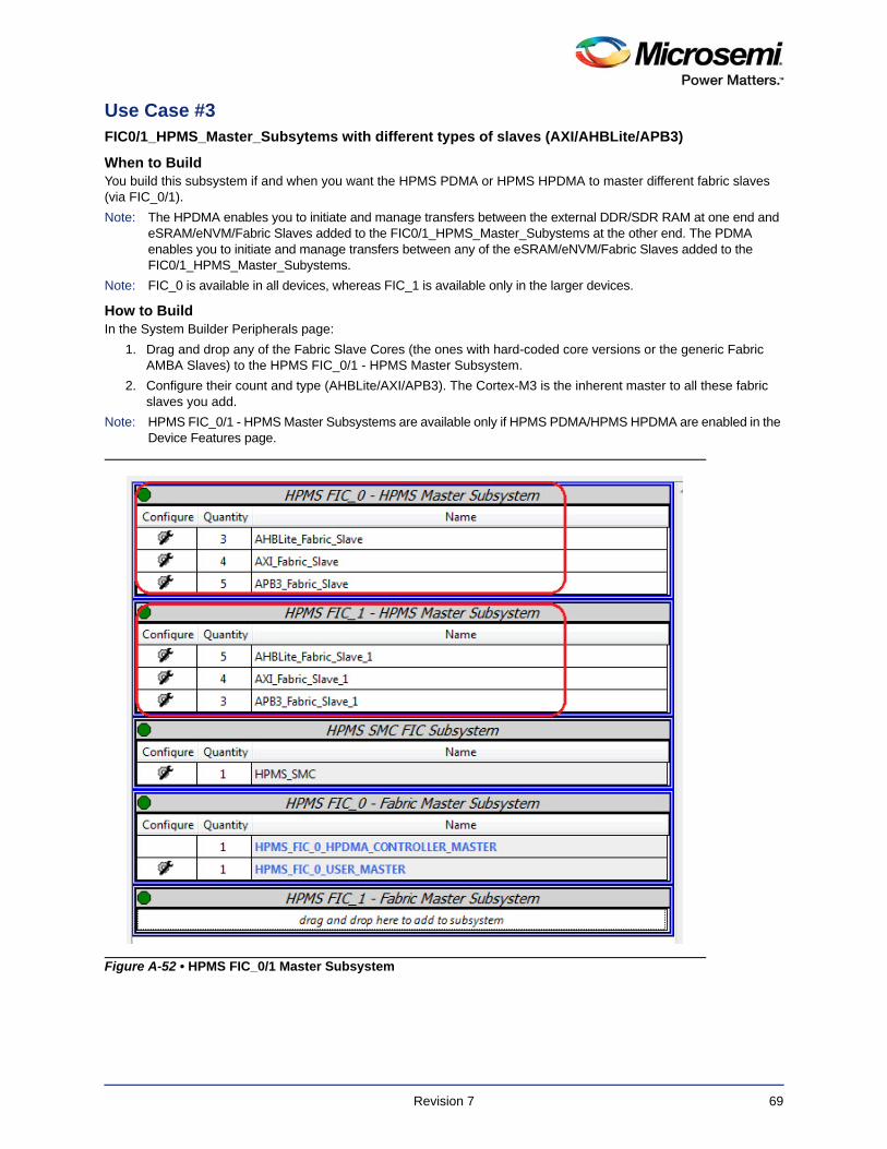
Use Case #3 FIC0/1_HPMS_Master_Subsytems with different types of slaves (AXI/AHBLite/APB3)
When to BuildYou build this subsystem if and when you want the HPMS PDMA or HPMS HPDMA to master different fabric slaves (via FIC_0/1).
Note: The HPDMA enables you to initiate and manage transfers between the external DDR/SDR RAM at one end and eSRAM/eNVM/Fabric Slaves added to the FIC0/1_HPMS_Master_Subystems at the other end. The PDMA enables you to initiate and manage transfers between any of the eSRAM/eNVM/Fabric Slaves added to the FIC0/1_HPMS_Master_Subystems.
Note: FIC_0 is available in all devices, whereas FIC_1 is available only in the larger devices.
How to Build In the System Builder Peripherals page:
1. Drag and drop any of the Fabric Slave Cores (the ones with hard-coded core versions or the generic Fabric AMBA Slaves) to the HPMS FIC_0/1 - HPMS Master Subsystem.
2. Configure their count and type (AHBLite/AXI/APB3). The Cortex-M3 is the inherent master to all these fabric slaves you add.
Note: HPMS FIC_0/1 - HPMS Master Subsystems are available only if HPMS PDMA/HPMS HPDMA are enabled in the Device Features page.
Figure A-52 • HPMS FIC_0/1 Master Subsystem
Revision 7 69

Checking the Memory MapYou should know the bus core configurations and the memory map of different slaves in the subsystem. The System Builder Memory Map page is where you can view the memory map of different subsystems in use and the base addresses of different slaves. This is useful information for you to configure PDMA/HPDMA configuration registers with appropriate source and destination addresses or address correct memory spaces in your HDL source files or write the user BFM files for simulation.
Revision 7 70
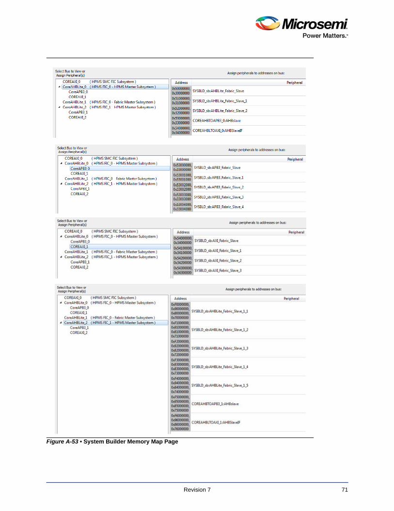
Figure A-53 • System Builder Memory Map Page
Revision 7 71
Understanding Bus Core ConfigurationsAs shown in the memory map, the following is the bus core configuration (listed in hierarchical order):
• CoreAHBLite - Total 256MB space apportioned into 16 slave slots of 16MB each
– The FIC_0/1_AHB_MASTER BIF of HPMS masters the CoreAHBLite and drives the upper 4 bits of theaddress based on whether it is FIC0 or FIC1
– AHBLite fabric slaves are connected to the slave slots of CoreAHBLite
• CoreAXI - Total 16MB space apportioned into 16 slave slots of 1MB each
– AXI fabric slaves are connected to the slave slots of CoreAXI
• CoreAPB3 - Total 64KB space apportioned into 16 slave slots of 4KB each
– APB3 fabric slaves are connected to the slave slots of CoreAPB3
Making the Top Level Connections in SmartDesignFor all the generic Fabric AMBA Slaves added to the HPMS FIC_0/1 - HPMS Master Subsystem, System Builder exposes the corresponding slave BIF ports of appropriate types with specified names on the System Builder interface. Connect your user fabric slaves to the appropriate BIF ports in the top level Smart Design component. You can also use the FIC_0/1_CLK and the HPMS_READY signals to drive your fabric logic's clock and reset inputs.
Revision 7 72
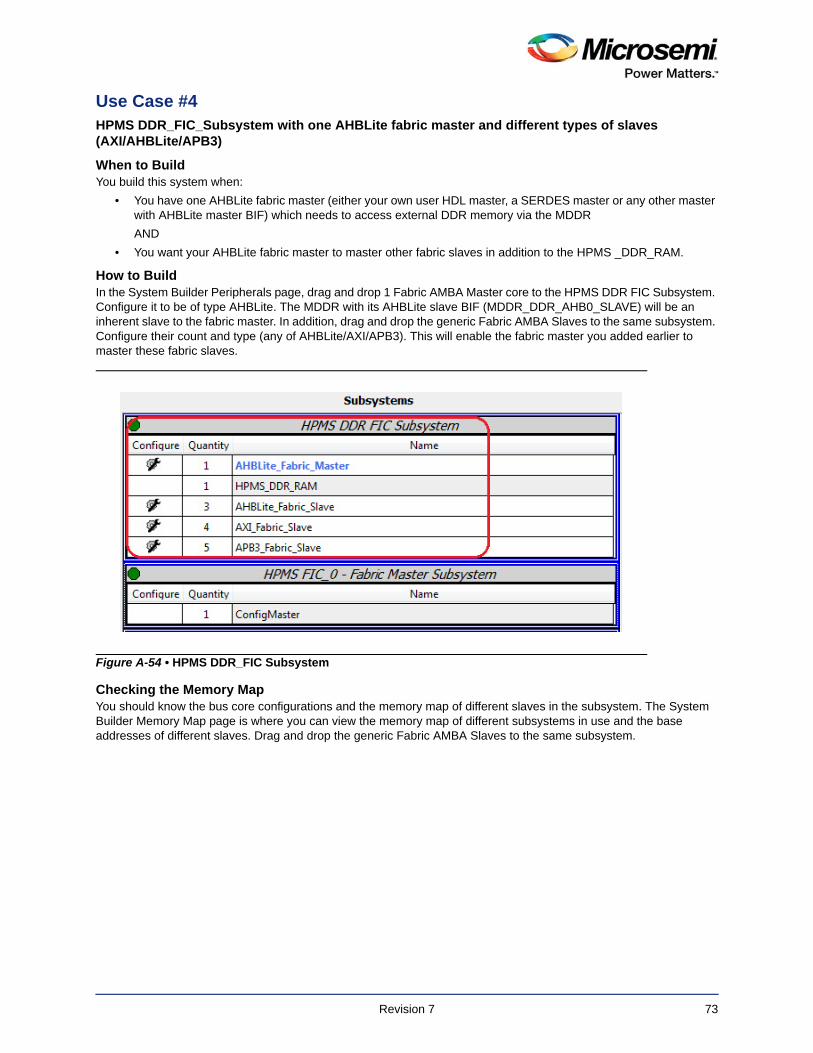
Use Case #4 HPMS DDR_FIC_Subsystem with one AHBLite fabric master and different types of slaves (AXI/AHBLite/APB3)
When to BuildYou build this system when:
• You have one AHBLite fabric master (either your own user HDL master, a SERDES master or any other master with AHBLite master BIF) which needs to access external DDR memory via the MDDR
AND
• You want your AHBLite fabric master to master other fabric slaves in addition to the HPMS _DDR_RAM.
How to BuildIn the System Builder Peripherals page, drag and drop 1 Fabric AMBA Master core to the HPMS DDR FIC Subsystem. Configure it to be of type AHBLite. The MDDR with its AHBLite slave BIF (MDDR_DDR_AHB0_SLAVE) will be an inherent slave to the fabric master. In addition, drag and drop the generic Fabric AMBA Slaves to the same subsystem. Configure their count and type (any of AHBLite/AXI/APB3). This will enable the fabric master you added earlier to master these fabric slaves.
Checking the Memory MapYou should know the bus core configurations and the memory map of different slaves in the subsystem. The System Builder Memory Map page is where you can view the memory map of different subsystems in use and the base addresses of different slaves. Drag and drop the generic Fabric AMBA Slaves to the same subsystem.
Figure A-54 • HPMS DDR_FIC Subsystem
Revision 7 73
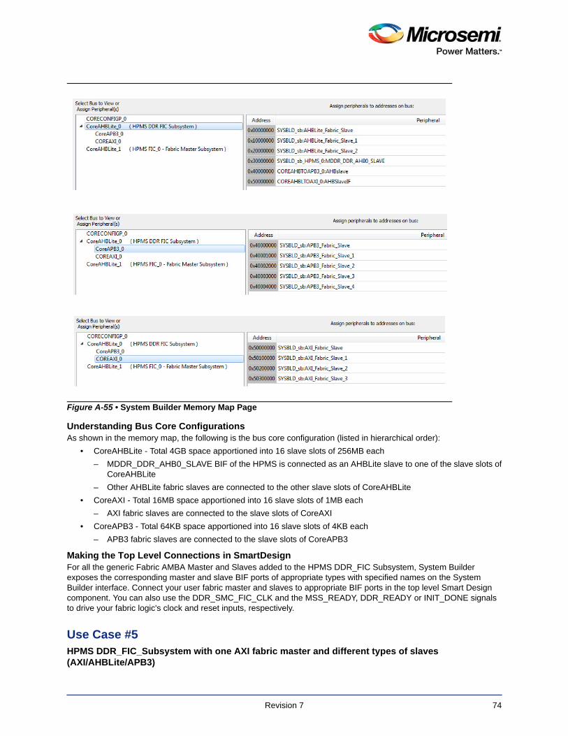
Understanding Bus Core ConfigurationsAs shown in the memory map, the following is the bus core configuration (listed in hierarchical order):
• CoreAHBLite - Total 4GB space apportioned into 16 slave slots of 256MB each
– MDDR_DDR_AHB0_SLAVE BIF of the HPMS is connected as an AHBLite slave to one of the slave slots ofCoreAHBLite
– Other AHBLite fabric slaves are connected to the other slave slots of CoreAHBLite
• CoreAXI - Total 16MB space apportioned into 16 slave slots of 1MB each
– AXI fabric slaves are connected to the slave slots of CoreAXI
• CoreAPB3 - Total 64KB space apportioned into 16 slave slots of 4KB each
– APB3 fabric slaves are connected to the slave slots of CoreAPB3
Making the Top Level Connections in SmartDesignFor all the generic Fabric AMBA Master and Slaves added to the HPMS DDR_FIC Subsystem, System Builder exposes the corresponding master and slave BIF ports of appropriate types with specified names on the System Builder interface. Connect your user fabric master and slaves to appropriate BIF ports in the top level Smart Design component. You can also use the DDR_SMC_FIC_CLK and the MSS_READY, DDR_READY or INIT_DONE signals to drive your fabric logic's clock and reset inputs, respectively.
Use Case #5HPMS DDR_FIC_Subsystem with one AXI fabric master and different types of slaves (AXI/AHBLite/APB3)
Figure A-55 • System Builder Memory Map Page
Revision 7 74
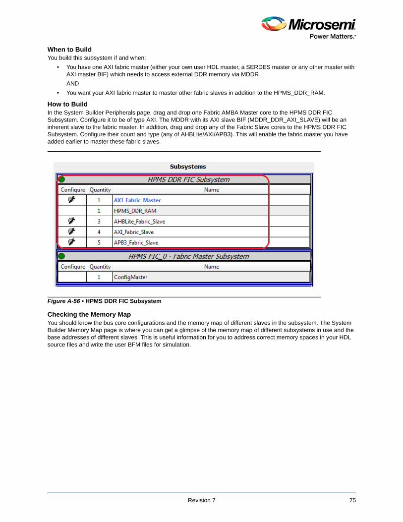
When to BuildYou build this subsystem if and when:
• You have one AXI fabric master (either your own user HDL master, a SERDES master or any other master with AXI master BIF) which needs to access external DDR memory via MDDR
AND
• You want your AXI fabric master to master other fabric slaves in addition to the HPMS_DDR_RAM.
How to BuildIn the System Builder Peripherals page, drag and drop one Fabric AMBA Master core to the HPMS DDR FIC Subsystem. Configure it to be of type AXI. The MDDR with its AXI slave BIF (MDDR_DDR_AXI_SLAVE) will be an inherent slave to the fabric master. In addition, drag and drop any of the Fabric Slave cores to the HPMS DDR FIC Subsystem. Configure their count and type (any of AHBLite/AXI/APB3). This will enable the fabric master you have added earlier to master these fabric slaves.
Checking the Memory MapYou should know the bus core configurations and the memory map of different slaves in the subsystem. The System Builder Memory Map page is where you can get a glimpse of the memory map of different subsystems in use and the base addresses of different slaves. This is useful information for you to address correct memory spaces in your HDL source files and write the user BFM files for simulation.
Figure A-56 • HPMS DDR FIC Subsystem
Revision 7 75
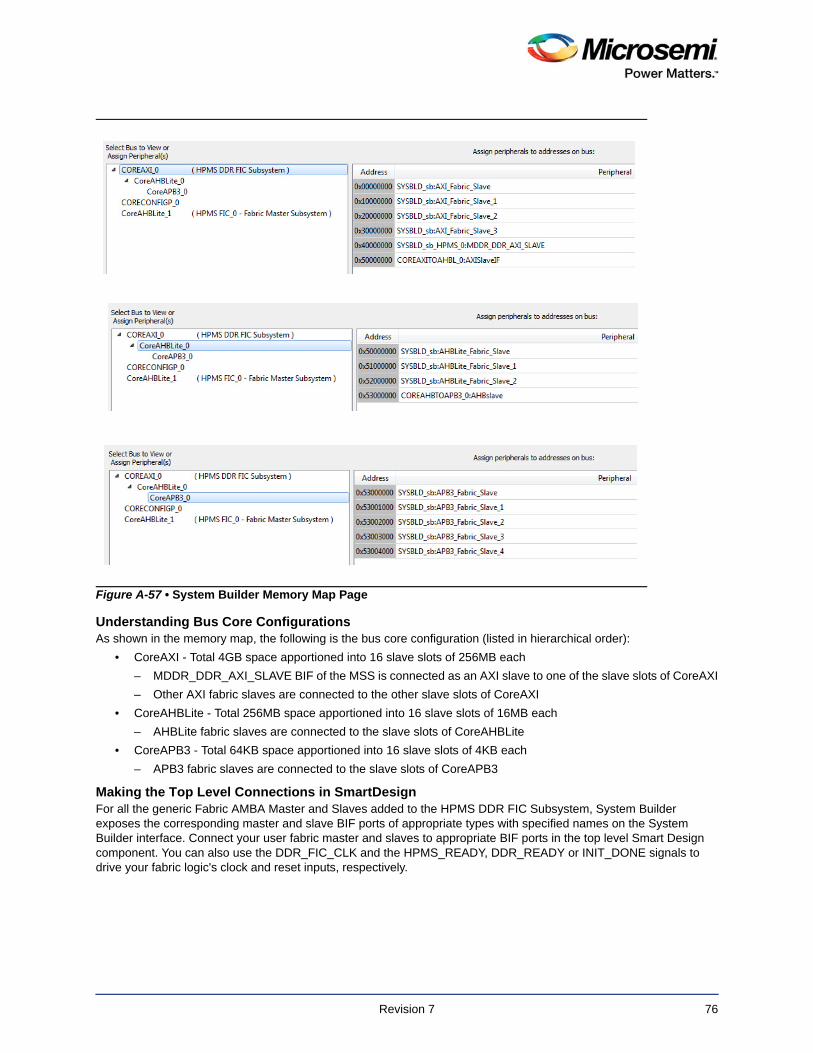
Understanding Bus Core ConfigurationsAs shown in the memory map, the following is the bus core configuration (listed in hierarchical order):
• CoreAXI - Total 4GB space apportioned into 16 slave slots of 256MB each
– MDDR_DDR_AXI_SLAVE BIF of the MSS is connected as an AXI slave to one of the slave slots of CoreAXI
– Other AXI fabric slaves are connected to the other slave slots of CoreAXI
• CoreAHBLite - Total 256MB space apportioned into 16 slave slots of 16MB each
– AHBLite fabric slaves are connected to the slave slots of CoreAHBLite
• CoreAPB3 - Total 64KB space apportioned into 16 slave slots of 4KB each
– APB3 fabric slaves are connected to the slave slots of CoreAPB3
Making the Top Level Connections in SmartDesignFor all the generic Fabric AMBA Master and Slaves added to the HPMS DDR FIC Subsystem, System Builder exposes the corresponding master and slave BIF ports of appropriate types with specified names on the System Builder interface. Connect your user fabric master and slaves to appropriate BIF ports in the top level Smart Design component. You can also use the DDR_FIC_CLK and the HPMS_READY, DDR_READY or INIT_DONE signals to drive your fabric logic's clock and reset inputs, respectively.
Figure A-57 • System Builder Memory Map Page
Revision 7 76
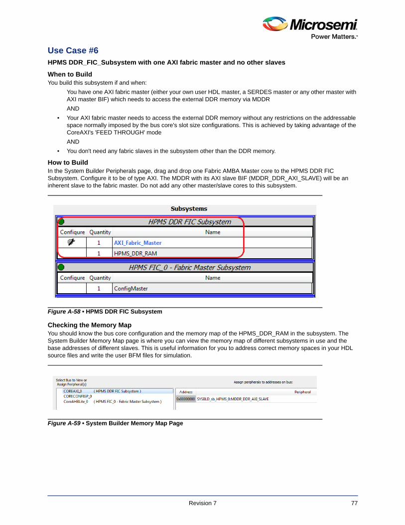
Use Case #6HPMS DDR_FIC_Subsystem with one AXI fabric master and no other slaves
When to BuildYou build this subsystem if and when:
You have one AXI fabric master (either your own user HDL master, a SERDES master or any other master with AXI master BIF) which needs to access the external DDR memory via MDDR
AND
• Your AXI fabric master needs to access the external DDR memory without any restrictions on the addressable space normally imposed by the bus core's slot size configurations. This is achieved by taking advantage of the CoreAXI's 'FEED THROUGH' mode
AND
• You don't need any fabric slaves in the subsystem other than the DDR memory.
How to BuildIn the System Builder Peripherals page, drag and drop one Fabric AMBA Master core to the HPMS DDR FIC Subsystem. Configure it to be of type AXI. The MDDR with its AXI slave BIF (MDDR_DDR_AXI_SLAVE) will be an inherent slave to the fabric master. Do not add any other master/slave cores to this subsystem.
Checking the Memory MapYou should know the bus core configuration and the memory map of the HPMS_DDR_RAM in the subsystem. The System Builder Memory Map page is where you can view the memory map of different subsystems in use and the base addresses of different slaves. This is useful information for you to address correct memory spaces in your HDL source files and write the user BFM files for simulation.
Figure A-58 • HPMS DDR FIC Subsystem
Figure A-59 • System Builder Memory Map Page
Revision 7 77
Understanding the Bus Core ConfigurationsAs shown in the memory map, the following is the bus core configuration (listed in hierarchical order):
• CoreAXI - Configured in 'FEED THROUGH' mode.
– FEED THROUGH' is like a direct wire connection where the CoreAXI's master BIF M0 is directly connectedto its slave BIF S0, without any restrictions of address space or slot sizes. This enables the AXI fabricmaster to access the external DDR memory space without any restrictions.
– MDDR_DDR_AXI_SLAVE BIF of the HPMS is connected as an AXI slave to the slave slot 0 of CoreAXI
Making the Top Level Connections in SmartDesignFor the generic Fabric AMBA Master added to the HPMS DDR FIC Subsystem, System Builder exposes the corresponding master BIF port on the System Builder interface. Connect your user fabric master to this BIF port in the top level Smart Design component. You can also use the DDR_FIC_CLK and the HPMS_READY, DDR_READY or INIT_DONE signals to drive your fabric logic's clock and reset inputs, respectively.
Revision 7 78
Use Case #7Fabric_DDR_Subsystem with one AHBLite fabric master and different types of slaves (AXI/AHBLite/APB3)
When to BuildYou build this system if and when:
• You have one AHBLite fabric master (either your own user HDL master, SERDES master or any other master with AHBLite master BIF) which needs to access external DDR memory via FDDR,
AND
• You want your AHBLite fabric master to master other fabric slaves in addition to the Fabric_DDR_RAM.
How to BuildIn the System Builder Peripherals page, drag and drop one Fabric AMBA Master core to the Fabric DDR Subsystem. Configure it to be of type AHBLite. The FDDR with its AHBLite slave BIF (AHB0_SLAVE) will be an inherent slave to the fabric master. In addition, drag and drop the generic Fabric AMBA Slaves to the same subsystem. Configure their count and type (any of AHBLite/AXI/APB3). This would enable the fabric master you have added earlier to master these fabric slaves.
Checking the Memory MapYou should know the bus core configurations and the memory map of different slaves in the subsystem. The System Builder Memory Map page is where you can get a glimpse of the memory map of different subsystems in use and the base addresses of different slaves. This is useful information for you to address correct memory spaces in your HDL
Figure A-60 • HPMS DDR FIC Subsystem
Revision 7 79
source files and write the user BFM files for simulation.This is useful information for you to write the user BFM files for simulation.
Understanding Bus Core ConfigurationsAs shown in the memory map, the following is the bus core configuration (listed in hierarchical order):
• CoreAHBLite - Total 4GB space apportioned into 16 slave slots of 256MB each
– AHB0_SLAVE BIF of the FDDR is connected as an AHBLite slave to one of the slave slots of CoreAHBLite
– Other AHBLite fabric slaves are connected to the other slave slots of CoreAHBLite
• CoreAXI - Total 16MB space apportioned into 16 slave slots of 1MB each
– AXI fabric slaves are connected to the slave slots of CoreAXI
• CoreAPB3 - Total 64KB space apportioned into 16 slave slots of 4KB each
– APB3 fabric slaves are connected to the slave slots of CoreAPB3
Making the Top Level Connections in SmartDesignFor all the generic Fabric AMBA Master and Slaves added to the Fabric DDR Subsystem, System Builder exposes the corresponding master and slave BIF ports of appropriate types with specified names on the System Builder interface. Connect your user fabric master and slaves to appropriate BIF ports in the top level Smart Design component. You can also use the FDDR_SUBSYSTEM_CLK and the HPMS_READY, DDR_READY or INIT_DONE signals to drive your fabric logic's clock and reset inputs, respectively.
Figure A-61 • System Builder Memory Map Page
Revision 7 80
Use Case #8Fabric_DDR_Subsystem with one AXI fabric master and different types of slaves (AXI/AHBLite/APB3)
When to BuildYou build this system if and when:
• You have one AXI fabric master (either your own user HDL master, a SERDES master or any other master with AXI master BIF) which needs to access external DDR memory via FDDR,.
AND
• You want your AXI fabric master to master other fabric slaves in addition to the Fabric_DDR_RAM.
How to BuildIn the System Builder Peripherals page, drag and drop one Fabric AMBA Master core to the Fabric DDR Subsystem. Configure it to be of type AXI. The FDDR with its AXI slave BIF (AXI_SLAVE) will be an inherent slave to the fabric master. Drag and drop any of the generic Fabric AMBA Slave cores to the Fabric DDR Subsystem, configure their count and type (any of AHBLite/AXI/APB3). This would enable the fabric master you have added earlier to master these fabric slaves.
Checking the Memory MapYou should know the bus core configurations and the memory map of different slaves in the subsystem. The System Builder Memory Map page is where you view the memory map of different subsystems in use and the base addresses
Figure A-62 • System Builder Fabric DDR Subsystem
Revision 7 81
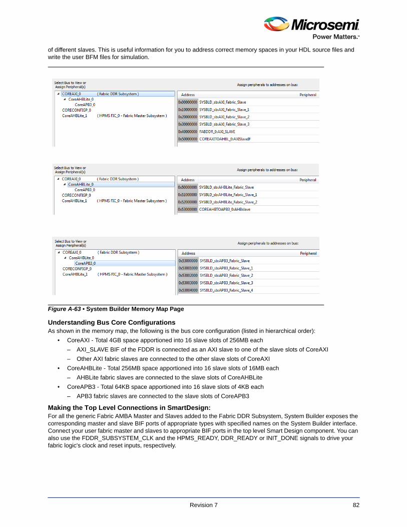
of different slaves. This is useful information for you to address correct memory spaces in your HDL source files and write the user BFM files for simulation.
Understanding Bus Core ConfigurationsAs shown in the memory map, the following is the bus core configuration (listed in hierarchical order):
• CoreAXI - Total 4GB space apportioned into 16 slave slots of 256MB each
– AXI_SLAVE BIF of the FDDR is connected as an AXI slave to one of the slave slots of CoreAXI
– Other AXI fabric slaves are connected to the other slave slots of CoreAXI
• CoreAHBLite - Total 256MB space apportioned into 16 slave slots of 16MB each
– AHBLite fabric slaves are connected to the slave slots of CoreAHBLite
• CoreAPB3 - Total 64KB space apportioned into 16 slave slots of 4KB each
– APB3 fabric slaves are connected to the slave slots of CoreAPB3
Making the Top Level Connections in SmartDesign:For all the generic Fabric AMBA Master and Slaves added to the Fabric DDR Subsystem, System Builder exposes the corresponding master and slave BIF ports of appropriate types with specified names on the System Builder interface. Connect your user fabric master and slaves to appropriate BIF ports in the top level Smart Design component. You can also use the FDDR_SUBSYSTEM_CLK and the HPMS_READY, DDR_READY or INIT_DONE signals to drive your fabric logic's clock and reset inputs, respectively.
Figure A-63 • System Builder Memory Map Page
Revision 7 82
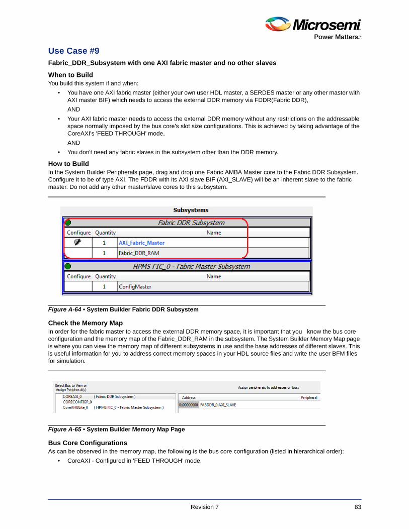
Use Case #9Fabric_DDR_Subsystem with one AXI fabric master and no other slaves
When to BuildYou build this system if and when:
• You have one AXI fabric master (either your own user HDL master, a SERDES master or any other master with AXI master BIF) which needs to access the external DDR memory via FDDR(Fabric DDR),
AND
• Your AXI fabric master needs to access the external DDR memory without any restrictions on the addressable space normally imposed by the bus core's slot size configurations. This is achieved by taking advantage of the CoreAXI's 'FEED THROUGH' mode,
AND
• You don't need any fabric slaves in the subsystem other than the DDR memory.
How to BuildIn the System Builder Peripherals page, drag and drop one Fabric AMBA Master core to the Fabric DDR Subsystem. Configure it to be of type AXI. The FDDR with its AXI slave BIF (AXI_SLAVE) will be an inherent slave to the fabric master. Do not add any other master/slave cores to this subsystem.
Check the Memory MapIn order for the fabric master to access the external DDR memory space, it is important that you know the bus core configuration and the memory map of the Fabric_DDR_RAM in the subsystem. The System Builder Memory Map page is where you can view the memory map of different subsystems in use and the base addresses of different slaves. This is useful information for you to address correct memory spaces in your HDL source files and write the user BFM files for simulation.
Bus Core ConfigurationsAs can be observed in the memory map, the following is the bus core configuration (listed in hierarchical order):
• CoreAXI - Configured in 'FEED THROUGH' mode.
Figure A-64 • System Builder Fabric DDR Subsystem
Figure A-65 • System Builder Memory Map Page
Revision 7 83
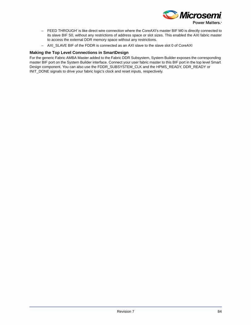
– FEED THROUGH' is like direct wire connection where the CoreAXI's master BIF M0 is directly connected toits slave BIF S0, without any restrictions of address space or slot sizes. This enabled the AXI fabric masterto access the external DDR memory space without any restrictions.
– AXI_SLAVE BIF of the FDDR is connected as an AXI slave to the slave slot 0 of CoreAXI
Making the Top Level Connections in SmartDesignFor the generic Fabric AMBA Master added to the Fabric DDR Subsystem, System Builder exposes the corresponding master BIF port on the System Builder interface. Connect your user fabric master to this BIF port in the top level Smart Design component. You can also use the FDDR_SUBSYSTEM_CLK and the HPMS_READY, DDR_READY or INIT_DONE signals to drive your fabric logic's clock and reset inputs, respectively.
Revision 7 84
B – Product Support
Microsemi SoC Products Group backs its products with various support services, including Customer Service, Customer Technical Support Center, a website, electronic mail, and worldwide sales offices. This appendix contains information about contacting Microsemi SoC Products Group and using these support services.
Customer ServiceContact Customer Service for non-technical product support, such as product pricing, product upgrades, update information, order status, and authorization.
From North America, call 800.262.1060From the rest of the world, call 650.318.4460Fax, from anywhere in the world, 650.318.8044
Customer Technical Support CenterMicrosemi SoC Products Group staffs its Customer Technical Support Center with highly skilled engineers who can help answer your hardware, software, and design questions about Microsemi SoC Products. The Customer Technical Support Center spends a great deal of time creating application notes, answers to common design cycle questions, documentation of known issues, and various FAQs. So, before you contact us, please visit our online resources. It is very likely we have already answered your questions.
Technical SupportFor Microsemi SoC Products Support, visit http://www.microsemi.com/products/fpga-soc/design-support/fpga-soc-support.
WebsiteYou can browse a variety of technical and non-technical information on the Microsemi SoC Products Group home page, at www.microsemi.com/soc.
Contacting the Customer Technical Support CenterHighly skilled engineers staff the Technical Support Center. The Technical Support Center can be contacted by email or through the Microsemi SoC Products Group website.
EmailYou can communicate your technical questions to our email address and receive answers back by email, fax, or phone. Also, if you have design problems, you can email your design files to receive assistance. We constantly monitor the email account throughout the day. When sending your request to us, please be sure to include your full name, company name, and your contact information for efficient processing of your request.
The technical support email address is [email protected].
85
MOCA
WOSaFa
E-
©2reloCosere
Microsemi makes no warranty, representation, or guarantee regarding the information contained herein orthe suitability of its products and services for any particular purpose, nor does Microsemi assume anyliability whatsoever arising out of the application or use of any product or circuit. The products soldhereunder and any other products sold by Microsemi have been subject to limited testing and should notbe used in conjunction with mission-critical equipment or applications. Any performance specifications arebelieved to be reliable but are not verified, and Buyer must conduct and complete all performance andother testing of the products, alone and together with, or installed in, any end-products. Buyer shall not relyon any data and performance specifications or parameters provided by Microsemi. It is the Buyer'sresponsibility to independently determine suitability of any products and to test and verify the same. Theinformation provided by Microsemi hereunder is provided "as is, where is" and with all faults, and the entirerisk associated with such information is entirely with the Buyer. Microsemi does not grant, explicitly orimplicitly, to any party any patent rights, licenses, or any other IP rights, whether with regard to such
About Microsemi
Microsemi Corporation (Nasdaq: MSCC) offers a comprehensive portfolio of semiconductorand system solutions for communications, defense & security, aerospace and industrialmarkets. Products include high-performance and radiation-hardened analog mixed-signalintegrated circuits, FPGAs, SoCs and ASICs; power management products; timing andsynchronization devices and precise time solutions, setting the world's standard for time; voiceprocessing devices; RF solutions; discrete components; Enterprise Storage andCommunication solutions, security technologies and scalable anti-tamper products; Ethernetsolutions; Power-over-Ethernet ICs and midspans; as well as custom design capabilities andservices. Microsemi is headquartered in Aliso Viejo, Calif. and has approximately 4,800employees globally. Learn more at www.microsemi.com.icrosemi Corporate Headquarters
ne Enterprise, Aliso Viejo, 92656 USA
ithin the USA: +1 (800) 713-4113 utside the USA: +1 (949) 380-6100les: +1 (949) 380-6136 x: +1 (949) 215-4996
mail: [email protected]
016 Microsemi Corporation. All rights served. Microsemi and the Microsemi go are trademarks of Microsemi rporation. All other trademarks and
My CasesMicrosemi SoC Products Group customers may submit and track technical cases online by going to My Cases.
Outside the U.S.Customers needing assistance outside the US time zones can either contact technical support via email ([email protected]) or contact a local sales office.
Visit About Us for sales office listings and corporate contacts.
Sales office listings can be found at www.microsemi.com/soc/company/contact/default.aspx.
ITAR Technical SupportFor technical support on RH and RT FPGAs that are regulated by International Traffic in Arms Regulations (ITAR), contact us via [email protected]. Alternatively, within My Cases, select Yes in the ITAR drop-down list. For a complete list of ITAR-regulated Microsemi FPGAs, visit the ITAR web page.
5-02-00488-7/03.16
information itself or anything described by such information. Information provided in this document isproprietary to Microsemi, and Microsemi reserves the right to make any changes to the information in thisdocument or to any products and services at any time without notice.
rvice marks are the property of their spective owners.