Embed Size (px)
Citation preview
DAC.COM KNOWLEDGE CENTER ARTICLE www.dac.com
This document has been submitted to, and reviewed and posted by, the editors of DAC.com. Please recycle if printed.
TSV-Aware 3D Physical Design Tool Needs for Faster Mainstream Acceptance of 3D ICs
Sung Kyu Lim School of Electrical and Computer Engineering
Georgia Institute of Technology, Atlanta,GA, USA
Notice of Copyright
This material is protected under the copyright laws of the U.S. and other countries and any uses not in conformity with the copyright laws are prohibited. Copyright for this document is held by the creator — authors and sponsoring organizations — of the material, all rights reserved.

DAC.COM KNOWLEDGE CENTER ARTICLE www.dac.com
Page 2 of 11
Article: Physical Design for 3D ICs TSV-Aware 3D Physical Design Tool Needs for Faster Mainstream Acceptance of 3D ICs
Sung Kyu Lim School of Electrical and Computer Engineering Georgia Institute of Technology, Atlanta,GA, USA
Abstract— This article presents several grand challenges in the area of physical design for through-silicon via (TSV) based 3D ICs. Most of these issues are centered around TSVs, which are a new element of the 3D IC layout. Fundamental understanding of the electrical, mechanical, and thermal properties of TSVs is essential in successful physical design of TSV-based 3D ICs. Further investigation of the impact of TSVs on the overall layout qualities such as performance, power, reliability, and manufacturability is crucial. As of early 2010, there is no commercial tool available for automatic placement and routing and sign-off analysis of timing, power, reliability, and manufacturability for TSV-based layouts. This calls for a concerted effort in developing such tools, which will have significant impact on the mainstream acceptance of TSV-based 3D IC technologies and products.
Index Terms— physical design for 3D ICs, through-silicon via (TSV), power and thermal management, design for manufacturability, 3D packaging.

DAC.COM KNOWLEDGE CENTER ARTICLE www.dac.com
Page 3 of 11
I. INTRODUCTION A major focus of the electronics industry today is to miniaturize ICs by advanced lithography
technologies, which is expected to continue to 22nm node and, perhaps, beyond. However, due to the increasing power, performance, and financial bottlenecks beyond 28nm, industry began to actively look for alternative solutions. This has led to the current focus on thinned and stacked 3D ICs, initially by wire-bond, later by flip-chip, and most recently by Through-Silicon Via (TSV). TSV provides the possibility of arranging digital and analog functional blocks across multiple dies at a very fine level of granularity, as illustrated in Figure 1. This results in a decrease in the overall wire length, which naturally translates into less wire delay and less power. Advances in 3D integration and packaging are undoubtedly gaining momentum and have become of critical interest to the semiconductor community.
Figure 1: (a) 2-tier 3D IC with face-to-face bonding, (b) top-down view of 2D vs 3D layout. (Source = reference [1].)
However, the lack of physical design tools that can handle TSVs and 3D die stacking delays the
mainstream acceptance of this technology. As of early 2010, the only commercial tool available for TSV-based 3D IC design is MAX-3D Layout Editor by Micro Magic, Inc [2]. This tool only supports layout editing for 3D ICs and does not offer automatic placement and routing. In addition, none of the commercial tools available for timing, power, signal integrity, power supply noise, and manufacturability analysis tools handles TSV and 3D stacking directly.
It is widely accepted that the most promising benefit of TSV-based 3D IC is wirelength and thus power and delay reduction enabled by the short vertical interconnect using TSVs. However, the sheer size of TSVs is identified as a major reason to discourage more usage of TSVs. According to the 2009 ITRS [3], TSV diameter is projected to range from 1.5um to 1.0um between 2009 and 2015. However, the area of a 4-transistor logic gate is projected to range from 0.82um2 to 0.20um2 during the same period. This means that the area ratio between TSVs and logic gates is projected to increase from 2.74 (= 2.25/0.82) to 5 (= 1.0/0.20). This TSV-to-gate-size ratio becomes even larger if the keep-out-zone around TSVs is considered, which is required to minimize manufacturability issues such as
DAC.COM KNOWLEDGE CENTER ARTICLE www.dac.com
Page 4 of 11
stress and lithography. Moreover, this wirelength issue—on which physical design has significant impact— directly influences the achievable performance-power tradeoff curves of 3D ICs. This calls for research that carefully considers the TSV size issue during partitioning, placement, routing, and clock tree synthesis stages of system physical implementation. Research is also needed to investigate the RC parasitics of these large TSVs and their impact on circuit power and performance. This article discusses seven grand challenges in the physical design research and tool development for TSV-based 3D ICs that are primarily stemming from TSVs, the latest challenging element in 3D IC layouts.
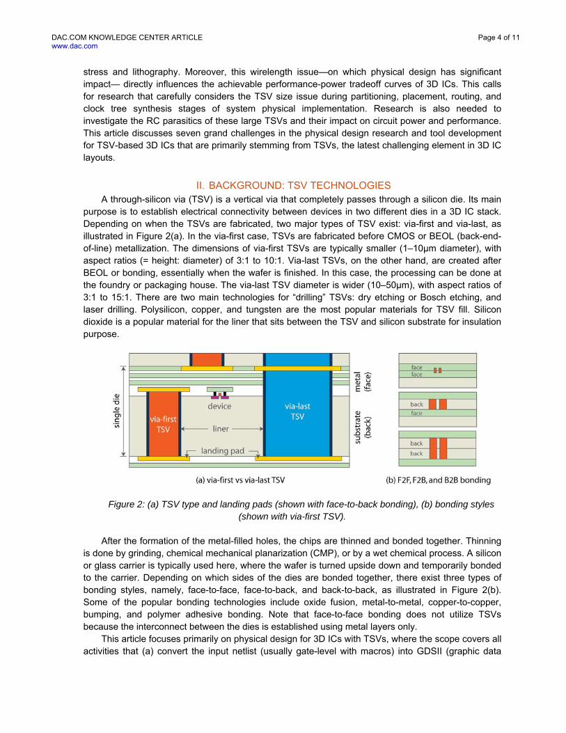
II. BACKGROUND: TSV TECHNOLOGIES A through-silicon via (TSV) is a vertical via that completely passes through a silicon die. Its main
purpose is to establish electrical connectivity between devices in two different dies in a 3D IC stack. Depending on when the TSVs are fabricated, two major types of TSV exist: via-first and via-last, as illustrated in Figure 2(a). In the via-first case, TSVs are fabricated before CMOS or BEOL (back-end-of-line) metallization. The dimensions of via-first TSVs are typically smaller (1–10μm diameter), with aspect ratios (= height: diameter) of 3:1 to 10:1. Via-last TSVs, on the other hand, are created after BEOL or bonding, essentially when the wafer is finished. In this case, the processing can be done at the foundry or packaging house. The via-last TSV diameter is wider (10–50μm), with aspect ratios of 3:1 to 15:1. There are two main technologies for “drilling” TSVs: dry etching or Bosch etching, and laser drilling. Polysilicon, copper, and tungsten are the most popular materials for TSV fill. Silicon dioxide is a popular material for the liner that sits between the TSV and silicon substrate for insulation purpose.
Figure 2: (a) TSV type and landing pads (shown with face-to-back bonding), (b) bonding styles (shown with via-first TSV).
After the formation of the metal-filled holes, the chips are thinned and bonded together. Thinning
is done by grinding, chemical mechanical planarization (CMP), or by a wet chemical process. A silicon or glass carrier is typically used here, where the wafer is turned upside down and temporarily bonded to the carrier. Depending on which sides of the dies are bonded together, there exist three types of bonding styles, namely, face-to-face, face-to-back, and back-to-back, as illustrated in Figure 2(b). Some of the popular bonding technologies include oxide fusion, metal-to-metal, copper-to-copper, bumping, and polymer adhesive bonding. Note that face-to-face bonding does not utilize TSVs because the interconnect between the dies is established using metal layers only.
This article focuses primarily on physical design for 3D ICs with TSVs, where the scope covers all activities that (a) convert the input netlist (usually gate-level with macros) into GDSII (graphic data

DAC.COM KNOWLEDGE CENTER ARTICLE www.dac.com
Page 5 of 11
system II) layouts, and (b) analyze the performance, power, reliability, manufacturability, and cost of the layouts. From the perspective of physical design, via-first TSVs are less intrusive because they interfere only with the device, M1, and top layers, whereas via-last TSVs interfere with all layers in the die as illustrated in Figure 2(a). Via-first TSVs have their landing pads on M1 and the top metal layers, whereas via-last TSVs have their landing pads only on the top metal layers. These landing pads include keep-out-zone uniformly located around them to reduce coupling effects. The connection between via-first TSVs are made using local interconnect and vias in between adjacent dies, whereas via-last TSVs are stacked on top of each other as illustrated in Figure 2(a). Therefore, via-first TSVs are usually used for signal and clock delivery, whereas power delivery network utilize via-last TSVs in general.
III. GRAND CHALLENGES IN THE PHYSICAL DESIGN FOR 3D ICS A. Grand Challenge #1: Pseudo 3D Tools and Their Limitations
One quick solution to the lack of physical design tools for 3D ICs is to build so-called “pseudo” 3D tools, which are based on “straightforward” 3D extension of existing tools for 2D ICs. These pseudo 3D tools are able to handle “simple” 3D designs, wherein existing 2D designs are simply stacked and connected without any major design change. A good example of this is 3D stacking of processor and memory dies, where the only change required is to add TSVs in the layouts to delivery signal, power, and clock in vertical directions. This can be done by adding TSVs in the layout whitepace or by slightly modifying the layout to leave space for TSVs and wires. These TSVs are then treated as pseudo IO pads in the layout.
However, future trends in 3D IC designs call for finer-grained 3D optimizations, such as 3D module floorplanning or 3D gate placement across the tiers for performance and power improvement; these optimizations in turn increase the TSV count. In addition, the number of tiers in the stack is expected to increase in order to meet the demand for higher-level system integration. This trend calls for more powerful, “native” 3D physical design tools that are built from ground up and are capable of handling many tiers and many TSVs simultaneously while addressing the current and emerging issues in reliability, cost, and manufacturability. In addition, TSV-aware 3D design verification and analysis tools including 3D DRC/LVS, timing, power, thermal, signal integrity, power integrity, and clock integrity analysis tools need to be seamlessly integrated and efficiently managed.
The newly published 2009 edition of the ITRS [3] added the following new metric that captures the physical design technology requirement for 3D IC: “percentage of native 3D physical design technology in TSV-based 3D IC implementation flow.” This metric today is around 10%, and is projected to increase. By 2025, all physical design tools used in 3D ICs are required to be “native 3D” to meet the demand for future 3D designs. “3D System Design Space Exploration Tools” and “Native 3D Power/Thermal Analysis and Optimization Tools” are specifically called out as potential solutions to meet this requirement.
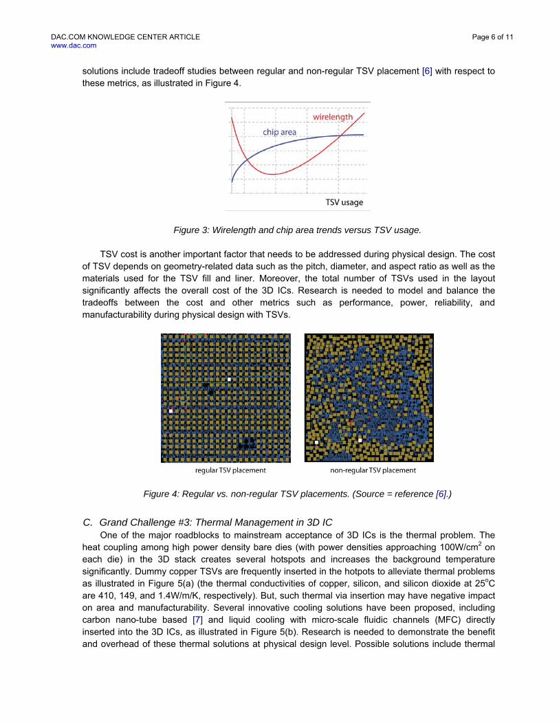
B. Grand Challenge #2: TSV Management, How Many and Where? TSV management is at the heart of physical design for 3D ICs. Especially, the count and location
of TSVs have significant impact on the quality and reliability of 3D IC layouts. A recent study [4] shows that the overall wirelength—up to a certain point—reduces as more TSVs are used in the 3D layout. However, mainly due to the large TSV size, wirelength begins to increase as the TSV count goes beyond this optimum point, as illustrated in Figure 3. The number of TSVs used in 3D IC layout entirely depends on how the design is partitioned into multiple dies. Research is needed to determine the optimal partitioning styles for given applications. Possible solutions include tradeoff studies among core-level, block-level, and gate-level partitioning across the dies in the 3D stack. Research is also required to investigate the impact of TSV location on 3D IC design quality and reliability [5]. Possible
DAC.COM KNOWLEDGE CENTER ARTICLE www.dac.com
Page 6 of 11
solutions include tradeoff studies between regular and non-regular TSV placement [6] with respect to these metrics, as illustrated in Figure 4.
Figure 3: Wirelength and chip area trends versus TSV usage. TSV cost is another important factor that needs to be addressed during physical design. The cost
of TSV depends on geometry-related data such as the pitch, diameter, and aspect ratio as well as the materials used for the TSV fill and liner. Moreover, the total number of TSVs used in the layout significantly affects the overall cost of the 3D ICs. Research is needed to model and balance the tradeoffs between the cost and other metrics such as performance, power, reliability, and manufacturability during physical design with TSVs.
Figure 4: Regular vs. non-regular TSV placements. (Source = reference [6].)
C. Grand Challenge #3: Thermal Management in 3D IC One of the major roadblocks to mainstream acceptance of 3D ICs is the thermal problem. The
heat coupling among high power density bare dies (with power densities approaching 100W/cm2 on each die) in the 3D stack creates several hotspots and increases the background temperature significantly. Dummy copper TSVs are frequently inserted in the hotpots to alleviate thermal problems as illustrated in Figure 5(a) (the thermal conductivities of copper, silicon, and silicon dioxide at 25oC are 410, 149, and 1.4W/m/K, respectively). But, such thermal via insertion may have negative impact on area and manufacturability. Several innovative cooling solutions have been proposed, including carbon nano-tube based [7] and liquid cooling with micro-scale fluidic channels (MFC) directly inserted into the 3D ICs, as illustrated in Figure 5(b). Research is needed to demonstrate the benefit and overhead of these thermal solutions at physical design level. Possible solutions include thermal

DAC.COM KNOWLEDGE CENTER ARTICLE www.dac.com
Page 7 of 11
TSV insertion during placement, and MFC-aware signal, power, and thermal interconnect planning and routing [8].
Figure 5: 3D IC cooling based on (a) thermal TSVs, (b) and liquid cooling with micro-fluidic channels. Dimensions are in microns. (Source = reference [8].)
D. Grand Challenge #4: Power Delivery in 3D IC One of the major challenges in 3D IC technology is on-chip power delivery. In 3D ICs, the on-chip
power-ground (P/G) networks in several tiers are vertically connected with P/G TSVs as illustrated in Figure 6, leading to much higher current demand per TSV. The number of TSVs used in the 3D P/G network is also limited so as to prevent placement and routing congestion. In addition, signal routing must be done carefully to prevent coupling noise between P/G TSVs and signal wires. This complex optimization problem usually results in larger area, more power consumption, and more noise, which leads to less performance and diminishing benefit of TSV-based 3D IC technology. Research is needed on P/G network synthesis, optimization, and analysis to addresses these issues while minimizing on-chip resource usage such as P/G wires, P/G TSVs, and on-chip decoupling capacitors.
Figure 6: (a) Power delivery network for a 3D IC, (b) IR-drop analysis.

DAC.COM KNOWLEDGE CENTER ARTICLE www.dac.com
Page 8 of 11
E. Grand Challenge #5: Clock Delivery in 3D IC The sequential elements in 3D ICs (i.e., flip-flops and latches) are potentially located in all of the
dies in the 3D stack. This poses a major challenge in delivering clock signal to all of them while reducing power consumption, skew, slew, and jitter. A recent study [9] shows that more clock TSV usage—up to a certain point—translates to more wirelength reduction and thus power saving, as illustrated in Figure 7. However, clock TSVs, as in the case with signal and P/G TSVs, occupy layout space and cause coupling. Thus, clock TSV management becomes an important issue in 3D clock tree synthesis. In addition, the high thermal variations in 3D ICs induce a substantial amount of skew variation in the clock tree, which has adverse implications for the performance and reliability of 3D ICs. The 3D clock tree itself is the longest wire in the circuit and contains many buffers to control skew and slew. Since the delay characteristics of clock wires, buffers, and TSVs are significantly affected by the temperature, care must be taken to ensure that the skew is kept minimum based on a given non-uniform thermal profile.
Figure 7: TSV usage vs. wirelength in 3D clock tree. (Source = reference [9].)
F. Grand Challenge #6: TSV-induced Design for Manufacturability Issues Primarily due to their large size compared with other layout objects, TSVs in 3D IC layouts cause
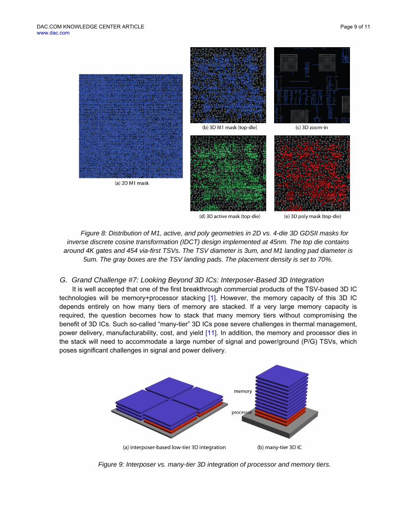
significantly non-uniform layout density distributions on the active, poly, and M1 layers, as illustrated in Figure 8. This density variation issue is expected to cause trouble during chemical-mechanical polishing (CMP) steps in the BEOL processing of the individual die, and requires new TSV-aware solutions. In addition, the printability of the devices and wires nearby TSVs will be affected in a non-negligible way. The CTE (coefficient of thermal expansion) mismatch between TSV copper (= 17.7 ppm/oC) and silicon (= 3.05 ppm/oC) causes significant stress to the devices nearby during manufacturing and operation of the 3D ICs. This in turn affects the timing characteristics of the devices and thus the overall circuit performance. The reliability of substrate and devices nearby TSVs is also affected because the thermal hotspots created in the regions cause repeated thermal expansion and contraction during 3D IC operation. This transient thermal behavior, together with the residual stress from TSV fabrication, may cause cracking and other physical damage in the substrate and devices. Research is required to address these issues during physical design. Possible solutions include TSV-aware CMP fill synthesis for the top and bottom metal layers, TSV stress-aware timing analysis and physical design [10], and TSV-aware substrate and device reliability modeling and optimization.
DAC.COM KNOWLEDGE CENTER ARTICLE www.dac.com
Page 9 of 11
Figure 8: Distribution of M1, active, and poly geometries in 2D vs. 4-die 3D GDSII masks for inverse discrete cosine transformation (IDCT) design implemented at 45nm. The top die contains
around 4K gates and 454 via-first TSVs. The TSV diameter is 3um, and M1 landing pad diameter is 5um. The gray boxes are the TSV landing pads. The placement density is set to 70%.
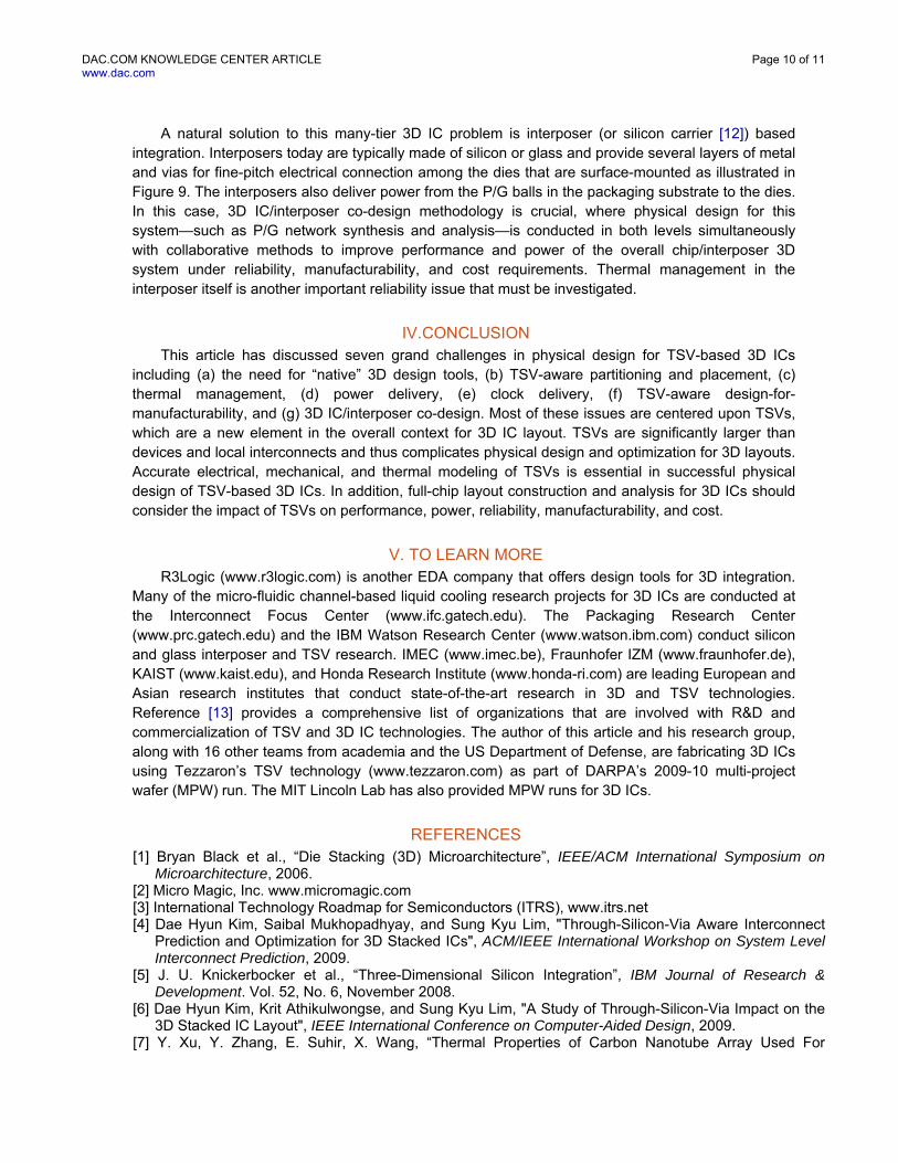
G. Grand Challenge #7: Looking Beyond 3D ICs: Interposer-Based 3D Integration It is well accepted that one of the first breakthrough commercial products of the TSV-based 3D IC
technologies will be memory+processor stacking [1]. However, the memory capacity of this 3D IC depends entirely on how many tiers of memory are stacked. If a very large memory capacity is required, the question becomes how to stack that many memory tiers without compromising the benefit of 3D ICs. Such so-called “many-tier” 3D ICs pose severe challenges in thermal management, power delivery, manufacturability, cost, and yield [11]. In addition, the memory and processor dies in the stack will need to accommodate a large number of signal and power/ground (P/G) TSVs, which poses significant challenges in signal and power delivery.
Figure 9: Interposer vs. many-tier 3D integration of processor and memory tiers.
DAC.COM KNOWLEDGE CENTER ARTICLE www.dac.com
Page 10 of 11
A natural solution to this many-tier 3D IC problem is interposer (or silicon carrier [12]) based
integration. Interposers today are typically made of silicon or glass and provide several layers of metal and vias for fine-pitch electrical connection among the dies that are surface-mounted as illustrated in Figure 9. The interposers also deliver power from the P/G balls in the packaging substrate to the dies. In this case, 3D IC/interposer co-design methodology is crucial, where physical design for this system—such as P/G network synthesis and analysis—is conducted in both levels simultaneously with collaborative methods to improve performance and power of the overall chip/interposer 3D system under reliability, manufacturability, and cost requirements. Thermal management in the interposer itself is another important reliability issue that must be investigated.
IV. CONCLUSION This article has discussed seven grand challenges in physical design for TSV-based 3D ICs
including (a) the need for “native” 3D design tools, (b) TSV-aware partitioning and placement, (c) thermal management, (d) power delivery, (e) clock delivery, (f) TSV-aware design-for-manufacturability, and (g) 3D IC/interposer co-design. Most of these issues are centered upon TSVs, which are a new element in the overall context for 3D IC layout. TSVs are significantly larger than devices and local interconnects and thus complicates physical design and optimization for 3D layouts. Accurate electrical, mechanical, and thermal modeling of TSVs is essential in successful physical design of TSV-based 3D ICs. In addition, full-chip layout construction and analysis for 3D ICs should consider the impact of TSVs on performance, power, reliability, manufacturability, and cost.
V. TO LEARN MORE R3Logic (www.r3logic.com) is another EDA company that offers design tools for 3D integration.
Many of the micro-fluidic channel-based liquid cooling research projects for 3D ICs are conducted at the Interconnect Focus Center (www.ifc.gatech.edu). The Packaging Research Center (www.prc.gatech.edu) and the IBM Watson Research Center (www.watson.ibm.com) conduct silicon and glass interposer and TSV research. IMEC (www.imec.be), Fraunhofer IZM (www.fraunhofer.de), KAIST (www.kaist.edu), and Honda Research Institute (www.honda-ri.com) are leading European and Asian research institutes that conduct state-of-the-art research in 3D and TSV technologies. Reference [13] provides a comprehensive list of organizations that are involved with R&D and commercialization of TSV and 3D IC technologies. The author of this article and his research group, along with 16 other teams from academia and the US Department of Defense, are fabricating 3D ICs using Tezzaron’s TSV technology (www.tezzaron.com) as part of DARPA’s 2009-10 multi-project wafer (MPW) run. The MIT Lincoln Lab has also provided MPW runs for 3D ICs.
REFERENCES [1] Bryan Black et al., “Die Stacking (3D) Microarchitecture”, IEEE/ACM International Symposium on
Microarchitecture, 2006. [2] Micro Magic, Inc. www.micromagic.com [3] International Technology Roadmap for Semiconductors (ITRS), www.itrs.net [4] Dae Hyun Kim, Saibal Mukhopadhyay, and Sung Kyu Lim, "Through-Silicon-Via Aware Interconnect
Prediction and Optimization for 3D Stacked ICs", ACM/IEEE International Workshop on System Level Interconnect Prediction, 2009.
[5] J. U. Knickerbocker et al., “Three-Dimensional Silicon Integration”, IBM Journal of Research & Development. Vol. 52, No. 6, November 2008.
[6] Dae Hyun Kim, Krit Athikulwongse, and Sung Kyu Lim, "A Study of Through-Silicon-Via Impact on the 3D Stacked IC Layout", IEEE International Conference on Computer-Aided Design, 2009.
[7] Y. Xu, Y. Zhang, E. Suhir, X. Wang, “Thermal Properties of Carbon Nanotube Array Used For

DAC.COM KNOWLEDGE CENTER ARTICLE www.dac.com
Page 11 of 11
Integrated Circuit Cooling”, Journal of Applied Physics, Volume 100, Issue 7, 2006. [8] Young-Joon Lee, Rohan Goel, and Sung Kyu Lim, "Multi-Functional Interconnect Co-optimization for
Fast and Reliable 3D Stacked ICs", IEEE International Conference on Computer-Aided Design, 2009. [9] Xin Zhao, Dean Lewis, Hsien-Hsin S. Lee, and Sung Kyu Lim, "Pre-Bond Testable Low-Power Clock
Tree Design for 3D Stacked ICs", IEEE International Conference on Computer-Aided Design, 2009. [10] Jae-seok Yang, Krit Athikulwongse, Young-Joon Lee, Sung Kyu Lim, and David Pan, “TSV Stress
Aware Timing Analysis with Applications to 3D-IC Layout Optimization”, ACM Design Automation Conference, 2010.
[11] Michael Healy and Sung Kyu Lim, "A Study of Stacking Limit and Scaling in 3D ICs: an Interconnect Perspective", IEEE Electronic Components and Technology Conference, 2009.
[12] P. S. Andry, C. K. Tsang, B. C. Webb, E. J. Sprogis, S. L. Wright, B. Dang, and D. G. Manzer, “Fabrication and Characterization of Robust Through-Silicon Vias for Silicon-Carrier Applications”, IBM Journal of Research and Development. Vol. 52, No. 6, November 2008.
[13] 3D IC Industry Summary, www.tezzaron.com/technology/3D_IC_Summary.html