Embed Size (px)
Citation preview

www.ti.com
FEATURES APPLICATIONS
IN2
VSSOP PACKAGE(TOP VIEW)
1
2
3
4
5
10
9
8
7
6
IN1
NO1
GND
NO2
V+
NC1
COM1
NC2
COM2
DESCRIPTION
TS5A231600.9-Ω DUAL SPDT ANALOG SWITCH
5-V/3.3-V 2-CHANNEL 2:1 MULTIPLEXER/DEMULTIPLEXERSCDS210A–AUGUST 2005–REVISED APRIL 2006
• Cell Phones• Specified Make-Before-Break Switching• PDAs• Low ON-State Resistance (1 Ω)• Portable Instrumentation• Control Inputs Are 5.5-V Tolerant• Audio and Video Signal Routing• Low Charge Injection• Low-Voltage Data Acquisition Systems• Excellent ON-State Resistance Matching• Communication Circuits• Low Total Harmonic Distortion (THD)• Modems
• 1.65-V to 5.5-V Single-Supply Operation • Hard Drives• Latch-Up Performance Exceeds 100 mA Per • Computer Peripherals
JESD 78, Class II• Wireless Terminals and Peripherals
• ESD Performance Tested Per JESD 22– 2000-V Human-Body Model
(A114-B, Class II)– 1000-V Charged-Device Model (C101)
The TS5A23160 is a dual single-pole double-throw (SPDT) analog switch that is designed to operate from1.65 V to 5.5 V. The device offers a low ON-state resistance and an excellent channel-to-channel ON-stateresistance matching. The device has excellent total harmonic distortion (THD) performance and consumes verylow power. These features make this device suitable for portable audio applications.
FUNCTION TABLE
NC TO COM, NO TO COM,IN COM TO NC COM TO NO
L ON OFF
H OFF ON
Please be aware that an important notice concerning availability, standard warranty, and use in critical applications of TexasInstruments semiconductor products and disclaimers thereto appears at the end of this data sheet.
PRODUCTION DATA information is current as of publication date. Copyright © 2005–2006, Texas Instruments IncorporatedProducts conform to specifications per the terms of the TexasInstruments standard warranty. Production processing does notnecessarily include testing of all parameters.

www.ti.com
TS5A231600.9-Ω DUAL SPDT ANALOG SWITCH5-V/3.3-V 2-CHANNEL 2:1 MULTIPLEXER/DEMULTIPLEXERSCDS210A–AUGUST 2005–REVISED APRIL 2006
SUMMARY OF CHARACTERISTICS (1)
Dual 2:1 Multiplexer/Configuration Demultiplexer
(2 × SPDT)
Number of channels 2
ON-state resistance (ron) 0.9 Ω
ON-state resistance match (∆ron) 0.1 Ω
ON-state resistance flatness 0.15 Ω(ron(flat))
Turn-on/turn-off time (tON/tOFF) 2.5 ns/6 ns
Make-before-break time (tMBB) 5.5 ns
Charge injection (QC) 1 pC
Bandwidth (BW) 95 MHz
OFF isolation (OISO) –64 dB at 1 MHz
Crosstak (XTALK) –64 dB at 1 MHz
Total harmonic distortion (THD) 0.004%
Leakage current (INC(OFF)) ±20 nA
Power-supply current (I+) 0.1 µA
Package option 10-pin VSSOP
(1) V+ = 5 V, TA = 25°C
ORDERING INFORMATION
TA PACKAGE (1) ORDERABLE PART NUMBER TOP-SIDE MARKING
–40°C to 85°C VSSOP – DGS (MSOP) Tape and reel TS5A23160DGSR PREVIEW
(1) Package drawings, standard packing quantities, thermal data, symbolization, and PCB design guidelines are available atwww.ti.com/sc/package.
2 Submit Documentation Feedback

www.ti.com
Absolute Maximum Ratings (1) (2)
TS5A231600.9-Ω DUAL SPDT ANALOG SWITCH
5-V/3.3-V 2-CHANNEL 2:1 MULTIPLEXER/DEMULTIPLEXERSCDS210A–AUGUST 2005–REVISED APRIL 2006
over operating free-air temperature range (unless otherwise noted)
MIN MAX UNIT
V+ Supply voltage range (3) –0.5 6.5 V
VNCVNO Analog voltage range (3) (4) (5) –0.5 V+ + 0.5 VVCOM
IK Analog port diode current VNC, VNO, VCOM < 0 or VNC, VNO, VCOM > V+ –50 50 mA
INC On-state switch current –200 200INO VNC, VNO, VCOM = 0 to V+ mA
On-state peak switch current (6) –400 400ICOM
VI Digital input voltage range (3) (4) –0.5 6.5 V
IIK Digital input clamp current VI < 0 –50 mA
I+ Continuous current through V+ 100 mA
IGND Continuous current through GND –100 100 mA
θJA Package thermal impedance (7) 165 °C/W
Tstg Storage temperature range –65 150 °C
(1) Stresses above these ratings may cause permanent damage. Exposure to absolute maximum conditions for extended periods maydegrade device reliability. These are stress ratings only, and functional operation of the device at these or any other conditions beyondthose specified is not implied.
(2) The algebraic convention, whereby the most negative value is a minimum and the most positive value is a maximum(3) All voltages are with respect to ground, unless otherwise specified.(4) The input and output voltage ratings may be exceeded if the input and output clamp-current ratings are observed.(5) This value is limited to 5.5 V maximum.(6) Pulse at 1-ms duration < 10% duty cycle(7) The package thermal impedance is calculated in accordance with JESD 51-7.
3Submit Documentation Feedback

www.ti.com
Electrical Characteristics for 5-V Supply (1)
TS5A231600.9-Ω DUAL SPDT ANALOG SWITCH5-V/3.3-V 2-CHANNEL 2:1 MULTIPLEXER/DEMULTIPLEXERSCDS210A–AUGUST 2005–REVISED APRIL 2006
V+ = 4.5 V to 5.5 V, TA = –40°C to 85°C (unless otherwise noted)
PARAMETER SYMBOL TEST CONDITIONS TA V+ MIN TYP MAX UNIT
Analog Switch
Analog signal VCOM, VNO, 0 V+ Vrange VNC
25°C 0.8 1.1Peak ON 0 ≤ (VNO or VNC) ≤ V+, Switch ON,rpeak 4.5 V Ωresistance ICOM = –100 mA, See Figure 14 Full 1.5
25°C 0.7 0.9ON-state VNO or VNC = 2.5 V, Switch ON,ron 4.5 V Ωresistance ICOM = –100 mA, See Figure 14 Full 1.1
ON-state 25°C 0.05 0.1resistance VNO or VNC = 2.5 V, Switch ON,match ∆ron 4.5 V ΩICOM = –100 mA, See Figure 14 Full 0.1betweenchannels
0 ≤ (VNO or VNC) ≤ V+, Switch ON, 25°C 0.15ICOM = –100 mA, See Figure 14ON-stateresistance ron(flat) 4.5 V ΩVNO or VNC = 1 V, 25°C 0.1 0.25Switch ON,flatness 1.5 V, 2.5 V, See Figure 14 Full 0.25ICOM = –100 mA,
VNC or VNO = 1 V, 25°C –20 2 20VCOM = 4.5 V,INC(OFF), Switch OFF,or 5.5 V nANC, NO INO(OFF) See Figure 15 Full –150 150VNC or VNO = 4.5 V,OFF leakageVCOM = 1 V,current
25°C –1 1INC(PWROFF), VNC or VNO = 0 to 5.5 V, Switch OFF, 0 V µAINO(PWROFF) VCOM = 5.5 V to 0, See Figure 15 Full –20 20
VNC or VNO = 1 V, 25°C –20 20NC, NO INC(ON), VCOM = Open, Switch ON,ON leakage 5.5 V nAINO(ON) VNC or VNO = 4.5 V, See Figure 16 Full –150 150current VCOM = Open,
COM 25°C –1 0.1 1VNC or VNO = 0 to 5.5 V, Switch OFF,OFF leakage ICOM(PWROFF) 0 V µAVCOM = 5.5 V to 0, See Figure 15 Full –20 20current
VNC or VNO = Open, 25°C –20 2 20COM VCOM = 1 V, Switch ON,ON leakage ICOM(ON) 5.5 V nAVNC or VNO = Open, See Figure 16 Full –150 150current VCOM = 4.5 V,
(1) The algebraic convention, whereby the most negative value is a minimum and the most positive value is a maximum
4 Submit Documentation Feedback

www.ti.com
TS5A231600.9-Ω DUAL SPDT ANALOG SWITCH
5-V/3.3-V 2-CHANNEL 2:1 MULTIPLEXER/DEMULTIPLEXERSCDS210A–AUGUST 2005–REVISED APRIL 2006
Electrical Characteristics for 5-V Supply (continued)V+ = 4.5 V to 5.5 V, TA = –40°C to 85°C (unless otherwise noted)
PARAMETER SYMBOL TEST CONDITIONS TA V+ MIN TYP MAX UNIT
Digital Control Inputs (IN1, IN2) (2)
Input logic high VIH Full 2.4 5.5 V
Input logic low VIL Full 0 0.8 V
25°C –2 2 nAInput leakage IIH, IIL VI = 5.5 V or 0 5.5 Vcurrent Full –1 1 µA
Dynamic
25°C 5 V 1 2.5 5.5VCOM = V+, CL = 35 pF,Turn-on time tON ns4.5 V toRL = 50 Ω, See Figure 18 Full 0.5 6.55.5 V
25°C 5 V 2 6 10VCOM = V+, CL = 35 pF,Turn-off time tOFF ns4.5 V toRL = 50 Ω, See Figure 18 Full 0.5 13.55.5 V
25°C 5 V 5.5Make-before VCOM = V+, CL = 35 pF,tMBB ns4.5 V tobreak time RL = 50 Ω, See Figure 19 Full 2 9.55.5 V
Charge VGEN = 0, CL = 1 nF,QC 25°C 5 V 1 pCinjection RGEN = 0, See Figure 23
NC, NO CNC(OFF), VNC or VNO = V+ or GND,OFF See Figure 17 25°C 5 V 18 pFCNO(OFF) Switch OFF,capacitance
NC, NO CNC(ON), VNC or VNO = V+ or GND,ON See Figure 17 25°C 5 V 55 pFCNO(ON) Switch ON,capacitance
COM VCOM = V+ or GND,ON CCOM(ON) See Figure 17 25°C 5 V 55 pFSwitch ON,capacitance
Digital input CI VI = V+ or GND, See Figure 17 25°C 5 V 2 pFcapacitance
RL = 50 Ω,Bandwidth BW See Figure 20 25°C 5 V 95 MHzSwitch ON,
RL = 50 Ω, Switch OFF,OFF isolation OISO 25°C 5 V –64 dBf = 1 MHz, See Figure 21
RL = 50 Ω, Switch ON,Crosstalk XTALK 25°C 5 V –64 dBf = 1 MHz, See Figure 22
Total harmonic RL = 600 Ω, f = 20 Hz to 20 kHz,THD 25°C 5 V 0.004 %distortion CL = 50 pF, See Figure 24
Supply
25°C 10 nAPositive supply I+ VI = V+ or GND, Switch ON or OFF 5.5 Vcurrent Full 0.5 µA
(2) All unused digital inputs of the device must be held at V+ or GND to ensure proper device operation. Refer to the TI application report,Implications of Slow or Floating CMOS Inputs, literature number SCBA004.
5Submit Documentation Feedback

www.ti.com
Electrical Characteristics for 3.3-V Supply (1)
TS5A231600.9-Ω DUAL SPDT ANALOG SWITCH5-V/3.3-V 2-CHANNEL 2:1 MULTIPLEXER/DEMULTIPLEXERSCDS210A–AUGUST 2005–REVISED APRIL 2006
V+ = 3 V to 3.6 V, TA = –40°C to 85°C (unless otherwise noted)
PARAMETER SYMBOL TEST CONDITIONS TA V+ MIN TYP MAX UNIT
Analog Switch
Analog signal VCOM, VNO, 0 V+ Vrange VNC
25°C 1.3 1.6Peak ON 0 ≤ (VNO or VNC) ≤ V+, Switch ON,rpeak 3 V Ωresistance ICOM = –100 mA, See Figure 14 Full 2
25°C 1.2 1.5ON-state VNO or VNC = 2 V, Switch ON,ron 3 V Ωresistance ICOM = –100 mA, See Figure 14 Full 1.7
ON-state 25°C 0.01 0.15resistance VNO or VNC = 2 V, 0.8 V, Switch ON,match ∆ron 3 V ΩICOM = –100 mA, See Figure 14 Full 0.15betweenchannels
0 ≤ (VNO or VNC) ≤ V+, Switch ON, 25°C 0.2ON-state ICOM = –100 mA, See Figure 14resistance ron(flat) 3 V Ω25°C 0.15 0.3VNO or VNC = 2 V, 0.8 V, Switch ON,flatness
ICOM = –100 mA, See Figure 14 Full 0.3
VNC or VNO = 1 V, 25°C –20 2 20VCOM = 3 V,INC(OFF), Switch OFF,or 3.6 V nANC, NO INO(OFF) See Figure 15 Full –50 50VNC or VNO = 3 V,OFF leakageVCOM = 1 V,current
25°C –1 0.2 1INC(PWROFF), VNC or VNO = 0 to 3.6 V, Switch OFF, 0 V µAINO(PWROFF) VCOM = 3.6 V to 0, See Figure 15 Full –15 15
VNC or VNO = 1 V, 25°C –20 2 20NC, NO VCOM = Open,INC(ON), Switch ON,ON leakage or 3.6 V nAINO(ON) See Figure 16 Full –20 20current VNC or VNO = 3 V,
VCOM = Open,
COM 25°C –1 0.2 1VNC or VNO = 3.6 V to 0, Switch OFF,OFF leakage ICOM(PWROFF) 0 V µAVCOM = 0 to 3.6 V, See Figure 15 Full –15 15current
VNC or VNO = Open, 25°C –20 2 20COM VCOM = 1 V, Switch ON,ON leakage ICOM(ON) 3.6 V nAVNC or VNO = Open, See Figure 16 Full –20 20current VCOM = 3 V,
(1) The algebraic convention, whereby the most negative value is a minimum and the most positive value is a maximum
6 Submit Documentation Feedback

www.ti.com
TS5A231600.9-Ω DUAL SPDT ANALOG SWITCH
5-V/3.3-V 2-CHANNEL 2:1 MULTIPLEXER/DEMULTIPLEXERSCDS210A–AUGUST 2005–REVISED APRIL 2006
Electrical Characteristics for 3.3-V Supply (continued)V+ = 3 V to 3.6 V, TA = –40°C to 85°C (unless otherwise noted)
PARAMETER SYMBOL TEST CONDITIONS TA V+ MIN TYP MAX UNIT
Digital Control Inputs (IN1, IN2) (2)
Input logic high VIH Full 2 5.5 V
Input logic low VIL Full 0 0.8 V
25°C –2 2Input leakage IIH, IIL VI = 5.5 V or 0 3.6 V nAcurrent Full –20 20
Dynamic
25°C 3.3 V 1.5 3.5 6.5VCOM = V+, CL = 35 pF,Turn-on time tON ns3 V toRL = 50 Ω, See Figure 18 Full 0.5 83.6 V
25°C 3.3 V 2.5 7 11.5VCOM = V+, CL = 35 pF,Turn-off time tOFF ns3 V toRL = 50 Ω, See Figure 18 Full 1 14.53.6 V
25°C 3.3 V 5.5Make-before VCOM = V+, CL = 35 pF,tMBB ns3 V tobreak time RL = 50 Ω, See Figure 19 Full 2 9.53.6 V
Charge VGEN = 0, CL = 1 nF,QC 25°C 3.3 V 3 pCinjection RGEN = 0, See Figure 23
NC, NO CNC(OFF), VNC or VNO = V+ or GND,OFF See Figure 17 25°C 3.3 V 18 pFCNO(OFF) Switch OFF,capacitance
NC, NO CNC(ON), VNC or VNO = V+ or GND,ON See Figure 17 25°C 3.3 V 56 pFCNO(ON) Switch ON,capacitance
COM VCOM = V+ or GND,ON CCOM(ON) See Figure 17 25°C 3.3 V 56 pFSwitch ON,capacitance
Digital input CI VI = V+ or GND, See Figure 17 25°C 3.3 V 2 pFcapacitance
RL = 50 Ω,Bandwidth BW See Figure 20 25°C 3.3 V 95 MHzSwitch ON,
RL = 50 Ω, Switch OFF,OFF isolation OISO 25°C 3.3 V –64 dBf = 1 MHz, See Figure 21
RL = 50 Ω, Switch ON,Crosstalk XTALK 25°C 3.3 V –64 dBf = 1 MHz, See Figure 22
Total harmonic RL = 600 Ω, f = 20 Hz to 20 kHz,THD 25°C 3.3 V 0.01 %distortion CL = 50 pF, See Figure 24
Supply
25°C 10Positive supply I+ VI = V+ or GND, Switch ON or OFF 3.6 V nAcurrent Full 100
(2) All unused digital inputs of the device must be held at V+ or GND to ensure proper device operation. Refer to the TI application report,Implications of Slow or Floating CMOS Inputs, literature number SCBA004.
7Submit Documentation Feedback

www.ti.com
Electrical Characteristics for 2.5-V Supply (1)
TS5A231600.9-Ω DUAL SPDT ANALOG SWITCH5-V/3.3-V 2-CHANNEL 2:1 MULTIPLEXER/DEMULTIPLEXERSCDS210A–AUGUST 2005–REVISED APRIL 2006
V+ = 2.3 V to 2.7 V, TA = –40°C to 85°C (unless otherwise noted)
PARAMETER SYMBOL TEST CONDITIONS TA V+ MIN TYP MAX UNIT
Analog Switch
Analog signal VCOM, VNO, 0 V+ Vrange VNC
25°C 1.8 2.5Peak ON 0 ≤ (VNO or VNC) ≤ V+, Switch ON,rpeak 2.3 V Ωresistance ICOM = –8 mA, See Figure 14 Full 2.7
25°C 1.5 2ON-state VNO or VNC = 1.8 V, Switch ON,ron 2.3 V Ωresistance ICOM = –8 mA, See Figure 14 Full 2.4
ON-state 25°C 0.15 0.2resistance VNO or VNC = 1.8 V, Switch ON,match ∆ron 0.8 V, 2.3 V ΩSee Figure 14 Full 0.2between ICOM = –8 mA,channels
0 ≤ (VNO or VNC) ≤ V+, Switch ON, 25°C 0.6ICOM = –8 mA, See Figure 14ON-stateresistance ron(flat) 2.3 V ΩVNO or VNC = 0.8 V, 25°C 0.6 1Switch ON,flatness 1.8 V, See Figure 14 Full 1ICOM = –8 V mA,
VNC or VNO = 0.5 V, 25°C –20 2 20VCOM = 2.3 V,INC(OFF), Switch OFF,or 2.7 V µANC, NO INO(OFF) See Figure 15 Full –50 50VNC or VNO = 2.3 V,OFF leakageVCOM = 0.5 V,current
25°C –1 0.1 1INC(PWROFF), VNC or VNO = 0 to 2.7 V, Switch OFF, 0 V µAINO(PWROFF) VCOM = 2.7 V to 0, See Figure 15 Full –10 10
VNC or VNO = 0.5 V, 25°C –20 2 20NC, NO VCOM = Open,INC(ON), Switch ON,ON leakage or 2.7 V nAINO(ON) See Figure 16 Full –20 20current VNC or VNO = 2.3 V,
VCOM = Open,
COM 25°C –1 0.1 1VNC or VNO = 2.7 V to 0, Switch OFF,OFF leakage ICOM(PWROFF) 0 V nAVCOM = 0 to 2.7 V, See Figure 15 Full –10 10current
VNC or VNO = Open, 25°C –20 2 20COM VCOM = 0.5 V, Switch ON,ON leakage ICOM(ON) 2.7 V nAVNC or VNO = Open, See Figure 16 Full –20 20current VCOM = 2.3 V,
(1) The algebraic convention, whereby the most negative value is a minimum and the most positive value is a maximum
8 Submit Documentation Feedback

www.ti.com
TS5A231600.9-Ω DUAL SPDT ANALOG SWITCH
5-V/3.3-V 2-CHANNEL 2:1 MULTIPLEXER/DEMULTIPLEXERSCDS210A–AUGUST 2005–REVISED APRIL 2006
Electrical Characteristics for 2.5-V Supply (continued)V+ = 2.3 V to 2.7 V, TA = –40°C to 85°C (unless otherwise noted)
PARAMETER SYMBOL TEST CONDITIONS TA V+ MIN TYP MAX UNIT
Digital Control Inputs (IN1, IN2) (2)
Input logic high VIH Full 1.8 5.5 V
Input logic low VIL Full 0 0.6 V
25°C –2 2Input leakage IIH, IIL VI = 5.5 V or 0 2.7 V nAcurrent Full –20 20
Dynamic
25°C 2.5 V 2 4.5 8.5VCOM = V+, CL = 35 pF,Turn-on time tON ns2.3 V toRL = 50 Ω, See Figure 18 Full 1 10.52.7 V
25°C 2.5 V 3.5 8.5 13.5VCOM = V+, CL = 35 pF,Turn-off time tOFF ns2.3 V toRL = 50 Ω, See Figure 18 Full 1.5 16.52.7 V
25°C 2.5 V 6Make-before VCOM = V+, CL = 35 pF,tMBB ns2.3 V tobreak time RL = 50 Ω, See Figure 19 Full 8.5 102.7 V
Charge VGEN = 0, CL = 1 nF,QC 25°C 2.5 V 4.5 pCinjection RGEN = 0, See Figure 23
NC, NO CNC(OFF), VNC or VNO = V+ or GND,OFF See Figure 17 25°C 2.5 V 18.5 pFCNO(OFF) Switch OFF,capacitance
NC, NO CNC(ON), VNC or VNO = V+ or GND,ON See Figure 17 25°C 2.5 V 56.5 pFCNO(ON) Switch ON,capacitance
COM VCOM = V+ or GND,ON CCOM(ON) See Figure 17 25°C 2.5 V 56.5 pFSwitch ON,capacitance
Digital input CI VI = V+ or GND, See Figure 17 25°C 2.5 V 2 pFcapacitance
RL = 50 Ω,Bandwidth BW See Figure 20 25°C 2.5 V 100 MHzSwitch ON,
RL = 50 Ω, Switch OFF,OFF isolation OISO 25°C 2.5 V –64 dBf = 1 MHz, See Figure 21
RL = 50 Ω, Switch ON,Crosstalk XTALK 25°C 2.5 V –64 dBf = 1 MHz, See Figure 22
Total harmonic RL = 600 Ω, f = 20 Hz to 20 kHz,THD 25°C 2.5 V 0.020 %distortion CL = 50 pF, See Figure 24
Supply
25°C 10Positive supply I+ VI = V+ or GND, Switch ON or OFF 2.7 V nAcurrent Full 50
(2) All unused digital inputs of the device must be held at V+ or GND to ensure proper device operation. Refer to the TI application report,Implications of Slow or Floating CMOS Inputs, literature number SCBA004.
9Submit Documentation Feedback

www.ti.com
Electrical Characteristics for 1.8-V Supply (1)
TS5A231600.9-Ω DUAL SPDT ANALOG SWITCH5-V/3.3-V 2-CHANNEL 2:1 MULTIPLEXER/DEMULTIPLEXERSCDS210A–AUGUST 2005–REVISED APRIL 2006
V+ = 1.65 V to 1.95 V, TA = –40°C to 85°C (unless otherwise noted)
PARAMETER SYMBOL TEST CONDITIONS TA V+ MIN TYP MAX UNIT
Analog Switch
Analog signal VCOM, VNO, 0 V+ Vrange VNC
25°C 5Peak ON 0 ≤ (VNO or VNC) ≤ V+, Switch ON,rpeak 1.65 V Ωresistance ICOM = –2 mA, See Figure 14 Full 30
25°C 2 2.5ON-state VNO or VNC = 1.5 V, Switch ON,ron 1.65 V Ωresistance ICOM = –2 mA, See Figure 14 Full 3.5
ON-state 25°C 0.15 0.4resistance VNO or VNC = 1.5 V, Switch ON,match ∆ron 1.65 V ΩICOM = –8 V mA, See Figure 14 Full 0.4betweenchannels
0 ≤ (VNO or VNC) ≤ V+, Switch ON, 25°C 5ICOM = –2 mA, See Figure 14ON-stateresistance ron(flat) 1.65 V ΩVNO or 25°C 4.5 1Switch ON,flatness VNC = 0.8 V, 1.8 V, See Figure 14 FullICOM = –8 mA,
VNC or VNO = 0.3 V, 25°C –20 2 20VCOM = 1.65 V,INC(OFF), Switch OFF,or 1.95 V nANC, NO INO(OFF) See Figure 15 Full –50 50VNC or VNO = 1.65 V,OFF leakageVCOM = 0.3 V,current
25°C –1 0.1 1INC(PWROFF), VNC or VNO = 0 to 1.95 V, Switch OFF, 0 V µAINO(PWROFF) VCOM = 1.95 V to 0, See Figure 15 Full –5 5
VNC or VNO = 0.3 V, 25°C –20 2 20NC, NO VCOM = Open,INC(ON), Switch ON,ON leakage or 1.95 V nAINO(ON) See Figure 16 Full –20 20current VNC or VNO = 1.65 V,
VCOM = Open,
COM VNC or 25°C –1 0.1 1Switch OFF,OFF leakage ICOM(PWROFF) VNO = 1.95 V to 0, 0 V µASee Figure 15 Full –5 5current VCOM = 0 to 1.95 V,
VNC or VNO = Open, 25°C –20 2 20COM VCOM = 0.3 V, Switch ON,ON leakage ICOM(ON) 1.95 V nAVNC or VNO = Open, See Figure 16 Full –20 20current VCOM = 1.65 V,
(1) The algebraic convention, whereby the most negative value is a minimum and the most positive value is a maximum
10 Submit Documentation Feedback

www.ti.com
TS5A231600.9-Ω DUAL SPDT ANALOG SWITCH
5-V/3.3-V 2-CHANNEL 2:1 MULTIPLEXER/DEMULTIPLEXERSCDS210A–AUGUST 2005–REVISED APRIL 2006
Electrical Characteristics for 1.8-V Supply (continued)V+ = 1.65 V to 1.95 V, TA = –40°C to 85°C (unless otherwise noted)
PARAMETER SYMBOL TEST CONDITIONS TA V+ MIN TYP MAX UNIT
Digital Control Inputs (IN1, IN2) (2)
Input logic high VIH Full 1.5 5.5 V
Input logic low VIL Full 0 0.6 V
25°C –2 2Input leakage IIH, IIL VI = 5.5 V or 0 1.95 V nAcurrent Full –20 20
Dynamic
25°C 1.8 V 2.5 10 14.5VCOM = V+, CL = 35 pF, 1.65 VTurn-on time tON nsRL = 50 Ω, See Figure 18 Full to 1 17
1.95 V
25°C 1.8 V 6.5 12.5 21.5VCOM = V+, CL = 35 pF, 1.65 VTurn-off time tOFF nsRL = 50 Ω, See Figure 18 Full to 2 24
1.95 V
25°C 1.8 V 6.5Make-before VCOM = V+, CL = 35 pF, 1.65 VtMBB nsbreak time RL = 50 Ω, See Figure 19 Full to 2.5 14
1.95 V
Charge VGEN = 0, CL = 1 nF,QC 25°C 1.8 V 5.5 pCinjection RGEN = 0, See Figure 23
NC, NO VNC orCNC(OFF),OFF VNO = V+ or GND, See Figure 17 25°C 1.8 V 18.5 pFCNO(OFF)capacitance Switch OFF,
NC, NO VNC orCNC(ON),ON VNO = V+ or GND, See Figure 17 25°C 1.8 V 56.5 pFCNO(ON)capacitance Switch ON,
COM VCOM = V+ or GND,ON CCOM(ON) See Figure 17 25°C 1.8 V 56.5 pFSwitch ON,capacitance
Digital input CI VI = V+ or GND, See Figure 17 25°C 1.8 V 2 pFcapacitance
RL = 50 Ω,Bandwidth BW See Figure 20 25°C 1.8 V 100 MHzSwitch ON,
RL = 50 Ω, Switch OFF,OFF isolation OISO 25°C 1.8 V –64 dBf = 1 MHz, See Figure 21
RL = 50 Ω, Switch ON,Crosstalk XTALK 25°C 1.8 V –64 dBf = 1 MHz, See Figure 22
Total harmonic RL = 600 Ω, f = 20 Hz to 20 kHz,THD 25°C 1.8 V 0.060 %distortion CL = 50 pF, See Figure 24
Supply
25°CPositive supply I+ VI = V+ or GND, Switch ON or OFF 1.95 V nAcurrent Full 50
(2) All unused digital inputs of the device must be held at V+ or GND to ensure proper device operation. Refer to the TI application report,Implications of Slow or Floating CMOS Inputs, literature number SCBA004.
11Submit Documentation Feedback

www.ti.com
TYPICAL PERFORMANCE
0.1
0.3
0.5
0.7
0.9
1.1
1.3
1.5
0 1 2 3 4
TA = 85°CTA = 25°CTA = −40°C
VCOM (V)
r on
(Ω)
0 1 2 3 4
V+ = 1.8 V
V+ = 3 V
VCOM (V)
r on
(Ω)
3.5
3
2.5
2
1.5
1
0.5
0
V+ = 2.5 V
V+ = 4.5 V
TA = 25C
0.1
0.2
0.3
0.4
0.5
0.6
0.7
0.8
0.9
1.0
0 1 2 3 4 5 6
TA = −40°C
TA = 85°C
TA = 25°C
VCOM (V)
V+ = 5 V
r on
(Ω)
−40
−20
0
20
−60 −40 −20 0 20 40 60 80 100
Temperature (°C)
Lea
kag
e (n
A)
NO/NC (off)
COM (on)
NO/NC (on)
Bias Voltage (V)
Ch
arg
e In
ject
ion
(pC
)
−60
−50
−40
−30
−20
−10
0
10
0 1 2 3 4 5 6
COM1−NC1COM1−NO1COM2−NC2COM2−NO2
COM1−NO1COM2−NC2COM2−NO2
COM1−NC1
−500
0
500
1000
1500
2000
2500
3000
3500
−60 −40 −20 0 20 40 60 80 100
Temperature (°C)
Lea
kag
e (n
A)
NO/NC(pwroff)
COM(pwroff)
TS5A231600.9-Ω DUAL SPDT ANALOG SWITCH5-V/3.3-V 2-CHANNEL 2:1 MULTIPLEXER/DEMULTIPLEXERSCDS210A–AUGUST 2005–REVISED APRIL 2006
Figure 1. ron vs VCOM Figure 2. ron vs VCOM (V+ = 3.3 V)
Figure 3. ron vs VCOM Figure 4. Leakage Current vs Temperature
Figure 5. Leakage Current vs Temperature Figure 6. Charge Injection (QC) vs VCOM
12 Submit Documentation Feedback

www.ti.com
0
2
4
6
8
10
12
14
16
0 1 2 3 4 5 6
V+ (V)
ton
/t OFF
(ns)
tON
tOFF
0
1
2
3
4
5
6
7
−40°C 25°C 85°C
t ON
/tO
FF (n
s)
TA (C)
tON
tOFF
−14
−12
−10
−8
−6
−4
−2
0
Gai
n (
dB
)
Frequency (MHz)0.1 1 100010 100
0.0
0.5
1.0
1.5
2.0
2.5
1
VIN
V+
VIN rising
VIN falling
2 3 4 50 60
0.5
1
1.5
2
2.5
−90
−80
−70
−60
−50
−40
−30
−20
−10
0
Att
enu
atio
n (
dB
)
Frequency (MHz)0.1 1 100010 100 0.001
0.002
0.003
0.004
0.005
0.006
0.007
0.008
0.009
0.010
0
TH
D +
(%
)
Frequency (Hz)10 100 1000001000 10000
TS5A231600.9-Ω DUAL SPDT ANALOG SWITCH
5-V/3.3-V 2-CHANNEL 2:1 MULTIPLEXER/DEMULTIPLEXERSCDS210A–AUGUST 2005–REVISED APRIL 2006
TYPICAL PERFORMANCE (continued)
Figure 7. tON and tOFF vs Supply Voltage Figure 8. tON and tOFF vs Temperature (V+ = 5 V)
Figure 9. Logic Threshold vs V+ Figure 10. Bandwidth (Gain vs Frequency)(V+ = 5 V)
Figure 11. OFF Isolation vs Frequency Figure 12. Total Harmonic Distortionvs Frequency (V+ = 5 V)
13Submit Documentation Feedback

www.ti.com
−50
0
50
100
150
200
250
−40°C 25°C 85°C
I + (
µA)
TA (C)
TS5A231600.9-Ω DUAL SPDT ANALOG SWITCH5-V/3.3-V 2-CHANNEL 2:1 MULTIPLEXER/DEMULTIPLEXERSCDS210A–AUGUST 2005–REVISED APRIL 2006
TYPICAL PERFORMANCE (continued)
Figure 13. Power-Supply Currentvs Temperature (V+ = 5 V)
PIN DESCRIPTION
PIN NAME DESCRIPTION
1 IN1 Digital control to connect COM to NO or NC
2 NO1 Normally open
3 GND Digital ground
4 NO2 Normally open
5 IN2 Digital control to connect COM to NO or NC
6 COM2 Common
7 NC2 Normally closed
8 V+ Power supply
9 NC1 Normally closed
10 COM1 Power supply
14 Submit Documentation Feedback

www.ti.com
TS5A231600.9-Ω DUAL SPDT ANALOG SWITCH
5-V/3.3-V 2-CHANNEL 2:1 MULTIPLEXER/DEMULTIPLEXERSCDS210A–AUGUST 2005–REVISED APRIL 2006
PARAMETER DESCRIPTION
SYMBOL DESCRIPTION
VCOM Voltage at COM
VNC Voltage at NC
VNO Voltage at NO
ron Resistance between COM and NC or COM and NO ports when the channel is ON
rpeak Peak on-state resistance over a specified voltage range
∆ron Difference of ron between channels in a specific device
ron(flat) Difference between the maximum and minimum value of ron in a channel over the specified range of conditions
Leakage current measured at the NC port, with the corresponding channel (NC to COM) in the OFF state underINC(OFF) worst-case input and output conditions
INC(PWROFF) Leakage current measured at the NC port during the power-down condition, V+ = 0
Leakage current measured at the NO port, with the corresponding channel (NO to COM) in the OFF state underINO(OFF) worst-case input and output conditions
INO(PWROFF) Leakage current measured at the NO port during the power-down condition, V+ = 0
Leakage current measured at the NC port, with the corresponding channel (NC to COM) in the ON state and theINC(ON) output (COM) open
Leakage current measured at the NO port, with the corresponding channel (NO to COM) in the ON state and theINO(ON) output (COM) open
ICOM(PWROFF) Leakage current measured at the COM port during the power-down condition, V+ = 0
Leakage current measured at the COM port, with the corresponding channel (COM to NO or COM to NC) in theICOM(ON) ON state and the output (NC or NO) open
VIH Minimum input voltage for logic high for the control input (IN)
VIL Maximum input voltage for logic low for the control input (IN)
VI Voltage at the control input (IN)
IIH, IIL Leakage current measured at the control input (IN)
Turn-on time for the switch. This parameter is measured under the specified range of conditions and by thetON propagation delay between the digital control (IN) signal and analog output (COM, NC, or NO) signal when the
switch is turning ON.
Turn-off time for the switch. This parameter is measured under the specified range of conditions and by thetOFF propagation delay between the digital control (IN) signal and analog output (COM, NC, or NO) signal when the
switch is turning OFF.
Make-before-break time. This parameter is measured under the specified range of conditions and by thetMBB propagation delay between the output of two adjacent analog channels (NC and NO) when the control signal
changes state.
Charge injection is a measurement of unwanted signal coupling from the control (IN) input to the analog (NC, NO,or COM) output. This is measured in coulomb (C) and measured by the total charge induced due to switching ofQC the control input. Charge injection, QC = CL×∆ VCOM, CL is the load capacitance and ∆VCOM is the change inanalog output voltage.
CNC(OFF) Capacitance at the NC port when the corresponding channel (NC to COM) is OFF
CNO(OFF) Capacitance at the NO port when the corresponding channel (NO to COM) is OFF
CNC(ON) Capacitance at the NC port when the corresponding channel (NC to COM) is ON
CNO(ON) Capacitance at the NO port when the corresponding channel (NO to COM) is ON
CCOM(ON) Capacitance at the COM port when the corresponding channel (COM to NC or COM to NO) is ON
CI Capacitance of control input (IN)
OFF isolation of the switch is a measurement of OFF-state switch impedance. This is measured in dB in a specificOISO frequency, with the corresponding channel (NC to COM or NO to COM) in the OFF state.
Crosstalk is a measurement of unwanted signal coupling from an ON channel to an OFF channel (NC to NO or NOXTALK to NC). This is measured in a specific frequency and in dB.
BW Bandwidth of the switch. This is the frequency in which the gain of an ON channel is –3 dB below the DC gain.
Total harmonic distortion describes the signal distortion caused by the analog switch. This is defined as the ratio ofTHD root mean square (RMS) value of the second, third, and higher harmonic to the absolute magnitude of the
fundamental harmonic.
I+ Static power-supply current with the control (IN) pin at V+ or GND
15Submit Documentation Feedback

www.ti.com
PARAMETER MEASUREMENT INFORMATION
V+
ICOM
ron
VCOM VNO or VNCICOM
GND
Channel ON
NC
VI
NO
COM VCOM
VI = VIH or VIL
VNO
VNC
+
+
IN
Channel OFFOFF-State Leakage Current
VI = VIH or VIL
V+
GND
NC
VI
NO
COM VCOM
VNO
VNC
+
+
+
IN
Channel ONON-State Leakage Current
VI = VIH or VIL
V+
GND
NC
VI
NO
COMVCOM
VNO
VNC
+
+
IN
TS5A231600.9-Ω DUAL SPDT ANALOG SWITCH5-V/3.3-V 2-CHANNEL 2:1 MULTIPLEXER/DEMULTIPLEXERSCDS210A–AUGUST 2005–REVISED APRIL 2006
Figure 14. ON-State Resistance (ron)
Figure 15. OFF-State Leakage Current (INC(OFF), INC(PWROFF), INO(OFF), INO(PWROFF), ICOM(OFF), ICOM(PWROFF))
Figure 16. ON-State Leakage Current (ICOM(ON), INC(ON), INO(ON))
16 Submit Documentation Feedback

www.ti.com
V+
GND
VBIASVI
VI = V+ or GND
VBIAS = V+ or GND
Capacitance is measured at NC,NO, COM, and IN inputs duringON and OFF conditions.
CapacitanceMeter
VCOM
VNO
VNC
COM
NO
NC
IN
CL(2) RLVCOM
V+
GND
NC or NO VNC or VNO
VI
NC or NO
COM
LogicInput(1)
V+
VCOM
50 Ω
RL CL
35 pFtON
TEST
V+50 Ω 35 pFtOFF
50%
tON tOFF
50%
90% 90%
LogicInput
(VI)
V+
SwitchOutput
(VNC or VNO)
0CL(2) RL
IN
TS5A231600.9-Ω DUAL SPDT ANALOG SWITCH
5-V/3.3-V 2-CHANNEL 2:1 MULTIPLEXER/DEMULTIPLEXERSCDS210A–AUGUST 2005–REVISED APRIL 2006
PARAMETER MEASUREMENT INFORMATION (continued)
Figure 17. Capacitance (CI, CCOM(ON), CNC(OFF), CNO(OFF), CNC(ON), CNO(ON))
A. All input pulses are supplied by generators having the following characteristics: PRR ≤ 10 MHz, ZO = 50 Ω, tr < 5 ns,tf < 5 ns.
B. CL includes probe and jig capacitance.
Figure 18. Turn-On (tON) and Turn-Off Time (tOFF)
17Submit Documentation Feedback

www.ti.com
50%
VCOM = V+
RL = 50 ΩCL = 35 pF
LogicInput
(VI)
V+
0
CL(2) RLVCOM
GND
NC
IN
VNC
VI
NO
COM
LogicInput(1)
CL(2) RL
VNO
tMBB
0.8 VOUT
V+
0.8 VOUT
VNC
SwitchOutput
VNQ
V+
GND
NC
VI
NO
COM
50
50
VNC
VCOM
Channel ON: NC to COM
Network Analyzer Setup
Source Power = 0 dBm(632-mV P-P at 50- load)
DC Bias = 350 mV
Network Analyzer
SourceSignal
+
VI = V+ or GND
IN
TS5A231600.9-Ω DUAL SPDT ANALOG SWITCH5-V/3.3-V 2-CHANNEL 2:1 MULTIPLEXER/DEMULTIPLEXERSCDS210A–AUGUST 2005–REVISED APRIL 2006
PARAMETER MEASUREMENT INFORMATION (continued)
A. All input pulses are supplied by generators having the following characteristics: PRR ≤ 10 MHz, ZO = 50 Ω, tr < 5 ns,tf < 5 ns.
B. CL includes probe and jig capacitance.
Figure 19. Make-Before-Break Time (tMBB)
Figure 20. Bandwidth (BW)
18 Submit Documentation Feedback

www.ti.com
NC
NO
COM
VNC
VCOM
Channel OFF: NC to COM
Network Analyzer Setup
Source Power = 0 dBm(632-mV P-P at 50- load)
DC Bias = 350 mV
50
V+
GND
50
50
Network Analyzer
SourceSignal
VI
+
VI = V+ or GND
IN
NC
NO
50
50
VNC
VCOM
Channel ON: NC to COM
Network Analyzer Setup
Source Power = 0 dBm(632-mV P-P at 50- load)
DC Bias = 350 mV
50
V+
GND
VNOSource Signal
Channel OFF: NO to COM
Network Analyzer
VI
+
VI = V+ or GND
IN
TS5A231600.9-Ω DUAL SPDT ANALOG SWITCH
5-V/3.3-V 2-CHANNEL 2:1 MULTIPLEXER/DEMULTIPLEXERSCDS210A–AUGUST 2005–REVISED APRIL 2006
PARAMETER MEASUREMENT INFORMATION (continued)
Figure 21. OFF Isolation (OISO)
A. All input pulses are supplied by generators having the following characteristics: PRR ≤ 10 MHz, ZO = 50 Ω, tr < 5 ns,tf < 5 ns.
B. CL includes probe and jig capacitance.
Figure 22. Crosstalk (XTALK)
19Submit Documentation Feedback

www.ti.com
V+
GND
NC or NO
IN
RGEN
VI
NC or NO
COM VCOM
CL(2)
OFF
VCOM
ON OFF
∆VCOMVGEN
+
VI = VIH or VIL
CL = 1 nF
VGEN = 0 to V+
RGEN = 0
QC = CL × ∆VCOMLogic
Input(1)
VIH
VIL
LogicInput
(VI)
V+
GND
NO
COM10 F
CL(1)
RL
V+/2
10 F
INVI
600 600
600
Audio Analyzer
SourceSignal
RL = 600 ΩCL = 50 pFVSOURCE = V+ P-P fSOURCE = 20 Hz to 20 kHz
Channel ON: COM to NO VI = VIH or VIL
NC
TS5A231600.9-Ω DUAL SPDT ANALOG SWITCH5-V/3.3-V 2-CHANNEL 2:1 MULTIPLEXER/DEMULTIPLEXERSCDS210A–AUGUST 2005–REVISED APRIL 2006
PARAMETER MEASUREMENT INFORMATION (continued)
A. CL includes probe and jig capacitance.
Figure 23. Charge Injection (QC)
Figure 24. Total Harmonic Distortion (THD)
20 Submit Documentation Feedback

PACKAGE OPTION ADDENDUM
www.ti.com 10-Dec-2020
Addendum-Page 1
PACKAGING INFORMATION
Orderable Device Status(1)
Package Type PackageDrawing
Pins PackageQty
Eco Plan(2)
Lead finish/Ball material
(6)
MSL Peak Temp(3)
Op Temp (°C) Device Marking(4/5)
Samples
TS5A23160DGSR ACTIVE VSSOP DGS 10 2500 RoHS & Green NIPDAU Level-1-260C-UNLIM -40 to 85 JLR
TS5A23160DGSRG4 ACTIVE VSSOP DGS 10 2500 RoHS & Green NIPDAU Level-1-260C-UNLIM -40 to 85 JLR
TS5A23160DGST ACTIVE VSSOP DGS 10 250 RoHS & Green NIPDAU Level-1-260C-UNLIM -40 to 85 JLR
TS5A23160DGSTE4 ACTIVE VSSOP DGS 10 250 RoHS & Green NIPDAU Level-1-260C-UNLIM -40 to 85 JLR
TS5A23160DGSTG4 ACTIVE VSSOP DGS 10 250 RoHS & Green NIPDAU Level-1-260C-UNLIM -40 to 85 JLR
(1) The marketing status values are defined as follows:ACTIVE: Product device recommended for new designs.LIFEBUY: TI has announced that the device will be discontinued, and a lifetime-buy period is in effect.NRND: Not recommended for new designs. Device is in production to support existing customers, but TI does not recommend using this part in a new design.PREVIEW: Device has been announced but is not in production. Samples may or may not be available.OBSOLETE: TI has discontinued the production of the device.
(2) RoHS: TI defines "RoHS" to mean semiconductor products that are compliant with the current EU RoHS requirements for all 10 RoHS substances, including the requirement that RoHS substancedo not exceed 0.1% by weight in homogeneous materials. Where designed to be soldered at high temperatures, "RoHS" products are suitable for use in specified lead-free processes. TI mayreference these types of products as "Pb-Free".RoHS Exempt: TI defines "RoHS Exempt" to mean products that contain lead but are compliant with EU RoHS pursuant to a specific EU RoHS exemption.Green: TI defines "Green" to mean the content of Chlorine (Cl) and Bromine (Br) based flame retardants meet JS709B low halogen requirements of <=1000ppm threshold. Antimony trioxide basedflame retardants must also meet the <=1000ppm threshold requirement.
(3) MSL, Peak Temp. - The Moisture Sensitivity Level rating according to the JEDEC industry standard classifications, and peak solder temperature.
(4) There may be additional marking, which relates to the logo, the lot trace code information, or the environmental category on the device.
(5) Multiple Device Markings will be inside parentheses. Only one Device Marking contained in parentheses and separated by a "~" will appear on a device. If a line is indented then it is a continuationof the previous line and the two combined represent the entire Device Marking for that device.
(6) Lead finish/Ball material - Orderable Devices may have multiple material finish options. Finish options are separated by a vertical ruled line. Lead finish/Ball material values may wrap to twolines if the finish value exceeds the maximum column width.

PACKAGE OPTION ADDENDUM
www.ti.com 10-Dec-2020
Addendum-Page 2
Important Information and Disclaimer:The information provided on this page represents TI's knowledge and belief as of the date that it is provided. TI bases its knowledge and belief on informationprovided by third parties, and makes no representation or warranty as to the accuracy of such information. Efforts are underway to better integrate information from third parties. TI has taken andcontinues to take reasonable steps to provide representative and accurate information but may not have conducted destructive testing or chemical analysis on incoming materials and chemicals.TI and TI suppliers consider certain information to be proprietary, and thus CAS numbers and other limited information may not be available for release.
In no event shall TI's liability arising out of such information exceed the total purchase price of the TI part(s) at issue in this document sold by TI to Customer on an annual basis.

TAPE AND REEL INFORMATION
*All dimensions are nominal
Device PackageType
PackageDrawing
Pins SPQ ReelDiameter
(mm)
ReelWidth
W1 (mm)
A0(mm)
B0(mm)
K0(mm)
P1(mm)
W(mm)
Pin1Quadrant
TS5A23160DGSR VSSOP DGS 10 2500 330.0 12.4 5.3 3.4 1.4 8.0 12.0 Q1
TS5A23160DGST VSSOP DGS 10 250 330.0 12.4 5.3 3.4 1.4 8.0 12.0 Q1
PACKAGE MATERIALS INFORMATION
www.ti.com 3-Aug-2017
Pack Materials-Page 1

*All dimensions are nominal
Device Package Type Package Drawing Pins SPQ Length (mm) Width (mm) Height (mm)
TS5A23160DGSR VSSOP DGS 10 2500 358.0 335.0 35.0
TS5A23160DGST VSSOP DGS 10 250 358.0 335.0 35.0
PACKAGE MATERIALS INFORMATION
www.ti.com 3-Aug-2017
Pack Materials-Page 2
www.ti.com
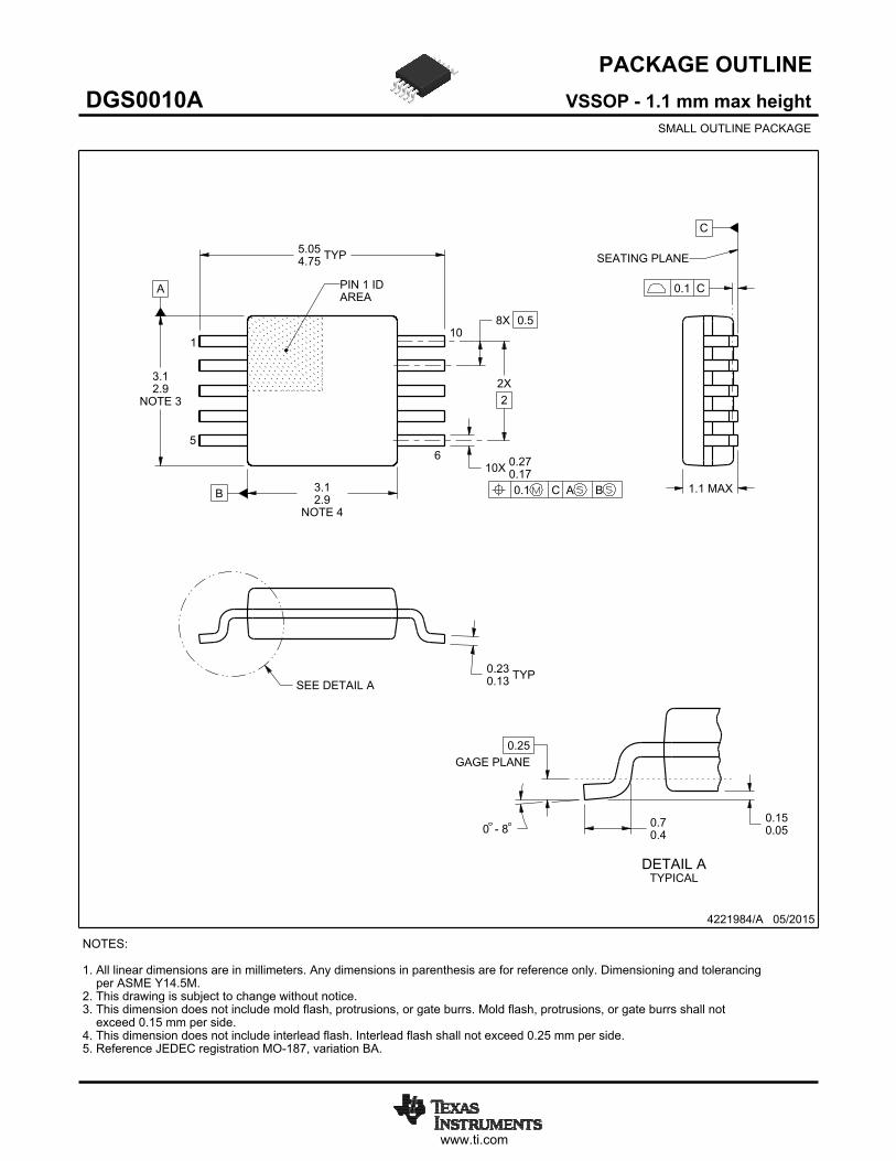
PACKAGE OUTLINE
C
TYP5.054.75
1.1 MAX
8X 0.5
10X 0.270.17
2X2
0.150.05
TYP0.230.13
0 - 8
0.25GAGE PLANE
0.70.4
A
NOTE 3
3.12.9
BNOTE 4
3.12.9
4221984/A 05/2015
VSSOP - 1.1 mm max heightDGS0010ASMALL OUTLINE PACKAGE
NOTES: 1. All linear dimensions are in millimeters. Any dimensions in parenthesis are for reference only. Dimensioning and tolerancing per ASME Y14.5M. 2. This drawing is subject to change without notice. 3. This dimension does not include mold flash, protrusions, or gate burrs. Mold flash, protrusions, or gate burrs shall not exceed 0.15 mm per side. 4. This dimension does not include interlead flash. Interlead flash shall not exceed 0.25 mm per side.5. Reference JEDEC registration MO-187, variation BA.
110
0.1 C A B
65
PIN 1 IDAREA
SEATING PLANE
0.1 C
SEE DETAIL A
DETAIL ATYPICAL
SCALE 3.200

www.ti.com
EXAMPLE BOARD LAYOUT
(4.4)
0.05 MAXALL AROUND
0.05 MINALL AROUND
10X (1.45)10X (0.3)
8X (0.5)
(R )TYP
0.05
4221984/A 05/2015
VSSOP - 1.1 mm max heightDGS0010ASMALL OUTLINE PACKAGE
SYMM
SYMM
LAND PATTERN EXAMPLESCALE:10X
1
5 6
10
NOTES: (continued) 6. Publication IPC-7351 may have alternate designs. 7. Solder mask tolerances between and around signal pads can vary based on board fabrication site.
METALSOLDER MASKOPENING
NON SOLDER MASKDEFINED
SOLDER MASK DETAILSNOT TO SCALE
SOLDER MASKOPENING
METAL UNDERSOLDER MASK
SOLDER MASKDEFINED

www.ti.com
EXAMPLE STENCIL DESIGN
(4.4)
8X (0.5)
10X (0.3)10X (1.45)
(R ) TYP0.05
4221984/A 05/2015
VSSOP - 1.1 mm max heightDGS0010ASMALL OUTLINE PACKAGE
NOTES: (continued) 8. Laser cutting apertures with trapezoidal walls and rounded corners may offer better paste release. IPC-7525 may have alternate design recommendations. 9. Board assembly site may have different recommendations for stencil design.
SYMM
SYMM
1
5 6
10
SOLDER PASTE EXAMPLEBASED ON 0.125 mm THICK STENCIL
SCALE:10X

IMPORTANT NOTICE AND DISCLAIMERTI PROVIDES TECHNICAL AND RELIABILITY DATA (INCLUDING DATASHEETS), DESIGN RESOURCES (INCLUDING REFERENCEDESIGNS), APPLICATION OR OTHER DESIGN ADVICE, WEB TOOLS, SAFETY INFORMATION, AND OTHER RESOURCES “AS IS”AND WITH ALL FAULTS, AND DISCLAIMS ALL WARRANTIES, EXPRESS AND IMPLIED, INCLUDING WITHOUT LIMITATION ANYIMPLIED WARRANTIES OF MERCHANTABILITY, FITNESS FOR A PARTICULAR PURPOSE OR NON-INFRINGEMENT OF THIRDPARTY INTELLECTUAL PROPERTY RIGHTS.These resources are intended for skilled developers designing with TI products. You are solely responsible for (1) selecting the appropriateTI products for your application, (2) designing, validating and testing your application, and (3) ensuring your application meets applicablestandards, and any other safety, security, or other requirements. These resources are subject to change without notice. TI grants youpermission to use these resources only for development of an application that uses the TI products described in the resource. Otherreproduction and display of these resources is prohibited. No license is granted to any other TI intellectual property right or to any third partyintellectual property right. TI disclaims responsibility for, and you will fully indemnify TI and its representatives against, any claims, damages,costs, losses, and liabilities arising out of your use of these resources.TI’s products are provided subject to TI’s Terms of Sale (https:www.ti.com/legal/termsofsale.html) or other applicable terms available eitheron ti.com or provided in conjunction with such TI products. TI’s provision of these resources does not expand or otherwise alter TI’sapplicable warranties or warranty disclaimers for TI products.IMPORTANT NOTICE
Mailing Address: Texas Instruments, Post Office Box 655303, Dallas, Texas 75265Copyright © 2021, Texas Instruments Incorporated