Embed Size (px)
Citation preview
PHYSICAL REVIEW B 87, 245401 (2013)
Transition between direct and indirect band gap in silicon nanocrystals
V. Kocevski, O. Eriksson, and J. RuszDepartment of Physics and Astronomy, Uppsala University, Box 516, SE-751 20 Uppsala, Sweden(Received 4 October 2012; revised manuscript received 20 February 2013; published 3 June 2013)
Using ground-state density functional theory we study the transition from indirect to direct band gap inhydrogen-terminated silicon nanocrystals (NCs) as a function of decreasing diameter. The studied range, from1.0 to 4.6 nm diameter of nanocrystals, with spherical and Wulff-shape NCs, covers the transition from nano- tobulk regime. A change in the symmetry of the lowest unoccupied state as a function of decreasing NC diameteris observed, gradually increasing the oscillator strength of transitions from the highest occupied to the lowestunoccupied state. Real space and Fourier space characteristics of highest occupied and lowest unoccupied statesare explored in detail and linked to a smooth transition from nano- to bulk regime.
DOI: 10.1103/PhysRevB.87.245401 PACS number(s): 73.22.−f, 42.70.Qs, 61.46.Df, 78.40.Fy
I. INTRODUCTION
Silicon is among the most important materials in optoelec-tronic devices, such as photodetectors and photovoltaic cells.However, the use of bulk silicon, as an active material in lightemitting devices, is limited because of its indirect nature ofthe electronic band gap. This disadvantage can be overcomeby structural manipulation at the nanoscale. The discoveryof photoluminescence from porous silicon1 confirmed that byconfining the lateral dimensions silicon can emit light. Sincethen, a great interest had been devoted to the study of siliconnanocrystals, and their fundamental physical properties.
The nanocrystals (NCs) exploit effects of quantumconfinement2,3—a change of the electronic structure of asystem, when some of its dimensions become comparable towavelengths of electrons in the sample. At these scales theband gap becomes wider and the absorption is blue-shifted, asthe size is reduced. This increase of the Si band gap shifts it tothe visible spectrum, and at the same time, the indirect natureof the gap undergoes a transformation. For an isolatednanocrystal there are no Bloch states and k vectors, since peri-odic boundary conditions are absent, therefore the notion of anindirect band gap has a different meaning. As already seen inprevious works4–7 and also detailed below, the HOMO-LUMOgap (also called Kohn-Sham gap in literature) and the onsetof optical absorption do in general occur at different energies,even in isolated NCs. This is the NC analog of the indirectband gap observed in bulk Si. Qualitatively, the widening ofthe gap can be understood as a narrowing of the bands, whenthe size of the system is reduced from bulk towards a singleatom. As a consequence, if the center of the band remainsapproximately at the same energy, the distance between theedges of occupied and unoccupied bands becomes larger.
Semiempirically, the NCs are often modeled as a Sicrystal with superimposed infinite spherical potential well8
employing the Luttinger model Hamiltonian9 and effec-tive mass approximation.10 More recently, a number ofinvestigations employed electronic structure calculations atvarious levels of sophistication, ranging from tight-bindingmethods,7,11,12 empirical pseudopotentials,13 via density func-tional theory4–6,14–16 (DFT), to the GW approximation com-bined with Bethe-Salpeter equation (BSE) or time-dependentDFT17–20 and diffusion Monte Carlo calculations (DMC).21
These methods have generally confirmed the quantum confine-ment on an ab initio level and provided valuable insight into theelectronic structure and optical properties, although, inevitablythe GW, BSE, and DMC methods were limited to rather smallSi clusters (<1.5 nm), so that details of the transition fromnano- to bulk regime were not accessible.
In this study we turn our attention to the transition fromthe indirect band gap, observed in the bulk, towards a directgap, seen in small NCs, and attempt to provide a microscopicexplanation by means of ground-state DFT calculations ofthe electronic structure and absorption spectra. Although weperform only ground-state DFT calculations, it was found thatthe cancellation of many-body effects and the excitonic effectsgive rise to DFT HOMO-LUMO gaps comparable with the ex-perimental optical gaps,5,12,21 although these effects go beyondthe main interest of our study. Previously, Trani et al.7 usedtight-binding methods to interpret this behavior of the bandgap in Si NCs in terms of increasing localization of the highestoccupied molecular orbital (HOMO) level in k space aroundthe � point, and localization of the lowest unoccupiedmolecular orbital (LUMO) level around the k point2πa
(0.83,0,0), as the diameter of the nanocrystal increases.Furthermore, Weissker et al.5 showed, using DFT-LDA,that with increasing size of the NCs, the tail in the energydependence of oscillator strength is becoming longer, whichhas been assigned to development of bulklike properties. Weextend these studies by a detailed investigation of HOMO andLUMO wave functions.
Structure of this manuscript is the following: In Sec. IIwe introduce our structural models for Si NCs—a sphericalmodel and two polyhedral structures with different planarterminations. We analyze the influence of NC shape onbasic characteristics, such as cohesive energy, valence bandwidth, and general shape of density of states. In Sec. III wediscuss in detail the HOMO-LUMO and optical absorptiongaps and their correlation with position-resolved electronicstructure (surface or interior of NCs). In Sec. IV we inspectthe spatial characteristics of highest occupied and lowestunoccupied eigenstates, HOMO and LUMO, both in real andreciprocal space. These provide an explicit picture of thegradual development of the bulk regime. Finally, concludingremarks are summarized in Sec. V.
245401-11098-0121/2013/87(24)/245401(9) ©2013 American Physical Society
V. KOCEVSKI, O. ERIKSSON, AND J. RUSZ PHYSICAL REVIEW B 87, 245401 (2013)
II. STRUCTURAL MODELS OF SILICON NANOCRYSTALS
We have analyzed the Si NCs of diameters 1.0 nm upto 4.6 nm using the pseudopotential DFT package SIESTA,22
which uses real space three-dimensional (3D) grid to appro-priate the real space integrals, charge densities and potentials,and numerical atomic orbitals allowing for very efficient yetreliable calculations. The fineness of the grid is governed by theplane-wave cutoff. We have used plane-wave cutoff of 160 Ry,which gives converged energies and DOS for bulk silicon.The basis size for Si atoms was single ζ with polarizationorbitals (SZP) and for hydrogen (H) double ζ . Since the maininterest of our study are the Si NCs, and their properties,thus we consider that H does not take an active part in thestudied properties. However, we have performed benchmarkcalculations for small Si clusters, using DZ and SZP for Hand SZP for Si, and we had seen that there is no significantdifference in the band gaps for a particular cluster, when DZ orSZP basis is used for H. In addition, the gain in computationalefficiency, by excluding polarization functions, is significant,especially for the bigger NCs. Furthermore, the results of theSIESTA calculations with SZP and DZ basis sets for Si and H,respectively, were cross-checked with the WIEN2K package,23
both in the bulk regime and for the smallest considered Si NCof diameter 1.0 nm. Good agreement was observed for statesup to ∼7.5 eV above the Fermi level.
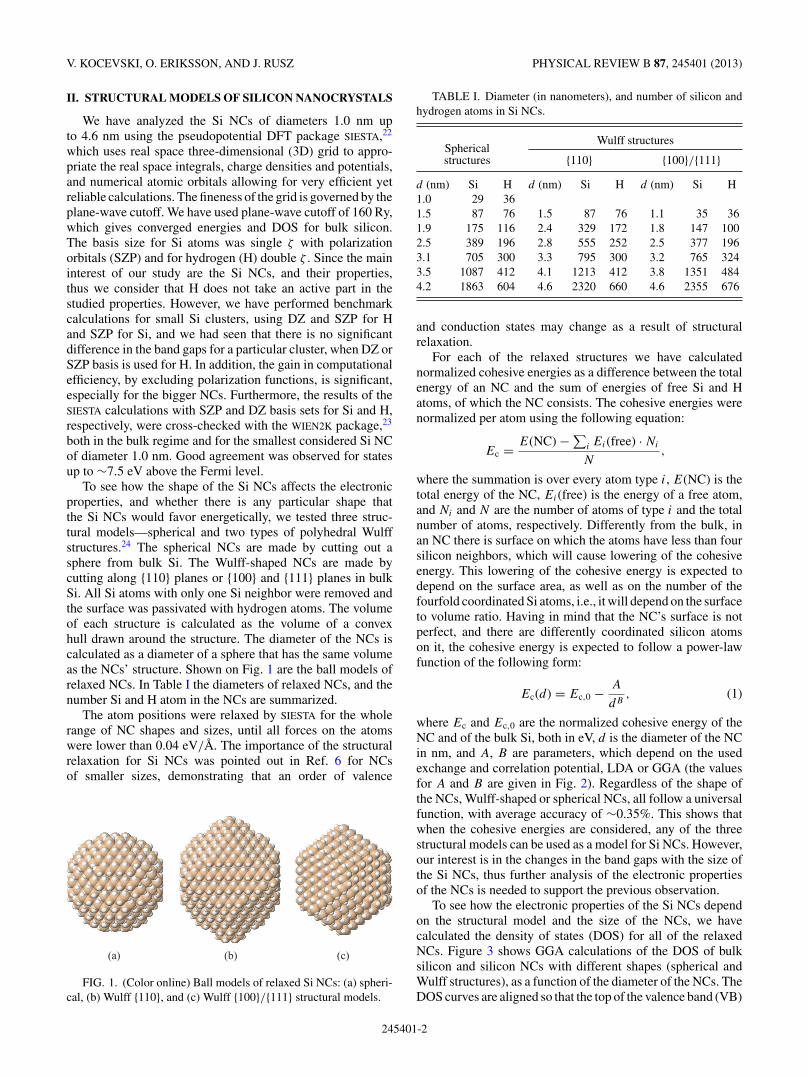
To see how the shape of the Si NCs affects the electronicproperties, and whether there is any particular shape thatthe Si NCs would favor energetically, we tested three struc-tural models—spherical and two types of polyhedral Wulffstructures.24 The spherical NCs are made by cutting out asphere from bulk Si. The Wulff-shaped NCs are made bycutting along {110} planes or {100} and {111} planes in bulkSi. All Si atoms with only one Si neighbor were removed andthe surface was passivated with hydrogen atoms. The volumeof each structure is calculated as the volume of a convexhull drawn around the structure. The diameter of the NCs iscalculated as a diameter of a sphere that has the same volumeas the NCs’ structure. Shown on Fig. 1 are the ball models ofrelaxed NCs. In Table I the diameters of relaxed NCs, and thenumber Si and H atom in the NCs are summarized.
The atom positions were relaxed by SIESTA for the wholerange of NC shapes and sizes, until all forces on the atomswere lower than 0.04 eV/A. The importance of the structuralrelaxation for Si NCs was pointed out in Ref. 6 for NCsof smaller sizes, demonstrating that an order of valence
(b) (c)(a)
FIG. 1. (Color online) Ball models of relaxed Si NCs: (a) spheri-cal, (b) Wulff {110}, and (c) Wulff {100}/{111} structural models.
TABLE I. Diameter (in nanometers), and number of silicon andhydrogen atoms in Si NCs.
SphericalWulff structures
structures {110} {100}/{111}d (nm) Si H d (nm) Si H d (nm) Si H1.0 29 361.5 87 76 1.5 87 76 1.1 35 361.9 175 116 2.4 329 172 1.8 147 1002.5 389 196 2.8 555 252 2.5 377 1963.1 705 300 3.3 795 300 3.2 765 3243.5 1087 412 4.1 1213 412 3.8 1351 4844.2 1863 604 4.6 2320 660 4.6 2355 676
and conduction states may change as a result of structuralrelaxation.
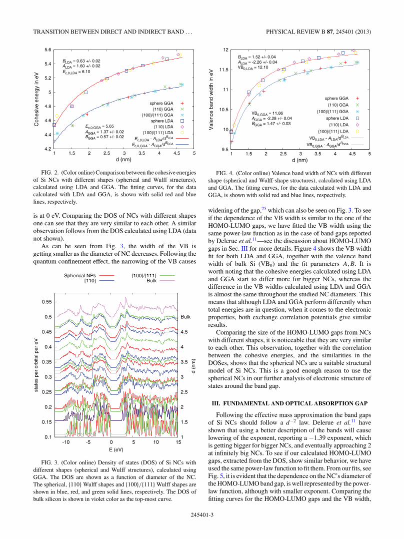
For each of the relaxed structures we have calculatednormalized cohesive energies as a difference between the totalenergy of an NC and the sum of energies of free Si and Hatoms, of which the NC consists. The cohesive energies werenormalized per atom using the following equation:
Ec = E(NC) − ∑i Ei(free) · Ni
N,
where the summation is over every atom type i, E(NC) is thetotal energy of the NC, Ei(free) is the energy of a free atom,and Ni and N are the number of atoms of type i and the totalnumber of atoms, respectively. Differently from the bulk, inan NC there is surface on which the atoms have less than foursilicon neighbors, which will cause lowering of the cohesiveenergy. This lowering of the cohesive energy is expected todepend on the surface area, as well as on the number of thefourfold coordinated Si atoms, i.e., it will depend on the surfaceto volume ratio. Having in mind that the NC’s surface is notperfect, and there are differently coordinated silicon atomson it, the cohesive energy is expected to follow a power-lawfunction of the following form:
Ec(d) = Ec,0 − A
dB, (1)
where Ec and Ec,0 are the normalized cohesive energy of theNC and of the bulk Si, both in eV, d is the diameter of the NCin nm, and A, B are parameters, which depend on the usedexchange and correlation potential, LDA or GGA (the valuesfor A and B are given in Fig. 2). Regardless of the shape ofthe NCs, Wulff-shaped or spherical NCs, all follow a universalfunction, with average accuracy of ∼0.35%. This shows thatwhen the cohesive energies are considered, any of the threestructural models can be used as a model for Si NCs. However,our interest is in the changes in the band gaps with the size ofthe Si NCs, thus further analysis of the electronic propertiesof the NCs is needed to support the previous observation.
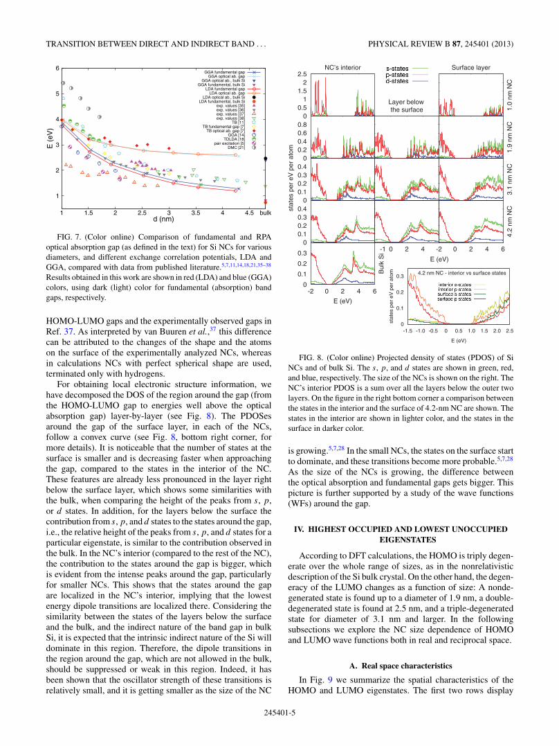
To see how the electronic properties of the Si NCs dependon the structural model and the size of the NCs, we havecalculated the density of states (DOS) for all of the relaxedNCs. Figure 3 shows GGA calculations of the DOS of bulksilicon and silicon NCs with different shapes (spherical andWulff structures), as a function of the diameter of the NCs. TheDOS curves are aligned so that the top of the valence band (VB)
245401-2
TRANSITION BETWEEN DIRECT AND INDIRECT BAND . . . PHYSICAL REVIEW B 87, 245401 (2013)
4.2
4.4
4.6
4.8
5
5.2
5.4
5.6
1 1.5 2 2.5 3 3.5 4 4.5 5
Coh
esiv
e en
ergy
in e
V
d (nm)
Ec,0,GGA = 5.65
BGGA = 0.57 +/- 0.02AGGA = 1.37 +/- 0.02
BLDA = 0.63 +/- 0.02ALDA = 1.60 +/- 0.02Ec,0,LDA = 6.10
sphere GGA{110} GGA
{100}/{111} GGAsphere LDA
{110} LDA{100}/{111} LDA
Ec,0,LDA - ALDA/dBLDA
Ec,0,GGA - AGGA/dBGGA
FIG. 2. (Color online) Comparison between the cohesive energiesof Si NCs with different shapes (spherical and Wulff structures),calculated using LDA and GGA. The fitting curves, for the datacalculated with LDA and GGA, is shown with solid red and bluelines, respectively.
is at 0 eV. Comparing the DOS of NCs with different shapesone can see that they are very similar to each other. A similarobservation follows from the DOS calculated using LDA (datanot shown).
As can be seen from Fig. 3, the width of the VB isgetting smaller as the diameter of NC decreases. Following thequantum confinement effect, the narrowing of the VB causes
0.1
0.15
0.2
0.25
0.3
0.35
0.4
0.45
0.5
0.55
-10 -5 0 5 10 151
1.5
2
2.5
3
3.5
4
4.5
Bulk
E (eV)
stat
es p
er o
rbita
l per
eV
d (n
m)
Spherical NPs{110}
{100}/{111}Bulk
FIG. 3. (Color online) Density of states (DOS) of Si NCs withdifferent shapes (spherical and Wulff structures), calculated usingGGA. The DOS are shown as a function of diameter of the NC.The spherical, {110} Wulff shapes and {100}/{111} Wulff shapes areshown in blue, red, and green solid lines, respectively. The DOS ofbulk silicon is shown in violet color as the top-most curve.
9.5
10
10.5
11
11.5
12
1 1.5 2 2.5 3 3.5 4 4.5 5
Val
ence
ban
d w
idth
in e
V
d (nm)
VB0,GGA = 11.86
BGGA = 1.47 +/- 0.03AGGA = -2.28 +/- 0.04
BLDA = 1.52 +/- 0.04ALDA = -2.26 +/- 0.04VB0,LDA = 12.10
sphere GGA
{110} GGA
{100}/{111} GGA
sphere LDA
{110} LDA
{100}/{111} LDA
VB0,LDA - ALDA/dBLDA
VB0,GGA - AGGA/dBGGA
FIG. 4. (Color online) Valence band width of NCs with differentshape (spherical and Wulff-shape structures), calculated using LDAand GGA. The fitting curves, for the data calculated with LDA andGGA, is shown with solid red and blue lines, respectively.
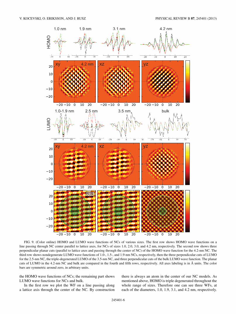
widening of the gap,25 which can also be seen on Fig. 3. To seeif the dependence of the VB width is similar to the one of theHOMO-LUMO gaps, we have fitted the VB width using thesame power-law function as in the case of band gaps reportedby Delerue et al.11—see the discussion about HOMO-LUMOgaps in Sec. III for more details. Figure 4 shows the VB widthfit for both LDA and GGA, together with the valence bandwidth of bulk Si (VB0) and the fit parameters A,B. It isworth noting that the cohesive energies calculated using LDAand GGA start to differ more for bigger NCs, whereas thedifference in the VB widths calculated using LDA and GGAis almost the same throughout the studied NC diameters. Thismeans that although LDA and GGA perform differently whentotal energies are in question, when it comes to the electronicproperties, both exchange correlation potentials give similarresults.
Comparing the size of the HOMO-LUMO gaps from NCswith different shapes, it is noticeable that they are very similarto each other. This observation, together with the correlationbetween the cohesive energies, and the similarities in theDOSes, shows that the spherical NCs are a suitable structuralmodel of Si NCs. This is a good enough reason to use thespherical NCs in our further analysis of electronic structure ofstates around the band gap.
III. FUNDAMENTAL AND OPTICAL ABSORPTION GAP
Following the effective mass approximation the band gapsof Si NCs should follow a d−2 law. Delerue et al.11 haveshown that using a better description of the bands will causelowering of the exponent, reporting a −1.39 exponent, whichis getting bigger for bigger NCs, and eventually approaching 2at infinitely big NCs. To see if our calculated HOMO-LUMOgaps, extracted from the DOS, show similar behavior, we haveused the same power-law function to fit them. From our fits, seeFig. 5, it is evident that the dependence on the NC’s diameter ofthe HOMO-LUMO band gap, is well represented by the power-law function, although with smaller exponent. Comparing thefitting curves for the HOMO-LUMO gaps and the VB width,
245401-3

V. KOCEVSKI, O. ERIKSSON, AND J. RUSZ PHYSICAL REVIEW B 87, 245401 (2013)
1
1.5
2
2.5
3
3.5
4
1 1.5 2 2.5 3 3.5 4 4.5
Eg
(eV
)
d (nm)
Eg,0,LDA = 0.83
BLDA = 1.20 +/- 0.05ALDA = 3.12 +/- 0.08
BGGA = 1.21 +/- 0.05AGGA = 3.16 +/- 0.08Eg,0,GGA = 0.74
LDA
GGA
Eg,0,LDA + ALDA/dBLDA
Eg,0,GGA + AGGA/dBGGA
FIG. 5. (Color online) Comparison of the fitted fundamental gaps(defined in the text), for Si NCs with various diameters, calculatedusing different exchange correlation potentials: LDA (red) and GGA(blue).
it is noticeable that the HOMO-LUMO gaps are changingmore rapidly with the diameter than the VB width, thanksto the larger magnitude of parameter A. This shows that theHOMO-LUMO gap does not depend solely on the VB width,but also on the changes in the conduction band width.
Here we should point out that in this work all thecalculations of gaps are based on the ground-state densityfunctional theory. Under the notion of fundamental gap weunderstand a difference between the energy of the lowestunoccupied eigenstate and the energy of the highest occupiedeigenstate in an NC, which is also called the Kohn-Sham gapin the literature.5 Calculating the optical absorption gap on thebase of ground-state DFT (also called an independent particlemodel) means that we employ a random-phase approximation(RPA) to the first-order time-dependent perturbation theory.26
For a detailed comparison to experiment one should includeeffects beyond the ground-state DFT, namely the many-bodyeffects and the excitonic effects.27 It is interesting to notethat more rigorous theoretical approaches have shown thatexcitonic and quasiparticle effects to a large extent cancel eachother, and as a consequence, the HOMO-LUMO gaps comparewell to measured optical gaps.5,12,21 Thus our comparison oftheoretical and experimental results should be understood inthis context. However, the main focus of our study is the directvs indirect nature of optical transitions in terms of ground-stateoscillator strengths, the nature of HOMO and LUMO states,and the evolution of these properties as a function of NCdiameter. In this sense, the excitonic and many-particle effectsgo beyond the scope of our study.
To extract the optical absorption gap, we have calculated theimaginary part of the dielectric tensor by explicitly evaluatingthe dipole transition matrix elements between all occupiedstates and unoccupied states up to 15 eV above the top ofthe valence band. Using the Kramers-Kronig transformation,the real part of the dielectric tensor was obtained, andhence the refraction and absorption indices—the latter isshown in Fig. 6. Our absorption spectra qualitatively agree withcalculations of Ref. 13, although for smaller clusters our DFTcalculations predict a broader spectrum than that of Ref. 13.
FIG. 6. (Color online) Absorption index (right axes) of Si NCs asa function of the diameter (left axes) and energy, and the exchangecorrelation potential: (i) LDA (red); (ii) GGA (dotted line). For bulkSi it is shown on the top (the k values for the bulk are scaled by 2).The khaki and pink colored areas depict the HOMO-LUMO gap andthe optical absorption gap, respectively.
The shapes of calculated absorption spectra agree well withprevious measurements.29,30 A recent experimental work for4-nm Si NCs31 also matches well with our calculations. Fromthe absorption indices we extracted the optical absorptiongap—an energy at which the absorption index becomes largerthan a given threshold. Although, small nonzero contributionsto the absorption index appear below this optical absorptionthreshold, these matrix elements are typically of negligiblesizes. As a practical solution for the optical absorptionthreshold, we have chosen a value of 0.1, which is two orders ofmagnitude smaller than the maximum of the absorption peak.Different threshold criteria have been used in literature (see,e.g., Ref. 7), all leading to very similar quantitative results.
A comparison of the fundamental gap and the opticalabsorption gap, extracted with the above-mentioned criterion,is shown in Fig. 7. As the size of the NC increases, thedifference between the optical absorption and fundamental gapalso increases, approaching the difference between the bulk� − � gap and the bulk � − X gap. Following the conceptionthat bulk Si has an indirect gap, implying a difference betweenthe optical absorption and fundamental gap, the coalescingof these two gaps at the smallest sizes, around 1.0 nm,allows us to speak about Si in this size range as a direct gapmaterial. This finding was previously obtained by tight-bindingmodel calculations7 and was also confirmed by our WIEN2K
calculations. For the largest considered NC both gaps areclose to the bulk values. However, the fundamental and theoptical absorption gaps of the bulk material are somewhatlower, suggesting an importance of the surface effects in allof the NC structures investigated here. Similar behavior ofthe fundamental and the optical absorption gaps has beenobserved in Si nanowires32,33 and nanotubes.34 There is agood qualitative agreement, in terms of trend, between thetheoretical HOMO-LUMO gap and experimental data,35–38 asis clear from Fig. 7. This is in accord with above-mentionedcancellation of the quasiparticle and excitonic effects. How-ever, there is noticeable difference between our calculated
245401-4
TRANSITION BETWEEN DIRECT AND INDIRECT BAND . . . PHYSICAL REVIEW B 87, 245401 (2013)
1
2
3
4
5
6
1 1.5 2 2.5 3 3.5 4 4.5 bulk
E (
eV)
d (nm)
GGA fundamental gapGGA optical ab. gap
GGA optical ab., bulk SiGGA fundamental, bulk Si
LDA fundamental gapLDA optical ab. gap
LDA optical ab., bulk SiLDA fundamental, bulk Si
exp. values [35]exp. values [36]exp. values [37]exp. values [38]
TB [11]TB fundamental gap [7]
TB optical ab. gap [7]GGA [14]
TDLDA [18]pair excitation [5]
DMC [21]
FIG. 7. (Color online) Comparison of fundamental and RPAoptical absorption gap (as defined in the text) for Si NCs for variousdiameters, and different exchange correlation potentials, LDA andGGA, compared with data from published literature.5,7,11,14,18,21,35–38
Results obtained in this work are shown in red (LDA) and blue (GGA)colors, using dark (light) color for fundamental (absorption) bandgaps, respectively.
HOMO-LUMO gaps and the experimentally observed gaps inRef. 37. As interpreted by van Buuren et al.,37 this differencecan be attributed to the changes of the shape and the atomson the surface of the experimentally analyzed NCs, whereasin calculations NCs with perfect spherical shape are used,terminated only with hydrogens.
For obtaining local electronic structure information, wehave decomposed the DOS of the region around the gap (fromthe HOMO-LUMO gap to energies well above the opticalabsorption gap) layer-by-layer (see Fig. 8). The PDOSesaround the gap of the surface layer, in each of the NCs,follow a convex curve (see Fig. 8, bottom right corner, formore details). It is noticeable that the number of states at thesurface is smaller and is decreasing faster when approachingthe gap, compared to the states in the interior of the NC.These features are already less pronounced in the layer rightbelow the surface layer, which shows some similarities withthe bulk, when comparing the height of the peaks from s, p,or d states. In addition, for the layers below the surface thecontribution from s, p, and d states to the states around the gap,i.e., the relative height of the peaks from s, p, and d states for aparticular eigenstate, is similar to the contribution observed inthe bulk. In the NC’s interior (compared to the rest of the NC),the contribution to the states around the gap is bigger, whichis evident from the intense peaks around the gap, particularlyfor smaller NCs. This shows that the states around the gapare localized in the NC’s interior, implying that the lowestenergy dipole transitions are localized there. Considering thesimilarity between the states of the layers below the surfaceand the bulk, and the indirect nature of the band gap in bulkSi, it is expected that the intrinsic indirect nature of the Si willdominate in this region. Therefore, the dipole transitions inthe region around the gap, which are not allowed in the bulk,should be suppressed or weak in this region. Indeed, it hasbeen shown that the oscillator strength of these transitions isrelatively small, and it is getting smaller as the size of the NC
0
0.1
0.2
0.3
-2 0 2 4 6
Bul
kS
i
E (eV)
00.10.20.30.4
-1 0 2 4
E (eV)
-2 0 2 4 6
4.2
nmN
C
00.10.20.30.4
stat
espe
reV
per
atom
3.1
nmN
C
00.20.40.60.8
the surfaceLayer below
1.9
nmN
C
00.5
11.5
22.5
NC’s interior
1.0
nmN
C
Surface layer
0
0.1
0.2
0.3
-1.5 -1.0 -0.5 0 0.5 1.0 1.5 2.0 2.5
E (eV)
4.2 nm NC - interior vs surface states
stat
espe
reV
per
atom
FIG. 8. (Color online) Projected density of states (PDOS) of SiNCs and of bulk Si. The s, p, and d states are shown in green, red,and blue, respectively. The size of the NCs is shown on the right. TheNC’s interior PDOS is a sum over all the layers below the outer twolayers. On the figure in the right bottom corner a comparison betweenthe states in the interior and the surface of 4.2-nm NC are shown. Thestates in the interior are shown in lighter color, and the states in thesurface in darker color.
is growing.5,7,28 In the small NCs, the states on the surface startto dominate, and these transitions become more probable.5,7,28
As the size of the NCs is growing, the difference betweenthe optical absorption and fundamental gaps gets bigger. Thispicture is further supported by a study of the wave functions(WFs) around the gap.
IV. HIGHEST OCCUPIED AND LOWEST UNOCCUPIEDEIGENSTATES
According to DFT calculations, the HOMO is triply degen-erate over the whole range of sizes, as in the nonrelativisticdescription of the Si bulk crystal. On the other hand, the degen-eracy of the LUMO changes as a function of size: A nonde-generated state is found up to a diameter of 1.9 nm, a double-degenerated state is found at 2.5 nm, and a triple-degeneratedstate for diameter of 3.1 nm and larger. In the followingsubsections we explore the NC size dependence of HOMOand LUMO wave functions both in real and reciprocal space.
A. Real space characteristics
In Fig. 9 we summarize the spatial characteristics of theHOMO and LUMO eigenstates. The first two rows display
245401-5
V. KOCEVSKI, O. ERIKSSON, AND J. RUSZ PHYSICAL REVIEW B 87, 245401 (2013)
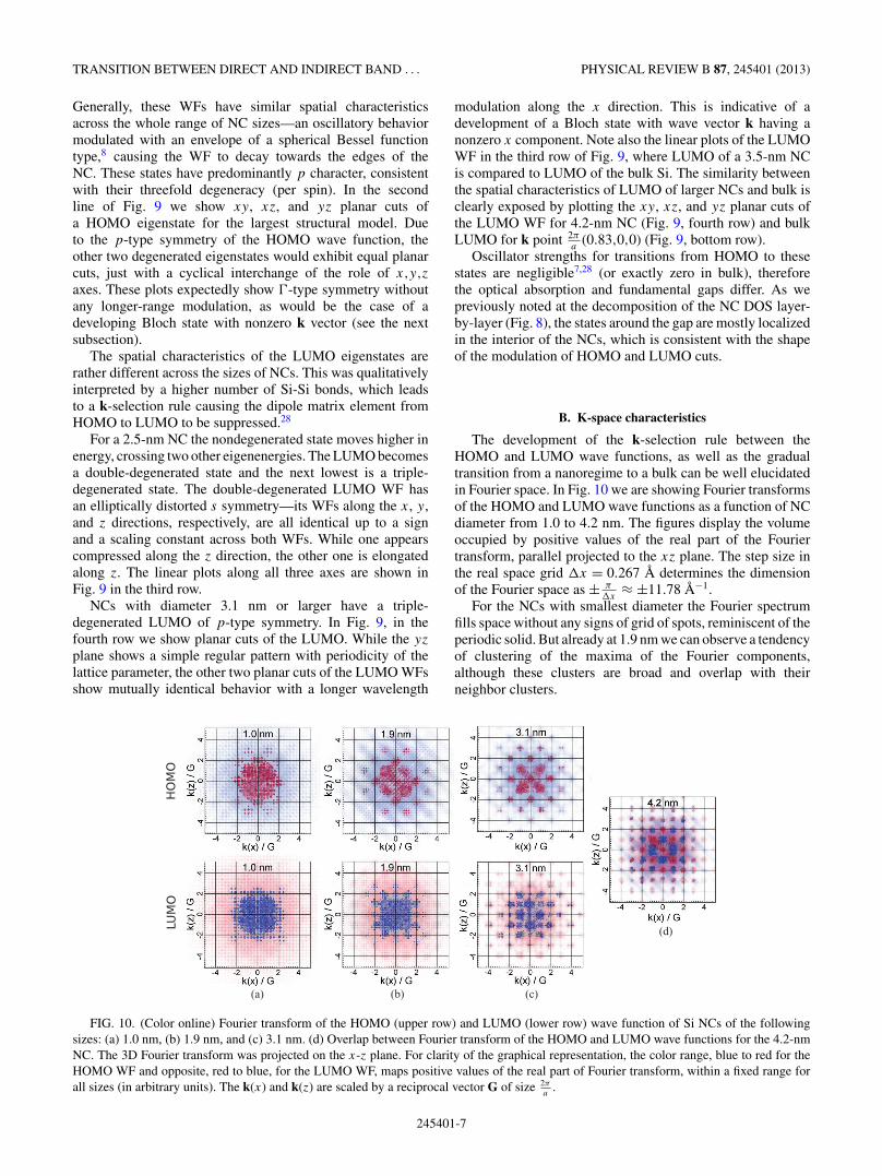
FIG. 9. (Color online) HOMO and LUMO wave functions of NCs of various sizes. The first row shows HOMO wave functions on aline passing through NC center parallel to lattice axes, for NCs of sizes 1.0, 2.0, 3.0, and 4.2 nm, respectively. The second row shows threeperpendicular planar cuts (parallel to lattice axes and passing through the center of NC) of the HOMO wave function for the 4.2-nm NC. Thethird row shows nondegenerate LUMO wave functions of 1.0-, 1.5-, and 1.9-nm NCs, respectively, then the three perpendicular cuts of LUMOfor the 2.5-nm NC, the triple-degenerated LUMO of the 3.5-nm NC, and three perpendicular cuts of the bulk LUMO wave function. The planarcuts of LUMO in the 4.2-nm NC and bulk are compared in the fourth and fifth rows, respectively. All axes labeling is in A units. The colorbars are symmetric around zero, in arbitrary units.
the HOMO wave functions of NCs; the remaining part showsLUMO wave functions for NCs and bulk.
In the first row we plot the WF on a line passing alonga lattice axis through the center of the NC. By construction
there is always an atom in the center of our NC models. Asmentioned above, HOMO is triple degenerated throughout thewhole range of sizes. Therefore one can see three WFs, ateach of the diameters, 1.0, 1.9, 3.1, and 4.2 nm, respectively.
245401-6
TRANSITION BETWEEN DIRECT AND INDIRECT BAND . . . PHYSICAL REVIEW B 87, 245401 (2013)
Generally, these WFs have similar spatial characteristicsacross the whole range of NC sizes—an oscillatory behaviormodulated with an envelope of a spherical Bessel functiontype,8 causing the WF to decay towards the edges of theNC. These states have predominantly p character, consistentwith their threefold degeneracy (per spin). In the secondline of Fig. 9 we show xy, xz, and yz planar cuts ofa HOMO eigenstate for the largest structural model. Dueto the p-type symmetry of the HOMO wave function, theother two degenerated eigenstates would exhibit equal planarcuts, just with a cyclical interchange of the role of x,y,z
axes. These plots expectedly show �-type symmetry withoutany longer-range modulation, as would be the case of adeveloping Bloch state with nonzero k vector (see the nextsubsection).
The spatial characteristics of the LUMO eigenstates arerather different across the sizes of NCs. This was qualitativelyinterpreted by a higher number of Si-Si bonds, which leadsto a k-selection rule causing the dipole matrix element fromHOMO to LUMO to be suppressed.28
For a 2.5-nm NC the nondegenerated state moves higher inenergy, crossing two other eigenenergies. The LUMO becomesa double-degenerated state and the next lowest is a triple-degenerated state. The double-degenerated LUMO WF hasan elliptically distorted s symmetry—its WFs along the x, y,and z directions, respectively, are all identical up to a signand a scaling constant across both WFs. While one appearscompressed along the z direction, the other one is elongatedalong z. The linear plots along all three axes are shown inFig. 9 in the third row.
NCs with diameter 3.1 nm or larger have a triple-degenerated LUMO of p-type symmetry. In Fig. 9, in thefourth row we show planar cuts of the LUMO. While the yz
plane shows a simple regular pattern with periodicity of thelattice parameter, the other two planar cuts of the LUMO WFsshow mutually identical behavior with a longer wavelength
modulation along the x direction. This is indicative of adevelopment of a Bloch state with wave vector k having anonzero x component. Note also the linear plots of the LUMOWF in the third row of Fig. 9, where LUMO of a 3.5-nm NCis compared to LUMO of the bulk Si. The similarity betweenthe spatial characteristics of LUMO of larger NCs and bulk isclearly exposed by plotting the xy, xz, and yz planar cuts ofthe LUMO WF for 4.2-nm NC (Fig. 9, fourth row) and bulkLUMO for k point 2π
a(0.83,0,0) (Fig. 9, bottom row).
Oscillator strengths for transitions from HOMO to thesestates are negligible7,28 (or exactly zero in bulk), thereforethe optical absorption and fundamental gaps differ. As wepreviously noted at the decomposition of the NC DOS layer-by-layer (Fig. 8), the states around the gap are mostly localizedin the interior of the NCs, which is consistent with the shapeof the modulation of HOMO and LUMO cuts.
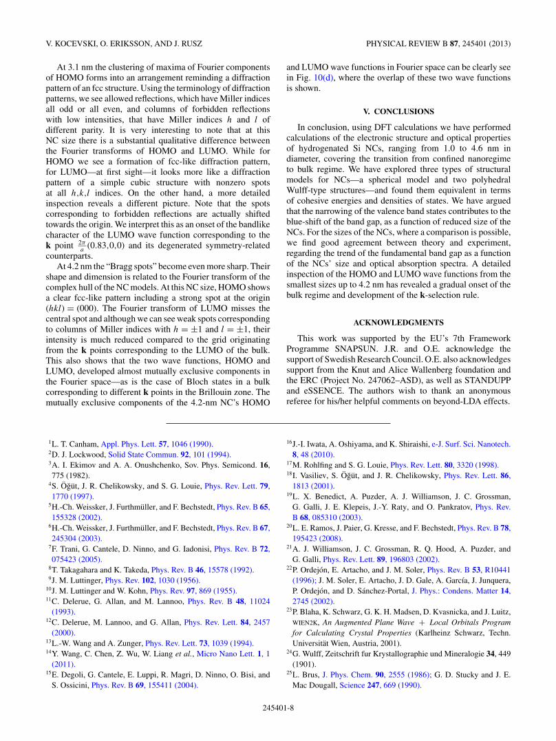
B. K-space characteristics
The development of the k-selection rule between theHOMO and LUMO wave functions, as well as the gradualtransition from a nanoregime to a bulk can be well elucidatedin Fourier space. In Fig. 10 we are showing Fourier transformsof the HOMO and LUMO wave functions as a function of NCdiameter from 1.0 to 4.2 nm. The figures display the volumeoccupied by positive values of the real part of the Fouriertransform, parallel projected to the xz plane. The step size inthe real space grid �x = 0.267 A determines the dimensionof the Fourier space as ± π
�x≈ ±11.78 A−1.
For the NCs with smallest diameter the Fourier spectrumfills space without any signs of grid of spots, reminiscent of theperiodic solid. But already at 1.9 nm we can observe a tendencyof clustering of the maxima of the Fourier components,although these clusters are broad and overlap with theirneighbor clusters.
(a) (b) (c)
(d)
FIG. 10. (Color online) Fourier transform of the HOMO (upper row) and LUMO (lower row) wave function of Si NCs of the followingsizes: (a) 1.0 nm, (b) 1.9 nm, and (c) 3.1 nm. (d) Overlap between Fourier transform of the HOMO and LUMO wave functions for the 4.2-nmNC. The 3D Fourier transform was projected on the x-z plane. For clarity of the graphical representation, the color range, blue to red for theHOMO WF and opposite, red to blue, for the LUMO WF, maps positive values of the real part of Fourier transform, within a fixed range forall sizes (in arbitrary units). The k(x) and k(z) are scaled by a reciprocal vector G of size 2π
a.
245401-7
V. KOCEVSKI, O. ERIKSSON, AND J. RUSZ PHYSICAL REVIEW B 87, 245401 (2013)
At 3.1 nm the clustering of maxima of Fourier componentsof HOMO forms into an arrangement reminding a diffractionpattern of an fcc structure. Using the terminology of diffractionpatterns, we see allowed reflections, which have Miller indicesall odd or all even, and columns of forbidden reflectionswith low intensities, that have Miller indices h and l ofdifferent parity. It is very interesting to note that at thisNC size there is a substantial qualitative difference betweenthe Fourier transforms of HOMO and LUMO. While forHOMO we see a formation of fcc-like diffraction pattern,for LUMO—at first sight—it looks more like a diffractionpattern of a simple cubic structure with nonzero spotsat all h,k,l indices. On the other hand, a more detailedinspection reveals a different picture. Note that the spotscorresponding to forbidden reflections are actually shiftedtowards the origin. We interpret this as an onset of the bandlikecharacter of the LUMO wave function corresponding to thek point 2π
a(0.83,0,0) and its degenerated symmetry-related
counterparts.At 4.2 nm the “Bragg spots” become even more sharp. Their
shape and dimension is related to the Fourier transform of thecomplex hull of the NC models. At this NC size, HOMO showsa clear fcc-like pattern including a strong spot at the origin(hkl) = (000). The Fourier transform of LUMO misses thecentral spot and although we can see weak spots correspondingto columns of Miller indices with h = ±1 and l = ±1, theirintensity is much reduced compared to the grid originatingfrom the k points corresponding to the LUMO of the bulk.This also shows that the two wave functions, HOMO andLUMO, developed almost mutually exclusive components inthe Fourier space—as is the case of Bloch states in a bulkcorresponding to different k points in the Brillouin zone. Themutually exclusive components of the 4.2-nm NC’s HOMO
and LUMO wave functions in Fourier space can be clearly seein Fig. 10(d), where the overlap of these two wave functionsis shown.
V. CONCLUSIONS
In conclusion, using DFT calculations we have performedcalculations of the electronic structure and optical propertiesof hydrogenated Si NCs, ranging from 1.0 to 4.6 nm indiameter, covering the transition from confined nanoregimeto bulk regime. We have explored three types of structuralmodels for NCs—a spherical model and two polyhedralWulff-type structures—and found them equivalent in termsof cohesive energies and densities of states. We have arguedthat the narrowing of the valence band states contributes to theblue-shift of the band gap, as a function of reduced size of theNCs. For the sizes of the NCs, where a comparison is possible,we find good agreement between theory and experiment,regarding the trend of the fundamental band gap as a functionof the NCs’ size and optical absorption spectra. A detailedinspection of the HOMO and LUMO wave functions from thesmallest sizes up to 4.2 nm has revealed a gradual onset of thebulk regime and development of the k-selection rule.
ACKNOWLEDGMENTS
This work was supported by the EU’s 7th FrameworkProgramme SNAPSUN. J.R. and O.E. acknowledge thesupport of Swedish Research Council. O.E. also acknowledgessupport from the Knut and Alice Wallenberg foundation andthe ERC (Project No. 247062–ASD), as well as STANDUPPand eSSENCE. The authors wish to thank an anonymousreferee for his/her helpful comments on beyond-LDA effects.
1L. T. Canham, Appl. Phys. Lett. 57, 1046 (1990).2D. J. Lockwood, Solid State Commun. 92, 101 (1994).3A. I. Ekimov and A. A. Onushchenko, Sov. Phys. Semicond. 16,775 (1982).
4S. Ogut, J. R. Chelikowsky, and S. G. Louie, Phys. Rev. Lett. 79,1770 (1997).
5H.-Ch. Weissker, J. Furthmuller, and F. Bechstedt, Phys. Rev. B 65,155328 (2002).
6H.-Ch. Weissker, J. Furthmuller, and F. Bechstedt, Phys. Rev. B 67,245304 (2003).
7F. Trani, G. Cantele, D. Ninno, and G. Iadonisi, Phys. Rev. B 72,075423 (2005).
8T. Takagahara and K. Takeda, Phys. Rev. B 46, 15578 (1992).9J. M. Luttinger, Phys. Rev. 102, 1030 (1956).
10J. M. Luttinger and W. Kohn, Phys. Rev. 97, 869 (1955).11C. Delerue, G. Allan, and M. Lannoo, Phys. Rev. B 48, 11024
(1993).12C. Delerue, M. Lannoo, and G. Allan, Phys. Rev. Lett. 84, 2457
(2000).13L.-W. Wang and A. Zunger, Phys. Rev. Lett. 73, 1039 (1994).14Y. Wang, C. Chen, Z. Wu, W. Liang et al., Micro Nano Lett. 1, 1
(2011).15E. Degoli, G. Cantele, E. Luppi, R. Magri, D. Ninno, O. Bisi, and
S. Ossicini, Phys. Rev. B 69, 155411 (2004).
16J.-I. Iwata, A. Oshiyama, and K. Shiraishi, e-J. Surf. Sci. Nanotech.8, 48 (2010).
17M. Rohlfing and S. G. Louie, Phys. Rev. Lett. 80, 3320 (1998).18I. Vasiliev, S. Ogut, and J. R. Chelikowsky, Phys. Rev. Lett. 86,
1813 (2001).19L. X. Benedict, A. Puzder, A. J. Williamson, J. C. Grossman,
G. Galli, J. E. Klepeis, J.-Y. Raty, and O. Pankratov, Phys. Rev.B 68, 085310 (2003).
20L. E. Ramos, J. Paier, G. Kresse, and F. Bechstedt, Phys. Rev. B 78,195423 (2008).
21A. J. Williamson, J. C. Grossman, R. Q. Hood, A. Puzder, andG. Galli, Phys. Rev. Lett. 89, 196803 (2002).
22P. Ordejon, E. Artacho, and J. M. Soler, Phys. Rev. B 53, R10441(1996); J. M. Soler, E. Artacho, J. D. Gale, A. Garcıa, J. Junquera,P. Ordejon, and D. Sanchez-Portal, J. Phys.: Condens. Matter 14,2745 (2002).
23P. Blaha, K. Schwarz, G. K. H. Madsen, D. Kvasnicka, and J. Luitz,WIEN2K, An Augmented Plane Wave + Local Orbitals Programfor Calculating Crystal Properties (Karlheinz Schwarz, Techn.Universitat Wien, Austria, 2001).
24G. Wulff, Zeitschrift fur Krystallographie und Mineralogie 34, 449(1901).
25L. Brus, J. Phys. Chem. 90, 2555 (1986); G. D. Stucky and J. E.Mac Dougall, Science 247, 669 (1990).
245401-8
TRANSITION BETWEEN DIRECT AND INDIRECT BAND . . . PHYSICAL REVIEW B 87, 245401 (2013)
26S. L. Adler, Phys. Rev. 126, 413 (1962).27G. Onida, L. Reining, and A. Rubio, Rev. Mod. Phys. 74, 601
(2002).28B. Delley and E. F. Steigmeier, Phys. Rev. B 47, 1397 (1993).29N. Koshida, H. Koyama, Y. Suda, Y. Yamamoto, M. Araki, T. Saito,
K. Sato, N. Sata, and S. Shin, Appl. Phys. Lett. 63, 2774 (1993).30D. Amans, S. Callard, A. Gagnaire, J. Joseph, G. Ledoux, and
F. Huisken, J. Appl. Phys. 93, 4173 (2003).31M. Mansour, A. En Naciri, L. Johann, J. J. Grob, and
M. Stchakovsky, Phys. Status Solidi A 205, 845 (2008).32X. Zhao, C. M. Wei, L. Yang, and M. Y. Chou, Phys. Rev. Lett. 92,
236805 (2004).
33T. Vo, A. J. Williamson, and G. Galli, Phys. Rev. B 74, 045116(2006).
34M. Ni, G. F. Luo, J. Lu et al., Nanotechnology 18, 505707(2007).
35S. Furukawa and T. Miyasato, Phys. Rev. B 38, 5726(1988).
36M. V. Wolkin, J. Jorne, P. M. Fauchet, G. Allan, and C. Delerue,Phys. Rev. Lett. 82, 197 (1999).
37T. van Buuren, L. N. Dinh, L. L. Chase, W. J. Siekhaus, and L. J.Terminello, Phys. Rev. Lett. 80, 3803 (1998).
38G. Ledoux, O. Guillois, D. Porterat, C. Reynaud, F. Huisken,B. Kohn, and V. Paillard, Phys. Rev. B 62, 15942 (2000).
245401-9


![Indirect Speech - · PDF fileSusan to Klaus: „I like you!“ ... Lisa didn’t leave. k) ... [INDIRECT SPEECH] Indirect Speech](https://img.pdfslide.us/doc/110x75/5a791c9e7f8b9a9d218df6f7/indirect-speech-to-klaus-i-like-you-lisa-didnt-leave-k-indirect.jpg)