Embed Size (px)
Citation preview
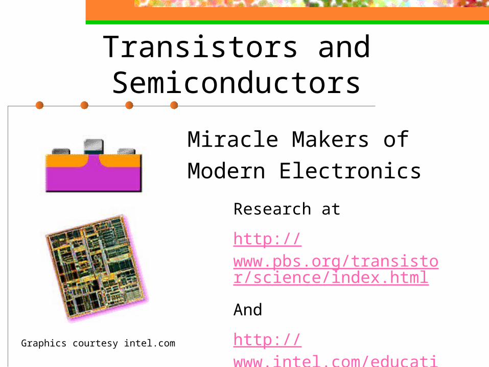
Transistors and Semiconductors
Miracle Makers of Modern Electronics
Graphics courtesy intel.com
Research at
http://www.pbs.org/transistor/science/index.html
And
http://www.intel.com/education/transworks/index.htm?iid=search&
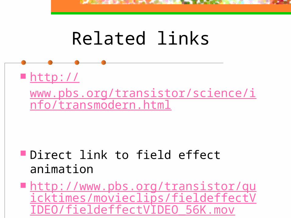
Related links
http://www.pbs.org/transistor/science/info/transmodern.html
Direct link to field effect animation http://www.pbs.org/transistor/quick
times/movieclips/fieldeffectVIDEO/fieldeffectVIDEO_56K.mov
State Standard
Student know the properties of transistors and the role of transistors in electric circuits.
Microchip vs Transistor vs. Semiconductor
Semiconductor- element with both conducting and insulating properties
Transistor – an electronic device that uses properties of semiconductors
Microchip – contains many transistors

Before Transistors
There was the vacuum tube
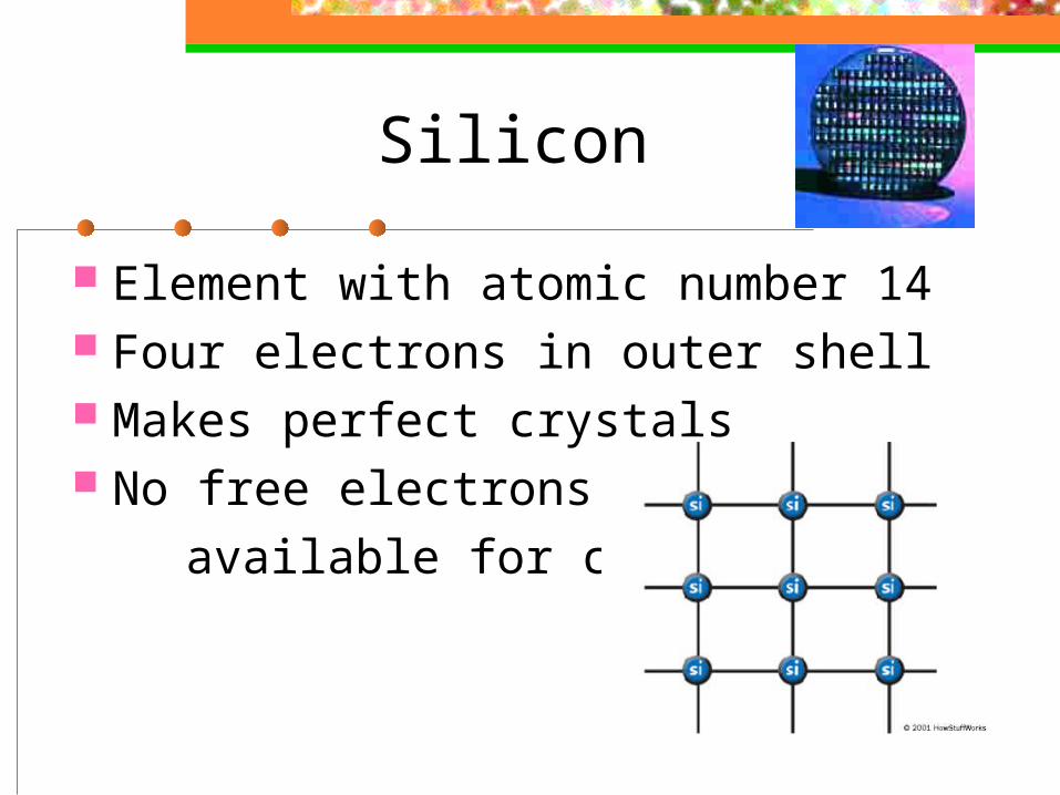
Silicon
Element with atomic number 14 Four electrons in outer shell Makes perfect crystals No free electrons available for conduction
Doping – Add Impurities
Add phosphorus or arsenic with 5 outer electrons – provides free electrons needed for electric current to flow
Makes N- type silicon Charges that flow are negative –
electrons Doped silicon is “semiconductor”
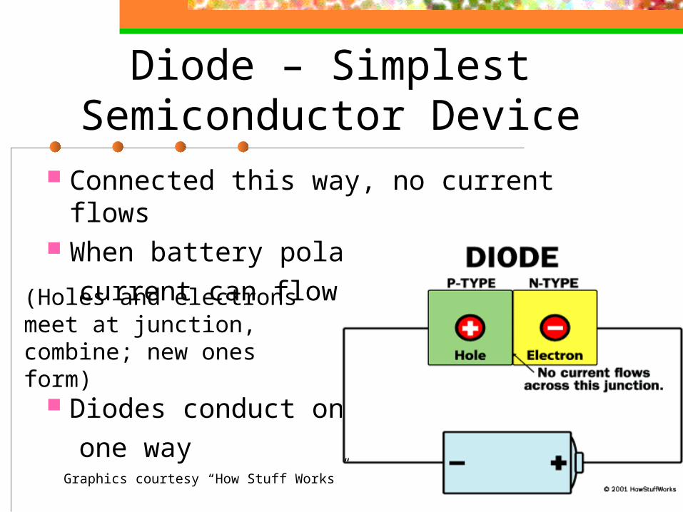
Diode – Simplest Semiconductor Device
Connected this way, no current flows When battery polarity reversed current can flow
Diodes conduct only one way
Graphics courtesy “How Stuff Works”
(Holes and electrons meet at junction, combine; new ones form)
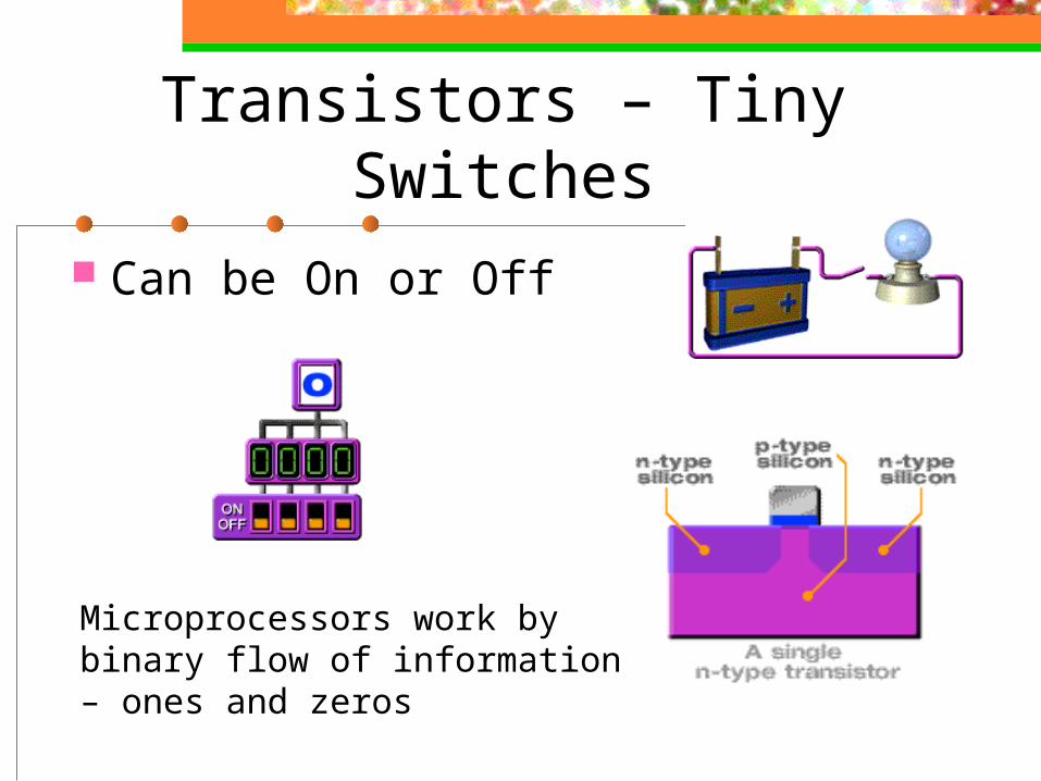
Transistors – Tiny Switches
Can be On or Off
Microprocessors work by binary flow of information – ones and zeros
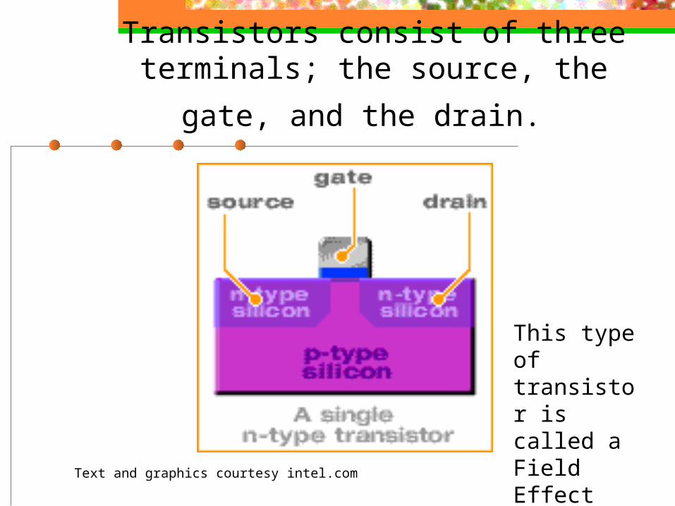
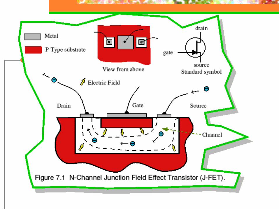
Transistors consist of three terminals;
the source, the gate, and the drain.
Text and graphics courtesy intel.com
This type of transistor is called a Field Effect Transistor
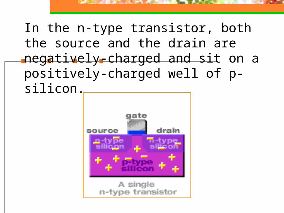
In the n-type transistor, both the source and the drain are negatively-charged and sit on a positively-charged well of p-silicon.

When positive voltage is applied to the gate, electrons in the p-silicon are attracted to the area under the gate forming an electron channel between the source and the drain.
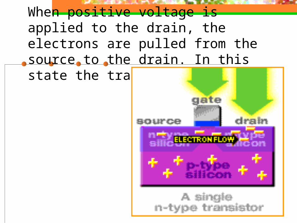
When positive voltage is applied to the drain, the electrons are pulled from the source to the drain. In this state the transistor is on.
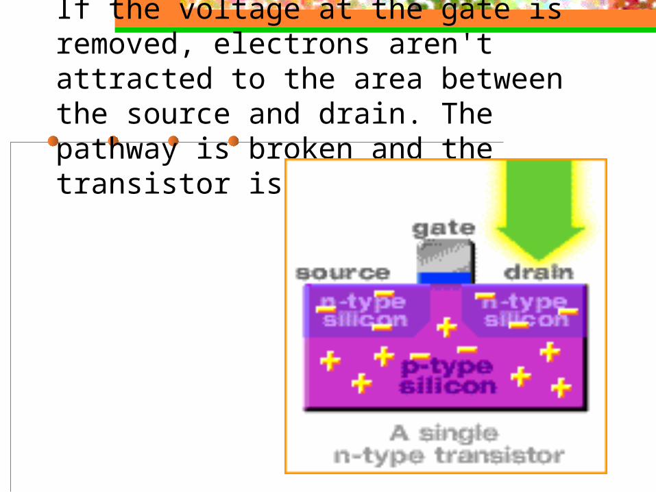
If the voltage at the gate is removed, electrons aren't attracted to the area between the source and drain. The pathway is broken and the transistor is turned off.
P – Type Transistors
Add boron or gallium to silicon Have only three outer electrons Form “holes” that can accept an
electron from a neighbor Also conducts current Majority current carriers are holes
(+) rather than electrons (-) Less common today
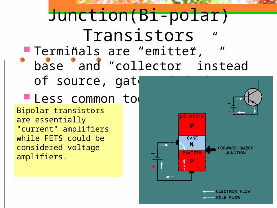
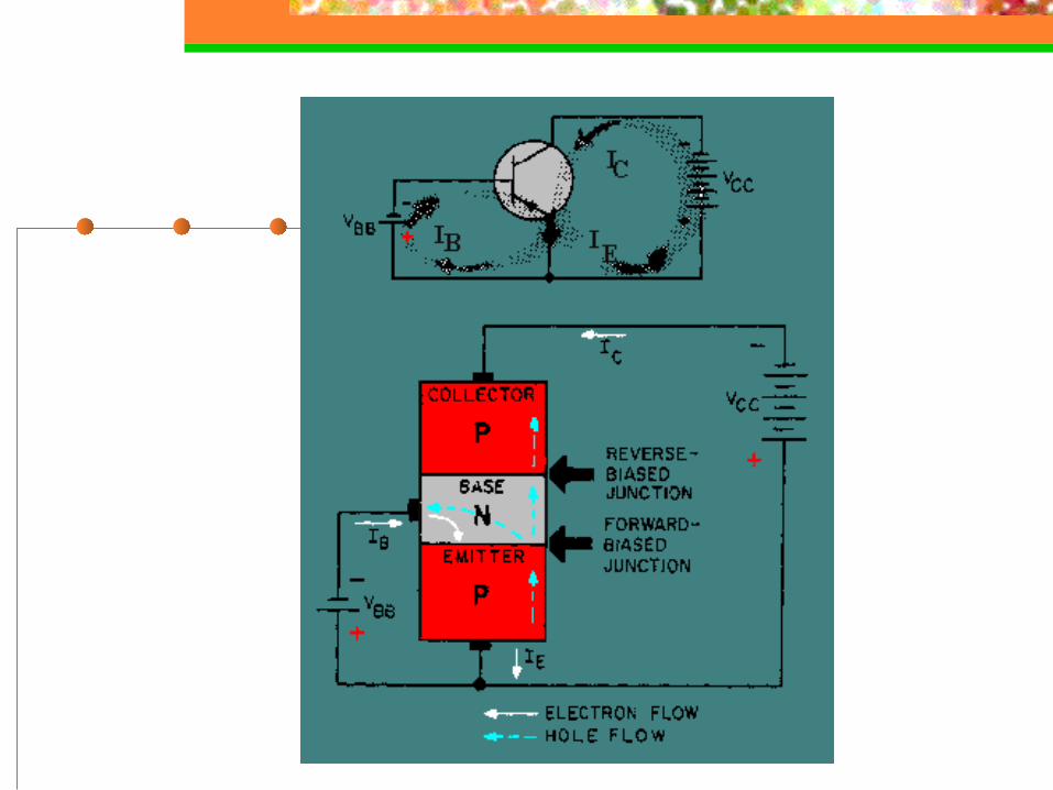
Junction(Bi-polar) Transistors
Terminals are “emitter,” “ base” and “collector” instead of source, gate and drain
Less common todayBipolar transistors are essentially "current" amplifiers while FETS could be considered voltage amplifiers.
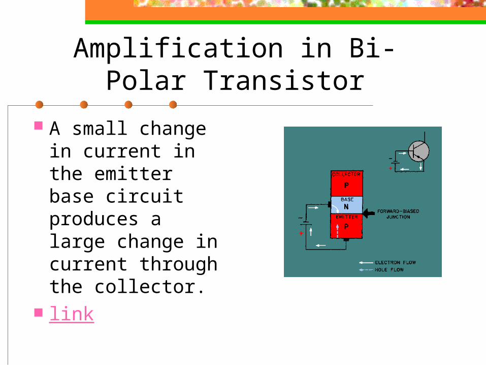
Amplification in Bi-Polar Transistor
A small change in current in the emitter base circuit produces a large change in current through the collector.
link
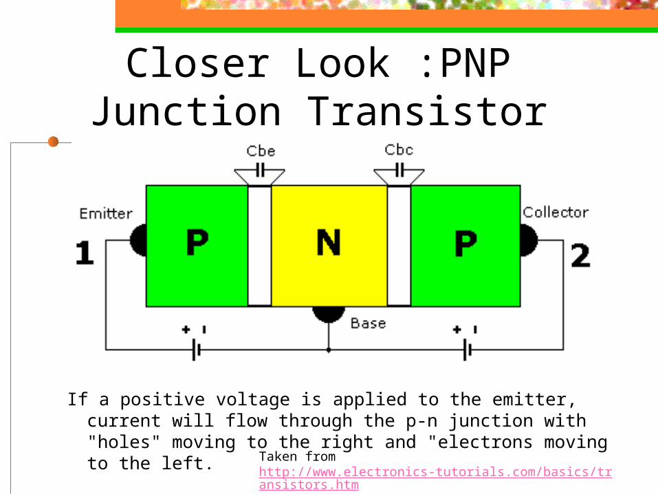
Closer Look :PNP Junction Transistor
If a positive voltage is applied to the emitter, current will flow through the p-n junction with "holes" moving to the right and "electrons moving to the left. Taken from
http://www.electronics-tutorials.com/basics/transistors.htm
Field Effect Transistors
weak electrical signal coming in through one electrode creates an electrical field through the rest of the transistor. This field flips from positive to negative when the incoming signal does, and controls a second current traveling through the rest of the transistor. The field modulates the second current to mimic the first one -- but it can be substantially larger.
From PBS.org http://www.pbs.org/transistor/science/info/transmodern.html
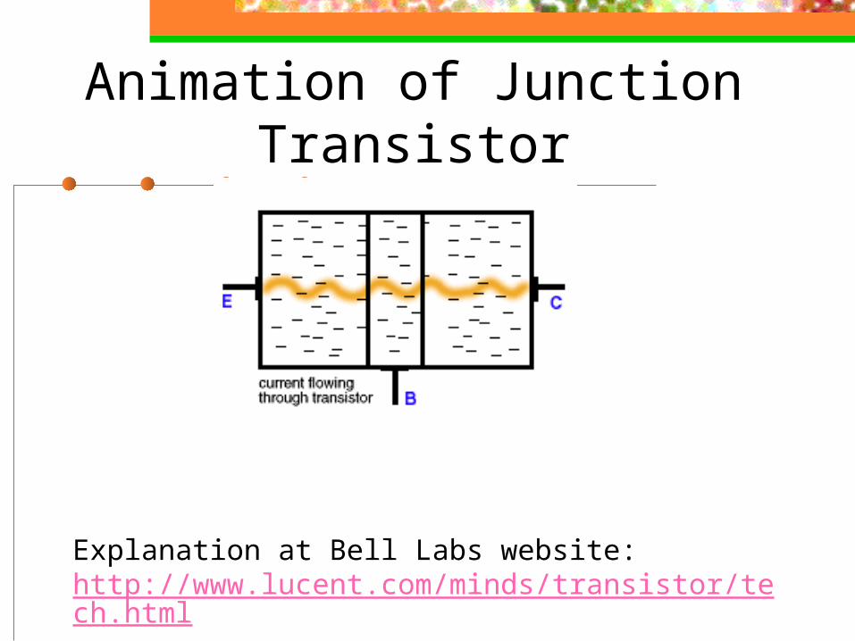
Animation of Junction Transistor
Explanation at Bell Labs website: http://www.lucent.com/minds/transistor/tech.html
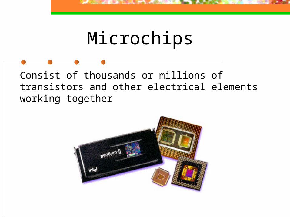
Microchips
Consist of thousands or millions of transistors and other electrical elements working together