Embed Size (px)
Citation preview

0.5
0.8
1
1.2
1.5
1.8
2
0 5 10 15 20 25 30 35Input Voltage (V)
Gro
und
Pin
Cur
rent
(µA
)
TA = −40°CTA = +25°CTA = +85°CTPS70912
G014
TPS709xx
EN
IN OUTVIN
VOUT
1 Fm 2.2 Fm
GND
NC
Product
Folder
Sample &Buy
Technical
Documents
Tools &
Software
Support &Community
TPS709SBVS186G –MARCH 2012–REVISED NOVEMBER 2015
TPS709 150-mA, 30-V, 1-µA IQ Voltage Regulators with Enable1 Features 3 Description
The TPS709 series of linear regulators are ultralow,1• Ultralow IQ: 1 μA
quiescent current devices designed for power-• Reverse Current Protection sensitive applications. A precision band-gap and error• Low ISHUTDOWN: 150 nA amplifier provides 2% accuracy over temperature.
Quiescent current of only 1 µA makes these devices• Input Voltage Range: 2.7 V to 30 Videal solutions for battery-powered, always-on• Supports 200-mA Peak Output systems that require very little idle-state power
• 2% Accuracy Over Temperature dissipation. These devices have thermal-shutdown,current-limit, and reverse-current protections for• Available in Fixed-Output Voltages:added safety.1.2 V to 6.5 V
• Thermal Shutdown and Overcurrent Protection Shutdown mode is enabled by pulling the EN pin low.The shutdown current in this mode goes down to 150• Packages: SOT-23-5, WSON-6nA, typical.
2 Applications The TPS709 series is available in WSON-6 andSOT-23-5 packages.• Zigbee™ Networks
• Home Automation Device Information(1)
• Metering PART NUMBER PACKAGE BODY SIZE (NOM)• Weighing Scales SOT-23 (5) 2.90 mm × 1.60 mm
TPS709• Portable Power Tools WSON (6) 2.00 mm × 2.00 mm• Remote Control Devices (1) For all available packages, see the package option addendum
at the end of the datasheet.• Wireless Handsets, Smart Phones, PDAs, WLAN,and Other PC Add-On Cards
• White Goods
Typical Application Circuit GND Current vs VIN and Temperature
1
An IMPORTANT NOTICE at the end of this data sheet addresses availability, warranty, changes, use in safety-critical applications,intellectual property matters and other important disclaimers. PRODUCTION DATA.

TPS709SBVS186G –MARCH 2012–REVISED NOVEMBER 2015 www.ti.com
Table of Contents1 Features .................................................................. 1 8 Application and Implementation ........................ 15
8.1 Application Information............................................ 152 Applications ........................................................... 18.2 Typical Application ................................................. 153 Description ............................................................. 1
9 Power Supply Recommendations ...................... 164 Revision History..................................................... 29.1 Power Dissipation ................................................... 165 Pin Configuration and Functions ......................... 4
10 Layout................................................................... 176 Specifications......................................................... 510.1 Layout Guidelines ................................................. 176.1 Absolute Maximum Ratings ...................................... 510.2 Layout Example .................................................... 176.2 ESD Ratings.............................................................. 5
11 Device and Documentation Support ................. 186.3 Recommended Operating Conditions....................... 511.1 Device Support...................................................... 186.4 Thermal Information .................................................. 511.2 Documentation Support ........................................ 186.5 Electrical Characteristics........................................... 611.3 Community Resources.......................................... 186.6 Typical Characteristics .............................................. 711.4 Trademarks ........................................................... 197 Detailed Description ............................................ 1311.5 Electrostatic Discharge Caution............................ 197.1 Overview ................................................................. 1311.6 Glossary ................................................................ 197.2 Functional Block Diagram ....................................... 13
12 Mechanical, Packaging, and Orderable7.3 Feature Description................................................. 13Information ........................................................... 197.4 Device Functional Modes........................................ 14
4 Revision HistoryNOTE: Page numbers for previous revisions may differ from page numbers in the current version.
Changes from Revision F (December 2014) to Revision G Page
• Added DBV package for TPS709A to Pin Configurations and Functions section.................................................................. 4• Added DBV package for TPS709B to Pin Configurations and Functions section.................................................................. 4• Added TPS709A and TPS709B to Pin Functions table ......................................................................................................... 4• Moved operating junction temperature from Electrical Characteristics to Recommended Operating Conditions ................. 5
Changes from Revision E (November 2013) to Revision F Page
• Changed title format to meet latest data sheet standards...................................................................................................... 1• Added ESD Rating table, Feature Description section, Device Functional Modes, Application and Implementation
section, Power Supply Recommendations section, Layout section, Device and Documentation Support section, andMechanical, Packaging, and Orderable Information section .................................................................................................. 1
• Deleted SOT-223-4 package from document ........................................................................................................................ 1• Deleted Low Dropout Features bullet .................................................................................................................................... 1• Changed Packages Feature bullet: deleted SOT-223-4 and footnote .................................................................................. 1• Deleted SOT-223-4 from last paragraph of Description section ........................................................................................... 1• Deleted pinout graphics from page 1 .................................................................................................................................... 1• Deleted DCY package and footnote from Pin Configurations section ................................................................................... 4• Changed Pin Functions table: changed title and deleted DCY package................................................................................ 4• Changed EN pin description in Pin Functions table .............................................................................................................. 4• Deleted the word 'range' from the last 2 rows of the Absolute Maximum Ratings table ........................................................ 5• Deleted DCY column from Thermal Information table ........................................................................................................... 5• Added description text to the enabled mode discussion in the Device Functional Modes section ..................................... 14
2 Submit Documentation Feedback Copyright © 2012–2015, Texas Instruments Incorporated
Product Folder Links: TPS709

TPS709www.ti.com SBVS186G –MARCH 2012–REVISED NOVEMBER 2015
Changes from Revision D (October 2013) to Revision E Page
• Changed DRV (SON-6) package status from Preview to Production Data............................................................................ 1• Deleted SON-6 package from footnote 1 in Features section................................................................................................ 1• Deleted DRV package from pinout diagram note................................................................................................................... 1• Deleted DRV from pinout note in the Pin Configurations section........................................................................................... 4
Changes from Revision C (June 2013) to Revision D Page
• Changed device status from Production Data to Mixed Status.............................................................................................. 1• Changed last Features bullet: added footnote and changed device order............................................................................. 1• Added note to pinout diagrams............................................................................................................................................... 1• Added product preview footnote to pin configurations ........................................................................................................... 4
Changes from Revision B (November 2012) to Revision C Page
• Added DCY (SOT-223) and DRV (SON) packages to data sheet ......................................................................................... 1• Changed IQ feature bullet value from 1.35 µA to 1 µA ........................................................................................................... 1• Changed quiescent current value in first paragraph of Description section from 1.35 µA to 1 µA ........................................ 1• Changed text in second paragraph of Description section from "leakage" to "shutdown." .................................................... 1• Added typical application circuit ............................................................................................................................................. 1• Added DCY and DRV packages to Pin Configuration section .............................................................................................. 4• Added DCY and DRV packages to Pin Descriptions table ................................................................................................... 4• Added DRV and DCY packages to Thermal Information table .............................................................................................. 5• Changed ground pin current typical values for IOUT = 0-mA test conditions........................................................................... 6
Changes from Revision A (October 2012) to Revision B Page
• Added Pin Configuration section ............................................................................................................................................ 4• Changed Line regulation and Load regulation parameters in Electrical Characteristics table............................................... 6• Changed IGND parameter test conditions in Electrical Characteristics table ........................................................................... 6• Changed ISHUTDOWN parameter test conditions in Electrical Characteristics table .................................................................. 6• Changed footnote 4 in Electrical Characteristics table........................................................................................................... 6• Changed second paragraph of Dropout Voltage section ..................................................................................................... 13
Changes from Original (March 2012) to Revision A Page
• Changed device status from Product Preview to Production Data ........................................................................................ 1
Copyright © 2012–2015, Texas Instruments Incorporated Submit Documentation Feedback 3
Product Folder Links: TPS709

EN
NC
OUT
GND
IN
1
2
3
5
4
IN
NC
EN
6
5
4
OUT
NC
GND
1
2
3
GN
D
EN
NC
GND
IN
OUT
1
2
3
5
4
OUT
NC
IN
GND
EN
1
2
3
5
4
TPS709SBVS186G –MARCH 2012–REVISED NOVEMBER 2015 www.ti.com
5 Pin Configuration and Functions
TPS709: DBV PackageTPS709B: DBV Package5-Pin SOT-23
5-Pin SOT-23Top ViewTop View
TPS709A: DBV PackageDRV Package5-Pin SOT-236-Pin WSONTop View
Top View
Pin FunctionsPIN
DRV DBV I/O DESCRIPTIONNAME TPS709 TPS709 TPS709A TPS709B
Enable pin. Drive this pin high to enable the device. Drive this pin lowto put the device into low current shutdown. This pin can be leftEN 4 3 5 5 I floating to enable the device. The maximum voltage must remainbelow 6.5 V.
GND 3 2 2 1 — GroundIN 6 1 3 2 I Unregulated input to the deviceNC 2, 5 4 4 4 — No internal connection
Regulated output voltage. Connect a small 2.2-µF or greater ceramicOUT 1 5 1 3 O capacitor from this pin to ground to assure stability.The thermal pad is electrically connected to the GND node. ConnectThermal pad — — — — this pad to the GND plane for improved thermal performance.
4 Submit Documentation Feedback Copyright © 2012–2015, Texas Instruments Incorporated
Product Folder Links: TPS709

TPS709www.ti.com SBVS186G –MARCH 2012–REVISED NOVEMBER 2015
6 Specifications
6.1 Absolute Maximum Ratingsspecified at TJ = –40°C to 125°C (unless otherwise noted); all voltages are with respect to GND (1)
MIN MAX UNITVIN –0.3 32
Voltage VEN –0.3 7 VVOUT –0.3 7
Maximum output current IOUT Internally limitedOutput short-circuit duration IndefiniteContinuous total power dissipation PDISS See Thermal InformationOperating junction temperature, TJ –55 150 °CStorage temperature, Tstg –55 150 °C
(1) Stresses beyond those listed under Absolute Maximum Ratings may cause permanent damage to the device. These are stress ratingsonly, which do not imply functional operation of the device at these or any other conditions beyond those indicated under RecommendedOperating Conditions. Exposure to absolute-maximum-rated conditions for extended periods may affect device reliability.
6.2 ESD RatingsVALUE UNIT
Human body model (HBM), per ANSI/ESDA/JEDEC JS-001 (1) ±2000V(ESD) Electrostatic discharge V
Charged device model (CDM), per JEDEC specification JESD22-C101 (2) ±500
(1) JEDEC document JEP155 states that 2-kV HBM allows safe manufacturing with a standard ESD control process.(2) JEDEC document JEP157 states that 500-V CDM allows safe manufacturing with a standard ESD control process.
6.3 Recommended Operating Conditionsover operating junction temperature range (unless otherwise noted)
MIN NOM MAX UNITVIN Input voltage 2.7 30 VVOUT Output voltage 1.2 6.5 VVEN Enable voltage 0 6.5 VTJ Operating junction temperature –40 125 °C
6.4 Thermal InformationTPS709
THERMAL METRIC (1) DBV DRV UNIT5 PINS 6 PINS
RθJA Junction-to-ambient thermal resistance 212.1 73.1 °C/WRθJC(top) Junction-to-case (top) thermal resistance 78.5 97.0 °C/WRθJB Junction-to-board thermal resistance 39.5 42.6 °C/WψJT Junction-to-top characterization parameter 2.86 2.9 °C/WψJB Junction-to-board characterization parameter 38.7 42.9 °C/WRθJC(bot) Junction-to-case (bottom) thermal resistance N/A 12.8 °C/W
(1) For more information about traditional and new thermal metrics, see the IC Package Thermal Metrics application report, SPRA953.
Copyright © 2012–2015, Texas Instruments Incorporated Submit Documentation Feedback 5
Product Folder Links: TPS709
TPS709SBVS186G –MARCH 2012–REVISED NOVEMBER 2015 www.ti.com
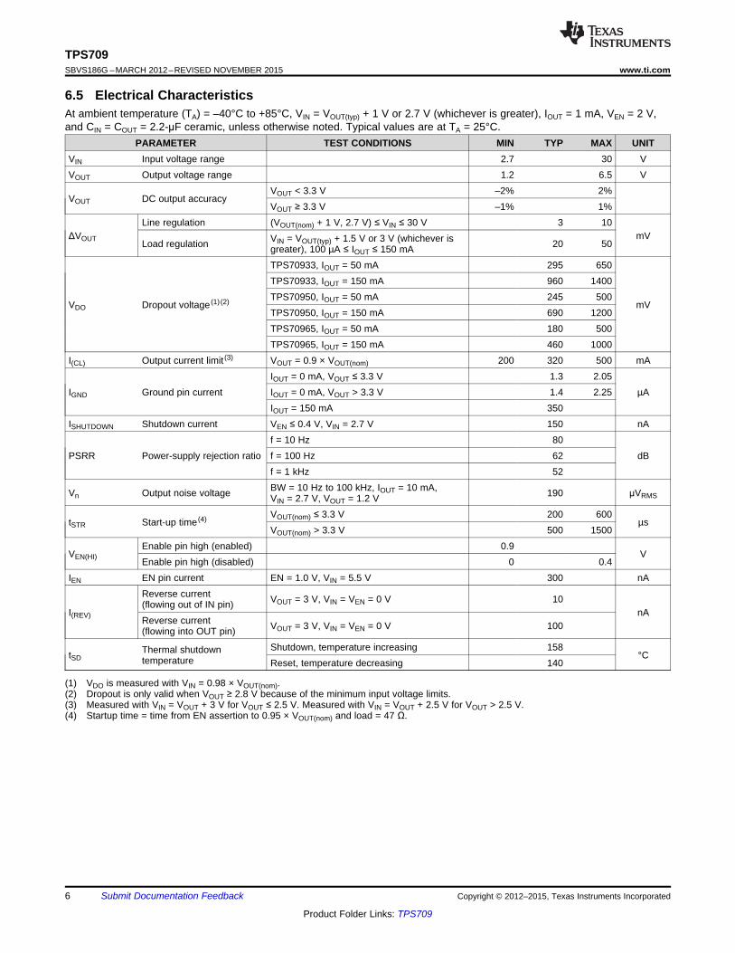
6.5 Electrical CharacteristicsAt ambient temperature (TA) = –40°C to +85°C, VIN = VOUT(typ) + 1 V or 2.7 V (whichever is greater), IOUT = 1 mA, VEN = 2 V,and CIN = COUT = 2.2-μF ceramic, unless otherwise noted. Typical values are at TA = 25°C.
PARAMETER TEST CONDITIONS MIN TYP MAX UNITVIN Input voltage range 2.7 30 VVOUT Output voltage range 1.2 6.5 V
VOUT < 3.3 V –2% 2%VOUT DC output accuracy
VOUT ≥ 3.3 V –1% 1%Line regulation (VOUT(nom) + 1 V, 2.7 V) ≤ VIN ≤ 30 V 3 10
ΔVOUT mVVIN = VOUT(typ) + 1.5 V or 3 V (whichever isLoad regulation 20 50greater), 100 µA ≤ IOUT ≤ 150 mATPS70933, IOUT = 50 mA 295 650TPS70933, IOUT = 150 mA 960 1400TPS70950, IOUT = 50 mA 245 500
VDO Dropout voltage (1) (2) mVTPS70950, IOUT = 150 mA 690 1200TPS70965, IOUT = 50 mA 180 500TPS70965, IOUT = 150 mA 460 1000
I(CL) Output current limit (3) VOUT = 0.9 × VOUT(nom) 200 320 500 mAIOUT = 0 mA, VOUT ≤ 3.3 V 1.3 2.05
IGND Ground pin current IOUT = 0 mA, VOUT > 3.3 V 1.4 2.25 µAIOUT = 150 mA 350
ISHUTDOWN Shutdown current VEN ≤ 0.4 V, VIN = 2.7 V 150 nAf = 10 Hz 80
PSRR Power-supply rejection ratio f = 100 Hz 62 dBf = 1 kHz 52BW = 10 Hz to 100 kHz, IOUT = 10 mA,Vn Output noise voltage 190 μVRMSVIN = 2.7 V, VOUT = 1.2 VVOUT(nom) ≤ 3.3 V 200 600
tSTR Start-up time (4) µsVOUT(nom) > 3.3 V 500 1500
Enable pin high (enabled) 0.9VEN(HI) V
Enable pin high (disabled) 0 0.4IEN EN pin current EN = 1.0 V, VIN = 5.5 V 300 nA
Reverse current VOUT = 3 V, VIN = VEN = 0 V 10(flowing out of IN pin)I(REV) nA
Reverse current VOUT = 3 V, VIN = VEN = 0 V 100(flowing into OUT pin)Shutdown, temperature increasing 158Thermal shutdowntSD °Ctemperature Reset, temperature decreasing 140
(1) VDO is measured with VIN = 0.98 × VOUT(nom).(2) Dropout is only valid when VOUT ≥ 2.8 V because of the minimum input voltage limits.(3) Measured with VIN = VOUT + 3 V for VOUT ≤ 2.5 V. Measured with VIN = VOUT + 2.5 V for VOUT > 2.5 V.(4) Startup time = time from EN assertion to 0.95 × VOUT(nom) and load = 47 Ω.
6 Submit Documentation Feedback Copyright © 2012–2015, Texas Instruments Incorporated
Product Folder Links: TPS709

3.275
3.28
3.285
3.29
3.295
3.3
3.305
0 20 40 60 80 100 120 140 160Output Current (mA)
Out
put V
olta
ge (
V)
TJ = −40°CTJ = +25°CTJ = +85°CTJ = +125°C
TPS70933
G005
6.46
6.465
6.47
6.475
6.48
6.485
6.49
6.495
6.5
6.505
0 20 40 60 80 100 120 140 160Output Current (mA)
Out
put V
olta
ge (
V)
TJ = −40°CTJ = +25°CTJ = +85°CTJ = +125°C
TPS70965
G006
6.49
6.495
6.5
6.505
6.51
5 10 15 20 25 30Input Voltage (V)
Out
put V
olta
ge (
V)
TJ = −40°CTJ = +25°CTJ = +85°CTJ = +125°C
TPS70965
G003
1.18
1.185
1.19
1.195
1.2
1.205
0 20 40 60 80 100 120 140 160Output Current (mA)
Out
put V
olta
ge (
V)
TJ = −40°CTJ = +25°CTJ = +85°CTJ = +125°C
TPS70912
G004
1.195
1.2
1.205
0 5 10 15 20 25 30Input Voltage (V)
Out
put V
olta
ge (
V)
TJ = −40°CTJ = +25°CTJ = +85°CTJ = +125°C
TPS70912
G001
3.29
3.295
3.3
3.305
3.31
0 5 10 15 20 25 30Input Voltage (V)
Out
put V
olta
ge (
V)
TJ = −40°CTJ = +25°CTJ = +85°CTJ = +125°C
TPS70933
G002
TPS709www.ti.com SBVS186G –MARCH 2012–REVISED NOVEMBER 2015
6.6 Typical CharacteristicsOver operating temperature range (TJ = –40°C to 125°C), IOUT = 10 mA, VEN = 2 V, COUT = 2.2 μF, and VIN = VOUT(typ) + 1 V or2.7 V (whichever is greater), unless otherwise noted. Typical values are at TJ = 25°C.
Figure 1. 1.2-V Line Regulation vs VIN and Temperature Figure 2. 3.3-V Line Regulation vs VIN and Temperature
Figure 3. 6.5-V Line Regulation vs VIN and Temperature Figure 4. 1.2-V Load Regulation vs IOUT and Temperature
Figure 5. 3.3-V Load Regulation vs IOUT and Temperature Figure 6. 6.5-V Load Regulation vs IOUT and Temperature
Copyright © 2012–2015, Texas Instruments Incorporated Submit Documentation Feedback 7
Product Folder Links: TPS709

200
250
300
350
400
450
500
3 3.5 4 4.5 5 5.5 6 6.5 7Input Voltage (V)
Cur
rent
Lim
it (m
A)
TJ = −40°CTJ = +25°CTJ = +85°CTJ = +125°C
TPS70912
G011
300
350
400
450
500
5 5.5 6 6.5 7 7.5 8 8.5Input Voltage (V)
Cur
rent
Lim
it (m
A)
TJ = −40°CTJ = +25°CTJ = +85°CTJ = +125°C
TPS70933
G012
0
200
400
600
800
1000
1200
1400
1600
2.5 3.5 4.5 5.5 6.5Input Voltage (V)
Dro
pout
Vol
tage
(m
V)
TJ = −40°CTJ = +25°CTJ = +85°CTJ = +125°C
TPS70965IOUT = 150 mA
G009
0
200
400
600
800
1000
1200
1400
1600
0 20 40 60 80 100 120 140 160Output Current (mA)
Dro
pout
Vol
tage
(m
V)
TJ = −40°CTJ = +25°CTJ = +85°CTJ = +125°C
TPS70965
G010
1.18
1.185
1.19
1.195
1.2
1.205
−50 −35 −20 −5 10 25 40 55 70 85 100 115 130Junction Temperature (°C)
Out
put V
olta
ge (
V)
IOUT = 10 mAIOUT = 150 mA
TPS70912
G007
6.465
6.47
6.475
6.48
6.485
6.49
6.495
6.5
6.505
−50 −35 −20 −5 10 25 40 55 70 85 100 115 130Junction Temperature (°C)
Out
put V
olta
ge (
V)
IOUT = 10 mAIOUT = 150 mA
TPS70965
G008
TPS709SBVS186G –MARCH 2012–REVISED NOVEMBER 2015 www.ti.com
Typical Characteristics (continued)Over operating temperature range (TJ = –40°C to 125°C), IOUT = 10 mA, VEN = 2 V, COUT = 2.2 μF, and VIN = VOUT(typ) + 1 V or2.7 V (whichever is greater), unless otherwise noted. Typical values are at TJ = 25°C.
Figure 7. VOUT vs Temperature Figure 8. VOUT vs Temperature
Figure 9. Dropout Voltage vs VIN and Temperature Figure 10. Dropout Voltage vs IOUT and Temperature
Figure 11. 1.2-V Current Limit vs VIN and Temperature Figure 12. 3.3-V Current Limit vs VIN and Temperature
8 Submit Documentation Feedback Copyright © 2012–2015, Texas Instruments Incorporated
Product Folder Links: TPS709
0
0.1
0.2
0.3
0.4
0 5 10 15 20 25 30 35Input Voltage (V)
Gro
und
Pin
Cur
rent
(µA
)
TA = −40°CTA = +25°CTA = +85°C
Shutdown CurrentTPS70912
G016
0
20
40
60
80
100
10 100 1k 10k 100k 1M 10MFrequency (Hz)
PS
RR
(dB
)
VOUT = 2.8 VVIN = 3.8 VCOUT = 2.2 µF
G017
0.5
0.75
1
1.25
1.5
1.75
2
2.25
2.5
0 5 10 15 20 25 30 35Input Voltage (V)
Gro
und
Pin
Cur
rent
(µA
)
TA = −40°CTA = +25°CTA = +85°C
TPS70933EN = open
G035
0
100
200
300
400
500
600
0 20 40 60 80 100 120 140 160Output Current (mA)
Gro
und
Pin
Cur
rent
(µA
)
TA = −40°CTA = +25°CTA = +85°C
TPS70912
G015
300
350
400
450
500
8 8.5 9 9.5 10 10.5 11 11.5 12Input Voltage (V)
Cur
rent
Lim
it (m
A)
TJ = −40°CTJ = +25°CTJ = +85°CTJ = +125°C
TPS70965
G013
0.5
0.8
1
1.2
1.5
1.8
2
0 5 10 15 20 25 30 35Input Voltage (V)
Gro
und
Pin
Cur
rent
(µA
)
TA = −40°CTA = +25°CTA = +85°CTPS70912
G014
TPS709www.ti.com SBVS186G –MARCH 2012–REVISED NOVEMBER 2015
Typical Characteristics (continued)Over operating temperature range (TJ = –40°C to 125°C), IOUT = 10 mA, VEN = 2 V, COUT = 2.2 μF, and VIN = VOUT(typ) + 1 V or2.7 V (whichever is greater), unless otherwise noted. Typical values are at TJ = 25°C.
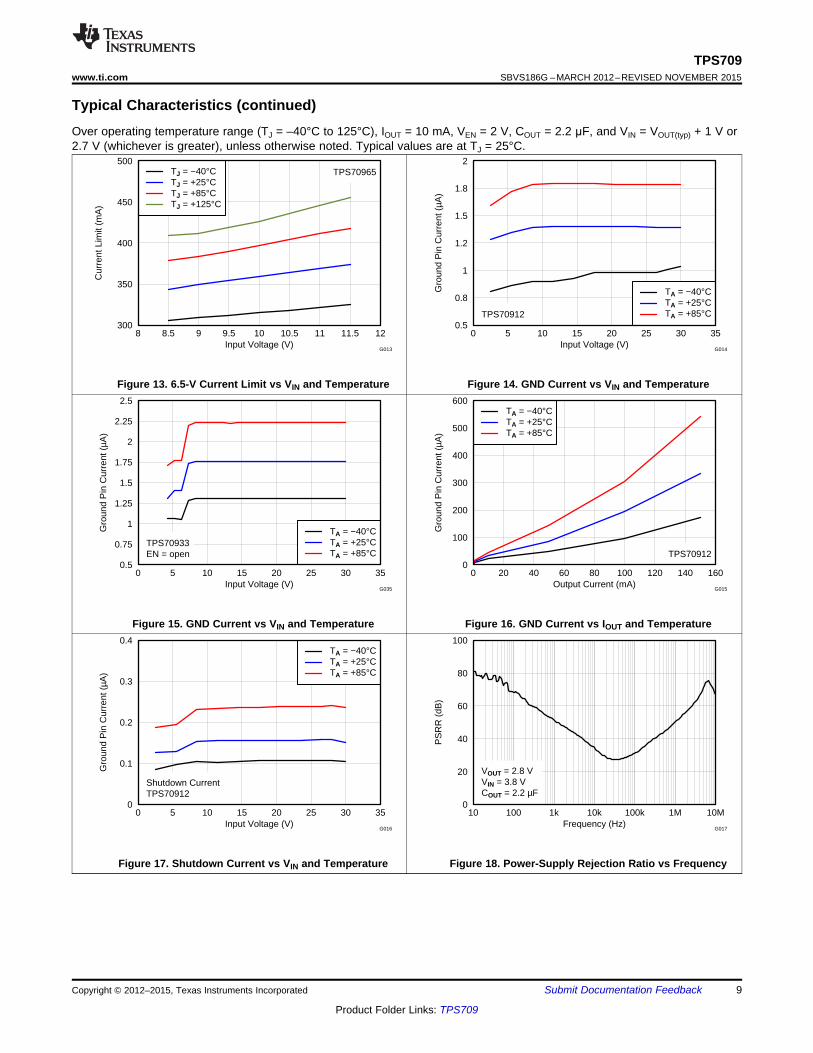
Figure 13. 6.5-V Current Limit vs VIN and Temperature Figure 14. GND Current vs VIN and Temperature
Figure 15. GND Current vs VIN and Temperature Figure 16. GND Current vs IOUT and Temperature
Figure 17. Shutdown Current vs VIN and Temperature Figure 18. Power-Supply Rejection Ratio vs Frequency
Copyright © 2012–2015, Texas Instruments Incorporated Submit Documentation Feedback 9
Product Folder Links: TPS709

Channel 4(50 mA / div)
Channel 2(200 mV / div)
Time (10 ms / div)
Channel 2 = V
Channel 4 = I
V = 2.7 V
OUT
OUT
IN
G022
Channel 4(100 mA / div)
Channel 2(200 mV / div)
Time (100 s / div)m
Channel 2 = V
4 = I
V = 2.7 V
OUT
OUT
IN
Channel
G023
Channel 4(50 mA / div)
Channel 2(200 mV / div)
Time (100 s / div)m
Channel 2 = V
Channel 4 = I
V = 2.7 V
OUT
OUT
IN
G020
Channel 4(100 mA / div)
Channel 2(200 mV / div)
Time (500 s / div)m
Channel 2 = V
Channel 4 = I
V = 2.7 V
OUT
OUT
IN
G021
0
1
2
3
4
5
6
7
10 100 1k 10k 100kFrequency (Hz)
Vol
tage
( µV
/ H
z )
VOUT = 2.8 V
G018
100
110
120
130
140
−50 −35 −20 −5 10 25 40 55 70 85 100 115 130Temperature (°C)
Tim
e (µ
s)
TPS70912
G019
TPS709SBVS186G –MARCH 2012–REVISED NOVEMBER 2015 www.ti.com
Typical Characteristics (continued)Over operating temperature range (TJ = –40°C to 125°C), IOUT = 10 mA, VEN = 2 V, COUT = 2.2 μF, and VIN = VOUT(typ) + 1 V or2.7 V (whichever is greater), unless otherwise noted. Typical values are at TJ = 25°C.
Figure 19. Noise Figure 20. Start-Up Time vs Temperature
Figure 21. TPS70912 Load Transient (0 mA to 50 mA) Figure 22. TPS70912 Load Transient (1 mA to 150 mA)
Figure 23. TPS70912 Load Transient (50 mA to 0 mA) Figure 24. TPS70912 Load Transient (50 mA to 150 mA)
10 Submit Documentation Feedback Copyright © 2012–2015, Texas Instruments Incorporated
Product Folder Links: TPS709

Channel 4(2 V / div)
Channel 2(50 mV / div)
Time (50 s / div)m
G028
Channel 2 = V
4 = V
I = 10 mA
OUT
IN
OUT
Channel
Channel 4(2 V / div)
Channel 2(50 mV / div)
Time (50 s / div)m
G029
Channel 2 = V
4 = V
I = 50 mA
OUT
IN
OUT
Channel
Channel 4(50 mA / div)
Channel 2(200 mV / div)
Time (10 ms / div)
Channel 2 = V
Channel 4 = I
V = 4.3 V
OUT
OUT
IN
G026
Channel 4(50 mA / div)
Channel 2(200 mV / div)
Time (500 s / div)m
Channel 2 = V
Channel 4 = I
V = 4.3 V
OUT
OUT
IN
G027
Channel 4(50 mA / div)
Channel 2(200 mV / div)
Time (100 s / div)m
Channel 2 = V
Channel 4 = I
V = 4.3 V
OUT
OUT
IN
G024
Channel 4(100 mA / div)
Channel 2(200 mV / div)
Time (500 s / div)m
Channel 2 = V
Channel 4 = I
V = 4.3 V
OUT
OUT
IN
G025
TPS709www.ti.com SBVS186G –MARCH 2012–REVISED NOVEMBER 2015
Typical Characteristics (continued)Over operating temperature range (TJ = –40°C to 125°C), IOUT = 10 mA, VEN = 2 V, COUT = 2.2 μF, and VIN = VOUT(typ) + 1 V or2.7 V (whichever is greater), unless otherwise noted. Typical values are at TJ = 25°C.
Figure 25. TPS70933 Load Transient (0 mA to 50 mA) Figure 26. TPS70933 Load Transient (1 mA to 150 mA)
Figure 27. TPS70933 Load Transient (50 mA to 0 mA) Figure 28. TPS70933 Load Transient (50 mA to 150 mA)
Figure 29. TPS70912 Line Transient (2.7 V to 3.7 V) Figure 30. TPS70912 Line Transient (2.7 V to 3.7 V)
Copyright © 2012–2015, Texas Instruments Incorporated Submit Documentation Feedback 11
Product Folder Links: TPS709

Channel 2(1 V / div)
Channel 1(1 V / div)
Time (500 ms / div)
G034
Channel 1 = V
2 = V
I = 150 mA
TPS70933
IN
OUT
Channel OUT
Channel 2(1 V / div)
Channel 1(500 mV / div)
Time (50 s / div)m
G032
Channel 1 = EN2 = V
V = 4.3 V
C = 2.2 F
TPS70933
Channel OUT
IN
OUT m
Channel 2(1 V / div)
Channel 1(1 V / div)
Time (500 ms / div)
G033
Channel 1 = V
2 = V
I = 3 mA
TPS70933
IN
OUT
Channel OUT
Channel 4(2 V / div)
Channel 2(50 mV / div)
Time (50 s / div)m
G030
Channel 2 = V
4 = V
I = 10 mA
OUT
IN
OUT
Channel
Channel 4(2 V / div)
Channel 2(50 mV / div)
Time (50 s / div)m
G031
Channel 2 = V
4 = V
I = 50 mA
OUT
IN
OUT
Channel
TPS709SBVS186G –MARCH 2012–REVISED NOVEMBER 2015 www.ti.com
Typical Characteristics (continued)Over operating temperature range (TJ = –40°C to 125°C), IOUT = 10 mA, VEN = 2 V, COUT = 2.2 μF, and VIN = VOUT(typ) + 1 V or2.7 V (whichever is greater), unless otherwise noted. Typical values are at TJ = 25°C.
Figure 31. TPS70933 Line Transient (4.3 V to 5.3 V) Figure 32. TPS70933 Line Transient (4.3 V to 5.3 V)
Figure 33. Power-Up with Enable Figure 34. Power-Up and Power-Down Response
Figure 35. Power-Up and Power-Down Response
12 Submit Documentation Feedback Copyright © 2012–2015, Texas Instruments Incorporated
Product Folder Links: TPS709
ThermalShutdown
CurrentLimit
Bandgap
IN
EN
OUT
Logic
GND
Device
TPS709www.ti.com SBVS186G –MARCH 2012–REVISED NOVEMBER 2015
7 Detailed Description
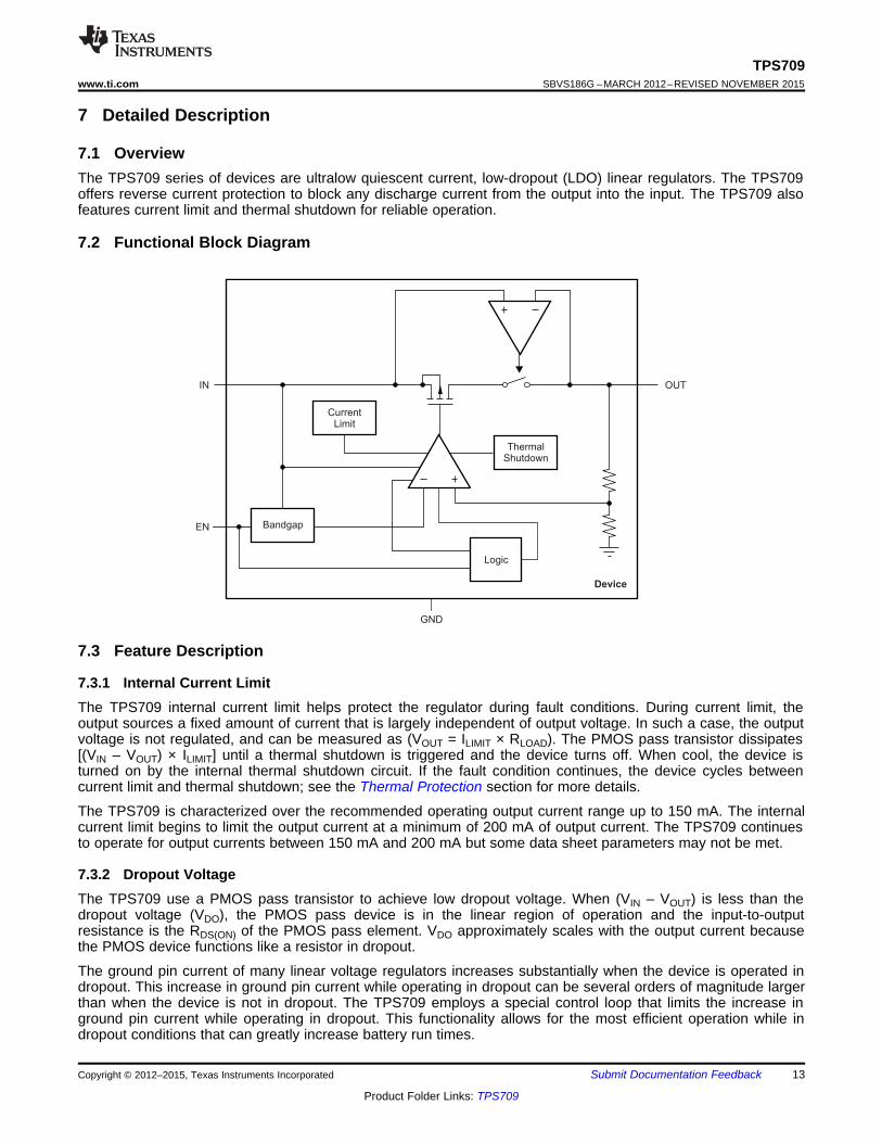
7.1 OverviewThe TPS709 series of devices are ultralow quiescent current, low-dropout (LDO) linear regulators. The TPS709offers reverse current protection to block any discharge current from the output into the input. The TPS709 alsofeatures current limit and thermal shutdown for reliable operation.
7.2 Functional Block Diagram
7.3 Feature Description
7.3.1 Internal Current LimitThe TPS709 internal current limit helps protect the regulator during fault conditions. During current limit, theoutput sources a fixed amount of current that is largely independent of output voltage. In such a case, the outputvoltage is not regulated, and can be measured as (VOUT = ILIMIT × RLOAD). The PMOS pass transistor dissipates[(VIN – VOUT) × ILIMIT] until a thermal shutdown is triggered and the device turns off. When cool, the device isturned on by the internal thermal shutdown circuit. If the fault condition continues, the device cycles betweencurrent limit and thermal shutdown; see the Thermal Protection section for more details.
The TPS709 is characterized over the recommended operating output current range up to 150 mA. The internalcurrent limit begins to limit the output current at a minimum of 200 mA of output current. The TPS709 continuesto operate for output currents between 150 mA and 200 mA but some data sheet parameters may not be met.
7.3.2 Dropout VoltageThe TPS709 use a PMOS pass transistor to achieve low dropout voltage. When (VIN – VOUT) is less than thedropout voltage (VDO), the PMOS pass device is in the linear region of operation and the input-to-outputresistance is the RDS(ON) of the PMOS pass element. VDO approximately scales with the output current becausethe PMOS device functions like a resistor in dropout.
The ground pin current of many linear voltage regulators increases substantially when the device is operated indropout. This increase in ground pin current while operating in dropout can be several orders of magnitude largerthan when the device is not in dropout. The TPS709 employs a special control loop that limits the increase inground pin current while operating in dropout. This functionality allows for the most efficient operation while indropout conditions that can greatly increase battery run times.
Copyright © 2012–2015, Texas Instruments Incorporated Submit Documentation Feedback 13
Product Folder Links: TPS709

TPS709SBVS186G –MARCH 2012–REVISED NOVEMBER 2015 www.ti.com
Feature Description (continued)7.3.3 Undervoltage Lockout (UVLO)The TPS709 uses an undervoltage lockout (UVLO) circuit to keep the output shut off until the internal circuitryoperates properly.
7.3.4 Reverse-Current ProtectionThe TPS709 has integrated reverse-current protection. Reverse-current protection prevents the flow of currentfrom the OUT pin to the IN pin when output voltage is higher than input voltage. The reverse-current protectioncircuitry places the power path in high impedance when the output voltage is higher than the input voltage. Thissetting reduces leakage current from the output to the input to 10 nA, typical. The reverse current protection isalways active regardless of the enable pin logic state or if the OUT pin voltage is greater than 1.8 V. Reversecurrent can flow if the output voltage is less than 1.8 V and if input voltage is less than the output voltage.
If voltage is applied to the input pin, then the maximum voltage that can be applied to the OUT pin is the lower ofthree times the nominal output voltage or 6.5 V. For example, if the 1.2-V output voltage version is used, then themaximum reverse bias voltage that can be applied to the OUT pin is 3.6 V. If the 5.0-V output voltage version isused, then the maximum reverse bias voltage that can be applied to the OUT pin is 6.5 V.
7.4 Device Functional ModesThe TPS709 has the following functional modes:1. Enabled: When the enable pin (EN) goes above 0.9 V, the device is enabled. EN is pulled high by a 300-nA
current source; therefore, EN can be left floating to enable the device. Do not connect EN to VIN. The EN pinis clamped by a 6.5-V Zener diode. Do not exceed the 7-V absolute maximum rating on the enable pin orexcessive current flowing into the Zener clamp will destroy the device.
2. Disabled: When EN goes below 0.4 V, the device is disabled. During this time, OUT is high impedance andthe current into IN (I(SHUTDOWN)) is typically 150 nA.
14 Submit Documentation Feedback Copyright © 2012–2015, Texas Instruments Incorporated
Product Folder Links: TPS709

TPS70933
EN
IN OUTVIN
VOUT
1 Fm 2.2 Fm
GND
NC
TPS709www.ti.com SBVS186G –MARCH 2012–REVISED NOVEMBER 2015
8 Application and Implementation
NOTEInformation in the following applications sections is not part of the TI componentspecification, and TI does not warrant its accuracy or completeness. TI’s customers areresponsible for determining suitability of components for their purposes. Customers shouldvalidate and test their design implementation to confirm system functionality.
8.1 Application InformationThe TPS709 is a series of devices that belong to a new family of next-generation voltage regulators. Thesedevices consume low quiescent current and deliver excellent line and load transient performance. Thisperformance, combined with low noise and very good PSRR with little (VIN – VOUT) headroom, makes thesedevices ideal for RF portable applications, current limit, and thermal protection. The TPS709 is specified from–40°C to +125°C.
8.1.1 Input and Output CapacitorThe TPS709 devices are stable with output capacitors with an effective capacitance of 2.0 μF or greater foroutput voltages below 1.5 V. For output voltages equal or greater than 1.5 V, the minimum effective capacitancefor stability is 1.5 µF. The maximum capacitance for stability is 47 µF. The equivalent series resistance (ESR) ofthe output capacitor must be between 0 Ω and 0.2 Ω for stability.
The effective capacitance is the minimum capacitance value of a capacitor after taking into account variationsresulting from tolerances, temperature, and dc bias effects. X5R- and X7R-type ceramic capacitors arerecommended because these capacitors have minimal variation in value and ESR over temperature.
Although an input capacitor is not required for stability, good analog design practice is to connect a 0.1-µF to2.2-µF capacitor from IN to GND. This capacitor counteracts reactive input sources and improves transientresponse, input ripple, and PSRR. An input capacitor is necessary if line transients greater than 10 V inmagnitude are anticipated.
8.1.2 Transient ResponseAs with any regulator, increasing the output capacitor size reduces over- and undershoot magnitude, butincreases transient response duration.
8.2 Typical Application
Figure 36. Wide Input, 3.3-V, Low-IQ Rail
8.2.1 Design RequirementsTable 1 summarizes the design requirements for Figure 36.
Table 1. Design Requirements for a Wide Input, 3.3-V, Low-IQ Rail ApplicationPARAMETER DESIGN SPECIFICATION
VIN 5 V to 20 VVOUT 3.3 V
I(IN) (no load) < 5 µAIOUT (max) 150 mA
Copyright © 2012–2015, Texas Instruments Incorporated Submit Documentation Feedback 15
Product Folder Links: TPS709

Channel 4(50 mA / div)
Channel 2(200 mV / div)
Time (500 s / div)m
Channel 2 = V
Channel 4 = I
V = 4.3 V
OUT
OUT
IN
G027
Channel 2(1 V / div)
Channel 1(500 mV / div)
Time (50 s / div)m
G032
Channel 1 = EN2 = V
V = 4.3 V
C = 2.2 F
TPS70933
Channel OUT
IN
OUT m
TPS709SBVS186G –MARCH 2012–REVISED NOVEMBER 2015 www.ti.com
8.2.2 Detailed Design ProcedureSelect a 2.2-µF, 10-V X7R output capacitor to satisfy the minimum output capacitance requirement with a 3.3-Vdc bias.
Select a 1.0-µF, 25-V X7R input capacitor to provide input noise filtering and eliminate high-frequency voltagetransients.
8.2.3 Application Curves
Figure 37. TPS70933 Load Transient (50 mA to 150 mA) Figure 38. Power-Up with Enable
9 Power Supply RecommendationsThis device is designed to operate with an input supply range of 2.7 V to 30 V. If the input supply is noisy,additional input capacitors with low ESR can help improve output noise performance.
9.1 Power DissipationThe ability to remove heat from the die is different for each package type, presenting different considerations inthe printed circuit board (PCB) layout. The PCB area around the device that is free of other components movesthe heat from the device to ambient air. Performance data for JEDEC low and high-K boards are given in theThermal Information table. Using heavier copper increases the effectiveness in removing heat from the device.The addition of plated through-holes to heat-dissipating layers also improves the heatsink effectiveness.
Power dissipation depends on input voltage and load conditions. Power dissipation (PDISS) is equal to the productof the output current and the voltage drop across the output pass element, as shown in Equation 1:
PDISS = (VIN – VOUT) × IOUT (1)
16 Submit Documentation Feedback Copyright © 2012–2015, Texas Instruments Incorporated
Product Folder Links: TPS709

COUT
VOUTVIN
GND PLANE
CIN
Represents via used for application specific connections
1
2
3 4
5
TPS709www.ti.com SBVS186G –MARCH 2012–REVISED NOVEMBER 2015
10 Layout
10.1 Layout GuidelinesPlace input and output capacitors as close to the device pins as possible. To improve ac performance (such asPSRR, output noise, and transient response), TI recommends that the board be designed with separate groundplanes for VIN and VOUT, with the ground plane connected only at the GND pin of the device. In addition, theground connection for the output capacitor must be connected directly to the device GND pin.
10.1.1 Thermal ProtectionThermal protection disables the output when the junction temperature rises to approximately 165°C, allowing thedevice to cool. When the junction temperature cools to approximately 145°C, the output circuitry is againenabled. Depending on power dissipation, thermal resistance, and ambient temperature, the thermal protectioncircuit can cycle on and off. This cycling limits the dissipation of the regulator, protecting it from damage as aresult of overheating.
Any tendency to activate the thermal protection circuit indicates excessive power dissipation or an inadequateheatsink. For reliable operation, limit junction temperature to 125°C, maximum. To estimate the margin of safetyin a complete design (including heatsink), increase the ambient temperature until the thermal protection istriggered; use worst-case loads and signal conditions. For good reliability, thermal protection must trigger at least35°C above the maximum expected ambient condition of the particular application. This configuration produces aworst-case junction temperature of 125°C at the highest expected ambient temperature and worst-case load.
The TPS709 internal protection circuitry is designed to protect against overload conditions. This circuitry is notintended to replace proper heatsinking. Continuously running the TPS709 into thermal shutdown degradesdevice reliability.
10.2 Layout Example
Figure 39. Layout Example for DBV Package
Copyright © 2012–2015, Texas Instruments Incorporated Submit Documentation Feedback 17
Product Folder Links: TPS709
TPS709SBVS186G –MARCH 2012–REVISED NOVEMBER 2015 www.ti.com
11 Device and Documentation Support
11.1 Device Support
11.1.1 Development Support
11.1.1.1 Evaluation ModulesAn evaluation module (EVM) is available to assist in the initial circuit performance evaluation using theTPS709xx. The TPS70933EVM-110 evaluation module (and related user guide) can be requested at the TexasInstruments website through the product folders or purchased directly from the TI eStore.
11.1.1.2 Spice ModelsComputer simulation of circuit performance using SPICE is often useful when analyzing the performance ofanalog circuits and systems. A SPICE model for the TPS709 is available through the product folders underSimulation Models.
11.1.2 Device Nomenclature
Table 2. Device Nomenclature (1)
PRODUCT VOUT
TPS709xx(x)yyyz XX(X) is the nominal output voltage. For output voltages with a resolution of 100 mV, twodigits are used in the ordering number; otherwise, three digits are used (for example, 28 =2.8 V; 125 = 1.25 V).YYY is the package designator.Z is the tape and reel quantity (R = 3000, T = 250).
(1) For the most current package and ordering information see the Package Option Addendum at the end of this document, or see the TIweb site at www.ti.com.
11.2 Documentation Support
11.2.1 Related Documentation• TPS70933EVM-110 Evaluation Module User Guide, SLVU689
11.3 Community ResourcesThe following links connect to TI community resources. Linked contents are provided "AS IS" by the respectivecontributors. They do not constitute TI specifications and do not necessarily reflect TI's views; see TI's Terms ofUse.
TI E2E™ Online Community TI's Engineer-to-Engineer (E2E) Community. Created to foster collaborationamong engineers. At e2e.ti.com, you can ask questions, share knowledge, explore ideas and helpsolve problems with fellow engineers.
Design Support TI's Design Support Quickly find helpful E2E forums along with design support tools andcontact information for technical support.
18 Submit Documentation Feedback Copyright © 2012–2015, Texas Instruments Incorporated
Product Folder Links: TPS709

TPS709www.ti.com SBVS186G –MARCH 2012–REVISED NOVEMBER 2015
11.4 TrademarksE2E is a trademark of Texas Instruments.Zigbee is a trademark of ZigBee Alliance.All other trademarks are the property of their respective owners.
11.5 Electrostatic Discharge CautionThis integrated circuit can be damaged by ESD. Texas Instruments recommends that all integrated circuits be handled withappropriate precautions. Failure to observe proper handling and installation procedures can cause damage.
ESD damage can range from subtle performance degradation to complete device failure. Precision integrated circuits may be moresusceptible to damage because very small parametric changes could cause the device not to meet its published specifications.
11.6 GlossarySLYZ022 — TI Glossary.
This glossary lists and explains terms, acronyms, and definitions.
12 Mechanical, Packaging, and Orderable InformationThe following pages include mechanical, packaging, and orderable information. This information is the mostcurrent data available for the designated devices. This data is subject to change without notice and revision ofthis document. For browser-based versions of this data sheet, refer to the left-hand navigation.
Copyright © 2012–2015, Texas Instruments Incorporated Submit Documentation Feedback 19
Product Folder Links: TPS709

PACKAGE OPTION ADDENDUM
www.ti.com 24-Nov-2017
Addendum-Page 1
PACKAGING INFORMATION
Orderable Device Status(1)
Package Type PackageDrawing
Pins PackageQty
Eco Plan(2)
Lead/Ball Finish(6)
MSL Peak Temp(3)
Op Temp (°C) Device Marking(4/5)
Samples
TPS70912DBVR ACTIVE SOT-23 DBV 5 3000 Green (RoHS& no Sb/Br)
CU NIPDAU Level-1-260C-UNLIM -40 to 125 SCX
TPS70912DBVT ACTIVE SOT-23 DBV 5 250 Green (RoHS& no Sb/Br)
CU NIPDAU Level-1-260C-UNLIM -40 to 125 SCX
TPS70912DRVR ACTIVE WSON DRV 6 3000 Green (RoHS& no Sb/Br)
CU NIPDAU Level-1-260C-UNLIM -40 to 125 SCX
TPS70912DRVT ACTIVE WSON DRV 6 250 Green (RoHS& no Sb/Br)
CU NIPDAU Level-1-260C-UNLIM -40 to 125 SCX
TPS709135DBVR ACTIVE SOT-23 DBV 5 3000 Green (RoHS& no Sb/Br)
CU NIPDAU Level-1-260C-UNLIM -40 to 125 SCY
TPS709135DBVT ACTIVE SOT-23 DBV 5 250 Green (RoHS& no Sb/Br)
CU NIPDAU Level-1-260C-UNLIM -40 to 125 SCY
TPS70915DBVR ACTIVE SOT-23 DBV 5 3000 Green (RoHS& no Sb/Br)
CU NIPDAU Level-1-260C-UNLIM -40 to 125 SIM
TPS70915DBVT ACTIVE SOT-23 DBV 5 250 Green (RoHS& no Sb/Br)
CU NIPDAU Level-1-260C-UNLIM -40 to 125 SIM
TPS70915DRVR ACTIVE WSON DRV 6 3000 Green (RoHS& no Sb/Br)
CU NIPDAU Level-1-260C-UNLIM -40 to 125 SIM
TPS70915DRVT ACTIVE WSON DRV 6 250 Green (RoHS& no Sb/Br)
CU NIPDAU Level-1-260C-UNLIM -40 to 125 SIM
TPS70916DBVR ACTIVE SOT-23 DBV 5 3000 Green (RoHS& no Sb/Br)
CU NIPDAU Level-1-260C-UNLIM -40 to 125 SCZ
TPS70916DBVT ACTIVE SOT-23 DBV 5 250 Green (RoHS& no Sb/Br)
CU NIPDAU Level-1-260C-UNLIM -40 to 125 SCZ
TPS70918DBVR ACTIVE SOT-23 DBV 5 3000 Green (RoHS& no Sb/Br)
CU NIPDAU Level-1-260C-UNLIM -40 to 125 SDA
TPS70918DBVT ACTIVE SOT-23 DBV 5 250 Green (RoHS& no Sb/Br)
CU NIPDAU Level-1-260C-UNLIM -40 to 125 SDA
TPS70918DRVR ACTIVE WSON DRV 6 3000 Green (RoHS& no Sb/Br)
CU NIPDAU Level-1-260C-UNLIM -40 to 125 SDA
TPS70918DRVT ACTIVE WSON DRV 6 250 Green (RoHS& no Sb/Br)
CU NIPDAU Level-1-260C-UNLIM -40 to 125 SDA
TPS70919DBVR ACTIVE SOT-23 DBV 5 3000 Green (RoHS& no Sb/Br)
CU NIPDAU Level-1-260C-UNLIM -40 to 125 SDB

PACKAGE OPTION ADDENDUM
www.ti.com 24-Nov-2017
Addendum-Page 2
Orderable Device Status(1)
Package Type PackageDrawing
Pins PackageQty
Eco Plan(2)
Lead/Ball Finish(6)
MSL Peak Temp(3)
Op Temp (°C) Device Marking(4/5)
Samples
TPS70919DBVT ACTIVE SOT-23 DBV 5 250 Green (RoHS& no Sb/Br)
CU NIPDAU Level-1-260C-UNLIM -40 to 125 SDB
TPS70925DBVR ACTIVE SOT-23 DBV 5 3000 Green (RoHS& no Sb/Br)
CU NIPDAU Level-1-260C-UNLIM -40 to 125 SDC
TPS70925DBVT ACTIVE SOT-23 DBV 5 250 Green (RoHS& no Sb/Br)
CU NIPDAU Level-1-260C-UNLIM -40 to 125 SDC
TPS70925DRVR ACTIVE WSON DRV 6 3000 Green (RoHS& no Sb/Br)
CU NIPDAU Level-1-260C-UNLIM -40 to 125 SDC
TPS70925DRVT ACTIVE WSON DRV 6 250 Green (RoHS& no Sb/Br)
CU NIPDAU Level-1-260C-UNLIM -40 to 125 SDC
TPS70927DBVR ACTIVE SOT-23 DBV 5 3000 Green (RoHS& no Sb/Br)
CU NIPDAU Level-1-260C-UNLIM -40 to 125 SDD
TPS70927DBVT ACTIVE SOT-23 DBV 5 250 Green (RoHS& no Sb/Br)
CU NIPDAU Level-1-260C-UNLIM -40 to 125 SDD
TPS70928DBVR ACTIVE SOT-23 DBV 5 3000 Green (RoHS& no Sb/Br)
CU NIPDAU Level-1-260C-UNLIM -40 to 125 SDE
TPS70928DBVT ACTIVE SOT-23 DBV 5 250 Green (RoHS& no Sb/Br)
CU NIPDAU Level-1-260C-UNLIM -40 to 125 SDE
TPS70930DBVR ACTIVE SOT-23 DBV 5 3000 Green (RoHS& no Sb/Br)
CU NIPDAU Level-1-260C-UNLIM -40 to 125 SDF
TPS70930DBVT ACTIVE SOT-23 DBV 5 250 Green (RoHS& no Sb/Br)
CU NIPDAU Level-1-260C-UNLIM -40 to 125 SDF
TPS70930DRVR ACTIVE WSON DRV 6 3000 Green (RoHS& no Sb/Br)
CU NIPDAU Level-1-260C-UNLIM -40 to 125 SDF
TPS70930DRVT ACTIVE WSON DRV 6 250 Green (RoHS& no Sb/Br)
CU NIPDAU Level-1-260C-UNLIM -40 to 125 SDF
TPS70933DBVR ACTIVE SOT-23 DBV 5 3000 Green (RoHS& no Sb/Br)
CU NIPDAU Level-1-260C-UNLIM -40 to 125 SDG
TPS70933DBVT ACTIVE SOT-23 DBV 5 250 Green (RoHS& no Sb/Br)
CU NIPDAU Level-1-260C-UNLIM -40 to 125 SDG
TPS70933DRVR ACTIVE WSON DRV 6 3000 Green (RoHS& no Sb/Br)
CU NIPDAU Level-1-260C-UNLIM -40 to 125 SDG
TPS70933DRVT ACTIVE WSON DRV 6 250 Green (RoHS& no Sb/Br)
CU NIPDAU Level-1-260C-UNLIM -40 to 125 SDG
TPS70936DBVR ACTIVE SOT-23 DBV 5 3000 Green (RoHS& no Sb/Br)
CU NIPDAU Level-1-260C-UNLIM -40 to 125 SEJ

PACKAGE OPTION ADDENDUM
www.ti.com 24-Nov-2017
Addendum-Page 3
Orderable Device Status(1)
Package Type PackageDrawing
Pins PackageQty
Eco Plan(2)
Lead/Ball Finish(6)
MSL Peak Temp(3)
Op Temp (°C) Device Marking(4/5)
Samples
TPS70936DBVT ACTIVE SOT-23 DBV 5 250 Green (RoHS& no Sb/Br)
CU NIPDAU Level-1-260C-UNLIM -40 to 125 SEJ
TPS70938DBVR ACTIVE SOT-23 DBV 5 3000 Green (RoHS& no Sb/Br)
CU NIPDAU Level-1-260C-UNLIM -40 to 125 SIC
TPS70938DBVT ACTIVE SOT-23 DBV 5 250 Green (RoHS& no Sb/Br)
CU NIPDAU Level-1-260C-UNLIM -40 to 125 SIC
TPS70939DBVR ACTIVE SOT-23 DBV 5 3000 Green (RoHS& no Sb/Br)
CU NIPDAU Level-1-260C-UNLIM -40 to 125 SID
TPS70939DBVT ACTIVE SOT-23 DBV 5 250 Green (RoHS& no Sb/Br)
CU NIPDAU Level-1-260C-UNLIM -40 to 125 SID
TPS70950DBVR ACTIVE SOT-23 DBV 5 3000 Green (RoHS& no Sb/Br)
CU NIPDAU Level-1-260C-UNLIM -40 to 125 SDH
TPS70950DBVT ACTIVE SOT-23 DBV 5 250 Green (RoHS& no Sb/Br)
CU NIPDAU Level-1-260C-UNLIM -40 to 125 SDH
TPS70950DRVR ACTIVE WSON DRV 6 3000 Green (RoHS& no Sb/Br)
CU NIPDAU Level-1-260C-UNLIM -40 to 125 SDH
TPS70950DRVT ACTIVE WSON DRV 6 250 Green (RoHS& no Sb/Br)
CU NIPDAU Level-1-260C-UNLIM -40 to 125 SDH
TPS70960DBVR ACTIVE SOT-23 DBV 5 3000 Green (RoHS& no Sb/Br)
CU NIPDAU Level-1-260C-UNLIM -40 to 125 SIT
TPS70960DBVT ACTIVE SOT-23 DBV 5 250 Green (RoHS& no Sb/Br)
CU NIPDAU Level-1-260C-UNLIM -40 to 125 SIT
TPS70960DRVR PREVIEW WSON DRV 6 3000 Green (RoHS& no Sb/Br)
CU NIPDAU Level-2-260C-1 YEAR -40 to 125 19F
TPS70960DRVT PREVIEW WSON DRV 6 250 Green (RoHS& no Sb/Br)
CU NIPDAU Level-2-260C-1 YEAR -40 to 125 19F
TPS709A30DBVR ACTIVE SOT-23 DBV 5 3000 Green (RoHS& no Sb/Br)
CU NIPDAU Level-1-260C-UNLIM -40 to 125 11RF
TPS709A30DBVT ACTIVE SOT-23 DBV 5 250 Green (RoHS& no Sb/Br)
CU NIPDAU Level-1-260C-UNLIM -40 to 125 11RF
TPS709A33DBVR ACTIVE SOT-23 DBV 5 3000 Green (RoHS& no Sb/Br)
CU NIPDAU Level-1-260C-UNLIM -40 to 125 11SF
TPS709A33DBVT ACTIVE SOT-23 DBV 5 250 Green (RoHS& no Sb/Br)
CU NIPDAU Level-1-260C-UNLIM -40 to 125 11SF
TPS709B33DBVR ACTIVE SOT-23 DBV 5 3000 Green (RoHS& no Sb/Br)
CU NIPDAU Level-1-260C-UNLIM -40 to 125 13C7

PACKAGE OPTION ADDENDUM
www.ti.com 24-Nov-2017
Addendum-Page 4
Orderable Device Status(1)
Package Type PackageDrawing
Pins PackageQty
Eco Plan(2)
Lead/Ball Finish(6)
MSL Peak Temp(3)
Op Temp (°C) Device Marking(4/5)
Samples
TPS709B33DBVT ACTIVE SOT-23 DBV 5 250 Green (RoHS& no Sb/Br)
CU NIPDAU Level-1-260C-UNLIM -40 to 125 13C7
TPS709B50DBVR ACTIVE SOT-23 DBV 5 3000 Green (RoHS& no Sb/Br)
CU NIPDAU Level-1-260C-UNLIM -40 to 125 13D7
TPS709B50DBVT ACTIVE SOT-23 DBV 5 250 Green (RoHS& no Sb/Br)
CU NIPDAU Level-1-260C-UNLIM -40 to 125 13D7
(1) The marketing status values are defined as follows:ACTIVE: Product device recommended for new designs.LIFEBUY: TI has announced that the device will be discontinued, and a lifetime-buy period is in effect.NRND: Not recommended for new designs. Device is in production to support existing customers, but TI does not recommend using this part in a new design.PREVIEW: Device has been announced but is not in production. Samples may or may not be available.OBSOLETE: TI has discontinued the production of the device.
(2) RoHS: TI defines "RoHS" to mean semiconductor products that are compliant with the current EU RoHS requirements for all 10 RoHS substances, including the requirement that RoHS substancedo not exceed 0.1% by weight in homogeneous materials. Where designed to be soldered at high temperatures, "RoHS" products are suitable for use in specified lead-free processes. TI mayreference these types of products as "Pb-Free".RoHS Exempt: TI defines "RoHS Exempt" to mean products that contain lead but are compliant with EU RoHS pursuant to a specific EU RoHS exemption.Green: TI defines "Green" to mean the content of Chlorine (Cl) and Bromine (Br) based flame retardants meet JS709B low halogen requirements of <=1000ppm threshold. Antimony trioxide basedflame retardants must also meet the <=1000ppm threshold requirement.
(3) MSL, Peak Temp. - The Moisture Sensitivity Level rating according to the JEDEC industry standard classifications, and peak solder temperature.
(4) There may be additional marking, which relates to the logo, the lot trace code information, or the environmental category on the device.
(5) Multiple Device Markings will be inside parentheses. Only one Device Marking contained in parentheses and separated by a "~" will appear on a device. If a line is indented then it is a continuationof the previous line and the two combined represent the entire Device Marking for that device.
(6) Lead/Ball Finish - Orderable Devices may have multiple material finish options. Finish options are separated by a vertical ruled line. Lead/Ball Finish values may wrap to two lines if the finishvalue exceeds the maximum column width.
Important Information and Disclaimer:The information provided on this page represents TI's knowledge and belief as of the date that it is provided. TI bases its knowledge and belief on informationprovided by third parties, and makes no representation or warranty as to the accuracy of such information. Efforts are underway to better integrate information from third parties. TI has taken andcontinues to take reasonable steps to provide representative and accurate information but may not have conducted destructive testing or chemical analysis on incoming materials and chemicals.TI and TI suppliers consider certain information to be proprietary, and thus CAS numbers and other limited information may not be available for release.
In no event shall TI's liability arising out of such information exceed the total purchase price of the TI part(s) at issue in this document sold by TI to Customer on an annual basis.

PACKAGE OPTION ADDENDUM
www.ti.com 24-Nov-2017
Addendum-Page 5
OTHER QUALIFIED VERSIONS OF TPS709 :
• Automotive: TPS709-Q1
NOTE: Qualified Version Definitions:
• Automotive - Q100 devices qualified for high-reliability automotive applications targeting zero defects

TAPE AND REEL INFORMATION
*All dimensions are nominal
Device PackageType
PackageDrawing
Pins SPQ ReelDiameter
(mm)
ReelWidth
W1 (mm)
A0(mm)
B0(mm)
K0(mm)
P1(mm)
W(mm)
Pin1Quadrant
TPS70912DBVR SOT-23 DBV 5 3000 178.0 9.0 3.3 3.2 1.4 4.0 8.0 Q3
TPS70912DBVT SOT-23 DBV 5 250 178.0 9.0 3.23 3.17 1.37 4.0 8.0 Q3
TPS70912DRVR WSON DRV 6 3000 180.0 8.4 2.3 2.3 1.15 4.0 8.0 Q2
TPS70912DRVT WSON DRV 6 250 180.0 8.4 2.3 2.3 1.15 4.0 8.0 Q2
TPS709135DBVR SOT-23 DBV 5 3000 178.0 9.0 3.23 3.17 1.37 4.0 8.0 Q3
TPS709135DBVT SOT-23 DBV 5 250 178.0 9.0 3.23 3.17 1.37 4.0 8.0 Q3
TPS70915DBVR SOT-23 DBV 5 3000 178.0 9.0 3.23 3.17 1.37 4.0 8.0 Q3
TPS70915DBVT SOT-23 DBV 5 250 178.0 9.0 3.23 3.17 1.37 4.0 8.0 Q3
TPS70915DRVR WSON DRV 6 3000 179.0 8.4 2.2 2.2 1.2 4.0 8.0 Q2
TPS70915DRVR WSON DRV 6 3000 180.0 8.4 2.3 2.3 1.15 4.0 8.0 Q2
TPS70915DRVT WSON DRV 6 250 179.0 8.4 2.2 2.2 1.2 4.0 8.0 Q2
TPS70915DRVT WSON DRV 6 250 180.0 8.4 2.3 2.3 1.15 4.0 8.0 Q2
TPS70916DBVR SOT-23 DBV 5 3000 178.0 9.0 3.23 3.17 1.37 4.0 8.0 Q3
TPS70916DBVT SOT-23 DBV 5 250 178.0 9.0 3.23 3.17 1.37 4.0 8.0 Q3
TPS70918DBVR SOT-23 DBV 5 3000 178.0 9.0 3.23 3.17 1.37 4.0 8.0 Q3
TPS70918DBVT SOT-23 DBV 5 250 178.0 9.0 3.23 3.17 1.37 4.0 8.0 Q3
TPS70918DRVR WSON DRV 6 3000 180.0 8.4 2.3 2.3 1.15 4.0 8.0 Q2
TPS70918DRVT WSON DRV 6 250 180.0 8.4 2.3 2.3 1.15 4.0 8.0 Q2
PACKAGE MATERIALS INFORMATION
www.ti.com 21-Jan-2018
Pack Materials-Page 1

Device PackageType
PackageDrawing
Pins SPQ ReelDiameter
(mm)
ReelWidth
W1 (mm)
A0(mm)
B0(mm)
K0(mm)
P1(mm)
W(mm)
Pin1Quadrant
TPS70919DBVR SOT-23 DBV 5 3000 178.0 9.0 3.23 3.17 1.37 4.0 8.0 Q3
TPS70919DBVT SOT-23 DBV 5 250 178.0 9.0 3.23 3.17 1.37 4.0 8.0 Q3
TPS70925DBVR SOT-23 DBV 5 3000 178.0 9.0 3.23 3.17 1.37 4.0 8.0 Q3
TPS70925DBVT SOT-23 DBV 5 250 178.0 9.0 3.3 3.2 1.4 4.0 8.0 Q3
TPS70925DRVR WSON DRV 6 3000 180.0 8.4 2.3 2.3 1.15 4.0 8.0 Q2
TPS70925DRVT WSON DRV 6 250 180.0 8.4 2.3 2.3 1.15 4.0 8.0 Q2
TPS70927DBVR SOT-23 DBV 5 3000 178.0 9.0 3.23 3.17 1.37 4.0 8.0 Q3
TPS70927DBVT SOT-23 DBV 5 250 178.0 9.0 3.23 3.17 1.37 4.0 8.0 Q3
TPS70928DBVR SOT-23 DBV 5 3000 178.0 9.0 3.23 3.17 1.37 4.0 8.0 Q3
TPS70928DBVT SOT-23 DBV 5 250 178.0 9.0 3.23 3.17 1.37 4.0 8.0 Q3
TPS70930DBVR SOT-23 DBV 5 3000 178.0 9.0 3.23 3.17 1.37 4.0 8.0 Q3
TPS70930DBVT SOT-23 DBV 5 250 178.0 9.0 3.23 3.17 1.37 4.0 8.0 Q3
TPS70930DRVR WSON DRV 6 3000 180.0 8.4 2.3 2.3 1.15 4.0 8.0 Q2
TPS70930DRVT WSON DRV 6 250 180.0 8.4 2.3 2.3 1.15 4.0 8.0 Q2
TPS70933DBVR SOT-23 DBV 5 3000 178.0 9.0 3.3 3.2 1.4 4.0 8.0 Q3
TPS70933DBVT SOT-23 DBV 5 250 178.0 9.0 3.23 3.17 1.37 4.0 8.0 Q3
TPS70933DRVR WSON DRV 6 3000 180.0 8.4 2.3 2.3 1.15 4.0 8.0 Q2
TPS70933DRVT WSON DRV 6 250 180.0 8.4 2.3 2.3 1.15 4.0 8.0 Q2
TPS70936DBVR SOT-23 DBV 5 3000 178.0 9.0 3.3 3.2 1.4 4.0 8.0 Q3
TPS70936DBVT SOT-23 DBV 5 250 178.0 9.0 3.23 3.17 1.37 4.0 8.0 Q3
TPS70938DBVR SOT-23 DBV 5 3000 178.0 9.0 3.23 3.17 1.37 4.0 8.0 Q3
TPS70938DBVT SOT-23 DBV 5 250 178.0 9.0 3.23 3.17 1.37 4.0 8.0 Q3
TPS70939DBVR SOT-23 DBV 5 3000 178.0 9.0 3.23 3.17 1.37 4.0 8.0 Q3
TPS70939DBVT SOT-23 DBV 5 250 178.0 9.0 3.23 3.17 1.37 4.0 8.0 Q3
TPS70950DBVR SOT-23 DBV 5 3000 178.0 9.0 3.23 3.17 1.37 4.0 8.0 Q3
TPS70950DBVT SOT-23 DBV 5 250 178.0 9.0 3.23 3.17 1.37 4.0 8.0 Q3
TPS70950DRVR WSON DRV 6 3000 180.0 8.4 2.3 2.3 1.15 4.0 8.0 Q2
TPS70950DRVT WSON DRV 6 250 180.0 8.4 2.3 2.3 1.15 4.0 8.0 Q2
TPS70960DBVR SOT-23 DBV 5 3000 178.0 9.0 3.23 3.17 1.37 4.0 8.0 Q3
TPS70960DBVT SOT-23 DBV 5 250 178.0 9.0 3.23 3.17 1.37 4.0 8.0 Q3
TPS709A30DBVR SOT-23 DBV 5 3000 178.0 9.0 3.23 3.17 1.37 4.0 8.0 Q3
TPS709A30DBVT SOT-23 DBV 5 250 178.0 9.0 3.23 3.17 1.37 4.0 8.0 Q3
TPS709A33DBVR SOT-23 DBV 5 3000 178.0 9.0 3.23 3.17 1.37 4.0 8.0 Q3
TPS709A33DBVT SOT-23 DBV 5 250 178.0 9.0 3.23 3.17 1.37 4.0 8.0 Q3
TPS709B33DBVR SOT-23 DBV 5 3000 178.0 9.0 3.23 3.17 1.37 4.0 8.0 Q3
TPS709B33DBVT SOT-23 DBV 5 250 178.0 9.0 3.23 3.17 1.37 4.0 8.0 Q3
TPS709B50DBVR SOT-23 DBV 5 3000 178.0 9.0 3.23 3.17 1.37 4.0 8.0 Q3
TPS709B50DBVT SOT-23 DBV 5 250 178.0 9.0 3.23 3.17 1.37 4.0 8.0 Q3
PACKAGE MATERIALS INFORMATION
www.ti.com 21-Jan-2018
Pack Materials-Page 2

*All dimensions are nominal
Device Package Type Package Drawing Pins SPQ Length (mm) Width (mm) Height (mm)
TPS70912DBVR SOT-23 DBV 5 3000 180.0 180.0 18.0
TPS70912DBVT SOT-23 DBV 5 250 180.0 180.0 18.0
TPS70912DRVR WSON DRV 6 3000 210.0 185.0 35.0
TPS70912DRVT WSON DRV 6 250 210.0 185.0 35.0
TPS709135DBVR SOT-23 DBV 5 3000 180.0 180.0 18.0
TPS709135DBVT SOT-23 DBV 5 250 180.0 180.0 18.0
TPS70915DBVR SOT-23 DBV 5 3000 180.0 180.0 18.0
TPS70915DBVT SOT-23 DBV 5 250 180.0 180.0 18.0
TPS70915DRVR WSON DRV 6 3000 203.0 203.0 35.0
TPS70915DRVR WSON DRV 6 3000 210.0 185.0 35.0
TPS70915DRVT WSON DRV 6 250 203.0 203.0 35.0
TPS70915DRVT WSON DRV 6 250 210.0 185.0 35.0
TPS70916DBVR SOT-23 DBV 5 3000 180.0 180.0 18.0
TPS70916DBVT SOT-23 DBV 5 250 180.0 180.0 18.0
TPS70918DBVR SOT-23 DBV 5 3000 180.0 180.0 18.0
TPS70918DBVT SOT-23 DBV 5 250 180.0 180.0 18.0
TPS70918DRVR WSON DRV 6 3000 210.0 185.0 35.0
TPS70918DRVT WSON DRV 6 250 210.0 185.0 35.0
TPS70919DBVR SOT-23 DBV 5 3000 180.0 180.0 18.0
TPS70919DBVT SOT-23 DBV 5 250 180.0 180.0 18.0
PACKAGE MATERIALS INFORMATION
www.ti.com 21-Jan-2018
Pack Materials-Page 3
Device Package Type Package Drawing Pins SPQ Length (mm) Width (mm) Height (mm)
TPS70925DBVR SOT-23 DBV 5 3000 180.0 180.0 18.0
TPS70925DBVT SOT-23 DBV 5 250 180.0 180.0 18.0
TPS70925DRVR WSON DRV 6 3000 210.0 185.0 35.0
TPS70925DRVT WSON DRV 6 250 210.0 185.0 35.0
TPS70927DBVR SOT-23 DBV 5 3000 180.0 180.0 18.0
TPS70927DBVT SOT-23 DBV 5 250 180.0 180.0 18.0
TPS70928DBVR SOT-23 DBV 5 3000 180.0 180.0 18.0
TPS70928DBVT SOT-23 DBV 5 250 180.0 180.0 18.0
TPS70930DBVR SOT-23 DBV 5 3000 180.0 180.0 18.0
TPS70930DBVT SOT-23 DBV 5 250 180.0 180.0 18.0
TPS70930DRVR WSON DRV 6 3000 210.0 185.0 35.0
TPS70930DRVT WSON DRV 6 250 210.0 185.0 35.0
TPS70933DBVR SOT-23 DBV 5 3000 180.0 180.0 18.0
TPS70933DBVT SOT-23 DBV 5 250 180.0 180.0 18.0
TPS70933DRVR WSON DRV 6 3000 210.0 185.0 35.0
TPS70933DRVT WSON DRV 6 250 210.0 185.0 35.0
TPS70936DBVR SOT-23 DBV 5 3000 180.0 180.0 18.0
TPS70936DBVT SOT-23 DBV 5 250 180.0 180.0 18.0
TPS70938DBVR SOT-23 DBV 5 3000 180.0 180.0 18.0
TPS70938DBVT SOT-23 DBV 5 250 180.0 180.0 18.0
TPS70939DBVR SOT-23 DBV 5 3000 180.0 180.0 18.0
TPS70939DBVT SOT-23 DBV 5 250 180.0 180.0 18.0
TPS70950DBVR SOT-23 DBV 5 3000 180.0 180.0 18.0
TPS70950DBVT SOT-23 DBV 5 250 180.0 180.0 18.0
TPS70950DRVR WSON DRV 6 3000 210.0 185.0 35.0
TPS70950DRVT WSON DRV 6 250 210.0 185.0 35.0
TPS70960DBVR SOT-23 DBV 5 3000 180.0 180.0 18.0
TPS70960DBVT SOT-23 DBV 5 250 180.0 180.0 18.0
TPS709A30DBVR SOT-23 DBV 5 3000 180.0 180.0 18.0
TPS709A30DBVT SOT-23 DBV 5 250 180.0 180.0 18.0
TPS709A33DBVR SOT-23 DBV 5 3000 180.0 180.0 18.0
TPS709A33DBVT SOT-23 DBV 5 250 180.0 180.0 18.0
TPS709B33DBVR SOT-23 DBV 5 3000 180.0 180.0 18.0
TPS709B33DBVT SOT-23 DBV 5 250 180.0 180.0 18.0
TPS709B50DBVR SOT-23 DBV 5 3000 180.0 180.0 18.0
TPS709B50DBVT SOT-23 DBV 5 250 180.0 180.0 18.0
PACKAGE MATERIALS INFORMATION
www.ti.com 21-Jan-2018
Pack Materials-Page 4

www.ti.com
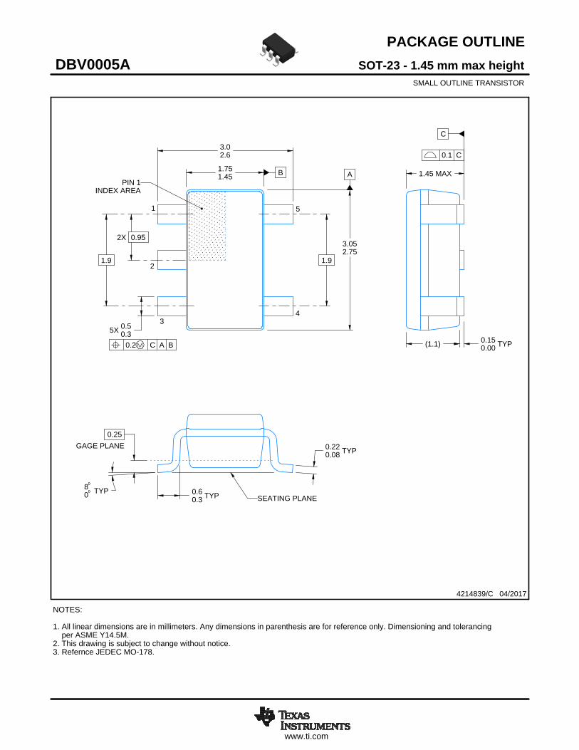
PACKAGE OUTLINE
C
TYP0.220.08
0.25
3.02.6
2X 0.95
1.9
1.45 MAX
TYP0.150.00
5X 0.50.3
TYP0.60.3
TYP80
1.9
A
3.052.75
B1.751.45
(1.1)
SOT-23 - 1.45 mm max heightDBV0005ASMALL OUTLINE TRANSISTOR
4214839/C 04/2017
NOTES: 1. All linear dimensions are in millimeters. Any dimensions in parenthesis are for reference only. Dimensioning and tolerancing per ASME Y14.5M.2. This drawing is subject to change without notice.3. Refernce JEDEC MO-178.
0.2 C A B
1
34
5
2
INDEX AREAPIN 1
GAGE PLANE
SEATING PLANE
0.1 C
SCALE 4.000
www.ti.com
EXAMPLE BOARD LAYOUT
0.07 MAXARROUND
0.07 MINARROUND
5X (1.1)
5X (0.6)
(2.6)
(1.9)
2X (0.95)
(R0.05) TYP
4214839/C 04/2017
SOT-23 - 1.45 mm max heightDBV0005ASMALL OUTLINE TRANSISTOR
NOTES: (continued) 4. Publication IPC-7351 may have alternate designs. 5. Solder mask tolerances between and around signal pads can vary based on board fabrication site.
SYMM
LAND PATTERN EXAMPLEEXPOSED METAL SHOWN
SCALE:15X
PKG
1
3 4
5
2
SOLDER MASKOPENINGMETAL UNDER
SOLDER MASK
SOLDER MASKDEFINED
EXPOSED METAL
METALSOLDER MASKOPENING
NON SOLDER MASKDEFINED
(PREFERRED)
SOLDER MASK DETAILS
EXPOSED METAL

www.ti.com
EXAMPLE STENCIL DESIGN
(2.6)
(1.9)
2X(0.95)
5X (1.1)
5X (0.6)
(R0.05) TYP
SOT-23 - 1.45 mm max heightDBV0005ASMALL OUTLINE TRANSISTOR
4214839/C 04/2017
NOTES: (continued) 6. Laser cutting apertures with trapezoidal walls and rounded corners may offer better paste release. IPC-7525 may have alternate design recommendations. 7. Board assembly site may have different recommendations for stencil design.
SOLDER PASTE EXAMPLEBASED ON 0.125 mm THICK STENCIL
SCALE:15X
SYMM
PKG
1
3 4
5
2

www.ti.com
PACKAGE OUTLINE
C
TYP0.220.08
0.25
3.02.6
2X 0.95
1.9
1.45 MAX
TYP0.150.00
5X 0.50.3
TYP0.60.3
TYP80
1.9
A
3.052.75
B1.751.45
(1.1)
SOT-23 - 1.45 mm max heightDBV0005ASMALL OUTLINE TRANSISTOR
4214839/C 04/2017
NOTES: 1. All linear dimensions are in millimeters. Any dimensions in parenthesis are for reference only. Dimensioning and tolerancing per ASME Y14.5M.2. This drawing is subject to change without notice.3. Refernce JEDEC MO-178.
0.2 C A B
1
34
5
2
INDEX AREAPIN 1
GAGE PLANE
SEATING PLANE
0.1 C
SCALE 4.000

www.ti.com
EXAMPLE BOARD LAYOUT
0.07 MAXARROUND
0.07 MINARROUND
5X (1.1)
5X (0.6)
(2.6)
(1.9)
2X (0.95)
(R0.05) TYP
4214839/C 04/2017
SOT-23 - 1.45 mm max heightDBV0005ASMALL OUTLINE TRANSISTOR
NOTES: (continued) 4. Publication IPC-7351 may have alternate designs. 5. Solder mask tolerances between and around signal pads can vary based on board fabrication site.
SYMM
LAND PATTERN EXAMPLEEXPOSED METAL SHOWN
SCALE:15X
PKG
1
3 4
5
2
SOLDER MASKOPENINGMETAL UNDER
SOLDER MASK
SOLDER MASKDEFINED
EXPOSED METAL
METALSOLDER MASKOPENING
NON SOLDER MASKDEFINED
(PREFERRED)
SOLDER MASK DETAILS
EXPOSED METAL

www.ti.com
EXAMPLE STENCIL DESIGN
(2.6)
(1.9)
2X(0.95)
5X (1.1)
5X (0.6)
(R0.05) TYP
SOT-23 - 1.45 mm max heightDBV0005ASMALL OUTLINE TRANSISTOR
4214839/C 04/2017
NOTES: (continued) 6. Laser cutting apertures with trapezoidal walls and rounded corners may offer better paste release. IPC-7525 may have alternate design recommendations. 7. Board assembly site may have different recommendations for stencil design.
SOLDER PASTE EXAMPLEBASED ON 0.125 mm THICK STENCIL
SCALE:15X
SYMM
PKG
1
3 4
5
2

GENERIC PACKAGE VIEW
Images above are just a representation of the package family, actual package may vary.Refer to the product data sheet for package details.
DRV 6 WSON - 0.8 mm max heightPLASTIC SMALL OUTLINE - NO LEAD
4206925/F

www.ti.com
PACKAGE OUTLINE
C
6X 0.350.25
1.6 0.1
6X 0.30.2
2X1.3
1 0.1
4X 0.65
0.80.7
0.050.00
B 2.11.9
A
2.11.9
(0.2) TYP
WSON - 0.8 mm max heightDRV0006APLASTIC SMALL OUTLINE - NO LEAD
4222173/B 04/2018
PIN 1 INDEX AREA
SEATING PLANE
0.08 C
1
34
6
(OPTIONAL)PIN 1 ID
0.1 C A B0.05 C
THERMAL PADEXPOSED
7
NOTES: 1. All linear dimensions are in millimeters. Any dimensions in parenthesis are for reference only. Dimensioning and tolerancing per ASME Y14.5M. 2. This drawing is subject to change without notice. 3. The package thermal pad must be soldered to the printed circuit board for thermal and mechanical performance.
SCALE 5.500
www.ti.com
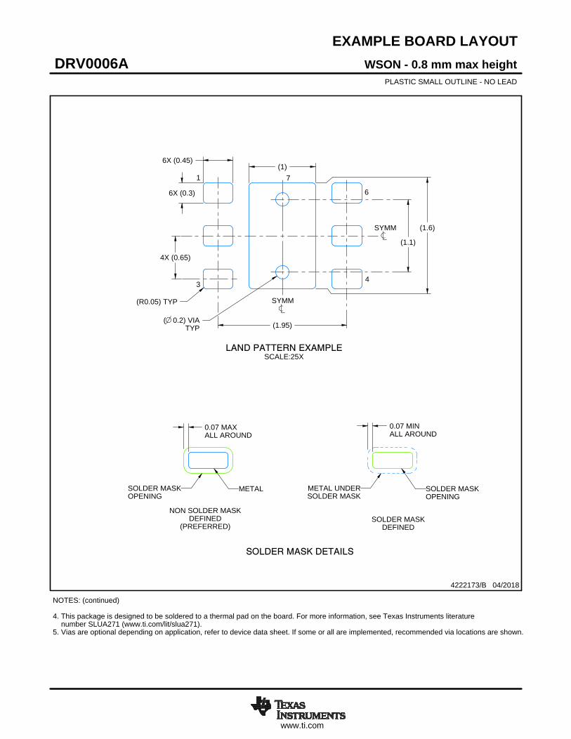
EXAMPLE BOARD LAYOUT
0.07 MINALL AROUND
0.07 MAXALL AROUND
(1)
4X (0.65)
(1.95)
6X (0.3)
6X (0.45)
(1.6)
(R0.05) TYP
( 0.2) VIATYP
(1.1)
WSON - 0.8 mm max heightDRV0006APLASTIC SMALL OUTLINE - NO LEAD
4222173/B 04/2018
SYMM
1
34
6
SYMM
LAND PATTERN EXAMPLESCALE:25X
7
NOTES: (continued) 4. This package is designed to be soldered to a thermal pad on the board. For more information, see Texas Instruments literature number SLUA271 (www.ti.com/lit/slua271).5. Vias are optional depending on application, refer to device data sheet. If some or all are implemented, recommended via locations are shown.
SOLDER MASKOPENINGSOLDER MASK
METAL UNDER
SOLDER MASKDEFINED
METALSOLDER MASKOPENING
SOLDER MASK DETAILS
NON SOLDER MASKDEFINED
(PREFERRED)

www.ti.com
EXAMPLE STENCIL DESIGN
6X (0.3)
6X (0.45)
4X (0.65)
(0.7)
(1)
(1.95)
(R0.05) TYP
(0.45)
WSON - 0.8 mm max heightDRV0006APLASTIC SMALL OUTLINE - NO LEAD
4222173/B 04/2018
NOTES: (continued) 6. Laser cutting apertures with trapezoidal walls and rounded corners may offer better paste release. IPC-7525 may have alternate design recommendations.
SOLDER PASTE EXAMPLEBASED ON 0.125 mm THICK STENCIL
EXPOSED PAD #7
88% PRINTED SOLDER COVERAGE BY AREA UNDER PACKAGESCALE:30X
SYMM
1
3 4
6
SYMM
METAL7

IMPORTANT NOTICE
Texas Instruments Incorporated (TI) reserves the right to make corrections, enhancements, improvements and other changes to itssemiconductor products and services per JESD46, latest issue, and to discontinue any product or service per JESD48, latest issue. Buyersshould obtain the latest relevant information before placing orders and should verify that such information is current and complete.TI’s published terms of sale for semiconductor products (http://www.ti.com/sc/docs/stdterms.htm) apply to the sale of packaged integratedcircuit products that TI has qualified and released to market. Additional terms may apply to the use or sale of other types of TI products andservices.Reproduction of significant portions of TI information in TI data sheets is permissible only if reproduction is without alteration and isaccompanied by all associated warranties, conditions, limitations, and notices. TI is not responsible or liable for such reproduceddocumentation. Information of third parties may be subject to additional restrictions. Resale of TI products or services with statementsdifferent from or beyond the parameters stated by TI for that product or service voids all express and any implied warranties for theassociated TI product or service and is an unfair and deceptive business practice. TI is not responsible or liable for any such statements.Buyers and others who are developing systems that incorporate TI products (collectively, “Designers”) understand and agree that Designersremain responsible for using their independent analysis, evaluation and judgment in designing their applications and that Designers havefull and exclusive responsibility to assure the safety of Designers' applications and compliance of their applications (and of all TI productsused in or for Designers’ applications) with all applicable regulations, laws and other applicable requirements. Designer represents that, withrespect to their applications, Designer has all the necessary expertise to create and implement safeguards that (1) anticipate dangerousconsequences of failures, (2) monitor failures and their consequences, and (3) lessen the likelihood of failures that might cause harm andtake appropriate actions. Designer agrees that prior to using or distributing any applications that include TI products, Designer willthoroughly test such applications and the functionality of such TI products as used in such applications.TI’s provision of technical, application or other design advice, quality characterization, reliability data or other services or information,including, but not limited to, reference designs and materials relating to evaluation modules, (collectively, “TI Resources”) are intended toassist designers who are developing applications that incorporate TI products; by downloading, accessing or using TI Resources in anyway, Designer (individually or, if Designer is acting on behalf of a company, Designer’s company) agrees to use any particular TI Resourcesolely for this purpose and subject to the terms of this Notice.TI’s provision of TI Resources does not expand or otherwise alter TI’s applicable published warranties or warranty disclaimers for TIproducts, and no additional obligations or liabilities arise from TI providing such TI Resources. TI reserves the right to make corrections,enhancements, improvements and other changes to its TI Resources. TI has not conducted any testing other than that specificallydescribed in the published documentation for a particular TI Resource.Designer is authorized to use, copy and modify any individual TI Resource only in connection with the development of applications thatinclude the TI product(s) identified in such TI Resource. NO OTHER LICENSE, EXPRESS OR IMPLIED, BY ESTOPPEL OR OTHERWISETO ANY OTHER TI INTELLECTUAL PROPERTY RIGHT, AND NO LICENSE TO ANY TECHNOLOGY OR INTELLECTUAL PROPERTYRIGHT OF TI OR ANY THIRD PARTY IS GRANTED HEREIN, including but not limited to any patent right, copyright, mask work right, orother intellectual property right relating to any combination, machine, or process in which TI products or services are used. Informationregarding or referencing third-party products or services does not constitute a license to use such products or services, or a warranty orendorsement thereof. Use of TI Resources may require a license from a third party under the patents or other intellectual property of thethird party, or a license from TI under the patents or other intellectual property of TI.TI RESOURCES ARE PROVIDED “AS IS” AND WITH ALL FAULTS. TI DISCLAIMS ALL OTHER WARRANTIES ORREPRESENTATIONS, EXPRESS OR IMPLIED, REGARDING RESOURCES OR USE THEREOF, INCLUDING BUT NOT LIMITED TOACCURACY OR COMPLETENESS, TITLE, ANY EPIDEMIC FAILURE WARRANTY AND ANY IMPLIED WARRANTIES OFMERCHANTABILITY, FITNESS FOR A PARTICULAR PURPOSE, AND NON-INFRINGEMENT OF ANY THIRD PARTY INTELLECTUALPROPERTY RIGHTS. TI SHALL NOT BE LIABLE FOR AND SHALL NOT DEFEND OR INDEMNIFY DESIGNER AGAINST ANY CLAIM,INCLUDING BUT NOT LIMITED TO ANY INFRINGEMENT CLAIM THAT RELATES TO OR IS BASED ON ANY COMBINATION OFPRODUCTS EVEN IF DESCRIBED IN TI RESOURCES OR OTHERWISE. IN NO EVENT SHALL TI BE LIABLE FOR ANY ACTUAL,DIRECT, SPECIAL, COLLATERAL, INDIRECT, PUNITIVE, INCIDENTAL, CONSEQUENTIAL OR EXEMPLARY DAMAGES INCONNECTION WITH OR ARISING OUT OF TI RESOURCES OR USE THEREOF, AND REGARDLESS OF WHETHER TI HAS BEENADVISED OF THE POSSIBILITY OF SUCH DAMAGES.Unless TI has explicitly designated an individual product as meeting the requirements of a particular industry standard (e.g., ISO/TS 16949and ISO 26262), TI is not responsible for any failure to meet such industry standard requirements.Where TI specifically promotes products as facilitating functional safety or as compliant with industry functional safety standards, suchproducts are intended to help enable customers to design and create their own applications that meet applicable functional safety standardsand requirements. Using products in an application does not by itself establish any safety features in the application. Designers mustensure compliance with safety-related requirements and standards applicable to their applications. Designer may not use any TI products inlife-critical medical equipment unless authorized officers of the parties have executed a special contract specifically governing such use.Life-critical medical equipment is medical equipment where failure of such equipment would cause serious bodily injury or death (e.g., lifesupport, pacemakers, defibrillators, heart pumps, neurostimulators, and implantables). Such equipment includes, without limitation, allmedical devices identified by the U.S. Food and Drug Administration as Class III devices and equivalent classifications outside the U.S.TI may expressly designate certain products as completing a particular qualification (e.g., Q100, Military Grade, or Enhanced Product).Designers agree that it has the necessary expertise to select the product with the appropriate qualification designation for their applicationsand that proper product selection is at Designers’ own risk. Designers are solely responsible for compliance with all legal and regulatoryrequirements in connection with such selection.Designer will fully indemnify TI and its representatives against any damages, costs, losses, and/or liabilities arising out of Designer’s non-compliance with the terms and provisions of this Notice.
Mailing Address: Texas Instruments, Post Office Box 655303, Dallas, Texas 75265Copyright © 2018, Texas Instruments Incorporated