Embed Size (px)
Citation preview
TL16C554A, TL16C554AIASYNCHRONOUS-COMMUNICATIONS ELEMENT
�
�
SLLS509E − AUGUST 2001 − REVISED JUNE 2010
1POST OFFICE BOX 655303 • DALLAS, TEXAS 75265
� Integrated Asynchronous-CommunicationsElement
� Consists of Four Improved TL16C550CACEs Plus Steering Logic
� In FIFO Mode, Each ACE Transmitter andReceiver Is Buffered With 16-Byte FIFO toReduce the Number of Interrupts to CPU
� In TL16C450 Mode, Hold and ShiftRegisters Eliminate Need for PreciseSynchronization Between the CPU andSerial Data
� Up to 16-MHz Clock Rate for up to 1-MbaudOperation with VCC = 3.3 V and 5 V
� Programmable Baud-Rate GeneratorsWhich Allow Division of Any InputReference Clock by 1 to (216�−�1) andGenerate an Internal 16 × Clock
� Adds or Deletes Standard AsynchronousCommunication Bits (Start, Stop, andParity) to or From the Serial-Data Stream
� Independently Controlled Transmit,Receive, Line Status, and Data SetInterrupts
� 5-V and 3.3-V Operation
� Fully Programmable Serial InterfaceCharacteristics:− 5-, 6-, 7-, or 8-Bit Characters− Even-, Odd-, or No-Parity Bit− 1-, 1 1/2-, or 2-Stop Bit Generation− Baud Generation (DC to 1-Mbit Per
Second)
� False Start Bit Detection
� Complete Status Reporting Capabilities
� Line Break Generation and Detection
� Internal Diagnostic Capabilities:− Loopback Controls for Communications
Link Fault Isolation− Break, Parity, Overrun, Framing Error
Simulation
� Fully Prioritized Interrupt System Controls
� Modem Control Functions (CTS, RTS, DSR,DTR, RI, and DCD)
� 3-State Outputs Provide TTL DriveCapabilities for Bidirectional Data Bus andControl Bus
� Programmable Auto-RTS and Auto-CTS
� CTS Controls Transmitter in Auto-CTSMode,
� RCV FIFO Contents and Threshold ControlRTS in Auto-RTS Mode,
description
The TL16C554A is an enhanced quadruple version of the TL16C550C asynchronous-communications element(ACE). Each channel performs serial-to-parallel conversion on data characters received from peripheraldevices or modems and parallel-to-serial conversion on data characters transmitted by the CPU. The completestatus of each channel of the quadruple ACE can be read by the CPU at any time during operation. Theinformation obtained includes the type and condition of the operation performed and any error conditionsencountered.
The TL16C554A quadruple ACE can be placed in an alternate FIFO mode, which activates the internal FIFOsto allow 16 bytes (plus three bits of error data per byte in the receiver FIFO) to be stored in both receive andtransmit modes. In the FIFO mode of operation, there is a selectable autoflow control feature that cansignificantly reduce software overhead and increase system efficiency by automatically controlling serial-dataflow using RTS output and CTS input signals. All logic is on the chip to minimize system overhead and maximizesystem efficiency. Two terminal functions allow signaling of direct-memory access (DMA) transfers. Each ACEincludes a programmable baud-rate generator that can divide the timing reference clock input by a divisorbetween 1 and 216−1.
The TL16C554A is available in a 68-pin plastic-leaded chip-carrier (PLCC) FN package, 64-pin plastic quadflatpack (PQFP) PM package and in an 80-pin (TQFP) PN package.
Please be aware that an important notice concerning availability, standard warranty, and use in critical applications ofTexas Instruments semiconductor products and disclaimers thereto appears at the end of this data sheet.
�
PRODUCTION DATA information is current as of publication date.Products conform to specifications per the terms of Texas Instrumentsstandard warranty. Production processing does not necessarily includetesting of all parameters.
Copyright © 2010, Texas Instruments Incorporated
TL16C554A, TL16C554AIASYNCHRONOUS-COMMUNICATIONS ELEMENT�
�
SLLS509E − AUGUST 2001 − REVISED JUNE 2010
2 POST OFFICE BOX 655303 • DALLAS, TEXAS 75265
28 29
DSRDCTSDDTRDGNDRTSDINTDCSDTXDIORTXCCSCINTCRTSCVCC
DTRCCTSCDSRC
60
59
58
57
56
55
54
53
52
51
50
49
48
47
46
45
4430
10
11
12
13
14
15
16
17
18
19
20
21
22
23
24
25
26
DSRACTSADTRA
VCC
RTSAINTACSATXAIOWTXBCSBINTB
RTSBGND
DTRBCTSBDSRB
31 32 33 34
FN PACKAGE(TOP VIEW)
D2
D1
8 7 6 5 49 3
RX
AG
ND
D7
D6
D5
D4
D3
XTA
L2R
ES
ET
RX
RD
YT
XR
DY
RX
B
NC A2
A1
A0
XTA
L1
1 68 672
35 36 37 38 39
66 65
27
DC
DB
D0
INT
N
64 63 62 61
40 41 42 43G
ND
RX
CR
ICD
CD
C
RX
DR
IDD
CD
D
DC
DA
RIA
VC
C
RIB
VC
C
NC − No internal connection
TL16C554A, TL16C554AIASYNCHRONOUS-COMMUNICATIONS ELEMENT
�
�
SLLS509E − AUGUST 2001 − REVISED JUNE 2010
3POST OFFICE BOX 655303 • DALLAS, TEXAS 75265
2 3
DSRCDCDCRICRXCGNDRESETXTAL2XTAL1A0A1A2VCC
RXBRIBDCDBDSRB
32
31
30
29
28
27
26
25
24
23
22
21
20
19
18
174
49
50
51
52
53
54
55
56
57
58
59
60
61
62
63
64
DCDDRID
RXDVCC
D0D1D2D3D4D5D6D7
GNDRXARIA
DCDA5 6 7 8
PM PACKAGE(TOP VIEW)
TX
CC
SC
47 46 45 44 4348 42
DT
RD
GN
DR
TS
DIN
TD
CS
DT
XD
IOR
TX
BC
SB
INT
BR
TS
B
DT
RA
RT
SA
INTA
CS
AT
XA
IOW
40 39 3841
9 10 11 12 13
37 36
1
DS
RA
INT
CR
TS
C
35 34 33
14 15 16
GN
DD
TR
BC
TS
BD
TR
CC
TS
C
DS
RD
CT
SD
VC
C
CT
SA
VC
C
NC − No internal connection
TL16C554A, TL16C554AIASYNCHRONOUS-COMMUNICATIONS ELEMENT�
�
SLLS509E − AUGUST 2001 − REVISED JUNE 2010
4 POST OFFICE BOX 655303 • DALLAS, TEXAS 75265
2 3
NCDSRBCTSBDTRBGNDRTSBINTBCSBTXBIOWNCTXACSAINTARTSAVCC
DTRACTSADSRANC
40
39
38
37
36
35
34
33
32
31
30
29
28
27
26
25
24
23
22
214
61
62
63
64
65
66
67
68
69
70
71
72
73
74
75
76
77
78
79
80
NCDSRCCTSCDTRC
VCCRTSCINTCCSCTXCIORNC
TXDCSDINTD
RTSDGND
DTRDCTSDDSRD
NC5 6 7 8
PN PACKAGE(TOP VIEW)
XTA
L1
59 58 57 56 5560 54
RIC
RX
CG
ND
TX
RD
YR
XR
DY
RE
SE
TN
C
D3
D5
RID
RX
D
NC
INT
N D0
D1
D2
52 51 5053
9 10 11 12 13
49 48
1
NC
A0
47 46 45 44
14 15 16 17
D6
D7
GN
DR
XA
A1
A2
XTA
L2
RX
B
NC
DC
DC
RIA
DC
DA
18 19 20
RIB
DC
DB
43 42 41
VC
C
NC
NC
CC
V
DC
DD D4
NC
NC − No internal connection
TL16C554A, TL16C554AIASYNCHRONOUS-COMMUNICATIONS ELEMENT
�
�
SLLS509E − AUGUST 2001 − REVISED JUNE 2010
5POST OFFICE BOX 655303 • DALLAS, TEXAS 75265
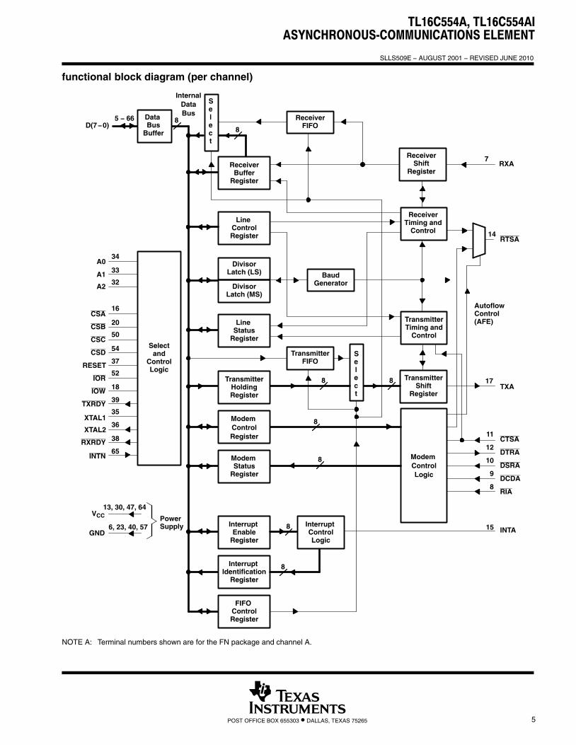
functional block diagram (per channel)
ReceiverBuffer
Register
DivisorLatch (LS)
DivisorLatch (MS)
BaudGenerator
ReceiverFIFO
Line Status
Register
TransmitterHoldingRegister
Modem ControlRegister
Modem Status
Register
Line ControlRegister
TransmitterFIFO
Interrupt Enable
Register
Interrupt Identification
Register
FIFO ControlRegister
Selectand
ControlLogic
Interrupt ControlLogic
Select
Data Bus
Buffer
RXA
TXA
CTSA
DTRA
DSRA
DCDA
RIA
INTA
11
12
10
9
8
15
17
7
16
A034
D(7−0)5 − 66
InternalDataBus
33
32
20
50
54
37
52
18
39
35
36
38
65
A1
A2
CSA
CSB
CSC
CSD
RESET
IOR
IOW
XTAL1
RXRDY
Select
ReceiverShift
Register
ReceiverTiming and
Control
TransmitterTiming and
Control
TransmitterShift
Register
Modem ControlLogic
8
13, 30, 47, 64
6, 23, 40, 57
VCC
GND
PowerSupply
RTSA14
AutoflowControl(AFE)
8
8
8
8
8
8
8
TXRDY
XTAL2
INTN
NOTE A: Terminal numbers shown are for the FN package and channel A.
TL16C554A, TL16C554AIASYNCHRONOUS-COMMUNICATIONS ELEMENT�
�
SLLS509E − AUGUST 2001 − REVISED JUNE 2010
6 POST OFFICE BOX 655303 • DALLAS, TEXAS 75265
Terminal Functions
TERMINAL
NAMEFNNO.
PMNO.
PNNO.
I/O DESCRIPTION
A0A1A2
343332
22,23,24
484746
I Register select terminals. A0, A1, and A2 are three inputs used during read and writeoperations to select the ACE register to read or write.
CSA, CSB,CSC, CSD
16, 20,50, 54
7, 11,38, 42
28, 33,68, 73
I Chip select. Each chip select (CSx) enables read and write operations to its respectivechannel.
CTSA, CTSB,CTSC, CTSD
11, 25,45, 59
2, 16,33, 47
23, 38,63, 78
I Clear to send. CTS is a modem status signal. Its condition can be checked by reading bit4 (CTS) of the modem-status register. Bit 0 (ΔCTS) of the modem-status register indicatesthat CTS has changed state since the last read from the modem-status register. If themodem-status interrupt is enabled when CTS changes levels and the auto-CTS mode isnot enabled, an interrupt is generated. CTS is also used in the auto-CTS mode to controlthe transmitter.
D7−D0 66−681−5
53−60 15−11,9−7
I/O Data bus. Eight data lines with 3-state outputs provide a bidirectional path for data, control,and status information between the TL16C554A and the CPU. D0 is the least-significantbit (LSB).
DCDA, DCDB,DCDC, DCDD
9, 27,43, 61
18, 31,49, 64
19,42,59, 2
I Data carrier detect. A low on DCDx indicates the carrier has been detected by the modem.The condition of this signal is checked by reading bit 7 of the modem-status register.
DSRA, DSRB,DSRC, DSRD
10, 26,44, 60
1, 17,32, 48
22, 39,62, 79
I Data set ready. DSRx is a modem-status signal. Its condition can be checked by readingbit 5 (DSR) of the modem-status register. DSR has no effect on the transmit or receiveoperation.
DTRA, DTRB,DTRC, DTRD
12, 24,46, 58
3, 15,34, 46
24, 37,64, 77
O Data terminal ready. DTRx is an output that indicates to a modem or data set that the ACEis ready to establish communications. It is placed in the active state by setting the DTR bitof the modem-control register. DTRx is placed in the inactive state (high) either as a result of the masterreset during loop-mode operation, or when clearing bit 0 (DTR) of the modem-controlregister.
GND 6, 23,40, 57
14,28, 45,
61
16, 36,56, 76
Signal and power ground
INTN 65 6 I Interrupt normal. INTN operates in conjunction with bit 3 of the modem-status register andaffects operation of the interrupts (INTA, INTB, INTC, and INTD) for the four universalasynchronous receiver/transceivers (UARTs) per the following table.
INTN OPERATION OF INTERRUPTS
Brought low orallowed to float
Interrupts are enabled according to the state of OUT2 (MCR bit 3). Whenthe MCR bit 3 is cleared, the 3-state interrupt output of that UART is inthe high-impedance state. When the MCR bit 3 is set, the interrupt outputof the UART is enabled.
Brought high Interrupts are always enabled, overriding the OUT2 enables.
INTA, INTB,INTC, INTD
15, 21,49, 55
6, 12,37, 43
27, 34,67, 74
O External interrupt output. The INTx outputs go high (when enabled by the interrupt register)and inform the CPU that the ACE has an interrupt to be serviced. Four conditions that causean interrupt to be issued are: receiver error, receiver data available or timeout (FIFO modeonly), transmitter holding register empty, and an enabled modem-status interrupt. Theinterrupt is disabled when it is serviced or as the result of a master reset.
IOR 52 40 70 I Read strobe. A low level on IOR transfers the contents of the selected register to theexternal CPU bus.
IOW 18 9 31 I Write strobe. IOW allows the the CPU to write to the register selected by the address.
RESET 37 27 53 I Master reset. When active, RESET clears most ACE registers and sets the state of varioussignals. The transmitter output and the receiver input are disabled during reset time.
TL16C554A, TL16C554AIASYNCHRONOUS-COMMUNICATIONS ELEMENT
�
�
SLLS509E − AUGUST 2001 − REVISED JUNE 2010
7POST OFFICE BOX 655303 • DALLAS, TEXAS 75265
Terminal Functions (Continued)
TERMINAL
NAMEFNNO.
PMNO.
PNNO.
I/O DESCRIPTION
RIA, RIB,RIC, RID
19, 30,50, 63
18, 43,58, 3
I Ring detect indicator. A low on RIx indicates the modem has received a ring signal fromthe telephone line. The condition of this signal can be checked by reading bit 6 of themodem-status register.
RTSA, RTSB,RTSC, RTSD
5, 13,36, 44
26, 35,66, 75
O Request to send. When active, RTS informs the modem or data set that the ACE is readyto receive data. RTS is set to the active level by setting the RTS modem-control registerbit, and is set to the inactive (high) level either as a result of a master reset, or duringloop-mode operations, or by clearing bit 1 (RTS) of the MCR. In the auto-RTS mode, RTSis set to the inactive level by the receiver threshold-control logic.
RXA, RXBRXC, RXD
7, 29,41, 63
20, 29,51, 62
17, 44,57, 4
I Serial input. RXx is a serial-data input from a connected communications device. Duringloopback mode, the RXx input is disabled from external connection and connected to theTXx output internally.
RXRDY 38 54 O Receive ready. RXRDY goes low when the receive FIFO is full. It can be used as a singletransfer or multitransfer.
TXA, TXBTXC, TXD
17, 19,51, 53
8, 10,39, 41
29, 32,69, 72
O Transmit outputs. TXx is a composite serial-data output connected to a communicationsdevice. TXA, TXB, TXC, and TXD are set to the marking (high) state as a result of reset.
TXRDY 39 55 O Transmit ready. TXRDY goes low when the transmit FIFO is full. It can be used as a singletransfer or multitransfer function.
VCC 13, 30,47, 64
21, 35,52
5, 25,45, 65
Power supply
XTAL1 35 25 50 I Crystal input 1 or external clock input. A crystal can be connected to XTAL1 and XTAL2 toutilize the internal oscillator circuit. An external clock can be connected to drive theinternal-clock circuits.
XTAL2 36 26 51 O Crystal output 2 or buffered clock output (see XTAL1).
absolute maximum ratings over free-air temperature range (unless otherwise noted)†
Supply voltage range, VCC (see Note 1) −0.5 V to 7 V. . . . . . . . . . . . . . . . . . . . . . . . . . . . . . . . . . . . . . . . . . . . . . . Input voltage range at any input, VI −0.5 V to 7 V. . . . . . . . . . . . . . . . . . . . . . . . . . . . . . . . . . . . . . . . . . . . . . . . . . . Output voltage range, VO −0.5 V to VCC + 3 V. . . . . . . . . . . . . . . . . . . . . . . . . . . . . . . . . . . . . . . . . . . . . . . . . . . . . Continuous total-power dissipation at (or below) 70°C 500 mW. . . . . . . . . . . . . . . . . . . . . . . . . . . . . . . . . . . . . . . Operating free-air temperature range, TA: TL16C554A 0°C to 70°C. . . . . . . . . . . . . . . . . . . . . . . . . . . . . . . . . .
TL16C554AI −40°C to 85°C. . . . . . . . . . . . . . . . . . . . . . . . . . . . . . . Storage temperature range, Tstg −65°C to 150°C. . . . . . . . . . . . . . . . . . . . . . . . . . . . . . . . . . . . . . . . . . . . . . . . . . .
† Stresses beyond those listed under “absolute maximum ratings” may cause permanent damage to the device. These are stress ratings only, andfunctional operation of the device at these or any other conditions beyond those indicated under “recommended operating conditions” is notimplied. Exposure to absolute-maximum-rated conditions for extended periods may affect device reliability.
NOTE 1: All voltage levels are with respect to GND.
TL16C554A, TL16C554AIASYNCHRONOUS-COMMUNICATIONS ELEMENT�
�
SLLS509E − AUGUST 2001 − REVISED JUNE 2010
8 POST OFFICE BOX 655303 • DALLAS, TEXAS 75265
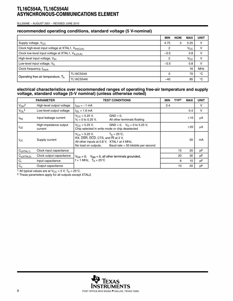
recommended operating conditions, standard voltage (5 V-nominal)
MIN NOM MAX UNIT
Supply voltage, VCC 4.75 5 5.25 V
Clock high-level input voltage at XTAL1, VIH(CLK) 2 VCC V
Clock low-level input voltage at XTAL1, VIL(CLK) −0.5 0.8 V
High-level input voltage, VIH 2 VCC V
Low-level input voltage, VIL −0.5 0.8 V
Clock frequency, fclock 16 MHz
Operating free air temperature TTL16C554A 0 70 °C
Operating free-air temperature, TATL16C554AI −40 85 °C
electrical characteristics over recommended ranges of operating free-air temperature and supplyvoltage, standard voltage (5-V nominal) (unless otherwise noted)
PARAMETER TEST CONDITIONS MIN TYP† MAX UNIT
VOH‡ High-level output voltage IOH = −1 mA 2.4 V
VOL‡ Low-level output voltage IOL = 1.6 mA 0.4 V
IIkg Input leakage currentVCC = 5.25 V, GND = 0,VI = 0 to 5.25 V, All other terminals floating
±10 μA
IOZHigh-impedance output current
VCC = 5.25 V, GND = 0, VO = 0 to 5.25 V,Chip selected in write mode or chip deselected
±20 μA
ICC Supply current
VCC = 5.25 V, TA = 25°C,RX, DSR, DCD, CTS, and RI at 2 V,All other inputs at 0.8 V, XTAL1 at 4 MHz,No load on outputs, Baud rate = 50 kilobits per second
50 mA
Ci(XTAL1) Clock input capacitance 15 20 pF
Co(XTAL2) Clock output capacitance VCC = 0, VSS = 0, all other terminals grounded, 20 30 pF
Ci Input capacitance
VCC = 0, VSS = 0, all other terminals grounded,f = 1 MHz, TA = 25°C 6 10 pF
Co Output capacitance 10 20 pF† All typical values are at VCC = 5 V, TA = 25°C.‡ These parameters apply for all outputs except XTAL2.
TL16C554A, TL16C554AIASYNCHRONOUS-COMMUNICATIONS ELEMENT
�
�
SLLS509E − AUGUST 2001 − REVISED JUNE 2010
9POST OFFICE BOX 655303 • DALLAS, TEXAS 75265
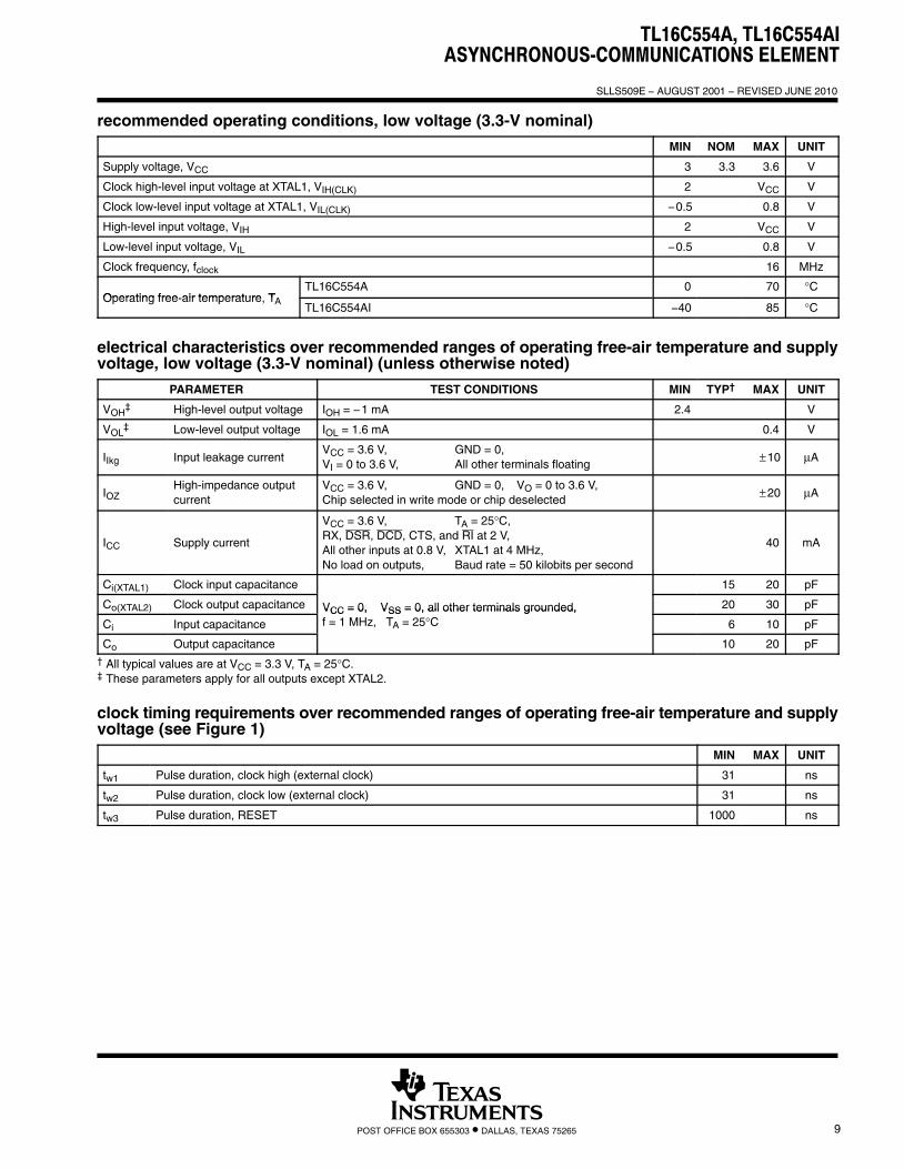
recommended operating conditions, low voltage (3.3-V nominal)
MIN NOM MAX UNIT
Supply voltage, VCC 3 3.3 3.6 V
Clock high-level input voltage at XTAL1, VIH(CLK) 2 VCC V
Clock low-level input voltage at XTAL1, VIL(CLK) −0.5 0.8 V
High-level input voltage, VIH 2 VCC V
Low-level input voltage, VIL −0.5 0.8 V
Clock frequency, fclock 16 MHz
Operating free air temperature TTL16C554A 0 70 °C
Operating free-air temperature, TATL16C554AI −40 85 °C
electrical characteristics over recommended ranges of operating free-air temperature and supplyvoltage, low voltage (3.3-V nominal) (unless otherwise noted)
PARAMETER TEST CONDITIONS MIN TYP† MAX UNIT
VOH‡ High-level output voltage IOH = −1 mA 2.4 V
VOL‡ Low-level output voltage IOL = 1.6 mA 0.4 V
IIkg Input leakage currentVCC = 3.6 V, GND = 0,VI = 0 to 3.6 V, All other terminals floating
±10 μA
IOZHigh-impedance output current
VCC = 3.6 V, GND = 0, VO = 0 to 3.6 V,Chip selected in write mode or chip deselected
±20 μA
ICC Supply current
VCC = 3.6 V, TA = 25°C,RX, DSR, DCD, CTS, and RI at 2 V,All other inputs at 0.8 V, XTAL1 at 4 MHz,No load on outputs, Baud rate = 50 kilobits per second
40 mA
Ci(XTAL1) Clock input capacitance 15 20 pF
Co(XTAL2) Clock output capacitance VCC = 0, VSS = 0, all other terminals grounded, 20 30 pF
Ci Input capacitance
VCC = 0, VSS = 0, all other terminals grounded,f = 1 MHz, TA = 25°C 6 10 pF
Co Output capacitance 10 20 pF† All typical values are at VCC = 3.3 V, TA = 25°C.‡ These parameters apply for all outputs except XTAL2.
clock timing requirements over recommended ranges of operating free-air temperature and supplyvoltage (see Figure 1)
MIN MAX UNIT
tw1 Pulse duration, clock high (external clock) 31 ns
tw2 Pulse duration, clock low (external clock) 31 ns
tw3 Pulse duration, RESET 1000 ns
TL16C554A, TL16C554AIASYNCHRONOUS-COMMUNICATIONS ELEMENT�
�
SLLS509E − AUGUST 2001 − REVISED JUNE 2010
10 POST OFFICE BOX 655303 • DALLAS, TEXAS 75265
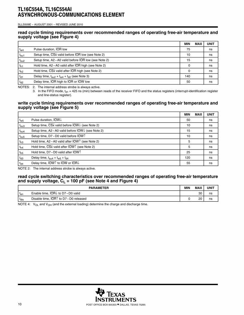
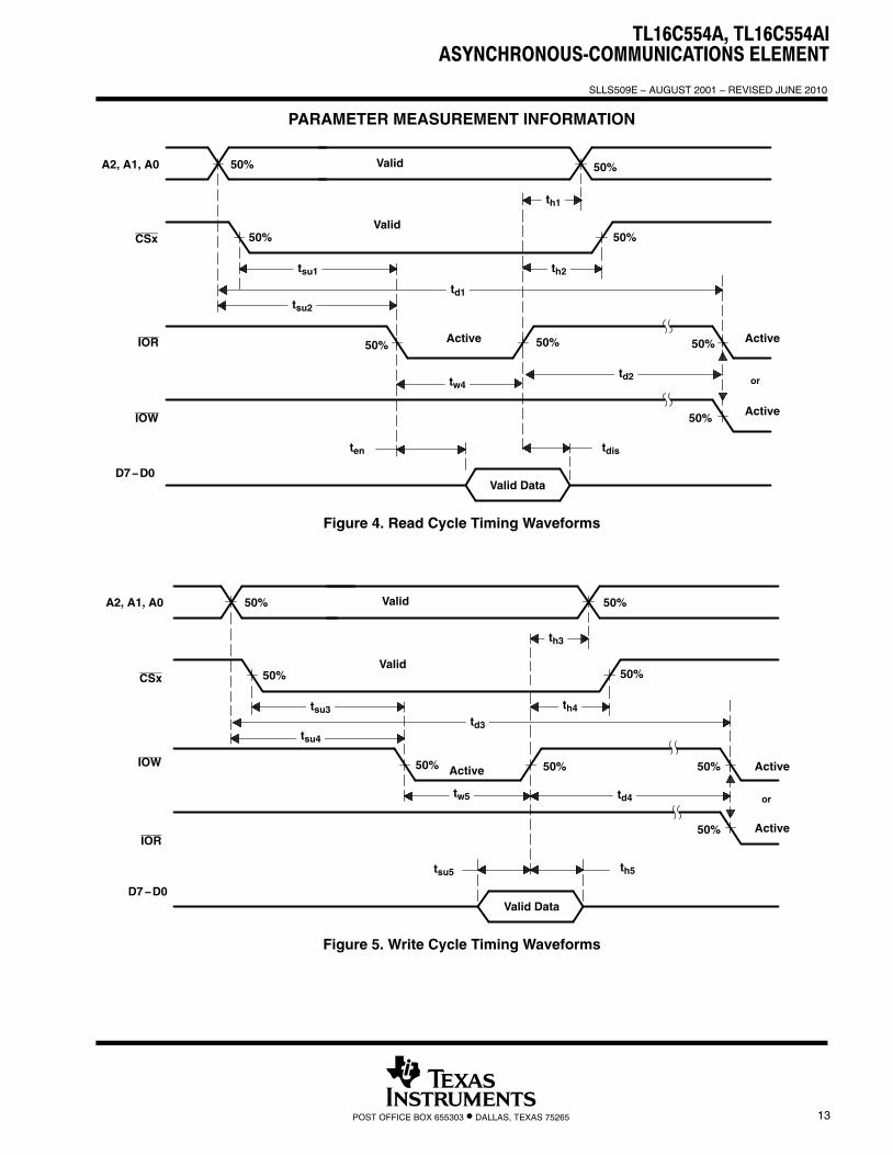
read cycle timing requirements over recommended ranges of operating free-air temperature andsupply voltage (see Figure 4)
MIN MAX UNIT
tw4 Pulse duration, IOR low 75 ns
tsu1 Setup time, CSx valid before IOR low (see Note 2) 10 ns
tsu2 Setup time, A2−A0 valid before IOR low (see Note 2) 15 ns
th1 Hold time, A2−A0 valid after IOR high (see Note 2) 0 ns
th2 Hold time, CSx valid after IOR high (see Note 2) 0 ns
td1 Delay time, tsu2 + tw4 + td2 (see Note 3) 140 ns
td2 Delay time, IOR high to IOR or IOW low 50 ns
NOTES: 2. The internal address strobe is always active.3. In the FIFO mode, td1 = 425 ns (min) between reads of the receiver FIFO and the status registers (interrupt-identification register
and line-status register).
write cycle timing requirements over recommended ranges of operating free-air temperature andsupply voltage (see Figure 5)
MIN MAX UNIT
tw5 Pulse duration, IOW↓ 50 ns
tsu3 Setup time, CSx valid before IOW↓ (see Note 2) 10 ns
tsu4 Setup time, A2−A0 valid before IOW↓ (see Note 2) 15 ns
tsu5 Setup time, D7−D0 valid before IOW↑ 10 ns
th3 Hold time, A2−A0 valid after IOW↑ (see Note 2) 5 ns
th4 Hold time, CSx valid after IOW↑ (see Note 2) 5 ns
th5 Hold time, D7−D0 valid after IOW↑ 25 ns
td3 Delay time, tsu4 + tw5 + td4 120 ns
td4 Delay time, IOW↑ to IOW or IOR↓ 55 ns
NOTE 2: The internal address strobe is always active.
read cycle switching characteristics over recommended ranges of operating free-air temperatureand supply voltage, CL = 100 pF (see Note 4 and Figure 4)
PARAMETER MIN MAX UNIT
ten Enable time, IOR↓ to D7−D0 valid 30 ns
tdis Disable time, IOR↑ to D7−D0 released 0 20 ns
NOTE 4: VOL and VOH (and the external loading) determine the charge and discharge time.
TL16C554A, TL16C554AIASYNCHRONOUS-COMMUNICATIONS ELEMENT
�
�
SLLS509E − AUGUST 2001 − REVISED JUNE 2010
11POST OFFICE BOX 655303 • DALLAS, TEXAS 75265
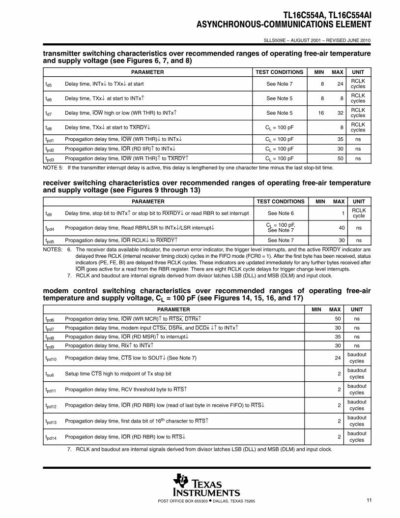
transmitter switching characteristics over recommended ranges of operating free-air temperatureand supply voltage (see Figures 6, 7, and 8)
PARAMETER TEST CONDITIONS MIN MAX UNIT
td5 Delay time, INTx↓ to TXx↓ at start See Note 7 8 24 RCLKcycles
td6 Delay time, TXx↓ at start to INTx↑ See Note 5 8 8 RCLKcycles
td7 Delay time, IOW high or low (WR THR) to INTx↑ See Note 5 16 32 RCLKcycles
td8 Delay time, TXx↓ at start to TXRDY↓ CL = 100 pF 8 RCLKcycles
tpd1 Propagation delay time, IOW (WR THR)↓ to INTx↓ CL = 100 pF 35 ns
tpd2 Propagation delay time, IOR (RD IIR)↑ to INTx↓ CL = 100 pF 30 ns
tpd3 Propagation delay time, IOW (WR THR)↑ to TXRDY↑ CL = 100 pF 50 ns
NOTE 5: If the transmitter interrupt delay is active, this delay is lengthened by one character time minus the last stop-bit time.
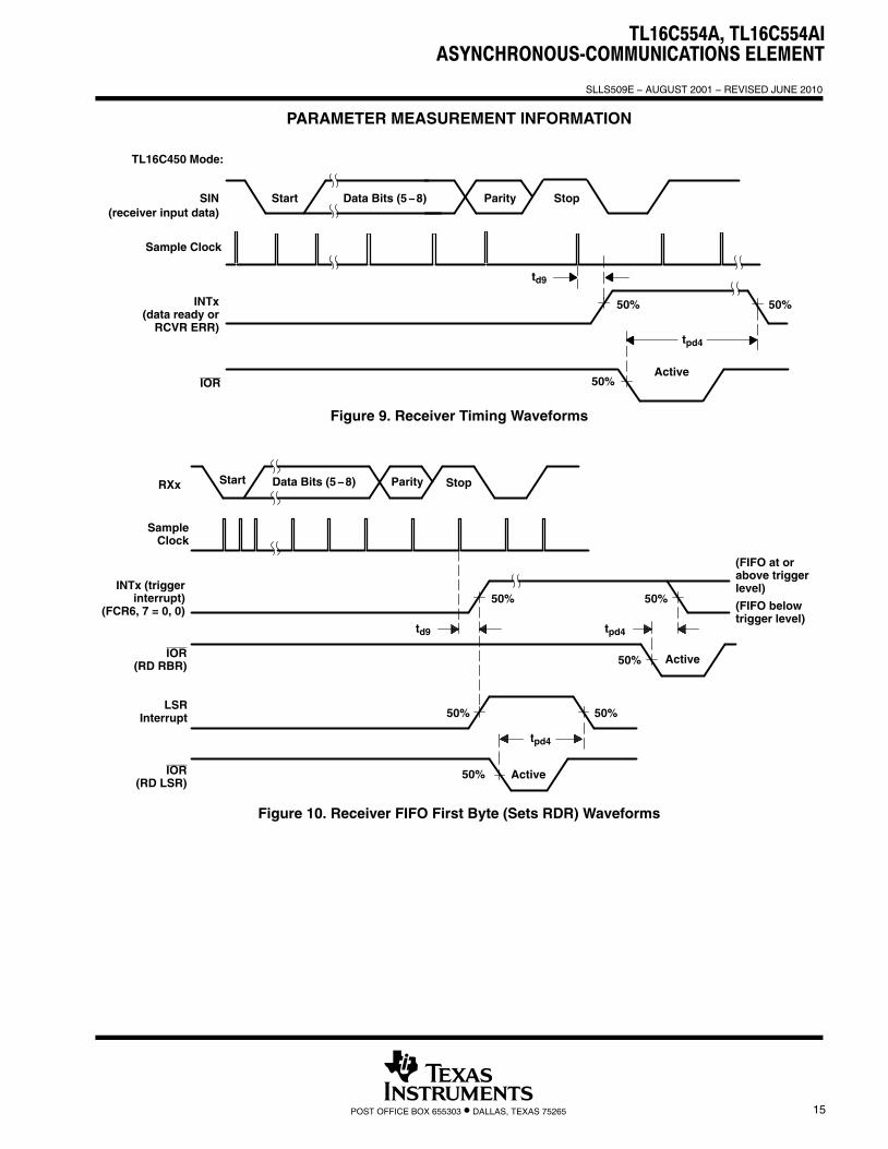
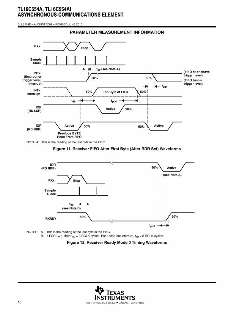
receiver switching characteristics over recommended ranges of operating free-air temperatureand supply voltage (see Figures 9 through 13)
PARAMETER TEST CONDITIONS MIN MAX UNIT
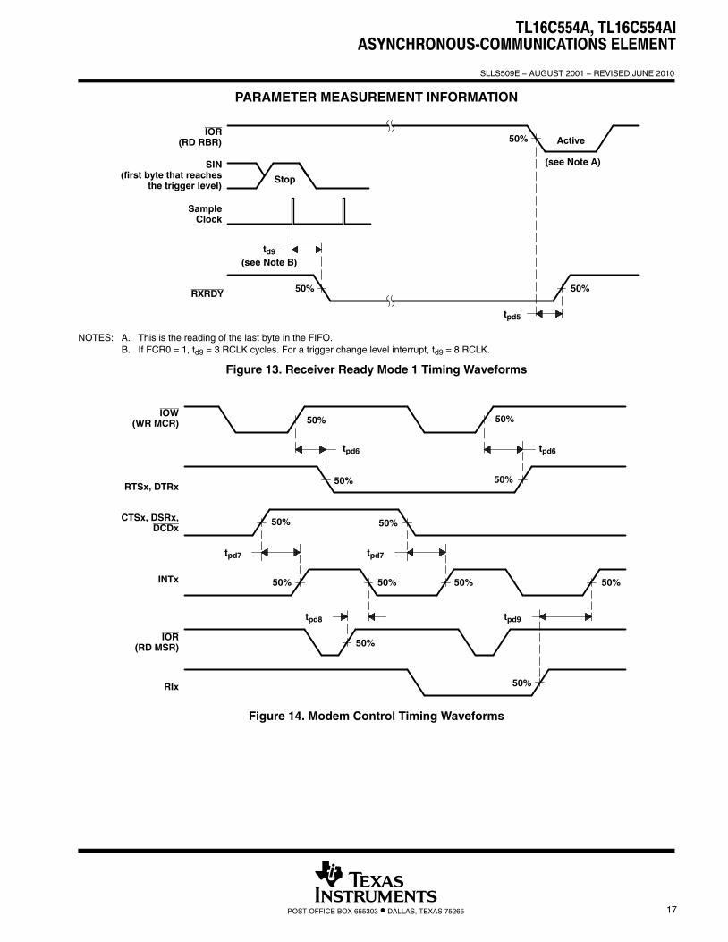
td9 Delay time, stop bit to INTx↑ or stop bit to RXRDY↓ or read RBR to set interrupt See Note 6 1 RCLKcycle
tpd4 Propagation delay time, Read RBR/LSR to INTx↓/LSR interrupt↓ CL = 100 pF,See Note 7 40 ns
tpd5 Propagation delay time, IOR RCLK↓ to RXRDY↑ See Note 7 30 ns
NOTES: 6. The receiver data available indicator, the overrun error indicator, the trigger level interrupts, and the active RXRDY indicator aredelayed three RCLK (internal receiver timing clock) cycles in the FIFO mode (FCR0 = 1). After the first byte has been received, statusindicators (PE, FE, BI) are delayed three RCLK cycles. These indicators are updated immediately for any further bytes received afterIOR goes active for a read from the RBR register. There are eight RCLK cycle delays for trigger change level interrupts.
7. RCLK and baudout are internal signals derived from divisor latches LSB (DLL) and MSB (DLM) and input clock.
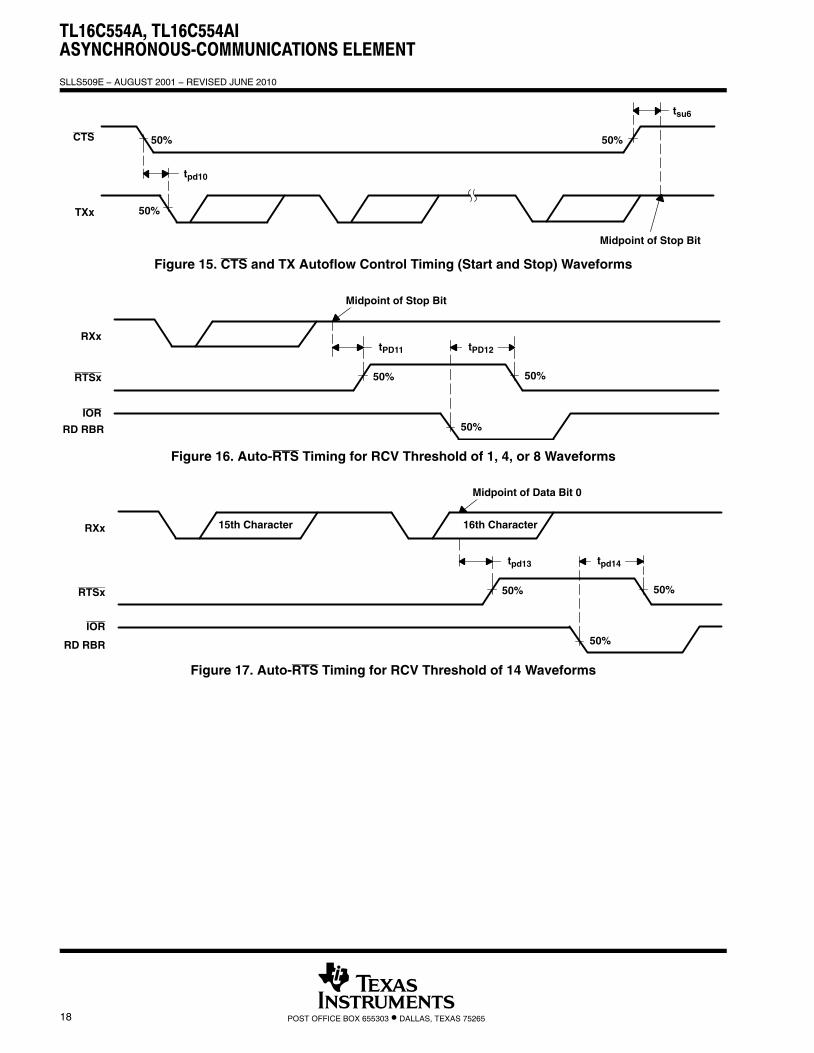
modem control switching characteristics over recommended ranges of operating free-airtemperature and supply voltage, CL = 100 pF (see Figures 14, 15, 16, and 17)
PARAMETER MIN MAX UNIT
tpd6 Propagation delay time, IOW (WR MCR)↑ to RTSx, DTRx↑ 50 ns
tpd7 Propagation delay time, modem input CTSx, DSRx, and DCDx ↓↑ to INTx↑ 30 ns
tpd8 Propagation delay time, IOR (RD MSR)↑ to interrupt↓ 35 ns
tpd9 Propagation delay time, RIx↑ to INTx↑ 30 ns
tpd10 Propagation delay time, CTS low to SOUT↓ (See Note 7) 24baudoutcycles
tsu6 Setup time CTS high to midpoint of Tx stop bit 2baudoutcycles
tpd11 Propagation delay time, RCV threshold byte to RTS↑ 2baudoutcycles
tpd12 Propagation delay time, IOR (RD RBR) low (read of last byte in receive FIFO) to RTS↓ 2baudoutcycles
tpd13 Propagation delay time, first data bit of 16th character to RTS↑ 2baudoutcycles
tpd14 Propagation delay time, IOR (RD RBR) low to RTS↓ 2baudoutcycles
7. RCLK and baudout are internal signals derived from divisor latches LSB (DLL) and MSB (DLM) and input clock.
TL16C554A, TL16C554AIASYNCHRONOUS-COMMUNICATIONS ELEMENT�
�
SLLS509E − AUGUST 2001 − REVISED JUNE 2010
12 POST OFFICE BOX 655303 • DALLAS, TEXAS 75265
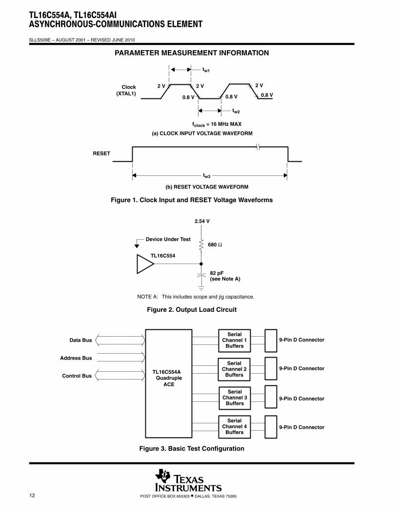
PARAMETER MEASUREMENT INFORMATION
Clock(XTAL1)
fclock = 16 MHz MAX
tw2
tw1
0.8 V
2 V
tw3
RESET
2 V2 V
0.8 V 0.8 V
(a) CLOCK INPUT VOLTAGE WAVEFORM
(b) RESET VOLTAGE WAVEFORM
Figure 1. Clock Input and RESET Voltage Waveforms
82 pF(see Note A)
680 Ω
2.54 V
Device Under Test
TL16C554
NOTE A: This includes scope and jig capacitance.
Figure 2. Output Load Circuit
9-Pin D ConnectorSerial
Channel 1Buffers
SerialChannel 2
Buffers
SerialChannel 3
Buffers
SerialChannel 4
Buffers
9-Pin D Connector
9-Pin D Connector
9-Pin D Connector
Data Bus
Address Bus
Control Bus QuadrupleACE
TL16C554A
Figure 3. Basic Test Configuration
TL16C554A, TL16C554AIASYNCHRONOUS-COMMUNICATIONS ELEMENT
�
�
SLLS509E − AUGUST 2001 − REVISED JUNE 2010
13POST OFFICE BOX 655303 • DALLAS, TEXAS 75265
PARAMETER MEASUREMENT INFORMATION
tw4td2
Active
ValidA2, A1, A0
Valid
Valid Data
IOR
IOW
D7−D0
th1
th2tsu1
tsu2
Active
td1
ten tdis
or
Active
CSx
50%
50%
50%
50% 50%
50%
50%
50%
Figure 4. Read Cycle Timing Waveforms
ValidA2, A1, A0
Valid
Valid Data
IOR
IOW
D7−D0
tsu3
tsu4
tw5
td3
th4
td4
tsu5 th5
Active
or
Active
th3
Active
CSx
50%
50%
50%
50% 50%
50%50%
50%
Figure 5. Write Cycle Timing Waveforms
TL16C554A, TL16C554AIASYNCHRONOUS-COMMUNICATIONS ELEMENT�
�
SLLS509E − AUGUST 2001 − REVISED JUNE 2010
14 POST OFFICE BOX 655303 • DALLAS, TEXAS 75265
PARAMETER MEASUREMENT INFORMATION
Start
IOR(RD IIR)
IOW(WR THR)
tpd1
td7
td5 td6
tpd2
StartData (5−8)
ParityStop (1−2)
tpd1
TXx
INTx
50%
50%50% 50%50% 50%
50%
50%50%50%
50%
Figure 6. Transmitter Timing Waveforms
Byte #1IOW(WR THR)
Data
td8
StartParity Stop
tpd3
TXRDY
TXx
FIFO Empty
50%
50%
50%50%
Figure 7. Transmitter Ready Mode 0 Timing Waveforms
IOW(WR THR)
TXRDY
Byte #16
Data
td8
StartParity Stop
tpd3
Start
FIFO Full
TXx
50%
50%
50%
50%
Figure 8. Transmitter Ready Mode 1 Timing Waveforms
TL16C554A, TL16C554AIASYNCHRONOUS-COMMUNICATIONS ELEMENT
�
�
SLLS509E − AUGUST 2001 − REVISED JUNE 2010
15POST OFFICE BOX 655303 • DALLAS, TEXAS 75265
PARAMETER MEASUREMENT INFORMATION
tpd4
Parity StopStart Data Bits (5−8)
TL16C450 Mode:
Sample Clock
SIN(receiver input data)
INTx(data ready or
RCVR ERR)
IOR
td9
Active
50% 50%
50%
Figure 9. Receiver Timing Waveforms
Start Data Bits (5−8) Parity Stop
SampleClock
td9 tpd4
INTx (triggerinterrupt)
(FCR6, 7 = 0, 0)
(FIFO at orabove triggerlevel)
(FIFO belowtrigger level)
ActiveIOR(RD RBR)
IOR(RD LSR)
tpd4
Active
RXx
LSRInterrupt
50%50%
50%
50%50%
50%
Figure 10. Receiver FIFO First Byte (Sets RDR) Waveforms
TL16C554A, TL16C554AIASYNCHRONOUS-COMMUNICATIONS ELEMENT�
�
SLLS509E − AUGUST 2001 − REVISED JUNE 2010
16 POST OFFICE BOX 655303 • DALLAS, TEXAS 75265
PARAMETER MEASUREMENT INFORMATION
Stop
td9 (see Note A)
tpd4
Top Byte of FIFO
tpd4td9
Active Active
SampleClock
INTx (time-out or
trigger level)Interrupt
IOR(RD RBR)
IOR(RD LSR)
Previous BYTERead From FIFO
Active
(FIFO at or abovetrigger level)
(FIFO belowtrigger level)
RXx
INTxInterrupt
50%50%
50%
50% 50%
50%50%
NOTE A: This is the reading of the last byte in the FIFO.
Figure 11. Receiver FIFO After First Byte (After RDR Set) Waveforms
Active
(see Note A)
Stop
td9
(see Note B)
tpd5
IOR(RD RBR)
SampleClock
RXRDY
RXx
50%50%
50%
NOTES: A. This is the reading of the last byte in the FIFO.B. If FCR0 = 1, then td9 = 3 RCLK cycles. For a time-out interrupt, td9 = 8 RCLK cycles.
Figure 12. Receiver Ready Mode 0 Timing Waveforms
TL16C554A, TL16C554AIASYNCHRONOUS-COMMUNICATIONS ELEMENT
�
�
SLLS509E − AUGUST 2001 − REVISED JUNE 2010
17POST OFFICE BOX 655303 • DALLAS, TEXAS 75265
PARAMETER MEASUREMENT INFORMATION
Active
(see Note A)
Stop
td9
(see Note B)
tpd5
IOR(RD RBR)
SIN(first byte that reaches
the trigger level)
SampleClock
RXRDY50%
50%
50%
NOTES: A. This is the reading of the last byte in the FIFO.B. If FCR0 = 1, td9 = 3 RCLK cycles. For a trigger change level interrupt, td9 = 8 RCLK.
Figure 13. Receiver Ready Mode 1 Timing Waveforms
tpd6 tpd6
tpd7 tpd7
tpd8 tpd9
IOW(WR MCR)
IOR(RD MSR)
RTSx, DTRx
CTSx, DSRx,DCDx
RIx
INTx
50%50%
50%50%
50%50%
50%50% 50%
50%
50%
50%
Figure 14. Modem Control Timing Waveforms
TL16C554A, TL16C554AIASYNCHRONOUS-COMMUNICATIONS ELEMENT�
�
SLLS509E − AUGUST 2001 − REVISED JUNE 2010
18 POST OFFICE BOX 655303 • DALLAS, TEXAS 75265
Midpoint of Stop Bit
tpd10
tsu6
CTS
TXx
50% 50%
50%
Figure 15. CTS and TX Autoflow Control Timing (Start and Stop) Waveforms
tPD12
RXx
50%
tPD11
50%
50%
Midpoint of Stop Bit
RTSx
RD RBR
IOR
Figure 16. Auto-RTS Timing for RCV Threshold of 1, 4, or 8 Waveforms
tpd14
RXx
50%
tpd13
50%
50%
Midpoint of Data Bit 0
RTSx
RD RBR
15th Character 16th Character
IOR
Figure 17. Auto-RTS Timing for RCV Threshold of 14 Waveforms
TL16C554A, TL16C554AIASYNCHRONOUS-COMMUNICATIONS ELEMENT
�
�
SLLS509E − AUGUST 2001 − REVISED JUNE 2010
19POST OFFICE BOX 655303 • DALLAS, TEXAS 75265
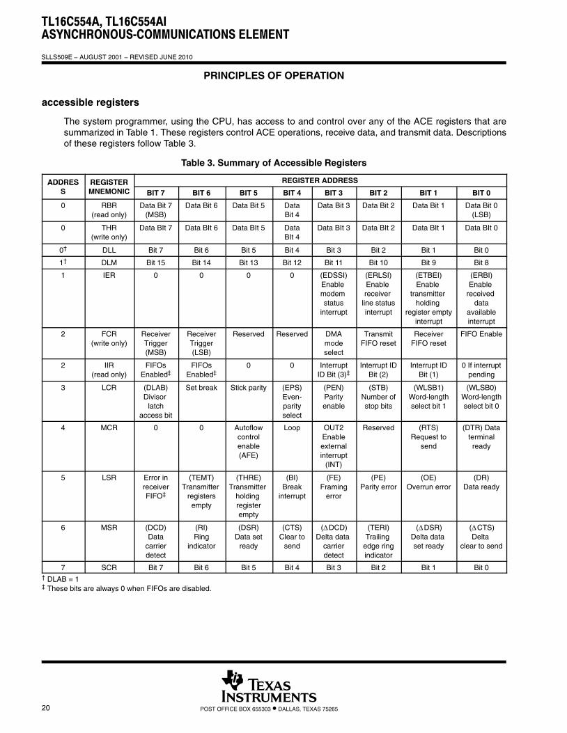
PRINCIPLES OF OPERATION
Three types of information are stored in the internal registers used in the ACE: control, status, and data. Mnemonicabbreviations for the registers are shown in Table 1. Table 2 defines the address location of each register and whetherit is read only, write only, or read writable.
Table 1. Internal Register Mnemonic Abbreviations
CONTROL MNEMONIC STATUS MNEMONIC DATA MNEMONIC
Line-control register LCR Line-status register LSR Receiver-buffer register RBR
FIFO-control register FCR Modem-status register MSR Transmitter-holding register THR
Modem-control register MCR
Divisor-latch LSB DLL
Divisor-latch MSB DLM
Interrupt enable register IER
Table 2. Register Selection†
DLAB‡ A2§ A1§ A0§ READ MODE WRITE MODE
0 0 0 0 Receiver-buffer register Transmitter-holding register
0 0 0 1 Interrupt-enable register
X 0 1 0 Interrupt-identification register FIFO-control register
X 0 1 1 Line-control register
X 1 0 0 Modem-control register
X 1 0 1 Line-status register
X 1 1 0 Modem-status register
X 1 1 1 Scratchpad register Scratchpad register
1 0 0 0 LSB divisor-latch
1 0 0 1 MSB divisor-latch
X = irrelevant, 0 = low level, 1 = high level† The serial channel is accessed when either CSA or CSD is low.‡ DLAB is the divisor-latch access bit, located in bit 7 of the LCR.§ A2−A0 are device terminals.
Individual bits within the registers with the bit number in parenthesis are referred to by the register mnemonic. Forexample, LCR7 refers to line-control register bit 7. The transmitter-buffer register and the receiver-buffer register aredata registers that hold from five to eight bits of data. If less than eight data bits are transmitted, data is right-justifiedto the LSB. Bit 0 of a data word is always the first serial-data bit received and transmitted. The ACE data registersare double buffered (TL16450 mode) or FIFO buffered (FIFO mode) so that read and write operations can beperformed when the ACE is performing the parallel-to-serial or serial-to-parallel conversion.
TL16C554A, TL16C554AIASYNCHRONOUS-COMMUNICATIONS ELEMENT�
�
SLLS509E − AUGUST 2001 − REVISED JUNE 2010
20 POST OFFICE BOX 655303 • DALLAS, TEXAS 75265
PRINCIPLES OF OPERATION
accessible registers
The system programmer, using the CPU, has access to and control over any of the ACE registers that aresummarized in Table 1. These registers control ACE operations, receive data, and transmit data. Descriptionsof these registers follow Table 3.
Table 3. Summary of Accessible Registers
ADDRES REGISTER REGISTER ADDRESSADDRESS
REGISTERMNEMONIC BIT 7 BIT 6 BIT 5 BIT 4 BIT 3 BIT 2 BIT 1 BIT 0
0 RBR(read only)
Data Bit 7(MSB)
Data Bit 6 Data Bit 5 DataBit 4
Data Bit 3 Data Bit 2 Data Bit 1 Data Bit 0(LSB)
0 THR(write only)
Data BIt 7 Data BIt 6 Data BIt 5 DataBIt 4
Data BIt 3 Data BIt 2 Data BIt 1 Data BIt 0
0† DLL Bit 7 Bit 6 Bit 5 Bit 4 Bit 3 Bit 2 Bit 1 Bit 0
1† DLM Bit 15 Bit 14 Bit 13 Bit 12 Bit 11 Bit 10 Bit 9 Bit 8
1 IER 0 0 0 0 (EDSSI)Enable modem status
interrupt
(ERLSI)Enable receiver
line statusinterrupt
(ETBEI)Enable
transmitter holding
register emptyinterrupt
(ERBI)Enable
received data
availableinterrupt
2 FCR(write only)
ReceiverTrigger(MSB)
ReceiverTrigger(LSB)
Reserved Reserved DMAmodeselect
TransmitFIFO reset
ReceiverFIFO reset
FIFO Enable
2 IIR(read only)
FIFOsEnabled‡
FIFOsEnabled‡
0 0 InterruptID Bit (3)‡
Interrupt IDBit (2)
Interrupt IDBit (1)
0 If interruptpending
3 LCR (DLAB)Divisor
latchaccess bit
Set break Stick parity (EPS)Even-parityselect
(PEN)Parityenable
(STB)Number ofstop bits
(WLSB1)Word-lengthselect bit 1
(WLSB0)Word-lengthselect bit 0
4 MCR 0 0 Autoflowcontrolenable(AFE)
Loop OUT2Enableexternalinterrupt
(INT)
Reserved (RTS)Request to
send
(DTR) Dataterminalready
5 LSR Error inreceiverFIFO‡
(TEMT)Transmitter
registersempty
(THRE)Transmitter
holding registerempty
(BI)Break
interrupt
(FE)Framing
error
(PE)Parity error
(OE)Overrun error
(DR)Data ready
6 MSR (DCD)Data
carrierdetect
(RI)Ring
indicator
(DSR)Data set
ready
(CTS)Clear to
send
(ΔDCD)Delta data
carrierdetect
(TERI)Trailing
edge ringindicator
(ΔDSR)Delta data set ready
(ΔCTS)Delta
clear to send
7 SCR Bit 7 Bit 6 Bit 5 Bit 4 Bit 3 Bit 2 Bit 1 Bit 0† DLAB = 1‡ These bits are always 0 when FIFOs are disabled.
TL16C554A, TL16C554AIASYNCHRONOUS-COMMUNICATIONS ELEMENT
�
�
SLLS509E − AUGUST 2001 − REVISED JUNE 2010
21POST OFFICE BOX 655303 • DALLAS, TEXAS 75265
PRINCIPLES OF OPERATION
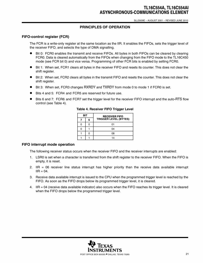
FIFO-control register (FCR)
The FCR is a write-only register at the same location as the IIR. It enables the FIFOs, sets the trigger level ofthe receiver FIFO, and selects the type of DMA signalling.
� Bit 0: FCR0 enables the transmit and receive FIFOs. All bytes in both FIFOs can be cleared by clearingFCR0. Data is cleared automatically from the FIFOs when changing from the FIFO mode to the TL16C450mode (see FCR bit 0) and vice versa. Programming of other FCR bits is enabled by setting FCR0.
� Bit 1: When set, FCR1 clears all bytes in the receiver FIFO and resets its counter. This does not clear theshift register.
� Bit 2: When set, FCR2 clears all bytes in the transmit FIFO and resets the counter. This does not clear theshift register.
� Bit 3: When set, FCR3 changes RXRDY and TXRDY from mode 0 to mode 1 if FCR0 is set.
� Bits 4 and 5: FCR4 and FCR5 are reserved for future use.
� Bits 6 and 7: FCR6 and FCR7 set the trigger level for the receiver FIFO interrupt and the auto-RTS flowcontrol (see Table 4).
Table 4. Receiver FIFO Trigger Level
BIT RECEIVER FIFO7 6
RECEIVER FIFOTRIGGER LEVEL (BYTES)
0 0 01
0 1 04
1 0 08
1 1 14
FIFO interrupt mode operation
The following receiver status occurs when the receiver FIFO and the receiver interrupts are enabled:
1. LSR0 is set when a character is transferred from the shift register to the receiver FIFO. When the FIFO isempty, it is reset.
2. IIR = 06 receiver line status interrupt has higher priority than the receive data available interruptIIR = 04.
3. Receive data available interrupt is issued to the CPU when the programmed trigger level is reached by theFIFO. As soon as the FIFO drops below its programmed trigger level, it is cleared.
4. IIR = 04 (receive data available indicator) also occurs when the FIFO reaches its trigger level. It is clearedwhen the FIFO drops below the programmed trigger level.
TL16C554A, TL16C554AIASYNCHRONOUS-COMMUNICATIONS ELEMENT�
�
SLLS509E − AUGUST 2001 − REVISED JUNE 2010
22 POST OFFICE BOX 655303 • DALLAS, TEXAS 75265
PRINCIPLES OF OPERATION
FIFO interrupt mode operation (continued)
The following receiver FIFO character time-out status occurs when receiver FIFO and the receiver interruptsare enabled.
1. When the following conditions exist, a FIFO character time-out interrupt occurs:
a. Minimum of one character in FIFO
b. No new serial characters have been received for at least four character times. At 300 baud and 12-bitcharacters, the FIFO time-out interrupt causes a latency of 160 ms maximum from received characterto interrupt generation.
c. The receive FIFO has not been read for at least four character times.
2. By using the XTAL1 input for a clock signal, the character times can be calculated. The delay is proportionalto the baud rate.
3. The time-out timer is reset after the CPU reads the receiver FIFO or after a new character is received. Thisoccurs when there has been no time-out interrupt.
4. A time-out interrupt is cleared and the timer is reset when the CPU reads a character from the receiver FIFO.
Transmit interrupts occurs as follows when the transmitter and transmit FIFO interrupts are enabled(FCR0 =1, IER1 = 1).
1. When the transmitter FIFO is empty, the transmitter holding register interrupt (IIR = 02) occurs. The interruptis cleared when the transmitter holding register is written to or the IIR is read. One to sixteen characters canbe written to the transmit FIFO when servicing this interrupt.
2. The transmitter FIFO empty indicators are delayed one character time minus the last stop-bit time wheneverthe following occurs:
THRE = 1, and there have not been at least two bytes in transmit FIFO since the last THRE = 1. The firsttransmitter interrupt comes immediately after changing FCR0, assuming the interrupt is enabled.
Receiver FIFO trigger level and character time-out interrupts have the same priority as the receive dataavailable interrupt. The transmitter holding register empty interrupt has the same priority as the transmitter FIFOempty interrupt.
FIFO polled mode operation
When the FIFOs are enabled and all interrupts are disabled, the device is in the FIFO polled mode.
In the FIFO polled mode, there is no time-out condition indicated or trigger level reached. However, the receiveand transmit FIFOs still have the capability of holding characters. The LSR must be read to determine the ACEstatus.
TL16C554A, TL16C554AIASYNCHRONOUS-COMMUNICATIONS ELEMENT
�
�
SLLS509E − AUGUST 2001 − REVISED JUNE 2010
23POST OFFICE BOX 655303 • DALLAS, TEXAS 75265
PRINCIPLES OF OPERATION
interrupt-enable register (IER)
The IER independently enables the four serial channel interrupt sources that activate the interrupt (INTA, B, C,D) output. All interrupts are disabled by clearing IER0 − IER3 of the IER. Interrupts are enabled by setting theappropriate bits of the IER. Disabling the interrupt system inhibits the IIR and the active (high) interrupt output.All other system functions operate in their normal manner, including the setting of the LSR and MSR. Thecontents of the IER are shown in Table 3 and described in the following bulleted list:
� Bit 0: When IER0 is set, IER0 enables the received data available interrupt and the timeout interrupts inthe FIFO mode.
� Bit 1: When IER1 is set, the transmitter holding register empty interrupt is enabled.
� Bit 2: When IER2 is set, the receiver line status interrupt is enabled.
� Bit 3: When IER3 is set, the modem-status interrupt is enabled.
� Bits 4 − 7: IER4 − IER7. These four bits of the IER are cleared.
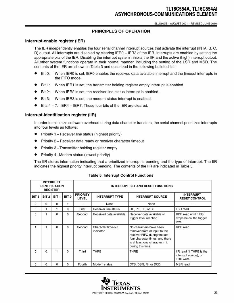
interrupt-identification register (IIR)
In order to minimize software overhead during data character transfers, the serial channel prioritizes interruptsinto four levels as follows:
� Priority 1 − Receiver line status (highest priority)
� Priority 2 − Receiver data ready or receiver character timeout
� Priority 3 −Transmitter holding register empty
� Priority 4−Modem status (lowest priority)
The IIR stores information indicating that a prioritized interrupt is pending and the type of interrupt. The IIRindicates the highest priority interrupt pending. The contents of the IIR are indicated in Table 5.
Table 5. Interrupt Control Functions
INTERRUPTIDENTIFICATION
REGISTERINTERRUPT SET AND RESET FUNCTIONS
BIT 3 BIT 2 BIT 1 BIT 0PRIORITY
LEVEL INTERRUPT TYPE INTERRUPT SOURCEINTERRUPT
RESET CONTROL
0 0 0 1 — None None —
0 1 1 0 First Receiver line status OE, PE, FE, or BI LSR read
0 1 0 0 Second Received data available Receiver data available ortrigger level reached
RBR read until FIFOdrops below the triggerlevel
1 1 0 0 Second Character time-outindicator
No characters have beenremoved from or input to thereceiver FIFO during the lastfour character times, and thereis at least one character in itduring this time.
RBR read
0 0 1 0 Third THRE THRE IIR read (if THRE is theinterrupt source), orTHR write
0 0 0 0 Fourth Modem status CTS, DSR, RI, or DCD MSR read
TL16C554A, TL16C554AIASYNCHRONOUS-COMMUNICATIONS ELEMENT�
�
SLLS509E − AUGUST 2001 − REVISED JUNE 2010
24 POST OFFICE BOX 655303 • DALLAS, TEXAS 75265
PRINCIPLES OF OPERATION
interrupt-identification register (IIR) (continued)
� Bit 0: IIR0 indicates whether an interrupt is pending. When IIR0 is cleared, an interrupt is pending.
� Bits 1 and 2: IIR1 and IIR2 identify the highest priority interrupt pending as indicated in Table 5.
� Bit 3: IIR3 is always cleared in the TL16C450 mode. This bit, along with bit 2, is set when in the FIFO modeand a character time-out interrupt is pending.
� Bits 4 and 5: IIR4 and IIR5 are always cleared.
� Bits 6 and 7: IIR6 and IIR7 are set when FCR0 = 1.
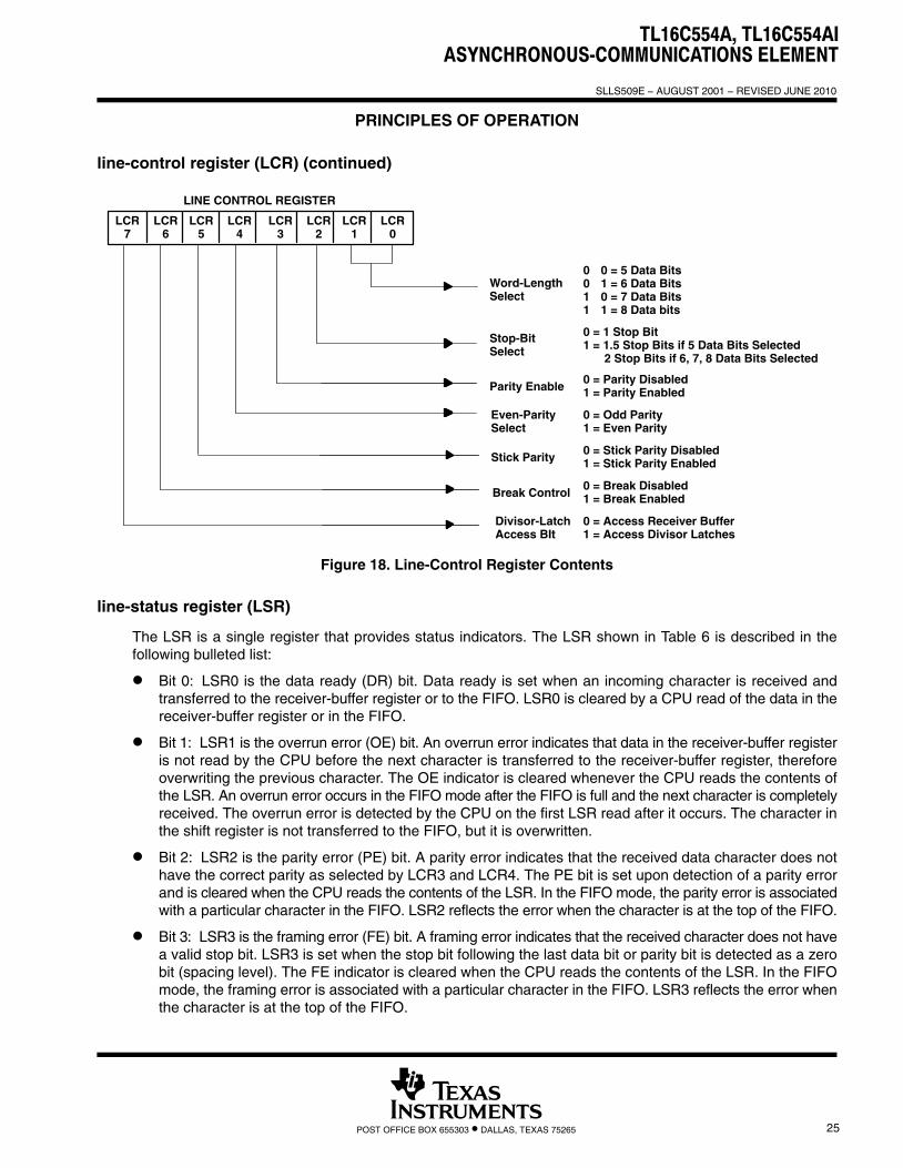
line-control register (LCR)
The format of the data character is controlled by LCR. LCR may be read. Its contents are described in thefollowing bulleted list and shown in Figure 18.
� Bits 0 and 1: LCR0 and LCR1 are word-length select bits. These bits program the number of bits in eachserial character and are shown in Figure 18.
� Bit 2: LCR2 is the stop-bit select bit. This bit specifies the number of stop bits in each transmitted character.The receiver always checks for one stop bit.
� Bit 3: LCR3 is the parity-enable bit. When LCR3 is set, a parity bit between the last data word bit and thestop bit is generated and checked.
� Bit 4: LCR4 is the even-parity select bit. When this bit is set and parity is enabled (LCR3 is set), even parityis selected. When this bit is cleared and parity is enabled, odd parity is selected.
� Bit 5: LCR5 is the stick-parity bit. When parity is enabled (LCR3 is set) and this bit is set, the transmissionand reception of a parity bit is placed in the opposite state from the value of LCR4. This forces parity to aknown state and allows the receiver to check the parity bit in a known state.
� Bit 6: LCR6 is a break-control bit. When this bit is set, the serial outputs TXx are forced to the spacing state(low). The break-control bit acts only on the serial output and does not affect the transmitter logic. If thefollowing sequence is used, no invalid characters are transmitted because of the break.
Step 1. Load a zero byte in response to the transmitter holding register empty (THRE) status indicator.
Step 2. Set the break in response to the next THRE status indicator.
Step 3. Wait for the transmitter to be idle when transmitter empty status signal is set (TEMT = 1); thenclear the break when the normal transmission has to be restored.
� Bit 7: LCR7 is the divisor-latch access bit (DLAB) bit. This bit must be set to access the divisor latches DLLand DLM of the baud-rate generator during a read or write operation. LCR7 must be cleared to access thereceiver-buffer register, the transmitter-holding register, or the interrupt-enable register.
TL16C554A, TL16C554AIASYNCHRONOUS-COMMUNICATIONS ELEMENT
�
�
SLLS509E − AUGUST 2001 − REVISED JUNE 2010
25POST OFFICE BOX 655303 • DALLAS, TEXAS 75265
PRINCIPLES OF OPERATION
line-control register (LCR) (continued)
Word-LengthSelect
0 0 = 5 Data Bits0 1 = 6 Data Bits1 0 = 7 Data Bits1 1 = 8 Data bits
LINE CONTROL REGISTER
LCR7
LCR6
LCR5
LCR4
LCR3
LCR2
LCR1
LCR0
Stop-BitSelect
0 = 1 Stop Bit1 = 1.5 Stop Bits if 5 Data Bits Selected
2 Stop Bits if 6, 7, 8 Data Bits Selected
Parity Enable0 = Parity Disabled1 = Parity Enabled
Even-Parity Select
0 = Odd Parity1 = Even Parity
Stick Parity0 = Stick Parity Disabled1 = Stick Parity Enabled
Break Control0 = Break Disabled1 = Break Enabled
Divisor-LatchAccess BIt
0 = Access Receiver Buffer1 = Access Divisor Latches
Figure 18. Line-Control Register Contents
line-status register (LSR)
The LSR is a single register that provides status indicators. The LSR shown in Table 6 is described in thefollowing bulleted list:
� Bit 0: LSR0 is the data ready (DR) bit. Data ready is set when an incoming character is received andtransferred to the receiver-buffer register or to the FIFO. LSR0 is cleared by a CPU read of the data in thereceiver-buffer register or in the FIFO.
� Bit 1: LSR1 is the overrun error (OE) bit. An overrun error indicates that data in the receiver-buffer registeris not read by the CPU before the next character is transferred to the receiver-buffer register, thereforeoverwriting the previous character. The OE indicator is cleared whenever the CPU reads the contents ofthe LSR. An overrun error occurs in the FIFO mode after the FIFO is full and the next character is completelyreceived. The overrun error is detected by the CPU on the first LSR read after it occurs. The character inthe shift register is not transferred to the FIFO, but it is overwritten.
� Bit 2: LSR2 is the parity error (PE) bit. A parity error indicates that the received data character does nothave the correct parity as selected by LCR3 and LCR4. The PE bit is set upon detection of a parity errorand is cleared when the CPU reads the contents of the LSR. In the FIFO mode, the parity error is associatedwith a particular character in the FIFO. LSR2 reflects the error when the character is at the top of the FIFO.
� Bit 3: LSR3 is the framing error (FE) bit. A framing error indicates that the received character does not havea valid stop bit. LSR3 is set when the stop bit following the last data bit or parity bit is detected as a zerobit (spacing level). The FE indicator is cleared when the CPU reads the contents of the LSR. In the FIFOmode, the framing error is associated with a particular character in the FIFO. LSR3 reflects the error whenthe character is at the top of the FIFO.
TL16C554A, TL16C554AIASYNCHRONOUS-COMMUNICATIONS ELEMENT�
�
SLLS509E − AUGUST 2001 − REVISED JUNE 2010
26 POST OFFICE BOX 655303 • DALLAS, TEXAS 75265
PRINCIPLES OF OPERATION
line-status register (LSR) (continued)
� Bit 4: LSR4 is the break interrupt (BI) bit. Break interrupt is set when the received data input is held in thespacing (low) state for longer than a full word transmission time (start bit + data bits + parity + stop bits).The BI indicator is cleared when the CPU reads the contents of the LSR. In the FIFO mode, this is associatedwith a particular character in the FIFO. LSR2 reflects the BI when the break character is at the top of theFIFO. The error is detected by the CPU when its associated character is at the top of the FIFO during thefirst LSR read. Only one zero character is loaded into the FIFO when BI occurs.
LSR1 − LSR4 are the error conditions that produce a receiver line status interrupt (priority 1 interrupt in theinterrupt-identification register) when any of the conditions are detected. This interrupt is enabled by settingIER2 in the interrupt-enable register.
� Bit 5: LSR5 is the transmitter holding register empty (THRE) bit. THRE indicates that the ACE is ready toaccept a new character for transmission. The THRE bit is set when a character is transferred from thetransmitter holding register (THR) to the transmitter shift register (TSR). LSR5 is cleared when the CPUloads THR. LSR5 is not cleared by a CPU read of the LSR. In the FIFO mode, this bit is set when the transmitFIFO is empty, and it is cleared when one byte is written to the transmit FIFO. When the THRE interruptis enabled by IER1, THRE causes a priority 3 interrupt in the IIR. If THRE is the interrupt source indicatedby IIR, INTRPT is cleared by a read of the IIR.
� Bit 6: LSR6 is the transmitter register empty (TEMT) bit. TEMT is set when both THR and TSR are empty.LSR6 is cleared when a character is loaded into THR, and remains low until the character is transferred outof TXx. TEMT is not cleared by a CPU read of the LSR. In the FIFO mode, this bit is set when both thetransmitter FIFO and shift register are empty.
� Bit 7: LSR7 is the receiver FIFO error bit. The LSR7 bit is cleared in the TL16C450 mode (see FCR bit 0).In the FIFO mode, it is set when at least one of the following data errors is in the FIFO: parity error, framingerror, or break interrupt indicator. It is cleared when the CPU reads the LSR, unless there are subsequenterrors in the FIFO.
NOTEThe LSR may be written. However, this function is intended only for factory test. It should be considered as readonly by applications software.
Table 6. Line-Status Register BIts
LSR BITS 1 0
LSR0 data ready (DR) Ready Not ready
LSR1 overrun error (OE) Error No error
LSR2 parity error (PE) Error No error
LSR3 framing error (FE) Error No error
LSR4 break interrupt (BI) Break No break
LSR5 transmitter holding register empty (THRE) Empty Not empty
LSR6 transmitter register empty (TEMT) Empty Not empty
LSR7 receiver FIFO error Error in FIFO No error in FIFO
TL16C554A, TL16C554AIASYNCHRONOUS-COMMUNICATIONS ELEMENT
�
�
SLLS509E − AUGUST 2001 − REVISED JUNE 2010
27POST OFFICE BOX 655303 • DALLAS, TEXAS 75265
PRINCIPLES OF OPERATION
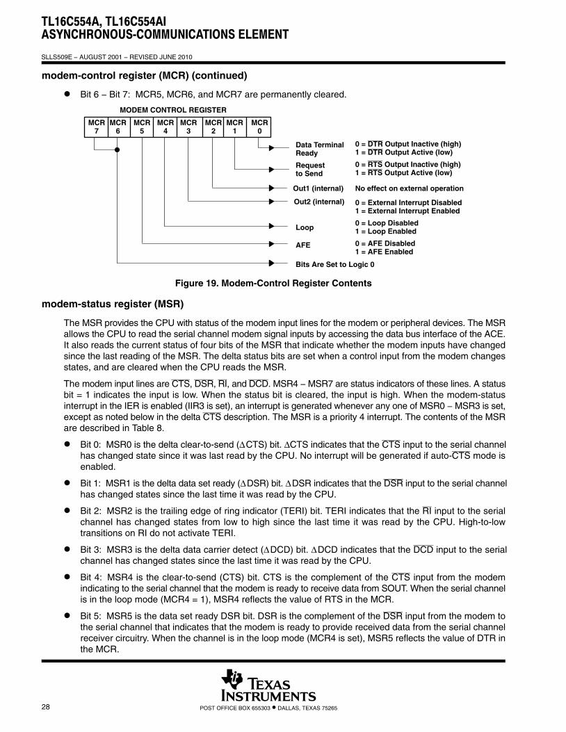
modem-control register (MCR)
The MCR controls the interface with the modem or data set as described in Figure 19. The MCR can be writtenand read. Outputs RTS and DTR are directly controlled by their control bits in this register. A high input assertsa low signal (active) at the output terminals. MCR bits 0, 1, 2, 3, and 4 are shown as follows:
� Bit 0: When MCR0 is set, the DTR output is forced low. When MCR0 is cleared, the DTR output is forcedhigh. The DTR output of the serial channel may be input into an inverting line driver in order to obtain theproper polarity input at the modem or data set.
� Bit1: When MCR1 is set, the RTS output is forced low. When MCR1 is cleared, the RTS output is forcedhigh. The RTS output of the serial channel may be input into an inverting line driver to obtain the properpolarity input at the modem or data set.
� Bit 2: MCR2 has no effect on operation.
� Bit 3: When MCR3 is set, the external serial channel interrupt is enabled.
� Bit 4: MCR4 provides a local loopback feature for diagnostic testing of the channel. When MCR4 is set,serial output TXx is set to the marking (high) state and SIN is disconnected. The output of the TSR is loopedback into the RSR input. The four modem control inputs (CTS, DSR, DCD, and RI) are disconnected. Thefour modem control output bits (DTR, RTS, OUT1, and OUT2) are internally connected to the four modemcontrol input bits (DSR, CTS, RI, and DCD), respectively. The modem control output terminals are forcedto their inactive (high) state. In the diagnostic mode, data transmitted is received by its own receiver. Thisallows the processor to verify the transmit and receive data paths of the selected serial channel. Interruptcontrol is fully operational; however, modem-status interrupts are generated by controlling the lower fourMCR bits internally. Interrupts are not generated by activity on the external terminals represented by thosefour bits.
� Bit 5: This bit is the autoflow control enable (AFE). When set, the autoflow control is enabled, as describedin the detailed description.
The ACE flow control can be configured by programming bits 1 and 5 of the MCR, as shown in Table 7.
Table 7. ACE Flow Configuration
MSR BIT 5(AFE)
MSR BIT 1(RTS)
ACE FLOW CONFIGURATION
1 1 Auto-RTS and auto-CTS enabled (autoflow control enabled)
1 0 Auto-CTS only enabled
0 X Auto-RTS and auto-CTS disabled
TL16C554A, TL16C554AIASYNCHRONOUS-COMMUNICATIONS ELEMENT�
�
SLLS509E − AUGUST 2001 − REVISED JUNE 2010
28 POST OFFICE BOX 655303 • DALLAS, TEXAS 75265
modem-control register (MCR) (continued)
� Bit 6 − Bit 7: MCR5, MCR6, and MCR7 are permanently cleared.
Data TerminalReady
0 = DTR Output Inactive (high)1 = DTR Output Active (low)
MODEM CONTROL REGISTER
MCR7
MCR6
MCR5
MCR4
MCR3
MCR2
Loop0 = Loop Disabled1 = Loop Enabled
Bits Are Set to Logic 0
Requestto Send
0 = RTS Output Inactive (high)1 = RTS Output Active (low)
MCR1
MCR0
Out1 (internal)
Out2 (internal)
No effect on external operation
0 = External Interrupt Disabled1 = External Interrupt Enabled
AFE 0 = AFE Disabled1 = AFE Enabled
Figure 19. Modem-Control Register Contents
modem-status register (MSR)
The MSR provides the CPU with status of the modem input lines for the modem or peripheral devices. The MSRallows the CPU to read the serial channel modem signal inputs by accessing the data bus interface of the ACE.It also reads the current status of four bits of the MSR that indicate whether the modem inputs have changedsince the last reading of the MSR. The delta status bits are set when a control input from the modem changesstates, and are cleared when the CPU reads the MSR.
The modem input lines are CTS, DSR, RI, and DCD. MSR4 − MSR7 are status indicators of these lines. A statusbit = 1 indicates the input is low. When the status bit is cleared, the input is high. When the modem-statusinterrupt in the IER is enabled (IIR3 is set), an interrupt is generated whenever any one of MSR0 − MSR3 is set,except as noted below in the delta CTS description. The MSR is a priority 4 interrupt. The contents of the MSRare described in Table 8.
� Bit 0: MSR0 is the delta clear-to-send (ΔCTS) bit. ΔCTS indicates that the CTS input to the serial channelhas changed state since it was last read by the CPU. No interrupt will be generated if auto-CTS mode isenabled.
� Bit 1: MSR1 is the delta data set ready (ΔDSR) bit. ΔDSR indicates that the DSR input to the serial channelhas changed states since the last time it was read by the CPU.
� Bit 2: MSR2 is the trailing edge of ring indicator (TERI) bit. TERI indicates that the RI input to the serialchannel has changed states from low to high since the last time it was read by the CPU. High-to-lowtransitions on RI do not activate TERI.
� Bit 3: MSR3 is the delta data carrier detect (ΔDCD) bit. ΔDCD indicates that the DCD input to the serialchannel has changed states since the last time it was read by the CPU.
� Bit 4: MSR4 is the clear-to-send (CTS) bit. CTS is the complement of the CTS input from the modemindicating to the serial channel that the modem is ready to receive data from SOUT. When the serial channelis in the loop mode (MCR4 = 1), MSR4 reflects the value of RTS in the MCR.
� Bit 5: MSR5 is the data set ready DSR bit. DSR is the complement of the DSR input from the modem tothe serial channel that indicates that the modem is ready to provide received data from the serial channelreceiver circuitry. When the channel is in the loop mode (MCR4 is set), MSR5 reflects the value of DTR inthe MCR.
TL16C554A, TL16C554AIASYNCHRONOUS-COMMUNICATIONS ELEMENT
�
�
SLLS509E − AUGUST 2001 − REVISED JUNE 2010
29POST OFFICE BOX 655303 • DALLAS, TEXAS 75265
PRINCIPLES OF OPERATION
modem-status register (MSR) (continued)
� Bit 6: MSR6 is the ring indicator (RI) bit. RI is the complement of the RIx inputs. When the channel is in theloop mode (MCR4 is set), MSR6 reflects the value of OUT1 in the MCR.
� Bit 7: MSR7 is the data carrier detect (DCD) bit. Data carrier detect indicates the status of the data carrierdetect (DCD) input. When the channel is in the loop mode (MCR4 is set), MSR7 reflects the value of OUT2in the MCR.
Reading the MSR clears the delta modem status indicators but has no effect on the other status bits. For LSRand MSR, the setting of status bits is inhibited during status register read operations. If a status condition isgenerated during a read IOR operation, the status bit is not set until the trailing edge of the read. When a statusbit is set during a read operation and the same status condition occurs, that status bit is cleared at the trailingedge of the read instead of being set again. In the loopback mode, CTS, DSR, RI, and DCD inputs are ignoredwhen modem-status interrupts are enabled; however, a modem-status interrupt can still be generated by writingto MCR3−MCR0. Applications software should not write to the MSR.
Table 8. Modem-Status Register BIts
MSR BIT MNEMONIC DESCRIPTION
MSR0 ΔCTS Delta clear to send
MSR1 ΔDSR Delta data set ready
MSR2 TERI Trailing edge of ring indicator
MSR3 ΔDCD Delta data carrier detect
MSR4 CTS Clear to send
MSR5 DSR Data set ready
MSR6 RI Ring indicator
MSR7 DCD Data carrier detect
programming
The serial channel of the ACE is programmed by control registers LCR, IER, DLL, DLM, MCR, and FCR. Thesecontrol words define the character length, number of stop bits, parity, baud rate, and modem interface.
While the control registers can be written in any order, the IER should be written last because it controls theinterrupt enables. Once the serial channel is programmed and operational, these registers can be updated anytime the ACE serial channel is not transmitting or receiving data.
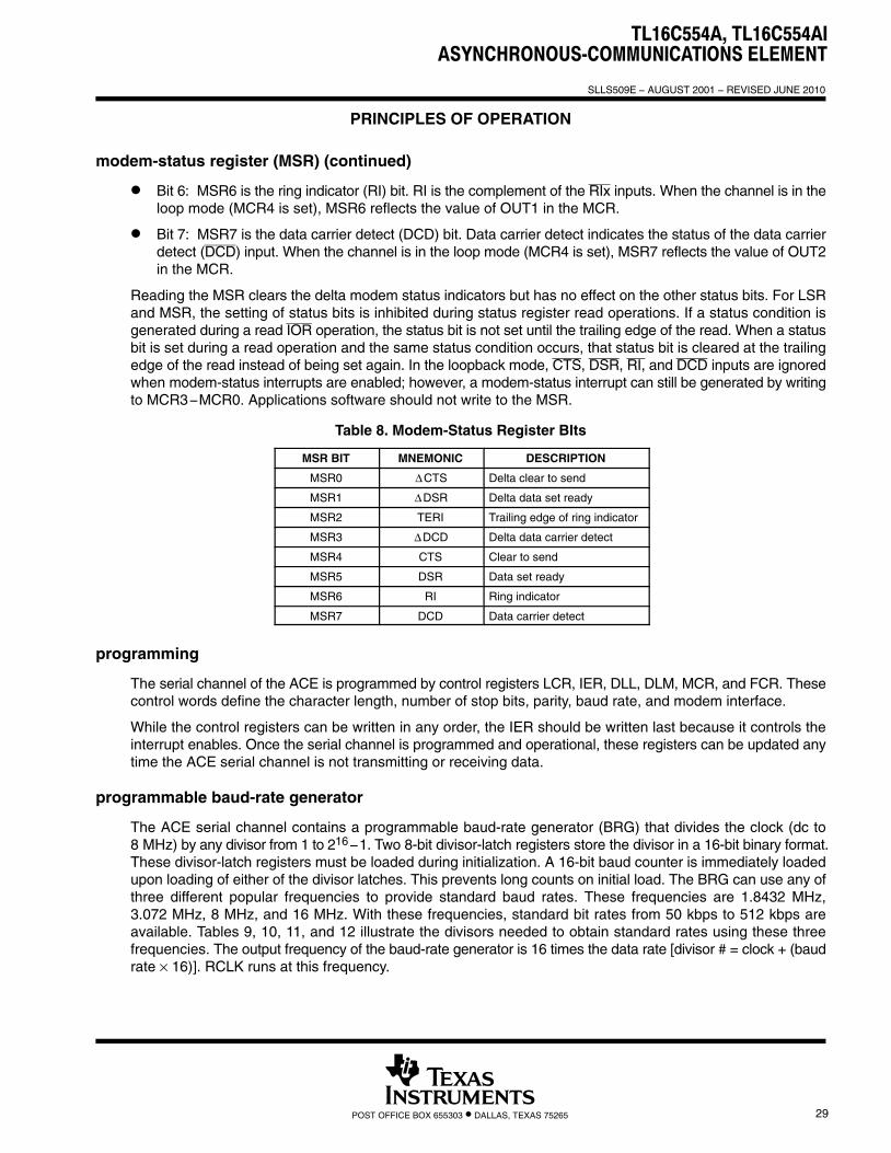
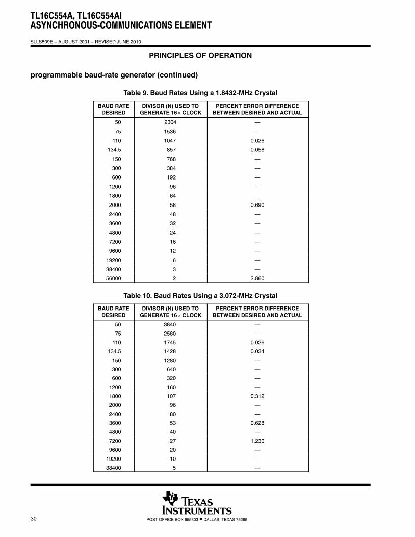
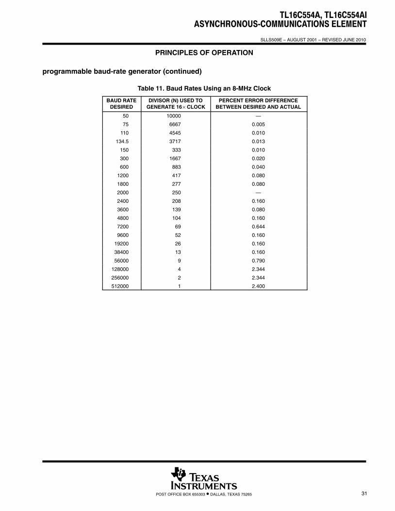
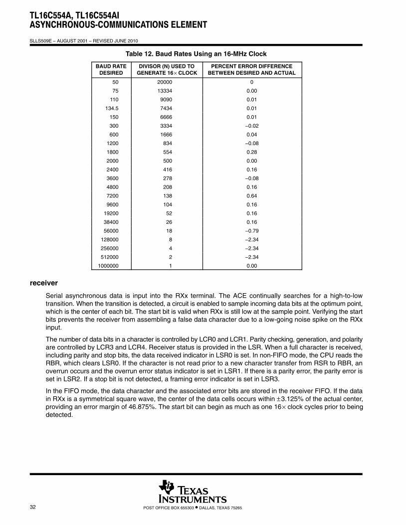
programmable baud-rate generator
The ACE serial channel contains a programmable baud-rate generator (BRG) that divides the clock (dc to8 MHz) by any divisor from 1 to 216−1. Two 8-bit divisor-latch registers store the divisor in a 16-bit binary format.These divisor-latch registers must be loaded during initialization. A 16-bit baud counter is immediately loadedupon loading of either of the divisor latches. This prevents long counts on initial load. The BRG can use any ofthree different popular frequencies to provide standard baud rates. These frequencies are 1.8432 MHz,3.072 MHz, 8 MHz, and 16 MHz. With these frequencies, standard bit rates from 50 kbps to 512 kbps areavailable. Tables 9, 10, 11, and 12 illustrate the divisors needed to obtain standard rates using these threefrequencies. The output frequency of the baud-rate generator is 16 times the data rate [divisor # = clock + (baudrate × 16)]. RCLK runs at this frequency.
TL16C554A, TL16C554AIASYNCHRONOUS-COMMUNICATIONS ELEMENT�
�
SLLS509E − AUGUST 2001 − REVISED JUNE 2010
30 POST OFFICE BOX 655303 • DALLAS, TEXAS 75265
PRINCIPLES OF OPERATION
programmable baud-rate generator (continued)
Table 9. Baud Rates Using a 1.8432-MHz Crystal
BAUD RATEDESIRED
DIVISOR (N) USED TOGENERATE 16× CLOCK
PERCENT ERROR DIFFERENCEBETWEEN DESIRED AND ACTUAL
50 2304 —
75 1536 —
110 1047 0.026
134.5 857 0.058
150 768 —
300 384 —
600 192 —
1200 96 —
1800 64 —
2000 58 0.690
2400 48 —
3600 32 —
4800 24 —
7200 16 —
9600 12 —
19200 6 —
38400 3 —
56000 2 2.860
Table 10. Baud Rates Using a 3.072-MHz Crystal
BAUD RATEDESIRED
DIVISOR (N) USED TOGENERATE 16× CLOCK
PERCENT ERROR DIFFERENCEBETWEEN DESIRED AND ACTUAL
50 3840 —
75 2560 —
110 1745 0.026
134.5 1428 0.034
150 1280 —
300 640 —
600 320 —
1200 160 —
1800 107 0.312
2000 96 —
2400 80 —
3600 53 0.628
4800 40 —
7200 27 1.230
9600 20 —
19200 10 —
38400 5 —
TL16C554A, TL16C554AIASYNCHRONOUS-COMMUNICATIONS ELEMENT
�
�
SLLS509E − AUGUST 2001 − REVISED JUNE 2010
31POST OFFICE BOX 655303 • DALLAS, TEXAS 75265
PRINCIPLES OF OPERATION
programmable baud-rate generator (continued)
Table 11. Baud Rates Using an 8-MHz Clock
BAUD RATEDESIRED
DIVISOR (N) USED TOGENERATE 16× CLOCK
PERCENT ERROR DIFFERENCEBETWEEN DESIRED AND ACTUAL
50 10000 —
75 6667 0.005
110 4545 0.010
134.5 3717 0.013
150 333 0.010
300 1667 0.020
600 883 0.040
1200 417 0.080
1800 277 0.080
2000 250 —
2400 208 0.160
3600 139 0.080
4800 104 0.160
7200 69 0.644
9600 52 0.160
19200 26 0.160
38400 13 0.160
56000 9 0.790
128000 4 2.344
256000 2 2.344
512000 1 2.400
TL16C554A, TL16C554AIASYNCHRONOUS-COMMUNICATIONS ELEMENT�
�
SLLS509E − AUGUST 2001 − REVISED JUNE 2010
32 POST OFFICE BOX 655303 • DALLAS, TEXAS 75265
Table 12. Baud Rates Using an 16-MHz Clock
BAUD RATEDESIRED
DIVISOR (N) USED TOGENERATE 16× CLOCK
PERCENT ERROR DIFFERENCEBETWEEN DESIRED AND ACTUAL
50 20000 0
75 13334 0.00
110 9090 0.01
134.5 7434 0.01
150 6666 0.01
300 3334 −0.02
600 1666 0.04
1200 834 −0.08
1800 554 0.28
2000 500 0.00
2400 416 0.16
3600 278 −0.08
4800 208 0.16
7200 138 0.64
9600 104 0.16
19200 52 0.16
38400 26 0.16
56000 18 −0.79
128000 8 −2.34
256000 4 −2.34
512000 2 −2.34
1000000 1 0.00
receiver
Serial asynchronous data is input into the RXx terminal. The ACE continually searches for a high-to-lowtransition. When the transition is detected, a circuit is enabled to sample incoming data bits at the optimum point,which is the center of each bit. The start bit is valid when RXx is still low at the sample point. Verifying the startbits prevents the receiver from assembling a false data character due to a low-going noise spike on the RXxinput.
The number of data bits in a character is controlled by LCR0 and LCR1. Parity checking, generation, and polarityare controlled by LCR3 and LCR4. Receiver status is provided in the LSR. When a full character is received,including parity and stop bits, the data received indicator in LSR0 is set. In non-FIFO mode, the CPU reads theRBR, which clears LSR0. If the character is not read prior to a new character transfer from RSR to RBR, anoverrun occurs and the overrun error status indicator is set in LSR1. If there is a parity error, the parity error isset in LSR2. If a stop bit is not detected, a framing error indicator is set in LSR3.
In the FIFO mode, the data character and the associated error bits are stored in the receiver FIFO. If the datain RXx is a symmetrical square wave, the center of the data cells occurs within ±3.125% of the actual center,providing an error margin of 46.875%. The start bit can begin as much as one 16× clock cycles prior to beingdetected.
TL16C554A, TL16C554AIASYNCHRONOUS-COMMUNICATIONS ELEMENT
�
�
SLLS509E − AUGUST 2001 − REVISED JUNE 2010
33POST OFFICE BOX 655303 • DALLAS, TEXAS 75265
PRINCIPLES OF OPERATION
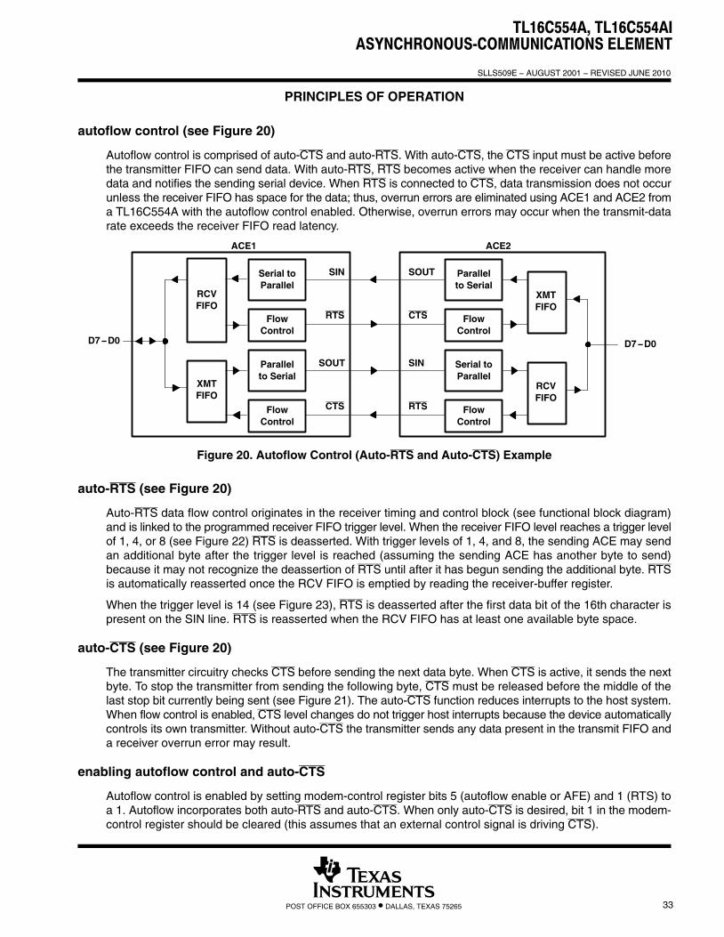
autoflow control (see Figure 20)
Autoflow control is comprised of auto-CTS and auto-RTS. With auto-CTS, the CTS input must be active beforethe transmitter FIFO can send data. With auto-RTS, RTS becomes active when the receiver can handle moredata and notifies the sending serial device. When RTS is connected to CTS, data transmission does not occurunless the receiver FIFO has space for the data; thus, overrun errors are eliminated using ACE1 and ACE2 froma TL16C554A with the autoflow control enabled. Otherwise, overrun errors may occur when the transmit-datarate exceeds the receiver FIFO read latency.
RCVFIFO
Serial toParallel
FlowControl
XMTFIFO
Parallelto Serial
FlowControl
Parallelto Serial
FlowControl
Serial toParallel
FlowControl
XMTFIFO
RCVFIFO
ACE1 ACE2
D7−D0
SIN SOUT
RTS CTS
SOUT SIN
CTS RTS
D7−D0
Figure 20. Autoflow Control (Auto-RTS and Auto-CTS) Example
auto-RTS (see Figure 20)
Auto-RTS data flow control originates in the receiver timing and control block (see functional block diagram)and is linked to the programmed receiver FIFO trigger level. When the receiver FIFO level reaches a trigger levelof 1, 4, or 8 (see Figure 22) RTS is deasserted. With trigger levels of 1, 4, and 8, the sending ACE may sendan additional byte after the trigger level is reached (assuming the sending ACE has another byte to send)because it may not recognize the deassertion of RTS until after it has begun sending the additional byte. RTSis automatically reasserted once the RCV FIFO is emptied by reading the receiver-buffer register.
When the trigger level is 14 (see Figure 23), RTS is deasserted after the first data bit of the 16th character ispresent on the SIN line. RTS is reasserted when the RCV FIFO has at least one available byte space.
auto-CTS (see Figure 20)
The transmitter circuitry checks CTS before sending the next data byte. When CTS is active, it sends the nextbyte. To stop the transmitter from sending the following byte, CTS must be released before the middle of thelast stop bit currently being sent (see Figure 21). The auto-CTS function reduces interrupts to the host system.When flow control is enabled, CTS level changes do not trigger host interrupts because the device automaticallycontrols its own transmitter. Without auto-CTS the transmitter sends any data present in the transmit FIFO anda receiver overrun error may result.
enabling autoflow control and auto-CTS
Autoflow control is enabled by setting modem-control register bits 5 (autoflow enable or AFE) and 1 (RTS) toa 1. Autoflow incorporates both auto-RTS and auto-CTS. When only auto-CTS is desired, bit 1 in the modem-control register should be cleared (this assumes that an external control signal is driving CTS).
TL16C554A, TL16C554AIASYNCHRONOUS-COMMUNICATIONS ELEMENT�
�
SLLS509E − AUGUST 2001 − REVISED JUNE 2010
34 POST OFFICE BOX 655303 • DALLAS, TEXAS 75265
PRINCIPLES OF OPERATION
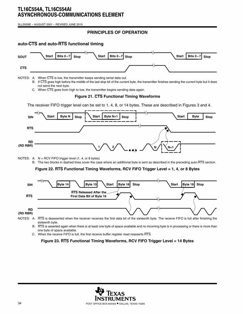
auto-CTS and auto-RTS functional timing
Start Bits 0−7 Start Bits 0−7 Start Bits 0−7Stop Stop StopSOUT
CTS
NOTES: A. When CTS is low, the transmitter keeps sending serial data out.B. If CTS goes high before the middle of the last stop bit of the current byte, the transmitter finishes sending the current byte but it does
not send the next byte.C. When CTS goes from high to low, the transmitter begins sending data again.
Figure 21. CTS Functional Timing Waveforms
The receiver FIFO trigger level can be set to 1, 4, 8, or 14 bytes. These are described in Figures 3 and 4.
Start Byte N Start Byte N+1 Start ByteStop Stop StopSIN
RTS
RD(RD RBR) 1 2 N N+1
NOTES: A. N = RCV FIFO trigger level (1, 4, or 8 bytes)B. The two blocks in dashed lines cover the case where an additional byte is sent as described in the preceding auto-RTS section.
Figure 22. RTS Functional Timing Waveforms, RCV FIFO Trigger Level = 1, 4, or 8 Bytes
Byte 14 Byte 15SIN
RTS
RD(RD RBR)
Start Byte 18 StopStart Byte 16 Stop
RTS Released After theFirst Data Bit of Byte 16
NOTES: A. RTS is deasserted when the receiver receives the first data bit of the sixteenth byte. The receive FIFO is full after finishing thesixteenth byte.
B. RTS is asserted again when there is at least one byte of space available and no incoming byte is in processing or there is more thanone byte of space available.
C. When the receive FIFO is full, the first receive buffer register read reasserts RTS.
Figure 23. RTS Functional Timing Waveforms, RCV FIFO Trigger Level = 14 Bytes
TL16C554A, TL16C554AIASYNCHRONOUS-COMMUNICATIONS ELEMENT
�
�
SLLS509E − AUGUST 2001 − REVISED JUNE 2010
35POST OFFICE BOX 655303 • DALLAS, TEXAS 75265
PRINCIPLES OF OPERATION
reset
After power up, the ACE RESET input should be held high for one microsecond to reset the ACE circuits to anidle mode until initialization. A high on RESET causes the following:
1. Initializes the transmitter and receiver internal clock counters.
2. Clears the LSR, except for transmitter register empty (TEMT) and transmit holding register empty (THRE),which are set. The MCR is also cleared. All of the discrete lines, memory elements, and miscellaneous logicassociated with these register bits are also cleared or turned off. The LCR, divisor latches, RBR, andtransmitter-buffer register are not affected.
RXRDY operation
In mode 0, RXRDY is asserted (low) when the receive FIFO is not empty; it is released (high) when the FIFOis empty. In this way, the receiver FIFO is read when RXRDY is asserted (low).
In mode 1, RXRDY is asserted (low) when the receive FIFO has filled to the trigger level or a character time-outhas occurred (four character times with no transmission of characters); it is released (high) when the FIFO isempty. In this mode, many received characters are read by the DMA device, reducing the number of times itis interrupted.
RXRDY and TXRDY outputs from each of the four internal ACEs of the TL16C554A are ANDed togetherinternally. This combined signal is brought out externally to RXRDY and TXRDY.
Following the removal of the reset condition (RESET low), the ACE remains in the idle mode until programmed.A hardware reset of the ACE sets the THRE and TEMT status bits in the LSR. When interrupts are subsequentlyenabled, an interrupt occurs due to THRE. A summary of the effect of a reset on the ACE is given in Table 13.
Table 13. RESET Effects on Registers and Signals
REGISTER/SIGNAL RESET CONTROL RESET STATE
Interrupt-enable register Reset All bits cleared (0−3 forced and 4−7 permanent)
Interrupt-identification register ResetBit 0 is set, bits 1, 2, 3, 6, and 7 are cleared,Bits 4−5 are permanently cleared
Line-control register Reset All bits cleared
Modem-control register Reset All bits cleared (5−7 permanent)
FIFO-control register Reset All bits cleared
Line-status register Reset All bits cleared, except bits 5 and 6 are set
Modem-status register Reset Bits 0−3 cleared, bits 4−7 input signals
TXx Reset High
Interrupt (RCVR ERRS) Read LSR/reset Low
Interrupt (receiver data ready) Read RBR/reset Low
Interrupt (THRE) Read IIR/write THR/reset Low
Interrupt (modem status changes) Read MSR/reset Low
RTS Reset High
DTR Reset High
TL16C554A, TL16C554AIASYNCHRONOUS-COMMUNICATIONS ELEMENT�
�
SLLS509E − AUGUST 2001 − REVISED JUNE 2010
36 POST OFFICE BOX 655303 • DALLAS, TEXAS 75265
PRINCIPLES OF OPERATION
scratchpad register
The scratchpad register is an 8-bit read/write register that has no effect on any ACE channel. It is intended tobe used by the programmer to hold data temporarily.
TXRDY operation
In mode 0, TXRDY is asserted (low) when the transmit FIFO is empty; it is released (high) when the FIFOcontains at least one byte. In this way, the FIFO is written with 16 bytes when TXRDY is asserted (low).
In mode 1, TXRDY is asserted (low) when the transmit FIFO is not full; in this mode, the transmit FIFO is writtenwith another byte when TXRDY is asserted (low).
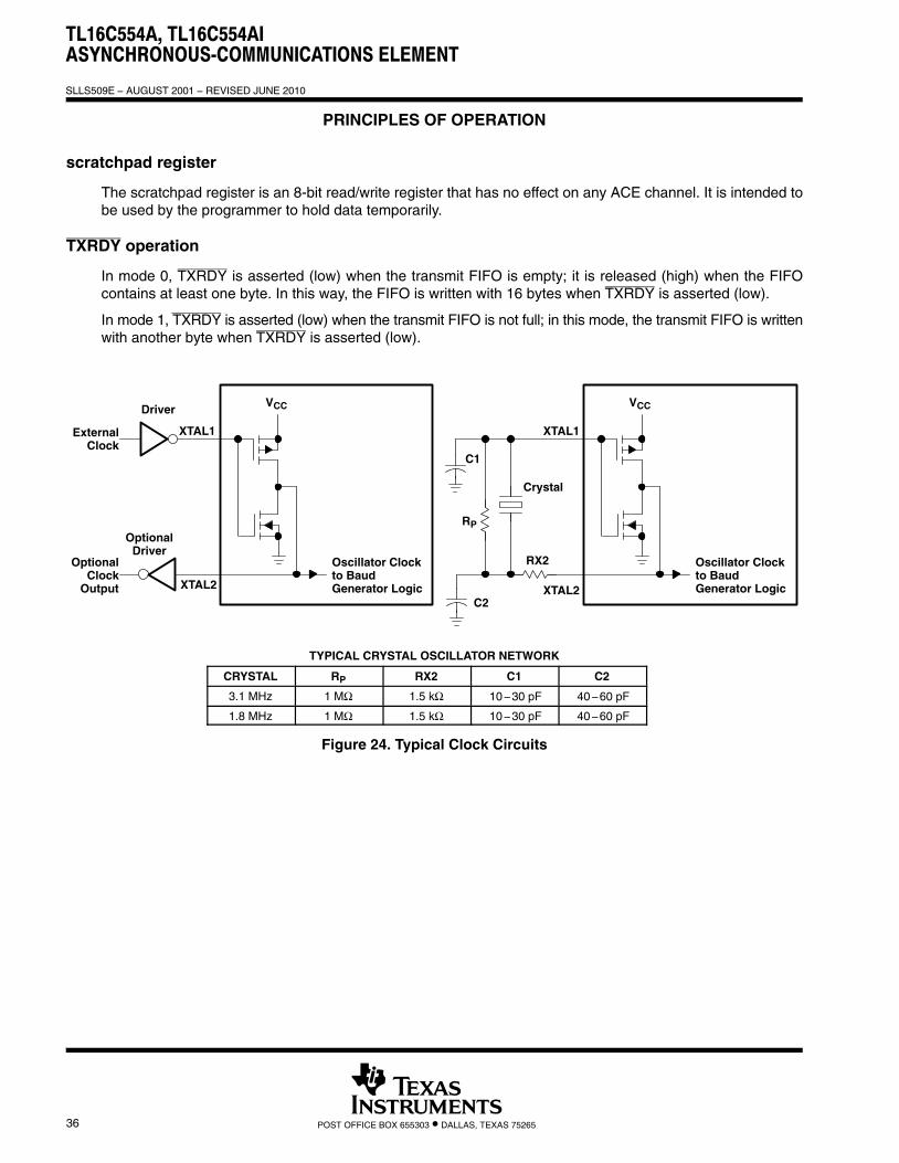
Driver
OptionalDriver
ExternalClock
OptionalClock
Output
Oscillator Clockto Baud Generator Logic
VCC
Crystal
Oscillator Clockto Baud Generator Logic
RX2
VCC
C1
RP
C2
XTAL1 XTAL1
XTAL2 XTAL2
TYPICAL CRYSTAL OSCILLATOR NETWORK
CRYSTAL RP RX2 C1 C2
3.1 MHz 1 MΩ 1.5 kΩ 10�−�30 pF 40�−�60 pF
1.8 MHz 1 MΩ 1.5 kΩ 10−30 pF 40−60 pF
Figure 24. Typical Clock Circuits
TL16C554A, TL16C554AIASYNCHRONOUS-COMMUNICATIONS ELEMENT
�
�
SLLS509E − AUGUST 2001 − REVISED JUNE 2010
37POST OFFICE BOX 655303 • DALLAS, TEXAS 75265
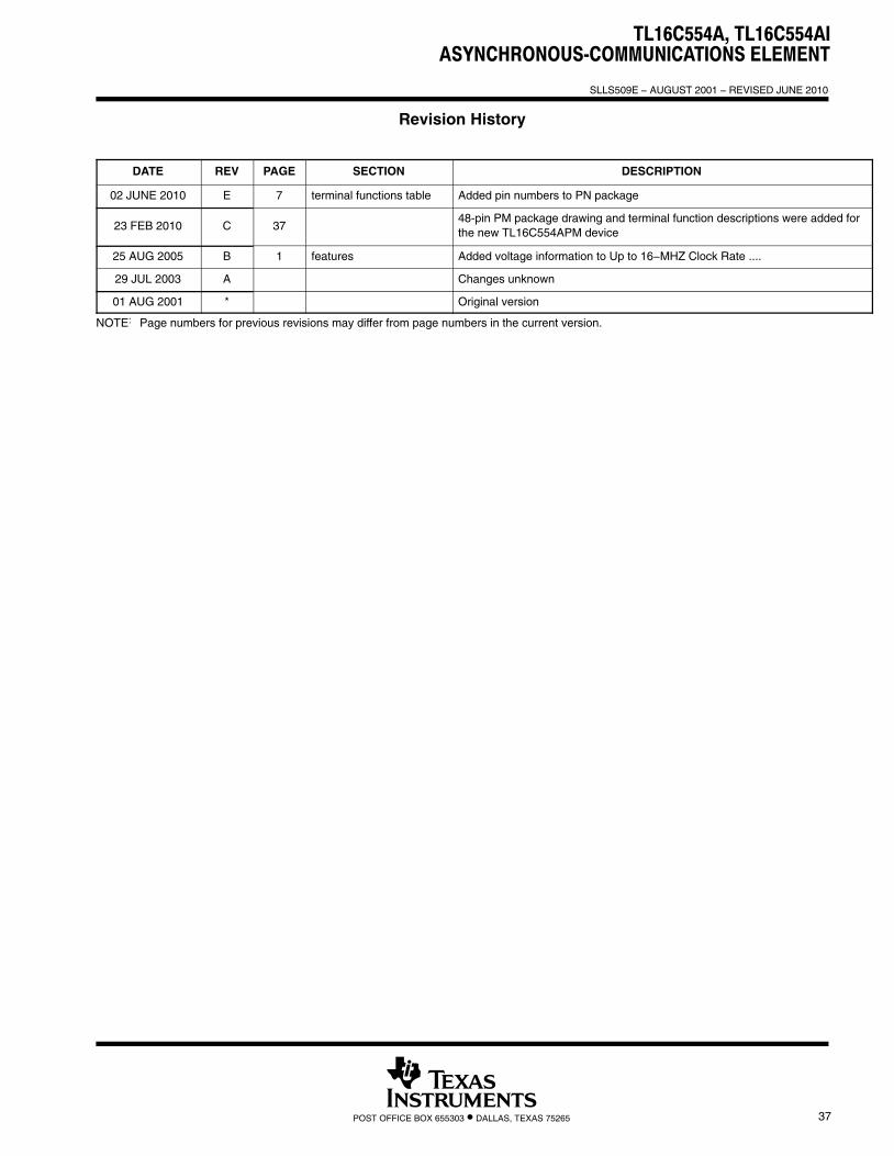
Revision History
DATE REV PAGE SECTION DESCRIPTION
02 JUNE 2010 E 7 terminal functions table Added pin numbers to PN package
23 FEB 2010 C 3748-pin PM package drawing and terminal function descriptions were added forthe new TL16C554APM device
25 AUG 2005 B 1 features Added voltage information to Up to 16−MHZ Clock Rate ....
29 JUL 2003 A Changes unknown
01 AUG 2001 * Original version
NOTE: Page numbers for previous revisions may differ from page numbers in the current version.
TL16C554A, TL16C554AIASYNCHRONOUS-COMMUNICATIONS ELEMENT�
�
SLLS509E − AUGUST 2001 − REVISED JUNE 2010
38 POST OFFICE BOX 655303 • DALLAS, TEXAS 75265
Revision History
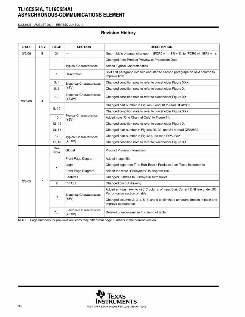
DATE REV PAGE SECTION DESCRIPTION
3/2/06 B 21 — Near middle of page, changed (FCR0 = 1, IER = 1). to (FCR0 =1, IER1 = 1).
— — Changed from Product Preview to Production Data.
— Typical Characteristics Added Typical Characteristics.
1 DescriptionSplit first paragraph into two and started second paragraph on next column toimprove flow.
3, 4 Electrical Characteristics Changed condition note to refer to placeholder Figure XXX.
5, 6
Electrical Characteristics(+5V) Changed condition note to refer to placeholder Figure X.
2/25/05 A7, 8
Electrical Characteristics(+3.3V)
Changed condition note to refer to placeholder Figure XX.2/25/05 A
9 10Changed part number in Figures 6 and 10 to read OPA2832.
9, 10
T i l Ch t i tiChanged condition note to refer to placeholder Figure XXX.
10Typical Characteristics(+5V)
Added note “One Channel Only” to Figure 11.
12−15(+5V)
Changed condition note to refer to placeholder Figure X.
13, 14 Changed part number in Figures 29, 32, and 34 to read OPA2832.
17 Typical Characteristics Changed part number in Figure 49 to read OPA2832.
17, 18
Typical Characteristics(+3.3V) Changed condition note to refer to placeholder Figure XX.
SeeNote
Global Product Preview information.
Front Page Diagram Added image title.
1Logo Changed logo from TI to Burr-Brown Products from Texas Instruments
1Front Page Diagram Added the word “Chebyshev” to diagram title.
2/8/05 *Features Changed 350V/ns to 350V/μs in sixth bullet.
2/8/05 *2 Pin Out Changed pin out drawing.
3Electrical Characteristics
Added em-dash (—) to +25°C column of Input Bias Current Drift line under DCPerformance section of table.
3Electrical Characteristics(±5V) Changed columns 2, 3, 4, 5, 7, and 9 to eliminate unnatural breaks in table and
improve appearance.
7, 8Electrical Characteristics(+3.3V)
Deleted unnecessary sixth column of table.
NOTE: Page numbers for previous revisions may differ from page numbers in the current version.
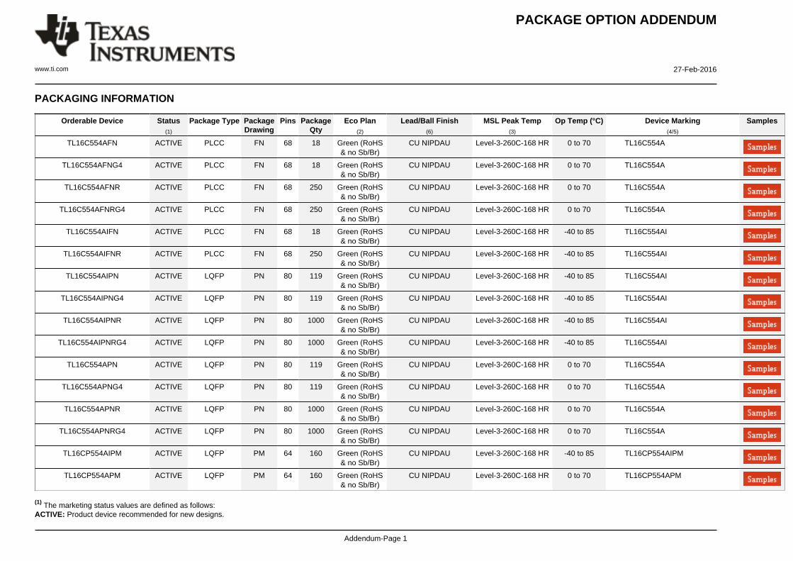
PACKAGE OPTION ADDENDUM
www.ti.com 27-Feb-2016
Addendum-Page 1
PACKAGING INFORMATION
Orderable Device Status(1)
Package Type PackageDrawing
Pins PackageQty
Eco Plan(2)
Lead/Ball Finish(6)
MSL Peak Temp(3)
Op Temp (°C) Device Marking(4/5)
Samples
TL16C554AFN ACTIVE PLCC FN 68 18 Green (RoHS& no Sb/Br)
CU NIPDAU Level-3-260C-168 HR 0 to 70 TL16C554A
TL16C554AFNG4 ACTIVE PLCC FN 68 18 Green (RoHS& no Sb/Br)
CU NIPDAU Level-3-260C-168 HR 0 to 70 TL16C554A
TL16C554AFNR ACTIVE PLCC FN 68 250 Green (RoHS& no Sb/Br)
CU NIPDAU Level-3-260C-168 HR 0 to 70 TL16C554A
TL16C554AFNRG4 ACTIVE PLCC FN 68 250 Green (RoHS& no Sb/Br)
CU NIPDAU Level-3-260C-168 HR 0 to 70 TL16C554A
TL16C554AIFN ACTIVE PLCC FN 68 18 Green (RoHS& no Sb/Br)
CU NIPDAU Level-3-260C-168 HR -40 to 85 TL16C554AI
TL16C554AIFNR ACTIVE PLCC FN 68 250 Green (RoHS& no Sb/Br)
CU NIPDAU Level-3-260C-168 HR -40 to 85 TL16C554AI
TL16C554AIPN ACTIVE LQFP PN 80 119 Green (RoHS& no Sb/Br)
CU NIPDAU Level-3-260C-168 HR -40 to 85 TL16C554AI
TL16C554AIPNG4 ACTIVE LQFP PN 80 119 Green (RoHS& no Sb/Br)
CU NIPDAU Level-3-260C-168 HR -40 to 85 TL16C554AI
TL16C554AIPNR ACTIVE LQFP PN 80 1000 Green (RoHS& no Sb/Br)
CU NIPDAU Level-3-260C-168 HR -40 to 85 TL16C554AI
TL16C554AIPNRG4 ACTIVE LQFP PN 80 1000 Green (RoHS& no Sb/Br)
CU NIPDAU Level-3-260C-168 HR -40 to 85 TL16C554AI
TL16C554APN ACTIVE LQFP PN 80 119 Green (RoHS& no Sb/Br)
CU NIPDAU Level-3-260C-168 HR 0 to 70 TL16C554A
TL16C554APNG4 ACTIVE LQFP PN 80 119 Green (RoHS& no Sb/Br)
CU NIPDAU Level-3-260C-168 HR 0 to 70 TL16C554A
TL16C554APNR ACTIVE LQFP PN 80 1000 Green (RoHS& no Sb/Br)
CU NIPDAU Level-3-260C-168 HR 0 to 70 TL16C554A
TL16C554APNRG4 ACTIVE LQFP PN 80 1000 Green (RoHS& no Sb/Br)
CU NIPDAU Level-3-260C-168 HR 0 to 70 TL16C554A
TL16CP554AIPM ACTIVE LQFP PM 64 160 Green (RoHS& no Sb/Br)
CU NIPDAU Level-3-260C-168 HR -40 to 85 TL16CP554AIPM
TL16CP554APM ACTIVE LQFP PM 64 160 Green (RoHS& no Sb/Br)
CU NIPDAU Level-3-260C-168 HR 0 to 70 TL16CP554APM
(1) The marketing status values are defined as follows:ACTIVE: Product device recommended for new designs.
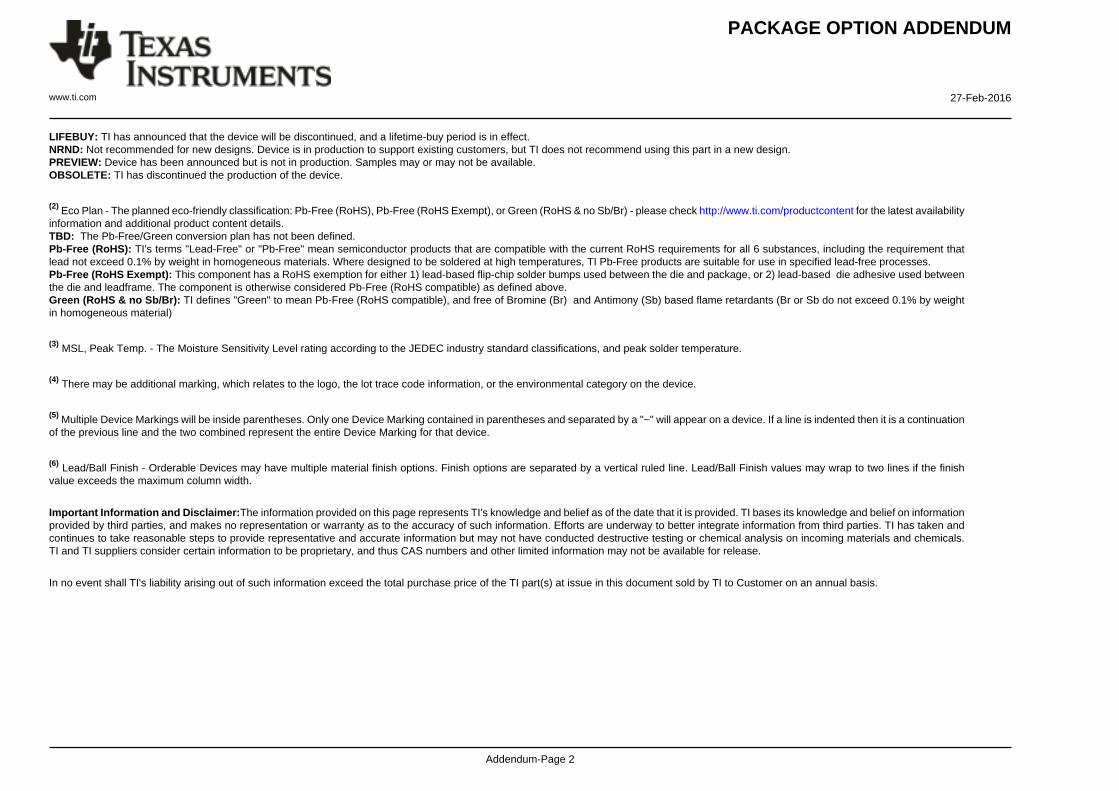
PACKAGE OPTION ADDENDUM
www.ti.com 27-Feb-2016
Addendum-Page 2
LIFEBUY: TI has announced that the device will be discontinued, and a lifetime-buy period is in effect.NRND: Not recommended for new designs. Device is in production to support existing customers, but TI does not recommend using this part in a new design.PREVIEW: Device has been announced but is not in production. Samples may or may not be available.OBSOLETE: TI has discontinued the production of the device.
(2) Eco Plan - The planned eco-friendly classification: Pb-Free (RoHS), Pb-Free (RoHS Exempt), or Green (RoHS & no Sb/Br) - please check http://www.ti.com/productcontent for the latest availabilityinformation and additional product content details.TBD: The Pb-Free/Green conversion plan has not been defined.Pb-Free (RoHS): TI's terms "Lead-Free" or "Pb-Free" mean semiconductor products that are compatible with the current RoHS requirements for all 6 substances, including the requirement thatlead not exceed 0.1% by weight in homogeneous materials. Where designed to be soldered at high temperatures, TI Pb-Free products are suitable for use in specified lead-free processes.Pb-Free (RoHS Exempt): This component has a RoHS exemption for either 1) lead-based flip-chip solder bumps used between the die and package, or 2) lead-based die adhesive used betweenthe die and leadframe. The component is otherwise considered Pb-Free (RoHS compatible) as defined above.Green (RoHS & no Sb/Br): TI defines "Green" to mean Pb-Free (RoHS compatible), and free of Bromine (Br) and Antimony (Sb) based flame retardants (Br or Sb do not exceed 0.1% by weightin homogeneous material)
(3) MSL, Peak Temp. - The Moisture Sensitivity Level rating according to the JEDEC industry standard classifications, and peak solder temperature.
(4) There may be additional marking, which relates to the logo, the lot trace code information, or the environmental category on the device.
(5) Multiple Device Markings will be inside parentheses. Only one Device Marking contained in parentheses and separated by a "~" will appear on a device. If a line is indented then it is a continuationof the previous line and the two combined represent the entire Device Marking for that device.
(6) Lead/Ball Finish - Orderable Devices may have multiple material finish options. Finish options are separated by a vertical ruled line. Lead/Ball Finish values may wrap to two lines if the finishvalue exceeds the maximum column width.
Important Information and Disclaimer:The information provided on this page represents TI's knowledge and belief as of the date that it is provided. TI bases its knowledge and belief on informationprovided by third parties, and makes no representation or warranty as to the accuracy of such information. Efforts are underway to better integrate information from third parties. TI has taken andcontinues to take reasonable steps to provide representative and accurate information but may not have conducted destructive testing or chemical analysis on incoming materials and chemicals.TI and TI suppliers consider certain information to be proprietary, and thus CAS numbers and other limited information may not be available for release.
In no event shall TI's liability arising out of such information exceed the total purchase price of the TI part(s) at issue in this document sold by TI to Customer on an annual basis.
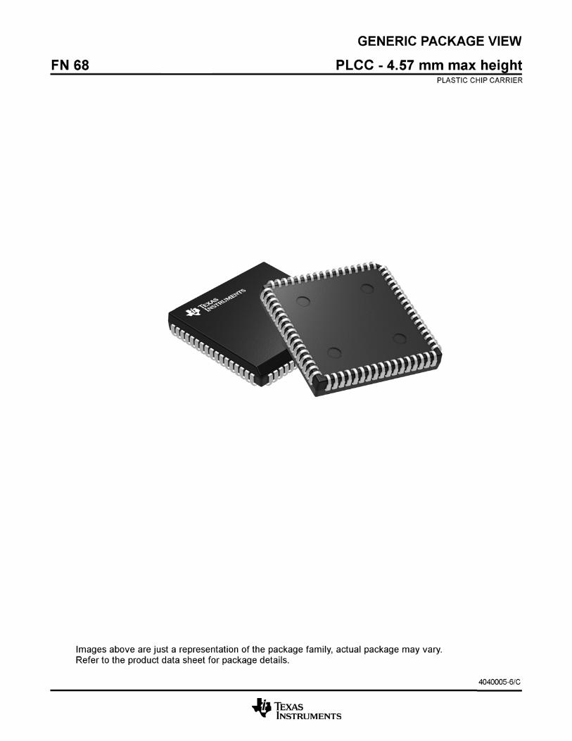
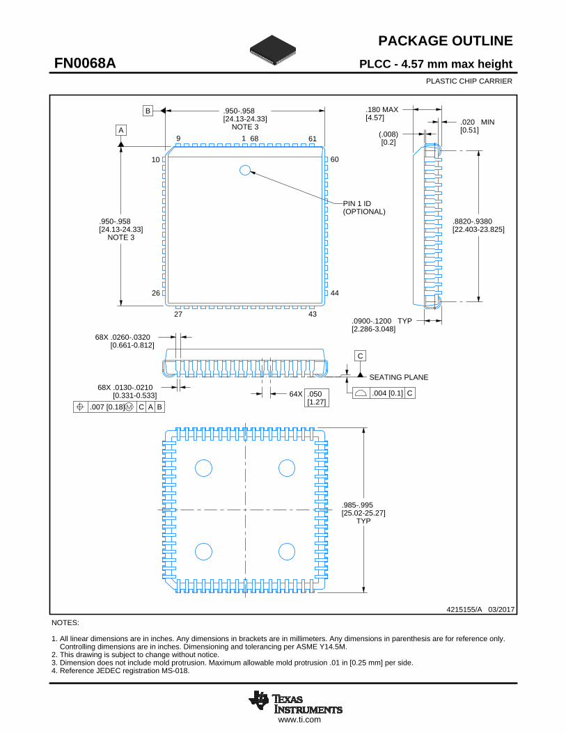
www.ti.com
PACKAGE OUTLINE
C
68X -.0210.0130-0.5330.331[ ]
68X -.0320.0260-0.8120.661[ ]
TYP
-.995.985-25.2725.02[ ]
64X .050[1.27]
-.9380.8820-23.82522.403[ ]
.020 MIN[0.51]
TYP-.1200.0900-3.0482.286[ ]
.180 MAX[4.57]
B
NOTE 3
-.958.950-24.3324.13[ ]
A
NOTE 3
-.958.950-24.3324.13[ ]
(.008)[0.2]
4215155/A 03/2017
4215155/A 03/2017
PLCC - 4.57 mm max heightFN0068APLASTIC CHIP CARRIER
SEATING PLANEPLANE
NOTES: 1. All linear dimensions are in inches. Any dimensions in brackets are in millimeters. Any dimensions in parenthesis are for reference only. Controlling dimensions are in inches. Dimensioning and tolerancing per ASME Y14.5M. 2. This drawing is subject to change without notice.3. Dimension does not include mold protrusion. Maximum allowable mold protrusion .01 in [0.25 mm] per side.4. Reference JEDEC registration MS-018.
PIN 1 ID(OPTIONAL)
1 689
27 43
44
60
61
10
26
.004 [0.1] C
.007 [0.18] C A B
SCALE 0.530
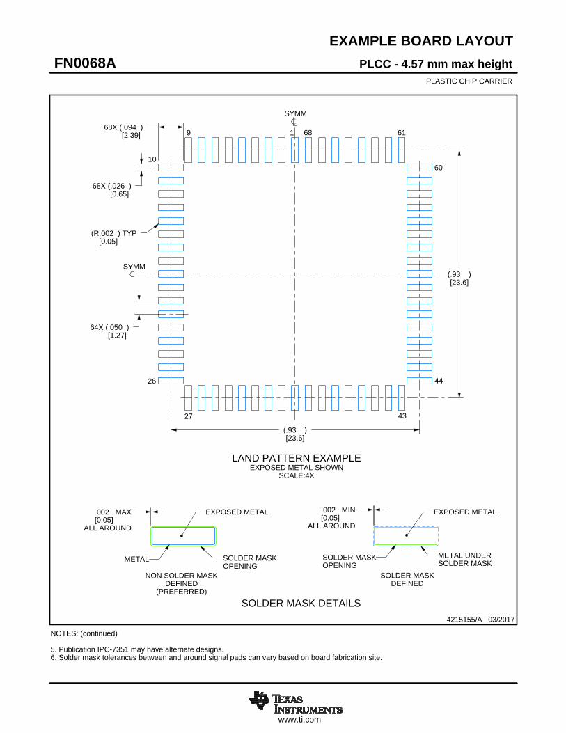
www.ti.com
EXAMPLE BOARD LAYOUT
.002 MAX[0.05]
ALL AROUND
.002 MIN[0.05]
ALL AROUND
68X (.094 )[2.39]
68X (.026 )[0.65]
64X (.050 )[1.27]
(.93 )[23.6]
(.93 )[23.6]
(R.002 ) TYP[0.05]
4215155/A 03/2017
4215155/A 03/2017
PLCC - 4.57 mm max heightFN0068APLASTIC CHIP CARRIER
NOTES: (continued) 5. Publication IPC-7351 may have alternate designs.6. Solder mask tolerances between and around signal pads can vary based on board fabrication site.
LAND PATTERN EXAMPLEEXPOSED METAL SHOWN
SCALE:4X
SYMM
SYMM
1 689
27 43
44
60
61
10
26
METAL SOLDER MASKOPENING
NON SOLDER MASKDEFINED
(PREFERRED)
SOLDER MASK DETAILS
EXPOSED METAL
SOLDER MASKOPENING
METAL UNDERSOLDER MASK
SOLDER MASKDEFINED
EXPOSED METAL
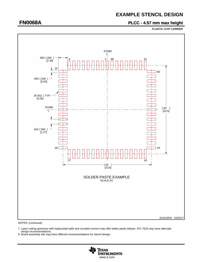
www.ti.com
EXAMPLE STENCIL DESIGN
68X (.026 )[0.65]
68X (.094 )[2.39]
(.93 )[23.6]
(.93 )[23.6]
64X (.050 )[1.27]
(R.002 ) TYP[0.05]
PLCC - 4.57 mm max heightFN0068APLASTIC CHIP CARRIER
4215155/A 03/2017
PLCC - 4.57 mm max heightFN0068APLASTIC CHIP CARRIER
NOTES: (continued) 7. Laser cutting apertures with trapezoidal walls and rounded corners may offer better paste release. IPC-7525 may have alternate design recommendations.8. Board assembly site may have different recommendations for stencil design.
SYMM
SYMM
1 689
27 43
44
60
61
10
26
SOLDER PASTE EXAMPLESCALE:4X
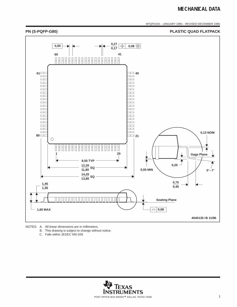
MECHANICAL DATA
MTQF010A – JANUARY 1995 – REVISED DECEMBER 1996
1POST OFFICE BOX 655303 • DALLAS, TEXAS 75265
PN (S-PQFP-G80) PLASTIC QUAD FLATPACK
4040135 /B 11/96
0,170,27
0,13 NOM
40
21
0,25
0,450,75
0,05 MIN
Seating Plane
Gage Plane
4160
61
80
20
SQ
SQ
1
13,8014,20
12,20
9,50 TYP
11,80
1,451,35
1,60 MAX 0,08
0,50 M0,08
0°–7°
NOTES: A. All linear dimensions are in millimeters.B. This drawing is subject to change without notice.C. Falls within JEDEC MS-026
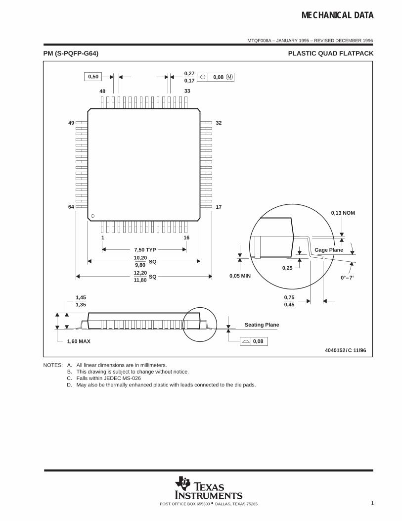
MECHANICAL DATA
MTQF008A – JANUARY 1995 – REVISED DECEMBER 1996
1POST OFFICE BOX 655303 • DALLAS, TEXAS 75265
PM (S-PQFP-G64) PLASTIC QUAD FLATPACK
4040152/C 11/96
32
170,13 NOM
0,25
0,450,75
Seating Plane
0,05 MIN
Gage Plane
0,27
33
16
48
1
0,17
49
64
SQ
SQ10,20
11,8012,20
9,80
7,50 TYP
1,60 MAX
1,451,35
0,08
0,50 M0,08
0°–7°
NOTES: A. All linear dimensions are in millimeters.B. This drawing is subject to change without notice.C. Falls within JEDEC MS-026D. May also be thermally enhanced plastic with leads connected to the die pads.

IMPORTANT NOTICE
Texas Instruments Incorporated (TI) reserves the right to make corrections, enhancements, improvements and other changes to itssemiconductor products and services per JESD46, latest issue, and to discontinue any product or service per JESD48, latest issue. Buyersshould obtain the latest relevant information before placing orders and should verify that such information is current and complete.TI’s published terms of sale for semiconductor products (http://www.ti.com/sc/docs/stdterms.htm) apply to the sale of packaged integratedcircuit products that TI has qualified and released to market. Additional terms may apply to the use or sale of other types of TI products andservices.Reproduction of significant portions of TI information in TI data sheets is permissible only if reproduction is without alteration and isaccompanied by all associated warranties, conditions, limitations, and notices. TI is not responsible or liable for such reproduceddocumentation. Information of third parties may be subject to additional restrictions. Resale of TI products or services with statementsdifferent from or beyond the parameters stated by TI for that product or service voids all express and any implied warranties for theassociated TI product or service and is an unfair and deceptive business practice. TI is not responsible or liable for any such statements.Buyers and others who are developing systems that incorporate TI products (collectively, “Designers”) understand and agree that Designersremain responsible for using their independent analysis, evaluation and judgment in designing their applications and that Designers havefull and exclusive responsibility to assure the safety of Designers' applications and compliance of their applications (and of all TI productsused in or for Designers’ applications) with all applicable regulations, laws and other applicable requirements. Designer represents that, withrespect to their applications, Designer has all the necessary expertise to create and implement safeguards that (1) anticipate dangerousconsequences of failures, (2) monitor failures and their consequences, and (3) lessen the likelihood of failures that might cause harm andtake appropriate actions. Designer agrees that prior to using or distributing any applications that include TI products, Designer willthoroughly test such applications and the functionality of such TI products as used in such applications.TI’s provision of technical, application or other design advice, quality characterization, reliability data or other services or information,including, but not limited to, reference designs and materials relating to evaluation modules, (collectively, “TI Resources”) are intended toassist designers who are developing applications that incorporate TI products; by downloading, accessing or using TI Resources in anyway, Designer (individually or, if Designer is acting on behalf of a company, Designer’s company) agrees to use any particular TI Resourcesolely for this purpose and subject to the terms of this Notice.TI’s provision of TI Resources does not expand or otherwise alter TI’s applicable published warranties or warranty disclaimers for TIproducts, and no additional obligations or liabilities arise from TI providing such TI Resources. TI reserves the right to make corrections,enhancements, improvements and other changes to its TI Resources. TI has not conducted any testing other than that specificallydescribed in the published documentation for a particular TI Resource.Designer is authorized to use, copy and modify any individual TI Resource only in connection with the development of applications thatinclude the TI product(s) identified in such TI Resource. NO OTHER LICENSE, EXPRESS OR IMPLIED, BY ESTOPPEL OR OTHERWISETO ANY OTHER TI INTELLECTUAL PROPERTY RIGHT, AND NO LICENSE TO ANY TECHNOLOGY OR INTELLECTUAL PROPERTYRIGHT OF TI OR ANY THIRD PARTY IS GRANTED HEREIN, including but not limited to any patent right, copyright, mask work right, orother intellectual property right relating to any combination, machine, or process in which TI products or services are used. Informationregarding or referencing third-party products or services does not constitute a license to use such products or services, or a warranty orendorsement thereof. Use of TI Resources may require a license from a third party under the patents or other intellectual property of thethird party, or a license from TI under the patents or other intellectual property of TI.TI RESOURCES ARE PROVIDED “AS IS” AND WITH ALL FAULTS. TI DISCLAIMS ALL OTHER WARRANTIES ORREPRESENTATIONS, EXPRESS OR IMPLIED, REGARDING RESOURCES OR USE THEREOF, INCLUDING BUT NOT LIMITED TOACCURACY OR COMPLETENESS, TITLE, ANY EPIDEMIC FAILURE WARRANTY AND ANY IMPLIED WARRANTIES OFMERCHANTABILITY, FITNESS FOR A PARTICULAR PURPOSE, AND NON-INFRINGEMENT OF ANY THIRD PARTY INTELLECTUALPROPERTY RIGHTS. TI SHALL NOT BE LIABLE FOR AND SHALL NOT DEFEND OR INDEMNIFY DESIGNER AGAINST ANY CLAIM,INCLUDING BUT NOT LIMITED TO ANY INFRINGEMENT CLAIM THAT RELATES TO OR IS BASED ON ANY COMBINATION OFPRODUCTS EVEN IF DESCRIBED IN TI RESOURCES OR OTHERWISE. IN NO EVENT SHALL TI BE LIABLE FOR ANY ACTUAL,DIRECT, SPECIAL, COLLATERAL, INDIRECT, PUNITIVE, INCIDENTAL, CONSEQUENTIAL OR EXEMPLARY DAMAGES INCONNECTION WITH OR ARISING OUT OF TI RESOURCES OR USE THEREOF, AND REGARDLESS OF WHETHER TI HAS BEENADVISED OF THE POSSIBILITY OF SUCH DAMAGES.Unless TI has explicitly designated an individual product as meeting the requirements of a particular industry standard (e.g., ISO/TS 16949and ISO 26262), TI is not responsible for any failure to meet such industry standard requirements.Where TI specifically promotes products as facilitating functional safety or as compliant with industry functional safety standards, suchproducts are intended to help enable customers to design and create their own applications that meet applicable functional safety standardsand requirements. Using products in an application does not by itself establish any safety features in the application. Designers mustensure compliance with safety-related requirements and standards applicable to their applications. Designer may not use any TI products inlife-critical medical equipment unless authorized officers of the parties have executed a special contract specifically governing such use.Life-critical medical equipment is medical equipment where failure of such equipment would cause serious bodily injury or death (e.g., lifesupport, pacemakers, defibrillators, heart pumps, neurostimulators, and implantables). Such equipment includes, without limitation, allmedical devices identified by the U.S. Food and Drug Administration as Class III devices and equivalent classifications outside the U.S.TI may expressly designate certain products as completing a particular qualification (e.g., Q100, Military Grade, or Enhanced Product).Designers agree that it has the necessary expertise to select the product with the appropriate qualification designation for their applicationsand that proper product selection is at Designers’ own risk. Designers are solely responsible for compliance with all legal and regulatoryrequirements in connection with such selection.Designer will fully indemnify TI and its representatives against any damages, costs, losses, and/or liabilities arising out of Designer’s non-compliance with the terms and provisions of this Notice.
Mailing Address: Texas Instruments, Post Office Box 655303, Dallas, Texas 75265Copyright © 2017, Texas Instruments Incorporated