Embed Size (px)
Citation preview

0.00
0.10
0.20
0.30
0.40
0.50
0.60
0.70
0.80
Frequency (Hz)
100 10k 100k1k
Ou
tpu
t S
pectr
al
No
ise
Den
sit
y (
µV
ÖH
z)
IOUT = 1 mA
IOUT = 1.5 A
VIN = 5.5 V
COUT = 2.2 µF
CNR = 0.1 µF
0
10
20
30
40
50
60
70
80
f (Hz)
1 10k 10M1k
Rip
ple
Reje
cti
on
−(d
B)
IOUT = 1 mA
IOUT = 1.5 A
VIN = 4 V
COUT = 10 µF
CNR = 0.01 µF
10 100 100k 1M
Product
Folder
Sample &Buy
Technical
Documents
Tools &
Software
Support &Community
TPS786SLVS389M –SEPTEMBER 2002–REVISED SEPTEMBER 2015
TPS786 Ultralow-Noise, High-PSRR, Fast, RF, 1.5-ALow-Dropout Linear Regulators
1 Features 3 DescriptionThe TPS786 family of low-dropout (LDO) low-power
1• 1.5-A Low-Dropout Regulator With Enablelinear voltage regulators features high power-supply• Available in Fixed and Adjustable (1.2 V to 5.5 V) rejection ratio (PSRR), ultralow noise, fast start-up,
Output Versions and excellent line and load transient responses in• High PSRR (49 dB at 10 kHz) small outline, SOT223-6 and DDPAK-5 packages.
Each device in the family is stable, with a small 1-μF• Ultralow Noise (48 μVRMS, TPS78630)ceramic capacitor on the output. The family uses an• Fast Start-Up Time (50 μs) advanced, proprietary BiCMOS fabrication process to
• Stable With a 1-μF Ceramic Capacitor yield extremely low dropout voltages (for example,390 mV at 1.5 A). Each device achieves fast start-up• Excellent Load and Line Transient Responsetimes (approximately 50 μs with a 0.001-μF bypass• Very Low Dropout Voltage (390 mV at Full Load, capacitor) while consuming very low quiescentTPS78630) current (265 μA, typical). Moreover, when the device
• 3 × 3 SON PowerPAD™, 6-Pin SOT223 and 5-Pin is placed in standby mode, the supply current isDDPAK Package reduced to less than 1 μA. The TPS78630 exhibits
approximately 48 μVRMS of output voltage at 3-Voutput noise with a 0.1-μF bypass capacitor.2 ApplicationsApplications with analog components that are noise• RF: VCOs, Receivers, ADCs sensitive, such as portable RF electronics, benefit
• Audio from the high PSRR, low noise features, and the fastresponse time.• Bluetooth®, Wireless LAN
• Cellular and Cordless Telephones Device Information(1)• Handheld Organizers, PDAs
PART NUMBER PACKAGE BODY SIZE (NOM)TO-263 (5) 10.16 mm × 8.42 mm
TPS786 SOT-223 (6) 6.50 mm × 3.50 mmSON (8) 3.00 mm × 3.00 mm
(1) For all available packages, see the orderable addendum atthe end of the data sheet.
Ripple Rejection vs FrequencyOutput Spectral Noise Density vs
Frequency
1
An IMPORTANT NOTICE at the end of this data sheet addresses availability, warranty, changes, use in safety-critical applications,intellectual property matters and other important disclaimers. PRODUCTION DATA.

TPS786SLVS389M –SEPTEMBER 2002–REVISED SEPTEMBER 2015 www.ti.com
Table of Contents1 Features .................................................................. 1 8 Application and Implementation ........................ 13
8.1 Application Information............................................ 132 Applications ........................................................... 18.2 Typical Application .................................................. 143 Description ............................................................. 1
9 Power Supply Recommendations ...................... 164 Revision History..................................................... 210 Layout................................................................... 165 Pin Configuration and Functions ......................... 3
10.1 Layout Guidelines ................................................. 166 Specifications......................................................... 410.2 Layout Examples................................................... 166.1 Absolute Maximum Ratings ...................................... 410.3 Regulator Mounting............................................... 176.2 ESD Ratings.............................................................. 410.4 Power Dissipation ................................................. 176.3 Recommended Operating Conditions....................... 4
11 Device and Documentation Support ................. 216.4 Thermal Information .................................................. 511.1 Device Support...................................................... 216.5 Electrical Characteristics........................................... 611.2 Documentation Support ........................................ 216.6 Typical Characteristics .............................................. 711.3 Community Resources.......................................... 217 Detailed Description ............................................ 1111.4 Trademarks ........................................................... 217.1 Overview ................................................................. 1111.5 Electrostatic Discharge Caution............................ 217.2 Functional Block Diagrams ..................................... 1111.6 Glossary ................................................................ 227.3 Feature Description................................................. 12
12 Mechanical, Packaging, and Orderable7.4 Device Functional Modes........................................ 12Information ........................................................... 22
4 Revision HistoryNOTE: Page numbers for previous revisions may differ from page numbers in the current version.
Changes from Revision L (October 2010) to Revision M Page
• Added ESD Ratings table, Feature Description section, Device Functional Modes, Application and Implementationsection, Power Supply Recommendations section, Layout section, Device and Documentation Support section, andMechanical, Packaging, and Orderable Information section ................................................................................................. 1
• Updated Thermal Information ................................................................................................................................................. 5
Changes from Revision K (August, 2010) to Revision L Page
• Corrected typo in Figure 34.................................................................................................................................................. 20
Changes from Revision J (May, 2009) to Revision K Page
• Replaced the Dissipation Ratings table with the Thermal Information Table......................................................................... 5• Revised section .................................................................................................................................................................... 17
2 Submit Documentation Feedback Copyright © 2002–2015, Texas Instruments Incorporated
Product Folder Links: TPS786

1
2
3
4
5
EN
IN
GND
OUT
NR/FB
1
2
3
4
5
6
GND
NR/FB
OUT
GND
IN
ENEN
NC
GND
NR/FB
8
7
6
5
IN
IN
OUT
OUT
1
2
3
4
TPS786www.ti.com SLVS389M –SEPTEMBER 2002–REVISED SEPTEMBER 2015
5 Pin Configuration and Functions
DCQ PackageDRB Package6-Pin SOT-223
8-SONTop ViewTop View
KTT Package5-Pin TO-263
Top View
Pin FunctionsPIN
I/O DESCRIPTIONNAME SOT-223 TO-263 SON
Noise-reduction pin for fixed versions only. An external bypass capacitor, connected to thisNR 5 5 5 — terminal, in conjunction with an internal resistor, creates a low-pass filter to further reduce
regulator noise.
The EN terminal is an input that enables or shuts down the device. When EN is a logic high,EN 1 1 8 I the device is enabled. When the device is a logic low, the device is in shutdown mode.
FB 5 5 5 I Feedback input voltage for the adjustable device.
GND 3, 6 3, TAB 6 — Regulator ground
IN 2 2 1, 2 I Input supply
OUT 4 4 3, 4 O Regulator output
Copyright © 2002–2015, Texas Instruments Incorporated Submit Documentation Feedback 3
Product Folder Links: TPS786

TPS786SLVS389M –SEPTEMBER 2002–REVISED SEPTEMBER 2015 www.ti.com
6 Specifications
6.1 Absolute Maximum Ratingsover operating free-air temperature range (unless otherwise noted) (1)
MIN MAX UNITVIN –0.3 6 VVEN –0.3 VIN + 0.3 VVOUT 6 VPeak output current Internally limitedContinuous total power dissipation See Thermal InformationJunction temperature, TJ –40 150 °CStorage temperature, Tstg –65 150 °C
(1) Stresses beyond those listed under Absolute Maximum Ratings may cause permanent damage to the device. These are stress ratingsonly, which do not imply functional operation of the device at these or any other conditions beyond those indicated under RecommendedOperating Conditions. Exposure to absolute-maximum-rated conditions for extended periods may affect device reliability.
6.2 ESD RatingsVALUE UNIT
Human body model (HBM), per ANSI/ESDA/JEDEC JS-001, all pins (1) ±2000V(ESD) Electrostatic discharge VCharged device model (CDM), per JEDEC specification JESD22-C101, all ±500pins (2)
(1) JEDEC document JEP155 states that 500-V HBM allows safe manufacturing with a standard ESD control process.(2) JEDEC document JEP157 states that 250-V CDM allows safe manufacturing with a standard ESD control process.
6.3 Recommended Operating Conditionsover operating junction temperature range (unless otherwise noted)
MIN NOM MAX UNITVIN Input supply voltage 2.7 5.5 VIOUT Output current 0 1.5 ATJ Operating junction temperature –40 125 °C
4 Submit Documentation Feedback Copyright © 2002–2015, Texas Instruments Incorporated
Product Folder Links: TPS786

TPS786www.ti.com SLVS389M –SEPTEMBER 2002–REVISED SEPTEMBER 2015
6.4 Thermal InformationTPS786 (3)
THERMAL METRIC (1) (2) DRB (SON) DCQ (S0T-223) KTT (TO-263) UNIT8 PINS 6 PINS 5 PINS
RθJA Junction-to-ambient thermal resistance 41.1 54.2 40.7 °C/WRθJC(top) Junction-to-case (top) thermal resistance 49.1 33.3 43.1 °C/WRθJB Junction-to-board thermal resistance 16.6 8.9 21.5 °C/WψJT Junction-to-top characterization parameter 0.7 2.6 9.4 °C/WψJB Junction-to-board characterization parameter 16.8 8.8 20 °C/WRθJC(bot) Junction-to-case (bottom) thermal resistance 5.2 N/A 2.1 °C/W
(1) For more information about traditional and new thermal metrics, see the Semiconductor and IC Package Thermal Metrics applicationreport, SPRA953.
(2) For thermal estimates of this device based on PCB copper area, see the TI PCB Thermal Calculator.(3) Thermal data for the DRB, DCQ, and DRV packages are derived by thermal simulations based on JEDEC-standard methodology as
specified in the JESD51 series. The following assumptions are used in the simulations:(a) i. DRB: The exposed pad is connected to the PCB ground layer through a 2×2 thermal via array.
. ii. DCQ: The exposed pad is connected to the PCB ground layer through a 3×2 thermal via array.
. iii. KTT: The exposed pad is connected to the PCB ground layer through a 5×4 thermal via array.(b) i. DRB: The top and bottom copper layers are assumed to have a 20% thermal conductivity of copper representing a 20% copper
coverage.. ii. DCQ: Each of top and bottom copper layers has a dedicated pattern for 20% copper coverage.. iii. KTT: The top and bottom copper layers are assumed to have a 20% thermal conductivity of copper representing a 20% coppercoverage.
(c) These data were generated with only a single device at the center of a JEDEC high-K (2s2p) board with 3 inches × 3 inches copperarea. To understand the effects of the copper area on thermal performance, see the Power Dissipation and Estimating JunctionTemperature sections of this data sheet.
Copyright © 2002–2015, Texas Instruments Incorporated Submit Documentation Feedback 5
Product Folder Links: TPS786

TPS786SLVS389M –SEPTEMBER 2002–REVISED SEPTEMBER 2015 www.ti.com
6.5 Electrical CharacteristicsOver recommended operating temperature range (TJ = –40°C to 125°C), VEN = VIN, VIN = VOUT(nom) + 1 V (1), IOUT = 1 mA,COUT = 10 μF, and CNR = 0.01 μF, unless otherwise noted. Typical values are at 25°C.
PARAMETER TEST CONDITIONS MIN TYP MAX UNIT
Input voltage, VIN(1) 2.7 5.5 V
Internal reference, VFB (TPS78601) 1.200 1.225 1.250 V
Continuous output current IOUT 0 1.5 A
Output voltage range TPS78601 1.225 5.5 – VDO V
TPS78601 (2) 0 μA ≤ IOUT ≤ 1.5 A, VOUT + 1 V ≤ VIN ≤ 5.5 V (1) (0.98)VOUT VOUT (1.02)VOUT VOutput Fixed VOUT 0 μA ≤ IOUT ≤ 1.5 A, VOUT + 1 V ≤ VIN ≤ 5.5 V (1) –2% 2%voltage Accuracy < 5 V
Fixed VOUT 0 μA ≤ IOUT ≤ 1.5 A, VOUT + 1 V ≤ VIN ≤ 5.5 V (1) –3% 3%= 5 V
Output voltage line regulation (ΔVOUT%/VIN) (1) VOUT + 1 V ≤ VIN ≤ 5.5 V 5 12 %/V
Load regulation (ΔVOUT%/VOUT) 0 μA ≤ IOUT ≤ 1.5 A 7 mV
TPS78628 IOUT = 1.5 A 410 580
TPS78630 IOUT = 1.5 A 390 550Dropout voltage (3)mVVIN = VOUT(nom) – 0.1 V TPS78633 IOUT = 1.5 A 340 510
TPS78650 IOUT = 1.5 A 310 470
Output current limit VOUT = 0 V 2.4 4.2 A
Ground pin current 0 μA ≤ IOUT ≤ 1.5 A 260 385 μA
Shutdown current (4) VEN = 0 V, 2.7 V ≤ VIN ≤ 5.5 V 0.07 1 μA
FB pin current VFB = 1.225 V 1 μA
f = 100 Hz, IOUT = 10 mA 59
f = 100 Hz, IOUT = 1.5 A 52Power-supply ripple rejection TPS78630 dB
f = 10 kHz, IOUT = 1.5 A 49
f = 100 kHz, IOUT = 1.5 A 32
CNR = 0.001 μF 66
CNR = 0.0047 μF 51BW = 100 Hz to 100 kHz,Output noise voltage (TPS78630) μVRMSIOUT = 1.5 A CNR = 0.01 μF 49
CNR = 0.1 μF 48
CNR = 0.001 μF 50
Time, start-up (TPS78630) RL = 2 Ω, COUT = 1 μF CNR = 0.0047 μF 75 μs
CNR = 0.01 μF 110
High-level enable input voltage 2.7 V ≤ VIN ≤ 5.5 V 1.7 VIN V
Low-level enable input voltage 2.7 V ≤ VIN ≤ 5.5 V 0 0.7 V
EN pin current VEN = 0 –1 1 μA
UVLO threshold VCC rising 2.25 2.65 V
UVLO hysteresis 100 mV
(1) Minimum VIN = VOUT + VDO or 2.7 V, whichever is greater. The TPS78650 is tested at VIN = 5.5 V.(2) Tolerance of external resistors not included in this specification.(3) Dropout is not measured for TPS78618 or TPS78625 because minimum VIN = 2.7 V.(4) For adjustable version, this applies only after VIN is applied; then VEN transitions high to low.
6 Submit Documentation Feedback Copyright © 2002–2015, Texas Instruments Incorporated
Product Folder Links: TPS786

0.0
0.1
0.2
0.3
0.4
0.5
0.6
Frequency (Hz)
100 10k 100k1k
Ou
tpu
t S
pectr
al
No
ise
Den
sit
y (
µV
ÖH
z)
IOUT = 1 mA
IOUT = 1.5 A
VIN = 5.5 V
COUT = 10 µF
CNR = 0.1 µF
0.0
0.5
1.0
1.5
2.0
2.5
3.0
Frequency (Hz)
100 10k 100k1k
Ou
tpu
t S
pectr
al
No
ise
Den
sit
y−
(µV
ÖH
z)
VIN = 5.5 V
COUT = 10 µF
IOUT = 1.5 A
CNR = 0.1 µF
CNR = 0.01 µF
CNR = 0.0047 µF
CNR = 0.001 µF
290
300
310
320
330
340
350
−40 −25 −10 5 20 35 50 65 80 95 110 125
I GN
D(µ
A)
TJ (°C)
VIN = 3.8 V
COUT = 10 µF
IOUT = 1 mA
IOUT = 1.5 A
0.00
0.10
0.20
0.30
0.40
0.50
0.60
0.70
0.80
Frequency (Hz)
100 10k 100k1k
Ou
tpu
t S
pectr
al
No
ise
Den
sit
y (
µV
ÖH
z)
IOUT = 1 mA
IOUT = 1.5 A
VIN = 5.5 V
COUT = 2.2 µF
CNR = 0.1 µF
0
1
2
3
4
5
−40 −25 −10 5 20 35 50 65 80 95 110 125
VO
UT
(V)
TJ (°C)
IOUT = 1 mA
2.798
2.794
2.790
2.782
2.778
IOUT = 1.5 A
VIN = 3.8 V
COUT = 10 µF
2.786
2.95
2.96
2.97
2.98
2.99
3.00
3.01
3.02
3.03
3.04
3.05
0.0 0.3 0.6 0.9 1.2 1.5
VO
UT
(V)
IOUT (A)
VIN = 4 V
COUT = 10 µF
TJ = 25°C
TPS786www.ti.com SLVS389M –SEPTEMBER 2002–REVISED SEPTEMBER 2015
6.6 Typical Characteristics
Figure 1. TPS78630 Output Voltage vs Output Current Figure 2. TPS78628 Output Voltage vs JunctionTemperature
Figure 4. TPS78630 Output Spectral Noise Density vsFigure 3. TPS78628 Ground Current vs JunctionFrequencyTemperature
Figure 5. TPS78630 Output Spectral Noise Density vs Figure 6. TPS78630 Output Spectral Noise Density vsFrequency Frequency
Copyright © 2002–2015, Texas Instruments Incorporated Submit Documentation Feedback 7
Product Folder Links: TPS786

0
10
20
30
40
50
60
70
80
f (Hz)
1 10k 10M1k
Rip
ple
Reje
cti
on
(d
B)
IOUT = 1 mA
IOUT = 1.5 A
VIN = 4 V
COUT = 2.2 µF
CNR = 0.01 µF
10 100 100k 1M
0
10
20
30
40
50
60
70
80
f (Hz)
1 10k 10M1k
Rip
ple
Reje
cti
on
(d
B)
IOUT = 1 mA
IOUT = 1.5 A
VIN = 4 V
COUT = 2.2 µF
CNR = 0.1 µF
10 100 100k 1M
0
10
20
30
40
50
60
70
80
f (Hz)
1 10k 10M1k
Rip
ple
Reje
cti
on
−(d
B)
IOUT = 1 mA
IOUT = 1.5 A
VIN = 4 V
COUT = 10 µF
CNR = 0.01 µF
10 100 100k 1M
0
10
20
30
40
50
60
70
80
f (Hz)
1 10k 10M1k
Rip
ple
Reje
cti
on
(d
B)
IOUT = 1 mA
IOUT = 1.5 A
VIN = 4 V
COUT = 10 µF
CNR = 0.1 µF
10 100 100k 1M
0
10
20
30
40
50
60
70
80
RM
S O
utp
ut
No
ise (
µV
RM
S)
CNR ( F)µ
IOUT = 1.5 A
COUT = 10 µF
BW = 100 Hz to 100 kHz
0.001 µF 0.01 µF 0.1 µF0.0047 µF
0
100
200
300
400
500
600
−40 −25 −10 5 20 35 50 65 80 95 110 125
VD
O(m
V)
TJ (°C)
VIN = 2.7 V
COUT = 10 µF
IOUT = 1.5 A
TPS786SLVS389M –SEPTEMBER 2002–REVISED SEPTEMBER 2015 www.ti.com
Typical Characteristics (continued)
Figure 7. TPS78630 Root Mean Squared Output Noise vs Figure 8. TPS78628 Dropout Voltage vs JunctionBypass Capacitance Temperature
Figure 9. TPS78630 Ripple Rejection vs Frequency Figure 10. TPS78630 Ripple Rejection vs Frequency
Figure 12. TPS78630 Ripple Rejection vs FrequencyFigure 11. TPS78630 Ripple Rejection vs Frequency
8 Submit Documentation Feedback Copyright © 2002–2015, Texas Instruments Incorporated
Product Folder Links: TPS786

0
100
200
300
400
500
600
0 200 400 600 800 1000 1200 1400
VD
O(m
V)
IOUT (mA)
TJ = 125°C
TJ = −40°C
TJ = 25°C
0
50
100
150
200
250
300
350
400
450
500
2.5 3.0 3.5 4.0 4.5 5.0
VD
O(m
V)
VIN (V)
TJ = 125°C
TJ = −40°C
TJ = 25°C
IOUT = 1.5 A
COUT = 10 µF
CNR = 0.01 µF
DV
OU
T(m
V)
t (µs)
2
1
−1
−75
−150
0
0
75
150
I OU
T(A
)
3002001000 400 500 600 700 800 900 1000
VIN = 3.8 V
COUT = 10 µF
CNR = 0.01 µF
di
dt
1.5 Aµs
Time (µs)
4.0
3.5
2.5
0.5
0
3.0
1.0
1.5
2.0
VO
UT
(V)
4000 800 1200 1600 2000
VOUT = 2.5 V
RL = 1.6 W
CNR = 0.01 µF
VIN
VOUT
5
4
2
−30
−60
3
0
30
60
VIN
(V)
t (µs)
6040200 80 100 120 140 160 180 200
IOUT = 1.5 A
COUT = 10 µF
CNR = 0.01 µF
dv
dt
1 Vµs
DV
OU
T(m
V)
t (µs)
6
5
3
−40
−80
4
0
40
80
6040200 80 100 120 140 160 180 200
IOUT = 1.5 A
COUT = 10 µF
CNR = 0.01 µF
dv
dt
1 Vµs
VIN
(V)
DV
OU
T(m
V)
TPS786www.ti.com SLVS389M –SEPTEMBER 2002–REVISED SEPTEMBER 2015
Typical Characteristics (continued)
Figure 13. TPS78618 Line Transient Response Figure 14. TPS78630 Line Transient Response
Figure 15. TPS78628 Load Transient Response Figure 16. TPS78625 Power Up and Power Down
Figure 17. TPS78630 Dropout Voltage vs Output Current Figure 18. TPS78601 Dropout Voltage vs Input Voltage
Copyright © 2002–2015, Texas Instruments Incorporated Submit Documentation Feedback 9
Product Folder Links: TPS786

0
0.25
0.50
0.75
1
1.25
1.50
1.75
2
2.25
2.50
2.75
3
0 100 200 300 400 500 600
t (µs)
VIN = 4 V,
COUT = 10 µF,
IIN = 1.5 A
Enable
CNR =
0.01 µF
CNR =
0.001 µF
CNR =
0.0047 µF
VO
UT
(V)
ES
R−
Eq
uiv
ale
nt
Seri
es
Re
sis
tan
ce
()
W
IOUT (mA)
Region of
Instability
100
10
1
0.1
0.01
COUT = 2.2 µF
Region of Stability
1 500 1000 150030 125
ES
R−
Eq
uiv
ale
nt
Se
rie
sR
es
ista
nc
e(
)W
IOUT (mA)
Region of
Instability
100
10
1
0.1
0.01
COUT = 10 µF
Region of Stability
1 500 1000 150030 125
2.0
2.5
3.0
3.5
4.0
4.5
5.0
1.5 2.0 2.5 3.0 3.5 4.0
Min
imu
m V
IN(V
)
VOUT (V)
TJ
= +125°C
IOUT
= 1.5 A
TJ
= +25°C
ES
R−
Eq
uiv
ale
nt
Se
rie
sR
es
ista
nc
e(
)W
IOUT (mA)
Region of
Instability
100
10
1
0.1
0.01
COUT = 1 µF
Region of Stability
1 500 1000 150030 125
TPS786SLVS389M –SEPTEMBER 2002–REVISED SEPTEMBER 2015 www.ti.com
Typical Characteristics (continued)
Figure 20. TPS78630 Typical Regions of Stability EquivalentFigure 19. Minimum Required Input Voltage vs OutputSeries Resistance (ESR) vs Output CurrentVoltage
Figure 21. TPS78630 Typical Regions of Stability Equivalent Figure 22. TPS78630 Typical Regions of Stability EquivalentSeries Resistance (ESR) vs Output Current Series Resistance (ESR) vs Output Current
Figure 23. Start-Up
10 Submit Documentation Feedback Copyright © 2002–2015, Texas Instruments Incorporated
Product Folder Links: TPS786

Current
Sense
Thermal
Shutdown
UVLO
UVLO
R1
R2
R2 = 40 kW
Overshoot
Detect
250 kW
Quickstart
Bandgap
Reference
1.225 V
IN
VIN
EN
GND
NR
OUT
300W
VREF
ILIM SHUTDOWN
Current
Sense
Thermal
Shutdown
UVLO
UVLO
R1
FB
R2
External to
the Device
Overshoot
Detect
250 kW
Quickstart
Bandgap
Reference
1.225 V
IN
VIN
EN
GND
OUT
300W
VREF
ILIM SHUTDOWN
TPS786www.ti.com SLVS389M –SEPTEMBER 2002–REVISED SEPTEMBER 2015
7 Detailed Description
7.1 OverviewThe TPS786 family of low-dropout regulators offers low dropout voltages, high PSRR, and low-output noise.
7.2 Functional Block Diagrams
Figure 24. Functional Block Diagram—Adjustable Version
Figure 25. Functional Block Diagram—Fixed Version
Copyright © 2002–2015, Texas Instruments Incorporated Submit Documentation Feedback 11
Product Folder Links: TPS786

TPS786SLVS389M –SEPTEMBER 2002–REVISED SEPTEMBER 2015 www.ti.com
7.3 Feature Description
7.3.1 Regulator ProtectionThe TPS786 PMOS-pass transistor has a built-in back diode that conducts reverse current when the inputvoltage drops below the output voltage (for example, during power down). Current is conducted from the outputto the input and is not internally limited. If extended reverse voltage operation is anticipated, external limitingmight be appropriate.
The TPS786 features internal current limiting and thermal protection. During normal operation, the TPS786 limitsoutput current to approximately 2.8 A. When current limiting engages, the output voltage scales back linearly untilthe overcurrent condition ends. While current limiting is designed to prevent gross device failure, take care not toexceed the power dissipation ratings of the package. If the temperature of the device exceeds approximately165°C, thermal-protection circuitry shuts it down. Once the device has cooled down to below approximately140°C, regulator operation resumes.
7.4 Device Functional ModesDriving EN over 1.7 V turns on the regulator. Driving EN below 0.7 V puts the regulator into shutdown mode,thus reducing the operating current to 70 nA, nominal.
12 Submit Documentation Feedback Copyright © 2002–2015, Texas Instruments Incorporated
Product Folder Links: TPS786

VIN VOUT
2.2 FmC1
R2
2.2 Fm
IN
EN
GND
OUT
FB
TPS78601R1
1.8 V 14.0 kW 30.1 kW
57.9 kW 30.1 kW
33 pF
15 pF3.6 V
OUTPUT
VOLTAGE R1
R2 C
1
OUTPUT VOLTAGE
PROGRAMMING GUIDE
71 2
11 2
(3 10 ) (R R )C
(R R )
-´ ´ +
=
´
OUT1 2
REF
VR 1 R
V
æ ö= - ´ç ÷
è ø
1OUT REF
2
RV V 1
R
æ ö= ´ +ç ÷
è ø
TPS786www.ti.com SLVS389M –SEPTEMBER 2002–REVISED SEPTEMBER 2015
8 Application and Implementation
NOTEInformation in the following applications sections is not part of the TI componentspecification, and TI does not warrant its accuracy or completeness. TI’s customers areresponsible for determining suitability of components for their purposes. Customers shouldvalidate and test their design implementation to confirm system functionality.
8.1 Application InformationThe TPS786 family of low-dropout (LDO) regulators has been optimized for use in noise-sensitive equipment.The device features extremely low dropout voltages, high PSRR, ultralow-output noise, low quiescent current(265 μA, typically), and enable input to reduce supply currents to less than 1 μA when the regulator is turned off.
8.1.1 Programming the TPS78601 Adjustable LDO RegulatorThe output voltage of the TPS78601 adjustable regulator is programmed using an external resistor divider asshown in Figure 26. The output voltage is calculated using Equation 1:
where• VREF = 1.2246 V typical (the internal reference voltage) (1)
Resistors R1 and R2 should be chosen for approximately 40-μA divider current. Lower value resistors can beused for improved noise performance, but the device wastes more power. Higher values should be avoided, asleakage current at FB increases the output voltage error.
The recommended design procedure is to choose R2 = 30.1 kΩ to set the divider current at 40 μA, C1 = 15 pF forstability, and then calculate R1 using Equation 2.
(2)
To improve the stability of the adjustable version, TI suggests placing a small compensation capacitor betweenOUT and FB.
The approximate value of this capacitor can be calculated using Equation 3:
(3)
The suggested value of this capacitor for several resistor ratios is shown in Figure 26. If this capacitor is not used(such as in a unity-gain configuration), then the minimum recommended output capacitor is 2.2 μF instead of 1μF.
Figure 26. TPS78601 Adjustable LDO Regulator Programming
Copyright © 2002–2015, Texas Instruments Incorporated Submit Documentation Feedback 13
Product Folder Links: TPS786

VIN
VOUT
2.2 Fm
0.01 Fm
2.2 Fm
IN
EN GND
OUT
NR
TPS786xx
TPS786SLVS389M –SEPTEMBER 2002–REVISED SEPTEMBER 2015 www.ti.com
8.2 Typical ApplicationA typical application circuit is shown in Figure 27.
Figure 27. Typical Application Circuit
8.2.1 Design RequirementsTable 1 shows the design parameters for this application.
Table 1. Design ParametersDESIGN PARAMETERS EXAMPLE VALUE
Minimum = 4 VVIN (from DCDC) Maximum = 5.5 VVOUT 3 V ± –1%
Minimum = 1 mAIOUT Maximum = 1.5 APSRR at 1K >50 dbNoise at 1K <20 µV/√Hz
8.2.2 Detailed Design ProcedureSelect TPS78630 to satisfy the VOUT requirements. The fixed version of the device is chosen to save boardspace and reduce BOM cost.
Use a 2.2-uF capacitor on both the input and output to satisfy the capacitor requirements. Select a 0.1-uF NRcapacitor to satisfy the noise requirement.
8.2.2.1 External Capacitor RequirementsA 2.2-μF or larger ceramic input bypass capacitor, connected between IN and GND and located close to theTPS786, is required for stability and improves transient response, noise rejection, and ripple rejection. A higher-value input capacitor may be necessary if large, fast-rise-time load transients are anticipated and the device islocated several inches from the power source.
Like most low-dropout regulators, the TPS786 requires an output capacitor connected between OUT and GND tostabilize the internal control loop. The minimum recommended capacitor is 1 μF. Any 1-μF or larger ceramiccapacitor is suitable.
The internal voltage reference is a key source of noise in an LDO regulator. The TPS786 has an NR pin that isconnected to the voltage reference through a 250-kΩ internal resistor. The 250-kΩ internal resistor, inconjunction with an external bypass capacitor connected to the NR pin, creates a low pass filter to reduce thevoltage reference noise and, therefore, the noise at the regulator output. For the regulator to operate properly,the current flow out of the NR pin must be at a minimum, because any leakage current creates an IR drop acrossthe internal resistor, thus creating an output error. Therefore, the bypass capacitor must have minimal leakagecurrent. The bypass capacitor should be no more than 0.1-μF to ensure that it is fully charged during thequickstart time provided by the internal switch shown in Functional Block Diagrams.
For example, the TPS78630 exhibits only 48 μVRMS of output voltage noise using a 0.1-μF ceramic bypasscapacitor and a 10-μF ceramic output capacitor. The output starts up slower as the bypass capacitanceincreases due to the RC time constant at the bypass pin that is created by the internal 250-kΩ resistor andexternal capacitor.
14 Submit Documentation Feedback Copyright © 2002–2015, Texas Instruments Incorporated
Product Folder Links: TPS786

0
10
20
30
40
50
60
70
80
f (Hz)
1 10k 10M1k
Rip
ple
Reje
cti
on
−(d
B)
IOUT = 1 mA
IOUT = 1.5 A
VIN = 4 V
COUT = 10 µF
CNR = 0.01 µF
10 100 100k 1M
0.00
0.10
0.20
0.30
0.40
0.50
0.60
0.70
0.80
Frequency (Hz)
100 10k 100k1k
Ou
tpu
t S
pectr
al
No
ise
Den
sit
y (
µV
ÖH
z)
IOUT = 1 mA
IOUT = 1.5 A
VIN = 5.5 V
COUT = 2.2 µF
CNR = 0.1 µF
TPS786www.ti.com SLVS389M –SEPTEMBER 2002–REVISED SEPTEMBER 2015
8.2.3 Application Curves
Figure 29. Output Spectral Noise Density vsFigure 28. Ripple Rejection vs FrequencyFrequency
Copyright © 2002–2015, Texas Instruments Incorporated Submit Documentation Feedback 15
Product Folder Links: TPS786

EN
1
2
3
4
8
7
6
5
GND PLANE
CIN
R1
R2
IN N/C
GND
VIN
VOUT
IN
OUT
OUT NR/FB
COUT
GND PLANE
TPS786SLVS389M –SEPTEMBER 2002–REVISED SEPTEMBER 2015 www.ti.com
9 Power Supply RecommendationsThese devices are designed to operate from an input voltage supply range from 2.7 V to 5.5 V. The input voltagerange provides adequate headroom for the device to have a regulated output. This input supply is well-regulatedand stable. If the input supply is noisy, additional input capacitors with low ESR can help improve the outputnoise performance.
10 Layout
10.1 Layout GuidelinesTo improve AC measurements like PSRR, output noise, and transient response, TI recommends designing theboard with separate ground planes for VIN and VOUT, with each ground plane connected only at the ground pin ofthe device. In addition, the ground connection for the bypass capacitor should connect directly to the ground pinof the device.
10.2 Layout Examples
Figure 30. Recommended Layout – Adjustable-Voltage Version
16 Submit Documentation Feedback Copyright © 2002–2015, Texas Instruments Incorporated
Product Folder Links: TPS786

D IN OUT OUTP V V I u
EN
1
2
3
4
8
7
6
5
GND PLANE
CIN
CNR
IN N/C
GND
VIN
VOUT
IN
OUT
OUT NR/FB
COUT
GND PLANE
TPS786www.ti.com SLVS389M –SEPTEMBER 2002–REVISED SEPTEMBER 2015
Layout Examples (continued)
Figure 31. Recommended Layout – Fixed-Voltage Version
10.3 Regulator MountingThe tab of the SOT223-6 package is electrically connected to ground. For best thermal performance, the tab ofthe surface-mount version should be soldered directly to a circuit-board copper area. Increasing the copper areaimproves heat dissipation.
Solder pad footprint recommendations for the devices are presented in Application Report SBFA015, Solder PadRecommendations for Surface-Mount Devices, available from the TI website at www.ti.com.
10.4 Power DissipationKnowing the device power dissipation and proper sizing of the thermal plane that is connected to the tab or padis critical to avoiding thermal shutdown and ensuring reliable operation.
Power dissipation of the device depends on input voltage and load conditions and can be calculated usingEquation 4:
(4)
Power dissipation can be minimized and greater efficiency can be achieved by using the lowest possible inputvoltage necessary to achieve the required output voltage regulation.
Copyright © 2002–2015, Texas Instruments Incorporated Submit Documentation Feedback 17
Product Folder Links: TPS786

Y YJT J T JT D
: T = T + P·
Y YJB J B JB D
: T = T + P·
160
140
120
100
80
60
40
20
0
qJA
(C
/W)
°
0 1 2 3 4 5 6 7 8 9 10
Board Copper Area ( )in2
DCQ
DRB
KTT
AJA
D
125 C TR
PT
q
TPS786SLVS389M –SEPTEMBER 2002–REVISED SEPTEMBER 2015 www.ti.com
Power Dissipation (continued)On the SON (DRB) package, the primary conduction path for heat is through the exposed pad to the printed-circuit-board (PCB). The pad can be connected to ground or be left floating; however, it should be attached to anappropriate amount of copper PCB area to ensure the device does not overheat. On both SOT-223 (DCQ) andDDPAK (KTT) packages, the primary conduction path for heat is through the tab to the PCB. That tab should beconnected to ground. The maximum junction-to-ambient thermal resistance depends on the maximum ambienttemperature, maximum device junction temperature, and power dissipation of the device and can be calculatedusing Equation 5:
(5)
Knowing the maximum RθJA, the minimum amount of PCB copper area needed for appropriate heatsinking canbe estimated using Figure 32.
Note: θJA value at board size of 9in2 (that is, 3in × 3in) is a JEDEC standard.
Figure 32. θJA vs Board Size
Figure 32 shows the variation of θJA as a function of ground plane copper area in the board. It is intended only asa guideline to demonstrate the effects of heat spreading in the ground plane and should not be used to estimateactual thermal performance in real application environments.
NOTEWhen the device is mounted on an application PCB, TI strongly recommends using ΨJTand ΨJB, as explained in the section.
10.4.1 Estimating Junction TemperatureUsing the thermal metrics ΨJT and ΨJB, as shown in the Thermal Information table, the junction temperature canbe estimated with corresponding formulas (given in Equation 6). For backwards compatibility, an older θJC,Topparameter is listed as well.
where• PD is the power dissipation shown by Equation 5.• TT is the temperature at the center-top of the IC package.• TB is the PCB temperature measured 1mm away from the IC package on the PCB surface (as Figure 34 shows). (6)
18 Submit Documentation Feedback Copyright © 2002–2015, Texas Instruments Incorporated
Product Folder Links: TPS786
35
30
25
20
15
10
5
0
YY
and
(C
/W)
JT
JB
°
0 2 4 6 8 10
Board Copper Area (in )2
51 3 7 9
DCQ YJT
DCQ
DRB
KTT
KTT YJTDRB YJT
YJB
TPS786www.ti.com SLVS389M –SEPTEMBER 2002–REVISED SEPTEMBER 2015
Power Dissipation (continued)
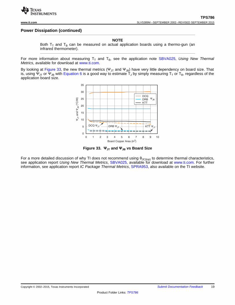
NOTEBoth TT and TB can be measured on actual application boards using a thermo-gun (aninfrared thermometer).
For more information about measuring TT and TB, see the application note SBVA025, Using New ThermalMetrics, available for download at www.ti.com.
By looking at Figure 33, the new thermal metrics (ΨJT and ΨJB) have very little dependency on board size. Thatis, using ΨJT or ΨJB with Equation 6 is a good way to estimate TJ by simply measuring TT or TB, regardless of theapplication board size.
Figure 33. ΨJT and ΨJB vs Board Size
For a more detailed discussion of why TI does not recommend using θJC(top) to determine thermal characteristics,see application report Using New Thermal Metrics, SBVA025, available for download at www.ti.com. For furtherinformation, see application report IC Package Thermal Metrics, SPRA953, also available on the TI website.
Copyright © 2002–2015, Texas Instruments Incorporated Submit Documentation Feedback 19
Product Folder Links: TPS786

(a) Example DRB (VSON) Package Measurement (b) Example DCQ (SOT-223) Package Measurement
1mm
T on topT
of IC
T on PCBB
surface
(c) Example KTT (TO-263) Package Measurement
1mm X
X
TT
TB
1mm
T on of ICT top(1)
T on PCBB
surface(2)
TPS786SLVS389M –SEPTEMBER 2002–REVISED SEPTEMBER 2015 www.ti.com
(1) TT is measured at the center of both the X- and Y-dimensional axes.(2) TB is measured below the package lead on the PCB surface.
Figure 34. Measuring Points for TT and TB
20 Submit Documentation Feedback Copyright © 2002–2015, Texas Instruments Incorporated
Product Folder Links: TPS786

TPS786www.ti.com SLVS389M –SEPTEMBER 2002–REVISED SEPTEMBER 2015
11 Device and Documentation Support
11.1 Device Support
11.1.1 Development Support
11.1.1.1 Evaluation ModulesAn evaluation module (EVM) is available to assist in the initial circuit performance evaluation using the TPS786.This EVM, TPS78601DRBEVM Single Output LDO, can be requested at the Texas Instruments website throughthe product folders or purchased directly from the TI eStore.
11.1.1.2 Spice ModelsComputer simulation of circuit performance using SPICE is often useful when analyzing the performance ofanalog circuits and systems. A SPICE model for the TPS786 devices are available through the product foldersunder simulation models.
11.1.2 Device Nomenclature
Table 2. Ordering InformationPRODUCT VOUT
(1)
TPS786xxyyyz XX is nominal output voltage (for example, 28 = 2.8 V, 285 = 2.85 V, 01 = Adjustable).YYY is package designator.Z is package quantity.
(1) Output voltages from 1.3 V to 5.0 V in 100-mV increments are available; minimum order quantities may apply. Contact factory for detailsand availability.
11.2 Documentation Support
11.2.1 Related DocumentationFor related documentation see the following:• Using New Thermal Metrics, SBVA025.• Semiconductor and IC Package Thermal Metrics, SPRA953.• Solder Pad Recommendations for Surface-Mount Devices, SBFA015.
11.3 Community ResourcesThe following links connect to TI community resources. Linked contents are provided "AS IS" by the respectivecontributors. They do not constitute TI specifications and do not necessarily reflect TI's views; see TI's Terms ofUse.
TI E2E™ Online Community TI's Engineer-to-Engineer (E2E) Community. Created to foster collaborationamong engineers. At e2e.ti.com, you can ask questions, share knowledge, explore ideas and helpsolve problems with fellow engineers.
Design Support TI's Design Support Quickly find helpful E2E forums along with design support tools andcontact information for technical support.
11.4 TrademarksE2E is a trademark of Texas Instruments.PowerPAD is a trademark of Texas Instruments Inc.Bluetooth is a registered trademark of Bluetooth SIG, Inc.All other trademarks are the property of their respective owners.
11.5 Electrostatic Discharge CautionThese devices have limited built-in ESD protection. The leads should be shorted together or the device placed in conductive foamduring storage or handling to prevent electrostatic damage to the MOS gates.
Copyright © 2002–2015, Texas Instruments Incorporated Submit Documentation Feedback 21
Product Folder Links: TPS786

TPS786SLVS389M –SEPTEMBER 2002–REVISED SEPTEMBER 2015 www.ti.com
11.6 GlossarySLYZ022 — TI Glossary.
This glossary lists and explains terms, acronyms, and definitions.
12 Mechanical, Packaging, and Orderable InformationThe following pages include mechanical, packaging, and orderable information. This information is the mostcurrent data available for the designated devices. This data is subject to change without notice and revision ofthis document. For browser-based versions of this data sheet, refer to the left-hand navigation.
22 Submit Documentation Feedback Copyright © 2002–2015, Texas Instruments Incorporated
Product Folder Links: TPS786

PACKAGE OPTION ADDENDUM
www.ti.com 17-Aug-2017
Addendum-Page 1
PACKAGING INFORMATION
Orderable Device Status(1)
Package Type PackageDrawing
Pins PackageQty
Eco Plan(2)
Lead/Ball Finish(6)
MSL Peak Temp(3)
Op Temp (°C) Device Marking(4/5)
Samples
TPS78601DCQ ACTIVE SOT-223 DCQ 6 78 Green (RoHS& no Sb/Br)
CU SN Level-2-260C-1 YEAR -40 to 125 PS78601
TPS78601DCQR ACTIVE SOT-223 DCQ 6 2500 Green (RoHS& no Sb/Br)
CU SN Level-2-260C-1 YEAR -40 to 125 PS78601
TPS78601DCQRG4 ACTIVE SOT-223 DCQ 6 2500 Green (RoHS& no Sb/Br)
CU NIPDAU Level-2-260C-1 YEAR -40 to 125 PS78601
TPS78601DRBR ACTIVE SON DRB 8 3000 Green (RoHS& no Sb/Br)
CU NIPDAU Level-2-260C-1 YEAR -40 to 125 OCI
TPS78601DRBT ACTIVE SON DRB 8 250 Green (RoHS& no Sb/Br)
CU NIPDAU Level-2-260C-1 YEAR -40 to 125 OCI
TPS78601KTTR ACTIVE DDPAK/TO-263
KTT 5 500 Green (RoHS& no Sb/Br)
CU SN Level-2-260C-1 YEAR TPS78601
TPS78601KTTRG3 ACTIVE DDPAK/TO-263
KTT 5 500 Green (RoHS& no Sb/Br)
CU SN Level-2-260C-1 YEAR TPS78601
TPS78601KTTT ACTIVE DDPAK/TO-263
KTT 5 50 Green (RoHS& no Sb/Br)
CU SN Level-2-260C-1 YEAR -40 to 125 TPS78601
TPS78601KTTTG3 ACTIVE DDPAK/TO-263
KTT 5 50 Green (RoHS& no Sb/Br)
CU SN Level-2-260C-1 YEAR -40 to 125 TPS78601
TPS78618DCQ ACTIVE SOT-223 DCQ 6 78 Green (RoHS& no Sb/Br)
CU NIPDAU Level-2-260C-1 YEAR -40 to 125 PS78618
TPS78618DCQR ACTIVE SOT-223 DCQ 6 2500 Green (RoHS& no Sb/Br)
CU NIPDAU Level-2-260C-1 YEAR -40 to 125 PS78618
TPS78618DCQRG4 ACTIVE SOT-223 DCQ 6 2500 Green (RoHS& no Sb/Br)
CU NIPDAU Level-2-260C-1 YEAR -40 to 125 PS78618
TPS78618KTTR ACTIVE DDPAK/TO-263
KTT 5 500 Green (RoHS& no Sb/Br)
CU SN Level-2-260C-1 YEAR TPS78618
TPS78618KTTRE3 ACTIVE DDPAK/TO-263
KTT 5 500 Green (RoHS& no Sb/Br)
CU SN Level-2-260C-1 YEAR TPS78618
TPS78618KTTRG3 ACTIVE DDPAK/TO-263
KTT 5 500 Green (RoHS& no Sb/Br)
CU SN Level-2-260C-1 YEAR TPS78618
TPS78618KTTT ACTIVE DDPAK/TO-263
KTT 5 50 Green (RoHS& no Sb/Br)
CU SN Level-2-260C-1 YEAR -40 to 125 TPS78618
TPS78618KTTTG3 ACTIVE DDPAK/TO-263
KTT 5 50 Green (RoHS& no Sb/Br)
CU SN Level-2-260C-1 YEAR -40 to 125 TPS78618

PACKAGE OPTION ADDENDUM
www.ti.com 17-Aug-2017
Addendum-Page 2
Orderable Device Status(1)
Package Type PackageDrawing
Pins PackageQty
Eco Plan(2)
Lead/Ball Finish(6)
MSL Peak Temp(3)
Op Temp (°C) Device Marking(4/5)
Samples
TPS78625DCQ ACTIVE SOT-223 DCQ 6 78 Green (RoHS& no Sb/Br)
CU NIPDAU Level-2-260C-1 YEAR -40 to 125 PS78625
TPS78625DCQG4 ACTIVE SOT-223 DCQ 6 78 Green (RoHS& no Sb/Br)
CU NIPDAU Level-2-260C-1 YEAR -40 to 125 PS78625
TPS78625DCQR ACTIVE SOT-223 DCQ 6 2500 Green (RoHS& no Sb/Br)
CU NIPDAU Level-2-260C-1 YEAR -40 to 125 PS78625
TPS78625DCQRG4 ACTIVE SOT-223 DCQ 6 2500 Green (RoHS& no Sb/Br)
CU NIPDAU Level-2-260C-1 YEAR -40 to 125 PS78625
TPS78625KTTR ACTIVE DDPAK/TO-263
KTT 5 500 Green (RoHS& no Sb/Br)
CU SN Level-2-260C-1 YEAR TPS78625
TPS78625KTTT ACTIVE DDPAK/TO-263
KTT 5 50 Green (RoHS& no Sb/Br)
CU SN Level-2-260C-1 YEAR -40 to 125 TPS78625
TPS78625KTTTG3 ACTIVE DDPAK/TO-263
KTT 5 50 Green (RoHS& no Sb/Br)
CU SN Level-2-260C-1 YEAR -40 to 125 TPS78625
TPS78628DCQR ACTIVE SOT-223 DCQ 6 2500 Green (RoHS& no Sb/Br)
CU NIPDAU Level-2-260C-1 YEAR -40 to 125 PS78628
TPS78628KTTT ACTIVE DDPAK/TO-263
KTT 5 50 Green (RoHS& no Sb/Br)
CU SN Level-2-260C-1 YEAR -40 to 125 TPS78628
TPS78630DCQ ACTIVE SOT-223 DCQ 6 78 Green (RoHS& no Sb/Br)
CU NIPDAU Level-2-260C-1 YEAR -40 to 125 PS78630
TPS78630DCQR ACTIVE SOT-223 DCQ 6 2500 Green (RoHS& no Sb/Br)
CU NIPDAU Level-2-260C-1 YEAR -40 to 125 PS78630
TPS78630KTTT ACTIVE DDPAK/TO-263
KTT 5 50 Green (RoHS& no Sb/Br)
CU SN Level-2-260C-1 YEAR -40 to 125 TPS78630
TPS78630KTTTG3 ACTIVE DDPAK/TO-263
KTT 5 50 Green (RoHS& no Sb/Br)
CU SN Level-2-260C-1 YEAR -40 to 125 TPS78630
TPS78633DCQ ACTIVE SOT-223 DCQ 6 78 Green (RoHS& no Sb/Br)
CU NIPDAU Level-2-260C-1 YEAR -40 to 125 PS78633
TPS78633DCQG4 ACTIVE SOT-223 DCQ 6 78 Green (RoHS& no Sb/Br)
CU NIPDAU Level-2-260C-1 YEAR -40 to 125 PS78633
TPS78633DCQR ACTIVE SOT-223 DCQ 6 2500 Green (RoHS& no Sb/Br)
CU NIPDAU Level-2-260C-1 YEAR -40 to 125 PS78633
TPS78633DCQRG4 ACTIVE SOT-223 DCQ 6 2500 Green (RoHS& no Sb/Br)
CU NIPDAU Level-2-260C-1 YEAR -40 to 125 PS78633
TPS78633KTTR ACTIVE DDPAK/TO-263
KTT 5 500 Green (RoHS& no Sb/Br)
CU SN Level-2-260C-1 YEAR TPS78633

PACKAGE OPTION ADDENDUM
www.ti.com 17-Aug-2017
Addendum-Page 3
Orderable Device Status(1)
Package Type PackageDrawing
Pins PackageQty
Eco Plan(2)
Lead/Ball Finish(6)
MSL Peak Temp(3)
Op Temp (°C) Device Marking(4/5)
Samples
TPS78633KTTRE3 ACTIVE DDPAK/TO-263
KTT 5 500 Green (RoHS& no Sb/Br)
CU SN Level-2-260C-1 YEAR TPS78633
TPS78633KTTRG3 ACTIVE DDPAK/TO-263
KTT 5 500 Green (RoHS& no Sb/Br)
CU SN Level-2-260C-1 YEAR TPS78633
TPS78633KTTT ACTIVE DDPAK/TO-263
KTT 5 50 Green (RoHS& no Sb/Br)
CU SN Level-2-260C-1 YEAR -40 to 125 TPS78633
TPS78633KTTTG3 ACTIVE DDPAK/TO-263
KTT 5 50 Green (RoHS& no Sb/Br)
CU SN Level-2-260C-1 YEAR -40 to 125 TPS78633
(1) The marketing status values are defined as follows:ACTIVE: Product device recommended for new designs.LIFEBUY: TI has announced that the device will be discontinued, and a lifetime-buy period is in effect.NRND: Not recommended for new designs. Device is in production to support existing customers, but TI does not recommend using this part in a new design.PREVIEW: Device has been announced but is not in production. Samples may or may not be available.OBSOLETE: TI has discontinued the production of the device.
(2) RoHS: TI defines "RoHS" to mean semiconductor products that are compliant with the current EU RoHS requirements for all 10 RoHS substances, including the requirement that RoHS substancedo not exceed 0.1% by weight in homogeneous materials. Where designed to be soldered at high temperatures, "RoHS" products are suitable for use in specified lead-free processes. TI mayreference these types of products as "Pb-Free".RoHS Exempt: TI defines "RoHS Exempt" to mean products that contain lead but are compliant with EU RoHS pursuant to a specific EU RoHS exemption.Green: TI defines "Green" to mean the content of Chlorine (Cl) and Bromine (Br) based flame retardants meet JS709B low halogen requirements of <=1000ppm threshold. Antimony trioxide basedflame retardants must also meet the <=1000ppm threshold requirement.
(3) MSL, Peak Temp. - The Moisture Sensitivity Level rating according to the JEDEC industry standard classifications, and peak solder temperature.
(4) There may be additional marking, which relates to the logo, the lot trace code information, or the environmental category on the device.
(5) Multiple Device Markings will be inside parentheses. Only one Device Marking contained in parentheses and separated by a "~" will appear on a device. If a line is indented then it is a continuationof the previous line and the two combined represent the entire Device Marking for that device.
(6) Lead/Ball Finish - Orderable Devices may have multiple material finish options. Finish options are separated by a vertical ruled line. Lead/Ball Finish values may wrap to two lines if the finishvalue exceeds the maximum column width.
Important Information and Disclaimer:The information provided on this page represents TI's knowledge and belief as of the date that it is provided. TI bases its knowledge and belief on informationprovided by third parties, and makes no representation or warranty as to the accuracy of such information. Efforts are underway to better integrate information from third parties. TI has taken andcontinues to take reasonable steps to provide representative and accurate information but may not have conducted destructive testing or chemical analysis on incoming materials and chemicals.TI and TI suppliers consider certain information to be proprietary, and thus CAS numbers and other limited information may not be available for release.

PACKAGE OPTION ADDENDUM
www.ti.com 17-Aug-2017
Addendum-Page 4
In no event shall TI's liability arising out of such information exceed the total purchase price of the TI part(s) at issue in this document sold by TI to Customer on an annual basis.

TAPE AND REEL INFORMATION
*All dimensions are nominal
Device PackageType
PackageDrawing
Pins SPQ ReelDiameter
(mm)
ReelWidth
W1 (mm)
A0(mm)
B0(mm)
K0(mm)
P1(mm)
W(mm)
Pin1Quadrant
TPS78601DCQR SOT-223 DCQ 6 2500 330.0 12.4 7.1 7.45 1.88 8.0 12.0 Q3
TPS78601DCQRG4 SOT-223 DCQ 6 2500 330.0 12.4 7.1 7.45 1.88 8.0 12.0 Q3
TPS78601DRBR SON DRB 8 3000 330.0 12.4 3.3 3.3 1.1 8.0 12.0 Q2
TPS78601DRBT SON DRB 8 250 180.0 12.4 3.3 3.3 1.1 8.0 12.0 Q2
TPS78601KTTR DDPAK/TO-263
KTT 5 500 330.0 24.4 10.6 15.6 4.9 16.0 24.0 Q2
TPS78601KTTT DDPAK/TO-263
KTT 5 50 330.0 24.4 10.6 15.6 4.9 16.0 24.0 Q2
TPS78618DCQR SOT-223 DCQ 6 2500 330.0 12.4 7.1 7.45 1.88 8.0 12.0 Q3
TPS78618KTTR DDPAK/TO-263
KTT 5 500 330.0 24.4 10.6 15.6 4.9 16.0 24.0 Q2
TPS78618KTTRE3 DDPAK/TO-263
KTT 5 500 330.0 24.4 10.6 15.6 4.9 16.0 24.0 Q2
TPS78618KTTT DDPAK/TO-263
KTT 5 50 330.0 24.4 10.6 15.6 4.9 16.0 24.0 Q2
TPS78625DCQR SOT-223 DCQ 6 2500 330.0 12.4 7.1 7.45 1.88 8.0 12.0 Q3
TPS78625KTTR DDPAK/TO-263
KTT 5 500 330.0 24.4 10.6 15.6 4.9 16.0 24.0 Q2
TPS78625KTTT DDPAK/TO-263
KTT 5 50 330.0 24.4 10.6 15.6 4.9 16.0 24.0 Q2
PACKAGE MATERIALS INFORMATION
www.ti.com 17-Aug-2017
Pack Materials-Page 1
Device PackageType
PackageDrawing
Pins SPQ ReelDiameter
(mm)
ReelWidth
W1 (mm)
A0(mm)
B0(mm)
K0(mm)
P1(mm)
W(mm)
Pin1Quadrant
TPS78628DCQR SOT-223 DCQ 6 2500 330.0 12.4 7.1 7.45 1.88 8.0 12.0 Q3
TPS78628KTTT DDPAK/TO-263
KTT 5 50 330.0 24.4 10.6 15.6 4.9 16.0 24.0 Q2
TPS78630DCQR SOT-223 DCQ 6 2500 330.0 12.4 7.1 7.45 1.88 8.0 12.0 Q3
TPS78630KTTT DDPAK/TO-263
KTT 5 50 330.0 24.4 10.6 15.6 4.9 16.0 24.0 Q2
TPS78633DCQR SOT-223 DCQ 6 2500 330.0 12.4 7.1 7.45 1.88 8.0 12.0 Q3
TPS78633KTTR DDPAK/TO-263
KTT 5 500 330.0 24.4 10.6 15.6 4.9 16.0 24.0 Q2
TPS78633KTTRE3 DDPAK/TO-263
KTT 5 500 330.0 24.4 10.6 15.6 4.9 16.0 24.0 Q2
TPS78633KTTT DDPAK/TO-263
KTT 5 50 330.0 24.4 10.6 15.6 4.9 16.0 24.0 Q2
*All dimensions are nominal
Device Package Type Package Drawing Pins SPQ Length (mm) Width (mm) Height (mm)
TPS78601DCQR SOT-223 DCQ 6 2500 367.0 367.0 35.0
TPS78601DCQRG4 SOT-223 DCQ 6 2500 346.0 346.0 29.0
TPS78601DRBR SON DRB 8 3000 367.0 367.0 35.0
TPS78601DRBT SON DRB 8 250 210.0 185.0 35.0
TPS78601KTTR DDPAK/TO-263 KTT 5 500 367.0 367.0 45.0
PACKAGE MATERIALS INFORMATION
www.ti.com 17-Aug-2017
Pack Materials-Page 2
Device Package Type Package Drawing Pins SPQ Length (mm) Width (mm) Height (mm)
TPS78601KTTT DDPAK/TO-263 KTT 5 50 367.0 367.0 45.0
TPS78618DCQR SOT-223 DCQ 6 2500 346.0 346.0 29.0
TPS78618KTTR DDPAK/TO-263 KTT 5 500 367.0 367.0 45.0
TPS78618KTTRE3 DDPAK/TO-263 KTT 5 500 367.0 367.0 45.0
TPS78618KTTT DDPAK/TO-263 KTT 5 50 367.0 367.0 45.0
TPS78625DCQR SOT-223 DCQ 6 2500 346.0 346.0 29.0
TPS78625KTTR DDPAK/TO-263 KTT 5 500 367.0 367.0 45.0
TPS78625KTTT DDPAK/TO-263 KTT 5 50 367.0 367.0 45.0
TPS78628DCQR SOT-223 DCQ 6 2500 346.0 346.0 41.0
TPS78628KTTT DDPAK/TO-263 KTT 5 50 367.0 367.0 45.0
TPS78630DCQR SOT-223 DCQ 6 2500 346.0 346.0 41.0
TPS78630KTTT DDPAK/TO-263 KTT 5 50 367.0 367.0 45.0
TPS78633DCQR SOT-223 DCQ 6 2500 346.0 346.0 29.0
TPS78633KTTR DDPAK/TO-263 KTT 5 500 367.0 367.0 45.0
TPS78633KTTRE3 DDPAK/TO-263 KTT 5 500 367.0 367.0 45.0
TPS78633KTTT DDPAK/TO-263 KTT 5 50 367.0 367.0 45.0
PACKAGE MATERIALS INFORMATION
www.ti.com 17-Aug-2017
Pack Materials-Page 3


www.ti.com
PACKAGE OUTLINE
C
8X 0.350.25
2.4 0.052X
1.95
1.65 0.05
6X 0.65
1 MAX
8X 0.50.3
0.050.00
A 3.12.9
B
3.12.9
(0.2) TYP
VSON - 1 mm max heightDRB0008BPLASTIC SMALL OUTLINE - NO LEAD
4218876/A 12/2017
PIN 1 INDEX AREA
SEATING PLANE
0.08 C
1
4 5
8
(OPTIONAL)PIN 1 ID 0.1 C A B
0.05 C
THERMAL PADEXPOSED
NOTES: 1. All linear dimensions are in millimeters. Any dimensions in parenthesis are for reference only. Dimensioning and tolerancing per ASME Y14.5M. 2. This drawing is subject to change without notice. 3. The package thermal pad must be soldered to the printed circuit board for thermal and mechanical performance.
SCALE 4.000

www.ti.com
EXAMPLE BOARD LAYOUT
0.07 MINALL AROUND
0.07 MAXALL AROUND
8X (0.3)
(2.4)
(2.8)
6X (0.65)
(1.65)
( 0.2) VIATYP
(0.575)
(0.95)
8X (0.6)
(R0.05) TYP
VSON - 1 mm max heightDRB0008BPLASTIC SMALL OUTLINE - NO LEAD
4218876/A 12/2017
SYMM
1
45
8
LAND PATTERN EXAMPLESCALE:20X
NOTES: (continued) 4. This package is designed to be soldered to a thermal pad on the board. For more information, see Texas Instruments literature number SLUA271 (www.ti.com/lit/slua271).5. Vias are optional depending on application, refer to device data sheet. If any vias are implemented, refer to their locations shown on this view. It is recommended that vias under paste be filled, plugged or tented.
SOLDER MASKOPENINGSOLDER MASK
METAL UNDER
SOLDER MASKDEFINED
METALSOLDER MASKOPENING
SOLDER MASK DETAILS
NON SOLDER MASKDEFINED
(PREFERRED)

www.ti.com
EXAMPLE STENCIL DESIGN
(R0.05) TYP
8X (0.3)
8X (0.6)
(1.47)
(1.06)
(2.8)
(0.63)
6X (0.65)
VSON - 1 mm max heightDRB0008BPLASTIC SMALL OUTLINE - NO LEAD
4218876/A 12/2017
NOTES: (continued) 6. Laser cutting apertures with trapezoidal walls and rounded corners may offer better paste release. IPC-7525 may have alternate design recommendations.
SOLDER PASTE EXAMPLEBASED ON 0.125 mm THICK STENCIL
EXPOSED PAD
81% PRINTED SOLDER COVERAGE BY AREASCALE:25X
SYMM
1
4 5
8
METALTYP
SYMM


IMPORTANT NOTICE
Texas Instruments Incorporated (TI) reserves the right to make corrections, enhancements, improvements and other changes to itssemiconductor products and services per JESD46, latest issue, and to discontinue any product or service per JESD48, latest issue. Buyersshould obtain the latest relevant information before placing orders and should verify that such information is current and complete.TI’s published terms of sale for semiconductor products (http://www.ti.com/sc/docs/stdterms.htm) apply to the sale of packaged integratedcircuit products that TI has qualified and released to market. Additional terms may apply to the use or sale of other types of TI products andservices.Reproduction of significant portions of TI information in TI data sheets is permissible only if reproduction is without alteration and isaccompanied by all associated warranties, conditions, limitations, and notices. TI is not responsible or liable for such reproduceddocumentation. Information of third parties may be subject to additional restrictions. Resale of TI products or services with statementsdifferent from or beyond the parameters stated by TI for that product or service voids all express and any implied warranties for theassociated TI product or service and is an unfair and deceptive business practice. TI is not responsible or liable for any such statements.Buyers and others who are developing systems that incorporate TI products (collectively, “Designers”) understand and agree that Designersremain responsible for using their independent analysis, evaluation and judgment in designing their applications and that Designers havefull and exclusive responsibility to assure the safety of Designers' applications and compliance of their applications (and of all TI productsused in or for Designers’ applications) with all applicable regulations, laws and other applicable requirements. Designer represents that, withrespect to their applications, Designer has all the necessary expertise to create and implement safeguards that (1) anticipate dangerousconsequences of failures, (2) monitor failures and their consequences, and (3) lessen the likelihood of failures that might cause harm andtake appropriate actions. Designer agrees that prior to using or distributing any applications that include TI products, Designer willthoroughly test such applications and the functionality of such TI products as used in such applications.TI’s provision of technical, application or other design advice, quality characterization, reliability data or other services or information,including, but not limited to, reference designs and materials relating to evaluation modules, (collectively, “TI Resources”) are intended toassist designers who are developing applications that incorporate TI products; by downloading, accessing or using TI Resources in anyway, Designer (individually or, if Designer is acting on behalf of a company, Designer’s company) agrees to use any particular TI Resourcesolely for this purpose and subject to the terms of this Notice.TI’s provision of TI Resources does not expand or otherwise alter TI’s applicable published warranties or warranty disclaimers for TIproducts, and no additional obligations or liabilities arise from TI providing such TI Resources. TI reserves the right to make corrections,enhancements, improvements and other changes to its TI Resources. TI has not conducted any testing other than that specificallydescribed in the published documentation for a particular TI Resource.Designer is authorized to use, copy and modify any individual TI Resource only in connection with the development of applications thatinclude the TI product(s) identified in such TI Resource. NO OTHER LICENSE, EXPRESS OR IMPLIED, BY ESTOPPEL OR OTHERWISETO ANY OTHER TI INTELLECTUAL PROPERTY RIGHT, AND NO LICENSE TO ANY TECHNOLOGY OR INTELLECTUAL PROPERTYRIGHT OF TI OR ANY THIRD PARTY IS GRANTED HEREIN, including but not limited to any patent right, copyright, mask work right, orother intellectual property right relating to any combination, machine, or process in which TI products or services are used. Informationregarding or referencing third-party products or services does not constitute a license to use such products or services, or a warranty orendorsement thereof. Use of TI Resources may require a license from a third party under the patents or other intellectual property of thethird party, or a license from TI under the patents or other intellectual property of TI.TI RESOURCES ARE PROVIDED “AS IS” AND WITH ALL FAULTS. TI DISCLAIMS ALL OTHER WARRANTIES ORREPRESENTATIONS, EXPRESS OR IMPLIED, REGARDING RESOURCES OR USE THEREOF, INCLUDING BUT NOT LIMITED TOACCURACY OR COMPLETENESS, TITLE, ANY EPIDEMIC FAILURE WARRANTY AND ANY IMPLIED WARRANTIES OFMERCHANTABILITY, FITNESS FOR A PARTICULAR PURPOSE, AND NON-INFRINGEMENT OF ANY THIRD PARTY INTELLECTUALPROPERTY RIGHTS. TI SHALL NOT BE LIABLE FOR AND SHALL NOT DEFEND OR INDEMNIFY DESIGNER AGAINST ANY CLAIM,INCLUDING BUT NOT LIMITED TO ANY INFRINGEMENT CLAIM THAT RELATES TO OR IS BASED ON ANY COMBINATION OFPRODUCTS EVEN IF DESCRIBED IN TI RESOURCES OR OTHERWISE. IN NO EVENT SHALL TI BE LIABLE FOR ANY ACTUAL,DIRECT, SPECIAL, COLLATERAL, INDIRECT, PUNITIVE, INCIDENTAL, CONSEQUENTIAL OR EXEMPLARY DAMAGES INCONNECTION WITH OR ARISING OUT OF TI RESOURCES OR USE THEREOF, AND REGARDLESS OF WHETHER TI HAS BEENADVISED OF THE POSSIBILITY OF SUCH DAMAGES.Unless TI has explicitly designated an individual product as meeting the requirements of a particular industry standard (e.g., ISO/TS 16949and ISO 26262), TI is not responsible for any failure to meet such industry standard requirements.Where TI specifically promotes products as facilitating functional safety or as compliant with industry functional safety standards, suchproducts are intended to help enable customers to design and create their own applications that meet applicable functional safety standardsand requirements. Using products in an application does not by itself establish any safety features in the application. Designers mustensure compliance with safety-related requirements and standards applicable to their applications. Designer may not use any TI products inlife-critical medical equipment unless authorized officers of the parties have executed a special contract specifically governing such use.Life-critical medical equipment is medical equipment where failure of such equipment would cause serious bodily injury or death (e.g., lifesupport, pacemakers, defibrillators, heart pumps, neurostimulators, and implantables). Such equipment includes, without limitation, allmedical devices identified by the U.S. Food and Drug Administration as Class III devices and equivalent classifications outside the U.S.TI may expressly designate certain products as completing a particular qualification (e.g., Q100, Military Grade, or Enhanced Product).Designers agree that it has the necessary expertise to select the product with the appropriate qualification designation for their applicationsand that proper product selection is at Designers’ own risk. Designers are solely responsible for compliance with all legal and regulatoryrequirements in connection with such selection.Designer will fully indemnify TI and its representatives against any damages, costs, losses, and/or liabilities arising out of Designer’s non-compliance with the terms and provisions of this Notice.
Mailing Address: Texas Instruments, Post Office Box 655303, Dallas, Texas 75265Copyright © 2018, Texas Instruments Incorporated