Embed Size (px)
Citation preview

VSENSE
GND
PH5.3 V
BOOT
VIN
RT/CLK
SS
Supply
nRST
DELAY
VREGIGN_EN
5 V
3.3 VSENSE
3.3 VDRIVE
3.3 VBOOT_LDO
COMP
1.2 VSENSE
1.2 VDRIVE
1.234 V
5 V
VIN_D
EN
S1
L
S2
T1
T2
3 k
C3
10 µF
C1
C2
2.2 µF
0.1
µF
R1
R12
CO
2
4
9
5
8
20
6
12
21
16
17
23
10
18
19
22
14
15
1
3
24PGND
CI
1µF 2.2 µF
10 µF
2.2 µF
5.3 W
10
µF
240
660
TPS65300-Q1
VI = 5.6 V to 40 V
Product
Folder
Sample &Buy
Technical
Documents
Tools &
Software
Support &Community
TPS65300-Q1SLVSBB6F –MARCH 2012–REVISED JULY 2015
TPS65300-Q1 3-MHz Step-Down Regulator and Triple Linear Regulators1 Features 3 Description
The TPS65300-Q1 power supply is a combination of1• Qualified for Automotive Applications
a single switch-mode buck power supply and three• AEC-Q100 Qualified with the Following Results linear regulators. This device is a monolithic high-– Device Temperature Grade 1: –40°C to 125°C voltage switching regulator with an integrated 1.2-A
Ambient Operating Temperature Range peak current switch, 45-V power MOSFET, and onelow-voltage linear regulator and two voltage-regulator– Device HBM ESD Classification Level H2controllers.– Device CDM ESD Classification Level C4BThe device has a voltage supervisor which monitors• Input VIN Range 5.6 V to 40 V, With Transientsthe output of the switch-mode power supply, theup to 45 V3.3-V linear regulator, and the 1.234-V linear
• All Outputs Support Ceramic Output Capacitors regulator. An external timing capacitor is used to setfor Stability the power-on delay and the release of the reset
• Switch-Mode Regulator With Integrated High-Side output nRST. This reset output is also used toindicate if the switch-mode supply, the 3.3-V linearSwitchregulator supply, or the 1.234-V linear regulator– Recommended Switch-Mode Frequency supply is outside the set limits. The 5-V regulatorRange 2 MHz to 3 MHz tracks the 3.3-V linear regulator within the specified
– Overcurrent Protection and 1.2-A Peak Switch limits.Current
The TPS65300-Q1 device has a switching frequency• One Linear Regulators and Two Linear Regulator range from 2 MHz to 3 MHz, allowing the use of low-
Controllers With 0.8-V ±1.5% Reference profile inductors and low-value input and outputceramic capacitors. External loop compensation gives• Status Indicator Output of IGN_EN Inputthe user the flexibility to optimize the converter• Soft Start on Ignition (IGN_EN)/Enable Input (EN)response for the appropriate operating conditions.CycleThis device has built-in protection features such as• External Clock Input for Synchronizationsoft start on IGN_EN ON or enables cycle, pulse-by-• Programmable Power-On-Reset Delay, Reset- pulse current-limit, thermal sensing, and shutdownFunction Filter Timer for Fast Negative Transients because of excessive power dissipation.
• Voltage Supervisor for the Following SuppliesDevice Information– VREG, 3.3 V, 1.234 V
PART NUMBER PACKAGE BODY SIZE (NOM)• Thermal Shutdown Protection for ExcessiveHTSSOP (24) 7.80 mm × 4.40 mmPower Dissipation TPS65300-Q1VQFN (24) 5.00 mm × 4.00 mm• Operating Junction Temperature Range: –40°C to
150°CTypical Application Schematic• Thermally Enhanced 24-Pin HTSSOP or 24-Pin
VQFN Package
2 Applications• Power Supply for TMS570 Microcontrollers• Power Supply for C28XXX DSP• General-Purpose Power Supply for Automotive
Applications– Microcontroller and DSP
1
An IMPORTANT NOTICE at the end of this data sheet addresses availability, warranty, changes, use in safety-critical applications,intellectual property matters and other important disclaimers. PRODUCTION DATA.

TPS65300-Q1SLVSBB6F –MARCH 2012–REVISED JULY 2015 www.ti.com
Table of Contents7.2 Functional Block Diagram ....................................... 101 Features .................................................................. 17.3 Feature Description................................................. 112 Applications ........................................................... 17.4 Device Functional Modes........................................ 153 Description ............................................................. 1
8 Application and Implementation ........................ 174 Revision History..................................................... 28.1 Application Information............................................ 175 Pin Configuration and Functions ......................... 38.2 Typical Application .................................................. 176 Specifications......................................................... 4
9 Power Supply Recommendations ...................... 266.1 Absolute Maximum Ratings ...................................... 410 Layout................................................................... 266.2 ESD Ratings.............................................................. 4
10.1 Layout Guidelines ................................................. 266.3 Recommended Operating Conditions....................... 410.2 Layout Example .................................................... 276.4 Thermal Information .................................................. 5
11 Device and Documentation Support ................. 286.5 DC Characteristics .................................................... 511.1 Device Support...................................................... 286.6 Timing Requirements ................................................ 711.2 Documentation Support ........................................ 286.7 Switching Characteristics .......................................... 711.3 Community Resource............................................ 286.8 Typical Characteristics .............................................. 811.4 Trademarks ........................................................... 286.9 5-V Linear Regulator (5VO) ....................................... 811.5 Electrostatic Discharge Caution............................ 286.10 3.3-V Linear Regulator Controller (3.3VO) .............. 911.6 Glossary ................................................................ 286.11 1.234-V Linear Regulator Controller (1.2VO) .......... 9
12 Mechanical, Packaging, and Orderable7 Detailed Description ............................................ 10Information ........................................................... 287.1 Overview ................................................................. 10
4 Revision HistoryNOTE: Page numbers for previous revisions may differ from page numbers in the current version.
Changes from Revision E (March 2014) to Revision F Page
• Changed the word terminal back to pin throughout the document ....................................................................................... 3• Changed the MIN, TYP, and MAX values for the 1.2VSENSE output voltage in the Electrical Characteristics table .......... 6• Changed the y-axis intervals for the 1.2VSENSE vs Temperature graph.............................................................................. 9
Changes from Revision D (August 2013) to Revision E Page
• Added the Device Information table and the following new sections: Power Supply Recommendations, Device andDocumentation Support, and Mechanical, Packaging, and Orderable Information................................................................ 1
• Changed the word pin to terminal throughout the document ................................................................................................ 3• Moved the Pin Functions section into the Pin Configuration and Functions section.............................................................. 3• Changed DC CHARACTERISTICS condition statement from TJ = –40°C to 150°C to TJ-Max = 150°C ................................. 5• Changed min value for VIL of IGN_EN from 2 to 2.2 in the DC CHARACTERISTICS table.................................................. 5• Moved all timing requirements out of the Electrical Characteristics table and into the Timing Requirements table ............. 7• Combined the general application equations with the practical equations to streamline the Typical Application
section ................................................................................................................................................................................. 18• Changed Y-axis name from Current (mA) to Efficiency in Figure 17 ................................................................................... 25• Moved the Efficiency vs Output Current on VREG graph and the scope plots from the Typical Characteristics
section to the Application Curves section ............................................................................................................................ 25
Changes from Revision C (April 2013) to Revision D Page
• Changed VIH max limit from 4 to 3.6 V in DC Characteristics table ....................................................................................... 5• Added 3.7 V condition and values to Input High IIH parameter in DC Characteristics table .................................................. 5• Changed ICharge unit from V to µA in DC Characteristics table ............................................................................................... 6• Changed internal resistor limit text in Ignition Enable Input, IGN_EN pin description ......................................................... 11
2 Submit Documentation Feedback Copyright © 2012–2015, Texas Instruments Incorporated
Product Folder Links: TPS65300-Q1

1
2
3
4
5
6
7
19
18
17
16
15
14
13
8 9 10 11 12
24 23 22 21 20
BOOT
VIN
IGN_EN
BOOT_LDO
5V
IGN
_S
T
GN
D
NC
CO
MP
NC
RT/CLK
EN
DELAY
SS
3.3VDRIVE
3.3VSENSE
1,2VDRIVE
1.2VSENSE
VSENSE
VIN
_D
PH
PG
ND
nR
ST
VR
EG
P0057-02
1
2
3
4
5
6
7
8
9
11
10
12
24
23
22
21
20
19
18
17
16
14
15
13
P0110-03
PH
VIN_D
BOOT
IGN_ST
VIN
IGN_EN
BOOT_LDO
NC
RT/CLK
EN
5V
GND
PGND
nRST
VREG
DELAY
SS
3.3VDRIVE
3.3VSENSE
1.2VDRIVE
1.2VSENSE
VSENSE
COMP
NC
TPS65300-Q1www.ti.com SLVSBB6F –MARCH 2012–REVISED JULY 2015
5 Pin Configuration and Functions
RHF Package PWP Package24-Pin VQFN With Exposed Thermal Pad 24-Pin HTSSOP With PowerPAD™
Top View Top View
Pin FunctionsPIN
NO. I/O DESCRIPTIONNAME
PWP RHF
1.2VDRIVE 17 15 O Output current source to drive the base of an external bipolar transistor to regulate the 1.234-V supply
1.2VSENSE 16 14 I Voltage node of 1.234-V supply
3.3VDRIVE 19 17 O Output current source to drive the base of an external bipolar transistor to regulate the 3.3-V supply
3.3VSENSE 18 16 I Voltage node of 3.3-V supply
5V 10 8 O External capacitor to ground for stability of regulated output
BOOT 3 1 O External bootstrap capacitor connected to PH (pin 1) to drive gate of internal switching FET
BOOT_LDO 6 4 O External capacitor connected to ground for stability of internal regulator
COMP 14 12 O Error amplifier output to connect external compensation components
DELAY 21 19 O External capacitor to ground to program the power-on-reset delay
EN 9 7 I A high logic-level input signal to enable and low signal to disable device. Internally pulled down to ground
GND 12 10 O Ground pin, must be electrically connected to exposed pad on PCB for proper thermal performance
IGN_EN 5 3 I Ignition input (high-voltage tolerant) internally pulls to ground. Must be externally pulled up to enable
Active-low, open-drain ignition input indicator, output connected to external bias voltage through a resistor. Asserted highIGN_ST 11 9 O after ignition input is high
7 5NC — Connect to ground
13 11
Active-low, open-drain reset output connected to external bias voltage through a resistor. This output is asserted highnRST 23 21 O after the preregulator, 3.3-V, and 1.234-V regulator outputs are regulating and the delay timer has expired. Also, output
is asserted low if any one of these three supplies is out of the set regulation, this threshold is internally set.
PGND 24 22 O Power ground pin, must be electrically connected to exposed pad on PCB for proper thermal performance
PH 1 23 O Source of internal switching FET
External resistor connected ground to program the internal oscillator. Alternative option is to feed an external clock toRT/CLK 8 6 I/O provide reference for switching frequency.
SS 20 18 O External capacitor to ground to program soft-start time
VIN 4 2 I Unregulated input voltage supply. Pins 2 and 4 must be connected together externally.
VIN_D 2 24 I Drain input for internal high-side MOSFET. Pins 2 and 4 must be connected together externally.
VREG 22 20 I Buck converter output. Integrated internal low-side FET to load output during startup or limit voltage overshoot
VSENSE 15 13 I Inverting node of error amplifier for voltage-mode control of preregulated supply
Thermal pad — Electrically connect to ground and solder to ground plane of PCB for thermal efficiency
Copyright © 2012–2015, Texas Instruments Incorporated Submit Documentation Feedback 3
Product Folder Links: TPS65300-Q1

TPS65300-Q1SLVSBB6F –MARCH 2012–REVISED JULY 2015 www.ti.com
6 Specifications
6.1 Absolute Maximum Ratingsover operating free-air temperature range (unless otherwise noted) (1)
MIN MAX UNITVIN, VIN_D –0.3 45 VBOOT –0.3 50 V
Buck regulator –1PH 45 V–2 for 30 nsVSENSE –0.3 5.5 VIGN_EN –0.3 45 V
ControlEN, 3.3VSENSE, 1.2VSENSE, RT/CLK, VREG –0.3 5.5 V3.3VDRIVE, 1.2VDRIVE –0.3 8 VnRST, IGN_ST –0.3 5.5 V
OutputDELAY, COMP –0.3 7 VBOOT_LDO, 5V –0.3 9 V
Operating junction temperature, TJ –40 150 °CStorage temperature, TstgMoved the storage temperature and ESD ratings out of the Absolute –55 165 °CMaximum Ratings table and into the new Handling Ratings table
(1) Stresses beyond those listed under Absolute Maximum Ratings may cause permanent damage to the device. These are stress ratingsonly, and functional operation of the device at these or any other conditions beyond those indicated under Recommended OperatingConditions is not implied. Exposure to absolute-maximum-rated conditions for extended periods may affect device reliability.
6.2 ESD RatingsVALUE UNIT
Human-body model (HBM), per AEC Q100-002 (1) ±2000All pins ±500V(ESD) Electrostatic discharge VCharged-device model (CDM), per AECCorner pins (1, 12, 13,Q100-011 ±750and 24)
(1) AEC Q100-002 indicates that HBM stressing shall be in accordance with the ANSI/ESDA/JEDEC JS-001 specification.
6.3 Recommended Operating Conditionsover operating free-air temperature range (unless otherwise noted)
MIN NOM MAX UNITVIN, VIN_D 5.6 40 VBOOT 5.6 48 VPH –1 40 VIGN_EN 0 40 VEN, VSENSE, 3.3VSENSE, 1.2VSENSE, RT/CLK, nRST, IGN_ST 0 5.25 VVREG, 3.3VDRIVE, 1.2VDRIVE 0 7.5 VSS, DELAY, COMP 0 6.5 VBOOT_LDO 0 8.1 VOperating ambient temperature range, TA –40 125 °C
4 Submit Documentation Feedback Copyright © 2012–2015, Texas Instruments Incorporated
Product Folder Links: TPS65300-Q1
TPS65300-Q1www.ti.com SLVSBB6F –MARCH 2012–REVISED JULY 2015
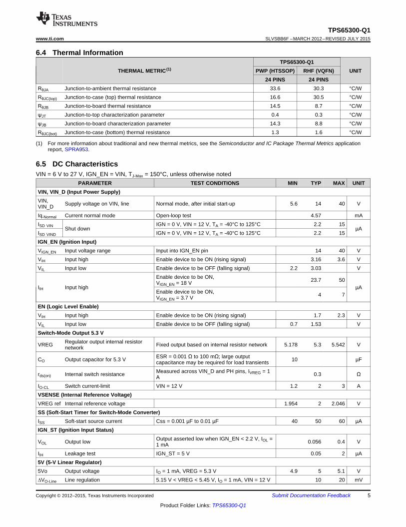
6.4 Thermal InformationTPS65300-Q1
THERMAL METRIC (1) PWP (HTSSOP) RHF (VQFN) UNIT24 PINS 24 PINS
RθJA Junction-to-ambient thermal resistance 33.6 30.3 °C/WRθJC(top) Junction-to-case (top) thermal resistance 16.6 30.5 °C/WRθJB Junction-to-board thermal resistance 14.5 8.7 °C/WψJT Junction-to-top characterization parameter 0.4 0.3 °C/WψJB Junction-to-board characterization parameter 14.3 8.8 °C/WRθJC(bot) Junction-to-case (bottom) thermal resistance 1.3 1.6 °C/W
(1) For more information about traditional and new thermal metrics, see the Semiconductor and IC Package Thermal Metrics applicationreport, SPRA953.
6.5 DC CharacteristicsVIN = 6 V to 27 V, IGN_EN = VIN, TJ-Max = 150°C, unless otherwise noted
PARAMETER TEST CONDITIONS MIN TYP MAX UNITVIN, VIN_D (Input Power Supply)VIN, Supply voltage on VIN, line Normal mode, after initial start-up 5.6 14 40 VVIN_DIq-Normal Current normal mode Open-loop test 4.57 mAISD VIN IGN = 0 V, VIN = 12 V, TA = -40°C to 125°C 2.2 15
Shut down µAISD VIND IGN = 0 V, VIN = 12 V, TA = -40°C to 125°C 2.2 15IGN_EN (Ignition Input)VIGN_EN Input voltage range Input into IGN_EN pin 14 40 VVIH Input high Enable device to be ON (rising signal) 3.16 3.6 VVIL Input low Enable device to be OFF (falling signal) 2.2 3.03 V
Enable device to be ON, 23.7 50VIGN_EN = 18 VIIH Input high µA
Enable device to be ON, 4 7VIGN_EN = 3.7 VEN (Logic Level Enable)VIH Input high Enable device to be ON (rising signal) 1.7 2.3 VVIL Input low Enable device to be OFF (falling signal) 0.7 1.53 VSwitch-Mode Output 5.3 V
Regulator output internal resistorVREG Fixed output based on internal resistor network 5.178 5.3 5.542 VnetworkESR = 0.001 Ω to 100 mΩ; large outputCO Output capacitor for 5.3 V 10 µFcapacitance may be required for load transientsMeasured across VIN_D and PH pins, IVREG = 1rds(on) Internal switch resistance 0.3 ΩA
IO-CL Switch current-limit VIN = 12 V 1.2 2 3 AVSENSE (Internal Reference Voltage)VREG ref Internal reference voltage 1.954 2 2.046 VSS (Soft-Start Timer for Switch-Mode Converter)ISS Soft-start source current Css = 0.001 µF to 0.01 µF 40 50 60 µAIGN_ST (Ignition Input Status)
Output asserted low when IGN_EN < 2.2 V, IOL =VOL Output low 0.056 0.4 V1 mAIIH Leakage test IGN_ST = 5 V 0.05 2 µA5V (5-V Linear Regulator)5Vo Output voltage IO = 1 mA, VREG = 5.3 V 4.9 5 5.1 V∆VO-Line Line regulation 5.15 V < VREG < 5.45 V, IO = 1 mA, VIN = 12 V 10 20 mV
Copyright © 2012–2015, Texas Instruments Incorporated Submit Documentation Feedback 5
Product Folder Links: TPS65300-Q1

TPS65300-Q1SLVSBB6F –MARCH 2012–REVISED JULY 2015 www.ti.com
DC Characteristics (continued)VIN = 6 V to 27 V, IGN_EN = VIN, TJ-Max = 150°C, unless otherwise noted
PARAMETER TEST CONDITIONS MIN TYP MAX UNIT∆VO-Load Load regulation 1 mA < IO < 200 mA, VREG = 5.3 V, VIN = 12 V 10 30 mV
IO = 150 mA, measure VREG when VO(nom) –VDO Dropout voltage 0.1 V, then VDO = VREG – (5VO – 0.1) V, VREG 0.15 0.26 V
> 5 VI5V-CL Current-limit 5VO = 0.8 × 5VO (nominal) 350 1080 mA
ESR = 0.001 Ω to 2 Ω. Larger output capacitanceCO Output capacitor 1 2.2 10 µFmay be required for load transients.f = 100 Hz, VREG = 5.3 V, IO = 100 mA, VIN =PSRR Power-supply rejection ratio 45 60 75 dB12 V
3.3-V Linear Regulator Controller (3.3VSENSE)3.3VO Output voltage Io = 5 mA, Vnpn_power input = 5.3 V 3.234 3.3 3.366 V∆3.3VO- 3.8 V < Vnpn_power input < 7 V (with nRST notLine regulation 1 10 mVLine triggered)∆3.3VO- Load regulation 5 mA < IO < 550 mA 7.5 30 mVLoad
ESR = 0.001 Ω to 2 Ω. Large output capacitanceCO Output capacitor for 3.3 V 1 4.7 10 µFmay be required for load transients.f = 100 Hz, VREG = 5.3 V, IO = 200 mA, VIN =PSRR Power-supply rejection ratio 45 60 75 dB12 V
3.3VDRIVE (Ex. Switch Control Output)IOH Base drive current. NPN turn ON 3.3VDRIVE – 3.3VSENSE = 1 V 10 28 50 mAIOL NPN turn off 3.3VDRIVE – 3.3VSENSE at 0.2V 0.1 0.412 mA1.2-V Linear Regulator Controller (1.2VSENSE)1.2VO Output voltage Io = 5 mA, Vnpn_power input = 5.3 V 1.209 1.234 1.259 V∆1.2VO- 3.25 V < Vnpn_power input < 7 V (with nRST notLine regulation 1 10 mVLine triggered)∆1.2VO- Load regulation 5 mA < IO < 350 mA 5 15 mVLoad
ESR = 0.001 Ω to 100 mΩ. Large outputCO Output capacitor for 1.2 V 8 10 12 µFcapacitance may be required for load transients.f = 100 Hz, VREG = 6 V, IO = 200 mA, VIN = 12PSRR Power-supply rejection ratio 45 60 75 dBV
1.2VDRIVE (Ex. Switch Control Output)IOH Base drive current. NPN turn ON 1.2VDRIVE – 1.2VSENSE = 1 V 10 27 50 mAIOL NPN turn off 1.2VDRIVE – 1.2VSENSE at 0.2 V 0.1 0.47 mADELAY (Power-On-Reset Delay)VThreshold Threshold voltage Threshold to release nRST high 1.3 2.05 2.6 VICharge Capacitor charging current 1.4 2 2.6 µAnRST (Reset Indicator)
Reset asserted due to falling VREG or 3.3VO orVOL Output low 0 0.16 0.4 V1.2VO output voltages, IOL = 1 mATrigger nRST for VREG output 0.87 0.9 0.93 VREG
VTH_VREG Trigger nRST for 3.3VO VREG ramp down 0.9 0.93 0.96 3.3 VO
Trigger nRST for 1.2VO 0.9 0.93 0.96 1.2 VO
IIH Leakage test Reset = 5 V 0.07 2 µART/CLK (Oscillator Setting of External Clock Input)VIH Input high 2.3 VVIL Input low 0.6 V
6 Submit Documentation Feedback Copyright © 2012–2015, Texas Instruments Incorporated
Product Folder Links: TPS65300-Q1

TPS65300-Q1www.ti.com SLVSBB6F –MARCH 2012–REVISED JULY 2015
6.6 Timing RequirementsMIN NOM MAX UNIT
Switch-Mode Output 5.3 VtON-min Minimum ON time 40 nsDmax Maximum duty cycle 97%
6.7 Switching CharacteristicsVIN = 6 V to 27 V, IGN_EN = VIN, TJ-Max = 150°C, unless otherwise noted
PARAMETER TEST CONDITIONS MIN TYP MAX UNIT5V (5-V Linear Regulator)
5VO = 0 V (initially) with fsw = 2.5Vsoft-start Soft start on enable cycle 13 msMHz3.3-V Linear Regulator Controller (3.3VSENSE)
3.3VO = 0 V (initially) with fsw = 2.5tss Soft-start time 12.3 msMHz1.2-V Linear Regulator Controller (1.2VSENSE)
1.2VO = 0 V (initially) with fsw= 2.5tss Soft-start time 8.5 msMHznRST (Reset Indicator)tnRSTdly Filter time Delay before nRST is asserted low 11 µsRT/CLK (Oscillator Setting of External Clock Input)
Switching freq using RT mode 2 3 MHzSwitching freq using CLK mode 2 3 MHzMinimum clock input pulse duration 40 ns
fsw Switching frequency tolerance forInternal oscillator frequency –14% 14%clockSwitching frequency tolerance forExternal clock input –20% 10%clock
Copyright © 2012–2015, Texas Instruments Incorporated Submit Documentation Feedback 7
Product Folder Links: TPS65300-Q1

4.99
4.995
5
5.005
5.01
5.015
-50 0 50 100 150
Temperature (°C)
5V
LD
O
G007
110
130
150
170
190
210
230
250
−60 −40 −20 0 20 40 60 80 100 120 140 160Temperature (°C)
Dro
pout
(m
V)
G006
4.8
4.86
4.92
4.98
-50 -25 0 25 50 75 100
Temperature (°C)
Iq (
mA
)
G004
125 1500
1
2
3
4
-40 -10 0 25 50 85 100
Temperature (°C)
Shutd
ow
n C
urr
ent (µ
A)
G005
125 150
5
6
7
Isd_total
Isd_vind
Isd_vin
1.50
1.70
1.90
2.10
0 1 2 3 4 5 6
Temperature (°C)
Curr
ent Lim
it (
A)
G002
7 8 9 101.985
1.986
1.987
1.988
1.989
1.99
-50 0 50 100 150
Temperature (°C)
VS
NE
SE
(V
)
G003
1.991
1.992
1.993
1.994
TPS65300-Q1SLVSBB6F –MARCH 2012–REVISED JULY 2015 www.ti.com
6.8 Typical Characteristics
Figure 1. Buck Current-Limit vs Temperature Figure 2. VSENSE Reference Voltage vs Temperature
Figure 3. Current Consumption IIN vs Temperature Figure 4. Quiescent Current vs Temperature
6.9 5-V Linear Regulator (5VO)
Figure 5. Dropout Voltage vs Temperature Figure 6. Output Voltage 5VO vs Temperature
8 Submit Documentation Feedback Copyright © 2012–2015, Texas Instruments Incorporated
Product Folder Links: TPS65300-Q1

20
22
24
26
28
30
-40 -10 0 25 50 85 100
Temperature (°C)
Base D
rive C
urr
ent (m
A)
G010
125 1501.23
1.231
1.232
1.233
1.234
1.235
-40 -10 0 25 50 85 100
Temperature (°C)
1.2
VS
EN
SE
(V
)
G011
125 150
1.236
1.237
22
24
26
28
30
-40 -10 0 25 50 85 100
Temperature (°C)
Base D
rive C
urr
ent (m
A)
G008
125 150
32
3.298
3.302
3.306
3.310
3.314
-40 -10 0 25 50 85 100
Temperature (°C)
3.3
VS
EN
SE
(V
)
G009
125 150
TPS65300-Q1www.ti.com SLVSBB6F –MARCH 2012–REVISED JULY 2015
6.10 3.3-V Linear Regulator Controller (3.3VO)
Figure 7. Output Base Drive vs Temperature Figure 8. 3.3VSENSE vs Temperature
6.11 1.234-V Linear Regulator Controller (1.2VO)
Figure 9. Output Base Drive vs Temperature Figure 10. 1.2VSENSE vs Temperature
Copyright © 2012–2015, Texas Instruments Incorporated Submit Documentation Feedback 9
Product Folder Links: TPS65300-Q1

COMPNetwork
GND
PH
BOOT
VIN
RT/CLK
SS
nRSTDELAY
VREGIGN_EN
Buck RegControl
3.3VLinear
Regulator Control
Voltage Supervisor with Reset delay
1.2V
3.3V
5V
3.3VSENSE
3.3VDRIVE
Wake Up
Error Amp+
-
Ref
Internal RegBOOT_LDO
ENOR
VREG
1.2VSENSE
1.2VDRIVE
VIN_D 2
4
9
5
8
20
6
12
21 23
16
17
10
18
19
VSENSE
COMP
15
22
14
1
3
+
-0.8V
Regulator Control
+-
0.8V
1.2V Linear Regulator Control
+- 0.8V
PGND24
-+
BG Ref
TPS65300-Q1SLVSBB6F –MARCH 2012–REVISED JULY 2015 www.ti.com
7 Detailed Description
7.1 OverviewThe device integrates an asynchronous switch-mode power-supply converter with a internal FET that convertsthe input battery voltage to a 5.3-V pre-regulator output. This 5.3-V output supplies the other regulators. Thefrequency range is from 2 MHz to 3 MHz, allowing the use of low-profile inductors and low value input and outputcapacitors. External loop compensation provides flexibility which optimizes the converter response for theappropriate operating condition.
A fixed 5-V linear regulator with an internal FET is integrated as an external peripheral supply. A fixed 3.3-Vlinear regulator controller with external bi-polar transistor is used for an IO supply, for example. A fixed 1.234-Vlinear regulator controller with external bi-polar transistor is used for a CPU Core supply, for example. The devicehas a voltage supervisor which monitors the output of the switch-mode power supply, the 3.3-V linear regulator,and the 1.234-V linear regulator.
An external timing capacitor sets the power-on delay and the release of the reset output nRST. This reset outputis also used to indicate if the switch-mode supply, the 3.3-V linear regulator supply, or the 1.234-V linearregulator supply is outside the set limits. The 5-V regulator tracks the 3.3-V linear regulator within the specifiedlimits.
7.2 Functional Block Diagram
Figure 11. Internal Functional Blocks
10 Submit Documentation Feedback Copyright © 2012–2015, Texas Instruments Incorporated
Product Folder Links: TPS65300-Q1

TPS65300-Q1www.ti.com SLVSBB6F –MARCH 2012–REVISED JULY 2015
7.3 Feature Description
7.3.1 Detailed Pin DescriptionsBuck Supply, VIN_D The buck supply is an input power source for the internal high-side MOSFET of the
switch-mode power supply.
Phase Node for Buck Regulator, PH This pin provides the floating voltage reference for the internal drivecircuitry.
Bootstrap, BOOT The ceramic capacitor on this pin acts a as a voltage supply for the internal high-sideMOSFET gate-drive circuitry. The capacitor connects between the BOOT and PH pins. Operatingwith a duty cycle of 100% automatically reduces the duty cycle to approximately 95% on every fifthcycle to allow this capacitor to recharge.
Voltage-Sense Node, VSENSE An internal resistor between VREG and this pin and another internal resistorbetween this pin and ground form the voltage-sense network. This pin is the inverting input for theerror amplifier of the control loop. This input is compared to an internal reference of 2 V for thecontrol circuitry.
Error Amplifier Output, COMP The error amplifier output forms a compensation network for the voltage modecontrol topology. The amplifier changes state with increase in voltage output on this pin.
Internal Regulated Boot Supply, BOOT_LDO The internally regulated supply acts as a refresh power sourcefor the bootstrap capacitor every switching cycle. An external capacitor to ground is needed tostabilize the voltage source.
Clock Pulse, RT/CLK A resistor to ground on this pin sets the buck converter switching frequency.Alternatively, an external clock input on this pin overrides the internal free-running clock (defaultvalue) by detecting positive edges of consecutive pulses and synchronizing to the external inputsignal. If the external clock input is removed, the system synchronizes to the internal clock signal of2.2 MHz.
Output Voltage, VREG This pin represents the buck (step-down) output voltage VREG of the converter. Theoutput voltage of the buck-mode regulator is fixed at 5.3 V. This output requires a ceramic capacitor(4.7 µF to 10 µF range).
Ignition Enable Input, IGN_EN The IGN_EN pin acts as an enable/disable input to activate the step-downpower-supply output. The input is high-voltage tolerant up to 45 V. An internal resistor limits currentinto this pin for such high input voltage.
Logic Level Enable Input, EN The EN pin is a logic-level disable input to all outputs when IGN_EN is low andall outputs are active.
Regulated Output, 5V This pin is the regulated output and requires a low-ESR ceramic capacitor to ground forloop stabilization. This capacitor must be placed close to the pin of the IC. The output requireslarger capacitance to compensate for wide load transient steps.
Power-On Delay, DELAY A capacitor on this pin sets the desired delay time. The output of this pin provides asource current to charge the external capacitor once the VREG, 3.3 V and 1.234 V supplies haveall exceeded the internally set threshold (0.9 × their respective regulated supply values).
3.3-V Drive Output, 3.3VDRIVE This pin provides an output to drive an external bipolar transistor (BJT) for the3.3 V supply. The output is protected by current limiting of both the source and sink capabilities.
3.3-V Voltage Sense, 3.3VSENSE This pin is the voltage node of 3.3 V supply. Voltage of approximately 1.65 Von this pin initiates a current foldback during shorts on the regulated output.
1.2-V Drive Output, 1.2VDRIVE This pin provides an output to drive an external bipolar transistor (BJT) for the1.234 V supply. The output is protected by current limiting of both the source and sink capabilities.
1.2-V Voltage Sense, 1.2VSENSE This pin is the voltage node of 1.234 V supply. Voltage of approximately 0.6V on this pin initiates a current foldback during shorts on the regulated output.
Soft Start, SS A ceramic capacitor is connected from this pin to ground to set a soft-start timer for the buckregulator supply. There is an internal pullup current source of 50 µA typical, which is activated onIGN_EN to charge the external capacitor on the SS pin.
Copyright © 2012–2015, Texas Instruments Incorporated Submit Documentation Feedback 11
Product Folder Links: TPS65300-Q1

TPS65300-Q1SLVSBB6F –MARCH 2012–REVISED JULY 2015 www.ti.com
Feature Description (continued)Input Voltage, VIN The VIN pin is the input power source for the device. This pin must be externally protected
against voltage levels greater than 45 V and against a reversed battery. This input line requires afilter capacitor to minimize noise. Additionally, for EMI considerations, an input filter inductor mayalso be required.
Reset Indicator, nRST The nRST pin is an open-drain output. The power-on reset output is asserted low untilthe output voltages on the VREG, 3.3 V, and 1.234 V supplies exceed their set thresholds and thepower-on delay timer has expired. Additionally, whenever the IGN_EN and EN_LIN_REG pins arelow or open, nRST is immediately asserted low regardless of the output voltage. If a thermalshutdown occurs due to excessive thermal, conditions this pin is asserted low.
Ignition Input Status, IGN_ST The IGN_ST pin is an open-drain output. This output indicates whether inputsignal IGN_EN is present. Additionally, whenever the IGN pin is low or open, IGN_ST isimmediately asserted low.
Power Ground, PGND Power ground pin, which is internally connected to the exposed thermal pad.
Ground, GND Signal ground pin, which is internally connected to the exposed thermal pad.
7.3.2 Buck Converter
7.3.2.1 PWM OperationThe switch-mode power supply (SMPS) operates in a fixed-frequency adaptive on-time control pulse-widthmodulation (PWM). The switching frequency is set by an external resistor or synchronized with an external clockinput. The internal N-channel MOSFET is turned on (SET) at the beginning of each cycle. This MOSFET isturned off (RESET) when the PWM comparator resets the latch. When the high external FET is turned OFF, theexternal Schottky diode recirculates the energy stored in the inductor for the remainder of the switching period.
The external bootstrap capacitor acts as a voltage supply for the internal high side MOSFET. This capacitor isrecharged on every recirculation cycle (when the internal high-side MOSFET is turned OFF). In the case ofcommanding 100% duty cycle for the internal high side MOSFET, the device automatically reverts to 87% toallow the bootstrap capacitor to recharge.
7.3.2.2 Voltage-Mode Control LoopThe voltage-mode control monitors the set output voltage and processes the signal to control the internalMOSFET. A voltage feedback signal is compared to a constant ramp waveform, resulting in a PWM modulationpulse. An input line-voltage feedforward technique is incorporated to compensate for changes in the input voltageand ensures the output voltage is stable by adjusting the ramp waveform for the correct duty cycle. The internalMOSFET is protected from excess power dissipation with a current-limit and frequency foldback circuitry duringan output-to-ground short-circuit event.
A combination of internal and external components forms a compensation network to ensure error-amplifier gaindoes not cause instability because of input voltage changes or load perturbations.
7.3.2.3 Output Voltage 5.3 V (VREG)The output voltage VREG is generated by the converter supplied from the battery voltage VIN and the externalcomponents (L, C). The output is sensed through an internal resistor divider and compared with an internalreference voltage.
This output requires larger output capacitors (4.7-µF to 10-µF range) to ensure that during load transients theoutput does not drop below the reset threshold for a period longer than the reset deglitch filter time.
An internal load is enabled for a short period when the following occurs:• A start-up condition occurs, that is, during power up or when IGN_EN or EN is toggled.• An overvoltage condition exists on this output.
12 Submit Documentation Feedback Copyright © 2012–2015, Texas Instruments Incorporated
Product Folder Links: TPS65300-Q1

DELAY
2 V Ct
2 A
´=
m
SS 6
C 0.8 VTime (t )
50 10-
´
=
´
9
SW
98.4 10RT (Ohms)
f
´
=
TPS65300-Q1www.ti.com SLVSBB6F –MARCH 2012–REVISED JULY 2015
Feature Description (continued)7.3.2.4 Switching Frequency (RT/CLK)The oscillator frequency of the buck regulator is selectable by means of a resistor placed at the RT/CLK pin toground. The switching frequency (fSW) can be set in the range 2 MHz to 3 MHz in this resistor mode.Alternatively, if there is an external clock input signal, the internal oscillator synchronizes to this signal within 10µs.
The Equation 1 calculates the value of resistor (RT) for the required switching frequency fSW.
(1)
7.3.2.5 Boost Capacitor (BOOT)This capacitor provides the gate-drive voltage for the internal MOSFET switch. X7R and X5R grade dielectricsare recommended because of their stable values over temperature. Selecting a lower value of boost capacitor forlow-Vreg, high-frequency, or both types of applications, or selecting a higher value for high-Vreg, low-frequency,or both types of applications (for example, 100 nF for 500 kHz/5 V and 220 nF for 500 kHz/8 V) may benecessary. In general, a 0.1-µF capacitor is used for the boot capacitor.
7.3.2.6 Soft Start (SS)To limit the start-up inrush current for the switch-mode supply, an internal soft-start circuit is used to ramp up thereference voltage from 0 V to the final value of 0.8 V. The regulator uses the internal reference or the SS-pinvoltage as the power-supply reference voltage to regulate the output accordingly. Use Equation 2 to calculate thesoft-start timing.
where• C = Capacitor on the SS pin, typically 0.1 µF or lower (2)
7.3.2.7 Power-On Delay (DELAY)The power-on delay function delays the release of the nRST line. The method of operation is to detect when allVREG (5.3-V), 3.3-V, and 1.234-V power-supply outputs are above 90% (typical) of the set value. This detectionthen triggers a current source to charge the external capacitor on the DELAY pin. When this capacitor is chargedto approximately 2 V, the nRST line is asserted high. The delay time is calculated using Equation 3.
where• C = capacitor on DELAY pin.
Example: For a 20-ms delay, C = 20 nF. (3)
7.3.2.8 Reset (nRST)The nRST pin is an open-drain output. The power-on reset signal is a voltage-supervisor output to indicate theoutput voltages on VREG (5.3 V), 3.3 V, and 1.234 V are within the specified tolerance of the set regulatedvoltages. Additionally, whenever both the IGN_EN and EN pins are low or open, the nRST pin is immediatelyasserted low regardless of the output voltage. If a thermal shutdown occurs because of excessive thermalconditions, this pin is asserted low.
Conversely on power down, when the VREG or 3.3-V or 1.234-V output voltage falls below 90% of the respectiveset threshold, the nRST pin is pulled low after a de-glitch filter delay of approximately 15 µs (maximum). Thisfeature is implemented to prevent nRST from being invoked because of noise on the output supplies.
Copyright © 2012–2015, Texas Instruments Incorporated Submit Documentation Feedback 13
Product Folder Links: TPS65300-Q1
Vin
VREG
Delay capacitor
nRST
tdelay
Vin
VREG
nRST
15 us (max. deglitch time)
Css Css
3.3 Vout
Delay capacitor
3.3 VoutApprox 0. 9 * 3.3Vout Approx 0. 9 * 3.3Vout
Approx 4.75V5.3 V (typ)5.3 V (typ)
1.2 Vout1.2 Vout
Approx 0. 9 * 1.2Vout Approx 0. 9 * 1.2Vout
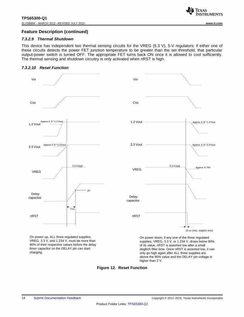
On power up, ALL three regulated supplies,VREG, 3.3 V, and 1.234 V, must be more than 90% of their respective values before the delay timer capacitor on the DELAY pin can start charging.
On power down, if any one of the three regulated supplies, VREG, 3.3 V, or 1.234 V, drops below 90% of its value, nRST is asserted low after a small deglitch filter time. Once nRST is asserted low, it can only go high again after ALL three supplies are above the 90% value and the DELAY pin voltage is higher than 2 V.
2V
TPS65300-Q1SLVSBB6F –MARCH 2012–REVISED JULY 2015 www.ti.com
Feature Description (continued)7.3.2.9 Thermal ShutdownThis device has independent two thermal sensing circuits for the VREG (5.3 V), 5-V regulators; if either one ofthese circuits detects the power FET junction temperature to be greater than the set threshold, that particularoutput-power switch is turned OFF. The appropriate FET turns back ON once it is allowed to cool sufficiently.The thermal sensing and shutdown circuitry is only activated when nRST is high.
7.3.2.10 Reset Function
Figure 12. Reset Function
14 Submit Documentation Feedback Copyright © 2012–2015, Texas Instruments Incorporated
Product Folder Links: TPS65300-Q1

TPS65300-Q1www.ti.com SLVSBB6F –MARCH 2012–REVISED JULY 2015
Feature Description (continued)7.3.3 Linear Regulators
7.3.3.1 Fixed Linear Regulator Output (5.3 V)This linear regulator is a fixed, regulated output of 5.3 V ±2% over temperature and input supply using aprecision voltage-sense resistor network. A low-ESR ceramic capacitor is required for loop stabilization; thiscapacitor must be placed close to the pin of the IC. This output is protected against shorts to ground by afoldback current limit for safe operating conditions, and a current-limit for limiting inrush current because ofdepleted charge on the output capacitor. Initial IGN_EN or EN initiates power cycle of the soft-start circuit on thisregulator. This typically is in the 1-ms to 2-ms range. This output may require a larger output capacitor to ensurethat during load transients the output does not drop below the required regulated specifications.
7.3.3.2 Fixed Linear Regulator Controller (3.3 V)The linear regulator controller requires an external NPN bipolar pass transistor of sufficient gain stage to supportthe maximum load current required. The base-drive output current is protected by current limiting both the sourceand sink drive circuitry. The 3.3VSENSE pin is the remote sense input of the output of the REG3 supply andcontrols the 3.3VDRIVE output accordingly. This regulator is a fixed 3.3-V with ±2% tolerance using a precisionvoltage-sense resistor network. A low-ESR ceramic output capacitor is used for loop compensation of theregulator. A voltage on this pin of less than approximately 50% of the regulated value initiates a current limit onthe 3.3VDRIVE output.
This output may require larger output capacitors to support load transients, so the output does not drop below90% of 3.3 V.
7.3.3.3 Fixed Linear Regulator Controller (1.2 V)The linear regulator controller requires an external NPN bipolar pass transistor of sufficient gain stage to supportthe maximum load current required. The 1.2VSENSE pin is the remote sense input of the output of 1.234-Vsupply and controls the 1.2VDRIVE output accordingly. This regulator output is 1.234 V with ±2% tolerance usinga precision voltage-sense resistor network. A low-ESR ceramic output capacitor is used for loop compensation ofthe regulator. A voltage on this pin of less than approximately 50% of the regulated value initiates a current limiton the 1.2VDRIVE output.
This output may require larger output capacitors to support load transients, so the output does not drop below90% of 1.234 V.
7.4 Device Functional Modes
7.4.1 Operational ModeThe purpose of the EN input is to keep the regulated supplies ON for a period for the microprocessor to loginformation into the memory locations when the ignition input is disabled. The microprocessor disables the powersupplies by pulling EN low after this activity is complete.
7.4.2 Buck Converter Modes of OperationThe converter operates in different modes based on load current, input voltage, and component selection.
Copyright © 2012–2015, Texas Instruments Incorporated Submit Documentation Feedback 15
Product Folder Links: TPS65300-Q1

OFF _MINLoad DS
tVREG 1 (VIN I R )
T
æ ö= - ´ - ´ç ÷ç ÷
è ø
IND _DCMSW
(1 D) VREGI
2 f L
- ´³
´ ´
IND _ CCMSW
(1 D) VREGI
2 f L
- ´³
´ ´
TPS65300-Q1SLVSBB6F –MARCH 2012–REVISED JULY 2015 www.ti.com
Device Functional Modes (continued)7.4.2.1 Continuous-Conduction Mode (CCM)This mode of operation is typically when the inductor current is non-zero and the load current is greater thanIL CCM.
where• IIND_CCM = Inductor current in continuous-conduction mode• D = duty cycle• VREG = output voltage• L = Inductor• fSW = switching frequency (4)
In this mode, the duty cycle must always be greater than the minimum tON or the converter may go into burstmode.
7.4.2.2 Discontinuous Mode (DCM)
(5)
This mode of operation is typically when the inductor current goes to zero and the load current is less thanIIND DCM.
7.4.2.3 Tracking ModeWhen the input voltage is low and the converter approaches approximately 100% duty cycle, Equation 6calculates the output voltage.
where• T = Period• RDS = Internal FET resistance• ILOAD = output load current (6)
16 Submit Documentation Feedback Copyright © 2012–2015, Texas Instruments Incorporated
Product Folder Links: TPS65300-Q1

VSENSE
GND
PH
BOOT
VIN
RT/CLK
SS
Supply
nRSTDELAY
VREG
IGN_EN
3.3VSENSE
3.3VDRIVE
Vign
BOOT_LDO
EN
IGN_ST
COMP
1.2VSENSE
1.2VDRIVE
10 µH10 µF
VIN_D
5 V
5.3 V
3.3 V
5V
1.234 V
10 µF
1nF
30 kΩ
1 µF
2.2 µF
2.2 µF
0.1 µF
2.2 µF
3 kΩ
3 kΩ
2
4
9
5
8
20
11
6
12
2123
16
17
10
18
19
15
22
14
1
3
PSS302NZ
PSS302NZ
L 5.3 W
1 W
0.48 W
1 W
0.01 µF
33 nF
40.2 kΩ
6 kΩ
5 V
5.3 V
R230 kΩ
C3470 pF
TPS65300-Q1
TPS65300-Q1www.ti.com SLVSBB6F –MARCH 2012–REVISED JULY 2015
8 Application and Implementation
NOTEInformation in the following applications sections is not part of the TI componentspecification, and TI does not warrant its accuracy or completeness. TI’s customers areresponsible for determining suitability of components for their purposes. Customers shouldvalidate and test their design implementation to confirm system functionality.
8.1 Application InformationThis section is a starting point and theoretical representation of the values to be used for the application, furtheroptimization of the components derived may be required to improve the performance of the device.
8.2 Typical Application
L: B82462G4103MOOO (EPCOS) or XFL4020 472MEB (Coilcraft)S1: MBRS310T3 (ON Semiconductors) or SS3H10 (Vishay)S2: B240A, SS16 (Vishay)External BJT: PBSS302NZ (NXP)
Figure 13. Application Schematic for a Switching Regulator
Copyright © 2012–2015, Texas Instruments Incorporated Submit Documentation Feedback 17
Product Folder Links: TPS65300-Q1
Ripple IND OI K I 0.25 1 0.25 A= ´ = ´ =
O
I
V 5.3D 0.378
V 14= = =
TPS65300-Q1SLVSBB6F –MARCH 2012–REVISED JULY 2015 www.ti.com
Typical Application (continued)8.2.1 Design RequirementsFor this design example, use the parameters listed in Table 1.
Table 1. Switching Regulator RequirementsParameter Requirement
Input voltage, VI 6.5 V to 27 V, typical 14 VOutput voltage, 5.3 V 5.3 VO ±2% at 5.3 WMaximum output current I5.3V_max 1 AMinimum output current I5.3V_min 0.01 ATransient response 0.01A to 0.8 A 5%Reset threshold 90% of output voltage5V 5VO at 1 W3.3V 3.3VO at 1 W1.234V 1.234VO at 0.5 WSwitching frequency fSW 2.5 MHzOvervoltage threshold 106% of output voltageUndervoltage threshold 95% of output voltage
8.2.2 Detailed Design ProcedureThe following design procedure provides typical application procedures as well as the details of a switchingregulator design using the requirements listed in Table 1.
8.2.2.1 Duty CycleUse Equation 7 to calculate the duty cycle.
where• VO = Output voltage• VI = Input voltage (7)
8.2.2.2 Output Inductor Selection (L)The minimum inductor value is calculated using the coefficient KIND that represents the amount of inductor ripplecurrent relative to the maximum output current. The inductor ripple current is filtered by the output capacitor, andso the typical range of this ripple current is in the range of KIND = 0.2 to 0.3, depending on the ESR and theripple-current rating of the output capacitor.
For this design example, use Equation 8 to calculate the inductor ripple current
where• IO = Output current (8)
Benefits of Low Inductor Value• Low inductor value gives high di/dt, which allows for fewer output capacitors for good load transient response.• Gives higher saturation current for the core due to fewer turns• Fewer turns yields low DCR and therefore less dc inductor losses in the windings.• High di/dt provides faster response to load steps.
Benefits of High Inductor Value• Low ripple current leads to lower conduction losses in MOSFETs• Low ripple; means lower RMS ripple current for capacitors
18 Submit Documentation Feedback Copyright © 2012–2015, Texas Instruments Incorporated
Product Folder Links: TPS65300-Q1

( )2 2O-max O-min
O _RMS 2 2 6 6O-max O-min
L (I ) (I ) 5.3 (27 5.3)I 0.049 A
(V ) (V ) 12 27 10 10 2.5 10-
- ´ -= = =
- ´ ´ ´ ´ ´
( ) ( ) ( )
( ) ( )
2 262 2O-max O-min
O 2 2 2 2O-max O-min
10 10 1 0.01L (I ) (I )C 3.18 F
(V ) (V ) 5.45 5.15
- é ù´ -- ê úë û= = = m- -
RippleL-Peak O
I 0.25I I 1 1.125 A
2 2= + = + =
I-Max O OMin 6
SW RIPPLE I-Max
(V V ) V (27 5.3) 5.3L 6.8 μH
f I V 2.5 MHz 10 0.25 27
- ´ - ´
= = =
´ ´ ´ ´ ´
TPS65300-Q1www.ti.com SLVSBB6F –MARCH 2012–REVISED JULY 2015
• Low ripple; yields low ac inductor losses in the core (flux) and windings (skin effect)• Low ripple; gives continuous inductor current flow over a wide load range
For this design example a value of 10 µH was selected because of variations in temperature and manufacture.Use Equation 9 to find the value of LMin.
where• fSW is the regulator switching frequency• IRipple = Allowable ripple current in the inductor, typically ±20% of maximum output load IO (9)
For this design example, use Equation 10 to calculate the inductor peak current.
(10)
8.2.2.3 Output Capacitor Selection (CO)The selection of the output capacitor determines several parameters in the operation of the converter, themodulator pole, the voltage droop on the out capacitor, and the output ripple.
During a load step from no load to full load or changes in the input voltage, the output capacitor must hold up theoutput voltage above a certain level for a specified time and not issue a reset until the main regulator control loopresponds to the change. The capacitance value determines the modulator pole and the roll-off frequency due tobecause of the LC output-filter double pole—the output ripple voltage is a product of the output capacitor ESRand ripple current.
Use Equation 11 to calculate the minimum capacitance required to maintain desired output voltage during a high-to-low load transition and prevent overshoot.
where• IO-max is maximum output current• IO-min is minimum output current• The difference between the output current, maximum to minimum, is the worst-case load step in the system.• VO-max is maximum tolerance of regulated output voltage• VO-min is the minimum tolerance of regulated output voltage (11)
Use Equation 12 to calculate the output capacitor root-mean-square (RMS) ripple current IO_RMS. This is toprevent excess heating or failure due to high ripple currents.
This parameter is sometimes specified by the manufacturer. Therfore, because of variations in temperature andmanufacture, use a 10-µF capacitor with a voltage rating greater than the maximum 10-V output.
(12)
Copyright © 2012–2015, Texas Instruments Incorporated Submit Documentation Feedback 19
Product Folder Links: TPS65300-Q1

I_ min OOI_RMS O
I_ min I_ min
V VV 5.3 6 5.3I I 1 0.32 A
V V 6 6
æ ö- -æ ö= ´ ´ = ´ ´ =ç ÷ ç ÷ç ÷ è øè ø
O _ maxI
I SW
I 0.25 1 0.25C 0.33 μF
V f 0.3 2.5 MHz
´ ´= = =
D ´ ´
2 2I FD SW J
D O FD
(V V ) f C (14 0.55) 2.5 MHz 30 pFP I V (1 D) 1 0.55 (1 0.378) 0.34 W
2 2
- ´ ´ - ´ ´= ´ ´ - + = ´ ´ - + =
TPS65300-Q1SLVSBB6F –MARCH 2012–REVISED JULY 2015 www.ti.com
8.2.2.4 External Schottky Diode (D)The TPS65300-Q1 device requires an external ultrafast Schottky diode with fast reverse-recovery timeconnected between the PH and power ground pins. The diode conducts the output current during the off-state ofthe internal power switch. This diode must have a reverse breakdown higher than the maximum input voltage ofthe application. A Schottky diode is selected for lower forward voltage. The Schottky diode is selected based onthe appropriate power rating, which factors in the DC-conduction losses and the AC losses because of the highswitching frequencies. The power dissipation PD is calculated with Equation 13.
where• VFD = forward conducting voltage of Schottky diode• CJ = junction capacitance of the Schottky diode (13)
8.2.2.5 Input Capacitor (CI)The TPS65300-Q1 device requires an input ceramic decoupling capacitor type X5R or X7R and bulk capacitanceto minimize input ripple voltage. The DC voltage rating of this input capacitance must be greater than themaximum input voltage. The capacitor must have an input ripple-current rating higher than the maximum inputripple current of the converter for the application. The input capacitors for power regulators are selected to havereasonable capacitance-to-volume ratio and to be fairly stable over temperature. The value of the inputcapacitance is based on the input voltage desired (∆VI).
Use Equation 14 to calculate the input capacitance.
(14)
Use Equation 15 to calculate the input-capacitor root-mean-square (RMS) ripple current II_RMS.
Because of variations in temperature and manufacture, use a 10-µF capacitor with a voltage rating greater thanthe maximum 45-V transient.
(15)
8.2.2.6 Loop CompensationThe double pole is because of the output-filter components inductor and capacitor. The calculations for thefollowing equations use values taken from Figure 14.
20 Submit Documentation Feedback Copyright © 2012–2015, Texas Instruments Incorporated
Product Folder Links: TPS65300-Q1

ESR
O
1 1f 3.2 MHz
2 C ESR 2 10 F 0.005= = =
p ´ ´ p ´ m ´
LC
O
1 1f 15.9 kHz
2 LC 2 10 H 10 F= = =
p p m ´ m
ErrorAMP
R 4 = 160.66 k R2
L
VO = VREG
Vref = 2V
xVSENSE
COMP
C
R 5 = 97.4 k
Type III Compensation
Internal compensation
C3
C 2 = 20pfC 4 = 140pf
R 3 = 8 k
CESR
CO
x
x
Internal Resistor Divider
TPS65300-Q1www.ti.com SLVSBB6F –MARCH 2012–REVISED JULY 2015
8.2.2.7 Loop-Control Frequency Compensation
Figure 14. Loop-Control Frequency Compensation
8.2.2.7.1 Type III Compensation
fCO = fSW × 0.1 (the cutoff frequency when the gain is 1 is called the unity-gain frequency).
fCO is typically 1/5 to 1/10 of the switching frequency double-pole frequency response due to the LC output filter.The LC output filter gives a double pole, which has a –180° phase shift.
Make the two zeroes close to the double pole (LC), for example, fZ1 ≈ fZ2 ≈ 1/2π(LCOUT)1/2.1. Make the first zero below the filter double pole (approximately 50% to 75% of fLC)2. Make the second zero at the filter double pole (fLC)
Make the two poles above the crossover frequency fCO.3. Make the first pole at the ESR frequency (fESR)4. Make the second pole at 0.5 the switching frequency
The following compensation components are integrated in the device with the following typical values. Guidelinesfor compensation components:
R3 = 8 kΩ, C4 = 140 pF, C2 = 20 pF
Use Equation 16 to calculate the double pole to calculate the output filter components LC.
(16)
The ESR of the output capacitor C gives a zero that has a 90° phase shift. The ESR of the output capacitor mustbe in the range of 1 mΩ to 100 mΩ. Use Equation 17 to calculate the value of fESR.
(17)
Copyright © 2012–2015, Texas Instruments Incorporated Submit Documentation Feedback 21
Product Folder Links: TPS65300-Q1

P1
P2
Z1
Z2
1 1f 31.6 kHz
2 R2 C2 2 251.6 k 20 pF
1 1f 142.1 kHz
2 R3 C4 2 8 k 140 pF
1 1f 7.91 kHz
2 R2 C3 2 251.6 k 80 pF
1 1f 7.07 kHz
2 R4 C4 2 160.7 k 140 pF
= = =p ´ ´ p ´ W ´
= = =p ´ ´ p ´ W ´
= = =p ´ ´ p ´ W ´
= = =p ´ ´ p ´ W ´
V
R2 (R4 R3)A
(R4 R3)
´ +=
´
LC
1 1C3 80 pF
R2 f 251.6 k 15.9 kHz= = =
p ´ ´ p ´ W ´
CO ramp
LC I
f V R4 250 kHz 1.4 160 kR2 251.6 k
f V 15.9 kHz 14
´ ´ ´ ´ W= = = W
´ ´
OR5 (V Vref ) 97.4 k (5.3 2)R4 160.7 k
Vref 2
´ - W ´ -= = = W
I
ramp
VK
V=
TPS65300-Q1SLVSBB6F –MARCH 2012–REVISED JULY 2015 www.ti.com
8.2.2.7.2 PWM Modulator Gain K
where• Vramp = VI / 10, VI = Input operating voltage (18)
8.2.2.7.3 Resistor Values
In this design example, select a value of 97.4 k Ω for R5 and use Equation 19 to calculate the value of R4.
where• Vref = 2 V (19)
Use Equation 20 to calculate the value of R2 for this design example.
(20)
Calculate C3 based on placing a zero at 50% to 75% of the output-filter double-pole frequency (below set at50%).
For this design example, use Equation 21 to calculate the value of C3 as 80 pF.
(21)
8.2.2.7.4 Gain of Amplifier
(22)
8.2.2.7.5 Poles and Zero Frequencies
The following equations were used in this design example:
(23)
22 Submit Documentation Feedback Copyright © 2012–2015, Texas Instruments Incorporated
Product Folder Links: TPS65300-Q1

Modulator Gain
Open Loop ErrorAmp Gain
Closed Loop Gain
Compensation
Gain
fZ2fZ1 fP1 fP2
fLCo fESR
Frequency
Ga
in(d
B)
TPS65300-Q1www.ti.com SLVSBB6F –MARCH 2012–REVISED JULY 2015
Figure 15. Typical Gain Versus Frequency
8.2.2.8 Power Dissipation
8.2.2.8.1 Switch-Mode Power-Supply Losses
The power dissipation losses are applicable for continuous-conduction mode operation (CCM).1. Conduction losses
P5.3V_CON = IO2 × Rds(on) × (VO/VI)
where• IO = Output current• VO = VREG = Output voltage• VI = Input voltage• fSW = Switching frequency (24)
2. Switching lossesP5.3V_SW = ½ × VI × IO × (tr + tf) × fSW
where• tr = FET switching rise time (tr max = 20 ns)• tf = FET switching fall time (tf max = 20 ns) (25)
3. Gate drive lossesP5.3V_Gate = Vdrive × Qg × fSW
where• Vdrive = FET gate-drive voltage (typically Vdrive = 6 V and Vdrive max = 8 V)• Qg = 1 × 10⁻⁹ (nC) (typical) (26)
4. Supply lossesPIC = VI × Iq-normal (27)
Therefore:PTotal = PCON + PSW + PGate + P5V_Lin Reg + PIC (28)
Copyright © 2012–2015, Texas Instruments Incorporated Submit Documentation Feedback 23
Product Folder Links: TPS65300-Q1

2 25.3V _ CON O ds(on) O I
5.3V _ SW I O r f SW
9 9 6
9 65.3V _ Gate drive SW
5V _Lin Reg O
P I r (V / V ) 1 0.5 (5.3 / 14) 0.189 W
P 1/ 2 V I (t t ) f
1/ 2 14 1 (20 10 20 10 ) 2.5 10 0.7 W
P V Qg f 8 1 10 2.5 10 0.02 W
P (VREG 5V) I (5.3 5.
- -
-
= ´ ´ = ´ ´ =
= ´ ´ ´ + ´
= ´ ´ ´ ´ + ´ ´ ´ =
= ´ ´ = ´ ´ ´ ´ =
= - ´ = -
IC I IC
Total 5.3V _ CON 5.3V _ SW 5.3V _ Gate 5V _Lin Reg IC
0) 0.2 0.06 W
P V I 14 5 mA 0.07 W
P P P P P P
0.189 0.7 0.02 0.06 0.07 1.039 W
´ =
= ´ = ´ =
= + + + +
= + + + + =
TPS65300-Q1SLVSBB6F –MARCH 2012–REVISED JULY 2015 www.ti.com
P5V_Lin Reg = (VREG – 5 V) × IO (29)
Therefore, for this design, the following equations were used:
(30)
For given operating ambient temperature TATJ = TA + Rth × PTotal
where• TJ = Junction temperature in °C• TA = Ambient temperature in °C• PTotal = Total power dissipation (watts) (31)
For a given max junction temperature TJ-Max = 150°CTA-Max = TJ-Max – Rth × PTotal
where• TA-Max = Maximum ambient temperature in °C• TJ-Max = Maximum junction temperature in °C• Rth = Thermal resistance of package in (°C/W) (32)
Other factors not included in the foregoing information which affect the overall efficiency and power losses are• Inductor AC and DC losses• Trace resistance and losses associated with the copper trace routing connection• Schottky diode
24 Submit Documentation Feedback Copyright © 2012–2015, Texas Instruments Incorporated
Product Folder Links: TPS65300-Q1

A004 A003
0
0.2
0.4
0.6
0.8
1
0 200 400 600 800 1000 1200
Output Current (mA)
Effic
ien
cy
G001
Vreg=5Fsw=2245 kHzL=10 uHCo=10 uF
Vin = 7 VVin = 12 V
A002
JESD51-5
45 80 115 150
1.0
2.0
3.0
Ambient Temperature (°C)
Pow
er
Dis
sip
ation (
W)
TPS65300-Q1www.ti.com SLVSBB6F –MARCH 2012–REVISED JULY 2015
Figure 16. Power Dissipation Derating Profile, 24-Pin PWP Package With Thermal Pad
8.2.3 Application Curves
Figure 18. Load Transient Response, 10 mA to 200 mAFigure 17. Efficiency vs Output Current on VREG
Figure 19. Load Transient Response, 10 mA to 350 mA Figure 20. Load Transient Response, 10 mA to 550 mA
Copyright © 2012–2015, Texas Instruments Incorporated Submit Documentation Feedback 25
Product Folder Links: TPS65300-Q1

A001
TPS65300-Q1SLVSBB6F –MARCH 2012–REVISED JULY 2015 www.ti.com
Figure 21. Load Transient Response, 10 mA to 1 A
9 Power Supply RecommendationsThe TPS65300-Q1 device is designed to operate using an input supply voltage range from 5.6 V to 40 V.
10 Layout
10.1 Layout GuidelinesThe following guidelines are recommended for the printed circuit board (PCB) layout of the TPS65300-Q1device.
10.1.1 Inductor LUse a low-EMI inductor with a ferrite-type shielded core. Other types of inductors may be used; however, theymust have low-EMI characteristics and be located away from the low-power traces and components in the circuit.
10.1.2 Input Filter Capacitors CI
Input ceramic filter capacitors should be located in close proximity to the VIN pin. Surface-mount capacitors arerecommended to minimize lead length and reduce noise coupling.
10.1.3 FeedbackRoute the feedback trace such that there is minimum interaction with any noise sources associated with theswitching components. Recommended practice is to ensure placing the inductor away from the feedback trace toprevent a source of EMI noise.
10.1.4 Traces and Ground PlaneAll power (high-current) traces should be thick and as short as possible. The inductor and output capacitorsshould be as close to each other as possible. This reduces EMI radiated by the power traces due to highswitching currents.
In a two-sided PCB it is recommended to have ground planes on both sides of the PCB to help reduce noise andground-loop errors. The ground connection for the input and output capacitors and IC ground should beconnected to this ground plane.
In a multi-layer PCB, the ground plane is used to separate the power plane (where high switching currents andcomponents are placed) from the signal plane (where the feedback trace and components are) for improvedperformance.
Also arrange the components such that the switching-current loops curl in the same direction. Place the high-current components such that during conduction the current path is in the same direction. This prevents magneticfield reversal caused by the traces between the two half-cycles, helping to reduce radiated EMI.
26 Submit Documentation Feedback Copyright © 2012–2015, Texas Instruments Incorporated
Product Folder Links: TPS65300-Q1

PH
BOOT
VIN
VREG
EN
10 µF
VIN_D
10 µF
S1
S2
1 nF 6 k 30 k
R2
2.2 µF
2.2 µF
0.1 µF
C3
3 k
3 k
1
L
2
3
4
IGN_EN5
6
7
8
9
RT/CLK
NC
BOOT_LDO
5V10
IGN_ST11
1 µF
2.2 µF
GND12 13NC
14COMP
15VSENSE
16
17
1.2VSENSE
1.2VDRIVE
183.3VSENSE
3.3VDRIVE 19
20SS
21DELAY
22
23nRST
24PGND
T1
T2
Exposed PAD Connected to Ground Plane
Connection to backside of PCB through vias
Connection to topside of PCB through vias
Connection to ground plane of PCB through vias
Power bus
Voltage Output rails
T1, T2 are PSS302NZ, sufficent heat sink may be required for power dissipation
5.3 V
Supply
VignEnable
IGN_ST
1.234 V5 V
3.3 V
TPS65300-Q1
R1
C1
C2
nRST
TPS65300-Q1www.ti.com SLVSBB6F –MARCH 2012–REVISED JULY 2015
10.2 Layout Example
Figure 22. PCB Layout
Copyright © 2012–2015, Texas Instruments Incorporated Submit Documentation Feedback 27
Product Folder Links: TPS65300-Q1

TPS65300-Q1SLVSBB6F –MARCH 2012–REVISED JULY 2015 www.ti.com
11 Device and Documentation Support
11.1 Device Support
11.1.1 Third-Party Products DisclaimerTI'S PUBLICATION OF INFORMATION REGARDING THIRD-PARTY PRODUCTS OR SERVICES DOES NOTCONSTITUTE AN ENDORSEMENT REGARDING THE SUITABILITY OF SUCH PRODUCTS OR SERVICESOR A WARRANTY, REPRESENTATION OR ENDORSEMENT OF SUCH PRODUCTS OR SERVICES, EITHERALONE OR IN COMBINATION WITH ANY TI PRODUCT OR SERVICE.
11.2 Documentation Support
11.2.1 Related DocumentationFor related documentation see the following:
User's Guide, TPS65300EVM, SLVU685
11.3 Community ResourceThe following links connect to TI community resources. Linked contents are provided "AS IS" by the respectivecontributors. They do not constitute TI specifications and do not necessarily reflect TI's views; see TI's Terms ofUse.
TI E2E™ Online Community TI's Engineer-to-Engineer (E2E) Community. Created to foster collaborationamong engineers. At e2e.ti.com, you can ask questions, share knowledge, explore ideas and helpsolve problems with fellow engineers.
Design Support TI's Design Support Quickly find helpful E2E forums along with design support tools andcontact information for technical support.
11.4 TrademarksPowerPAD, E2E are trademarks of Texas Instruments.All other trademarks are the property of their respective owners.
11.5 Electrostatic Discharge CautionThis integrated circuit can be damaged by ESD. Texas Instruments recommends that all integrated circuits be handled withappropriate precautions. Failure to observe proper handling and installation procedures can cause damage.
ESD damage can range from subtle performance degradation to complete device failure. Precision integrated circuits may be moresusceptible to damage because very small parametric changes could cause the device not to meet its published specifications.
11.6 GlossarySLYZ022 — TI Glossary.
This glossary lists and explains terms, acronyms, and definitions.
12 Mechanical, Packaging, and Orderable InformationThe following pages include mechanical packaging and orderable information. This information is the mostcurrent data available for the designated devices. This data is subject to change without notice and revision ofthis document. For browser-based versions of this data sheet, refer to the left-hand navigation.
28 Submit Documentation Feedback Copyright © 2012–2015, Texas Instruments Incorporated
Product Folder Links: TPS65300-Q1

PACKAGE OPTION ADDENDUM
www.ti.com 16-Jun-2015
Addendum-Page 1
PACKAGING INFORMATION
Orderable Device Status(1)
Package Type PackageDrawing
Pins PackageQty
Eco Plan(2)
Lead/Ball Finish(6)
MSL Peak Temp(3)
Op Temp (°C) Device Marking(4/5)
Samples
TPS65300QPWPRQ1 ACTIVE HTSSOP PWP 24 2000 Green (RoHS& no Sb/Br)
CU NIPDAU Level-3-260C-168 HR -40 to 125 TPS65300
TPS65300QRHFRQ1 ACTIVE VQFN RHF 24 3000 Green (RoHS& no Sb/Br)
CU NIPDAU Level-3-260C-168 HR -40 to 125 65300Q1
(1) The marketing status values are defined as follows:ACTIVE: Product device recommended for new designs.LIFEBUY: TI has announced that the device will be discontinued, and a lifetime-buy period is in effect.NRND: Not recommended for new designs. Device is in production to support existing customers, but TI does not recommend using this part in a new design.PREVIEW: Device has been announced but is not in production. Samples may or may not be available.OBSOLETE: TI has discontinued the production of the device.
(2) Eco Plan - The planned eco-friendly classification: Pb-Free (RoHS), Pb-Free (RoHS Exempt), or Green (RoHS & no Sb/Br) - please check http://www.ti.com/productcontent for the latest availabilityinformation and additional product content details.TBD: The Pb-Free/Green conversion plan has not been defined.Pb-Free (RoHS): TI's terms "Lead-Free" or "Pb-Free" mean semiconductor products that are compatible with the current RoHS requirements for all 6 substances, including the requirement thatlead not exceed 0.1% by weight in homogeneous materials. Where designed to be soldered at high temperatures, TI Pb-Free products are suitable for use in specified lead-free processes.Pb-Free (RoHS Exempt): This component has a RoHS exemption for either 1) lead-based flip-chip solder bumps used between the die and package, or 2) lead-based die adhesive used betweenthe die and leadframe. The component is otherwise considered Pb-Free (RoHS compatible) as defined above.Green (RoHS & no Sb/Br): TI defines "Green" to mean Pb-Free (RoHS compatible), and free of Bromine (Br) and Antimony (Sb) based flame retardants (Br or Sb do not exceed 0.1% by weightin homogeneous material)
(3) MSL, Peak Temp. - The Moisture Sensitivity Level rating according to the JEDEC industry standard classifications, and peak solder temperature.
(4) There may be additional marking, which relates to the logo, the lot trace code information, or the environmental category on the device.
(5) Multiple Device Markings will be inside parentheses. Only one Device Marking contained in parentheses and separated by a "~" will appear on a device. If a line is indented then it is a continuationof the previous line and the two combined represent the entire Device Marking for that device.
(6) Lead/Ball Finish - Orderable Devices may have multiple material finish options. Finish options are separated by a vertical ruled line. Lead/Ball Finish values may wrap to two lines if the finishvalue exceeds the maximum column width.
Important Information and Disclaimer:The information provided on this page represents TI's knowledge and belief as of the date that it is provided. TI bases its knowledge and belief on informationprovided by third parties, and makes no representation or warranty as to the accuracy of such information. Efforts are underway to better integrate information from third parties. TI has taken andcontinues to take reasonable steps to provide representative and accurate information but may not have conducted destructive testing or chemical analysis on incoming materials and chemicals.TI and TI suppliers consider certain information to be proprietary, and thus CAS numbers and other limited information may not be available for release.

PACKAGE OPTION ADDENDUM
www.ti.com 16-Jun-2015
Addendum-Page 2
In no event shall TI's liability arising out of such information exceed the total purchase price of the TI part(s) at issue in this document sold by TI to Customer on an annual basis.

TAPE AND REEL INFORMATION
*All dimensions are nominal
Device PackageType
PackageDrawing
Pins SPQ ReelDiameter
(mm)
ReelWidth
W1 (mm)
A0(mm)
B0(mm)
K0(mm)
P1(mm)
W(mm)
Pin1Quadrant
TPS65300QPWPRQ1 HTSSOP PWP 24 2000 330.0 16.4 6.95 8.3 1.6 8.0 16.0 Q1
TPS65300QRHFRQ1 VQFN RHF 24 3000 330.0 12.4 4.3 5.3 1.3 8.0 12.0 Q1
PACKAGE MATERIALS INFORMATION
www.ti.com 16-Jun-2015
Pack Materials-Page 1
*All dimensions are nominal
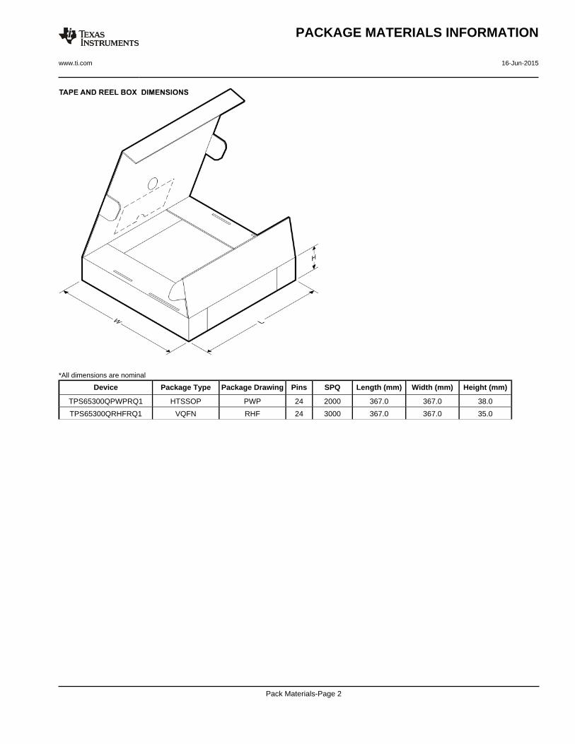
Device Package Type Package Drawing Pins SPQ Length (mm) Width (mm) Height (mm)
TPS65300QPWPRQ1 HTSSOP PWP 24 2000 367.0 367.0 38.0
TPS65300QRHFRQ1 VQFN RHF 24 3000 367.0 367.0 35.0
PACKAGE MATERIALS INFORMATION
www.ti.com 16-Jun-2015
Pack Materials-Page 2


IMPORTANT NOTICE
Texas Instruments Incorporated and its subsidiaries (TI) reserve the right to make corrections, enhancements, improvements and otherchanges to its semiconductor products and services per JESD46, latest issue, and to discontinue any product or service per JESD48, latestissue. Buyers should obtain the latest relevant information before placing orders and should verify that such information is current andcomplete. All semiconductor products (also referred to herein as “components”) are sold subject to TI’s terms and conditions of salesupplied at the time of order acknowledgment.TI warrants performance of its components to the specifications applicable at the time of sale, in accordance with the warranty in TI’s termsand conditions of sale of semiconductor products. Testing and other quality control techniques are used to the extent TI deems necessaryto support this warranty. Except where mandated by applicable law, testing of all parameters of each component is not necessarilyperformed.TI assumes no liability for applications assistance or the design of Buyers’ products. Buyers are responsible for their products andapplications using TI components. To minimize the risks associated with Buyers’ products and applications, Buyers should provideadequate design and operating safeguards.TI does not warrant or represent that any license, either express or implied, is granted under any patent right, copyright, mask work right, orother intellectual property right relating to any combination, machine, or process in which TI components or services are used. Informationpublished by TI regarding third-party products or services does not constitute a license to use such products or services or a warranty orendorsement thereof. Use of such information may require a license from a third party under the patents or other intellectual property of thethird party, or a license from TI under the patents or other intellectual property of TI.Reproduction of significant portions of TI information in TI data books or data sheets is permissible only if reproduction is without alterationand is accompanied by all associated warranties, conditions, limitations, and notices. TI is not responsible or liable for such altereddocumentation. Information of third parties may be subject to additional restrictions.Resale of TI components or services with statements different from or beyond the parameters stated by TI for that component or servicevoids all express and any implied warranties for the associated TI component or service and is an unfair and deceptive business practice.TI is not responsible or liable for any such statements.Buyer acknowledges and agrees that it is solely responsible for compliance with all legal, regulatory and safety-related requirementsconcerning its products, and any use of TI components in its applications, notwithstanding any applications-related information or supportthat may be provided by TI. Buyer represents and agrees that it has all the necessary expertise to create and implement safeguards whichanticipate dangerous consequences of failures, monitor failures and their consequences, lessen the likelihood of failures that might causeharm and take appropriate remedial actions. Buyer will fully indemnify TI and its representatives against any damages arising out of the useof any TI components in safety-critical applications.In some cases, TI components may be promoted specifically to facilitate safety-related applications. With such components, TI’s goal is tohelp enable customers to design and create their own end-product solutions that meet applicable functional safety standards andrequirements. Nonetheless, such components are subject to these terms.No TI components are authorized for use in FDA Class III (or similar life-critical medical equipment) unless authorized officers of the partieshave executed a special agreement specifically governing such use.Only those TI components which TI has specifically designated as military grade or “enhanced plastic” are designed and intended for use inmilitary/aerospace applications or environments. Buyer acknowledges and agrees that any military or aerospace use of TI componentswhich have not been so designated is solely at the Buyer's risk, and that Buyer is solely responsible for compliance with all legal andregulatory requirements in connection with such use.TI has specifically designated certain components as meeting ISO/TS16949 requirements, mainly for automotive use. In any case of use ofnon-designated products, TI will not be responsible for any failure to meet ISO/TS16949.
Products ApplicationsAudio www.ti.com/audio Automotive and Transportation www.ti.com/automotiveAmplifiers amplifier.ti.com Communications and Telecom www.ti.com/communicationsData Converters dataconverter.ti.com Computers and Peripherals www.ti.com/computersDLP® Products www.dlp.com Consumer Electronics www.ti.com/consumer-appsDSP dsp.ti.com Energy and Lighting www.ti.com/energyClocks and Timers www.ti.com/clocks Industrial www.ti.com/industrialInterface interface.ti.com Medical www.ti.com/medicalLogic logic.ti.com Security www.ti.com/securityPower Mgmt power.ti.com Space, Avionics and Defense www.ti.com/space-avionics-defenseMicrocontrollers microcontroller.ti.com Video and Imaging www.ti.com/videoRFID www.ti-rfid.comOMAP Applications Processors www.ti.com/omap TI E2E Community e2e.ti.comWireless Connectivity www.ti.com/wirelessconnectivity
Mailing Address: Texas Instruments, Post Office Box 655303, Dallas, Texas 75265Copyright © 2016, Texas Instruments Incorporated


![sbRIO-9628 Specifications - National Instruments · FPGA_VIO [48-95] 2.5 V/3.3 V Power Selector 2.5 V/3.3 V Power Selector RMC Connector earay) Table 1. CompactRIO Single Board Controller](https://img.pdfslide.us/doc/110x75/5f6eb2fe4b12a30ba3558804/sbrio-9628-specifications-national-fpgavio-48-95-25-v33-v-power-selector.jpg)