Embed Size (px)
Citation preview

FEATURES
Controlled Baseline− One Assembly/Test Site, One Fabrication
Site
Extended Temperature Performance of Up to−55°C to +125°C
Enhanced Diminishing ManufacturingSources (DMS) Support
Enhanced Product-Change Notification
Qualification Pedigree (1)
Single Voltage Detector (TPS3803):Adjustable/1.5 V
Dual Voltage Detector (TPS3805):Adjustable/3.3 V
High ±1.5% Threshold Voltage Accuracy
Supply Current: 3 µA Typical at V DD = 3.3 V
Push/Pull Reset Output (TPS3805) Open-DrainReset Output (TPS3803)
5-Pin SC−70 Package(1) Component qualification in accordance with JEDEC and industry
standards to ensure reliable operation over an extendedtemperature range. This includes, but is not limited to, HighlyAccelerated Stress Test (HAST) or biased 85/85, temperaturecycle, autoclave or unbiased HAST, electromigration, bondintermetallic life, and mold compound life. Such qualificationtesting should not be viewed as justifying use of this componentbeyond specified performance and environmental limits.
APPLICATIONS
Applications Using DSPs, Microcontrollers,or Microprocessors
Wireless Communication Systems
Portable/Battery-Powered Equipment
Programmable Controls
Intelligent Instruments
Industrial Equipment
Notebook/Desktop Computers
Automotive Systems
DESCRIPTION
The TPS3803 and TPS3805 families of supervisory circuitsprovide circuit initialization and timing supervision, primarilyfor DSPs and processor-based systems.
The TPS3803G15 device has a fixed-sense threshold voltageVIT set by an internal voltage divider, whereas theTPS3803−01 has an adjustable SENSE input that can beconfigured by two external resistors. In addition to the fixedsense threshold monitored at VDD, the TPS3805 devicesprovide a second adjustable SENSE input. RESET isasserted in case any of the two voltages drops below VIT.
During power on, RESET is asserted when supply voltageVDD becomes higher than 0.8 V. Thereafter, the supervisorycircuit monitors VDD (and/or SENSE) and keeps RESETactive as long as VDD or SENSE remains below the thresholdvoltage VIT. As soon as VDD (SENSE) rises above thethreshold voltage VIT, RESET is deasserted again. Theproduct spectrum is designed for 1.5 V, 3.3 V, and adjustablesupply voltages. The devices are available in a 5-pin SC-70package.
3
2
4
5
DCK PACKAGE(Top View)
1NC
GND
RESET
(1) NC = No Connection on TPS3803G15
VDD
SENSENC(1)
TPS3803−01, TPS3803G15, TPS3805
Typical Operating Circuit
TPS3805H33 TMS320VC5416
RESETVDD
SENSE GND
DVDD CVDD
RESET
GND
3.3 V1.6 V
R1
R2
www.ti.com
TPS3803-01-EPTPS3803G15-EPTPS3805H33-EP
SGLS227C − DECEMBER 2003 − REVISED JUNE 2007
VOLTAGEDETECTOR
! !
www.ti.com
Copyright 2003−2007, Texas Instruments Incorporated
Please be aware that an important notice concerning availability, standard warranty, and use in critical applications of Texas Instrumentssemiconductor products and disclaimers thereto appears at the end of this data sheet.
All trademarks are the property of their respective owners.

"#$%#&%'&("#$%#)'*&("#$%*+##&(SGLS227C − DECEMBER 2003 − REVISED JUNE 2007
www.ti.com
2
This integrated circuit can be damaged by ESD. Texas Instruments recommends that all integrated circuits be handled withappropriate precautions. Failure to observe proper handling and installation procedures can cause damage.
ESD damage can range from subtle performance degradation to complete device failure. Precision integrated circuits may be more susceptibleto damage because very small parametric changes could cause the device not to meet its published specifications.
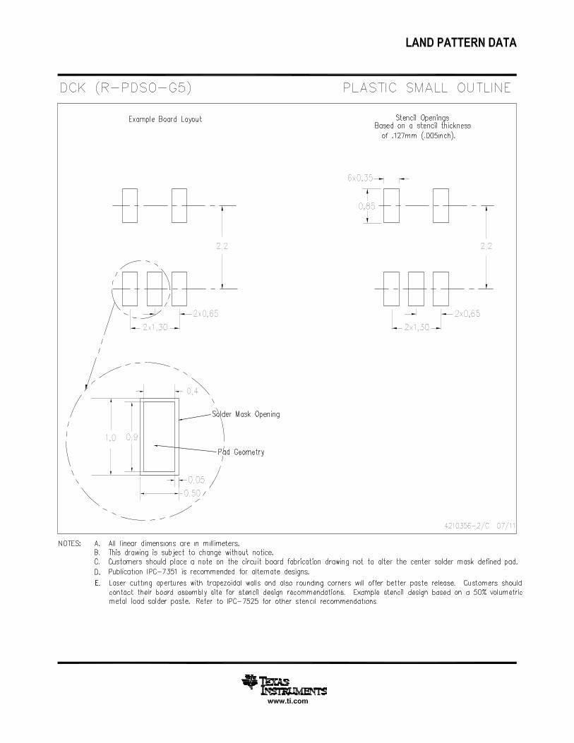
PACKAGE INFORMATION
TA DEVICE NAMETHRESHOLD VOLTAGE
MARKINGTA DEVICE NAMEVDD SENSE
MARKING
TPS3803−01QDCKREP(2) NA 1.226 V AWH
−40C to +125C TPS3803G15QDCKREP(2) 1.4 V NA AXT−40 C to +125 C
TPS3805H33QDCKREP(2) 3.05 V 1.226 V AWY
TPS3803−01MDCKREP(2) NA 1.226 V BAY
−55C to +125C TPS3803G15MDCKREP(2) 1.40 V NA ARH−55 C to +125 C
TPS3805H33MDCKREP(2) 3.05 V 1.226 V ARJ(2) The DCKR passive indicates tape and reel containing 3000 parts.
ORDERING INFORMATION
TPS380 3 G 15 DCK R
ReelPackage
Nominal Supply VoltageNominal Threshold Voltage
FunctionalityFamily
Q
Temperature Designator
EP
Enhanced Plastic Designator
Function/Truth TablesTPS3803-01 TPS3803G15
SENSE > VIT RESET VDD > VIT RESET
0 L 0 L
1 H 1 H
TPS3805H33
VDD > VIT SENSE > VIT RESET
0 0 L
0 1 L
1 0 L
1 1 H

"#$%#&%'&("#$%#)'*&("#$%*+##&(
SGLS227C − DECEMBER 2003 − REVISED JUNE 2007
www.ti.com
3
FUNCTIONAL BLOCK DIAGRAM
_
+
R1
R2
ReferenceVoltage
of 1.215 V
TPS3803G15
RESETVDD
GND
_
+
ReferenceVoltage
of 1.226 V
TPS3803−01
RESET
VDD
GND
SENSE
DeviceSupply Voltage
_
+
_
+
R1
R2
VDD
GND
ReferenceVoltage
of 1.226 V
SENSE
RESET
TPS3805

"#$%#&%'&("#$%#)'*&("#$%*+##&(SGLS227C − DECEMBER 2003 − REVISED JUNE 2007
www.ti.com
4
TIMING REQUIREMENTSVDD or SENSE
VIT + VhysVIT
0.8 V
RESET
= Undefined
Terminal FunctionsTERMINAL
I/O DESCRIPTIONNAME NO.
I/O DESCRIPTION
GND 2 I Ground
RESET 3 O Active-low reset output (TPS3803—open-drain, TPS3805—push/pull)
SENSE 5 I Adjustable sense input
NC 1 No internal connection
NC (TPS3803G15) 5 No internal connection
VDD 4 I Input supply voltage, fixed sense input for TPS3803G15 and TPS3805

"#$%#&%'&("#$%#)'*&("#$%*+##&(
SGLS227C − DECEMBER 2003 − REVISED JUNE 2007
www.ti.com
5
ABSOLUTE MAXIMUM RATINGS (1)
Over operating free-air temperature, unless otherwise noted.
Supply voltage, VDD(2) +7 V. . . . . . . . . . . . . . . . . . . . . . . . . . . . . . . . . . . . . . . . . . . . . . . . . . . . . . . . . . . . . . . . . . . . . . All other pins(2) −0.3 V to +7 V. . . . . . . . . . . . . . . . . . . . . . . . . . . . . . . . . . . . . . . . . . . . . . . . . . . . . . . . . . . . . . . . . . . . Maximum low-output current, IOL +5 mA. . . . . . . . . . . . . . . . . . . . . . . . . . . . . . . . . . . . . . . . . . . . . . . . . . . . . . . . . . . Maximum high-output current, IOH −5 mA. . . . . . . . . . . . . . . . . . . . . . . . . . . . . . . . . . . . . . . . . . . . . . . . . . . . . . . . . . Input clamp current, IIK (VI < 0 or VI > VDD) ±10 mA. . . . . . . . . . . . . . . . . . . . . . . . . . . . . . . . . . . . . . . . . . . . . . . . . Output clamp current, IOK (VO < 0 or VO > VDD) ±10 mA. . . . . . . . . . . . . . . . . . . . . . . . . . . . . . . . . . . . . . . . . . . . Continuous total power dissipation See Dissipation Rating Table. . . . . . . . . . . . . . . . . . . . . . . . . . . . . . . . . . . . . . Operating free-air temperature range, TA −55°C to +125°C. . . . . . . . . . . . . . . . . . . . . . . . . . . . . . . . . . . . . . . . . . . Storage temperature range, Tstg,(3) −65°C to +150°C. . . . . . . . . . . . . . . . . . . . . . . . . . . . . . . . . . . . . . . . . . . . . . . .
(1) Stresses beyond those listed under “absolute maximum ratings” may cause permanent damage to the device. These are stress ratings only,and functional operation of the device at these or any other conditions beyond those indicated under “recommended operating conditions” isnot implied. Exposure to absolute-maximum-rated conditions for extended periods may affect device reliability.
(2) All voltage values are with respect to GND. For reliable operation the device should not be continuously operated at 7 V for more thant = 1000 h.
(3) Long-term high-temperature storage and/or extended use at maximum recommended operating conditions may result in a reduction of overalldevice life. See www.ti.com/ep_quality for additional information on enhanced plastic packaging.
DISSIPATION RATING TABLE
PACKAGE TA < +25°CPOWER RATING
DERATING FACTORABOVE TA = +25°C
TA = +70°CPOWER RATING
TA = +85°CPOWER RATING
DCK 321 mW 2.6 mW/°C 206 mW 167 mW
RECOMMENDED OPERATING CONDITIONSMIN MAX UNIT
Supply voltage, VDD 1.3 6 V
Input voltage, VI 0 VDD + 0.3 V
Operating free-air temperature range, TAQ suffix devices −40 +125
°COperating free-air temperature range, TAM suffix devices −55 +125
°C

"#$%#&%'&("#$%#)'*&("#$%*+##&(SGLS227C − DECEMBER 2003 − REVISED JUNE 2007
www.ti.com
6
ELECTRICAL CHARACTERISTICSOver recommended operating free-air temperature range, unless otherwise noted.
PARAMETER TEST CONDITIONS MIN TYP MAX UNIT
VDD = 1.5 V, IOH = −0.5 mA
VOH High-level output voltage (TPS3805 only) VDD = 3.3 V, IOH = −1 mA 0.8 x VDD VVOH High-level output voltage (TPS3805 only)
VDD = 6 V, IOH = −1.5 mA
0.8 x VDD V
VDD = 1.5 V, IOL = 1 mA
VOL Low-level output voltage VDD = 3.3 V, IOL = 2 mA 0.3 VVOL Low-level output voltage
VDD = 6 V, IOL = 3 mA
0.3 V
Power-up reset voltage(1)VIT > 1.5 V, TA = +25°C 0.8 V
Power-up reset voltage(1)VIT ≤ 1.5 V, TA = +25°C 1 V
Negative-going input thresholdSENSE 1.2 1.226 1.244
VITNegative-going input thresholdvoltage(2) TPS3803G15 1.379 1.4 1.421 VVIT voltage(2)
TPS3805H33 3.004 3.05 3.096
V
Vhys Hysteresis1.2 V < VIT < 2.5 V 15
mVVhys Hysteresis2.5 V < VIT < 3.5 V 30
mV
II Input current SENSE −25 25 nA
IOH High-level output current at RESET Open-drain only VDD = VIT + 0.2V, VOH = VDD 300 nA
TPS3803−01 2 4
IDD Supply current
TPS3805,TPS3803G15
VDD = 3.3 V, output unconnected3 5
AIDD Supply currentTPS3803−01 2 4
µA
TPS3805,TPS3803G15
VDD = 6 V, output unconnected4 6
CI Input capacitance VI = 0 V to VDD 1 pF
(1) The lowest supply voltage at which RESET (VOL(max) = 0.2 V, IOL = 50 µA) becomes active. tr(VDD) ≥ 15 µs/V(2) To ensure the best stability of the threshold voltage, place a bypass capacitor (ceramic, 0.1 µF) near the supply terminals.
TIMING REQUIREMENTSAT RL = 1 MΩ, CL = 50 PF, over recommended operating free-air temperature range.
PARAMETER TEST CONDITIONS MIN TYP MAX UNIT
tw Pulse widthAt VDD
VIH = 1.05 x VIT, VIL = 0.95 x VIT 5.5 stw Pulse widthAt SENSE
VIH = 1.05 x VIT, VIL = 0.95 x VIT 5.5 µs
SWITCHING CHARACTERISTICSAT RL = 1 MΩ, CL = 50 PF, over recommended operating free-air temperature range.
PARAMETER TEST CONDITIONS MIN TYP MAX UNIT
tPHLPropagation (delay) time, VDD to RESET delay
V = 1.05 x V , 5 100tPHLPropagation (delay) time,high-to-low-level output SENSE to RESET delay VIH = 1.05 x VIT,
VIL = 0.95 x VIT
5 100
s
tPLHPropagation (delay) time, VDD to RESET delay
IH ITVIL = 0.95 x VIT
5 100
µs
tPLHPropagation (delay) time,low-to-high-level output SENSE to RESET delay
5 100

"#$%#&%'&("#$%#)'*&("#$%*+##&(
SGLS227C − DECEMBER 2003 − REVISED JUNE 2007
www.ti.com
7
TYPICAL CHARACTERISTICS
Figure 1
3
2
1
00 0.5 1 1.5 2 2.5 3
4
5
TPS3805H33SUPPLY CURRENT
vsSUPPLY VOLTAGE
6
3.5 4 4.5 5 5.5 6
DD
IS
uppl
y C
urre
nt −
−
Aµ
VDD − Supply Voltage − V
SENSE = GNDRESET = Open
85°C
0°C
25°C
−40°C
Figure 2
1.5
1
0.5
00 0.5 1 1.5 2 2.5 3
2
2.5
TPS3803−01SUPPLY CURRENT
vsSUPPLY VOLTAGE
3
3.5 4 4.5 5 5.5 6
DD
IS
uppl
y C
urre
nt −
−
Aµ
VDD − Supply Voltage − V
SENSE = GNDRESET = Open
85°C
0°C
−40°C
25°C
Figure 3
1.00
0.80
0.60
0.40
0 1 2 3 4 5
1.20
1.40
LOW-LEVEL OUTPUT VOLTAGEvs
LOW-LEVEL OUTPUT CURRENT
1.60
IOL − Low-Level Output Current − mA
OL
V−
Low
-Lev
el O
utpu
t Vol
tage
− V
0.20
0
VDD = 1.5 VV(SENSE) = Low
85°C
0°C
25°C
−40°C
Figure 4
0.35
0.30
0.25
0.20
0 0.5 1 1.5 2 2.5 3
0.40
0.45
LOW-LEVEL OUTPUT VOLTAGEvs
LOW-LEVEL OUTPUT CURRENT
0.50
0.15
0.10
0.05
0
OL
V−
Low
-Lev
el O
utpu
t Vol
tage
− V
IOL − Low-Level Output Current − mA
85°C
0°C
25°C
−40°C
VDD = 1.5 VV(SENSE) = Low
(Expanded View)

"#$%#&%'&("#$%#)'*&("#$%*+##&(SGLS227C − DECEMBER 2003 − REVISED JUNE 2007
www.ti.com
8
TYPICAL CHARACTERISTICS
Figure 5
2
1.5
1
0.5
0 5 10 15 20 25 30
2.5
3
LOW-LEVEL OUTPUT VOLTAGEvs
LOW-LEVEL OUTPUT CURRENT
3.5
35 40 45 50
OL
V−
Low
-Lev
el O
utpu
t Vol
tage
− V
IOL − Low-Level Output Current − mA
85°C
0°C
25°C
−40°C
VDD = 6 VV(SENSE) = Low
0
Figure 6
0.7
0.6
0.5
0.4
0 2 4 6 8 10 12
0.8
0.9
1
14 16 18 20
LOW-LEVEL OUTPUT VOLTAGEvs
LOW-LEVEL OUTPUT CURRENT
OL
V−
Low
-Lev
el O
utpu
t Vol
tage
− V
IOL − Low-Level Output Current − mA
85°C
0°C
25°C
−40°C
VDD = 6 VV(SENSE) = Low
0.3
0.2
0.1
0
(Expanded View)
Figure 7
2.75
2.25
2
1.75
−14 −12 −10 −8 −6 −4 −2
3
3.25
TPS3805H33HIGH-LEVEL OUTPUT VOLTAGE
vsHIGH-LEVEL OUTPUT CURRENT
3.5
0
VO
H−
Hig
h-Le
vel O
utpu
t Vol
tage
− V
IOH − High-Level Output Current − mA
1.5
2.5
0°C
25°C
−40°C
VDD = 3.3 VV(SENSE) = High
85°C
Figure 8
3
2.9
2.8
2.7
−5 −4 −3 −2 −1 0
3.1
3.2
3.3
TPS3805H33HIGH-LEVEL OUTPUT VOLTAGE
vsHIGH-LEVEL OUTPUT CURRENT
VO
H−
Hig
h-Le
vel O
utpu
t Vol
tage
− V
IOH − High-Level Output Current − mA
2.6
2.5
0°C
25°C
−40°C
VDD = 3.3 VV(SENSE) = High
85°C
(Expanded View)

"#$%#&%'&("#$%#)'*&("#$%*+##&(
SGLS227C − DECEMBER 2003 − REVISED JUNE 2007
www.ti.com
9
TYPICAL CHARACTERISTICS
Figure 9
5
4.5
4
3.5
−4 −3 −2 −1
5.5
6
TPS3805H33HIGH-LEVEL OUTPUT VOLTAGE
vsHIGH-LEVEL OUTPUT CURRENT
VO
H−
Hig
h-Le
vel O
utpu
t Vol
tage
− V
IOH − High-Level Output Current − mA
30
85°C
0°C
25°C
−40°C
VDD = 6 VV(SENSE) = High
Figure 10
5.4
5.2
5
4.8
−14 −12 −10 −8 −6 −4
5.6
5.8
6
TPS3805H33HIGH-LEVEL OUTPUT VOLTAGE
vsHIGH-LEVEL OUTPUT CURRENT
VO
H−
Hig
h-Le
vel O
utpu
t Vol
tage
− V
IOH − High-Level Output Current − mA
4.6−2 0
85°C
0°C
25°C
−40°C
VDD = 6 VV(SENSE) = High
(Expanded View)
VIT
− N
orm
aliz
ed In
put T
hres
hold
Vol
tage
VIT
(TA
) / V
IT(2
5°C
)
Figure 11
1.0005
1.0000
0.9995
0.9990
−40 −20 0 20 40 60 80
1.0010
1.0015
TPS3803−01NORMALIZED INPUT THRESHOLD VOLTAGE
vsFREE-AIR TEMPERATURE AT SENSE
1.0020
TA − Free-Air Temperature at SENSE − °C
0.9985
0.9980
VDD = 6 VRESET = 100 kΩ to VDD
Figure 12
7
6
5
4
0 0.1 0.2 0.3 0.4 0.5 0.6
8
9
MINIMUM PULSE DURATION AT V DDvs
VDD THRESHOLD OVERDRIVE VOLTAGE
10
0.7 0.8 0.9 1
3
2
1
0
VDD − Threshold Overdrive Voltage − V
t w −
Min
imum
Pul
se D
urat
ion
at V
DD
− µ
s

"#$%#&%'&("#$%#)'*&("#$%*+##&(SGLS227C − DECEMBER 2003 − REVISED JUNE 2007
www.ti.com
10
TYPICAL CHARACTERISTICS
Figure 13
7
6
5
4
0 0.1 0.2 0.3 0.4 0.5 0.6
8
9
MINIMUM PULSE DURATION AT SENSEvs
SENSE THRESHOLD OVERDRIVE VOLTAGE
10
0.7 0.8 0.9 1
3
2
1
0
SENSE − Threshold Overdrive Voltage − V
t w −
Min
imum
Pul
se D
urat
ion
at S
EN
SE
−
µs

Revision History
DATE REV PAGE SECTION DESCRIPTION
6/07 CFront Page — Updated front page.
6/07 C3 — Functional block diagram change.
NOTE: Page numbers for previous revisions may differ from page numbers in the current version.

PACKAGE OPTION ADDENDUM
www.ti.com 22-Dec-2016
Addendum-Page 1
PACKAGING INFORMATION
Orderable Device Status(1)
Package Type PackageDrawing
Pins PackageQty
Eco Plan(2)
Lead/Ball Finish(6)
MSL Peak Temp(3)
Op Temp (°C) Device Marking(4/5)
Samples
TPS3803-01MDCKREP ACTIVE SC70 DCK 5 3000 Green (RoHS& no Sb/Br)
CU NIPDAU Level-1-260C-UNLIM -55 to 125 BAY
TPS3803-01QDCKREP ACTIVE SC70 DCK 5 3000 Green (RoHS& no Sb/Br)
CU NIPDAU Level-1-260C-UNLIM -40 to 125 AWH
TPS3803G15MDCKREP ACTIVE SC70 DCK 5 3000 Green (RoHS& no Sb/Br)
CU NIPDAUAG Level-1-260C-UNLIM -55 to 125 ARH
TPS3803G15QDCKREP ACTIVE SC70 DCK 5 3000 Green (RoHS& no Sb/Br)
CU NIPDAUAG Level-1-260C-UNLIM -40 to 125 AXT
TPS3805H33MDCKREP ACTIVE SC70 DCK 5 3000 Green (RoHS& no Sb/Br)
CU NIPDAUAG Level-1-260C-UNLIM -55 to 125 ARJ
TPS3805H33QDCKREP ACTIVE SC70 DCK 5 3000 Green (RoHS& no Sb/Br)
CU NIPDAUAG Level-1-260C-UNLIM -40 to 125 AWY
V62/04648-01XE ACTIVE SC70 DCK 5 3000 Green (RoHS& no Sb/Br)
CU NIPDAU Level-1-260C-UNLIM -40 to 125 AWH
V62/04648-02XE ACTIVE SC70 DCK 5 3000 Green (RoHS& no Sb/Br)
CU NIPDAUAG Level-1-260C-UNLIM -40 to 125 AXT
V62/04648-03XE ACTIVE SC70 DCK 5 3000 Green (RoHS& no Sb/Br)
CU NIPDAUAG Level-1-260C-UNLIM -40 to 125 AWY
V62/04648-04XE ACTIVE SC70 DCK 5 3000 Green (RoHS& no Sb/Br)
CU NIPDAU Level-1-260C-UNLIM -55 to 125 BAY
V62/04648-05XE ACTIVE SC70 DCK 5 3000 Green (RoHS& no Sb/Br)
CU NIPDAUAG Level-1-260C-UNLIM -55 to 125 ARH
V62/04648-06XE ACTIVE SC70 DCK 5 3000 Green (RoHS& no Sb/Br)
CU NIPDAUAG Level-1-260C-UNLIM -55 to 125 ARJ
(1) The marketing status values are defined as follows:ACTIVE: Product device recommended for new designs.LIFEBUY: TI has announced that the device will be discontinued, and a lifetime-buy period is in effect.NRND: Not recommended for new designs. Device is in production to support existing customers, but TI does not recommend using this part in a new design.PREVIEW: Device has been announced but is not in production. Samples may or may not be available.OBSOLETE: TI has discontinued the production of the device.
(2) Eco Plan - The planned eco-friendly classification: Pb-Free (RoHS), Pb-Free (RoHS Exempt), or Green (RoHS & no Sb/Br) - please check http://www.ti.com/productcontent for the latest availabilityinformation and additional product content details.TBD: The Pb-Free/Green conversion plan has not been defined.

PACKAGE OPTION ADDENDUM
www.ti.com 22-Dec-2016
Addendum-Page 2
Pb-Free (RoHS): TI's terms "Lead-Free" or "Pb-Free" mean semiconductor products that are compatible with the current RoHS requirements for all 6 substances, including the requirement thatlead not exceed 0.1% by weight in homogeneous materials. Where designed to be soldered at high temperatures, TI Pb-Free products are suitable for use in specified lead-free processes.Pb-Free (RoHS Exempt): This component has a RoHS exemption for either 1) lead-based flip-chip solder bumps used between the die and package, or 2) lead-based die adhesive used betweenthe die and leadframe. The component is otherwise considered Pb-Free (RoHS compatible) as defined above.Green (RoHS & no Sb/Br): TI defines "Green" to mean Pb-Free (RoHS compatible), and free of Bromine (Br) and Antimony (Sb) based flame retardants (Br or Sb do not exceed 0.1% by weightin homogeneous material)
(3) MSL, Peak Temp. - The Moisture Sensitivity Level rating according to the JEDEC industry standard classifications, and peak solder temperature.
(4) There may be additional marking, which relates to the logo, the lot trace code information, or the environmental category on the device.
(5) Multiple Device Markings will be inside parentheses. Only one Device Marking contained in parentheses and separated by a "~" will appear on a device. If a line is indented then it is a continuationof the previous line and the two combined represent the entire Device Marking for that device.
(6) Lead/Ball Finish - Orderable Devices may have multiple material finish options. Finish options are separated by a vertical ruled line. Lead/Ball Finish values may wrap to two lines if the finishvalue exceeds the maximum column width.
Important Information and Disclaimer:The information provided on this page represents TI's knowledge and belief as of the date that it is provided. TI bases its knowledge and belief on informationprovided by third parties, and makes no representation or warranty as to the accuracy of such information. Efforts are underway to better integrate information from third parties. TI has taken andcontinues to take reasonable steps to provide representative and accurate information but may not have conducted destructive testing or chemical analysis on incoming materials and chemicals.TI and TI suppliers consider certain information to be proprietary, and thus CAS numbers and other limited information may not be available for release.
In no event shall TI's liability arising out of such information exceed the total purchase price of the TI part(s) at issue in this document sold by TI to Customer on an annual basis.
OTHER QUALIFIED VERSIONS OF TPS3803-01-EP, TPS3803-EP, TPS3803G15-EP, TPS3805H33-EP :
• Catalog: TPS3803-01, TPS3803, TPS3803G15, TPS3805H33
• Automotive: TPS3803-01-Q1, TPS3803-Q1, TPS3805H33-Q1
NOTE: Qualified Version Definitions:
• Catalog - TI's standard catalog product
• Automotive - Q100 devices qualified for high-reliability automotive applications targeting zero defects

TAPE AND REEL INFORMATION
*All dimensions are nominal
Device PackageType
PackageDrawing
Pins SPQ ReelDiameter
(mm)
ReelWidth
W1 (mm)
A0(mm)
B0(mm)
K0(mm)
P1(mm)
W(mm)
Pin1Quadrant
TPS3803-01MDCKREP SC70 DCK 5 3000 180.0 8.4 2.4 2.5 1.2 4.0 8.0 Q3
TPS3803-01QDCKREP SC70 DCK 5 3000 180.0 8.4 2.4 2.5 1.2 4.0 8.0 Q3
TPS3803G15MDCKREP SC70 DCK 5 3000 180.0 8.4 2.41 2.41 1.2 4.0 8.0 Q3
TPS3803G15QDCKREP SC70 DCK 5 3000 180.0 8.4 2.41 2.41 1.2 4.0 8.0 Q3
TPS3805H33MDCKREP SC70 DCK 5 3000 180.0 8.4 2.41 2.41 1.2 4.0 8.0 Q3
TPS3805H33QDCKREP SC70 DCK 5 3000 180.0 8.4 2.41 2.41 1.2 4.0 8.0 Q3
PACKAGE MATERIALS INFORMATION
www.ti.com 3-Aug-2017
Pack Materials-Page 1

*All dimensions are nominal
Device Package Type Package Drawing Pins SPQ Length (mm) Width (mm) Height (mm)
TPS3803-01MDCKREP SC70 DCK 5 3000 202.0 201.0 28.0
TPS3803-01QDCKREP SC70 DCK 5 3000 202.0 201.0 28.0
TPS3803G15MDCKREP SC70 DCK 5 3000 202.0 201.0 28.0
TPS3803G15QDCKREP SC70 DCK 5 3000 202.0 201.0 28.0
TPS3805H33MDCKREP SC70 DCK 5 3000 202.0 201.0 28.0
TPS3805H33QDCKREP SC70 DCK 5 3000 202.0 201.0 28.0
PACKAGE MATERIALS INFORMATION
www.ti.com 3-Aug-2017
Pack Materials-Page 2


IMPORTANT NOTICE
Texas Instruments Incorporated (TI) reserves the right to make corrections, enhancements, improvements and other changes to itssemiconductor products and services per JESD46, latest issue, and to discontinue any product or service per JESD48, latest issue. Buyersshould obtain the latest relevant information before placing orders and should verify that such information is current and complete.TI’s published terms of sale for semiconductor products (http://www.ti.com/sc/docs/stdterms.htm) apply to the sale of packaged integratedcircuit products that TI has qualified and released to market. Additional terms may apply to the use or sale of other types of TI products andservices.Reproduction of significant portions of TI information in TI data sheets is permissible only if reproduction is without alteration and isaccompanied by all associated warranties, conditions, limitations, and notices. TI is not responsible or liable for such reproduceddocumentation. Information of third parties may be subject to additional restrictions. Resale of TI products or services with statementsdifferent from or beyond the parameters stated by TI for that product or service voids all express and any implied warranties for theassociated TI product or service and is an unfair and deceptive business practice. TI is not responsible or liable for any such statements.Buyers and others who are developing systems that incorporate TI products (collectively, “Designers”) understand and agree that Designersremain responsible for using their independent analysis, evaluation and judgment in designing their applications and that Designers havefull and exclusive responsibility to assure the safety of Designers' applications and compliance of their applications (and of all TI productsused in or for Designers’ applications) with all applicable regulations, laws and other applicable requirements. Designer represents that, withrespect to their applications, Designer has all the necessary expertise to create and implement safeguards that (1) anticipate dangerousconsequences of failures, (2) monitor failures and their consequences, and (3) lessen the likelihood of failures that might cause harm andtake appropriate actions. Designer agrees that prior to using or distributing any applications that include TI products, Designer willthoroughly test such applications and the functionality of such TI products as used in such applications.TI’s provision of technical, application or other design advice, quality characterization, reliability data or other services or information,including, but not limited to, reference designs and materials relating to evaluation modules, (collectively, “TI Resources”) are intended toassist designers who are developing applications that incorporate TI products; by downloading, accessing or using TI Resources in anyway, Designer (individually or, if Designer is acting on behalf of a company, Designer’s company) agrees to use any particular TI Resourcesolely for this purpose and subject to the terms of this Notice.TI’s provision of TI Resources does not expand or otherwise alter TI’s applicable published warranties or warranty disclaimers for TIproducts, and no additional obligations or liabilities arise from TI providing such TI Resources. TI reserves the right to make corrections,enhancements, improvements and other changes to its TI Resources. TI has not conducted any testing other than that specificallydescribed in the published documentation for a particular TI Resource.Designer is authorized to use, copy and modify any individual TI Resource only in connection with the development of applications thatinclude the TI product(s) identified in such TI Resource. NO OTHER LICENSE, EXPRESS OR IMPLIED, BY ESTOPPEL OR OTHERWISETO ANY OTHER TI INTELLECTUAL PROPERTY RIGHT, AND NO LICENSE TO ANY TECHNOLOGY OR INTELLECTUAL PROPERTYRIGHT OF TI OR ANY THIRD PARTY IS GRANTED HEREIN, including but not limited to any patent right, copyright, mask work right, orother intellectual property right relating to any combination, machine, or process in which TI products or services are used. Informationregarding or referencing third-party products or services does not constitute a license to use such products or services, or a warranty orendorsement thereof. Use of TI Resources may require a license from a third party under the patents or other intellectual property of thethird party, or a license from TI under the patents or other intellectual property of TI.TI RESOURCES ARE PROVIDED “AS IS” AND WITH ALL FAULTS. TI DISCLAIMS ALL OTHER WARRANTIES ORREPRESENTATIONS, EXPRESS OR IMPLIED, REGARDING RESOURCES OR USE THEREOF, INCLUDING BUT NOT LIMITED TOACCURACY OR COMPLETENESS, TITLE, ANY EPIDEMIC FAILURE WARRANTY AND ANY IMPLIED WARRANTIES OFMERCHANTABILITY, FITNESS FOR A PARTICULAR PURPOSE, AND NON-INFRINGEMENT OF ANY THIRD PARTY INTELLECTUALPROPERTY RIGHTS. TI SHALL NOT BE LIABLE FOR AND SHALL NOT DEFEND OR INDEMNIFY DESIGNER AGAINST ANY CLAIM,INCLUDING BUT NOT LIMITED TO ANY INFRINGEMENT CLAIM THAT RELATES TO OR IS BASED ON ANY COMBINATION OFPRODUCTS EVEN IF DESCRIBED IN TI RESOURCES OR OTHERWISE. IN NO EVENT SHALL TI BE LIABLE FOR ANY ACTUAL,DIRECT, SPECIAL, COLLATERAL, INDIRECT, PUNITIVE, INCIDENTAL, CONSEQUENTIAL OR EXEMPLARY DAMAGES INCONNECTION WITH OR ARISING OUT OF TI RESOURCES OR USE THEREOF, AND REGARDLESS OF WHETHER TI HAS BEENADVISED OF THE POSSIBILITY OF SUCH DAMAGES.Unless TI has explicitly designated an individual product as meeting the requirements of a particular industry standard (e.g., ISO/TS 16949and ISO 26262), TI is not responsible for any failure to meet such industry standard requirements.Where TI specifically promotes products as facilitating functional safety or as compliant with industry functional safety standards, suchproducts are intended to help enable customers to design and create their own applications that meet applicable functional safety standardsand requirements. Using products in an application does not by itself establish any safety features in the application. Designers mustensure compliance with safety-related requirements and standards applicable to their applications. Designer may not use any TI products inlife-critical medical equipment unless authorized officers of the parties have executed a special contract specifically governing such use.Life-critical medical equipment is medical equipment where failure of such equipment would cause serious bodily injury or death (e.g., lifesupport, pacemakers, defibrillators, heart pumps, neurostimulators, and implantables). Such equipment includes, without limitation, allmedical devices identified by the U.S. Food and Drug Administration as Class III devices and equivalent classifications outside the U.S.TI may expressly designate certain products as completing a particular qualification (e.g., Q100, Military Grade, or Enhanced Product).Designers agree that it has the necessary expertise to select the product with the appropriate qualification designation for their applicationsand that proper product selection is at Designers’ own risk. Designers are solely responsible for compliance with all legal and regulatoryrequirements in connection with such selection.Designer will fully indemnify TI and its representatives against any damages, costs, losses, and/or liabilities arising out of Designer’s non-compliance with the terms and provisions of this Notice.
Mailing Address: Texas Instruments, Post Office Box 655303, Dallas, Texas 75265Copyright © 2017, Texas Instruments Incorporated