Embed Size (px)
Citation preview
1FEATURES
APPLICATIONS
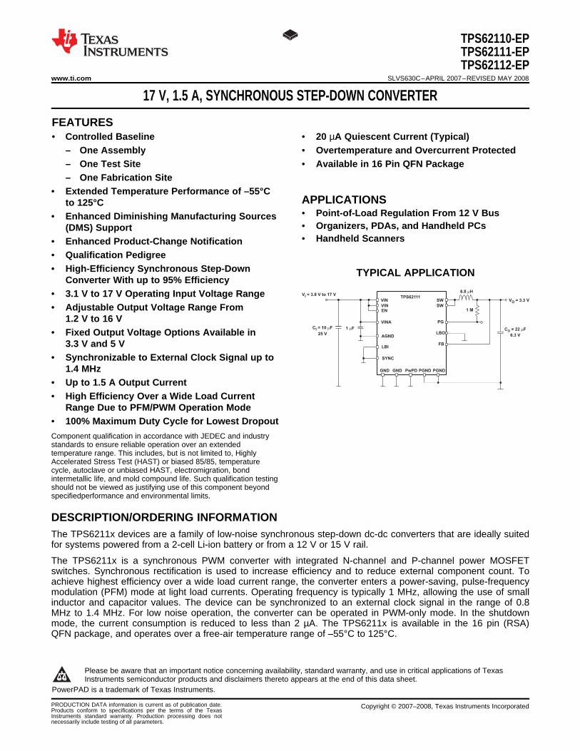
TYPICAL APPLICATION
SYNC
GND PGND
SW
VO
= 3.3 V
6.8 Hm
C = 22 F
6.3 V
Om
VIN
LBI
C = 10 F
25 V
Im 1 Fm
V = 3.8 V to 17 VI
VIN
EN
VINA
PGNDGND PwPD
AGND
TPS62111SW
LBO
PG
1 M
FB
DESCRIPTION/ORDERING INFORMATION
TPS62110-EPTPS62111-EPTPS62112-EP
www.ti.com .............................................................................................................................................................. SLVS630C–APRIL 2007–REVISED MAY 2008
17 V, 1.5 A, SYNCHRONOUS STEP-DOWN CONVERTER
2• Controlled Baseline • 20 µA Quiescent Current (Typical)– One Assembly • Overtemperature and Overcurrent Protected– One Test Site • Available in 16 Pin QFN Package– One Fabrication Site
• Extended Temperature Performance of –55°Cto 125°C
• Point-of-Load Regulation From 12 V Bus• Enhanced Diminishing Manufacturing Sources• Organizers, PDAs, and Handheld PCs(DMS) Support• Handheld Scanners• Enhanced Product-Change Notification
• Qualification Pedigree• High-Efficiency Synchronous Step-Down
Converter With up to 95% Efficiency• 3.1 V to 17 V Operating Input Voltage Range• Adjustable Output Voltage Range From
1.2 V to 16 V• Fixed Output Voltage Options Available in
3.3 V and 5 V• Synchronizable to External Clock Signal up to
1.4 MHz• Up to 1.5 A Output Current• High Efficiency Over a Wide Load Current
Range Due to PFM/PWM Operation Mode• 100% Maximum Duty Cycle for Lowest DropoutComponent qualification in accordance with JEDEC and industrystandards to ensure reliable operation over an extendedtemperature range. This includes, but is not limited to, HighlyAccelerated Stress Test (HAST) or biased 85/85, temperaturecycle, autoclave or unbiased HAST, electromigration, bondintermetallic life, and mold compound life. Such qualification testingshould not be viewed as justifying use of this component beyondspecifiedperformance and environmental limits.
The TPS6211x devices are a family of low-noise synchronous step-down dc-dc converters that are ideally suitedfor systems powered from a 2-cell Li-ion battery or from a 12 V or 15 V rail.
The TPS6211x is a synchronous PWM converter with integrated N-channel and P-channel power MOSFETswitches. Synchronous rectification is used to increase efficiency and to reduce external component count. Toachieve highest efficiency over a wide load current range, the converter enters a power-saving, pulse-frequencymodulation (PFM) mode at light load currents. Operating frequency is typically 1 MHz, allowing the use of smallinductor and capacitor values. The device can be synchronized to an external clock signal in the range of 0.8MHz to 1.4 MHz. For low noise operation, the converter can be operated in PWM-only mode. In the shutdownmode, the current consumption is reduced to less than 2 µA. The TPS6211x is available in the 16 pin (RSA)QFN package, and operates over a free-air temperature range of –55°C to 125°C.
1
Please be aware that an important notice concerning availability, standard warranty, and use in critical applications of TexasInstruments semiconductor products and disclaimers thereto appears at the end of this data sheet.
2PowerPAD is a trademark of Texas Instruments.
PRODUCTION DATA information is current as of publication date. Copyright © 2007–2008, Texas Instruments IncorporatedProducts conform to specifications per the terms of the TexasInstruments standard warranty. Production processing does notnecessarily include testing of all parameters.
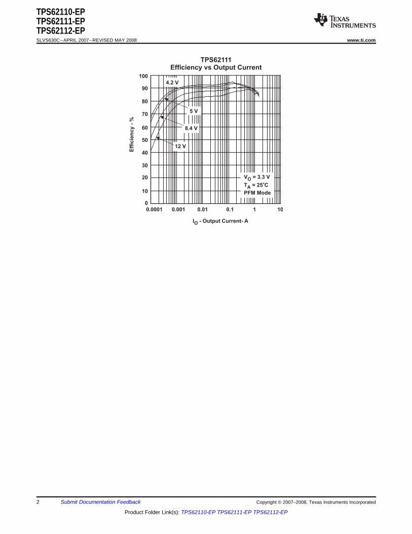
TPS62111Efficiency vs Output Current
100
0
90
70
40
20
80
50
60
30
10
0.0001 0.001 0.01 0.1 101
I - Output Current- AO
Eff
icie
ncy -
%
5 V
4.2 V
12 V
8.4 V
V = 3.3 V
T
PFM Mode
O
A = 25 Co
TPS62110-EPTPS62111-EPTPS62112-EPSLVS630C–APRIL 2007–REVISED MAY 2008 .............................................................................................................................................................. www.ti.com
2 Submit Documentation Feedback Copyright © 2007–2008, Texas Instruments Incorporated
Product Folder Link(s): TPS62110-EP TPS62111-EP TPS62112-EP
ABSOLUTE MAXIMUM RATINGS (1)
DISSIPATION RATINGS (1)
RECOMMENDED OPERATING CONDITIONS
TPS62110-EPTPS62111-EPTPS62112-EP
www.ti.com .............................................................................................................................................................. SLVS630C–APRIL 2007–REVISED MAY 2008
This device contains circuits to protect its inputs and outputs against damage due to high static voltages or electrostatic fields.These circuits have been qualified to protect this device against electrostatic discharges; HBM according to EIA/JESD22-A114-B,MM according EIA/JESD22-A115-A, and CDM according EIA/JESD22C101C; however, it is advised that precautions be taken toavoid application of any voltage higher than maximum-rated voltages to these high-impedance circuits. During storage or handlingthe device leads should be shorted together or the device should be placed in conductive foam. In a circuit, unused inputs shouldalways be connected to an appropriate logic voltage level, preferably either VCC or ground. Specific guidelines for handling devicesof this type are contained in the publication Guidelines for Handling Electrostatic-Discharge-Sensitive (ESDS) Devices andAssemblies available from Texas Instruments.
ORDERING INFORMATION (1)
TA PLASTIC QFN OUTPUT LBI/LBO MARKING16 PIN (RSA) (2) (3) VOLTAGE FUNCTIONALITYTPS62110MRSAREP Adjustable Standard TPS62110-EP
1.2 V to 16 V–55°C to 125°C TPS62111MRSAREP 3.3 V Standard TPS62111-EP
TPS62112MRSAREP 5 V Standard TPS62112-EP
(1) For the most current package and ordering information, see the Package Option Addendum at the endof this document, or see the TI website at www.ti.com.
(2) Package drawings, thermal data, and symbolization are available at www.ti.com/packaging.(3) The RSA package is available in tape and reel. Add R suffix (TPS62110RSAR) to order quantities of
3000 parts per reel. Add T suffix (TPS62110RSAT) to order quantities of 250 parts per reel
over operating free-air temperature range (unless otherwise noted)
UNITVCC Supply voltage at VIN, VINA –0.3 V to 20 V
Voltage at SW –0.3 V to VI
VI Voltage at EN, SYNC, LBO, PG –0.3 V to 20 VVoltage at LBI, FB –0.3 V to 7 V
IO Output current at SW 2400 mATJ Maximum junction temperature 150°CTstg Storage temperature –65°C to 150°C
Lead temperature 1,6 mm (1/16-inch) from case for 10 seconds 300°C
(1) Stresses beyond those listed under absolute maximum ratings may cause permanent damage to the device. These are stress ratingsonly and functional operation of the device at these or any other conditions beyond those indicated under recommended operatingconditions is not implied. Exposure to absolute-maximum-rated conditions for extended periods may affect device reliability.
TA ≤ 25°C DERATING FACTOR TA = 70°C TA = 85°CPACKAGE POWER RATING ABOVE TA = 25°C POWER RATING POWER RATINGRSA 2.5 W 25 mW/°C 1.375 W 1 W
(1) Based on a thermal resistance of 40 K/W soldered onto a high K board.
MIN MAX UNITVCC Supply voltage at VIN, VINA 3.1 17 V
Maximum voltage at power-good, LBO, EN, SYNC 17 VTJ Operating junction temperature –55 125 °C
Copyright © 2007–2008, Texas Instruments Incorporated Submit Documentation Feedback 3
Product Folder Link(s): TPS62110-EP TPS62111-EP TPS62112-EP
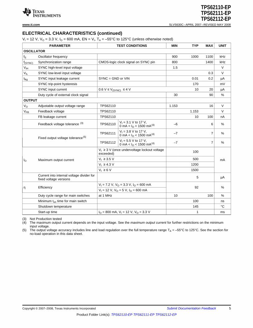
ELECTRICAL CHARACTERISTICS
TPS62110-EPTPS62111-EPTPS62112-EPSLVS630C–APRIL 2007–REVISED MAY 2008 .............................................................................................................................................................. www.ti.com
VI = 12 V, VO = 3.3 V, IO = 600 mA, EN = VI, TA = –55°C to 125°C (unless otherwise noted)
PARAMETER TEST CONDITIONS MIN TYP MAX UNITSUPPLY CURRENTVI Input voltage range (1) 3.1 17 V
IO = 0 mA, SYNC = GND, VI = 7.2 V, 20TA = 25°C (2)
I(Q) Operating quiescent current µAIO = 0 mA, SYNC = GND, 23 29VI = 17 V (2)
EN = GND 1.5 5I(SD) Shutdown current µA
EN = GND, TA = 25°C, VI = 7.2 V 1.5 3ENABLEVIH EN high-level input voltage 1.3 VVIL EN low-level input voltage 0.3 V
EN trip-point hysteresis 170 mVIIKG EN input leakage current EN = GND or VI, VI = 17 V 0.01 0.2 µAI(EN) EN input current 0.6 V ≤ V(EN) ≤ 4 V 10 µAV(UVLO) Undervoltage lockout threshold Input voltage falling 2.8 3 3.1 V
Undervoltage lockout hysteresis 250 mVPOWER SWITCH
VI ≥ 5.4 V, IO = 350 mA 165 250rDS(ON) P-channel MOSFET on-resistance VI = 3.5 V, IO = 200 mA 340 mΩ
VI = 3 V, IO = 100 mA 490P-channel MOSFET leakage VDS = 17 V 0.1 1 µAcurrentP-channel MOSFET current limit VI = 7.2 V, VO = 3.3 V 2400 mA
VI ≥ 5.4 V, IO = 350 mA 145 200rDS(ON) N-channel MOSFET on-resistance VI = 3.5 V, IO = 200 mA 170 mΩ
VI = 3 V, IO = 100 mA 200N-channel MOSFET leakage VDS = 17 V 0.1 3 µAcurrent
POWER GOOD OUTPUT, LBI, LBOV(PG) Power good trip voltage VO – 1.6% V
VO ramping positive 50Power good delay time µs
VO ramping negative 200VOL PG, LBO output low voltage V(FB) = 1.1 × VO nominal, IOL = 1 mA 0.3 VIOL PG, LBO sink current 1 mA
PG, LBO output leakage current V(FB) = VO nominal 0.01 0.25 µAMinimum supply voltage for valid 3 Vpower good, LBI, LBO signal
VLBI Low battery input trip voltage Input voltage falling 1.256 VILBI LBI input leakage current 10 100 nA
Low battery input trip-point 1.5 %accuracyVLBI,HYS Low battery input hysteresis 25 mV
(1) Not Production tested(2) Device is not switching.
4 Submit Documentation Feedback Copyright © 2007–2008, Texas Instruments Incorporated
Product Folder Link(s): TPS62110-EP TPS62111-EP TPS62112-EP
TPS62110-EPTPS62111-EPTPS62112-EP
www.ti.com .............................................................................................................................................................. SLVS630C–APRIL 2007–REVISED MAY 2008
ELECTRICAL CHARACTERISTICS (continued)VI = 12 V, VO = 3.3 V, IO = 600 mA, EN = VI, TA = –55°C to 125°C (unless otherwise noted)
PARAMETER TEST CONDITIONS MIN TYP MAX UNITOSCILLATORfS Oscillator frequency 900 1000 1100 kHzf(SYNC) Synchronization range CMOS-logic clock signal on SYNC pin 800 1400 kHzVIH SYNC high-level input voltage 1.5 VVIL SYNC low-level input voltage 0.3 VIlkg SYNC input leakage current SYNC = GND or VIN 0.01 0.2 µA
SYNC trip-point hysteresis 170 mVSYNC input current 0.6 V ≤ V(SYNC) ≤ 4 V 10 20 µADuty cycle of external clock signal 30 90 %
OUTPUTVO Adjustable output voltage range TPS62110 1.153 16 VVFB Feedback voltage TPS62110 1.153 V
FB leakage current TPS62110 10 100 nAVI = 3.1 V to 17 V,Feedback voltage tolerance (3) TPS62110 –6 6 %0 mA < IO < 1500 mA (4)
VI = 3.8 V to 17 V,TPS62111 –7 7 %0 mA < IO < 1500 mA (4)Fixed output voltage tolerance (5)
VI = 5.5 V to 17 V,TPS62112 –7 7 %0 mA < IO < 1500 mA (4)
VI ≥ 3 V (once undervoltage lockout voltage 100exceeded)VI ≥ 3.5 V 500IO Maximum output current mAVI ≥ 4.3 V 1200VI ≥ 6 V 1500
Current into internal voltage divider for 5 µAfixed voltage versionsVI = 7.2 V, VO = 3.3 V, IO = 600 mA
η Efficiency 92 %VI = 12 V, VO = 5 V, IO = 600 mA
Duty cycle range for main switches at 1 MHz 10 100 %Minimum ton time for main switch 100 nsShutdown temperature 145 °CStart-up time IO = 800 mA, VI = 12 V, VO = 3.3 V 1 ms
(3) Not Production tested(4) The maximum output current depends on the input voltage. See the maximum output current for further restrictions on the minimum
input voltage.(5) The output voltage accuracy includes line and load regulation over the full temperature range TA = –55°C to 125°C. See the section for
no-load operation in this data sheet.
Copyright © 2007–2008, Texas Instruments Incorporated Submit Documentation Feedback 5
Product Folder Link(s): TPS62110-EP TPS62111-EP TPS62112-EP
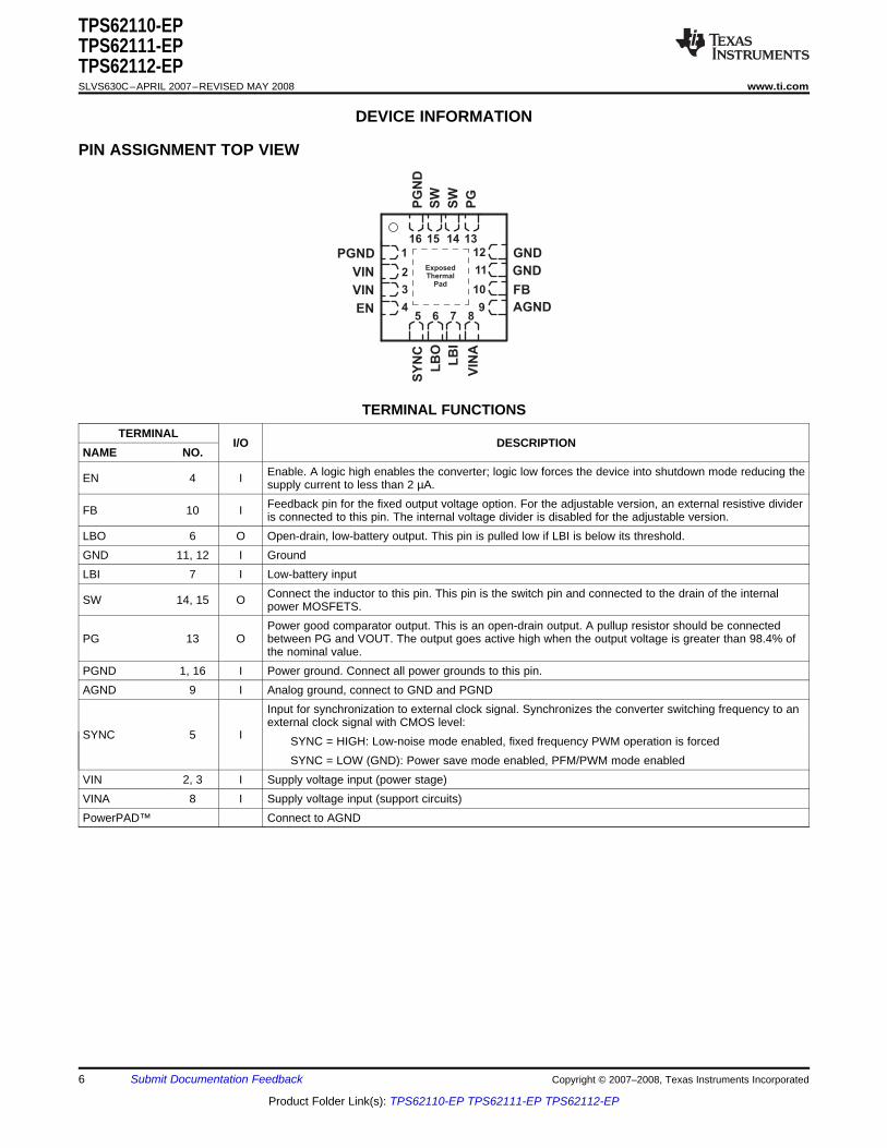
DEVICE INFORMATION
PIN ASSIGNMENT TOP VIEW
16 15 14 13
5 6 7 8
1
2
3
4 9
GND
GND
FB
AGND
PGNDExposedThermal
Pad
VIN
VIN
EN
PG
ND
SW
LB
I
VIN
A
SW
PG
SY
NC
LB
O
12
11
10
TPS62110-EPTPS62111-EPTPS62112-EPSLVS630C–APRIL 2007–REVISED MAY 2008 .............................................................................................................................................................. www.ti.com
TERMINAL FUNCTIONSTERMINAL
I/O DESCRIPTIONNAME NO.
Enable. A logic high enables the converter; logic low forces the device into shutdown mode reducing theEN 4 I supply current to less than 2 µA.Feedback pin for the fixed output voltage option. For the adjustable version, an external resistive dividerFB 10 I is connected to this pin. The internal voltage divider is disabled for the adjustable version.
LBO 6 O Open-drain, low-battery output. This pin is pulled low if LBI is below its threshold.GND 11, 12 I GroundLBI 7 I Low-battery input
Connect the inductor to this pin. This pin is the switch pin and connected to the drain of the internalSW 14, 15 O power MOSFETS.Power good comparator output. This is an open-drain output. A pullup resistor should be connected
PG 13 O between PG and VOUT. The output goes active high when the output voltage is greater than 98.4% ofthe nominal value.
PGND 1, 16 I Power ground. Connect all power grounds to this pin.AGND 9 I Analog ground, connect to GND and PGND
Input for synchronization to external clock signal. Synchronizes the converter switching frequency to anexternal clock signal with CMOS level:
SYNC 5 I SYNC = HIGH: Low-noise mode enabled, fixed frequency PWM operation is forcedSYNC = LOW (GND): Power save mode enabled, PFM/PWM mode enabled
VIN 2, 3 I Supply voltage input (power stage)VINA 8 I Supply voltage input (support circuits)PowerPAD™ Connect to AGND
6 Submit Documentation Feedback Copyright © 2007–2008, Texas Instruments Incorporated
Product Folder Link(s): TPS62110-EP TPS62111-EP TPS62112-EP
_
+
_+
_
+
_
+
_
+
REF
REF
Load Comparator
IAVG Comparator
Current Limit Comparator
P-Channel
Power MOSFET
Driver
Shoot-Through
LogicControl
Logic
Soft Start
1-MHz
Oscillator
ComparatorS
R
N-Channel
Power MOSFETComparator HighComparator Low
Comparator High 2
V(COMP)
Sawtooth
Generator
V
I
Undervoltage
Lockout
Bias Supply
_
+
Comparator High
Comparator Low
Compensation
V = 1.153 VREF
R2
(See Note A)
R1
VI
EN
SW
FB PGND
Gm
Thermal
Shutdown
Vina
_
+
_+SKIP Comparator
_
+
_+
PG
LBO
LBI GND
1.256 V
TPS62110-EPTPS62111-EPTPS62112-EP
www.ti.com .............................................................................................................................................................. SLVS630C–APRIL 2007–REVISED MAY 2008
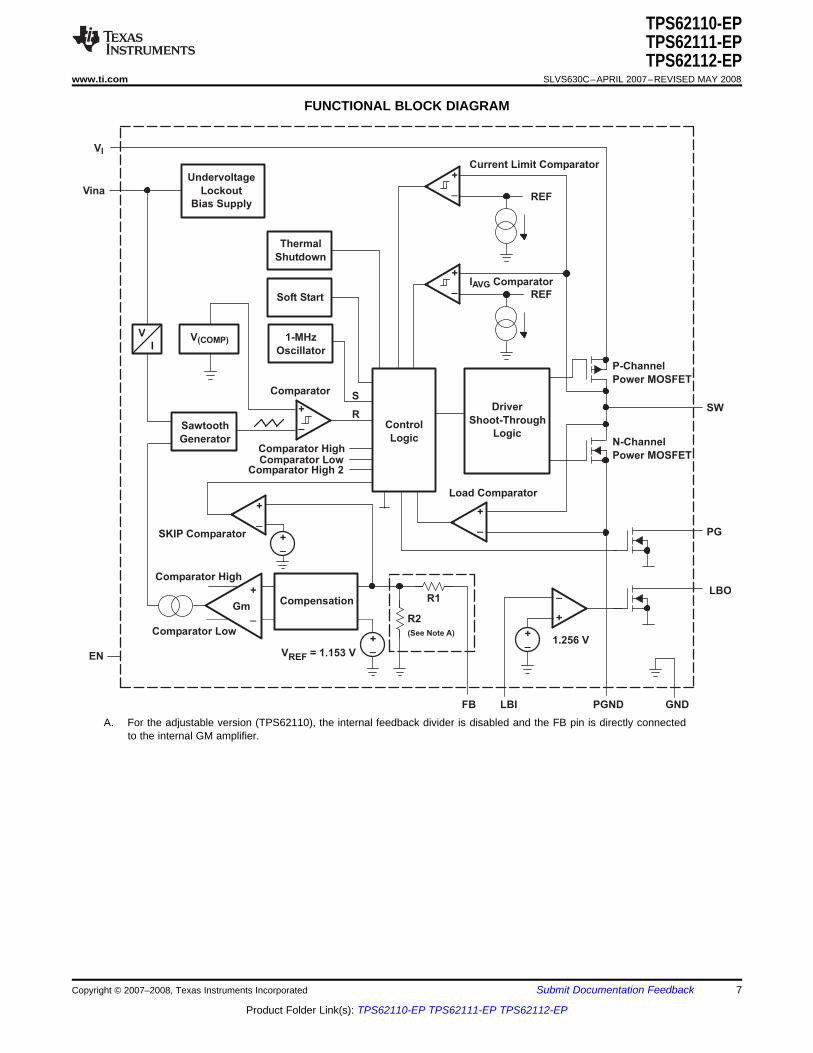
FUNCTIONAL BLOCK DIAGRAM
A. For the adjustable version (TPS62110), the internal feedback divider is disabled and the FB pin is directly connectedto the internal GM amplifier.
Copyright © 2007–2008, Texas Instruments Incorporated Submit Documentation Feedback 7
Product Folder Link(s): TPS62110-EP TPS62111-EP TPS62112-EP
TYPICAL CHARACTERISTICS
100
0
90
70
40
20
80
50
60
30
10
0.0001 0.001 0.01 0.1 101
I - Output Current- AO
Eff
icie
ncy -
%
15 V
12 V
8.4 V
V = 5 V
T
PWM Mode
O
A = 25 Co
100
0
90
70
40
20
80
50
60
30
10
0.0001 0.001 0.01 0.1 101
I - Output Current- AO
Eff
icie
ncy -
%
15 V
12 V
8.4 V
V = 5 V
T
PFM Mode
O
A = 25 Co
TPS62110-EPTPS62111-EPTPS62112-EPSLVS630C–APRIL 2007–REVISED MAY 2008 .............................................................................................................................................................. www.ti.com
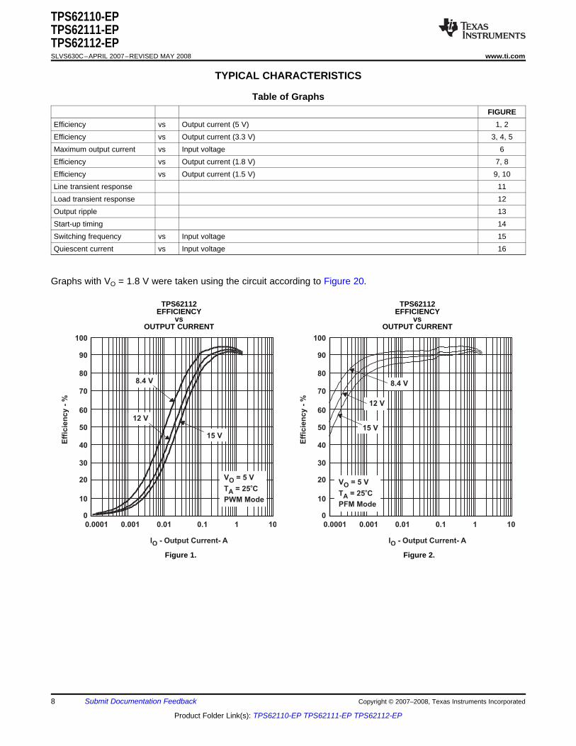
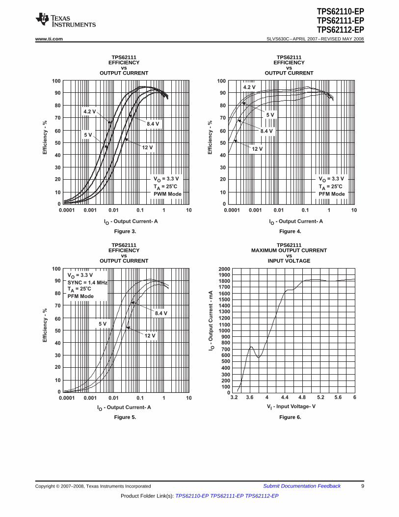
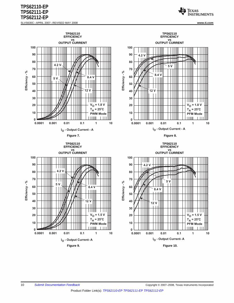
Table of GraphsFIGURE
Efficiency vs Output current (5 V) 1, 2Efficiency vs Output current (3.3 V) 3, 4, 5Maximum output current vs Input voltage 6Efficiency vs Output current (1.8 V) 7, 8Efficiency vs Output current (1.5 V) 9, 10Line transient response 11Load transient response 12Output ripple 13Start-up timing 14Switching frequency vs Input voltage 15Quiescent current vs Input voltage 16
Graphs with VO = 1.8 V were taken using the circuit according to Figure 20.
TPS62112 TPS62112EFFICIENCY EFFICIENCY
vs vsOUTPUT CURRENT OUTPUT CURRENT
Figure 1. Figure 2.
8 Submit Documentation Feedback Copyright © 2007–2008, Texas Instruments Incorporated
Product Folder Link(s): TPS62110-EP TPS62111-EP TPS62112-EP
100
0
90
70
40
20
80
50
60
30
10
0.0001 0.001 0.01 0.1 101
I - Output Current- AO
Eff
icie
ncy -
%
5 V
4.2 V
12 V
8.4 V
V = 3.3 V
T
PWM Mode
O
A = 25 Co
100
0
90
70
40
20
80
50
60
30
10
0.0001 0.001 0.01 0.1 101
I - Output Current- AO
Eff
icie
ncy -
%
5 V
4.2 V
12 V
8.4 V
V = 3.3 V
T
PFM Mode
O
A = 25 Co
2000
1600
1100
1800
1400
900
700
400
100
1900
1500
1000
1700
1200
1300
800
500
200
600
300
03.2 3.6 5.24 5.6 64.4 4.8
V - Input Voltage- VI
I-
Ou
tpu
t C
urr
en
t -
mA
O
100
0
90
70
40
20
80
50
60
30
10
0.0001 0.001 0.01 0.1 101
I - Output Current- AO
Eff
icie
ncy
- %
5 V
12 V
8.4 V
V = 3.3 V
SYNC = 1.4 MHzT
PFM Mode
O
A = 25 Co
TPS62110-EPTPS62111-EPTPS62112-EP
www.ti.com .............................................................................................................................................................. SLVS630C–APRIL 2007–REVISED MAY 2008
TPS62111 TPS62111EFFICIENCY EFFICIENCY
vs vsOUTPUT CURRENT OUTPUT CURRENT
Figure 3. Figure 4.
TPS62111 TPS62111EFFICIENCY MAXIMUM OUTPUT CURRENT
vs vsOUTPUT CURRENT INPUT VOLTAGE
Figure 5. Figure 6.
Copyright © 2007–2008, Texas Instruments Incorporated Submit Documentation Feedback 9
Product Folder Link(s): TPS62110-EP TPS62111-EP TPS62112-EP
100
0
90
70
40
20
80
50
60
30
10
0.0001 0.001 0.01 0.1 101
I - Output Current - AO
Eff
icie
ncy -
%
5 V
4.2 V
12 V
8.4 V
V = 1.8 V
T
PFM Mode
O
A = 25 Co
100
0
90
70
40
20
80
50
60
30
10
0.0001 0.001 0.01 0.1 101
I - Output Current - AO
Eff
icie
ncy -
%
5 V
4.2 V
12 V
8.4 V
V = 1.8 V
T
PWM Mode
O
A = 25 Co
100
0
90
70
40
20
80
50
60
30
10
0.0001 0.001 0.01 0.1 101
I - Output Current- AO
Eff
icie
ncy -
%
5 V
4.2 V
12 V
8.4 V
V = 1.5 V
T
PFM Mode
O
A = 25 Co
100
0
90
70
40
20
80
50
60
30
10
0.0001 0.001 0.01 0.1 101
I - Output Current- AO
Eff
icie
ncy -
% 5 V
4.2 V
12 V
8.4 V
V = 1.5 V
T
PWM Mode
O
A = 25 Co
TPS62110-EPTPS62111-EPTPS62112-EPSLVS630C–APRIL 2007–REVISED MAY 2008 .............................................................................................................................................................. www.ti.com
TPS62110 TPS62110EFFICIENCY EFFICIENCY
vs vsOUTPUT CURRENT OUTPUT CURRENT
Figure 7. Figure 8.
TPS62110 TPS62110EFFICIENCY EFFICIENCY
vs vsOUTPUT CURRENT OUTPUT CURRENT
Figure 9. Figure 10.
10 Submit Documentation Feedback Copyright © 2007–2008, Texas Instruments Incorporated
Product Folder Link(s): TPS62110-EP TPS62111-EP TPS62112-EP
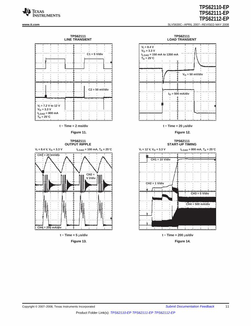
t − Time = 2 ms/div
VI = 7.2 V to 12 VVO = 3.3 VILOAD = 800 mATA = 25°C
C2 = 50 mV/div
C1 = 5 V/div
t − Time = 20 µs/div
VI = 8.4 VVO = 3.3 VILOAD = 150 mA to 1350 mATA = 25°C
VO = 50 mV/div
IO = 500 mA/div
t − Time = 5 µs/div
CH1 = 20 mV/div
VI = 8.4 V, VO = 3.3 V
CH2 =5 V/div
CH4 = 200 mA/div
ILOAD = 100 mA, TA = 25°C
t − Time = 200 µs/div
CH1 = 10 V/div
VI = 12 V, VO = 3.3 V
CH4 = 500 mA/div
ILOAD = 800 mA, TA = 25°C
CH3 = 5 V/div
CH2 = 1 V/div
TPS62110-EPTPS62111-EPTPS62112-EP
www.ti.com .............................................................................................................................................................. SLVS630C–APRIL 2007–REVISED MAY 2008
TPS62111 TPS62111LINE TRANSIENT LOAD TRANSIENT
Figure 11. Figure 12.
TPS62111 TPS62111OUTPUT RIPPLE START-UP TIMING
Figure 13. Figure 14.
Copyright © 2007–2008, Texas Instruments Incorporated Submit Documentation Feedback 11
Product Folder Link(s): TPS62110-EP TPS62111-EP TPS62112-EP
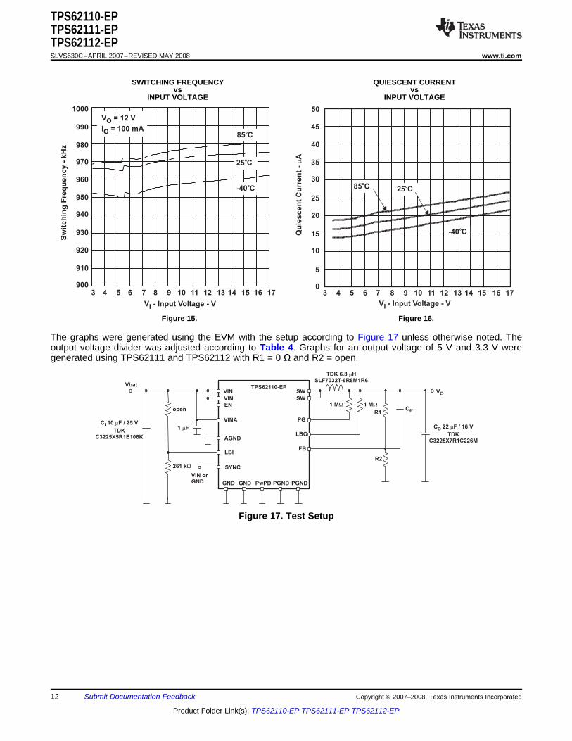
1000
970
930
940
900
980
950
910
990
960
920
3 75 94 86 10 1412 1611 1513 17
V - Input Voltage - VI
Sw
itc
hin
g F
req
ue
nc
y -
kH
z
25 Co
-40 Co
85 Co
V = 12 V
IO
O = 100 mA
0
10
30
20
40
5
15
35
25
45
50
3 75 94 86 10 1412 1611 1513 17
V - Input Voltage - VIQ
uie
scen
t C
urr
en
t -
Am
25 Co
-40 Co
85 Co
SYNC
GND PGND
SW
R1
R2
VO
TDK 6.8 HSLF7032T-6R8M1R6
m
C 22 F / 16 V
TDKO m
C3225X7R1C226M
VIN
LBI
C 10 F / 25 V
TDKI m
C3225X5R1E106K
1 Fm
261 kW
Vbat
VINEN
VINA
PGNDGND PwPD
open
VIN orGND
AGND
TPS62110SW
LBO
PG
1 MW 1 MW
FB
Cff
-EP
TPS62110-EPTPS62111-EPTPS62112-EPSLVS630C–APRIL 2007–REVISED MAY 2008 .............................................................................................................................................................. www.ti.com
SWITCHING FREQUENCY QUIESCENT CURRENTvs vs
INPUT VOLTAGE INPUT VOLTAGE
Figure 15. Figure 16.
The graphs were generated using the EVM with the setup according to Figure 17 unless otherwise noted. Theoutput voltage divider was adjusted according to Table 4. Graphs for an output voltage of 5 V and 3.3 V weregenerated using TPS62111 and TPS62112 with R1 = 0 Ω and R2 = open.
Figure 17. Test Setup
12 Submit Documentation Feedback Copyright © 2007–2008, Texas Instruments Incorporated
Product Folder Link(s): TPS62110-EP TPS62111-EP TPS62112-EP
DETAILED DESCRIPTION
OPERATION
CONSTANT FREQUENCY MODE OPERATION (SYNC = HIGH)
POWER SAVE MODE OPERATION (SYNC = LOW)
TPS62110-EPTPS62111-EPTPS62112-EP
www.ti.com .............................................................................................................................................................. SLVS630C–APRIL 2007–REVISED MAY 2008
The TPS6211x is a synchronous step-down converter that operates with a 1 MHz fixed frequency pulse widthmodulation (PWM) at moderate-to-heavy load currents and enters the power save mode at light load current.
During PWM operation, the converter uses a unique fast response voltage mode control scheme with inputvoltage feedforward. Good line and load regulation is achieved with the use of small input and output ceramiccapacitors. At the beginning of each clock cycle initiated by the clock signal (S), the P-channel MOSFET switchis turned on, and the inductor current ramps up until the comparator trips and the control logic turns the switchoff. The switch is turned off by the current limit comparator if the current limit of the P-channel switch isexceeded. After the dead time prevents current shoot through, the N-channel MOSFET rectifier is turned on, andthe inductor current ramps down. The next cycle is initiated by the clock signal turning off the N-channel rectifier,and turning on the P-channel switch.
The error amplifier as well as the input voltage determines the rise time of the sawtooth generator. Therefore,any change in input voltage or output voltage directly controls the duty cycle of the converter giving a very goodline and load transient regulation.
In constant frequency mode, the output voltage is regulated by varying the duty cycle of the PWM signal in therange of 100% to 10%. Connecting the SYNC pin to a voltage greater than 1.5 V forces the converter to operatepermanently in the PWM mode even at light or no-load currents. The advantage is that the converter operateswith a fixed switching frequency that allows simple filtering of the switching frequency for noise-sensitiveapplications. In this mode, the efficiency is lower compared to the power save mode during light loads. TheN-MOSFET of the devices stay on even when the current into the output drops to zero. This prevents the devicefrom going into discontinuous mode, and the device transfers unused energy back to the input. Therefore, thereis no ringing at the output, which usually occurs in discontinuous mode. The duty cycle range in constantfrequency mode is 100% to 10%.
It is possible to switch from forced PWM mode to the power save mode during operation by pulling the SYNC pinLOW. The flexible configuration of the SYNC pin during operation of the device allows efficient powermanagement by adjusting the operation of the TPS6211x to the specific system requirements.
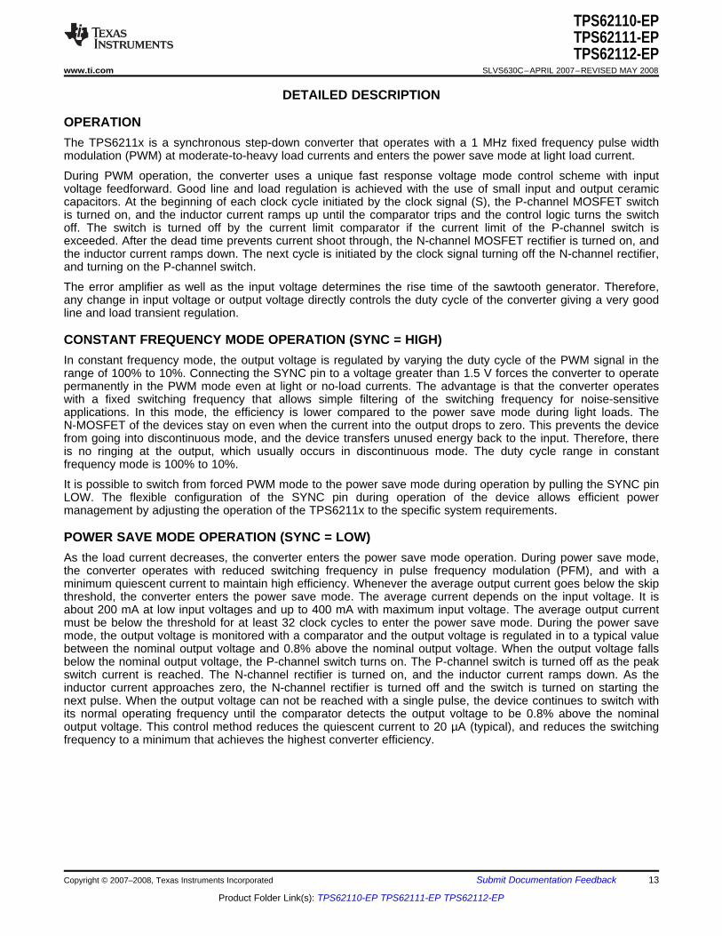
As the load current decreases, the converter enters the power save mode operation. During power save mode,the converter operates with reduced switching frequency in pulse frequency modulation (PFM), and with aminimum quiescent current to maintain high efficiency. Whenever the average output current goes below the skipthreshold, the converter enters the power save mode. The average current depends on the input voltage. It isabout 200 mA at low input voltages and up to 400 mA with maximum input voltage. The average output currentmust be below the threshold for at least 32 clock cycles to enter the power save mode. During the power savemode, the output voltage is monitored with a comparator and the output voltage is regulated in to a typical valuebetween the nominal output voltage and 0.8% above the nominal output voltage. When the output voltage fallsbelow the nominal output voltage, the P-channel switch turns on. The P-channel switch is turned off as the peakswitch current is reached. The N-channel rectifier is turned on, and the inductor current ramps down. As theinductor current approaches zero, the N-channel rectifier is turned off and the switch is turned on starting thenext pulse. When the output voltage can not be reached with a single pulse, the device continues to switch withits normal operating frequency until the comparator detects the output voltage to be 0.8% above the nominaloutput voltage. This control method reduces the quiescent current to 20 µA (typical), and reduces the switchingfrequency to a minimum that achieves the highest converter efficiency.
Copyright © 2007–2008, Texas Instruments Incorporated Submit Documentation Feedback 13
Product Folder Link(s): TPS62110-EP TPS62111-EP TPS62112-EP
V (nominal)O
0.8%
1.6%
-1.6%t
W»
2 5
IV
S K I PI
(1)
SOFT START
100% DUTY CYCLE LOW DROPOUT OPERATION
( ))(max)(maxmaxmin LRonDSrOIOVIV +×+=(2)
TPS62110-EPTPS62111-EPTPS62112-EPSLVS630C–APRIL 2007–REVISED MAY 2008 .............................................................................................................................................................. www.ti.com
DETAILED DESCRIPTION (continued)
Figure 18. Power Save Mode Output Voltage Thresholds
The typical PFM (SKIP) current threshold for the TPS6211x is given by:
Equation 1 is valid for input voltages up to 7 V. For higher voltages, the skip current threshold is not increasedfurther. The converter enters the fixed frequency PWM mode as soon as the output voltage falls below VO –1.6% (nominal).
The TPS6211x has an internal soft-start circuit that limits the inrush current during start-up. This preventspossible voltage drops of the input voltage when a battery or a high-impedance power source is connected to theinput of the TPS6211x.
The soft start is implemented as a digital circuit increasing the switch current in steps of 300 mA, 600 mA,1200 mA. The typical switch current limit is 2.4 A. Therefore, the start-up time depends on the output capacitorand load current. Typical start-up time with a 22 µF output capacitor and 800-mA load current is 1 ms.
The TPS6211x offers the lowest possible input to output voltage difference while still maintaining operation withthe use of the 100% duty cycle mode. In this mode, the P-channel switch is constantly turned on. This isparticularly useful in battery-powered applications to achieve the longest operation time, taking full advantage ofthe whole battery voltage range. The minimum input voltage to maintain regulation depends on the load currentand output voltage, and is calculated as:
with:IOmax = maximum output current plus inductor ripple currentrDS(on)max = maximum P-channel switch rDS(on)R(L) = dc resistance of the inductorVOmax = nominal output voltage plus maximum output voltage tolerance
14 Submit Documentation Feedback Copyright © 2007–2008, Texas Instruments Incorporated
Product Folder Link(s): TPS62110-EP TPS62111-EP TPS62112-EP
ENABLE
UNDERVOLTAGE LOCKOUT
SYNCHRONIZATION
POWER GOOD COMPARATOR
LOW-BATTERY DETECTOR
TPS62110-EPTPS62111-EPTPS62112-EP
www.ti.com .............................................................................................................................................................. SLVS630C–APRIL 2007–REVISED MAY 2008
DETAILED DESCRIPTION (continued)
Logic low on EN forces the TPS6211x into shutdown. In shutdown, the power switch, drivers, voltage reference,oscillator, and all other functions are turned off. The supply current is reduced to less than 2 µA in the shutdownmode. When the device is in thermal shutdown, the bandgap is forced to be switched on even if the device is setinto shutdown by pulling EN to GND.
If an output voltage is present when the device is disabled, which could be due to an external voltage source or asuper capacitor, the reverse leakage current is specified under electrical characteristics. Pulling the enable pinhigh starts up the TPS6211x with the soft start. If the EN pin is connected to any voltage other than VI or GND,an increased leakage current of typically 10 µA and up to 20 µA can occur.
The undervoltage lockout circuit prevents the device from misoperation at low-input voltages. It prevents theconverter from turning on the switch or rectifier MOSFET under undefined conditions. The minimum input voltageto start up the TPS6211x is 3.4 V (worst case). The device shuts down at 2.8 V minimum.
If no clock signal is applied, the converter operates with a typical switching frequency of 1 MHz. It is possible tosynchronize the converter to an external clock within a frequency range from 0.8 MHz to 1.4 MHz. The deviceautomatically detects the rising edge of the first clock and synchronizes immediately to the external clock. If theclock signal is stopped, the converter automatically switches back to the internal clock and continues operation.The switch over is initiated if no rising edge on the SYNC pin is detected for a duration of four clock cycles.Therefore, the maximum delay time can be 6.25 µs if the internal clock has its minimum frequency of 800 kHz.
If the device is synchronized to an external clock, the power save mode is disabled, and the devices stay inforced PWM mode.
Connecting the SYNC pin to the GND pin enables the power save mode. The converter operates in the PWMmode at moderate-to-heavy loads, and in the PFM mode during light loads, which maintains high efficiency overa wide load current range.
The power good (PG) comparator has an open-drain output capable of sinking 1 mA (typical). The PG is activeonly when the device is enabled (EN=high). When the device is disabled (EN=low), the PG pin is pulled to GND.
The PG output is valid only after a 250-µs delay when the device is enabled, and the supply voltage is greaterthan the undervoltage lockout V(UVLO). PG is low during the first 250 µs after shutdown and in shutdown.
The PG pin becomes active high when the output voltage exceeds 98.4% (typical) of its nominal value. Leavethe PG pin unconnected when not used.
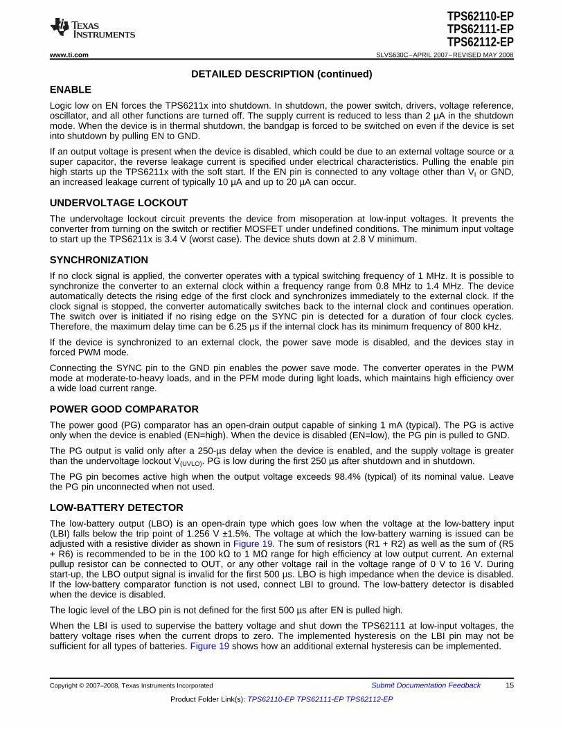
The low-battery output (LBO) is an open-drain type which goes low when the voltage at the low-battery input(LBI) falls below the trip point of 1.256 V ±1.5%. The voltage at which the low-battery warning is issued can beadjusted with a resistive divider as shown in Figure 19. The sum of resistors (R1 + R2) as well as the sum of (R5+ R6) is recommended to be in the 100 kΩ to 1 MΩ range for high efficiency at low output current. An externalpullup resistor can be connected to OUT, or any other voltage rail in the voltage range of 0 V to 16 V. Duringstart-up, the LBO output signal is invalid for the first 500 µs. LBO is high impedance when the device is disabled.If the low-battery comparator function is not used, connect LBI to ground. The low-battery detector is disabledwhen the device is disabled.
The logic level of the LBO pin is not defined for the first 500 µs after EN is pulled high.
When the LBI is used to supervise the battery voltage and shut down the TPS62111 at low-input voltages, thebattery voltage rises when the current drops to zero. The implemented hysteresis on the LBI pin may not besufficient for all types of batteries. Figure 19 shows how an additional external hysteresis can be implemented.
Copyright © 2007–2008, Texas Instruments Incorporated Submit Documentation Feedback 15
Product Folder Link(s): TPS62110-EP TPS62111-EP TPS62112-EP
SYNC
GND PGND
SW
R1560 k
R2300 k
VO = 3.3 V
6.8 Hm
C = 22 F
6.3 VO m
VIN
LBI
C = 10 F
25 VI m 1 Fm
2
3
4
8
9
7
5
11 12 16
10
6
13
14
15
1
V = 4.3 V to 17 VI
VINEN
VINA
PGNDGND PwPD
R5
R6
AGND
TPS62110SW
LBO
PG
R3
R7
R4
FB
Cff
10 pF
NO LOAD OPERATION
THEORY OR OPERATION / DESIGN PROCEDURE
Inductor Selection
TPS62110-EPTPS62111-EPTPS62112-EPSLVS630C–APRIL 2007–REVISED MAY 2008 .............................................................................................................................................................. www.ti.com
DETAILED DESCRIPTION (continued)
Figure 19. LBI With Increased Hysteresis
When the converter operates in the forced PWM mode and there is no load connected to the output, theconverter regulates the output voltage by allowing the inductor current to reverse for a short time.
Table 1. List of InductorsMANUFACTURER (1) TYPE INDUCTANCE DC RESISTANCE SATURATION CURRENT
Coilcraft MSS6132-682 6.8 µH 65 mR (max) 1.5 AEpcos B82462G4682M 6.8 µH 50 mR (max) 1.5 ASumida CDRH5D28-6R2 6.2 µH 33 mR (typ) 1.8 A
SLF6028T-6R8M1R5 6.8 µH 35 mR (typ) 1.5 ATDK
SLF7032T-6R8M1R6 6.8 µH 41 mR (typ) 1.6 A7447789006 6.8 µH 44 mR (typ) 2.75 A
Wurth 7447779006 6.8 µH 33 mR (typ) 3.3 A744053006 6.2 µH 45 mR (typ) 1.8 A
(1) The manufacturer's part numbers are used for test purposes only.
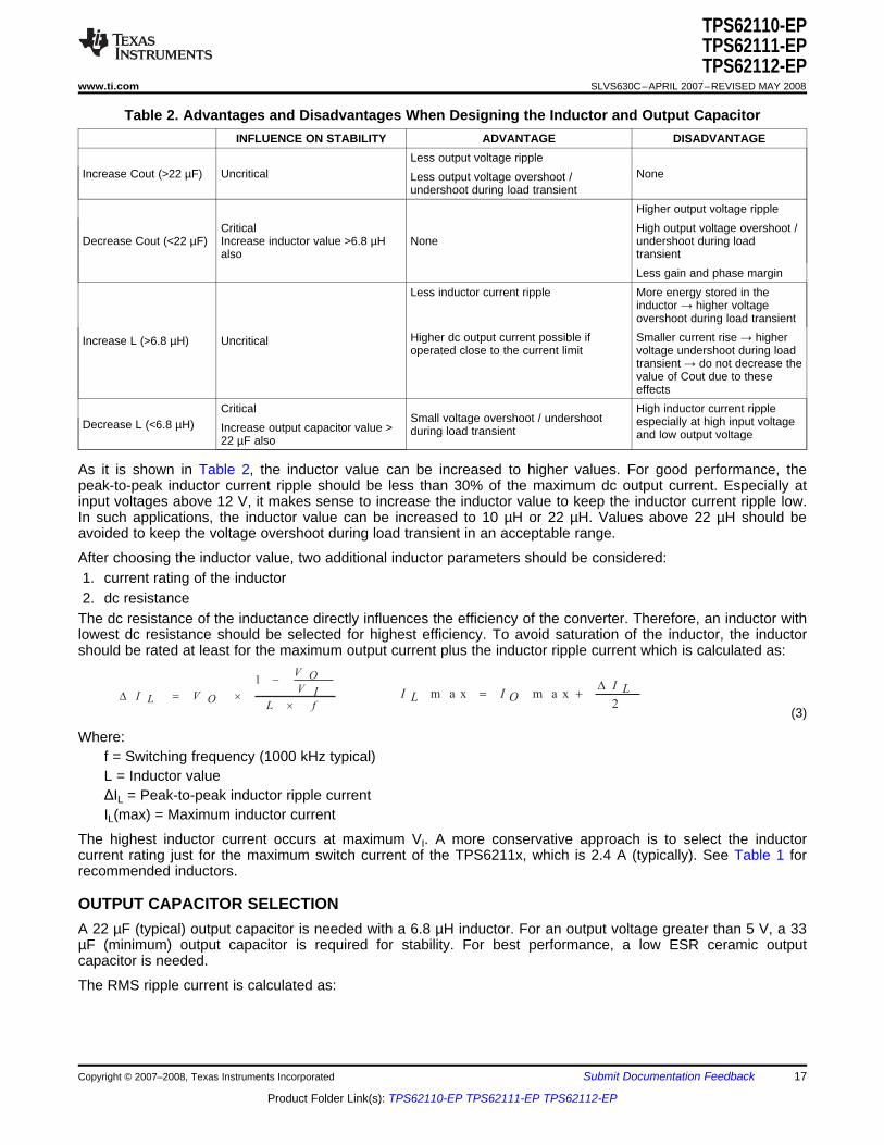
The control loop of the TPS6211x family requires a certain value for the output inductor and the output capacitorfor stable operation. As long as the nominal value of L × C ≥ 6.2 µH × 22 µF, the control loop has enough phasemargin and the device is stable. Reducing the inductor value without increasing the output capacitor (or viceversa) may cause stability problems. There are applications where it may be useful to increase the value of theoutput capacitor, e.g., for a low transient output voltage change. From a stability point of view, the inductor valuecould be decreased to keep the L × C product constant. However, there are drawbacks if the inductor value isdecreased. A low inductor value causes a high inductor ripple current and therefore reduces the maximum dcoutput current. Table 2 gives the advantages and disadvantages when designing the inductor and outputcapacitor.
16 Submit Documentation Feedback Copyright © 2007–2008, Texas Instruments Incorporated
Product Folder Link(s): TPS62110-EP TPS62111-EP TPS62112-EP
fL
IV
OV
OVLI´
-
´=D
1
2m a xm a x
LIOILI
D+=
(3)
OUTPUT CAPACITOR SELECTION
TPS62110-EPTPS62111-EPTPS62112-EP
www.ti.com .............................................................................................................................................................. SLVS630C–APRIL 2007–REVISED MAY 2008
Table 2. Advantages and Disadvantages When Designing the Inductor and Output CapacitorINFLUENCE ON STABILITY ADVANTAGE DISADVANTAGE
Less output voltage rippleIncrease Cout (>22 µF) Uncritical NoneLess output voltage overshoot /
undershoot during load transientHigher output voltage ripple
Critical High output voltage overshoot /Decrease Cout (<22 µF) Increase inductor value >6.8 µH None undershoot during load
also transientLess gain and phase margin
Less inductor current ripple More energy stored in theinductor → higher voltageovershoot during load transient
Higher dc output current possible if Smaller current rise → higherIncrease L (>6.8 µH) Uncriticaloperated close to the current limit voltage undershoot during load
transient → do not decrease thevalue of Cout due to theseeffects
Critical High inductor current rippleSmall voltage overshoot / undershoot especially at high input voltageDecrease L (<6.8 µH) Increase output capacitor value > during load transient and low output voltage22 µF also
As it is shown in Table 2, the inductor value can be increased to higher values. For good performance, thepeak-to-peak inductor current ripple should be less than 30% of the maximum dc output current. Especially atinput voltages above 12 V, it makes sense to increase the inductor value to keep the inductor current ripple low.In such applications, the inductor value can be increased to 10 µH or 22 µH. Values above 22 µH should beavoided to keep the voltage overshoot during load transient in an acceptable range.
After choosing the inductor value, two additional inductor parameters should be considered:1. current rating of the inductor2. dc resistance
The dc resistance of the inductance directly influences the efficiency of the converter. Therefore, an inductor withlowest dc resistance should be selected for highest efficiency. To avoid saturation of the inductor, the inductorshould be rated at least for the maximum output current plus the inductor ripple current which is calculated as:
Where:f = Switching frequency (1000 kHz typical)L = Inductor valueΔIL = Peak-to-peak inductor ripple currentIL(max) = Maximum inductor current
The highest inductor current occurs at maximum VI. A more conservative approach is to select the inductorcurrent rating just for the maximum switch current of the TPS6211x, which is 2.4 A (typically). See Table 1 forrecommended inductors.
A 22 µF (typical) output capacitor is needed with a 6.8 µH inductor. For an output voltage greater than 5 V, a 33µF (minimum) output capacitor is required for stability. For best performance, a low ESR ceramic outputcapacitor is needed.
The RMS ripple current is calculated as:
Copyright © 2007–2008, Texas Instruments Incorporated Submit Documentation Feedback 17
Product Folder Link(s): TPS62110-EP TPS62111-EP TPS62112-EP
32
11
)(´
´
´
-
´=
fL
IV
OV
OVOCR M SI
(4)
÷÷ø
öççè
æ+
´´´
´
-
´=D E S RRfOCfL
IV
OV
OVOV8
11
(5)
INPUT CAPACITOR SELECTION
÷÷ø
öççè
æ-´´=
IV
OV
IV
OV
OIR M SI 1m a x
(6)
FEEDFORWARD CAPACITOR SELECTION
RECOMMENDED CAPACITORS
TPS62110-EPTPS62111-EPTPS62112-EPSLVS630C–APRIL 2007–REVISED MAY 2008 .............................................................................................................................................................. www.ti.com
The overall output ripple voltage is the sum of the voltage spike caused by the output capacitor ESR plus thevoltage ripple caused by charge and discharging the output capacitor:
Where the highest output voltage ripple occurs at the highest input voltage VI.
The nature of the buck converter is a pulsating input current; therefore, a low ESR input capacitor is required forbest input voltage filtering, and minimizing the interference with other circuits caused by high input voltagespikes. The input capacitor should have a minimum value of 10 µF and can be increased without any limit forbetter input voltage filtering. The input capacitor should be rated for the maximum input ripple current calculatedas:
The worst-case RMS ripple current occurs at D = 0.5 and is calculated as: IRMS = IO/2. Ceramic capacitors showa good performance because of their low ESR value, and they are less sensitive against voltage transientscompared to tantalum capacitors. Place the input capacitor as close as possible to the input pin of the IC for bestperformance
The feedforward capacitor (Cff) is needed to compensate for parasitic capacitance from the feedback pin to GND.Typically, a value of 4.7 pF to 22 pF is needed for an output voltage divider with a equivalent resistance (R1 inparallel with R2) in the 150 kΩ range. The value can be chosen based on best transient performance and lowestoutput voltage ripple in PFM mode.
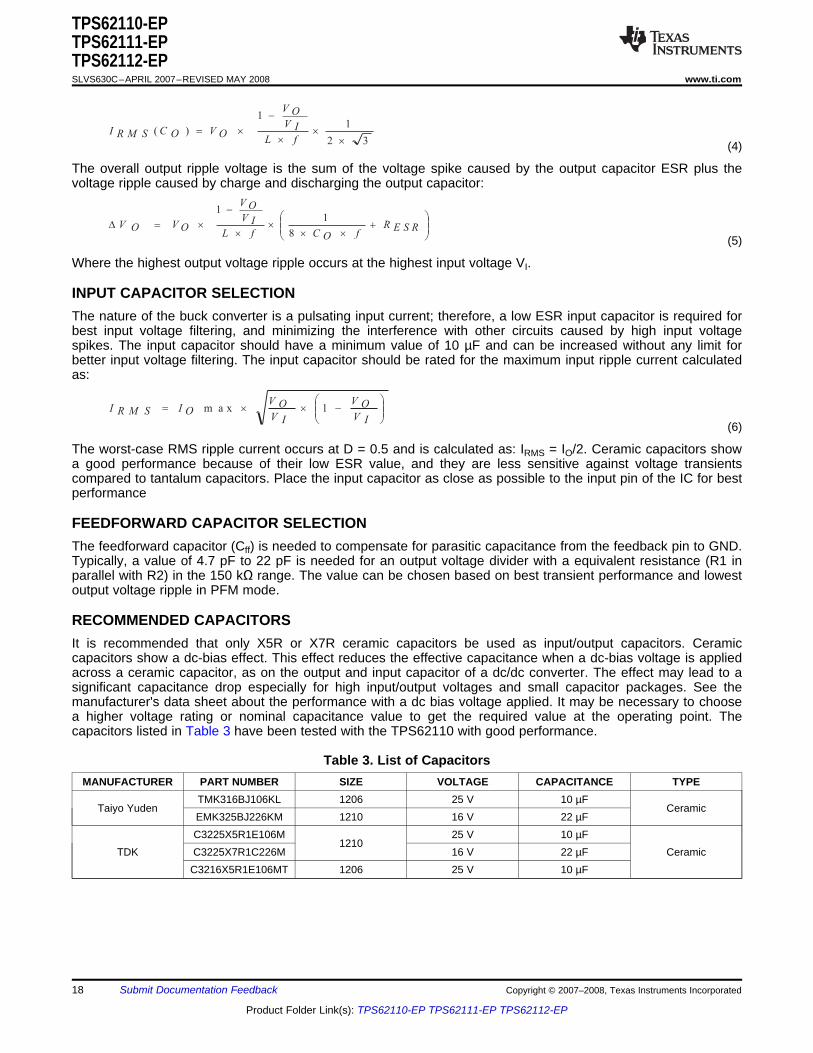
It is recommended that only X5R or X7R ceramic capacitors be used as input/output capacitors. Ceramiccapacitors show a dc-bias effect. This effect reduces the effective capacitance when a dc-bias voltage is appliedacross a ceramic capacitor, as on the output and input capacitor of a dc/dc converter. The effect may lead to asignificant capacitance drop especially for high input/output voltages and small capacitor packages. See themanufacturer's data sheet about the performance with a dc bias voltage applied. It may be necessary to choosea higher voltage rating or nominal capacitance value to get the required value at the operating point. Thecapacitors listed in Table 3 have been tested with the TPS62110 with good performance.
Table 3. List of CapacitorsMANUFACTURER PART NUMBER SIZE VOLTAGE CAPACITANCE TYPE
TMK316BJ106KL 1206 25 V 10 µFTaiyo Yuden Ceramic
EMK325BJ226KM 1210 16 V 22 µFC3225X5R1E106M 25 V 10 µF
1210TDK C3225X7R1C226M 16 V 22 µF Ceramic
C3216X5R1E106MT 1206 25 V 10 µF
18 Submit Documentation Feedback Copyright © 2007–2008, Texas Instruments Incorporated
Product Folder Link(s): TPS62110-EP TPS62111-EP TPS62112-EP
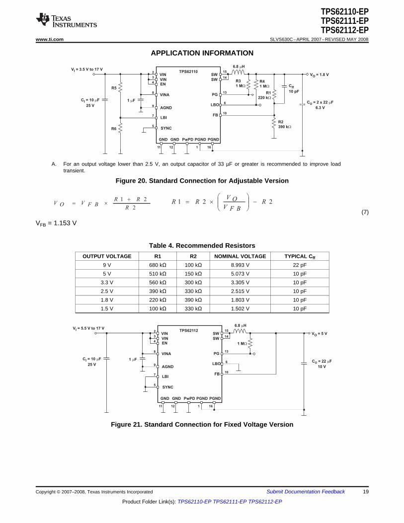
APPLICATION INFORMATION
SYNC
GND PGND
SW
R1
220 kW
R2
390 kW
VO = 1.8 V
6.8 Hm
C = 2 x 22 F
6.3 VO m
VIN
LBI
C = 10 F
25 VI m 1 Fm
2
3
4
8
9
7
5
11 12 16
10
6
13
14
15
1
V = 3.5 V to 17 VI
VINEN
VINA
PGNDGND PwPD
R5
R6
AGND
TPS62110SW
LBO
PG
R3
1 MWR4
1 MW
FB
Cff
10 pF
2
21
R
RR
F BVOV+
´= 221 R
F BV
OVRR -÷
÷ø
öççè
æ´=
(7)
SYNC
GND PGND
SW
VO
= 5 V
6.8 Hm
C = 22 F
10 V
Om
VIN
LBI
C = 10 F
25 V
Im 1 Fm
2
3
4
8
9
7
5
11 12 16
10
6
13
14
15
1
V = 5.5 V to 17 VI
VIN
EN
VINA
PGNDGND PwPD
AGND
TPS62112SW
LBO
PG
1 MW
FB
TPS62110-EPTPS62111-EPTPS62112-EP
www.ti.com .............................................................................................................................................................. SLVS630C–APRIL 2007–REVISED MAY 2008
A. For an output voltage lower than 2.5 V, an output capacitor of 33 µF or greater is recommended to improve loadtransient.
Figure 20. Standard Connection for Adjustable Version
VFB = 1.153 V
Table 4. Recommended ResistorsOUTPUT VOLTAGE R1 R2 NOMINAL VOLTAGE TYPICAL Cff
9 V 680 kΩ 100 kΩ 8.993 V 22 pF5 V 510 kΩ 150 kΩ 5.073 V 10 pF
3.3 V 560 kΩ 300 kΩ 3.305 V 10 pF2.5 V 390 kΩ 330 kΩ 2.515 V 10 pF1.8 V 220 kΩ 390 kΩ 1.803 V 10 pF1.5 V 100 kΩ 330 kΩ 1.502 V 10 pF
Figure 21. Standard Connection for Fixed Voltage Version
Copyright © 2007–2008, Texas Instruments Incorporated Submit Documentation Feedback 19
Product Folder Link(s): TPS62110-EP TPS62111-EP TPS62112-EP
SYNC
GND PGND
SW
R1
680 kW
R2
100 kW
VO = 9 V
6.8 Hm
C = 33 F
16 VO m
VIN
LBI
C = 10 F
25 VI m 1 Fm
2
3
4
8
9
7
5
11 12 16
10
6
13
14
15
1
V = 9.3 V to 17 VI
VINEN
VINA
PGNDGND PwPD
AGND
TPS62110SW
LBO
PG
1 MW
FB
Cff22 pF
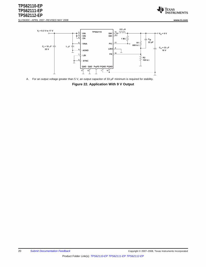
TPS62110-EPTPS62111-EPTPS62112-EPSLVS630C–APRIL 2007–REVISED MAY 2008 .............................................................................................................................................................. www.ti.com
A. For an output voltage greater than 5 V, an output capacitor of 33 µF minimum is required for stability.
Figure 22. Application With 9 V Output
20 Submit Documentation Feedback Copyright © 2007–2008, Texas Instruments Incorporated
Product Folder Link(s): TPS62110-EP TPS62111-EP TPS62112-EP
PACKAGE OPTION ADDENDUM
www.ti.com 31-May-2014
Addendum-Page 1
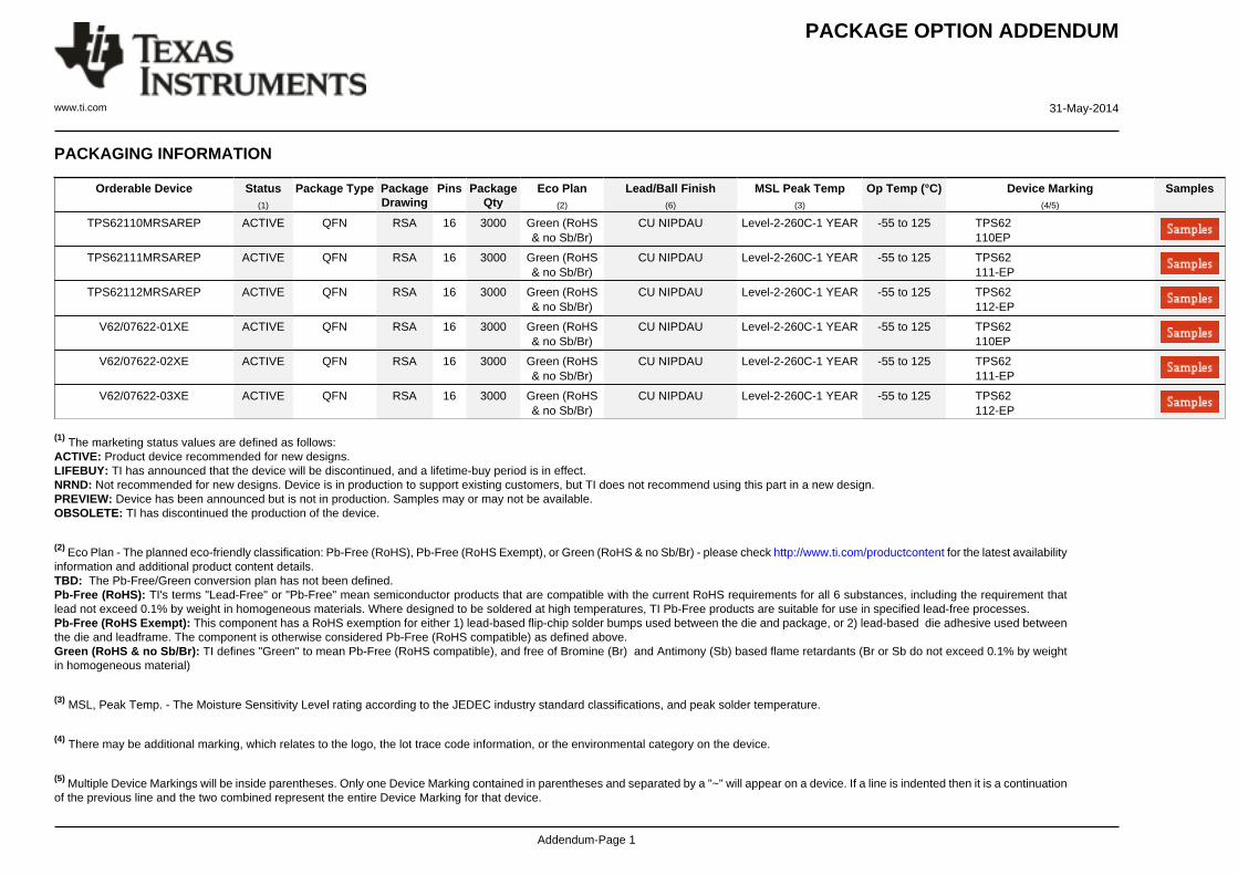
PACKAGING INFORMATION
Orderable Device Status(1)
Package Type PackageDrawing
Pins PackageQty
Eco Plan(2)
Lead/Ball Finish(6)
MSL Peak Temp(3)
Op Temp (°C) Device Marking(4/5)
Samples
TPS62110MRSAREP ACTIVE QFN RSA 16 3000 Green (RoHS& no Sb/Br)
CU NIPDAU Level-2-260C-1 YEAR -55 to 125 TPS62110EP
TPS62111MRSAREP ACTIVE QFN RSA 16 3000 Green (RoHS& no Sb/Br)
CU NIPDAU Level-2-260C-1 YEAR -55 to 125 TPS62111-EP
TPS62112MRSAREP ACTIVE QFN RSA 16 3000 Green (RoHS& no Sb/Br)
CU NIPDAU Level-2-260C-1 YEAR -55 to 125 TPS62112-EP
V62/07622-01XE ACTIVE QFN RSA 16 3000 Green (RoHS& no Sb/Br)
CU NIPDAU Level-2-260C-1 YEAR -55 to 125 TPS62110EP
V62/07622-02XE ACTIVE QFN RSA 16 3000 Green (RoHS& no Sb/Br)
CU NIPDAU Level-2-260C-1 YEAR -55 to 125 TPS62111-EP
V62/07622-03XE ACTIVE QFN RSA 16 3000 Green (RoHS& no Sb/Br)
CU NIPDAU Level-2-260C-1 YEAR -55 to 125 TPS62112-EP
(1) The marketing status values are defined as follows:ACTIVE: Product device recommended for new designs.LIFEBUY: TI has announced that the device will be discontinued, and a lifetime-buy period is in effect.NRND: Not recommended for new designs. Device is in production to support existing customers, but TI does not recommend using this part in a new design.PREVIEW: Device has been announced but is not in production. Samples may or may not be available.OBSOLETE: TI has discontinued the production of the device.
(2) Eco Plan - The planned eco-friendly classification: Pb-Free (RoHS), Pb-Free (RoHS Exempt), or Green (RoHS & no Sb/Br) - please check http://www.ti.com/productcontent for the latest availabilityinformation and additional product content details.TBD: The Pb-Free/Green conversion plan has not been defined.Pb-Free (RoHS): TI's terms "Lead-Free" or "Pb-Free" mean semiconductor products that are compatible with the current RoHS requirements for all 6 substances, including the requirement thatlead not exceed 0.1% by weight in homogeneous materials. Where designed to be soldered at high temperatures, TI Pb-Free products are suitable for use in specified lead-free processes.Pb-Free (RoHS Exempt): This component has a RoHS exemption for either 1) lead-based flip-chip solder bumps used between the die and package, or 2) lead-based die adhesive used betweenthe die and leadframe. The component is otherwise considered Pb-Free (RoHS compatible) as defined above.Green (RoHS & no Sb/Br): TI defines "Green" to mean Pb-Free (RoHS compatible), and free of Bromine (Br) and Antimony (Sb) based flame retardants (Br or Sb do not exceed 0.1% by weightin homogeneous material)
(3) MSL, Peak Temp. - The Moisture Sensitivity Level rating according to the JEDEC industry standard classifications, and peak solder temperature.
(4) There may be additional marking, which relates to the logo, the lot trace code information, or the environmental category on the device.
(5) Multiple Device Markings will be inside parentheses. Only one Device Marking contained in parentheses and separated by a "~" will appear on a device. If a line is indented then it is a continuationof the previous line and the two combined represent the entire Device Marking for that device.
PACKAGE OPTION ADDENDUM
www.ti.com 31-May-2014
Addendum-Page 2
(6) Lead/Ball Finish - Orderable Devices may have multiple material finish options. Finish options are separated by a vertical ruled line. Lead/Ball Finish values may wrap to two lines if the finishvalue exceeds the maximum column width.
Important Information and Disclaimer:The information provided on this page represents TI's knowledge and belief as of the date that it is provided. TI bases its knowledge and belief on informationprovided by third parties, and makes no representation or warranty as to the accuracy of such information. Efforts are underway to better integrate information from third parties. TI has taken andcontinues to take reasonable steps to provide representative and accurate information but may not have conducted destructive testing or chemical analysis on incoming materials and chemicals.TI and TI suppliers consider certain information to be proprietary, and thus CAS numbers and other limited information may not be available for release.
In no event shall TI's liability arising out of such information exceed the total purchase price of the TI part(s) at issue in this document sold by TI to Customer on an annual basis.
OTHER QUALIFIED VERSIONS OF TPS62110-EP, TPS62111-EP, TPS62112-EP :
• Catalog: TPS62110, TPS62111, TPS62112
• Automotive: TPS62110-Q1
NOTE: Qualified Version Definitions:
• Catalog - TI's standard catalog product
• Automotive - Q100 devices qualified for high-reliability automotive applications targeting zero defects
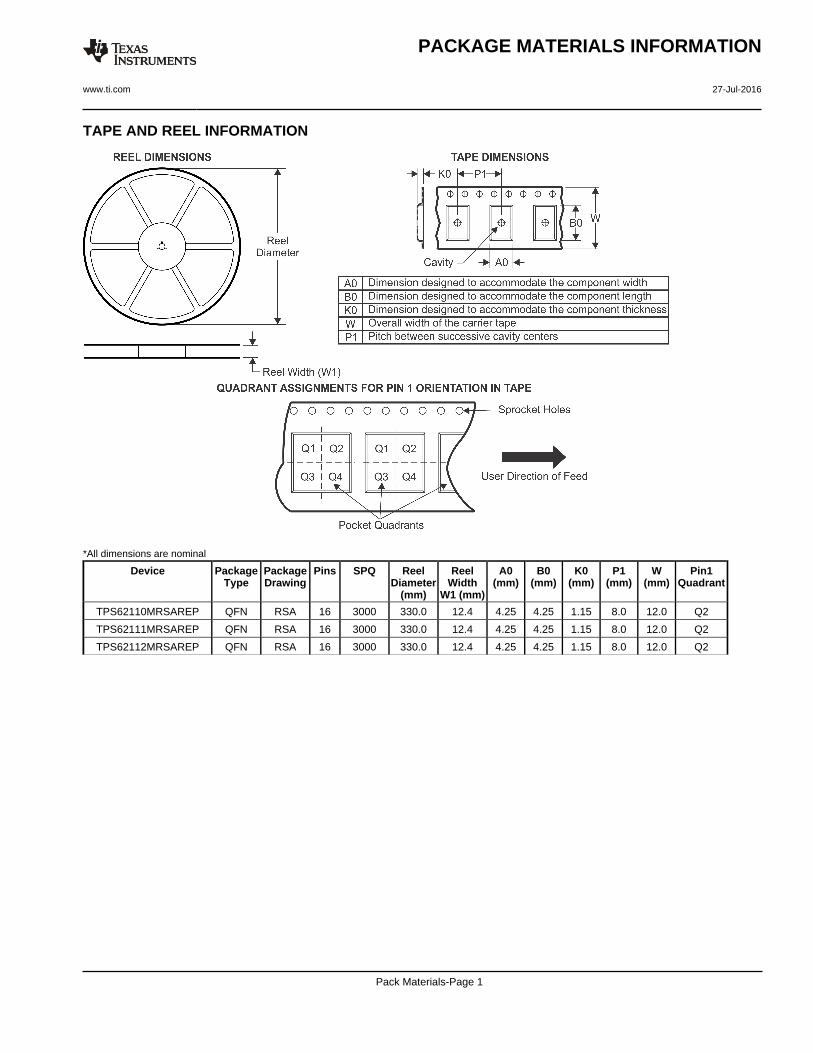
TAPE AND REEL INFORMATION
*All dimensions are nominal
Device PackageType
PackageDrawing
Pins SPQ ReelDiameter
(mm)
ReelWidth
W1 (mm)
A0(mm)
B0(mm)
K0(mm)
P1(mm)
W(mm)
Pin1Quadrant
TPS62110MRSAREP QFN RSA 16 3000 330.0 12.4 4.25 4.25 1.15 8.0 12.0 Q2
TPS62111MRSAREP QFN RSA 16 3000 330.0 12.4 4.25 4.25 1.15 8.0 12.0 Q2
TPS62112MRSAREP QFN RSA 16 3000 330.0 12.4 4.25 4.25 1.15 8.0 12.0 Q2
PACKAGE MATERIALS INFORMATION
www.ti.com 27-Jul-2016
Pack Materials-Page 1
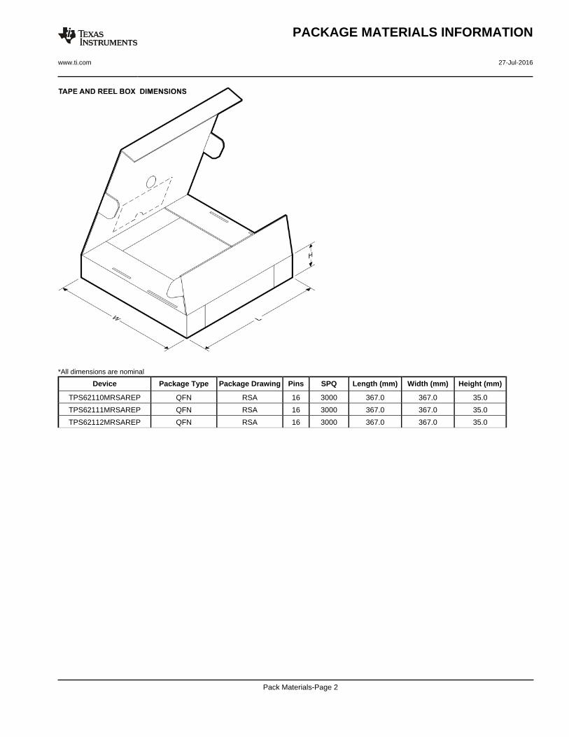
*All dimensions are nominal
Device Package Type Package Drawing Pins SPQ Length (mm) Width (mm) Height (mm)
TPS62110MRSAREP QFN RSA 16 3000 367.0 367.0 35.0
TPS62111MRSAREP QFN RSA 16 3000 367.0 367.0 35.0
TPS62112MRSAREP QFN RSA 16 3000 367.0 367.0 35.0
PACKAGE MATERIALS INFORMATION
www.ti.com 27-Jul-2016
Pack Materials-Page 2
IMPORTANT NOTICE
Texas Instruments Incorporated and its subsidiaries (TI) reserve the right to make corrections, enhancements, improvements and otherchanges to its semiconductor products and services per JESD46, latest issue, and to discontinue any product or service per JESD48, latestissue. Buyers should obtain the latest relevant information before placing orders and should verify that such information is current andcomplete. All semiconductor products (also referred to herein as “components”) are sold subject to TI’s terms and conditions of salesupplied at the time of order acknowledgment.TI warrants performance of its components to the specifications applicable at the time of sale, in accordance with the warranty in TI’s termsand conditions of sale of semiconductor products. Testing and other quality control techniques are used to the extent TI deems necessaryto support this warranty. Except where mandated by applicable law, testing of all parameters of each component is not necessarilyperformed.TI assumes no liability for applications assistance or the design of Buyers’ products. Buyers are responsible for their products andapplications using TI components. To minimize the risks associated with Buyers’ products and applications, Buyers should provideadequate design and operating safeguards.TI does not warrant or represent that any license, either express or implied, is granted under any patent right, copyright, mask work right, orother intellectual property right relating to any combination, machine, or process in which TI components or services are used. Informationpublished by TI regarding third-party products or services does not constitute a license to use such products or services or a warranty orendorsement thereof. Use of such information may require a license from a third party under the patents or other intellectual property of thethird party, or a license from TI under the patents or other intellectual property of TI.Reproduction of significant portions of TI information in TI data books or data sheets is permissible only if reproduction is without alterationand is accompanied by all associated warranties, conditions, limitations, and notices. TI is not responsible or liable for such altereddocumentation. Information of third parties may be subject to additional restrictions.Resale of TI components or services with statements different from or beyond the parameters stated by TI for that component or servicevoids all express and any implied warranties for the associated TI component or service and is an unfair and deceptive business practice.TI is not responsible or liable for any such statements.Buyer acknowledges and agrees that it is solely responsible for compliance with all legal, regulatory and safety-related requirementsconcerning its products, and any use of TI components in its applications, notwithstanding any applications-related information or supportthat may be provided by TI. Buyer represents and agrees that it has all the necessary expertise to create and implement safeguards whichanticipate dangerous consequences of failures, monitor failures and their consequences, lessen the likelihood of failures that might causeharm and take appropriate remedial actions. Buyer will fully indemnify TI and its representatives against any damages arising out of the useof any TI components in safety-critical applications.In some cases, TI components may be promoted specifically to facilitate safety-related applications. With such components, TI’s goal is tohelp enable customers to design and create their own end-product solutions that meet applicable functional safety standards andrequirements. Nonetheless, such components are subject to these terms.No TI components are authorized for use in FDA Class III (or similar life-critical medical equipment) unless authorized officers of the partieshave executed a special agreement specifically governing such use.Only those TI components which TI has specifically designated as military grade or “enhanced plastic” are designed and intended for use inmilitary/aerospace applications or environments. Buyer acknowledges and agrees that any military or aerospace use of TI componentswhich have not been so designated is solely at the Buyer's risk, and that Buyer is solely responsible for compliance with all legal andregulatory requirements in connection with such use.TI has specifically designated certain components as meeting ISO/TS16949 requirements, mainly for automotive use. In any case of use ofnon-designated products, TI will not be responsible for any failure to meet ISO/TS16949.
Products ApplicationsAudio www.ti.com/audio Automotive and Transportation www.ti.com/automotiveAmplifiers amplifier.ti.com Communications and Telecom www.ti.com/communicationsData Converters dataconverter.ti.com Computers and Peripherals www.ti.com/computersDLP® Products www.dlp.com Consumer Electronics www.ti.com/consumer-appsDSP dsp.ti.com Energy and Lighting www.ti.com/energyClocks and Timers www.ti.com/clocks Industrial www.ti.com/industrialInterface interface.ti.com Medical www.ti.com/medicalLogic logic.ti.com Security www.ti.com/securityPower Mgmt power.ti.com Space, Avionics and Defense www.ti.com/space-avionics-defenseMicrocontrollers microcontroller.ti.com Video and Imaging www.ti.com/videoRFID www.ti-rfid.comOMAP Applications Processors www.ti.com/omap TI E2E Community e2e.ti.comWireless Connectivity www.ti.com/wirelessconnectivity
Mailing Address: Texas Instruments, Post Office Box 655303, Dallas, Texas 75265Copyright © 2016, Texas Instruments Incorporated