Embed Size (px)
Citation preview

TOPOLOGY ZERO:
ADVANCING THEORY AND EXPERIMENTATION FOR
POWER ELECTRONICS EDUCATION
by
Federico Luchino
Ing., Universidad Tecnologica Nacional (Cordoba), 2005
a Thesis submitted in partial fulfillment
of the requirements for the degree of
Master of Applied Science
in the
School of Engineering Science
Faculty of Applied Sciences
c⃝ Federico Luchino 2012
SIMON FRASER UNIVERSITY
Fall 2012
All rights reserved.
However, in accordance with the Copyright Act of Canada, this work may be
reproduced without authorization under the conditions for “Fair Dealing.”
Therefore, limited reproduction of this work for the purposes of private study,
research, criticism, review and news reporting is likely to be in accordance
with the law, particularly if cited appropriately.

APPROVAL
Name: Federico Luchino
Degree: Master of Applied Science
Title of Thesis: Topology Zero: Advancing Theory and Experimentation for
Power Electronics Education
Examining Committee: Dr. Woo Soo Kim
Chair
Dr. Martin Ordonez, Senior Supervisor,
Assistant Professor
Dr. Ahmad Rad, Supervisor,
Professor
Dr. Mehrdad Moallem, Internal Examiner,
Professor
Date Approved: October 1st, 2012
ii

Partial Copyright Licence
iii

Abstract
For decades, power electronics education has been based on the fundamentals of three ba-
sic topologies: buck, boost, and buck-boost. This thesis presents the analytical framework
for the Topology Zero, a general circuit topology that integrates the basic topologies and
provides significant insight into the behaviour of converters. As demonstrated, many topolo-
gies are just particular cases of the Topology Zero, an important contribution towards the
understanding, integration, and conceptualization of topologies. The investigation includes
steady-state, small-signal, and frequency response analysis. The Topology Zero is physically
implemented as an educational system. Experimental results are presented to show control
applications and power losses analysis using the educational system. The steady-state and
dynamic analyses of the Topology Zero provide profuse proof of its suitability as an integra-
tive topology, and of its ability to be indirectly controlled. As well, the implementation of
the Topology Zero within an experimentation system is explained and application examples
are provided.
Keywords: power electronics; education; converter
iv

To the exceptional people who marked my life
v

“When the dogs bark we know we are riding on horseback”
Johann Wolfgang von Goethe
vi

Acknowledgments
I would like to greatly thank my supervisor Dr. Martın Ordonez for accepting me as one of
his Masters students and giving me the opportunity to work with him. I have to acknowledge
his support throughout the challenging and rewarding path of the Master’s program.
I would like to express my sincerest gratitude to my colleagues at the Renewable and
Alternative Power Laboratory for the amazing and amusing group we formed and for the
knowledge they kindly shared with me.
I would like to particularly thank Nancy, the only reason this document exists.
The last but foremost, I would like to really thank my family, who are the ones I care
for the most, especially my parents Ana and Clemar, who unconditionally supported me
through the years in the decisions that I have made.
vii

Contents
Approval ii
Declaration of Partial Copyright License iii
Abstract iv
Dedication v
Quotation vi
Acknowledgments vii
Contents viii
List of Tables xi
List of Figures xii
Nomenclature xv
1 Introduction 1
1.1 Motivation . . . . . . . . . . . . . . . . . . . . . . . . . . . . . . . . . . . . . 1
1.2 Existing Methodologies in Education . . . . . . . . . . . . . . . . . . . . . . . 3
1.3 Contribution of This Thesis . . . . . . . . . . . . . . . . . . . . . . . . . . . . 5
1.4 Thesis Outline . . . . . . . . . . . . . . . . . . . . . . . . . . . . . . . . . . . 5
2 Topology Zero: Steady-state Analysis 7
2.1 Step-down Configurations . . . . . . . . . . . . . . . . . . . . . . . . . . . . . 9
viii

2.2 Step-up Configurations . . . . . . . . . . . . . . . . . . . . . . . . . . . . . . . 12
2.3 Step-down-step-up Configurations . . . . . . . . . . . . . . . . . . . . . . . . 15
2.4 Alternative Derivation . . . . . . . . . . . . . . . . . . . . . . . . . . . . . . . 18
2.5 A General Topology: One Topology to Rule Them All . . . . . . . . . . . . . 20
2.5.1 Buck Converter . . . . . . . . . . . . . . . . . . . . . . . . . . . . . . . 21
2.5.2 Boost Converter . . . . . . . . . . . . . . . . . . . . . . . . . . . . . . 21
2.5.3 Buck-boost Converter . . . . . . . . . . . . . . . . . . . . . . . . . . . 22
2.6 Summary . . . . . . . . . . . . . . . . . . . . . . . . . . . . . . . . . . . . . . 23
3 Topology Zero: Small-signal Analysis 25
3.1 Topology Zero Step-down Configurations . . . . . . . . . . . . . . . . . . . . . 26
3.1.1 Step-down Configuration with Negative Reference . . . . . . . . . . . 26
3.1.2 Step-down Configuration with Positive Reference . . . . . . . . . . . . 34
3.2 Topology Zero Step-up Configurations . . . . . . . . . . . . . . . . . . . . . . 39
3.2.1 Step-up Configuration with Negative Reference . . . . . . . . . . . . . 39
3.2.2 Step-up Configuration with Positive Reference . . . . . . . . . . . . . 48
3.3 Topology Zero Step-down-step-up Configurations . . . . . . . . . . . . . . . . 57
3.3.1 Step-down-step-up Configuration with Negative Reference . . . . . . . 57
3.3.2 Step-down-step-up Configuration with Positive Reference . . . . . . . 66
3.4 Summary . . . . . . . . . . . . . . . . . . . . . . . . . . . . . . . . . . . . . . 74
4 Topology Zero: Possible Configurations and Power losses 76
4.1 Topology Zero Possible Configurations . . . . . . . . . . . . . . . . . . . . . . 76
4.1.1 Topology Zero Step-down Configurations . . . . . . . . . . . . . . . . 77
4.1.2 Topology Zero Step-up Configurations . . . . . . . . . . . . . . . . . . 80
4.1.3 Topology Zero Step-down-step-up Configurations . . . . . . . . . . . . 82
4.1.4 Topology Zero Bridge Configurations . . . . . . . . . . . . . . . . . . . 84
4.2 Topology Zero Power Losses . . . . . . . . . . . . . . . . . . . . . . . . . . . . 86
4.2.1 Inductor Losses in Step-down Configuration . . . . . . . . . . . . . . . 86
4.2.2 Semiconductor Losses in Step-down Configuration . . . . . . . . . . . 88
4.2.2.1 Transitor and Diode Losses . . . . . . . . . . . . . . . . . . . 88
4.2.2.2 Transistors Losses . . . . . . . . . . . . . . . . . . . . . . . . 89
4.2.3 Inductor Losses in Step-up Configuration . . . . . . . . . . . . . . . . 89
4.2.4 Semiconductor Losses in Step-up Configuration . . . . . . . . . . . . . 90
ix

4.2.4.1 Transistor and Diode Losses . . . . . . . . . . . . . . . . . . 90
4.2.4.2 Transistors Losses . . . . . . . . . . . . . . . . . . . . . . . . 91
4.2.5 Inductor Losses in Step-down-step-up Configuration . . . . . . . . . . 91
4.2.6 Semiconductor Losses in Step-down-step-up Configuration . . . . . . . 93
4.2.6.1 Transitor and Diode Losses . . . . . . . . . . . . . . . . . . . 93
4.2.6.2 Transistors Losses . . . . . . . . . . . . . . . . . . . . . . . . 94
4.3 Summary . . . . . . . . . . . . . . . . . . . . . . . . . . . . . . . . . . . . . . 94
5 Educational Setup Implementation Based on the Topology Zero 95
5.1 Control and Communication Platform (CCP) . . . . . . . . . . . . . . . . . . 96
5.2 Topology Zero Platform (TZP) . . . . . . . . . . . . . . . . . . . . . . . . . . 99
5.3 Applications . . . . . . . . . . . . . . . . . . . . . . . . . . . . . . . . . . . . . 101
5.3.1 Power Losses Analysis in Power MOSFET . . . . . . . . . . . . . . . . 101
5.3.2 Advanced Control Strategies: Boundary Control of Boost Converter . 105
5.3.3 Planar Transformer Characterization and LLC Converter . . . . . . . 108
5.3.4 Other Applications . . . . . . . . . . . . . . . . . . . . . . . . . . . . . 111
5.4 Summary . . . . . . . . . . . . . . . . . . . . . . . . . . . . . . . . . . . . . . 111
6 Conclusions and Future Work 113
6.1 Conclusions . . . . . . . . . . . . . . . . . . . . . . . . . . . . . . . . . . . . . 113
6.2 Future Work . . . . . . . . . . . . . . . . . . . . . . . . . . . . . . . . . . . . 115
Bibliography 117
x

List of Tables
2.1 Topology Zero DC-DC configurations. . . . . . . . . . . . . . . . . . . . . . . 9
3.1 Step-down configuration parameters . . . . . . . . . . . . . . . . . . . . . . . 31
3.2 Step-down configuration parameters . . . . . . . . . . . . . . . . . . . . . . . 36
3.3 Step-up configuration parameters . . . . . . . . . . . . . . . . . . . . . . . . . 42
3.4 Step-up configuration parameters . . . . . . . . . . . . . . . . . . . . . . . . . 51
3.5 Step-down-step-up configuration parameters . . . . . . . . . . . . . . . . . . . 60
3.6 Step-down-step-up configuration parameters . . . . . . . . . . . . . . . . . . . 68
xi

List of Figures
1.1 Topology Zero. . . . . . . . . . . . . . . . . . . . . . . . . . . . . . . . . . . . 2
2.1 Topology Zero. . . . . . . . . . . . . . . . . . . . . . . . . . . . . . . . . . . . 8
2.2 Switching cycle. . . . . . . . . . . . . . . . . . . . . . . . . . . . . . . . . . . . 8
2.3 Step-down configuration with negative reference. . . . . . . . . . . . . . . . . 10
2.4 Step-down configuration steady-state waveforms. (a) Switch position. (b)
Inductor current (iL) and voltage (vL). (c) C2 current (iC2) and voltage (vC2). 10
2.5 Step-down configuration with positive reference. . . . . . . . . . . . . . . . . 11
2.6 Step-down configuration steady-state waveforms. (a) Switch position. (b)
Inductor current (iL) and voltage (vL). (c) C1 current (iC1) and voltage (vC1). 12
2.7 Step-up configuration with negative reference. . . . . . . . . . . . . . . . . . . 13
2.8 Step-up configuration steady-state waveforms. (a) Switch position. (b) In-
ductor current (iL) and voltage (vL). (c) C3 current (iC3) and voltage (vC3). 13
2.9 Step-up configuration with positive reference. . . . . . . . . . . . . . . . . . . 14
2.10 Step-up configuration steady-state waveforms. (a) Switch position. (b) In-
ductor current (iL) and voltage (iL). (c) C3 current (iC3) and voltage (vC3). . 15
2.11 Step-down-step-up configuration with negative reference. . . . . . . . . . . . . 16
2.12 Step-down-step-up configuration steady-state waveforms. (a) Switch posi-
tion. (b) Inductor current (iL) and voltage (vL). (c) C2 current (iC2) and
voltage (vC2). . . . . . . . . . . . . . . . . . . . . . . . . . . . . . . . . . . . . 16
2.13 Step-down-step-up configuration with positive reference. . . . . . . . . . . . . 17
2.14 Step-down-step-up configuration steady-state waveforms. (a) Switch posi-
tion. (b) Inductor current (iL) and voltage (vL). (c) C1 current (iC1) and
voltage (vC1). . . . . . . . . . . . . . . . . . . . . . . . . . . . . . . . . . . . . 18
2.15 Relationship among conversions with Topology Zero. . . . . . . . . . . . . . . 20
xii

2.16 Buck converter. . . . . . . . . . . . . . . . . . . . . . . . . . . . . . . . . . . . 21
2.17 Boost converter. . . . . . . . . . . . . . . . . . . . . . . . . . . . . . . . . . . 22
2.18 Buck-boost converter. . . . . . . . . . . . . . . . . . . . . . . . . . . . . . . . 23
3.1 Step-down configuration equivalent circuits. . . . . . . . . . . . . . . . . . . . 26
3.2 Frequency responses for step-down configuration with negative reference. . . . 32
3.3 Step responses for step-down configuration with negative reference. . . . . . . 33
3.4 Step-down configuration equivalent circuits. . . . . . . . . . . . . . . . . . . . 34
3.5 Frequency responses for step-down configuration with positive reference. . . . 37
3.6 Step responses for step-down configuration with negative reference. . . . . . . 38
3.7 Step-up configuration equivalent circuits. . . . . . . . . . . . . . . . . . . . . 39
3.8 Frequency responses for step-up configuration with negative reference. . . . . 44
3.9 Step responses for step-up configuration with negative reference. . . . . . . . 47
3.10 Step-up configuration equivalent circuits. . . . . . . . . . . . . . . . . . . . . 49
3.11 Frequency responses for step-up configuration with positive reference. . . . . 53
3.12 Step responses for step-up configuration with positive reference. . . . . . . . . 56
3.13 Step-down-step-up configuration equivalent circuits. . . . . . . . . . . . . . . 58
3.14 Frequency responses for step-down-step-up configuration with negative refer-
ence. . . . . . . . . . . . . . . . . . . . . . . . . . . . . . . . . . . . . . . . . . 62
3.15 Step responses for step-down-step-up configuration with negative reference. . 65
3.16 Step-down-step-up configuration equivalent circuits. . . . . . . . . . . . . . . 66
3.17 Frequency responses for step-down-step-up configuration with positive refer-
ence. . . . . . . . . . . . . . . . . . . . . . . . . . . . . . . . . . . . . . . . . . 70
3.18 Step responses for step-down-step-up configuration with positive reference. . . 73
4.1 Topology Zero schematic implemented with MOSFETs. . . . . . . . . . . . . 77
4.2 Step-down configurations implemented with the Topology Zero. . . . . . . . . 79
4.3 Step-up configurations implemented with the Topology Zero. . . . . . . . . . 81
4.4 Step-down-step-up configurations implemented with the Topology Zero. . . . 83
4.5 Bridge configurations implemented with the Topology Zero. . . . . . . . . . . 85
4.6 Equivalent circuits for non-ideal components. . . . . . . . . . . . . . . . . . . 86
4.7 Step-down configuration. . . . . . . . . . . . . . . . . . . . . . . . . . . . . . . 87
4.8 Transfer ratio considering different relationship between load resistance and
resistive copper losses. . . . . . . . . . . . . . . . . . . . . . . . . . . . . . . . 88
xiii

4.9 Step-up configuration. . . . . . . . . . . . . . . . . . . . . . . . . . . . . . . . 89
4.10 Transfer ratio considering different relationship between load resistance and
resistive copper losses. . . . . . . . . . . . . . . . . . . . . . . . . . . . . . . . 90
4.11 Step-down-step-up configuration. . . . . . . . . . . . . . . . . . . . . . . . . . 92
4.12 Transfer ratio considering different relationship between load resistance and
resistive copper losses. . . . . . . . . . . . . . . . . . . . . . . . . . . . . . . . 93
5.1 Power system diagram. . . . . . . . . . . . . . . . . . . . . . . . . . . . . . . . 95
5.2 Control and Communication Platform (CCP). . . . . . . . . . . . . . . . . . . 96
5.3 Control and Communication Platform (CCP). . . . . . . . . . . . . . . . . . . 98
5.4 Power conversion system based on Topology Zero Platforms. . . . . . . . . . 99
5.5 Topology Zero Platform. . . . . . . . . . . . . . . . . . . . . . . . . . . . . . . 101
5.6 Boost converter. . . . . . . . . . . . . . . . . . . . . . . . . . . . . . . . . . . 103
5.7 Drain-source voltage versus gate resistance interaction in the power dissipa-
tion model. . . . . . . . . . . . . . . . . . . . . . . . . . . . . . . . . . . . . . 104
5.8 Drain current versus gate resistance interaction in the power dissipation model.104
5.9 Boost converter based on the Topology Zero Platform. . . . . . . . . . . . . . 106
5.10 Transient response using the NSS for constant current load change: Output
voltage (Ch1), inductor current (Ch2), switch state (Ch3), and output current
(Ch4). . . . . . . . . . . . . . . . . . . . . . . . . . . . . . . . . . . . . . . . . 107
5.11 Transient response using the NSS for resistive load change: Output voltage
(Ch1), inductor current (Ch2), switch state (Ch3), and output current (Ch4). 107
5.12 Full-bridge LLC resonant converter based on the Topology Zero. . . . . . . . 109
5.13 LLC case study waveforms operating in region 1: voltage applied to resonant
tank (Ch1), primary current (Ch2), and secondary current (Ch4). . . . . . . . 110
5.14 LLC case study waveforms operating in region 2: voltage applied to resonant
tank (Ch1), primary current (Ch2), and secondary current (Ch4). . . . . . . . 110
5.15 Inverter with CCP and 2 TZPs. . . . . . . . . . . . . . . . . . . . . . . . . . . 111
xiv

Nomenclature
C Capacitance
D Diode
D, d Duty cycle
FSW Switching frequency
Gvd Control-to-output transfer function
I, i Current
L Inductance
P Power
Q Transistor
R Resistance
SW Switch
TSW Switching period
V , v Voltage
Vi, vi Input voltage
Vo, vo Output voltage
Z Impedance
η Efficiency
xv

d Duty cycle perturbation
i Current perturbation
v Voltage perturbation
A State matrix
B Input matrix
C Output matrix
K Coefficient matrix
u Input vector perturbation
x State vector perturbation
y Output vector perturbation
u Input vector
x State vector
y Output vector
s Laplace variable
t Time
xvi

Chapter 1
Introduction
Power electronics is ubiquitous in everyday people’s lives. For the past couple of decades
it has been evolving at a fast pace, and it is being employed in areas where previously it
was thought impossible. Additionally, the power range of the applications extends from
extremely low power devices (thousandths of Watts) to very high power systems (millions
of Watts). Any consumer electronics or high-power electric devices that do not already
contain state-of-the-art power electronics circuitry probably will soon.
Successful designers of power electronic devices require expertise in several fields of ap-
plied science: analysis of power losses in the switches, heat management, parasitics in the
physical layout of the circuit, electromagnetic noise susceptibility and emission, efficiency,
control and protections, amongst other considerations. The process of learning power elec-
tronics and gaining practical skills in the area typically extends beyond the curriculum of
undergraduate training and requires a number of years of graduate studies and/or industrial
experience.
1.1 Motivation
In spring 2010, when the author started working toward this thesis, there was an urgent
need for custom-made power converters for research purposes in the Renewal and Alternative
Power Laboratory. No existing commercial products were able to meet the requirements for
the particular projects that were performed at the time and are being performed today. In
order to be able to carry out research experimentation in different areas of power electronics,
1
CHAPTER 1. INTRODUCTION 2
a decision was made to develop and implement a modular system based on several inter-
connected power converter platforms according to the topology required for research. As a
result, a number of complex power platforms were implemented. However, there was often
the need for new designs to cover the fast changing, specific needs of the research laboratory.
Therefore, it was resolved to develop a power converter platform with enough flexibility to
be adapted to several topologies without requiring changes in the layout. Furthermore, this
platform should be able to measure, at different key points, voltage and current for each
topology in order to allow the controller to implement suitable control strategies. Simul-
taneously with the development of the flexible platform, the concept of a new integrative
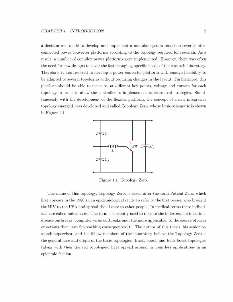
topology emerged, was developed and called Topology Zero, whose basic schematic is shown
in Figure 1.1.
C3
C1
C2
L
SW
Figure 1.1: Topology Zero.
The name of this topology, Topology Zero, is taken after the term Patient Zero, which
first appears in the 1980’s in a epidemiological study to refer to the first person who brought
the HIV to the USA and spread the disease to other people. In medical terms these individ-
uals are called index cases. The term is currently used to refer to the index case of infectious
disease outbreaks, computer virus outbreaks and, the more applicable, to the source of ideas
or actions that have far-reaching consequences [1]. The author of this thesis, his senior re-
search supervisor, and the fellow members of the laboratory believe the Topology Zero is
the general case and origin of the basic topologies. Buck, boost, and buck-boost topologies
(along with their derived topologies) have spread around in countless applications in an
epidemic fashion.

CHAPTER 1. INTRODUCTION 3
1.2 Existing Methodologies in Education
Power electronics is a difficult subject to teach, mainly due to the broad spectrum that it
covers, the theoretical background knowledge that is required from students to understand
every aspect of the topics, and the experimentation needed for a thorough comprehension
of the subject. Several pedagogical approaches to power electronics can be found in the
literature.
Rui et al. [2] propose students develop predefined projects where power electronics con-
cepts are employed, specifically H-bridge for motor control with torque feedback. However,
the spectrum of power electronics applied in these projects is narrow. Other courses aim
to gain good knowledge in component calculation, basic operation of converters and losses
calculation [3], [4]. Even though the knowledge gained is important, these courses focus
on few converters and do not cover control techniques. Web-based reconfigurable power
electronics experimentation platforms are used for teaching and research purposes as well
[5], [6]. The systems are remotely operated and a broad selection of converters can be cho-
sen. The drawbacks of these systems are the implementation costs and mainly, the lack
of contact that students have with the real devices, which could lead them to confuse real
experiments with computer-based simulations. Additionally closed-loop operation can be
applied to the topologies [6]. A similar, more modest approach is found in Hurley et al. [7].
Probst [8] shows a course based on both simulation and hands-on exercises. The simulation
application and the physical platform are developed ad hoc. The system allows a variety of
configurations and implementation of control techniques. However, these control loops are
only basic linear controllers and, the processor employed only performs simple operations.
Williams et al. [9] offer a power electronics system that permits interconnection among
different modules. Although the platform is good for teaching purposes, it has limited use
in research, due to the parasitics that that layout is susceptible to and the circuitry they
use to generate the power signals. Max et al. [10] focus on a real problem in converters
such as parasitics. The exercises are based on one converter and they require students to
design solutions in order to improve the converter operation. Monroy-Berjillos et al. [11]
developed a setup to control thyristors. Showing how mechanical switches can be replaced
by semiconductor devices. The system helps to give an insight into this field of power elec-
tronics, though it does not extend to the other aspects of the subject. Power electronics is
applied to motor control in some courses [12], [13]. They control the devices using virtual

CHAPTER 1. INTRODUCTION 4
instrumentation through a computer. One disadvantage of this systems is the high cost of
the equipment and its maintenance. Web-browser-based simulation tools have been devel-
oped specifically for teaching purposes [14], [15]. The simulation only uses ideal components
to perform the analyses. It is meant to give a qualitative idea of power system operation.
Afterward, the results are compared with more realistic simulation software and educational
setups. Jimenez-Martinez et al. [16] integrate hardware and simulation. The system adapts
into several topologies and is controlled through a computer. However, it operates only
in open-loop mode. Good examples of power electronics systems for educational purposes
have been developed [17], [18], [19], [20]. They offer an adequate variety of topologies to
implement, and sensors of voltage and current are added to allow closed-loop operation.
Robbins et al. [17] employ the switching pole methodology for obtaining different topolo-
gies. Guseme at al. [18] implement a similar switching building block to achieve different
converters. The switching pole and building block are very useful concepts but they are not
a topology. Therefore, they lack the theoretical framework that power converters typically
have, such as steady-state and dynamic analyses. Balog et al. [19] use the blue-box mod-
ule concept, where the modules are first explained in detail, and then employed as closed
modules. Additionally, Jakopovic [20] developed some simulation tools specially for the
courses.
The aforementioned systems cover collectively a broad spectrum of approaches within
power electronics. Some of the approaches focus on simulation or remote experimentation
while others put emphasis on hands-on experiments. Although, the extent of the topics
covered for each of them varies, their individual breadth is somewhat limited. A consider-
ation for the remotely-connected physical setups is the need to have dedicated instruments
attached to the system all the time. Another notable aspect is that not many programs offer
control strategies, neither linear nor non-linear, of power converters. Additionally, analysis
of parasitics is neglected in most of the setups described in the literature. Although there
are good examples of setups, some proposed components, such as the current sensors present
issues with range, frequency bandwidth and noise.
From the above concerns, there is a need to develop a platform able to cover the needs of
both basic power electronics courses and advanced research experimentation. In addition,
some specific requirements have to be met by this setup. First, it has to be flexible in order
to select the topology desired; relatively low cost, with several options for parameter sensing.
Second, it has to provide flexibility in the power devices employed, different technologies of

CHAPTER 1. INTRODUCTION 5
transistors and diodes according to the voltage and current specifications for the topology
chosen. Moreover, isolation and modularity are key features to take into consideration.
In addition, although the components of the platform need to be accessible for teaching
purposes, layout constraints to avoid parasitics have to be observed. Finally, the possibility
of implementing different control techniques is one of the most important aspect of the
development. The consideration of these points in the context of the implementation of the
Topology Zero as an integrative architecture constitute the subject of this thesis.
1.3 Contribution of This Thesis
This work consists of two main sections. The first part of this document explores a new
approach in the style that basic DC-DC switching mode power converters are studied,
introducing the Topology Zero that integrates the three basic conversion topologies, namely
step-down, step-up and step-down-step-up; each of them with more than one option of
implementation. The purpose of the Topology Zero is to facilitate the comprehension of
power converters and to provide a different perspective in the analysis of switching converters
and the way they can be controlled. Different methods of steady-state analysis are derived
to demonstrate the operation of each configuration and equal outcomes are obtained. As
well, a dynamic study in the form of small-signal analysis is performed and the results
are compared with computer-based circuit simulation for frequency and step responses to
confirm the outstanding match between the derivation and the simulation.
In the second part of this document, the physical implementation of the Topology Zero is
discussed. The requirement for this implementation is to obtain a cost-effective and flexible
system that allows different setups to evaluate the basic DC-DC power converters, including
measurements and communication to a personal computer or other similar platforms. The
system is intended to be used for senior undergraduate students in power electronics courses
as well as graduate students in their research projects. Experimental results are presented
to show control applications and power losses analysis using the Topology Zero educational
setup, work that led to a number of IEEE research papers.
1.4 Thesis Outline
This work is organized in the following form:

CHAPTER 1. INTRODUCTION 6
Chapter 2 introduces the Topology Zero and then focuses on the derivation of the steady-
state equations of each of the possible configurations that this topology offers, along with
optional forms of derivation. Additionally, the Topology Zero is compared with well-known
topologies to prove its suitability as a valid converter.
In Chapter 3, small-signal analysis is applied to obtain a transfer function for each
configuration of the Topology Zero and to study their dynamic responses. The results of
the analytical derivation are compared to computer-based circuit simulation to verify their
accuracy.
In Chapter 4, more realistic switching elements are introduced. Many different configura-
tions which involve particular cases of the original Topology Zero are explored. Afterwards,
an introduction to power loss and efficiency is included for different configurations of the
topology.
In Chapter 5, the physical implementation of the educational setup based on the Topol-
ogy Zero is described. The different modules and their corresponding sub-modules are
explained. Additionally, the experimental setups of three IEEE published research articles
using the educational setup based on the Topology Zero are depicted. Afterwards, several
examples of the successful implementation of the Topology Zero are mentioned.
Finally in Chapter 6, conclusions of this work, suggestions for improvement and future
research are discussed.

Chapter 2
Topology Zero: Steady-state
Analysis
This chapter introduces the Topology Zero, a general theoretical framework developed to
study and perform experimentation of basic and derived power converter topologies. The
Topology Zero provides remarkable insight into the steady-state and dynamic analyses of
power converters, resulting in a unified theory that facilitates the comprehension of power
electronics conversion. The Topology Zero consists of a circuit with only three power connec-
tions that allow it to implement step-down, step-up and step-down-step-up DC-DC topolo-
gies, as well as, more complex converters, by only changing the location of the power supply
and the load among those three connections. The basic circuit is shown in Figure 2.1.
The letters A, B, C and D denote the nodes of the Topology Zero, and facilitate their
identification throughout the different configurations.
7

CHAPTER 2. TOPOLOGY ZERO: STEADY-STATE ANALYSIS 8
C3
C1
C2
L0
1
SW v3
v1
v2
C
A
BD
Figure 2.1: Topology Zero.
The power supply and the load can be connected in any of the connection ports indicated
by v1, v2 or v3. In addition, the relationship of these 3 voltages is given by
v3 = v1 + v2 (2.1)
The ratio between the time that the switch is in state 1 (t(1)) over the switching period
(TSW ) is called duty cycle (D) and defined as
D =t(1)
TSW, 0 ≤ D ≤ 1 (2.2)
The graphic representation of the switching period and the duty cycle is shown in Figure 2.2
SW
1 0
TSWt(1) t0
Figure 2.2: Switching cycle.
The different configurations that can be accomplished with the Topology Zero are listed
in Table 2.1
CHAPTER 2. TOPOLOGY ZERO: STEADY-STATE ANALYSIS 9
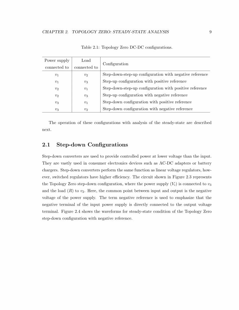
Table 2.1: Topology Zero DC-DC configurations.
Power supply LoadConfiguration
connected to connected to
v1 v2 Step-down-step-up configuration with negative reference
v1 v3 Step-up configuration with positive reference
v2 v1 Step-down-step-up configuration with positive reference
v2 v3 Step-up configuration with negative reference
v3 v1 Step-down configuration with positive reference
v3 v2 Step-down configuration with negative reference
The operation of these configurations with analysis of the steady-state are described
next.
2.1 Step-down Configurations
Step-down converters are used to provide controlled power at lower voltage than the input.
They are vastly used in consumer electronics devices such as AC-DC adapters or battery
chargers. Step-down converters perform the same function as linear voltage regulators, how-
ever, switched regulators have higher efficiency. The circuit shown in Figure 2.3 represents
the Topology Zero step-down configuration, where the power supply (Vi) is connected to v3
and the load (R) to v2. Here, the common point between input and output is the negative
voltage of the power supply. The term negative reference is used to emphasize that the
negative terminal of the input power supply is directly connected to the output voltage
terminal. Figure 2.4 shows the waveforms for steady-state condition of the Topology Zero
step-down configuration with negative reference.

CHAPTER 2. TOPOLOGY ZERO: STEADY-STATE ANALYSIS 10
+
- Vi
C3
C1
C2
L0
1
SW
+
-R
vo
iL
vL
v3
v1
v2
C
A
BD
Figure 2.3: Step-down configuration with negative reference.
-Vo
Vi-Vo
iL
iC2
vL
IL=Io
D·TSW
(a)
(b)
(c)
t
t
t
vC2
Vo
SW
1 0
TSW
A
B
Figure 2.4: Step-down configuration steady-state waveforms. (a) Switch position. (b) In-
ductor current (iL) and voltage (vL). (c) C2 current (iC2) and voltage (vC2).
The voltage across an inductor can be characterized by
vL = LdiL(t)
dt(2.3)
In steady-state the average voltage in the inductor (VL) is equal to 0V . In Figure 2.4b, the
areas A and B are equal to maintain the voltage balance in the inductor. In other words,
the integral of vL in the interval D · TSW is equal to the one in the interval (1−D) · TSW .
(Vi − Vo) ·D · TSW = Vo · (1−D) · TSW (2.4)

CHAPTER 2. TOPOLOGY ZERO: STEADY-STATE ANALYSIS 11
Deriving
Vi ·D − Vo ·D = Vo − Vo ·D
Then, the equation that describes the output-input voltage relationship in steady-state is
Vo
Vi= D (2.5)
It can be stated from (2.5) that the output voltage Vo varies from 0 to Vi as D changes from
0 to 1. The step-down configuration reduces the input voltage by a factor of D.
If the load is connected to v1 instead, the common point between input and output is
the positive connection of the power supply. In this configuration, the inductor is charged
when the switch is in state 0 and the current through it flows in opposite direction compared
to the previous case. The circuit and the signals for this configuration can be observed in
Figure 2.5 and Figure 2.6 respectively.
+
- Vi
C3
C1
C2
L0
1
SW
+
-R
vo
iL
vL
v3
v1
v2
C
A
BD
Figure 2.5: Step-down configuration with positive reference.

CHAPTER 2. TOPOLOGY ZERO: STEADY-STATE ANALYSIS 12
-Vo
Vi-Vo
iL
iC1
vL
IL=Io
(a)
(b)
(c)
t
t
t
vC1
Vo
SW
1 0
D·TSW TSW
A
B
Figure 2.6: Step-down configuration steady-state waveforms. (a) Switch position. (b) In-
ductor current (iL) and voltage (vL). (c) C1 current (iC1) and voltage (vC1).
The inductor voltage balance, in steady-state, can be expressed as
Vo ·D · TSW = (Vi − Vo) · (1−D) · TSW (2.6)
Deriving
Vo ·D = Vi − Vo − Vi ·D + Vo ·DVo = Vi (1−D)
The output-input voltage ratio isVo
Vi= 1−D (2.7)
In this configuration, when D increases, Vo decreases. The variation of the output voltage
in (2.7) responds in opposite fashion compared to (2.5).
2.2 Step-up Configurations
Step-up converters are used to supply output voltage greater than the input. They are em-
ployed in consumer electronics devices, and industrial grade systems such as power factor
correctors (PFC). The circuit shown in Figure 2.7 represents the Topology Zero step-up
configuration, where the power supply is connected to v2 and the load to v3. The reference
point between power supply and load is the negative terminal of the supply. In this con-
figuration the inductor is charged when the switch is in the position 0. Figure 2.8 shows

CHAPTER 2. TOPOLOGY ZERO: STEADY-STATE ANALYSIS 13
the waveforms for steady-state condition of the Topology Zero step-up configuration with
negative reference.
+
-Vi
C3
C1
C2
L0
1
SWiL
+
-R
vo
vL
v3
v1
v2
C
A
BD
Figure 2.7: Step-up configuration with negative reference.
Vi
Vi-Vo
iL
iC3
vL
IL
-Io
(a)
(b)
(c)
t
t
t
vC3
Vo
D·TSW
SW
1 0
TSW
A
B
Figure 2.8: Step-up configuration steady-state waveforms. (a) Switch position. (b) Inductor
current (iL) and voltage (vL). (c) C3 current (iC3) and voltage (vC3).
In Figure 2.8b it can be seen that the voltage balance in the inductor has to be met in
steady-state. Hence the areas A and B are equal. this can be written as follow
(Vo − Vi) ·D · TSW = Vi · (1−D) · TSW (2.8)

CHAPTER 2. TOPOLOGY ZERO: STEADY-STATE ANALYSIS 14
Deriving
Vo ·D − Vi ·D = Vi − Vi ·D
Then, the equation that describes the output-input voltage relationship in steady-state is
Vo
Vi=
1
D(2.9)
Looking at (2.9), it can be observed that the output voltage ranges from Vi to ∞ (ideal),
when D goes from 1 to 0. Hence, this configuration augments the input voltage by a factor
1/D.
If the power supply is connected to v1 instead, the reference point between supply and
load is the positive end of the supply and the inductor is charged when the switch is in state
1, its current flows in opposite direction compared to the previous case. The circuit and the
signals for this configuration can be observed in Figure 2.9 and Figure 2.10 respectively.
+
-Vi
C3
C1
C2
L0
1
SWiL
vL
+
-R
vo
v3
v1
v2
C
A
BD
Figure 2.9: Step-up configuration with positive reference.

CHAPTER 2. TOPOLOGY ZERO: STEADY-STATE ANALYSIS 15
Vi
Vi-Vo
iL
iC3
vL
IL
-Io
(a)
(b)
(c)
t
t
t
vC3
Vo
D·TSW
SW
1 0
TSW
A
B
Figure 2.10: Step-up configuration steady-state waveforms. (a) Switch position. (b) Induc-
tor current (iL) and voltage (iL). (c) C3 current (iC3) and voltage (vC3).
The inductor voltage balance in steady-state, gives
Vi ·D · TSW = (Vo − Vi) · (1−D) · TSW (2.10)
Deriving
Vi ·D = Vo − Vi − Vo ·D + Vi ·DVi = Vo (1−D)
The output-input voltage ratio is then
Vo
Vi=
1
1−D(2.11)
This configuration acts in a complementary mode compared to the step-up with negative
reference. Here the voltage increases from Vi to ∞, when D increases from 0 to 1, as
expressed in (2.11).
2.3 Step-down-step-up Configurations
Step-down-step-up converters may be applied for power supplies where the output can be
either higher or lower than the input voltage, another feature of this converter is that the
load has opposite polarity than the input voltage referred to the common point between
them, unlike the previous configurations. The circuit shown in Figure 2.11 represents the

CHAPTER 2. TOPOLOGY ZERO: STEADY-STATE ANALYSIS 16
Topology Zero step-down-step-up configuration, where the power supply is connected to v1
and the load to v2. In this arrangement, the common point between input and output is the
negative terminal of the power supply. Figure 2.12 shows the waveforms for steady-state
condition of the circuit.
+
-Vi
C3
C1
C2
L0
1
SWiL
vL
+
-R
vo
v3
v1
v2
C
A
BD
Figure 2.11: Step-down-step-up configuration with negative reference.
Vi
-Vo
iL
iC2
vL
IL
-Io
(a)
(b)
(c)
t
t
t
vC2
Vo
D·TSW
SW
1 0
TSW
A
B
Figure 2.12: Step-down-step-up configuration steady-state waveforms. (a) Switch position.
(b) Inductor current (iL) and voltage (vL). (c) C2 current (iC2) and voltage (vC2).
In steady-state, the areas A and B in Figure 2.12b are equal to maintain the voltage

CHAPTER 2. TOPOLOGY ZERO: STEADY-STATE ANALYSIS 17
balance in the inductor. in equation form this is
Vi ·D · TSW = Vo · (1−D) · TSW (2.12)
Then, the equation that describes the output-input voltage relationship in steady-state is
Vo
Vi=
D
1−D(2.13)
Based on (2.13), the output voltage ranges from 0 to ∞, when D goes from 0 to 1. This
configuration can make the output voltage greater or less than the input voltage. The
output voltage equals the input voltage when D = 0.5.
If the power supply is connected to v2 and the load to v1, the common point is the
positive end of the supply. In this configuration, the inductor is charged when the switch
is in the state 0, its current flows in opposite direction compared to the previous case. The
circuit and the signals for this configuration can be observed in Figure 2.13 and Figure 2.14
respectively.
+
-Vi
C3
C1
C2
L0
1
SWiL
vL
+
-R
vo
v3
v1
v2
C
A
BD
Figure 2.13: Step-down-step-up configuration with positive reference.

CHAPTER 2. TOPOLOGY ZERO: STEADY-STATE ANALYSIS 18
Vi
-Vo
iL
iC1
vL
IL
-Io
(a)
(b)
(c)
t
t
t
vC1
Vo
D·TSW
SW
1 0
TSW
A
B
Figure 2.14: Step-down-step-up configuration steady-state waveforms. (a) Switch position.
(b) Inductor current (iL) and voltage (vL). (c) C1 current (iC1) and voltage (vC1).
The inductor voltage balance in steady-state, gives
Vo ·D · TSW = Vi · (1−D) · TSW (2.14)
Then, the output-input voltage ratio is
Vo
Vi=
1−D
D(2.15)
Based on (2.15), the output voltage ranges from 0 to ∞, when D goes from 1 to 0. This
configuration responds in opposite form to the change of the duty cycle than the step-down-
step-up with negative reference.
2.4 Alternative Derivation
Another approach to obtain the equations of the different configurations in steady-state
operation, is combining the transfer ratio of one known topology with (2.1).
Consider the Topology Zero step-down configuration with negative reference shown in
Figure 2.3 with its signals in Figure 2.4 and its transfer ratio is given by (2.5). The equation
is restated using V2 and V3
V2 = D · V3 (2.16)

CHAPTER 2. TOPOLOGY ZERO: STEADY-STATE ANALYSIS 19
Having (2.16) then, V1 as a function of V2 and V3 can be deduced, therefore, another
configuration
V1 = V3 − V2 = V3 −D · V3
then,
V1 = (1−D)V3 (2.17)
This result is equivalent to (2.7) that belongs to the step-down configuration with positive
reference shown in Figure 2.5.
Similarly,
V1 = V3 − V2 =1
DV2 − V2
then,
V1 =(1−D)
DV2 (2.18)
This is equivalent to (2.15) of the step-down-step-up configuration with positive reference
shown in Figure 2.13.
If the other variable is solved in each of (2.16), (2.17) and (2.18), the transfer functions
of the remaining configurations are obtained.
V3 =1
DV2 (2.19)
Equivalent to (2.9), step-up configuration with negative reference.
V3 =1
(1−D)V1 (2.20)
Equivalent to (2.11), step-up configuration with positive reference.
V2 =D
(1−D)V1 (2.21)
Equivalent to (2.13), step-down-step-up configuration with negative reference.
The diagram in Figure 2.15 shows the relationship among the different conversion con-
figurations for the Topology Zero, based on the previous results.

CHAPTER 2. TOPOLOGY ZERO: STEADY-STATE ANALYSIS 20
V3
V1
V2
D
1
D
D
1-D
1-D
D
1-D
1
1-D
Step-downStep-upStep-down-step-up
Figure 2.15: Relationship among conversions with Topology Zero.
These results have an important value in control, due to the fact that a desired config-
uration can be indirectly controlled using one of the other topologies’ algorithm in order to
simplify either the algorithm or the measurement. As an example consider the step-down-
step-up configuration measuring the input voltage (v1 or v2) and controlling v3 to obtain
the output (v2 or v1).
Hitherto, a steady-state study has been carried out to show the different conversion
modes of the Topology Zero. Furthermore, an alternative derivation has been presented,
that takes the result of any known configuration and the other ones can be obtained with
no complication. This derivation has the advantage of allowing indirect control of any
configuration.
2.5 A General Topology: One Topology to Rule Them All
The comparison of the Topology Zero with other known topologies is developed in this
section, highlighting similarities and advantages of using one topology that can operate as
six different converters as it is required.

CHAPTER 2. TOPOLOGY ZERO: STEADY-STATE ANALYSIS 21
2.5.1 Buck Converter
A basic buck converter is shown in Figure 2.16 and its transfer ratio is.
Vo
Vi= k (2.22)
where k is the fraction of the switching period when the inductor is connected to the power
supply.
+
-Vi
L0
1
SW
+
-
R vo
iL
vL
C2
C1
C3
Figure 2.16: Buck converter.
It can be seen that (2.22) is the same as (2.5), Considering k = D. This equation
corresponds to the Topology Zero step-down configuration with negative reference.
In order to implement a classic buck topology, derived from the Topology Zero, the value
of the capacitor C1 should be equal to 0F, as indicated in Figure 2.16 with a grey symbol. As
well, the input voltage source is depicted as an ideal voltage source Vi, which is equivalent
to an infinite capacitor C3 charged at the desired input voltage.
2.5.2 Boost Converter
A boost converter can be represented by the circuit in Figure 2.17 and its transfer ratio is
Vo
Vi=
1
1− k(2.23)

CHAPTER 2. TOPOLOGY ZERO: STEADY-STATE ANALYSIS 22
+
-Vi
L
0
1
SWiL
+
-
R vo
vL
C2
C1
C3
Figure 2.17: Boost converter.
The circuit looks similar to the Topology Zero step-up configuration with negative ref-
erence shown in Figure 2.7. The boost topology is implemented with the Topology Zero by
setting the value of the capacitor C1 to 0F, as indicated with a grey symbol in Figure 2.17.
Additionally, the input voltage source is depicted as an ideal voltage source Vi, which is
equivalent to an infinite capacitor C2 charged at the desired input voltage. Apparently,
the transfer ratio does not match with (2.9). The difference is that k reflects the portion
of the switching period when the inductor is getting charged (when the switch is in 1 in
Figure 2.17) and, on the other hand, D, in (2.9), describes the portion when the inductance
is supplying its energy, in other words, when the switch is in position 1 in Figure 2.7. Thus,
in this case D = 1 − k. The traditional analysis of the known topologies considers k as
the fraction of the switching period when the inductor is charged. That consideration leads
to an inversion in the form the switch operates for the boost converter, compared to the
other two topologies. This constitutes a drawback in the analysis of the basic converters,
due to the fact that, the switch position is not properly consolidated with the rest of the
topologies. It can be stated that the operation of the boost converter is a particular case
of the Topology Zero. The transfer ratio (2.9) reflects the position of the switch that is
compatible with the other two basic configurations.
2.5.3 Buck-boost Converter
A basic buck-boost converter is represented in Figure 2.18 and its transfer ratio is
Vo
Vi=
k
1− k(2.24)

CHAPTER 2. TOPOLOGY ZERO: STEADY-STATE ANALYSIS 23
where k is the fraction of the switching period when the inductor is connected to the power
supply.
+
-Vi
L0
1
SWiL
vL
+
-
Rvo
C3
C1
C2
Figure 2.18: Buck-boost converter.
The buck-boost topology is implemented with the Topology Zero by setting the value of
the capacitor C3 to 0F, as indicated with a grey symbol in Figure 2.18. In addition, the ideal
input voltage source Vi, can be thought as an infinite capacitor C1 charged at the desired
input voltage. The behaviour using the Topology Zero step-down-step-up configuration with
negative reference, shown in Figure 2.13, is the same as the buck-boost topology. It can be
noted that (2.24) has the same form as (2.13).
2.6 Summary
This chapter introduced the Topology Zero as a single circuit to cover the basic switching
DC-DC converter topologies, step-down, step-up and step-down-step-up. The analysis cov-
ered the output-input voltage transfer equation derivation in steady-state and the compar-
ison with known topologies. Additionally, alternative derivation have been demonstrated.
From what above is described, it can be said that the Topology Zero can operate as the
three basic known DC-DC converters, as well as, other configurations (three positive counter
part). Furthermore, these known converters are special cases of the Topology Zero, which
can be achieved by eliminating specific capacitors. The study of a single topology has the
advantage of simplifying the analysis of each configuration and gives a clear insight into the
knowledge of basic power converters. Other advantage of this topology is the possibility of
the development of indirect control strategies, measuring one port to control another.

CHAPTER 2. TOPOLOGY ZERO: STEADY-STATE ANALYSIS 24
In the next chapter dynamic analyses of the Topology Zero are provided for all its config-
urations and the results are verified with the results of computer-based circuit simulations.

Chapter 3
Topology Zero: Small-signal
Analysis
Switching mode converters inevitably require feedback control loops. The output voltage of
the converter must remain constant regardless the variation of the input voltage or output
current requirements. Moreover, the feedback control loop must not produce instability in
the system, and it has to meet some specifications in the transient and the steady-state
operation conditions.
Small-signal analysis for switching converters was first introduced in 1970’s by Middle-
brook et al. [21], who presented a linearized and averaged analysis intended to simplify the
study of switching converters and characterize them, in order to design control strategies.
This important contribution in the form of an analytical procedure has been used ever since
[22]. Profuse literature can be found in power converter analyses where small-signal is ap-
plied to model different converter topologies. For example, the analysis of a three phase
buck rectifier, where steady-state and dynamic studies are carried out [23]. As well, several
switching schemes of a buck converter are analysed [24]. A boost converter in current mode
control is also studied using small-signal [25]. Additionally, the influence of the steady-state
operation over the small-signal condition in buck-boost converters is analysed[26]. When
digital control schemes are to be applied or large-signals are considered, other complemen-
tary methods can be used to characterized power converters. Small-signal analysis gives a
powerful insight into the behaviour of the switching systems and provides the foundation
to control them. The goal of the small-signal procedure is to obtain a valuable transfer
25

CHAPTER 3. TOPOLOGY ZERO: SMALL-SIGNAL ANALYSIS 26
function that models the converter and is further used to design the control loop.
In this chapter, the small-signal analysis is described for the six possible combinations
of the Topology Zero. The analysis starts with the steady-state study of each configuration
and then the small-signal is derived from it. Afterward, comparisons with circuit simulation
are carried out to validate the results.
First, a detailed derivation of the analysis is described for the step-down configuration
with negative reference. Following, the key equations and figures are shown for the other
configurations.
3.1 Topology Zero Step-down Configurations
The small-signal analysis of the step-down configuration with negative reference is first pre-
sented in detail, followed by a shorter derivation of the configuration with positive reference.
3.1.1 Step-down Configuration with Negative Reference
Consider the circuit in Figure 2.3, the equivalent circuits for each position of the switch are
shown in Figure 3.1.
C2
C1
L
vL
+
-v3
iL
iC2
iC1
+
-
R vC2
(a) Switch in position 1 during d(t)TSW .
C2
LvL
+
-v3
iL
iC2
+
-
R vC2
C1
iC1
(b) Switch in position 0 during d′(t)TSW .
Figure 3.1: Step-down configuration equivalent circuits.
Where d′(t) is defines as
d′(t) = 1− d(t) (3.1)
A set of equations can be obtained from the circuit in Figure 3.1a. This circuit represents
the configuration when the switch is in position 1 during d(t)TSW , where d(t) is the time

CHAPTER 3. TOPOLOGY ZERO: SMALL-SIGNAL ANALYSIS 27
variant duty cycle.
vL(t) = LdiL(t)dt = vC1(t)
iC1(t) = C1dvC1(t)
dt = i3(t)− iL(t)
iC2(t) = C2dvC2(t)
dt = i3(t)− vC2(t)R
v3(t) = vC1(t) + vC2(t)
(3.2)
When the switch is in position 0 during d(t)′ TSW , as shown in Figure 3.1b, the equations
that represent the circuit are
vL(t) = LdiL(t)dt = −vC2(t)
iC1(t) = C1dvC1(t)
dt = i3(t)
iC2(t) = C2dvC2(t)
dt = i3(t) + iL(t)− vC2(t)R
v3(t) = vC1(t) + vC2(t)
(3.3)
In matrix form
L 0 0
0 C1 0
0 0 C2
ddt
iL(t)
vC1(t)
vC2(t)
=
0 1 0
−1 0 0
0 0 − 1R
iL(t)
vC1(t)
vC2(t)
+
0
1
1
[i3]
[v3(t)] =[0 1 1
]iL(t)
vC1(t)
vC2(t)
(3.4)
L 0 0
0 C1 0
0 0 C2
ddt
iL(t)
vC1(t)
vC2(t)
=
0 0 −1
0 0 0
1 0 − 1R
iL(t)
vC1(t)
vC2(t)
+
0
1
1
[i3]
[v3(t)] =[0 1 1
]iL(t)
vC1(t)
vC2(t)
(3.5)
(3.4) and (3.5) are written in state-space form, that has the general structure asK ddtx = Ax+Bu
y = Cx(3.6)

CHAPTER 3. TOPOLOGY ZERO: SMALL-SIGNAL ANALYSIS 28
Where
A is the state matrix
B is the input matrix
K is a coefficient matrix
C is the output matrix
x is the state vector
u is the input vector
y is the output vector
The averaged equation model is obtained adding each of the particular equations multiplied
by the fraction of time they are valid.
A = d(t)A1 + d′(t)A2
B = d(t)B1 + d′(t)B2
C = d(t)C1 + d′(t)C2
(3.7)
A = d(t)
0 1 0
−1 0 0
0 0 − 1R
+ d′(t)
0 0 −1
0 0 0
1 0 − 1R
=
0 d(t) −d′(t)
−d(t) 0 0
d′(t) 0 − 1R
(3.8)
B = d(t)
0
1
1
+ d′(t)
0
1
1
=
0
1
1
(3.9)
C = d(t)[0 1 1
]+ d′(t)
[0 1 1
]=
[0 1 1
](3.10)
The averaged model is represented as follows
L 0 0
0 C1 0
0 0 C2
ddt
iL(t)
vC1(t)
vC2(t)
=
0 d(t) −d′(t)
−d(t) 0 0
d′(t) 0 − 1R
iL(t)
vC1(t)
vC2(t)
+
0
1
1
[i3]
[v3(t)] =[0 1 1
]iL(t)
vC1(t)
vC2(t)
(3.11)
If the system is in steady-state the derivative becomes null and a solution can be found
for this equilibrium condition. The variables are considered constant in steady-state and
are represented with capital letters for clarification. 0 = AX+BU
Y = CX(3.12)

CHAPTER 3. TOPOLOGY ZERO: SMALL-SIGNAL ANALYSIS 29
Then (3.11) becomes
[0] =
0 D −D′
−D 0 0
D′ 0 − 1R
IL
VC1
VC2
+
0
1
1
[I3]
[V3] =[0 1 1
]IL
VC1
VC2
(3.13)
Solving X and Y for(3.12) gives X = −A−1BU
Y = −CA−1BU(3.14)
Then (3.13) becomes
X =
IL
VC1
VC2
= −
0 1
D 0
− 1D RD′2
D2 RD′
D
0 RD′
D 1
0
1
1
[I3]
IL
VC1
VC2
=
I3D
I3RD′2
D2 + I3RD′
D
I3RD′
D + I3R
Y = [V3] = −[0 1 1
]0 1
D 0
− 1D RD′2
D2 RD′
D
0 RD′
D 1
0
1
1
[I3]
[V3] =[I3R
D′2
D2 + I3RD′
D + I3RD′
D + I3R]
(3.15)
Solving (3.15) and expressing in algebraic form
IL = I3D
VC1 = I3RD′
D2 = V3D′
VC2 = I3R1D = V3D
V3 = I3R1D2
(3.16)

CHAPTER 3. TOPOLOGY ZERO: SMALL-SIGNAL ANALYSIS 30
The results from (3.16) give the steady-state operation parameters of the configuration, as
well as, its voltage conversion ratio.
The next step for achieving the AC small-signal model is to perturb the system by adding
a small perturbation to the independent variables. These can be then defined as a constant
value plus a small time-dependent variation
d(t) = D + d(t)
v3(t) = V3 + v3(t)(3.17)
Then, the dependent variables will be affected as
iL(t) = IL + iL(t)
vC1(t) = VC1 + vC1(t)
vC2(t) = VC2 + vC2(t)
i3(t) = I3 + i3(t)
(3.18)
Including (3.17) and (3.18) into (3.6) and solving, it produces 3 kind of terms, DC
terms, linear AC terms and nonlinear terms. The derivative of DC terms becomes 0, the
perturbation signal is small thus, the nonlinear terms, that include multiplication of more
than one of the small variable components, can be neglected. Afterward the general form
of the small-signal state-space equation isKdx(t)
dt= Ax(t) +Bu(t) + (A1 −A2)X+ (B1 −B2)Ud(t)
y(t) = Cx(t) + (C1 − C2)Xd(t)(3.19)
For the step-down configuration (3.19) has the following particular solution
L 0 0
0 C1 0
0 0 C2
ddt
iL(t)
vC1(t)
vC2(t)
=
DvC1(t)−D′vC2(t)
−DiL(t)
D′iL(t)− vC2(t)R
+
0
i3(t)
i3(t)
+
V3
−IL
−IL
d(t)
[v3(t)] =[vC1(t) + vC2(t)
] (3.20)
In algebraic form
vL(t) = L diL(t)dt = DvC1(t)−D′vC2(t) + V3d(t)
iC1(t) = C1dvC1(t)
dt = i3(t)−DiL(t)− ILd(t)
iC2(t) = C2dvC2(t)
dt = i3(t) +D′iL(t)− ILd(t)− vC2(t)R
v3(t) = vC1(t) + vC2(t)
(3.21)

CHAPTER 3. TOPOLOGY ZERO: SMALL-SIGNAL ANALYSIS 31
Solving further (3.21) the following equation can be obtained vL(t) = Dv3(t)− vC2(t) + V3d(t)
iL(t) = iC2(t)− iC1(t) +vC2(t)
R
(3.22)
Arranging (3.22) for control-to-output transfer function calculation vL(t) = Dv3(t)− vC2(t) + V3d(t)
iL(t) = (C1 + C2)dvC2(t)
dt − C1dv3(t)dt + vC2(t)
R
(3.23)
To obtain the control-to-output transfer function it is needed to set v3 = 0, this makesdv3(t)dt = 0 as well. Hence, the result is
Gvd(s) =vC2(s)
d(s)
∣∣∣∣∣v3(s)=0
= V31
1 + LsR + (C1 + C2)Ls2
(3.24)
From (3.24) it can be seen that it is a 2nd order system with 2 fixed poles. In addition,
the capacitance C1 adds to C2, resulting in a larger combined total output capacitance.
This characteristic can be exploited to modify the dynamic response of the system without
modifying the output stage of the converter. The only variable that affects the transfer
function is the input voltage, the function is independent of the steady-state operating
point of the converter. The control-to-output transfer function depicts the behaviour of
the output voltage vC2 when perturbations in the control input d occur. This transfer
function is of crucial importance in the characterization of the system performance and, in
the development of control strategies [22]. The function obtained in (3.24) is then compared
with a computer-based simulation of the converter. Frequency and step responses of both,
the transfer function and the circuit are shown in Figure 3.2 and Figure 3.3. The parameters
considered for the numeric example are detailed in Table 3.1. Several curves are obtained
for different values of C1. In addition, the chosen switching frequency FSW is kept high
enough to avoid possible interference with the cutoff frequency of the linear system. This is
one fundamental assumption of small-signal modelling.
Table 3.1: Step-down configuration parameters
FSW = 100KHz R = 1Ω
V3 = 10V L = 100µH
D = 0.75 C2 = 100µF
d = D/50

CHAPTER 3. TOPOLOGY ZERO: SMALL-SIGNAL ANALYSIS 32
−60
−40
−20
0
20
40
Mag
nit
ude
(dB
)
101
102
103
104
105
−180
−135
−90
−45
0
Ph
ase
(deg
)
Frequency (Hz)
C1=0
C1=C2/10
C1=C2/2
C1=C2
(a) Transfer function frequency response.
−40
−20
0
20
40
Mag
nit
ude
(dB
)
101
102
103
104
105
−180
−135
−90
−45
0
Frequency (Hz)
Ph
ase
(deg
)
C1=0
C1=C2/10
C1=C2/2
C1=C2
(b) Simulated circuit open-loop frequency response.
Figure 3.2: Frequency responses for step-down configuration with negative reference.

CHAPTER 3. TOPOLOGY ZERO: SMALL-SIGNAL ANALYSIS 33
0 0.5 1 1.5 2 2.50
0.2
0.4
0.6
0.8
1
1.2
1.4
Time (msec)
Am
pli
tude
C1=0
C1=C2/10
C1=C2/2
C1=C2
(a) Transfer function step response.
0 0.5 1 1.5 2 2.5−0.2
0
0.2
0.4
0.6
0.8
1
1.2
1.4
Time (msec)
Amplitude
C1=0
C1=C2/10
C1=C2/2
C1=C2
(b) Simulated circuit open-loop step response.
Figure 3.3: Step responses for step-down configuration with negative reference.

CHAPTER 3. TOPOLOGY ZERO: SMALL-SIGNAL ANALYSIS 34
As it can be seen from Figure 3.2 and Figure 3.3, the frequency responses are similar
between the transfer function and the circuit simulation for each value of C1. The same
can be observed with the step responses. A particular case is depicted, when C1 = 0 the
Topology Zero becomes a buck converter. The buck converter operation is well known and
implies that C1 does not exist. Nevertheless, the general transfer function of the Topology
Zero remains valid by plugging in C1 = 0.
The inclusion of the capacitance C1 affects the cutoff frequency of the system according
to
f0 =1
2π√
L (C1 + C2)(3.25)
The effects of the frequency displacement can be observed in both the frequency and step
responses. In the frequency response the phase shows a more appreciable change in its shape.
When C1 = C2 the total capacitance doubles the case when C1 = 0, and the cutoff frequency
shifts to the right. In the step response there are changes in the oscillation frequency, the
overshoot amplitude and the settling time. When the capacitance increases, the oscillation
frequency decreases, and the settling time and overshoot amplitude increase.
3.1.2 Step-down Configuration with Positive Reference
Next, the results of the small-signal analysis of the step-down configuration with positive
reference are shown.
The step-down configuration shown in Figure 2.5, presents two equivalent circuits for
each position of the switch, displayed in Figure 3.4
C1
LvL
+
-v3
iL
+
-
R vC1
iC1
C2 iC2
(a) Switch in position 1 during d(t)TSW .
C1
L
vL
+
-v3
iL
+
-
R vC1
iC
C2 iC2
(b) Switch in position 0 during d′(t)TSW .
Figure 3.4: Step-down configuration equivalent circuits.
During the time that the switch is in position 1 (d(t)TSW ), the equations for Figure 3.4a

CHAPTER 3. TOPOLOGY ZERO: SMALL-SIGNAL ANALYSIS 35
are
vL(t) = LdiL(t)dt = −vC1(t)
iC1(t) = C1dvC1(t)
dt = i3(t) + iL(t)− vC1(t)R
iC2(t) = C2dvC2(t)
dt = i3(t)
v3(t) = vC1(t) + vC2(t)
(3.26)
When the switch is in 0, during d(t)′ TSW , the equations for Figure 3.4b
vL(t) = LdiL(t)dt = vC2(t)
iC1(t) = C1dvC1(t)
dt = i3(t)− vC1(t)R
iC2(t) = C2dvC2(t)
dt = i3(t)− iL(t)
v3(t) = vC1(t) + vC2(t)
(3.27)
The averaged model results in
L 0 0
0 C1 0
0 0 C2
ddt
iL(t)
vC1(t)
vC2(t)
=
0 −d(t) d′(t)
d(t) − 1R 0
−d′(t) 0 0
iL(t)
vC1(t)
vC2(t)
+
0
1
1
[i3]
[v3(t)] =[0 1 1
]iL(t)
vC1(t)
vC2(t)
(3.28)
The equations that define the circuit in steady-state are
IL = I3D′
VC1 = I3R1D′ = V3D
′
VC2 = I3RDD′2 = V3D
V3 = I3R1
D′2
(3.29)
The small-signal model has the following expression
L 0 0
0 C1 0
0 0 C2
ddt
iL(t)
vC1(t)
vC2(t)
=
−DvC1(t) +D′vC2(t)
DiL(t)− vC1(t)R
−D′iL(t)
+
0
i3(t)
i3(t)
+
−V3
IL
IL
d(t)
[v3(t)] =[vC1(t) + vC2(t)
] (3.30)

CHAPTER 3. TOPOLOGY ZERO: SMALL-SIGNAL ANALYSIS 36
Solving (3.30) vL(t) = D′v3(t)− vC1(t)− V3d(t)
iL(t) = iC1(t)− iC2(t) +vC1(t)
R
(3.31)
Arranging (3.31) for control-to-output transfer function calculation vL(t) = D′v3(t)− vC1(t) + V3d(t)
iL(t) = (C1 + C2)dvC1(t)
dt − C2dv3(t)dt + vC1(t)
R
(3.32)
To obtain the control-to-output transfer function it is needed to set v3 = 0. The result is
Gvd(s) =vC1(s)
d(s)
∣∣∣∣∣v3(s)=0
= −V31
1 + LsR + (C1 + C2)Ls2
(3.33)
The function obtained in (3.33) is compared with a computer-based simulation of the con-
verter. Frequency and step responses of both, the transfer function and the circuit are
shown in Figure 3.5 and Figure 3.6. The parameters considered for calculation are detailed
in Table 3.2. Several curves are obtained for different values of C2.
Table 3.2: Step-down configuration parameters
FSW = 100KHz R = 1Ω
V3 = 10V L = 100µH
D = 0.75 C1 = 100µF
d = D/50

CHAPTER 3. TOPOLOGY ZERO: SMALL-SIGNAL ANALYSIS 37
−60
−40
−20
0
20
40
Mag
nit
ude
(dB
)
101
102
103
104
105
0
45
90
135
180
Ph
ase
(deg
)
Frequency (Hz)
C2=0
C2=C1/10
C2=C1/2
C2=C1
(a) Transfer function frequency response.
−40
−20
0
20
40
Mag
nit
ude
(dB
)
101
102
103
104
105
0
45
90
135
180
Frequency (Hz)
Ph
ase
(deg
)
C2=0
C2=C1/10
C2=C1/2
C2=C1
(b) Simulated circuit open-loop frequency response.
Figure 3.5: Frequency responses for step-down configuration with positive reference.

CHAPTER 3. TOPOLOGY ZERO: SMALL-SIGNAL ANALYSIS 38
0 0.5 1 1.5 2 2.5−1.4
−1.2
−1
−0.8
−0.6
−0.4
−0.2
0
Time (msec)
Amplitude
C2=0
C2=C1/10
C2=C1/2
C2=C1
(a) Transfer function step response.
0 0.5 1 1.5 2 2.5−1.4
−1.2
−1
−0.8
−0.6
−0.4
−0.2
0
0.2
Time (msec)
Amplitude
C2=0
C2=C1/10
C2=C1/2
C2=C1
(b) Simulated circuit open-loop step response.
Figure 3.6: Step responses for step-down configuration with negative reference.

CHAPTER 3. TOPOLOGY ZERO: SMALL-SIGNAL ANALYSIS 39
The transfer function for the step-down configuration with positive reference have op-
posite response to the one with negative reference, this is shown in the phase graphics and
in the step response. Besides the sign, (3.24) and (3.33) are equal.
The inclusion of the capacitance C2 affects the cutoff frequency of the system according
to
f0 =1
2π√
L (C1 + C2)(3.34)
That is equal to (3.25). The effects of the frequency displacement can be observed in both
the frequency and step responses. The cutoff frequency displaces to the right when the
total capacitance increases, as it is observed in Figure 3.5. As well, when the capacitance
increases, the oscillation frequency decreases, and the settling time and overshoot amplitude
increase, as shown in Figure 3.6.
3.2 Topology Zero Step-up Configurations
Following, the results for the step-up configuration with negative and positive reference are
shown.
3.2.1 Step-up Configuration with Negative Reference
Consider the step-up configuration with negative reference shown in Figure 2.7, the equiv-
alent circuits for each position of the switch are shown in Figure 3.7.
C3
L
vL
+
-v2
iL
+
-
R vC3
iC3
C1
iC1
(a) Switch in position 1 during d(t)TSW .
C3
LvL
+
-v2
iL
+
-
R vC3
iC3C
1
iC1
(b) Switch in position 0 during d′(t)TSW .
Figure 3.7: Step-up configuration equivalent circuits.
A set of equations can be obtained from the circuit in Figure 3.7a. This circuit represents

CHAPTER 3. TOPOLOGY ZERO: SMALL-SIGNAL ANALYSIS 40
the converter when the switch is in position 1 during d(t)TSW
vL(t) = LdiL(t)dt = −vC1(t)
iC1(t) = C1dvC1(t)
dt = iL(t)− i2(t)
iC3(t) = C3dvC3(t)
dt = i2(t)− vC3(t)R
v2(t) = vC3(t)− vC1(t)
(3.35)
When the switch is in position 0 during d(t)′ TSW , as shown in Figure 3.7b, the equations
that represent the circuit are
vL(t) = LdiL(t)dt = vC3(t)− vC1(t)
iC1(t) = C1dvC1(t)
dt = iL(t)− i2(t)
iC3(t) = C3dvC3(t)
dt = i2(t)− iL(t)− vC3(t)R
v2(t) = vC3(t)− vC1(t)
(3.36)
The averaged model results in
L 0 0
0 C1 0
0 0 C3
ddt
iL(t)
vC1(t)
vC3(t)
=
0 −1 d′(t)
1 0 0
−d′(t) 0 − 1R
iL(t)
vC1(t)
vC3(t)
+
0
−1
1
[i2]
[v2(t)] =[0 −1 1
]iL(t)
vC1(t)
vC3(t)
(3.37)
The equations that define the circuit in steady-state are
IL = I2
VC1 = I2RD′D = V2D′
D
VC3 = I2RD = V21D
V2 = I2RD2
(3.38)
CHAPTER 3. TOPOLOGY ZERO: SMALL-SIGNAL ANALYSIS 41
The small-signal model has the following expression
L 0 0
0 C1 0
0 0 C3
ddt
iL(t)
vC1(t)
vC3(t)
=
−vC1(t) +D′vC3(t)
iL(t)
−D′iL(t)− vC3(t)R
+
0
−i2(t)
i2(t)
+
−VC3
0
IL
d(t)
[v2(t)] =[vC3(t)− vC1(t)
] (3.39)
Solving (3.39) vL(t) = v2(t)−DvC3(t)− V3d(t)
DiL(t) = iC3(t) + iC1(t) +vC3(t)
R − ILd(t)(3.40)
Arranging (3.40) for control-to-output transfer function calculation vL(t) = v2(t)−DvC3(t)− V3d(t)
DiL(t) = (C1 + C3)dvC3(t)
dt − C1dv2(t)dt + vC3(t)
R − ILd(t)(3.41)
To obtain the control-to-output transfer function it is needed to set v2 = 0. Hence, the
result is
Gvd(s) =vC3(s)
d(s)
∣∣∣∣∣v2(s)=0
= −VC3
D
1− LsD2R
1 + LsD2R
+ (C1+C3)Ls2
D2
(3.42)
From (3.42) it can be seen that the system has 2 poles and 1 zero whose positions depend
on the steady-state of the converter. In addition, the capacitance C1 adds to C3. Also, the
negative sign in the control-to-output transfer function means that an increase in the duty
cycle produce a decreasing in the output voltage, which is expected.
The zero of the step-up control-to-output transfer function lies in the right-half of the
complex s-plane. The right-half plane zero (RHZ) or nonminimum phase zero produces
phase inversion at high frequency. The magnitude response of a RHZ is similar to a left-
half plane zero, however its phase response is similar to a left-half plane pole. The output
tends to go in the opposite direction at high frequencies compared to the direction at low
frequencies. In a step response, the output goes, initially, in the opposite direction of the
final value. The RHZ have the tendency to create instability in wide-band feedback control
loop, due to the opposite direction that the output voltage follows initially during transients
[22].
The function obtained in (3.42) is then compared with a computer-based simulation of
the converter. Frequency and step responses of both, the transfer function and the circuit

CHAPTER 3. TOPOLOGY ZERO: SMALL-SIGNAL ANALYSIS 42
are shown in Figure 3.8 and Figure 3.9. The parameters considered for calculation are
detailed in Table 3.3. Several curves are obtained for different values of C1 and D.
Table 3.3: Step-up configuration parameters
FSW = 100KHz R = 1Ω
V2 = 10V L = 100µH
d = D/50 C3 = 100µF

CHAPTER 3. TOPOLOGY ZERO: SMALL-SIGNAL ANALYSIS 43
0
10
20
30
40
50
Mag
nit
ude
(dB
)
100
101
102
103
104
105
−90
0
90
180
Ph
ase
(deg
)
Frequency (Hz)
C1=0
C1=C3/10
C1=C3/2
C1=C3
(a) Transfer function frequency response, D = 0.25.
−10
0
10
20
30
40
Mag
nit
ud
e (d
B)
101
102
103
104
105
−90
0
90
180
Ph
ase
(deg
)
Frequency (Hz)
C1=0
C1=C3/10
C1=C3/2
C1=C3
(b) Transfer function frequency response, D = 0.5.

CHAPTER 3. TOPOLOGY ZERO: SMALL-SIGNAL ANALYSIS 44
−20
−10
0
10
20
30
Mag
nit
ude
(dB
)
101
102
103
104
105
−90
0
90
180
Ph
ase
(deg
)
Frequency (Hz)
C1=0
C1=C3/10
C1=C3/2
C1=C3
(c) Transfer function frequency response, D = 0.75.
−10
0
10
20
30
Mag
nit
ude
(dB
)
101
102
103
104
105
−90
0
90
180
Frequency (Hz)
Ph
ase
(deg
)
C1=0
C1=C3/10
C1=C3/2
C1=C3
(d) Simulated circuit open-loop frequency response, D = 0.75.
Figure 3.8: Frequency responses for step-up configuration with negative reference.

CHAPTER 3. TOPOLOGY ZERO: SMALL-SIGNAL ANALYSIS 45
0 0.001 0.002 0.003 0.004 0.005 0.006 0.007 0.008 0.009 0.01−1
−0.8
−0.6
−0.4
−0.2
0
0.2
0.4
0.6
0.8
Time (sec)
Amplitude
C1=0
C1=C3/10
C1=C3/2
C1=C3
(a) Transfer function step response, D = 0.25.
0 0.001 0.002 0.003 0.004 0.005 0.006 0.007 0.008 0.009 0.01−3
−2
−1
0
1
2
3
Time (sec)
Amplitude
C1=0
C1=C3/10
C1=C3/2
C1=C3
(b) Simulated circuit open-loop step response, D = 0.25.

CHAPTER 3. TOPOLOGY ZERO: SMALL-SIGNAL ANALYSIS 46
0 0.5 1 1.5 2 2.5 3 3.5−1.2
−1
−0.8
−0.6
−0.4
−0.2
0
0.2
0.4
0.6
Time (msec)
Amplitude
C1=0
C1=C3/10
C1=C3/2
C1=C3
(c) Transfer function step response, D = 0.5.
0 0.5 1 1.5 2 2.5 3 3.5−2.5
−2
−1.5
−1
−0.5
0
0.5
1
1.5
2
Time (msec)
Amplitude
C1=0
C1=C3/10
C1=C3/2
C1=C3
(d) Simulated circuit open-loop step response, D = 0.5.

CHAPTER 3. TOPOLOGY ZERO: SMALL-SIGNAL ANALYSIS 47
0 0.5 1 1.5 2 2.5−1.4
−1.2
−1
−0.8
−0.6
−0.4
−0.2
0
0.2
0.4
Time (msec)
Amplitude
C1=0
C1=C3/10
C1=C3/2
C1=C3
(e) Transfer function step response, D = 0.75.
0 0.5 1 1.5 2 2.5−2
−1.5
−1
−0.5
0
0.5
1
Time (msec)
Amplitude
C1=0
C1=C3/10
C1=C3/2
C1=C3
(f) Simulated circuit open-loop step response, D = 0.75.
Figure 3.9: Step responses for step-up configuration with negative reference.

CHAPTER 3. TOPOLOGY ZERO: SMALL-SIGNAL ANALYSIS 48
The comparison of the transfer function and the simulation exposes their similarities in
the behaviour. This validates the small-signal analysis and its results to model the Topology
Zero. When C1 = 0 the Topology Zero becomes a boost converter. In other words, the boost
converter is a particular case. The responses for this particular configuration are shown in
the previous curves. The boost topology implies that C1 does not exist. However, the
transfer function of the Topology Zero (3.42) remains valid by plugging in C1 = 0. The
inclusion of the capacitance C1 affects the cutoff frequency of the system according to
f0 =D
2π√
L (C1 + C3)(3.43)
The effects of the frequency displacement can be observed in both the frequency and step
responses. When C1 = C3 the total capacitance doubles the case when C1 = 0, and the
cutoff frequency shifts to the right. Additionally, the frequency response is affected by the
RHZ and the duty cycle in steady-state. The frequency of the RHZ is given by
fz =D2R
2πL(3.44)
Unlike the poles, the position of this root is only dependent on the steady-state of the system.
The relative positions of the zero and poles define the shape of the frequency response for
different values of D. In the magnitude response (Figure 3.8), for lower values of duty cycle
there is not peak in the gain near the cutoff frequency, whereas at high duty cycle, the
peak in magnitude can be observed. The step response of the system, shown in Figure 3.9,
is influenced by the relative position of the zero and the poles, and by the steady-state
condition. At low duty cycle the response is overdamped, and when D increases the system
becomes underdamped. The changes in the undershoot and overshoot amplitudes and times
can be appreciated, as well. A secondary effect that can be observed in the step response
of the circuit simulation in Figure 3.9 is the output ripple variations according to the duty
cycle and the capacitance changes. The bigger the duty cycle the lower the ripple voltage.
Additionally, the inclusion of C1 helps to improve the output ripple of the converter.
3.2.2 Step-up Configuration with Positive Reference
Consider the step-up configuration with positive reference in Figure 2.9, the equivalent
circuits for each position of the switch are shown in Figure 3.10.

CHAPTER 3. TOPOLOGY ZERO: SMALL-SIGNAL ANALYSIS 49
C3
LvL
+
-v1
iL
+
-
R vC3
iC3
C2 iC2
(a) Switch in position 1 during d(t)TSW .
C3
L
vL
+
-v1
iL
+
-
R vC3
iC3
C2 iC2
(b) Switch in position 0 during d′(t)TSW .
Figure 3.10: Step-up configuration equivalent circuits.
A set of equations can be obtained from the circuit in Figure 3.10a. This circuit repre-
sents the converter when the switch is in position 1 during d(t)TSW
vL(t) = LdiL(t)dt = vC3(t)− vC2(t)
iC2(t) = C2dvC2(t)
dt = iL(t)− i1(t)
iC3(t) = C3dvC3(t)
dt = i1(t)− iL(t)− vC3(t)R
v1(t) = vC3(t)− vC2(t)
(3.45)
When the switch is in position 0 during d(t)′ TSW , as shown in Figure 3.10b, the equations
that represent the circuit are
vL(t) = LdiL(t)dt = −vC2(t)
iC2(t) = C2dvC2(t)
dt = iL(t)− i1(t)
iC3(t) = C3dvC3(t)
dt = i1(t)− vC3(t)R
v1(t) = vC3(t)− vC2(t)
(3.46)
The averaged model results in
L 0 0
0 C2 0
0 0 C3
ddt
iL(t)
vC2(t)
vC3(t)
=
0 −1 d(t)
1 0 0
−d(t) 0 − 1R
iL(t)
vC2(t)
vC3(t)
+
0
−1
1
[i1]
[v1(t)] =[0 −1 1
]iL(t)
vC2(t)
vC3(t)
(3.47)

CHAPTER 3. TOPOLOGY ZERO: SMALL-SIGNAL ANALYSIS 50
The equations that define the circuit in steady-state are
IL = I1
VC2 = I1RD′D = V1DD′
VC3 = I1RD′ = V11D′
V1 = I1RD′2
(3.48)
The small-signal model has the following expression
L 0 0
0 C2 0
0 0 C3
ddt
iL(t)
vC2(t)
vC3(t)
=
−vC2(t) +DvC3(t)
iL(t)
−DiL(t)− vC3(t)R
+
0
−i1(t)
i1(t)
+
VC3
0
−IL
d(t)
[v1(t)] =[vC3(t)− vC2(t)
] (3.49)
Solving (3.49) vL(t) = v1(t)−D′vC3(t) + V3d(t)
D′iL(t) = iC2(t) + iC3(t) +vC3(t)
R + ILd(t)(3.50)
Arranging (3.50) for control-to-output transfer function calculation vL(t) = v1(t)−D′vC3(t) + V3d(t)
D′iL(t) = (C2 + C3)dvC3(t)
dt − C2dv1(t)dt + vC3(t)
R − ILd(t)(3.51)
To obtain the control-to-output transfer function it is needed to set v2 = 0. Hence, the
result is
Gvd(s) =vC3(s)
d(s)
∣∣∣∣∣v1(s)=0
=VC3
D′1− Ls
D′2R
1 + LsD′2R + (C2+C3)Ls2
D′2
(3.52)
It can be seen in (3.52) that the system has 2 poles and 1 zero whose positions depend
on the steady-state of the converter. In addition, the capacitance C2 adds to C3. The
function obtained in (3.52) is compared with a computer-based simulation of the converter.
Frequency and step responses of both, the transfer function and the circuit are shown in
Figure 3.11 and Figure 3.12. The parameters considered for the example are detailed in
Table 3.4. Several curves are obtained for different values of C2 and D.

CHAPTER 3. TOPOLOGY ZERO: SMALL-SIGNAL ANALYSIS 51
Table 3.4: Step-up configuration parameters
FSW = 100KHz R = 1Ω
V1 = 10V L = 100µH
d = D/50 C3 = 100µF

CHAPTER 3. TOPOLOGY ZERO: SMALL-SIGNAL ANALYSIS 52
−20
−10
0
10
20
30
Mag
nit
ude
(dB
)
101
102
103
104
105
90
180
270
360
Ph
ase
(deg
)
Frequency (Hz)
C2=0
C2=C3/10
C2=C3/2
C2=C3
(a) Transfer function frequency response, D = 0.25.
0
10
20
30
Mag
nit
ude
(dB
)
101
102
103
104
105
90
180
270
360
Frequency (Hz)
Ph
ase
(deg
)
C2=0
C2=C3/10
C2=C3/2
C2=C3
(b) Simulated circuit open-loop frequency response, D = 0.25.
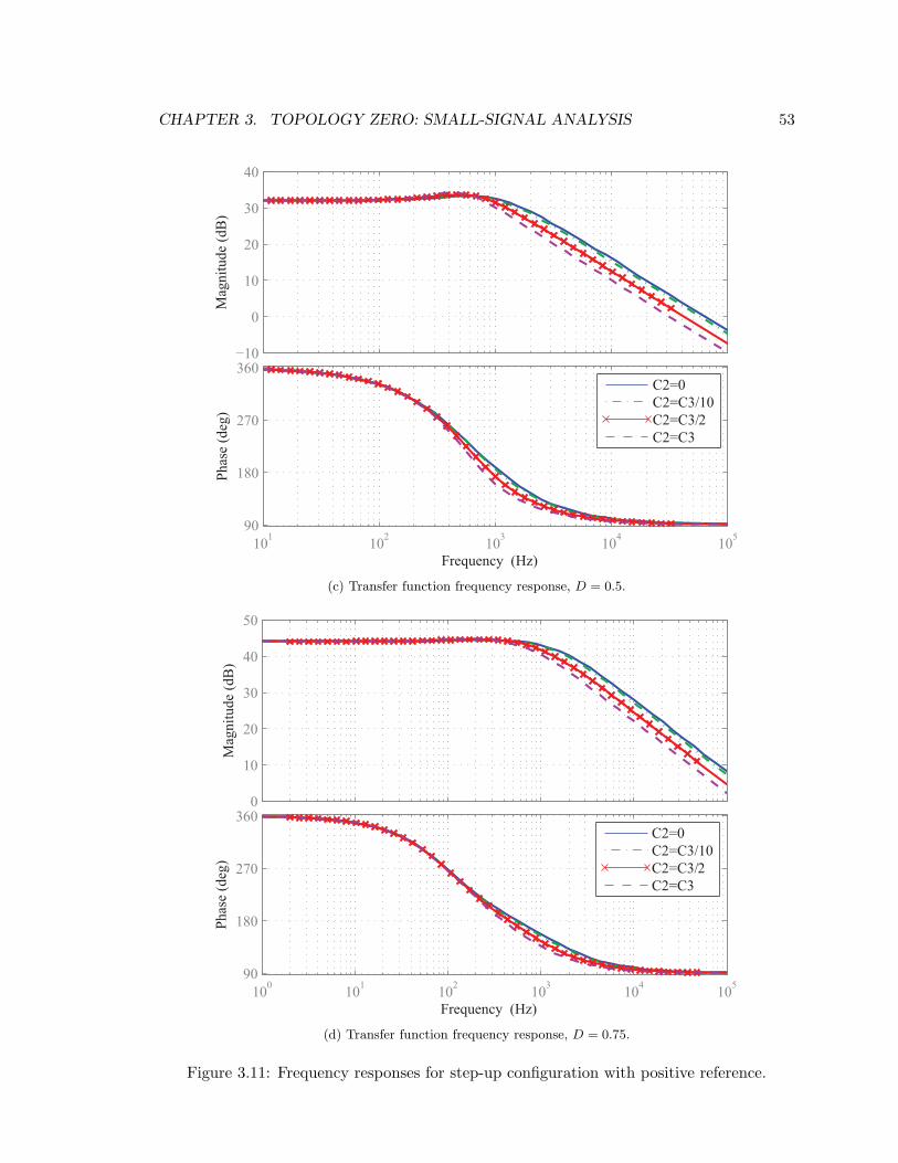
CHAPTER 3. TOPOLOGY ZERO: SMALL-SIGNAL ANALYSIS 53
−10
0
10
20
30
40
Mag
nit
ude
(dB
)
101
102
103
104
105
90
180
270
360
Ph
ase
(deg
)
Frequency (Hz)
C2=0
C2=C3/10
C2=C3/2
C2=C3
(c) Transfer function frequency response, D = 0.5.
0
10
20
30
40
50
Mag
nit
ud
e (d
B)
100
101
102
103
104
105
90
180
270
360
Ph
ase
(deg
)
Frequency (Hz)
C2=0
C2=C3/10
C2=C3/2
C2=C3
(d) Transfer function frequency response, D = 0.75.
Figure 3.11: Frequency responses for step-up configuration with positive reference.

CHAPTER 3. TOPOLOGY ZERO: SMALL-SIGNAL ANALYSIS 54
0 0.5 1 1.5 2 2.5−0.4
−0.2
0
0.2
0.4
0.6
0.8
1
1.2
1.4
Time (msec)
Amplitude
C2=0
C2=C3/10
C2=C3/2
C2=C3
(a) Transfer function step response, D = 0.25.
0 0.5 1 1.5 2 2.5−3
−2
−1
0
1
2
3
Time (msec)
Amplitude
C2=0
C2=C3/10
C2=C3/2
C2=C3
(b) Simulated circuit open-loop step response, D = 0.25.

CHAPTER 3. TOPOLOGY ZERO: SMALL-SIGNAL ANALYSIS 55
0 0.5 1 1.5 2 2.5 3 3.5−0.6
−0.4
−0.2
0
0.2
0.4
0.6
0.8
1
1.2
Time (msec)
Amplitude
C2=0
C2=C3/10
C2=C3/2
C2=C3
(c) Transfer function step response, D = 0.5.
0 0.5 1 1.5 2 2.5 3 3.5−2
−1.5
−1
−0.5
0
0.5
1
1.5
2
2.5
Time (msec)
Amplitude
C2=0
C2=C3/10
C2=C3/2
C2=C3
(d) Simulated circuit open-loop step response, D = 0.5.

CHAPTER 3. TOPOLOGY ZERO: SMALL-SIGNAL ANALYSIS 56
0 0.001 0.002 0.003 0.004 0.005 0.006 0.007 0.008 0.009 0.01−0.8
−0.6
−0.4
−0.2
0
0.2
0.4
0.6
0.8
1
Time (sec)
Amplitude
C2=0
C2=C3/10
C2=C3/2
C2=C3
(e) Transfer function step response, D = 0.75.
0 0.001 0.002 0.003 0.004 0.005 0.006 0.007 0.008 0.009 0.01−1.5
−1
−0.5
0
0.5
1
1.5
2
Time (sec)
Amplitude
C2=0
C2=C3/10
C2=C3/2
C2=C3
(f) Simulated circuit open-loop step response, D = 0.75.
Figure 3.12: Step responses for step-up configuration with positive reference.

CHAPTER 3. TOPOLOGY ZERO: SMALL-SIGNAL ANALYSIS 57
From the previous graphics it can be stated that there is strong correlation between
the transfer function and the simulated circuit behaviour. This validates the small-signal
analysis and its results to model the Topology Zero. The inclusion of the capacitance C2
affects the cutoff frequency of the system according to
f0 =D′
2π√
L (C2 + C3)(3.53)
The effects of the frequency displacement can be observed in both the frequency and step
responses. When C2 increases, the cutoff frequency decreases. Additionally, the frequency
response is affected by the RHZ and the duty cycle in steady-state. The frequency of the
RHZ is given by
fz =D′2R
2πL(3.54)
The relative positions of the zero and poles define the shape of the frequency response for
different values of D. In the magnitude response (Figure 3.11), the gain peak near the cutoff
frequency disappear when the duty cycle increases its value. In the step response of the
system, the response changes from underdamped to overdamped when the duty cycle goes
from lower values to higher ones. This can be appreciated in Figure 3.12.
The responses for the Topology Zero in step-up configuration show similarities between
positive and negative reference. Both transfer functions have gain and singularities affected
by the steady-state of the converter. As well, the influence of the right-half plane zero is
observed in the step responses graphics when initially the output voltage goes in opposite
direction of the final value. In addition, one of the difference is that the output voltage
changes in opposite form for either of the configurations when a step in duty cycle is applied.
However the ripple voltage decreases when the duty cycle increases its steady-stated value.
3.3 Topology Zero Step-down-step-up Configurations
The summarized derivation of the small-signal analysis for step-down-step-up operation of
the Topology Zero in its two variants is next presented.
3.3.1 Step-down-step-up Configuration with Negative Reference
Consider the step-down-step-up configuration with negative reference shown in Figure 2.11,
the equivalent circuits for each position of the switch are shown in Figure 3.13.

CHAPTER 3. TOPOLOGY ZERO: SMALL-SIGNAL ANALYSIS 58
C2
LvL
+
-v1
iL
+
-
R vC2
iC2C
3
iC3
(a) Switch in position 1 during d(t)TSW .
C2
LvL
+
-v1
iL i
C2
+
-
R vC2
C3
iC3
(b) Switch in position 0 during d′(t)TSW .
Figure 3.13: Step-down-step-up configuration equivalent circuits.
A set of equations can be obtained from the circuit in Figure 3.13a. This circuit repre-
sents the converter when the switch is in position 1 during d(t)TSW
vL(t) = LdiL(t)dt = vC3(t)− vC2(t)
iC2(t) = C2dvC2(t)
dt = iL(t)− i1(t)− vC2(t)R
iC3(t) = C3dvC3(t)
dt = i1(t)− iL(t)
v1(t) = vC3(t)− vC2(t)
(3.55)
When the switch is in position 0 during d(t)′ TSW , as shown in Figure 3.13b, the equations
that represent the circuit are
vL(t) = LdiL(t)dt = −vC2(t)
iC2(t) = C2dvC2(t)
dt = iL(t)− i1(t)− vC2(t)R
iC3(t) = C3dvC3(t)
dt = i1(t)
v1(t) = vC3(t)− vC2(t)
(3.56)
The averaged model results in
L 0 0
0 C2 0
0 0 C3
ddt
iL(t)
vC2(t)
vC3(t)
=
0 −1 d(t)
1 − 1R 0
−d(t) 0 0
iL(t)
vC2(t)
vC3(t)
+
0
−1
1
[i1]
[v1(t)] =[0 −1 1
]iL(t)
vC2(t)
vC3(t)
(3.57)

CHAPTER 3. TOPOLOGY ZERO: SMALL-SIGNAL ANALYSIS 59
The equations that define the circuit in steady-state are
IL = I1D
VC2 = I1RD′
D = V1DD′
VC3 = I1RD′
D2 = V11D′
V1 = I1RD′2
D2
(3.58)
The small-signal model has the following expression
L 0 0
0 C2 0
0 0 C3
ddt
iL(t)
vC2(t)
vC3(t)
=
−vC2(t) +DvC3(t)
iL(t)− vC2(t)R
−DiL(t)
+
0
−i1(t)
i1(t)
+
VC3
0
−IL
d(t)
[v1(t)] =[vC3(t)− vC2(t)
] (3.59)
Solving (3.59) vL(t) = Dv1(t)−D′vC2(t) + VC3d(t)
D′iL(t) = iC2(t) + iC3(t) +vC2(t)
R + ILd(t)(3.60)
Arranging (3.60) for control-to-output transfer function calculation vL(t) = Dv1(t)−D′vC2(t) + VC3d(t)
D′iL(t) = (C2 + C3)dvC2(t)
dt + C3dv1(t)dt + vC2(t)
R + ILd(t)(3.61)
To obtain the control-to-output transfer function it is needed to set v1 = 0. The result is
then
Gvd(s) =vC2(s)
d(s)
∣∣∣∣∣v1(s)=0
=VC3
D′1− DLs
D′2R
1 + LsD′2R + (C2+C3)Ls2
D′2
(3.62)
The system has 2 poles and 1 zero whose positions depend on the steady-state of the
converter. In addition, the capacitance C2 adds to C3. The function obtained in (3.62) is
compared with a simulation of the converter. Frequency and step responses of both, the
transfer function and the circuit are shown in Figure 3.14 and Figure 3.15. The parameters
considered for calculation are detailed in Table 3.5. Several curves are obtained for different
values of C3 and D.

CHAPTER 3. TOPOLOGY ZERO: SMALL-SIGNAL ANALYSIS 60
Table 3.5: Step-down-step-up configuration parameters
FSW = 100KHz R = 1Ω
V1 = 10V L = 100µH
d = D/50 C2 = 100µF

CHAPTER 3. TOPOLOGY ZERO: SMALL-SIGNAL ANALYSIS 61
−30
−20
−10
0
10
20
30
Mag
nit
ude
(dB
)
101
102
103
104
105
90
180
270
360
Ph
ase
(deg
)
Frequency (Hz)
C3=0
C3=C2/10
C3=C2/2
C3=C2
(a) Transfer function frequency response, D = 0.25.
0
10
20
30
40
50
Mag
nit
ud
e (d
B)
100
101
102
103
104
105
90
180
270
360
Ph
ase
(deg
)
Frequency (Hz)
C3=0
C3=C2/10
C3=C2/2
C3=C2
(b) Transfer function frequency response, D = 0.75.

CHAPTER 3. TOPOLOGY ZERO: SMALL-SIGNAL ANALYSIS 62
−20
−10
0
10
20
30
40
Mag
nit
ude
(dB
)
101
102
103
104
105
90
180
270
360
Ph
ase
(deg
)
Frequency (Hz)
C3=0
C3=C2/10
C3=C2/2
C3=C2
(c) Transfer function frequency response, D = 0.5.
0
10
20
30
40
Mag
nit
ude
(dB
)
101
102
103
104
105
90
180
270
360
Frequency (Hz)
Ph
ase
(deg
)
C3=0
C3=C2/10
C3=C2/2
C3=C2
(d) Simulated circuit open-loop frequency response, D = 0.5.
Figure 3.14: Frequency responses for step-down-step-up configuration with negative refer-
ence.

CHAPTER 3. TOPOLOGY ZERO: SMALL-SIGNAL ANALYSIS 63
0 0.5 1 1.5 2 2.5−0.2
0
0.2
0.4
0.6
0.8
1
1.2
Time (msec)
Amplitude
C3=0
C3=C2/10
C3=C2/2
C3=C2
(a) Transfer function step response, D = 0.25.
0 0.5 1 1.5 2 2.5−1
−0.5
0
0.5
1
1.5
2
Time (msec)
Amplitude
C3=0
C3=C2/10
C3=C2/2
C3=C2
(b) Simulated circuit open-loop step response, D = 0.25.

CHAPTER 3. TOPOLOGY ZERO: SMALL-SIGNAL ANALYSIS 64
0 0.5 1 1.5 2 2.5−0.4
−0.2
0
0.2
0.4
0.6
0.8
1
1.2
Time (msec)
Amplitude
C3=0
C3=C2/10
C3=C2/2
C3=C2
(c) Transfer function step response, D = 0.5.
0 0.5 1 1.5 2 2.5−1
−0.5
0
0.5
1
1.5
2
Time (msec)
Amplitude
C3=0
C3=C2/10
C3=C2/2
C3=C2
(d) Simulated circuit open-loop step response, D = 0.5.

CHAPTER 3. TOPOLOGY ZERO: SMALL-SIGNAL ANALYSIS 65
0 0.001 0.002 0.003 0.004 0.005 0.006 0.007 0.008 0.009 0.01−0.6
−0.4
−0.2
0
0.2
0.4
0.6
0.8
1
Time (sec)
Amplitude
C3=0
C3=C2/10
C3=C2/2
C3=C2
(e) Transfer function step response, D = 0.75.
0 0.001 0.002 0.003 0.004 0.005 0.006 0.007 0.008 0.009 0.01−1.5
−1
−0.5
0
0.5
1
1.5
2
Time (sec)
Amplitude
C3=0
C3=C2/10
C3=C2/2
C3=C2
(f) Simulated circuit open-loop step response, D = 0.75.
Figure 3.15: Step responses for step-down-step-up configuration with negative reference.

CHAPTER 3. TOPOLOGY ZERO: SMALL-SIGNAL ANALYSIS 66
The comparison of the transfer function and the simulation exposes their similarities in
the behaviour. This validates the small-signal analysis and its results to model the Topology
Zero. When C3 = 0 the Topology Zero becomes a buck-boost converter. The responses for
this particular configuration are shown in the previous curves. The buck-boost converter
does not consider C3. Nevertheless, (3.62) remains valid with C3 = 0. The inclusion of the
capacitance C3 alters the cutoff frequency, as expressed by
f0 =D′
2π√
L (C2 + C3)(3.63)
The effects of the root shift are seen in the frequency and step responses. When C3 increases,
the cutoff frequency decreases. Additionally, the dynamic response is affected by the RHZ
and the duty cycle in steady-state. The frequency of the RHZ is expressed by
fz =D′2R
2πDL(3.64)
In the magnitude response (Figure 3.14), for lower values of steady-state duty cycle there is
a peak in the gain near the cutoff frequency. The peak reduces when D increases. The step
response of the system is influenced by the relative position of the zero and the poles, and by
the steady-state condition. The response changes from underdamped to overdamped when
D varies form lower to higher values (Figure 3.15). The influence of the RHZ is observed,
as well, when in the step response the output goes initially in opposite direction of the final
value.
3.3.2 Step-down-step-up Configuration with Positive Reference
Consider the step-down-step-up configuration with positive reference shown in Figure 2.13,
the equivalent circuits for each position of the switch are shown in Figure 3.16.
C1
LvL
+
-v2
iL
+
-
R vC1
iC1
C3 iC3
(a) Switch in position 1 during d(t)TSW .
C1
LvL
+
-v2
iL
+
-
R vC1
iC1
C3 iC3
(b) Switch in position 0 during d′(t)TSW .
Figure 3.16: Step-down-step-up configuration equivalent circuits.

CHAPTER 3. TOPOLOGY ZERO: SMALL-SIGNAL ANALYSIS 67
A set of equations can be obtained from the circuit in Figure 3.16a. This circuit repre-
sents the converter when the switch is in position 1 during d(t)TSW .
vL(t) = LdiL(t)dt = −vC1(t)
iC1(t) = C1dvC1(t)
dt = iL(t)− i2(t)− vC1(t)R
iC3(t) = C3dvC3(t)
dt = i2(t)
v2(t) = vC3(t)− vC1(t)
(3.65)
When the switch is in position 0 during d(t)′ TSW , as shown in Figure 3.16b, the equations
that represent the circuit are
vL(t) = LdiL(t)dt = vC3(t)− vC1(t)
iC1(t) = C1dvC1(t)
dt = iL(t)− i2(t)− vC1(t)R
iC3(t) = C3dvC3(t)
dt = i2(t)− iL(t)
v2(t) = vC3(t)− vC1(t)
(3.66)
The averaged model results in
L 0 0
0 C1 0
0 0 C3
ddt
iL(t)
vC1(t)
vC3(t)
=
0 −1 d′(t)
1 − 1R 0
−d′(t) 0 0
iL(t)
vC1(t)
vC3(t)
+
0
−1
1
[i2]
[v2(t)] =[0 −1 1
]iL(t)
vC1(t)
vC3(t)
(3.67)
The equations that define the circuit in steady-state are
IL = I2D′
VC1 = I2RDD′ = V2
D′
D
VC3 = I2RDD′2 = V2
1D
V2 = I2RD2
D′2
(3.68)

CHAPTER 3. TOPOLOGY ZERO: SMALL-SIGNAL ANALYSIS 68
The small-signal model has the following expression
L 0 0
0 C1 0
0 0 C3
ddt
iL(t)
vC1(t)
vC3(t)
=
−vC1(t) +D′vC3(t)
iL(t)− vC1(t)R
−D′iL(t)
+
0
−i2(t)
i2(t)
+
−VC3
0
IL
d(t)
[v2(t)] =[vC3(t)− vC1(t)
] (3.69)
Solving (3.69) vL(t) = D′v2(t)−DvC1(t)− VC3d(t)
DiL(t) = iC1(t) + iC3(t) +vC1(t)
R − ILd(t)(3.70)
Arranging (3.70) for control-to-output transfer function calculation vL(t) = D′v2(t)−DvC1(t)− VC3d(t)
DiL(t) = (C1 + C3)dvC1(t)
dt + C3dv2(t)dt + vC1(t)
R + ILd(t)(3.71)
To obtain the control-to-output transfer function it is needed to set v2 = 0. The result is
then
Gvd(s) =vC1(s)
d(s)
∣∣∣∣∣v2(s)=0
= −VC3
D
1− D′LsD2R
1 + LsD2R
+ (C1+C3)Ls2
D2
(3.72)
The system has 2 poles and 1 zero whose positions depend on the steady-state of the
converter. In addition, the capacitance C1 adds to C3. The function obtained in (3.72) is
compared with a simulation of the converter. Frequency and step responses of both, the
transfer function and the circuit are shown in Figure 3.17 and Figure 3.18. The parameters
considered for calculation are detailed in Table 3.6. Several curves are obtained for different
values of C3 and D.
Table 3.6: Step-down-step-up configuration parameters
FSW = 100KHz R = 1Ω
V2 = 10V L = 100µH
d = D/50 C1 = 100µF

CHAPTER 3. TOPOLOGY ZERO: SMALL-SIGNAL ANALYSIS 69
0
10
20
30
40
50
Mag
nit
ude
(dB
)
100
101
102
103
104
105
−90
0
90
180
Ph
ase
(deg
)
Frequency (Hz)
C3=0
C3=C1/10
C3=C1/2
C3=C1
(a) Transfer function frequency response, D = 0.25.
−30
−20
−10
0
10
20
30
Mag
nit
ude
(dB
)
101
102
103
104
105
−90
0
90
180
Ph
ase
(deg
)
Frequency (Hz)
C3=0
C3=C1/10
C3=C1/2
C3=C1
(b) Transfer function frequency response, D = 0.75.

CHAPTER 3. TOPOLOGY ZERO: SMALL-SIGNAL ANALYSIS 70
−20
0
20
40
Mag
nit
ude
(dB
)
101
102
103
104
105
−90
0
90
180
Ph
ase
(deg
)
Frequency (Hz)
C3=0
C3=C1/10
C3=C1/2
C3=C1
(c) Transfer function frequency response, D = 0.5.
0
10
20
30
40
Mag
nit
ude
(dB
)
101
102
103
104
105
−90
0
90
180
Frequency (Hz)
Ph
ase
(deg
)
C3=0
C3=C1/10
C3=C1/2
C3=C1
(d) Simulated circuit open-loop frequency response, D = 0.5.
Figure 3.17: Frequency responses for step-down-step-up configuration with positive refer-
ence.

CHAPTER 3. TOPOLOGY ZERO: SMALL-SIGNAL ANALYSIS 71
0 0.001 0.002 0.003 0.004 0.005 0.006 0.007 0.008 0.009 0.01−1
−0.8
−0.6
−0.4
−0.2
0
0.2
0.4
0.6
0.8
Time (sec)
Amplitude
C1=0
C1=C3/10
C1=C3/2
C1=C3
(a) Transfer function step response, D = 0.25.
0 0.001 0.002 0.003 0.004 0.005 0.006 0.007 0.008 0.009 0.01−3
−2
−1
0
1
2
3
Time (sec)
Amplitude
C1=0
C1=C3/10
C1=C3/2
C1=C3
(b) Simulated circuit open-loop step response, D = 0.25.

CHAPTER 3. TOPOLOGY ZERO: SMALL-SIGNAL ANALYSIS 72
0 0.5 1 1.5 2 2.5−1.2
−1
−0.8
−0.6
−0.4
−0.2
0
0.2
0.4
Time (msec)
Amplitude
C3=0
C3=C1/10
C3=C1/2
C3=C1
(c) Transfer function step response, D = 0.5.
0 0.5 1 1.5 2 2.5−2
−1.5
−1
−0.5
0
0.5
1
Time (msec)
Amplitude
C3=0
C3=C1/10
C3=C1/2
C3=C1
(d) Simulated circuit open-loop step response, D = 0.5.

CHAPTER 3. TOPOLOGY ZERO: SMALL-SIGNAL ANALYSIS 73
0 0.5 1 1.5 2 2.5−1.2
−1
−0.8
−0.6
−0.4
−0.2
0
0.2
Time (msec)
Amplitude
C3=0
C3=C1/10
C3=C1/2
C3=C1
(e) Transfer function step response, D = 0.75.
0 0.5 1 1.5 2 2.5−1.4
−1.2
−1
−0.8
−0.6
−0.4
−0.2
0
0.2
Time (msec)
Amplitude
C3=0
C3=C1/10
C3=C1/2
C3=C1
(f) Simulated circuit open-loop step response, D = 0.75.
Figure 3.18: Step responses for step-down-step-up configuration with positive reference.

CHAPTER 3. TOPOLOGY ZERO: SMALL-SIGNAL ANALYSIS 74
The transfer function and the simulated circuit show similar behaviours. This confirms
the small-signal analysis and its results as a good approach to model the Topology Zero.
The inclusion of the capacitance C3 alters the cutoff frequency, as expressed by
f0 =D
2π√
L (C1 + C3)(3.73)
The effects of the root shift are seen in the frequency and step responses. When C3 increases,
the cutoff frequency decreases. Additionally, the dynamic response is affected by the RHZ
and the duty cycle in steady-state. The frequency of the RHZ is expressed by
fz =D2R
2πD′L(3.74)
In the magnitude response (Figure 3.17), for higher values of steady-state duty cycle there is
a peak in the gain near the cutoff frequency. The peak reduces when D decreases. The step
response changes from overdamped to underdamped when D varies form lower to higher
values (Figure 3.18). The influence of the RHZ is observed, as well; the output goes initially
in opposite direction of the final value when the duty cycle step happens.
The responses for the Topology Zero in step-down-step-up configuration show similarities
between positive and negative reference. Both transfer functions have gain and singularities
affected by the steady-state of the converter, as well, by the sum of the capacitances. In
addition, the output voltage changes in opposite form for either of the configurations when
a step in duty cycle is applied. The step-down-step-up configuration has a right-half plane
zero in the transfer functions of both negative and positive reference. The influence of the
RHZ is manifested in similar form as in the step-up configuration, when a step in the control
input occurs, initially the output voltage goes in opposite direction of the final value, that
is afterwards reached.
3.4 Summary
This chapter continued the analysis of the Topology Zero started in Chapter 2. However, the
focus here was on its dynamic response. The small-signal derivation showed how is possible
to model the Topology Zero in all its configurations, and how the basic known topologies
are special cases of the Topology Zero, proving that one single circuit can cover the whole
basic configuration spectrum. In addition, some peculiarities in the transfer functions are
mentioned such as the RHZ which needs to be specially considered when control strategies

CHAPTER 3. TOPOLOGY ZERO: SMALL-SIGNAL ANALYSIS 75
are to be designed. As well, in the circuit simulations, the ripple variation can be observed
as a function of the additional capacitance.
In the next chapter, the ideal switch is replaced by realistic semiconductor components
and a broad set of configurations of the Topology Zero are explored. Additionally, an
introduction of power losses is given for the basic conversion configurations.

Chapter 4
Topology Zero: Possible
Configurations and Power losses
In previous chapters the electric components of the Topology Zero were considered ideal
for all the analyses. More realistic elements are introduced in this chapter. First, the
switch is replaced by switching semiconductors. This broaden the possible configurations
for the Topology Zero. Afterwards, passive components are considered non-ideal, and power
losses analysis is introduced for different configurations of the Topology Zero to fulfill the
theoretical study of this topology.
4.1 Topology Zero Possible Configurations
The basic configurations analysed in previous chapter are reconsidered here replacing the
switch by switching semiconductors. As well as, in addition to the multiple topologies that
derive from the Topology Zero, two additional configurations are described. The switching
semiconductors that replace the ideal switch can be two transistors or one transistor and
one diode. The schematic of the implementation of the switch with semiconductors is shown
in Figure 4.1.
76

CHAPTER 4. POSSIBLE CONFIGURATIONS AND POWER LOSSES 77
L
C
A
BD
Q1/D1
Q2/D2
C2
C1
C3
Figure 4.1: Topology Zero schematic implemented with MOSFETs.
The schematic is implemented with two metaloxidesemiconductor field-effect transistor
(MOSFET) that have built-in diodes in the devices. Thus, if the transistors are both
controlled, they act as transistors and the configuration operates in synchronous mode. On
the other hand, if only one of the transistor is controlled, the other one acts as diode,
and the configuration operates in asynchronous mode. Which transistor is controlled in
asynchronous mode depends on the selected configuration. Next, possible configurations of
the Topology Zero are explored.
4.1.1 Topology Zero Step-down Configurations
The Topology Zero step-down configurations implemented with switching semiconductors
permit some variations in the topology operation and control. Two groups can be first
defined according to the reference, negative and positive reference configurations, as stated
previously. The Topology Zero step-down configuration with negative reference group can,
in turn, be divided into synchronous and asynchronous modes of operation.
The Topology Zero step-down configuration with negative reference in synchronous mode
requires the two transistors switching in complementary mode. In this category, some op-
tions can be identified: the step-down configuration and a special case where the capacitance
C1 is set to 0F, resulting in a synchronous buck converter. If the Topology Zero step-down
configuration with negative reference operates in asynchronous mode, only the transistor
Q1 is controlled for switching and, the diode D2 conducts when is forward biased. An
asynchronous configuration is much simpler to control and to physically implement than a

CHAPTER 4. POSSIBLE CONFIGURATIONS AND POWER LOSSES 78
synchronous version, resulting in an acceptable cost efficient end product. The configura-
tions that can be identified in asynchronous mode are the step-down configuration and a
special case with C1 set to 0F, the buck converter in asynchronous mode.
The Topology Zero step-down configuration with positive reference in synchronous mode
employs the two transistors switching in complementary fashion. The options that can be
identified in synchronous mode are the step-down configuration and a special case where
the capacitance C2 is set to 0F. This configuration could be called synchronous inverted
buck converter, for the analogy to the known topology. When the Topology Zero step-down
configuration with positive reference operates in asynchronous mode, the conduction of the
transistor Q2 is controlled and, the diode D1 conducts if it is forward biased. The options in
this operating mode are the step-down and a special case that could be called asynchronous
inverted buck converter.
The Topology Zero step-down configurations above mentioned are summarised in Fig-
ure 4.2.

CHAPTER 4. POSSIBLE CONFIGURATIONS AND POWER LOSSES 79
L
CA
BD
Q1/D1
Q2/D2
C2
C1
i A i C
i B
C3
i Ei D
To
po
log
y Z
ero
Ste
p-d
ow
n n
egat
ive
refe
ren
ce
Asy
nch
ron
ou
s st
ep-d
ow
n n
egat
ive
refe
ren
ce
Bu
ck c
on
ver
ter
Ste
p-d
ow
n p
osi
tiv
e re
fere
nce
Asy
nch
ron
ou
s st
ep-d
ow
n p
osi
tiv
e re
fere
nce
Inv
erte
d B
uck
co
nv
erte
r
+ -
L
R
CA
BD
Q1
Q2
C2
C3
Vo
i A i C
i B
i E
C1
Vi
+ -
+ -
L
R
CA
BD
Q1
D2
C2
C3
Vo
i A i C
i B
i E
C1
Vi
+ -
+ -
L
R
CA
BD
Q1
Q2/D2
C2
C3
Vo
i A i C
i B
i E
Vi
+ -
C1
+ -
L
R
CA
BD
Q1
Q2
C2
C3
Vo
i A i C
i B
C1
Vi
+ -
+ -
L
R
CA
BD
D1
Q2
C2
C3
Vo
i A i C
i B
C1
Vi
+ -
+ -
L
R
CA
BD
Q1/D1
Q2
C2
C3
Vo
i A i C
i B
Vi
+ -
C1
Figure
4.2:
Step-dow
nconfigu
rationsim
plementedwiththeTopologyZero.

CHAPTER 4. POSSIBLE CONFIGURATIONS AND POWER LOSSES 80
4.1.2 Topology Zero Step-up Configurations
Some variations in operation and control can be acquired for the Topology Zero step-up con-
figurations implemented with switching semiconductors. The negative and positive reference
groups can be defined. The Topology Zero step-up configuration with negative reference
group can, in turn, be divided into synchronous and asynchronous modes of operation.
In synchronous mode, the configuration requires the two transistors switching in comple-
mentary mode. The variations that can be found in this operation mode are the Topology
Zero step-up configuration with negative reference and a special case where the capacitance
C1 is set to 0F, the synchronous boost converter. If the Topology Zero step-up configuration
with negative reference operates in asynchronous mode, only the switching of the transistor
Q2 is controlled and, the diode D1 conducts when is forward biased. The configurations
included in the asynchronous mode category are the step-up configuration and a special case
with C1 set to 0F, the boost converter in asynchronous mode.
The Topology Zero step-up configuration with positive reference in synchronous mode
employs the two transistors switching in complementary mode. The options in synchronous
mode are the step-up configuration and a special case where the capacitance C2 is set to 0F.
This configuration could be called synchronous inverted boost converter, for the analogy to
the known topology. When the Topology Zero step-up configuration with positive reference
operates in asynchronous mode, only the conduction of the transistor Q1 is controlled and,
the diode D2 conducts if it is forward biased. The options in this operating mode are the
step-up and a special case that could be called asynchronous inverted boost converter, when
C2 is set to 0F.
The Topology Zero step-up configurations above enumerated are summarised in Fig-
ure 4.3.

CHAPTER 4. POSSIBLE CONFIGURATIONS AND POWER LOSSES 81
L
CA
BD
Q1/D1
Q2/D2
C2
C1
i A i C
i B
C3
i Ei D
To
po
log
y Z
ero
Ste
p-u
p n
egat
ive
refe
ren
ce
Asy
nch
ron
ou
s st
ep-u
p n
egat
ive
refe
ren
ce
Bo
ost
co
nv
erte
r
Ste
p-u
p p
osi
tiv
e re
fere
nce
Asy
nch
ron
ou
s st
ep-u
p p
osi
tiv
e re
fere
nce
Inv
erte
d B
oo
st c
on
ver
ter
+ -L
R
CA
BD
Q1
Q2
C2
Vi
C3
Vo
i A i C
i B
C1
+ -
+ -L
R
CA
BD
Q1/D1
Q2
C2
Vi
C3
Vo
i A i C
i B
+ -
+ -L
R
CA
BD
D1
Q2
C2
Vi
C3
Vo
i A i C
i B
C1
+ -
+ -L
R
CA
BD
Q1
Q2
C2
Vi
C3
Vo
C1
+ -
+ -L
R
CA
BD
Q1
Q2/D2
Vi
C3
Vo
C1
+ -
+ -L
R
CA
BD
Q1
D2
C2
Vi
C3
Vo
C1
+ -
C1
C2
i A i C
i B
i A i C
i B
i A i C
i B
Figure
4.3:
Step-upconfigu
rationsim
plementedwiththeTopologyZero.

CHAPTER 4. POSSIBLE CONFIGURATIONS AND POWER LOSSES 82
4.1.3 Topology Zero Step-down-step-up Configurations
The Topology Zero step-down-step-up configurations implemented with switching semicon-
ductors can be categorized in similar form as the other two basic types of configurations.
The negative and positive reference groups can be defined. The Topology Zero step-down-
step-up configuration with negative reference group can be classified into synchronous and
asynchronous modes.
The Topology Zero step-down-step-up configuration with negative reference in syn-
chronous mode operates with the two transistors switching in complementary mode. In
this group the options identified are the step-down-step-up configuration and a special case
where the capacitance C3 is set to 0F, the synchronous buck-boost converter. If the Topol-
ogy Zero step-down-step-up configuration with negative reference operates in asynchronous
mode, only the switching action of the transistor Q1 is controlled and, the diode D2 con-
ducts when is forward biased. The configurations that can be distinguished in asynchronous
mode are the step-down-step-up configuration and a special case with C3 set to 0F, the
buck-boost converter in asynchronous mode.
The Topology Zero step-down-step-up configuration with positive reference in synchronous
mode shows two variations: the step-down-step-up configuration and a special case where
the capacitance C3 is set to 0F. This configuration could be called synchronous inverted
buck-boost converter. When the Topology Zero step-down-step-up configuration operates
in asynchronous mode, only the conduction of the transistor Q2 is controlled and, the diode
D1 conducts if it is forward biased. The options in this operating mode are the step-down-
step-up and a special case that could be called asynchronous inverted buck-boost converter,
when C3 is set to 0F.
Figure 4.4 summarise the configurations above mentioned of the Topology Zero step-
down-step-up.

CHAPTER 4. POSSIBLE CONFIGURATIONS AND POWER LOSSES 83
L
CA
BD
Q1/D1
Q2/D2
C2
C1
i A i C
i B
C3
i Ei D
Topolo
gy Z
ero
Ste
p-d
ow
n-s
tep-u
p n
egat
ive
refe
rence
Asy
nch
ronous
step
-dow
n-s
tep-u
p n
egat
ive
refe
rence
Buck
-boost
conver
ter
Ste
p-d
ow
n-s
tep-u
p p
osi
tive
refe
rence
Asy
nch
ronous
step
-dow
n-s
tep-u
p p
osi
tive
refe
rence
Inver
ted B
uck
-boost
conver
ter
+ -
L
R
CA
BD
Vi Vo
Q1
Q2
C2
C3
i A i C
i B
i E
C1
+ -
+ -
L
R
CA
BD
ViVo
Q1
Q2
C2
C3
C1
+ -
+ -
L
R
CA
BD
ViVo
Q1/D1
Q2
C2
C1
+ -
+ -
L
R
CA
BD
ViVo
Q2
C2
C3
C1
+ -
+ -
L
R
CA
BD
Vi Vo
Q1
Q2/D2
C2
C3
i A i C
i B
i E
C1
+ -
+ -
L
R
CA
BD
Vi Vo
Q1
C2
C3
i A i C
i B
i E
C1
+ -
D2
D1
C3
i A i C
i B
i A i C
i B
i A i C
i B
Figure
4.4:
Step-dow
n-step-upconfigurationsim
plementedwiththeTopologyZero.

CHAPTER 4. POSSIBLE CONFIGURATIONS AND POWER LOSSES 84
4.1.4 Topology Zero Bridge Configurations
In the physical implementation of the Topology Zero, few changes in the components allow
the operation as converters other than the ones above mentioned, the half-bridge converter
and the full-bridge converter.
Half-bridge converters allow to provide both AC and DC output. In this topology the
two transistors are alternatively in on-state. This converter is used for DC-Motor drives,
inverters and for isolated converters. Furthermore, it is able to work bidirectionally, return-
ing energy from the load to the DC input power supply. In order to implement a half-bridge
converter with the Topology Zero, the inductance needs to be replaced for a load.
Full-bridge converters have similar applications to the half-bridge. However, they employ
4 switches, which allows to have more control in the operation as a converter. The drawback
of this type of converters is the complexity in driving the switches. To implement a full-
bridge converter, two replicas of the Topology Zero are interconnected and their inductances
need to be removed.
In Figure 4.5 the bridge configurations of the Topology Zero are shown.

CHAPTER 4. POSSIBLE CONFIGURATIONS AND POWER LOSSES 85
L
C
A
BD
Q1/D1
Q2/D2
C2
C1
iA
iC
iB
C3
iE
iD
Topology Zero
Half-bridge Configuration
Full-bridge Configuration
Z
C
A
BD
Q1
Q2
C2
Vi
C1
Vo
C3
+
-iB
iD
C
A
B
C
A
B
Z
Vo
Q1
Q2
C3
C2
C1
iB
Q1
Q2
C3
C2
C1
Vi
+
-
Figure 4.5: Bridge configurations implemented with the Topology Zero.

CHAPTER 4. POSSIBLE CONFIGURATIONS AND POWER LOSSES 86
4.2 Topology Zero Power Losses
Real circuits have not ideal elements. Previously, real switches have been introduced to
replace the ideal switch. However, passive components are neither ideal. Real elements pro-
duce losses that are manifested as heat. Next, resistive losses in the inductor and conduction
semiconductor losses are considered. The latter contemplate the configuration working in
asynchronous and in synchronous modes.
Inductors are winded with wire that has an associated resistance. Thus, a simple equiv-
alent circuit for a non-ideal inductor can be thought as series connection of ideal inductance
L and parasitics resistance RL. The conduction power loss in a MOSFET is given by its on
resistance Ron. An equivalent circuit that takes into account a diode conduction power loss
is a series connection of a voltage drop and resistance RD [22]. All these circuits are shown
in Figure 4.6
L RL
(a) Equivalent circuit of a non-
ideal inductor.
Ron
D S
(b) Equivalent cir-
cuit of a MOSFET
in on state.
RL
VD
+ -
A K
(c) Equivalent circuit of a diode
in on state.
Figure 4.6: Equivalent circuits for non-ideal components.
4.2.1 Inductor Losses in Step-down Configuration
Losses in the inductor for the Topology Zero in step-down configuration with negative
reference as shown in Figure 4.7 are next considered.
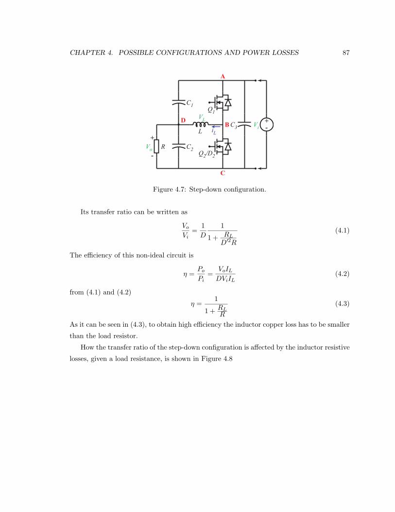
CHAPTER 4. POSSIBLE CONFIGURATIONS AND POWER LOSSES 87
+
-
L
R
C
A
B
C2
Vi
C3
Vo
iL
VLD
C1
Q1
Q2/D2
+
-
Figure 4.7: Step-down configuration.
Its transfer ratio can be written as
Vo
Vi=
1
D
1
1 + RL
D′2R
(4.1)
The efficiency of this non-ideal circuit is
η =Po
Pi=
VoILDViIL
(4.2)
from (4.1) and (4.2)
η =1
1 + RLR
(4.3)
As it can be seen in (4.3), to obtain high efficiency the inductor copper loss has to be smaller
than the load resistor.
How the transfer ratio of the step-down configuration is affected by the inductor resistive
losses, given a load resistance, is shown in Figure 4.8

CHAPTER 4. POSSIBLE CONFIGURATIONS AND POWER LOSSES 88
0 0.2 0.4 0.6 0.8 10
0.1
0.2
0.3
0.4
0.5
0.6
0.7
0.8
0.9
1
D
Vo/V
i
R
L=0
R/RL=10
R/RL=100
Figure 4.8: Transfer ratio considering different relationship between load resistance and
resistive copper losses.
4.2.2 Semiconductor Losses in Step-down Configuration
4.2.2.1 Transitor and Diode Losses
Consider the Topology Zero in step-down configuration shown in Figure 4.7 working in asyn-
chronous mode. The output voltage equation accounting conduction losses in the transistor
and the diode, as well as the inductor copper loss, is given by
Vo = DVi
(1− D′VD2
DVi
)1
1 + RL +DRon1 +D′RD2R
(4.4)
From (4.2) and (4.4), the efficiency of a step-down configuration, considering conduction
and copper losses, can be expressed as
η =1− D′VD2
DVi
1 + RL +DRon1 +D′RD2R
(4.5)
High efficiency can be obtained if DVi ≫ D′VD2 and R ≫ RL +DRon1 +D′RD2

CHAPTER 4. POSSIBLE CONFIGURATIONS AND POWER LOSSES 89
4.2.2.2 Transistors Losses
If the Topology Zero is operating in synchronous mode, that is, two transistors are used as
switches, the output voltage can be expressed as
Vo = DVi1
1 + RL +DRon1 +D′Ron2R
(4.6)
If the transistors are similar, then Ron1 = Ron2 = Ron and (4.6) becomes
Vo = DVi1
1 + RL +RonR
(4.7)
The efficiency is expressed as
η =1
1 + RL +RonR
(4.8)
In order to obtain high efficiency the parasitics resistances have to be kept low.
4.2.3 Inductor Losses in Step-up Configuration
Losses in the inductor for the Topology Zero in step-up configuration with negative reference
as shown in Figure 4.9 are analysed next.
+
-L
R
C
A
B
C2
Vi
C3
Vo
iL
VLD
C1
+
-
Q1/D1
Q2
Figure 4.9: Step-up configuration.
The transfer ratio considering the losses in the inductor is
Vo
Vi=
1
D
1
1 + RL
D2R
(4.9)

CHAPTER 4. POSSIBLE CONFIGURATIONS AND POWER LOSSES 90
The efficiency under this configuration is
η =Po
Pi=
DVoILViIL
(4.10)
Combining (4.9) and (4.10)
η =1
1 + RL
D2R
(4.11)
In order to obtain high efficiency, the inductor copper resistance has to be low.
How the transfer ratio of the step-up configuration is affected by the inductor resistive
losses, given a load resistance, is shown in Figure 4.10.
0 0.2 0.4 0.6 0.8 10
2
4
6
8
10
12
14
16
D
Vo/V
i
R
L=0
R/RL=10
R/RL=100
R/RL=1000
Figure 4.10: Transfer ratio considering different relationship between load resistance and
resistive copper losses.
4.2.4 Semiconductor Losses in Step-up Configuration
4.2.4.1 Transistor and Diode Losses
Consider the Topology Zero in step-up configuration shown in Figure 4.9 working in asyn-
chronous mode. The output voltage equation accounting conduction losses in the transistor
and the diode, as well as the inductor copper loss, is given by
Vo =Vi
D
(1− DVD1
Vi
)1
1 + RL +DRD1 +D′Ron2
D2R
(4.12)

CHAPTER 4. POSSIBLE CONFIGURATIONS AND POWER LOSSES 91
Using (4.10) and (4.12), the efficiency of the step-up configuration is expressed as
η =1− DVD1
Vi
1 + RL +DRD1 +D′Ron2
D2R
(4.13)
High efficiency can be obtained if ViD ≫ VD1 and D2R ≫ RL+DRD1+D′Ron2. Taking into
account that ViD = Vo for an ideal circuit, it can be said that the voltage across the diode
should be much lower than the output voltage.
4.2.4.2 Transistors Losses
If the Topology Zero is operating in synchronous mode, the output voltage can be described
as
Vo =Vi
D
1
1 + RL +DRon1 +D′Ron2
D2R
(4.14)
If the transistors are similar, then Ron1 = Ron2 = Ron and (4.14) becomes
Vo =Vi
D
1
1 + RL +Ron
D2R
(4.15)
The efficiency under this configuration is
η =1
1 + RL +Ron
D2R
(4.16)
In order to obtain high efficiency the parasitics resistances have to be kept low. A consid-
eration about this converter is that the efficiency is affected by the duty cycle.
4.2.5 Inductor Losses in Step-down-step-up Configuration
Losses in the inductor for the Topology Zero in step-down-step-up configuration with neg-
ative reference as shown in Figure 4.11 are analysed next.

CHAPTER 4. POSSIBLE CONFIGURATIONS AND POWER LOSSES 92
+
-
L
R
C
A
BD
C2
C1
iL
VL
C3
Q1
Vi
+
-
Vo
Q2/D2
Figure 4.11: Step-down-step-up configuration.
The transfer ratio considering the losses in the inductor is
Vo =DVi
D′1
1 + RL
D′2R
(4.17)
The efficiency for this setup is given as
η =Po
Pi=
D′VoILDViIL
(4.18)
Incorporating (4.17) into (4.18)
η =1
1 + RL
D′2R
(4.19)
In order to obtain high efficiency, the inductor copper resistance has to be low.
How the transfer ratio of the step-down-step-up configuration is affected by the inductor
resistive losses, given a load resistance, is shown in Figure 4.12.

CHAPTER 4. POSSIBLE CONFIGURATIONS AND POWER LOSSES 93
0 0.2 0.4 0.6 0.8 10
2
4
6
8
10
12
14
16
D
Vo/V
i
R
L=0
R/RL=10
R/RL=100
R/RL=1000
Figure 4.12: Transfer ratio considering different relationship between load resistance and
resistive copper losses.
4.2.6 Semiconductor Losses in Step-down-step-up Configuration
4.2.6.1 Transitor and Diode Losses
Consider the Topology Zero in step-down-step-up configuration shown in Figure 4.11 work-
ing in asynchronous mode. The output voltage equation accounting conduction losses in
the transistor and the diode, as well as the inductor copper loss, is given by
Vo =DVi
D′
(1− D′VD2
DVi
)1
1 + RL +DRon1 +D′RD2
D′2R
(4.20)
Then, using (4.18) and (4.20), the efficiency of a step-down-step-up configuration results in
η =1− D′VD2
DVi
1 + RL +DRon1 +D′RD2
D′2R
(4.21)
To achieve high efficiency, DViD′ ≫ VD2 and D′2R ≫ RL + DRon1 + D′RD2. Taking into
account that DViD′ = Vo for an ideal circuit, it can be assumed that the voltage across the
diode should be much lower than the output voltage.

CHAPTER 4. POSSIBLE CONFIGURATIONS AND POWER LOSSES 94
4.2.6.2 Transistors Losses
If the Topology Zero is operating in synchronous mode, the output voltage is expressed as
Vo =DVi
1−D
1
1 + RL +DRon1 +D′Ron2
D′2R
(4.22)
If the transistors are similar, then Ron1 = Ron2 = Ron and (4.22) becomes
Vo =DVi
1−D
1
1 + RL +Ron
D′2R
(4.23)
The efficiency is expressed as
η =1
1 + RL +Ron
D′2R
(4.24)
In order to obtain high efficiency the parasitics resistances have to be kept low. Like the step-
up configuration, the efficiency is affected by the duty cycle. If the losses are considerable,
it is possible that the converter fails in providing the output estimated.
The analysis given for losses only considered conduction losses in the semiconductors and
resistive losses in the inductor. However, A thorough loss analysis would include switching
losses, skin effect, saturation of the core, parasitics in the capacitors and layout parasitics,
among others. These considerations were kept out of the scope of this analysis, to maintain
a simple study of the losses and at the same time give insight into the actual converter
characteristic. Equivalent results can be obtained for the configurations of the Topology
Zero with positive reference.
4.3 Summary
In this chapter real switching components were introduced. The basic converter topologies
can be thoroughly implemented by using the Topology Zero with real components. Few
small changes need to be done in the original topology to easily implement the half-bridge
and the full-bridge converters. Additionally, an introduction to power losses for the Topology
Zero was given considering inductor and semiconductor conduction losses.
The next chapter describe the actual system designed to implement the Topology Zero.
Additionally, some application examples using this valuable educational/research tool are
presented.

Chapter 5
Educational Setup Implementation
Based on the Topology Zero
The implemented power converter includes several functions in order to provide the output
power within specifications of voltage, current and transient response, as well as, fault
protection and communication with other devices. The system implemented is intended
to be modular for adding flexibility in the applications. The basic setup is formed by a
power supply, the Control and Communication Platform (CCP), the Topology Zero Platform
(TZP) and the load to be attached. Figure 5.1 shows the control of one or more TZP by
the CCP and the communication amongst CCPs through serial communication protocols.
DC Power
Supply
Topology
Zero
Platform
Control and
Communication
Platform
Topology
Zero
Platform
Topology
Zero
Platform
Control and
Communication
Platform
DC Power
Supply
Figure 5.1: Power system diagram.
Next, the conforming components of the power system are explained.
95

CHAPTER 5. EDUCATIONAL SETUP IMPLEMENTATION... 96
5.1 Control and Communication Platform (CCP)
The CCP is the main component of the power system. Its functions are adapt the level of
analog signals to the controller level, isolate digital communication and protection signal
to prevent malfunctioning in the system, and to drive PWM signals for the TZPs. In
addition, other tasks are realized in the CCP, such as implementing the control algorithms
into the TZP, processing the measurements from the TZP, attending any fault condition in
a TZP and proceed accordingly, and taking care of any communication with other CCP or
a computer. Figure 5.2 shows a diagram of the components of the CCP.
Controller
Signal
Conditioning
SCI
RS-232
SCI
RS485
PWM
Buffer
Power
Fault
PWM
Synchro-
nization
SPI CAN
Figure 5.2: Control and Communication Platform (CCP).
What follows is the explanation of the submodules that conform the CCP.
A power supply stage provides filtered and regulated electrical energy to the different
components of the CCP. The provision of power is split into two power supplies, analog and
digital. The analog circuitry, composed of the signal conditioning, needs low noise power
source in order to prevent adding extra noise to the signal processed. Digital circuitry are
prone to generate more noise and less susceptible to noise than the analog stage; thus, it
has independent voltage regulators and capacitor filters. In addition, the grounds of both
subcircuits are only connected at the unregulated input voltage point to keep the digital

CHAPTER 5. EDUCATIONAL SETUP IMPLEMENTATION... 97
noise from affecting the analog stage.
The controller is the core section of the entire system. The controller is a Texas Instru-
ment C28xx family digital signal processor (DSP) that has the program code in it; which
is responsible to process the data coming form the readings in the power converter through
the signal conditioning, put this numbers in the control algorithm and calculate and send
the next PWM output to the TZPs. In addition, it has to look after any fault condition
occurred in any TZP and proceed to the shut down of the converters to prevent any damage,
and to keep communication with other CCPs in the case they are working in synchronous
operation or with any computer with which the CCP is sharing information.
The function of the signal conditioning module is to adapt the level of the signal of the
different sensors in the TZPs to levels that can be applied into the analog to digital converter
(ADC) of the controller. It also has to limit the frequency bandwidth to comply with the
Nyquist sampling theorem and to keep non-desired frequencies from enter the system. These
operations have to be performed without losing key information of the measurement nor
adding significant delay. If either occurs, it will provide false information to the control
algorithm and result in erroneous functioning of the converter.
The pulse width modulation (PWM) stage is one of the most important components of
any power converter. The signals generated by it command the opening or closure state of
the switches in the power stage. The PWM signals are generated by the controller and they
need to be transmitted to the TZPs. In addition, synchronization may be needed among
CCPs, thus, the controller that operates as master has to send that signal and the ones that
act as slaves, receive it and synchronize with the master. Any fault condition generated in
a converter needs to be known by the controllers. Hence, a protection circuitry has to cover
this necessity. The PWM buffer module of the CCP separates the outputs of the controller,
that does not have high current capacity, from the PWM inputs of the TZPs. In this part of
the platform the signal is converted into differential to allow its transmission with reduced
noise susceptibility. The delay that this conversion adds is minimum, otherwise it would
affect considerably the correct operation of the system. The main function of the PWM
synchronization module is to isolate and buffer the signals to synchronize PWM among
CCPs, in the case they are working in synchronous mode. One of the CCP acts as a master
and send the synchronism signal to other CCPs acting as slaves, which in turn, receive it
through optical isolators and their PWM modules can be synchronized. Delay time is kept
below 20ns in the circuitry. The power fault module, receives and transmits any fault signal

CHAPTER 5. EDUCATIONAL SETUP IMPLEMENTATION... 98
generated by an anomaly in the power converter. The signals can be received from the
signal conditioning, from a TZP or from another CCP. The last two signals are connected
through optoisolators for protection. The signal generated are sent to the controller and/or
can be sent to other components of the system (CCP or TZP).
The communication stage of the CCP implements several protocols to facilitate the con-
nection with sensors, computer or other CCPs. The protocols supported are serial communi-
cation interface (SCI) (RS-232 and RS-485), serial peripheral interface (SPI) and controller
area network (CAN). The SCI module can hold communication using both RS-232 and RS-
485 protocols. The circuitry needed for each of them is included in the system providing
isolation to prevent damage in case of any external voltage disruption. The SPI module of
the CCP provides isolation for this point-to-point high speed communication protocol. The
main use of this communication channel is to have fast connectivity between two CCPs that
need to share information. The CAN module allows communication with different sensors
and controllers. The main features of this protocol are the speed of communication and
length of the network, up to 1Mbit/s below 40m extension. In addition, it allows multinode
communication with priority bus arbitration. Figure 5.3 shows an image of the control and
communication platform.
Figure 5.3: Control and Communication Platform (CCP).

CHAPTER 5. EDUCATIONAL SETUP IMPLEMENTATION... 99
5.2 Topology Zero Platform (TZP)
The Topology Zero platform has the task of providing the power to the load according to
the control strategy instructed by the CCP, sending measurements back to the CCP for
closed-loop operation and transmitting any detected fault condition that has been setup (if
enabled in the platform).
To develop this, the platform has several subsystem with specific functions. Figure 5.4
shows a diagram of the power converter with its subsystems.
Signal
Conditioning
Isolated
Drivers
TZ
Step-down
Converter
TZ
Step-up
Converter
TZ
Step-down-
step-up
Converter
TZ
Half-bridge
Converter
TZ
Full-bridge
Converter
DC High
Power
Bus
Load
CCP
Fault
Protection
Figure 5.4: Power conversion system based on Topology Zero Platforms.
A low voltage power supply provides filtered and regulated electrical energy to the drivers
receivers and to the signal conditioning stage. Additionally, through transformers, it gives
power to the isolated transistor drivers. The transformer for the drivers are carefully chosen
and tested in order to provide high dv/dt isolation to prevent shoot-through that can damage
the power switches and associated electronics.
The signal conditioning module plays a very important role in the system. The signal
conditioning stage is used for measuring current and voltage in key points of the converter
and allows operating the converter in closed-loop. The latter is fundamental for testing
CHAPTER 5. EDUCATIONAL SETUP IMPLEMENTATION... 100
the system in several operation conditions, as well as, testing control strategies. The most
important features of this module are low noise in the output signals, high voltage common
mode rejection in the input, the accuracy in the measurement and the minimum delay. The
current measurements are made by hall-effect sensors or shunt resistors. The use of shunts
is preferred over hall-effect due to their lower price, higher bandwidth and more options are
allowed for current range. However, shunt signal needs to be conditioned by operational
amplifiers, which cannot manage high common mode measurement with acceptable accuracy
and bandwidth, thus, shunt are limited to ground referenced current measurement. On the
other hand, hall-effect sensors are isolated from the circuit to measure, which makes them
suitable for high common mode voltage measurement. However, these closed-loop hall effect
sensors have high frequency ripple in the signal output caused by their internal oscillator,
the bandwidth is limited, the current range options are reduced, and they are substantially
more expensive [27]. In order to add flexibility in the measurements, the TZP is designed
to accept both types of sensors.
The platform counts with isolated driver module that has as a function to drive each
gate of the transistors as it is commanded by CCP through the PWM signals. Each driver
is connected to one transistor and has its own isolated power supply. The PWM signal is
optocoupled to have the driver fully isolated. the optocoupler and the driver are chosen to
allow high switching frequency with small delay, and the driver can handle high current to
quickly drive the gate of the transistor and in this form reduce the switching losses.
Any fault condition that is sensed in the power converter, such as over current, short
circuit or high temperature in the switches, can shut down the converter and send the fault
condition to the CCP and other components of the system for them to proceed accordingly.
This function is carried out by the fault protection module.
The DC bus supplies filtered DC power to the the switching devices. The power for this
stage is provided by a power supply different than the aforementioned and its voltage ranges
from few volts to over 300V. In addition, it has to be able to filter high current demands.
For each application, capacitors have to be chosen accordingly to meet the needs of voltage
and current.
The TZP is meant to provide flexibility in the research needs, adopting the topology
that is required. The main feature of the platform is its versatility, which can operate as a
step-down, step-up or step-down-step-up converter, the three of them in either synchronous
or asynchronous mode, as well as a half-bridge inverter. The full-bridge inverter can be

CHAPTER 5. EDUCATIONAL SETUP IMPLEMENTATION... 101
implemented by coupling two boards back to back, one operates as a master, the other as
a slave. In addition, several boards can be interconnected to form more complex converter
topologies. Figure 5.5 shows an image of the Topology Zero Platform.
Figure 5.5: Topology Zero Platform.
5.3 Applications
The advantage of the platform is its versatility to implement different converters with a
single system. Furthermore, advanced control strategies can be studied as well. In this
section, some application examples of the system are mentioned.
5.3.1 Power Losses Analysis in Power MOSFET
This section explains how the power losses of a power MOSFET were evaluated using the
TZP. Due to the flexibility of the setup, the valuation can be extended to other modes of
operation or derived topologies. Power loss characterization and modeling are topics with

CHAPTER 5. EDUCATIONAL SETUP IMPLEMENTATION... 102
critical importance in power electronics design. The possibility of accurately estimating
the total power losses enables the prediction of efficiency for different operating points and
converter parameters. The ability to calculate power loss distribution allows optimizing the
converter under study. Thus, higher switching frequencies can be obtained that result in
higher bandwidth, improved dynamics and smaller filter components. While analytical loss
models use closed-form complex mathematical equations, the analysis can be simplified by
assuming a linear switching characteristic to derive loss equations. These methods yield
closed-form mathematical expressions that can be used to produce optimization curves for
different topologies. The main challenge of analytical modeling is to improve accuracy
while minimizing complexity. One of the most popular analytical switching loss models
is the piecewise linear mode. Although the losses can be calculated through numerical
simulation, the process results in excessive calculation time when the simulation involves a
full fundamental cycle of the output current for a variety of different converter parameters.
In an attempt to reduce computation time, approximations of analytical expressions were
developed for the different loss components. Opportunities to further reduce computation
time and experimentation burden remain open in this active area of research [28], [29].
Two key topics that are not covered in the power electronics literature are introduced
in this application example of the TZP: experimental response surface modeling and sur-
rogate modeling of closed-form analytical equations. This novel contribution allows the
characterization of power MOSFETs losses with a comprehensive multivariate model that
includes many effects simultaneously. The method is based on statistical Design of Exper-
iments (DoE), which brings n-dimensional response surfaces with accuracy, mathematical
simplicity, and statistical validity. The methodology is presented to cover an experimental
response surface and the surrogate model of a complex analytical model. As a result, only a
few experiments or data points are required, making the method much more efficient than
traditional 2-D plots [30].
This experiment is meant to analyse the behaviour of a MOSFET transistor power
dissipation under certain conditions and to obtain a model capable of determining the
best setting for any given constraint in the variables. Additionally, the analysis provides
information about which factors are important in the determination of the power loss. The
circuit implemented for this study is a boost type converter, which is a particular case of the
Topology Zero. Therefore, the system implementation is done with the TZP. The frequency
of operation (fSW) is set at 800kHz and the duty cycle is fixed at 0.25. Further details of

CHAPTER 5. EDUCATIONAL SETUP IMPLEMENTATION... 103
this experimental work are discussed in [31], by the author of this thesis (F. Luchino et al.).
+
-
L
R
C2
C3
iD
iL
Q2
D1
+
-
LS
iD1
+
-
vDS
Vi
vo
C1
Figure 5.6: Boost converter.
The equation that represents the transistor power loss characteristic for the variables
analysed is
PT (mW ) = 2795− 70.9 · vDS − 1129 · iD − 14.3 ·RG + 7.37 · LS
+19.0 · vDS · iD + 0.439 · vDS ·RG − 2.93 · iD ·RG
−0.0646 ·RG · LS + 103.5 · i2D + 0.0173 ·R2G
(5.1)
Where the variables considered are: Gate resistance (RG), drain-source voltage (vDS), drain
current (iD) and stray inductance (LS). The stray inductance is externally added to the
circuit to emulate parasitics related to the layout of the board. From (5.1) several graphics
can be obtained applying some restrictions. In addition, the equation can be used to simulate
the behaviour of the transistor in an algebraic form in a complex system simulation, without
adding burden to the computational analysis. Two graphics, as examples, are shown in
Figure 5.7 and in Figure 5.8. The graphics show the transistor power dissipation as function
of the interaction of the drain-source voltage versus gate resistance, and drain current versus
gate resistance, respectively.

CHAPTER 5. EDUCATIONAL SETUP IMPLEMENTATION... 104
20
25
30
35
40
10.0
57.5
105.0
152.5
200.0
0.5
0.875
1.25
1.625
2
Po
wer
Dis
sip
ati
on
C: Gate Resistance
A: Drain-Source Voltage
Figure 5.7: Drain-source voltage versus gate resistance interaction in the power dissipation
model.
2.66
3.33
4.00
4.66
5.33
10.0
57.5
105.0
152.5
200.0
0.4
0.95
1.5
2.05
2.6
Pow
er D
issi
pat
ion
C: Gate ResistanceB: Drain Current
Figure 5.8: Drain current versus gate resistance interaction in the power dissipation model.
As can be seen in this power losses application example, the TZP is able to provide
the flexibility to evaluate the behavior of the switching semiconductor devices, in either

CHAPTER 5. EDUCATIONAL SETUP IMPLEMENTATION... 105
synchronous or asynchronous mode, under any possible converter configuration.
5.3.2 Advanced Control Strategies: Boundary Control of Boost Con-
verter
The platform based on the CCP and the TZP was employed to perform advanced controls
of a boost converter. The TZP and its signal conditioning presented an optimal tool to
carry out experimental work on non-linear control.
Boundary control is a non-linear technique that represents the operation of a converter as
state-space equations, whose state vector is composed of energy storage element parameters,
such as inductors’ currents and capacitors’ voltages. This technique is a geometrical control
method, based on a switching surface that serves as boundary and, both on-state trajectories
and off-state trajectories, each one of them at opposite sides of the boundary [34], [35], [36].
Several boundary techniques have been developed to control different converters. All of
them require accurate information about the state variables of the converter. Thus, the
measurement of those parameters is crucial for the success of the operation. Between them,
current measurement represents a real challenge when it is done at high common mode volt-
age, such as in inductor current of boost converter or buck converter, or output current in
a full bridge inverter. The sensor for this acquisition has to have low noise, high frequency
bandwidth (including DC current), high dynamic range and able to handle common mode
voltage, in order to be suitable for that duty. Two kind of sensors can meet these require-
ments to wit, hall effect sensors and shunts resistors. The former satisfies most of the needs,
except for noise [27]. On the other hand, shunts need to have extra circuitry to extract
worthwhile information from them. For that purpose, an isolated signal conditioning for
shunts have been developed to make possible current measurement with the requirements
needed. Furthermore, the parameters of the signal conditioning can be modified to adapt it
to fit particular requirements, such as bandwidth, gain or offset.
Natural switching surface (NSS) is a curved surface boundary control technique, which
has been applied to boost converter to provide a fast transient response without overshoot
under start-up or large load transient. Papers [37] and [38], coauthored by the author of
this thesis provides more details about this application of the TZP. The switching action is
controlled by the state variables and the natural sliding of these states. At first, the switch
turns on. When the boundary that depends on the desired target is crossed, the switch
turn off. The energy stored in the reactive elements is then delivered to the output without

CHAPTER 5. EDUCATIONAL SETUP IMPLEMENTATION... 106
over voltage. In steady-state, the system switch periodically to keep the output voltage. In
case of a load or input voltage change, the target changes as well, and the system reach
that target in only one switching action. The schematic of the implemented boost converter
employed for these test is shown in Figure 5.9. Since the boost converter is a particular case
of the Topology Zero, C1 was eliminated and the upper MOSFET worked as a diode. The
converter is therefore operating in asynchronous mode with the upper diode.
+
-L
R
Q2
+
-Vi
C2
iL
C3
vo
io
D1
C1
Figure 5.9: Boost converter based on the Topology Zero Platform.
The power of the converter is 30W, the input voltage is 10V and output voltage of 22V.
The measured parameters are inductor current (iL), output current (io) and output voltage
(Vo). The state variables iL and Vo have to be acquire with high precision to precisely
control the converter. In Figure 5.10, it can be seen the response when a step in constant
current load change occurs, and Figure 5.11 shows the response to a resistance change. In
both transients, the system measures and controls the opening of the switch according to
the control law. The result is an output voltage with no overshoot.

CHAPTER 5. EDUCATIONAL SETUP IMPLEMENTATION... 107
iL
io
vo
vsw
Figure 5.10: Transient response using the NSS for constant current load change: Output
voltage (Ch1), inductor current (Ch2), switch state (Ch3), and output current (Ch4).
iL
io
vo
vsw
Figure 5.11: Transient response using the NSS for resistive load change: Output voltage
(Ch1), inductor current (Ch2), switch state (Ch3), and output current (Ch4).
CHAPTER 5. EDUCATIONAL SETUP IMPLEMENTATION... 108
5.3.3 Planar Transformer Characterization and LLC Converter
This subsection explains the use of the TZP to develop a complex resonant power conversion
topology, the LLC resonant topology. The setup based on TZPs is employed to evaluate
planar transformers.
Transformers play an integral role in a variety of power electronics converter topologies.
They are considered bulky and heavy components in switching mode power supplies and
considerable design time is required to make sure that cost is minimized while maintaining
good performance. Small planar transformers have the benefit of being light and compact,
and they can be placed directly on multi-layer printed circuit boards in high frequency power
conversion applications. Combined with exceptional thermal characteristics, low leakage
inductance, high reproducibility, and easy manufacturability, they are desirable for many
applications in consumer electronics and renewable power. The winding design of planar
transformers is a challenging trade off process in which the winding structure affects the
transformer’s electromagnetic, thermal, power flow, and parasitic behaviour simultaneously.
Further details about this interesting and complex application are described in [32] and [33],
coauthored by the author of this thesis.
Design of Experiment (DoE) is a powerful statistical tool that permits the analysis
of complex and multivariate system by evaluating relatively few operating points. The
analysis highlights which variables and their associated interactions are important in the
characterization of the system. Response Surface Methodology (RSM) permits obtaining
a parametric equivalent model of the system with a second or higher order polynomial
equation. RSM is applied, in this case, to planar transformers. The variables analysed are
track width ratio, air gap length, clearance distance and the number of turns per winding.
And the parasitic responses investigated: leakage inductance, intra-winding capacitances,
inter-winding capacitances, winding resistance and magnetizing inductance.
The experimentation consists of computer-based simulations of the windings and actual
transformer winding measurements. Afterwards, further test are made to validate how the
model can predict parasitics in different windings.
The accuracy and effectiveness of the model is demonstrated through a real application,
the design of the transformer of an isolated LLC resonant converter. The circuit diagram is
contained in Figure 5.12. The topology employed is a full-bridge converter to drive the trans-
former and a full-wave rectifier at the DC output. The converter is implemented employing

CHAPTER 5. EDUCATIONAL SETUP IMPLEMENTATION... 109
the platform working in open loop mode. However, the frequency and the deadtime of the
switches need to be tuned in by the controller in order to obtain the resonant frequency of
the transformer for the required gain.
+
-
D1
D1
D2
D2
+
-
Co
C3
Vi
Q1
Q2
Q1
Q2
Cr
T1
ip
is
vo
Figure 5.12: Full-bridge LLC resonant converter based on the Topology Zero.
The implementation of the LLC resonant converter is done as an application example to
prove the accuracy and simplicity of the design of planar transformers using DoE. In addi-
tion, this tool helps to predict the parasitics of the transformers. Two operating conditions
of the transformer obtained in experimental tests are shown in Figure 5.13 and Figure 5.14.
These operating condition are identified as region 1 and region 2. In region 1, the converter
behaves as a series resonant converter, thus the magnetizing inductance does not resonate
with the series capacitance because it is clamped to the output voltage. In Region 2, there
is a combination of series and parallel converter behaviour. The use of the TZP greatly
simplified the research task described above and serves as an actual validation example for
the Topology Zero educational and research platform.

CHAPTER 5. EDUCATIONAL SETUP IMPLEMENTATION... 110
Figure 5.13: LLC case study waveforms operating in region 1: voltage applied to resonant
tank (Ch1), primary current (Ch2), and secondary current (Ch4).
Figure 5.14: LLC case study waveforms operating in region 2: voltage applied to resonant
tank (Ch1), primary current (Ch2), and secondary current (Ch4).

CHAPTER 5. EDUCATIONAL SETUP IMPLEMENTATION... 111
5.3.4 Other Applications
The system that employs the Topology Zero has been used to implements a buck converter,
a buck-boost converter and a dual active bridge converter; the three of them controlled
by NSS. In addition, a high voltage half-bridge and a full-bridge inverters, a three phase
power factor corrector and three phase inverter have been accomplished. In all cases with
outstanding results in the control strategy employed and power delivered. The versatility
of the platform and the Topology Zero has hence been proved. In Figure 5.15 it can be
observed the implementation of an inverter using 2 TZPs coupled and controlled by a CCP.
Figure 5.15: Inverter with CCP and 2 TZPs.
5.4 Summary
In this chapter, the implementation of research and educational setups based on the Topol-
ogy Zero was presented. The essential components to allow the topology to operate were
described such as the control and communication platform and the Topology Zero platform.

CHAPTER 5. EDUCATIONAL SETUP IMPLEMENTATION... 112
Later in this chapter, specific examples, that are already published as articles, were explained
with some of their results shown. Additionally, other examples of successful implementation
of the system were mentioned.
In the next chapter, the general conclusions of the work described in the previous an
current chapters are discussed. Moreover, improvements and future work to be done are
suggested.

Chapter 6
Conclusions and Future Work
6.1 Conclusions
The Topology Zero has been proposed here as a new, simple and excellent means to under-
stand the basis of power electronics, introducing a new concept that offers a new insight
into the analysis of basic DC-DC switching mode power converters. This topology can be
presented in power electronic courses as an introductory to basic power converters or as a
summary or general case of these converters. Derivations for all the possible configurations
of the Topology Zero have been described for steady-state condition, as well, alternative
derivations have been shown. Moreover, the comparison with known topologies has been
carried out and the results proven to match. Additionally, the 3 ports of the Topology Zero
have been demonstrated to allow indirect measurements of any port; measuring any given 2
ports, the other is immediately determined. This important characteristic allows for future
experimentation of other control schemes, in particular, if the calculation and the processing
time in a physical implementation is simplified. Furthermore, dynamic analyses have been
also performed for all the configurations of the Topology Zero using small-signal analysis.
The results obtained have been correlated with a reliable piece of circuit simulation software.
Once again, the outcomes of the comparison were outstanding. Together, steady-state and
small-signal analyses have proven that the Topology Zero is the general case circuit to obtain
any type of DC-DC switching mode converter. An introduction to power losses calculation
for the Topology Zero has been given in order to present a comprehensive analysis of this
architecture. The strengths of the Topology Zero are its simplicity, its flexibility and its sym-
metry; with a single circuit, without any modification, up to 12 topologies can be achieved.
113

CHAPTER 6. CONCLUSIONS AND FUTURE WORK 114
Furthermore, with minor modifications, additional configurations can be obtained, such as,
the half-bridge and full-bridge topologies.
The physical implementation of the Topology Zero was embedded with an integral system
controller and described in the second part of this document. The educational system
is composed of 2 platforms, namely Control and Communication Platform (CCP), and
Topology Zero Platform (TZP). Each of the different modules that conform the platforms
were explained along with their features. In order to demonstrate the characteristic features
and flexibility of the developed platform, real research application examples were presented.
The results achieved in the application examples resulted in various journal and conference
articles. Other topologies are currently being implemented with the same architecture for
research purposes as well. The educational setup based on the Topology Zero was used for
a number of research activities. Part of the results has been published and is listed below:
• J. M. Galvez, M. Ordonez, F. Luchino, J. E. Quaicoe, “Improvements in Boundary
Control of Boost Converters Using the Natural Switching Surface, IEEE Transactions
on Power Electronics, vol. 26, no. 11, pp. 3367-3376, Nov. 2011. c⃝2011 IEEE
• S. R. Cove, M. Ordonez, F. Luchino, J. E. Quaicoe, “Applying Response Surface
Methodology to Planar Transformer Winding Design, in Press, IEEE Transactions on
Industrial Electronics, 2011. c⃝2012 IEEE.
• F. Luchino, M. Ordonez, G. G. Oggier, J. E. Quaicoe, “MOSFET Power Loss Charac-
terization: Evolving into Multivariate Response Surface,in Proc. IEEE Energy Con-
version Congress and Exposition, Phoenix (USA), Sept. 2011. c⃝2011 IEEE.
• J. M. Galvez, M. Ordonez, F. Luchino, J. E. Quaicoe, “Improvements in Boundary
Control of Boost Converters Using the Natural Switching Surface, in Proc. IEEE
Energy Conversion Congress and Exposition, Phoenix (USA), Sept. 2011. c⃝2011
IEEE.
• S. R. Cove, M. Ordonez, F. Luchino, J. E. Quaicoe, “Integrated Magnetic Design
of Small Planar Transformers for LLC Resonant Converters, in Proc. IEEE Energy
Conversion Congress and Exposition, Phoenix (USA), Sept. 2011. c⃝2011 IEEE.
• G. G. Oggier, M. Ordonez, J. M. Galvez, F. Luchino, “Fast Transient Boundary
Control of the Dual Active Bridge Converter Using the Natural Switching Surface,

CHAPTER 6. CONCLUSIONS AND FUTURE WORK 115
presented at IEEE Energy Conversion Congress and Exposition, Raleigh (USA), Sept.
2012.
6.2 Future Work
The Topology Zero educational platform will be used to offer a variety of training activities
for undergraduate students. This new innovation opens the possibility of replacing tradi-
tional power electronics education based on buck, boost, etc. with the general Topology
Zero case. Teaching an introductory course on power electronics with the Topology Zero
will open a number of publication opportunities in IEEE Transactions on Education.
Further and deeper analysis are projected for the theoretical study of the Topology Zero
as integrative converter. The derivation of a single small-signal model, from which the
transfer functions of each configuration could be easily obtained, is one of these goals.
Future work also includes the optimization of the layout of the power board to reduce
to a minimum the parasitics in the DC power distribution path, in the switches and in the
path to the load. The reduction of the parasitics is vital not only for EMI emission to the
environment, but for noise that can be introduced in the digital and analog signals. The
increment of power rating is one of the goals as well. All these improvements have still to
meet the IPC standards of creepage and clearance for the voltage and current the system
handles. Further improvements should be done to develop a high voltage/high current
converters. Isolation for the drivers is extremely important, the transformers that supply
power to the drivers and the gate signal driver isolators are currently in the process of being
further optimized, in order to handle higher voltage and switching frequency. Improvements
to current sensors for high common mode voltage are being carried out, to provide good
current measurements with high bandwidth and low noise. There are two challenges for
this circuit to be optimal. First, the isolated power supply needed cannot be shared with
other stages of the system and need to provide extremely low noise DC voltage. Second,
high dv/dt changes in the common mode need to be seized to avoid distortion in the signal
produced. In the newest power conversion platform, the fault protection is managed by the
control and communication platform. Faster responses can be obtained if the protections
are handled in the same power converter platform. Thus, it is suggested to add protection
circuitry to the power module. In the research field, the operation of the Topology Zero
as a multiple port bidirectional converter could be investigated. Another area of interest is

CHAPTER 6. CONCLUSIONS AND FUTURE WORK 116
the integration of the Topology Zero into a power device package that would provide more
versatility in complex topologies and simplify their implementation.

Bibliography
[1] Index case definition http://en.wikipedia.org/wiki/Index case
[2] Rui Hong Chu, D. D.-C. Lu, S. Sathiakumar, “Project-Based Lab Teaching for Power
Electronics and Drives,”’ IEEE Transactions on Education, vol.51, no.1, pp.108-113,
Feb. 2008.
[3] S. A. Shirsavar, “Teaching practical design of switch-mode power supplies,” IEEE
Transactions on Education, vol.47, no.4, pp. 467- 473, Nov. 2004.
[4] P. F. Miaja, D. G. Lamar, M. Arias Perez de Azpeitia, A. Rodrıguez, M. Rodrıguez, M.
M. Hernando, “A Switching-Mode Power Supply Design Tool to Improve Learning in a
Power Electronics Course,” IEEE Transactions on Education, vol.54, no.1, pp.104-113,
Feb. 2011.
[5] R. Marques, J. Rocha, S. Rafael, J. F. Martins, “Design and Implementation of a Re-
configurable Remote Laboratory, Using Oscilloscope/PLC Network for WWW Access,”
IEEE Transactions on Industrial Electronics, vol.55, no.6, pp.2425-2432, June 2008.
[6] Shun-Chung Wang, Yi-Hwa Liu, “Software-Reconfigurable e-Learning Platform for
Power Electronics Courses,” IEEE Transactions on Industrial Electronics, vol.55, no.6,
pp.2416-2424, June 2008.
[7] W. G. Hurley, Chi Kwan Lee, “Development, Implementation, and Assessment of a
Web-Based Power Electronics Laboratory,” IEEE Transactions on Education, vol.48,
no.4, pp. 567-573, Nov. 2005.
[8] U. Probst, “Economic and Versatile Laboratory Setup for Teaching Power Electronics
in Bachelor Courses,” 13th European Conference Power Electronics and Applications,
2009. EPE ’09, pp.1-7, 8-10 Sept. 2009.
117
BIBLIOGRAPHY 118
[9] J. M. Williams, J. L. Cale, N. D. Benavides, J. D. Wooldridge, A. C. Koenig, J.
L. Tichenor, S. D. Pekarek, “Versatile Hardware and Software Tools for Educating
Students in Power Electronics,” IEEE Transactions on Education, vol.47, no.4, pp.
436-445, Nov. 2004.
[10] L. Max, T. Thiringer, T. Undeland, R. Karlsson, “Power Electronics Design Laboratory
Exercise for Final-Year M.Sc. Students,” IEEE Transactions on Education, vol.52, no.4,
pp.524-531, Nov. 2009.
[11] D. Monroy-Berjillos, A. Gomez-Exposito, A. Bachiller-Soler, “A Lab Setup Illustrating
Thyristor-Assisted Under-Load Tap Changers,” IEEE Transactions on Power Systems,
vol.25, no.3, pp.1203-1210, Aug. 2010.
[12] E. R. Collins, “An Energy Conversion Laboratory Using Industrial-Grade Equipment,”
IEEE Transactions on Power Systems, vol.24, no.1, pp.3-11, Feb. 2009.
[13] T. W. Gedra, Seungwon An, Q. H. Arsalan, S. Ray, “Unified Power Engineering Labora-
tory for Electromechanical Energy Conversion, Power Electronics, and Power Systems,”
IEEE Transactions on Power Systems, vol.19, no.1, pp. 112-119, Feb. 2004.
[14] C. A. Canesin, F. A. S. Goncalves, L. P. Sampaio, “Simulation Tools for Power Elec-
tronics Courses Based on Java Technologies,” IEEE Transactions on Education, vol.53,
no.4, pp.580-586, Nov. 2010.
[15] U. Drofenik, A. Musing, J. W. Kolar, “Novel Online Simulator for Education of Power
Electronics and Electrical Engineering,” International Power Electronics Conference,
IPEC, 2010, pp.1105-1111, 21-24 June 2010.
[16] J. M. Jimenez-Martınez, F. Soto, E. Jodar, J. A. Villarejo, J. Roca-Dorda, “A New
Approach for Teaching Power Electronics Converter Experiments,” IEEE Transactions
on Education, vol.48, no.3, pp. 513-519, Aug. 2005.
[17] W. Robbins, N. Mohan, P. Jose, T. Begalke, C. Henze, T. Undeland, “A Building-
Block-Based Power Electronics Instructional Laboratory,” 33rd Annual IEEE Power
Electronics Specialists Conference, 2002. PESC ’02, vol.2, pp. 467-472 vol.2, 24-27
June 2002.

BIBLIOGRAPHY 119
[18] K. De Gusseme, D. M. Van de Sype, J. Van den Keybus, A. P. Van den Bossche, J. A.
Melkebeek, “Fully Equipped Half Bridge Building Block for Fast Prototyping of Switch-
ing Power Converters,” 35th Annual IEEE Power Electronics Specialists Conference,
2004. PESC ’04, vol.2, pp. 1538-1544, 20-25 June 2004.
[19] R. S. Balog, Z. Sorchini, J. W. Kimball, P. L. Chapman, P. T. Krein, “Modern
Laboratory-Based Education for Power Electronics and Electric Machines,” IEEE
Transactions on Power Systems, vol.20, no.2, pp. 538-547, May 2005.
[20] Z. Jakopovic, V. Sunde, F. Kolonic, “Integration of Measurement and Simulation in
Power Electronics Laboratory,” 12th International Power Electronics and Motion Con-
trol Conference, 2006. EPE-PEMC 2006, pp.2124-2129, 30 Aug.-1 Sept., 2006.
[21] R. D. Middlebrook, S. Cuk, “A General Unified Approach to Modeling Switching-
Converter Power Stages,” International Journal of Electronics, Vol.42, No.6, pp.521-
550, June 1977.
[22] R. W. Erickson, D. Maksimovic, Fundamentals of Power Electronics, 2nd Ed., Kluwer
Academic Publishers, New York, USA, 2001.
[23] J. Doval-Gandoy, C. M. Penalver, “Dynamic and Steady State Analysis of a Three
Phase Buck Rectifier,” IEEE Transactions on Power Electronics, vol.15, no.6, pp.953-
959, Nov. 2000.
[24] A. F. Witulski, “Buck Converter Small-signal Models and Dynamics: Comparison of
Quasi-resonant and Pulsewidth Modulated Switches,” IEEE Transactions on Power
Electronics, vol.6, no.4, pp.727-738, Oct. 1991.
[25] B. Bryant, M. K. Kazimierczuk, “Open-loop Power-stage Transfer Functions Relevant
to Current-mode Control of Boost PWM Converter Operating in CCM,” IEEE Trans-
actions on Circuits and Systems I: Regular Papers, vol.52, no.10, pp. 2158-2164, Oct.
2005.
[26] I. D. Nanov, “Influence of DC Conversion Ratio over Small-signal Performances of
Buck-boost Programmable Switching Regulator,” IEEE Transactions on Industrial
Electronics, vol.39, no.5, pp.437-443, Oct. 1992.

BIBLIOGRAPHY 120
[27] LEM Current Transducer CAS Series http://www.lem.com/docs/products/cas se-
ries.pdf.
[28] M. H. Rashid, Power Electronic Handbook, 1st Ed., Academic Press, USA, 2001.
[29] N. Mohan, T. M. Undeland, W. P. Robbins, Power Electronics: Converters, Applica-
tions and Design, 3rd Ed., John Wiley & Sons, USA, 2003.
[30] D. C. Montgomery, Design and Analysis of Experiments, 5th Ed., John Wiley & Sons,
USA, 2001.
[31] F. Luchino, M. Ordonez, G. Oggier, J. Quaicoe, “MOSFET Power Loss Characteri-
zation: Evolving into Multivariate Response Surface,”2011 IEEE Energy Conversion
Congress and Exposition, ECCE 2011, pp.1917-1922, 17-22 Sept. 2011.
[32] S. R. Cove, M. Ordonez, F. Luchino, J. E. Quaicoe, “Applying Response Surface
Methodology to Small Planar Transformer Winding Design,” IEEE Transactions on
Industrial Electronics, in Press.
[33] S. R. Cove, M. Ordonez, F. Luchino, J. E. Quaicoe, “Integrated Magnetic Design of
Small Planar Transformers for LLC Resonant Converters,” 2011 IEEE Energy Conver-
sion Congress and Exposition, ECCE 2011, pp.1839-1844, 17-22 Sept. 2011.
[34] M. Greuel, R. Muyshondt, P. T. Krein, “Design Approaches to Boundary Controllers,”
28th Annual IEEE Power Electronics Specialists Conference, 1997. PESC ’97, vol.1,
pp.672-678, 22-27 June 1997.
[35] R. Munzert, P. T. Krein, “Issues in Boundary Control [of Power Convertors],”27th
Annual IEEE Power Electronics Specialists Conference, 1996. PESC ’96, vol.1, pp.810-
816, 23-27 June 1996.
[36] H. Wang, H. Chung, J. Presse, “A unified Derivation of Second-Order Switching Surface
for Boundary Control of DC-DC Converters,” 2009 IEEE Energy Conversion Congress
and Exposition, ECCE 2009, pp.2889-2896, 20-24 Sept. 2009.
[37] J. M. Galvez, M. Ordonez, F. Luchino, J. E. Quaicoe, “Improvements in Boundary
Control of Boost Converters Using the Natural Switching Surface,” IEEE Transactions
on Power Electronics, vol.26, no.11, pp.3367-3376, Nov. 2011.

BIBLIOGRAPHY 121
[38] J. M. Galvez, M. Ordonez, F. Luchino, J. E. Quaicoe, “Improvements in Boundary
Control of Boost Converters Using the Natural Switching Surface,” 2011 IEEE Energy
Conversion Congress and Exposition, ECCE 2011, pp.3362-3369, 17-22 Sept. 2011.


![12 Switch Zero-Inductor Voltage Converter Topology...Bus Architecture, to achieve this stepdown at high efficiency [6][7]. The topology proposed in this paper is a novel topology for](https://img.pdfslide.us/doc/110x75/5fe7a75918fdc7779a057bf3/12-switch-zero-inductor-voltage-converter-topology-bus-architecture-to-achieve.jpg)