Embed Size (px)
Citation preview
TM 11-5820-873-34
TECHNICAL MANUAL
DIRECT AND GENERAL SUPPORT
MAINTENANCE MANUAL
RADIO SET
AN/URC-92
(NSN 5820-01-057-6447)
HEADQUARTERS, DEPARTMENT OF THE ARMY
1 FEBRUARY 1980
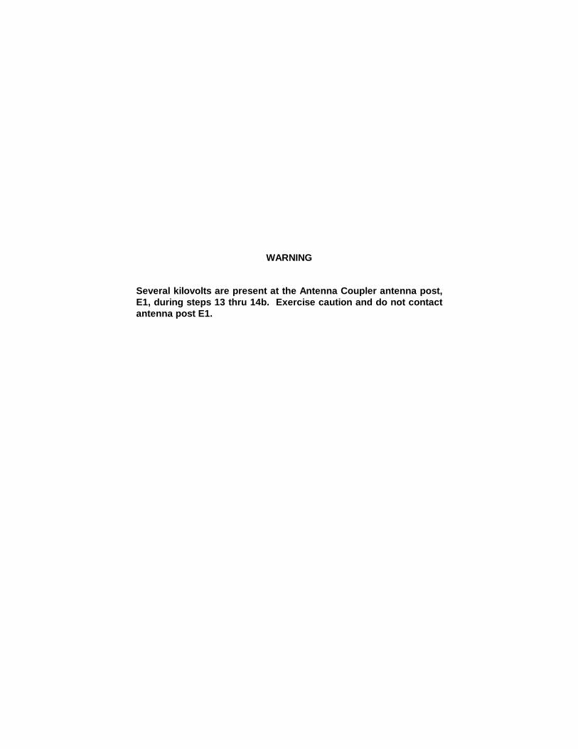
WARNING
Several kilovolts are present at the Antenna Coupler antenna post,E1, during steps 13 thru 14b. Exercise caution and do not contactantenna post E1.
TM 11-5820-873-34
TECHNICAL MANUAL HEADQUARTERSDEPARTMENT OF THE ARMY
No. 11-5820-873-34 WASHINGTON, DC 1 February 1980
Direct and General Support Maintenance ManualRADIO SET AN/URC-92(NSN 5820-01-057-6447)
REPORTING OF ERRORSYou can improve this manual by recommending improvements using DA Form 2028-2
(Test) located in the back of the manual. Simply tear out the self-addressed form, fill it out asshown on the sample, fold it where shown, and drop it in the mail.
If there are no blank DA Form 2028-2 (Test) in the back of your manual, use the standard DAForm 2028 (Recommended Changes to Publications and Blank Forms) and forward it toCommander, US Army Communications and Electronics Materiel Readiness Command, ATTN:DRSEL-ME-MQ Fort Monmouth, NJ 07703. A reply will be furnished direct to you.
Table of ContentsPara-graph Page
CHAPTER 1. INTRODUCTIONSection I. General ............................................................................................................................. 1-1 1-1
II. Description and data ......................................................................................................... 1-8 1-1CHAPTER 2. FUNCTIONING OF EQUIPMENTSection I. General ............................................................................................................................. 2-1 2-1
II. Radio receiver-transmitter RT-1277/URC-92 functional operation ...................................... 2-3 2-1III. Antenna coupler CU-2229/URC-92 functional operation................................................... 2-12 2-15
CHAPTER 3. DIRECT SUPPORTSection I. General ............................................................................................................................. 3-1 3-1
II. Tools and equipment......................................................................................................... 3-3 3-1III. Checkout/ troubleshoot...................................................................................................... 3-4 3-1IV Maintenance...................................................................................................................... 3-7 3-16V. Administrative Storage .................................................................................................... 3-13 3-18
CHAPTER 4. GENERAL SUPPORTSection I. General ............................................................................................................................. 4-1 4-1
II. Tools and equipment......................................................................................................... 4-3 4-1III. Checkout/troubleshoot....................................................................................................... 4-4 4-1IV. Maintenance...................................................................................................................... 4-7 4-32V. Administrative Storage .................................................................................................... 4-23 4-46
APPENDIX A. REFERENCES A-1INDEX Index 1
TABLE OF CONTENTSFigure Title Page1-1 Radio Set AN/URC-92 ...................................................................................................................... 1-21-2 Typical Warranty Notice ................................................................................................................... 1-32-1 Radio Receiver-Transmitter Simplified Block Diagram ...................................................................... 2-22-2 Power Supply Block Diagram............................................................................................................ 2-82-3 Synthesizer Simplified Block Diagram............................................................................................... 2-92-4 Antenna Coupler Control Unit Schematic Diagram............................................................................ 2-163-1 BNC/Chip Lead Cable....................................................................................................................... 3-13-2 Direct Support Checkout/Troubleshoot the Receiver-Transmitter Waveforms .................................... 3-53-3 Front Panel and Circuit Card Assemblies.......................................................................................... 3-173-4 Antenna Coupler Control................................................................................................................... 3-184-1 BNC/Chip Lead Cable....................................................................................................................... 4-14-2 General Support Checkout/Troubleshoot the Receiver-Transmitter Waveforms ................................. 4-54-3 Power Supply ................................................................................................................................... 4-344-4 Filter Module..................................................................................................................................... 4-364-5 Filter Module Circuit Cards ............................................................................................................... 4-374-6 Display Assembly ............................................................................................................................. 4-384-7 21 MHz Adjustment Setup (1A4A1)................................................................................................... 4-39
}
i
TM 11-5820-873-34
Figure Title Page4-8 17 MHz Adjustment Setup(1A4A1).................................................................................................... 4-394-9 19.45 MHz Adjustment Setup #1 (1A4A3) ......................................................................................... 4-404-10 19.45 MHz Adjustment Setup #2 (1A4A3) ......................................................................................... 4-404-11 19.45 MHz Adjustment Setup #3 (1A4A3) ......................................................................................... 4-414-12 100.75 MHz Bandpass Filter Adjustment Setup #1............................................................................ 4-414-13 100.75 MHz Bandpass Filter Adjustment Setup #2............................................................................ 4-414-14 100.75 MHz Bandpass Filter Adjustment Setup #3............................................................................ 4-414-15 81.25 MHz Bandpass Filter Adjustment Setup #1.............................................................................. 4-424-16 81.25 MHz Bandpass Filter Adjustment Setup #2.............................................................................. 4-424-17 VHF VCO CCA Adjustment Points .................................................................................................... 4-434-18 C MAX/C MIN Adjustment Locator .................................................................................................... 4-454-19 L MAX/L MIN Adjustment Locator ..................................................................................................... 4-454-20 Connection and Adjustment Points - Amplitude Detector Adjustment ................................................ 4-474-21 Connection and Adjustment Points - Phase Detector Adjustment ...................................................... 4-484-22 Back-Panel-Exploded View ............................................................................................................... 4-494-23 Receiver-Transmitter-Center............................................................................................................. 4-504-24 Spectrum Generator Circuit Card Assembly (CCA) ........................................................................... 4-514-25 Low Digit Generator (CCA) ............................................................................................................... 4-524-26 Translator(CCA) ............................................................................................................................... 4-534-27 VHF Divider(CCA) ............................................................................................................................ 4-544-28 VHF VCO(CCA)................................................................................................................................ 4-554-29 VHF Mixer(CCA)............................................................................................................................... 4-564-30 IF Filter (CCA) .................................................................................................................................. 4-574-31 Sideband Generator (CCA) ............................................................................................................... 4-584-32 Audio (CCA) ..................................................................................................................................... 4-594-33 Power Supply-Exploded View............................................................................................................ 4-604-34 Power Supply Chassis-Exploded View .............................................................................................. 4-614-35 Regulator Assy ................................................................................................................................. 4-624-36 Synthesizer Mother Board................................................................................................................. 4-634-37 Receiver/Exciter Mother Board.......................................................................................................... 4-644-38 DC Inverter-Exploded View ............................................................................................................... 4-654-39 DC Inverter (CCA) ............................................................................................................................ 4-664-40 RF Power Amplifier(CCA) ................................................................................................................. 4-674-41 Main Harness ................................................................................................................................... 4-684-42 Odd Channel Filter (CCA)................................................................................................................. 4-694-43 Even Channel Filter (CCA)................................................................................................................ 4-704-44 Receiver Filter (CCA)........................................................................................................................ 4-714-45 Motor Central Board Assembly ......................................................................................................... 4-724-46 Motor Central Board (CCA)............................................................................................................... 4-734-47 Front Panel Assembly (1 of 3)........................................................................................................... 4-744-47 Front Panel Assembly (2 of 3)........................................................................................................... 4-754-47 Front Panel Assembly (3 of 3)........................................................................................................... 4-764-48 Main Harness-Front Panel A Transmit B Receive Relay .................................................................... 4-774-49 Speaker Driver(CCA) ........................................................................................................................ 4-784-50 Decoder (CCA) ................................................................................................................................. 4-794-51 Display Assembly & (CCA) ............................................................................................................... 4-804-52 Tuning Control.................................................................................................................................. 4-814-53 Coupler Unit CU-2229/URC View B................................................................................................... 4-824-54 Coupler Unit CU-2229/URC View C .................................................................................................. 4-834-55 Main Harness ................................................................................................................................... 4-844-56 K2-K3 Relay Assembly ..................................................................................................................... 4-854-57 Control Logic (CCA) ......................................................................................................................... 4-864-58 Phase and Amplitude Control (CCA)................................................................................................. 4-874-59 Regulator (CCA) ............................................................................................................................... 4-884-60 Phase and Amplitude Assembly........................................................................................................ 4-894-61 Phase and Amplitude (CCA) ............................................................................................................. 4-904-62 Relay Control Assembly.................................................................................................................... 4-914-63 Servo Control (CCA)......................................................................................................................... 4-924-64 PCB Filter (CCA) .............................................................................................................................. 4-934-65 Rear Panel-Exploded View................................................................................................................ 4-944-66 Electrical Equipment Mounting Base MT-4982/URC-92..................................................................... 4-95
ii
TM 11-5820-873-34
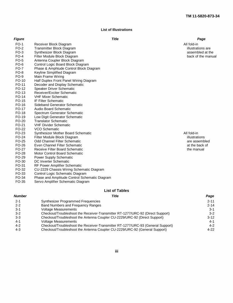
List of Illustrations
Figure Title PageFO-1 Receiver Block Diagram All fold-inFO-2 Transmitter Block Diagram illustrations areFO-3 Synthesizer Block Diagram assembled at theFO-4 Filter Module Block Diagram back of the manualFO-5 Antenna Coupler Block DiagramFO-6 Control Logic Board Block DiagramFO-7 Phase & Amphtude Control Block DiagramFO-8 Keyline Simplified DiagramFO-9 Main Frame WiringFO-10 Half Duplex Front Panel Wiring DiagramFO-11 Decoder and Display SchematicFO-12 Speaker Driver SchematicFO-13 Receiver/Exciter SchematicFO-14 VHF Mixer SchematicFO-15 IF Filter SchematicFO-16 Sideband Generator SchematicFO-17 Audio Board SchematicFO-18 Spectrum Generator SchematicFO-19 Low Digit Generator SchematicFO-20 Translator SchematicFO-21 VHF Divider SchematicFO-22 VCO SchematicFO-23 Synthesizer Mother Board Schematic All fold-inFO-24 Filter Module Block Diagram illustrationsFO-25 Odd Channel Filter Schematic are assembledFO-26 Even Channel Filter Schematic at the back ofFO-27 Receive Filter Board Schematic the manualFO-28 Motor Control Board SchematicFO-29 Power Supply SchematicFO-30 DC Inverter SchematicFO-31 RF Power Amplifier SchematicFO-32 CU-2229 Chassis Wiring Schematic DiagramFO-33 Control Logic Schematic DiagramFO-34 Phase and Amplitude Control Schematic DiagramFO-35 Servo Amplifier Schematic Diagram
List of TablesNumber Title Page2-1 Synthesizer Programmed Frequencies 2-112-2 Band Numbers and Frequency Ranges 2-143-1 Voltage Measurements 3-13-2 Checkout/Troubleshoot the Receiver-Transmitter RT-1277/URC-92 (Direct Support) 3-23-3 Checkout/Troubleshoot the Antenna Coupler CU-2229/URC-92 (Direct Support) 3-124-1 Voltage Measurements 4-14-2 Checkout/Troubleshoot the Receiver-Transmitter RT-1277/URC-93 (General Support) 4-24-3 Checkout/Troubleshoot the Antenna Coupler CU-2229/URC-92 (General Support) 4-22
iii
TM 11-5820-873-34
CHAPTER 1
INTRODUCTION
Section I. GENERAL
THE RADIO SET AN/URC-92 is COVERED BY A RELIABILITY IMPROVEMENT WARRANTY DONOT PERFORM ANY MAINTENANCE ON THIS EQUIPMENT UNTIL AFTER THE WARRANTYPROVISIONS (TM11-5820-873-12) HAVE BEEN COMPLIED WITH.
1-1. Scope.a. This manual contains direct and general support
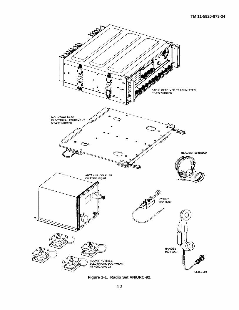
instructions for Radio Set AN/URC-92 (Fig. 1-1).Instructions for troubleshooting, testing, disassembling,inspecting, aligning and reassembling the componentsof the radio set are included in this manual. A detailedfunctional analysis of the AN/URC-92 is included inChapter 2.
b. The AN/URC-92 is comprised of Radio Receiver-Transmitter RT-1277/URC-92 and Antenna Coupler CU-2229/URC-92.
1-2. Forms and Records.a. Reports of Maintenance and Unsatisfactory
Equipment. Maintenance forms, records, and reportswhich are to be used by maintenance personnel at allmaintenance levels are listed in and prescribed by TM38-750, the Army Maintenance Management System.
b. Report of Packaging and Handling Deficiencies.Fill out and forward DD Form 6 (PackagingImprovement Report) as prescribed in AR 700-58/NAVSUPINST 4030 29/AFR 71-13/MCO P4030 29A,and DSAR 4145.8.
c. Discrepancy in Shipment Report (DISREP) (SF361). Fill out and forward Discrepancy in ShipmentReport (DISREP) (SF 361) as prescribed in AR 55-38/NAVSUPINST 4610 33B/AFR 75-18/MCO P461019C, and DLAR 4500.15.
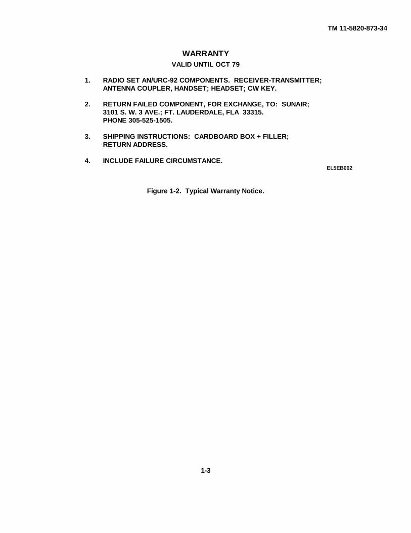
1-3. Warranty.a. This equipment is under a Reliability
Improvement Warranty. To ensure validation of thewarranty, the following steps must be taken whenreturning discrepant equipment.
(1) DA Form 2407 is to accompany the
equipment to the contractor's facility.(2) Fill in the required information on the
WARRANTY NOTICE attached to the equipment.b. Failure to provide the information required by
those documents may invalidate the warranty.c. Return the equipment as expeditiously as
possible to the contractor at the address shown on theWARRANTY NOTICE (figure 1-2).
1-4. Destruction of Army Materiel.Demolition and destruction of electronic equipment willbe under the direction of the commander and inaccordance with TM 750-4244-2.
1-5. Administrative Storage.Administrative storage of equipment issued to and usedby Army activities shall be in accordance with theprocedures specified. Refer to TM 11-5820-873-12 forspecific procedures to be followed when preparing theAN/URC-92 for administrative storage.
1-6. Calibration.Calibration is not required for Radio Set AN/URC-92.
1-7. Reporting Equipment ImprovementRecommendations (EIR).
If your Radio Set AN/URC-92 needs improvement, letus know. Send us an EIR. You, the user, are the onlyone who can tell us what you don't like about yourequipment. Let us know why you don't like the design.Tell us why a procedure is hard to perform. Put it on anSF 368 (Quality Deficiency Report). Mail it toCommander, US Army Communications and ElectronicsMateriel Readiness Command, ATTN: DRSEL-ME-MQ,Fort Monmouth, NJ 07703. We'll send you a reply.
Section II. Description of Radio Set
1-8. Description of Radio Set.Refer to TM 11-5820-873-12 for the description andillustrations of the components of Radio Set AN/URC-92.
1-9. Tabulated Data.Technical characteristics of Radio Set AN/URC-92 arelisted in TM 11-5820-873-12.
1-1
TM 11-5820-873-34
Figure 1-1. Radio Set AN/URC-92.
1-2
TM 11-5820-873-34
WARRANTYVALID UNTIL OCT 79
1. RADIO SET AN/URC-92 COMPONENTS. RECEIVER-TRANSMITTER;ANTENNA COUPLER, HANDSET; HEADSET; CW KEY.
2. RETURN FAILED COMPONENT, FOR EXCHANGE, TO: SUNAIR;3101 S. W. 3 AVE.; FT. LAUDERDALE, FLA 33315.PHONE 305-525-1505.
3. SHIPPING INSTRUCTIONS: CARDBOARD BOX + FILLER;RETURN ADDRESS.
4. INCLUDE FAILURE CIRCUMSTANCE.EL5EB002
Figure 1-2. Typical Warranty Notice.
1-3
TM 11-5820-873-34
CHAPTER 2
FUNCTIONING OF EQUIPMENT
Section I. GENERAL
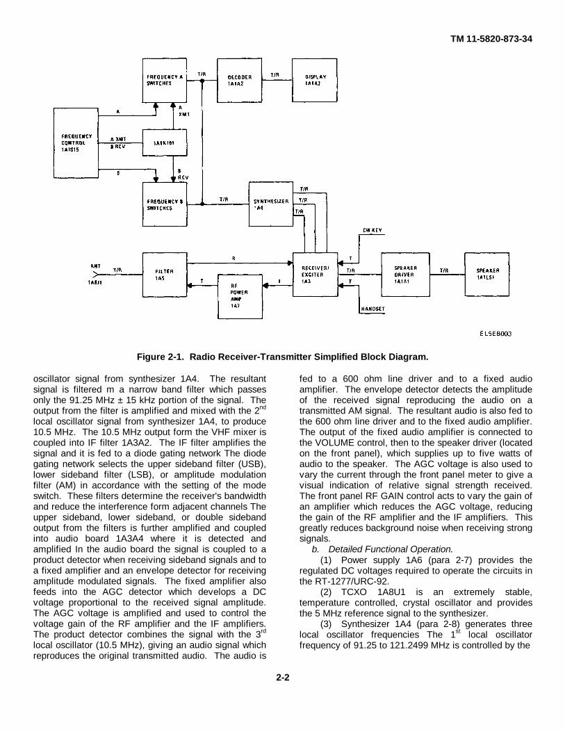
2-1. Introduction.This chapter describes how the radio set operates. Thechapter is divided into four sections which present theinformation in a logical sequence.
2-2. Description of Sections.a. Functional Operation of Radio Receiver-
Transmitter RT-1277/URC-92. Section II describes thefunctional operation of the RT-1277/URC-92. Thesection progresses from a simplified system explanationand block diagram to detailed circuit descriptions andblock diagrams. This presentation enables easyidentification of circuitry common in both receive andtransmit functions and that circuitry specific to eitherreceive or transmit.
NOTEAlthough ANTENNA COUPLERCONTROL 1A2 is housed in the radioset, it functions as part of the CU-2229/URC-92. Certain functioning withmeter 1A2M1 will be discussed in thissection but the remainder of ANTENNACOUPLER CONTROL 1A2 functions willbe covered in Section III.
b. Functional Operation of Antenna Coupler CU-2229/URC-92. Section III describes the functionaloperation CU-2229/URC-92.
c. Functional Operation of Circuits. Section IVdescribes the functional operation of non-conventionalcircuits and certain conventional circuits. Theconventional circuits discussed in this section are thosecircuits that perform functions that may not be readilyapparent to an experienced maintenance technician.
Section II. RADIO RECEIVER-TRANSMITTER RT-1277/URC-92 FUNCTIONAL OPERATION
2-3. Simplified Overall Operation (Fig. 2-1).a. Operating Frequency. The RT-1227/URC-92
operates over a frequency range of 1.6 to 29 9999 MHz.The operating frequency is determined by the setting ofFREQ CONTROL 1A1S15 and the FREQUENCY A andFREQUENCY B front panel switches.
(1) FREQ CONTROL 1A1S15 selects whichgroup of FREQUENCY switches that control theoperating frequency
(2) The setting of the selected FREQUENCYswitches is decoded by decoder 1A1A2 and displayedby LED display 1A1A3.
(3) Synthesizer 1A4 has three output frequencies.Two of the output frequencies are fixed and the thirdcontrols the operating frequency of the RT-1277/URC-92.
b. Receive Operation. The RF signal is received atANT jack 1A8J1 and passed through filter 1A5 toreceiver/exciter 1A3. The receiver/exciter converts theRF signal to audio. The audio signal is amplified byspeaker driver 1A1A1 and used to drive speaker1A1LS1.
c. Transmit Operation.(1) CW. Operating the CW Key causes a
sidetone to be generated in receiver/exciter 1A3. Thesidetone is coupled through speaker driver 1A1A1 tospeaker 1A1LS1. The receiver/exciter also uses thesidetone to modulate the signals from the synthesizer.The RF output from the receiver/exciter is amplified byRF power amplifier 1A7. The output from the RF poweramplifier is passed through filter 1A5 to ANT jack1A8J1.
(2) Voice Audio from the handset is coupled intoreceiver/exciter 1A3. The receiver/exciter uses theaudio to modulate the signals from the synthesizer. TheRF output from the receiver/exciter is amplified by RFpower amplifier 1A7. The output from the RF poweramplifier is passed through filter 1A5 to ANT jack1A8J1.
2-4. Receiver Functional Operation (Fig. FO-1).a. Overall Functional Operation. Incoming RF is
filtered by the selected bandpass filters in filter module1A5 (para 2-10). The output of the bandpass filters is anarrow segment of the RF spectrum that includes thefrequency selected by the FREQUENCY switches. Theoutput from the filter module is coupled into VHF mixer1A3A1 where it is fed through a high pass filter. Thesignal is then amplified and mixed with the 1st local
2-1
TM 11-5820-873-34
Figure 2-1. Radio Receiver-Transmitter Simplified Block Diagram.
oscillator signal from synthesizer 1A4. The resultantsignal is filtered m a narrow band filter which passesonly the 91.25 MHz ± 15 kHz portion of the signal. Theoutput from the filter is amplified and mixed with the 2nd
local oscillator signal from synthesizer 1A4, to produce10.5 MHz. The 10.5 MHz output form the VHF mixer iscoupled into IF filter 1A3A2. The IF filter amplifies thesignal and it is fed to a diode gating network The diodegating network selects the upper sideband filter (USB),lower sideband filter (LSB), or amplitude modulationfilter (AM) in accordance with the setting of the modeswitch. These filters determine the receiver's bandwidthand reduce the interference form adjacent channels Theupper sideband, lower sideband, or double sidebandoutput from the filters is further amplified and coupledinto audio board 1A3A4 where it is detected andamplified In the audio board the signal is coupled to aproduct detector when receiving sideband signals and toa fixed amplifier and an envelope detector for receivingamplitude modulated signals. The fixed amplifier alsofeeds into the AGC detector which develops a DCvoltage proportional to the received signal amplitude.The AGC voltage is amplified and used to control thevoltage gain of the RF amplifier and the IF amplifiers.The product detector combines the signal with the 3rd
local oscillator (10.5 MHz), giving an audio signal whichreproduces the original transmitted audio. The audio is
fed to a 600 ohm line driver and to a fixed audioamplifier. The envelope detector detects the amplitudeof the received signal reproducing the audio on atransmitted AM signal. The resultant audio is also fed tothe 600 ohm line driver and to the fixed audio amplifier.The output of the fixed audio amplifier is connected tothe VOLUME control, then to the speaker driver (locatedon the front panel), which supplies up to five watts ofaudio to the speaker. The AGC voltage is also used tovary the current through the front panel meter to give avisual indication of relative signal strength received.The front panel RF GAIN control acts to vary the gain ofan amplifier which reduces the AGC voltage, reducingthe gain of the RF amplifier and the IF amplifiers. Thisgreatly reduces background noise when receiving strongsignals.
b. Detailed Functional Operation.(1) Power supply 1A6 (para 2-7) provides the
regulated DC voltages required to operate the circuits inthe RT-1277/URC-92.
(2) TCXO 1A8U1 is an extremely stable,temperature controlled, crystal oscillator and providesthe 5 MHz reference signal to the synthesizer.
(3) Synthesizer 1A4 (para 2-8) generates threelocal oscillator frequencies The 1st local oscillatorfrequency of 91.25 to 121.2499 MHz is controlled by the
2-2
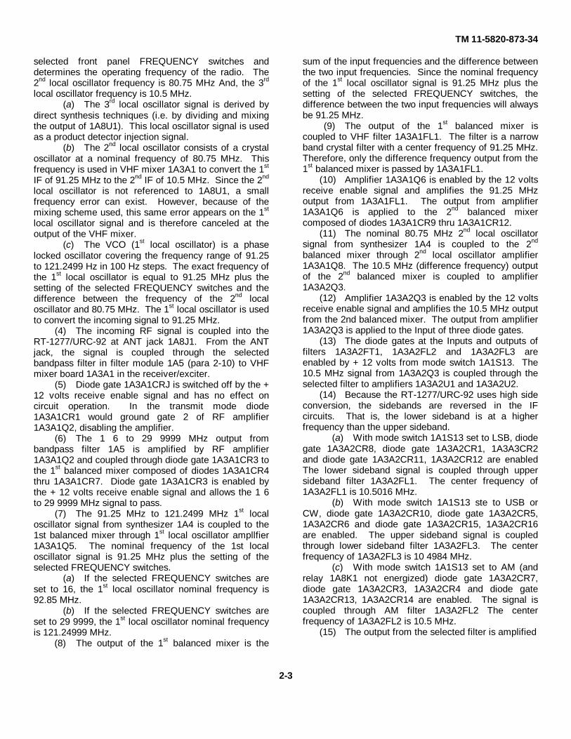
TM 11-5820-873-34
selected front panel FREQUENCY switches anddetermines the operating frequency of the radio. The2nd local oscillator frequency is 80.75 MHz And, the 3rd
local oscillator frequency is 10.5 MHz.(a) The 3rd local oscillator signal is derived by
direct synthesis techniques (i.e. by dividing and mixingthe output of 1A8U1). This local oscillator signal is usedas a product detector injection signal.
(b) The 2nd local oscillator consists of a crystaloscillator at a nominal frequency of 80.75 MHz. Thisfrequency is used in VHF mixer 1A3A1 to convert the 1st
IF of 91.25 MHz to the 2nd IF of 10.5 MHz. Since the 2nd
local oscillator is not referenced to 1A8U1, a smallfrequency error can exist. However, because of themixing scheme used, this same error appears on the 1st
local oscillator signal and is therefore canceled at theoutput of the VHF mixer.
(c) The VCO (1st local oscillator) is a phaselocked oscillator covering the frequency range of 91.25to 121.2499 Hz in 100 Hz steps. The exact frequency ofthe 1st local oscillator is equal to 91.25 MHz plus thesetting of the selected FREQUENCY switches and thedifference between the frequency of the 2nd localoscillator and 80.75 MHz. The 1st local oscillator is usedto convert the incoming signal to 91.25 MHz.
(4) The incoming RF signal is coupled into theRT-1277/URC-92 at ANT jack 1A8J1. From the ANTjack, the signal is coupled through the selectedbandpass filter in filter module 1A5 (para 2-10) to VHFmixer board 1A3A1 in the receiver/exciter.
(5) Diode gate 1A3A1CRJ is switched off by the +12 volts receive enable signal and has no effect oncircuit operation. In the transmit mode diode1A3A1CR1 would ground gate 2 of RF amplifier1A3A1Q2, disabling the amplifier.
(6) The 1 6 to 29 9999 MHz output frombandpass filter 1A5 is amplified by RF amplifier1A3A1Q2 and coupled through diode gate 1A3A1CR3 tothe 1st balanced mixer composed of diodes 1A3A1CR4thru 1A3A1CR7. Diode gate 1A3A1CR3 is enabled bythe + 12 volts receive enable signal and allows the 1 6to 29 9999 MHz signal to pass.
(7) The 91.25 MHz to 121.2499 MHz 1st localoscillator signal from synthesizer 1A4 is coupled to the1st balanced mixer through 1st local oscillator ampllfier1A3A1Q5. The nominal frequency of the 1st localoscillator signal is 91.25 MHz plus the setting of theselected FREQUENCY switches.
(a) If the selected FREQUENCY switches areset to 16, the 1st local oscillator nominal frequency is92.85 MHz.
(b) If the selected FREQUENCY switches areset to 29 9999, the 1st local oscillator nominal frequencyis 121.24999 MHz.
(8) The output of the 1st balanced mixer is the
sum of the input frequencies and the difference betweenthe two input frequencies. Since the nominal frequencyof the 1st local oscillator signal is 91.25 MHz plus thesetting of the selected FREQUENCY switches, thedifference between the two input frequencies will alwaysbe 91.25 MHz.
(9) The output of the 1st balanced mixer iscoupled to VHF filter 1A3A1FL1. The filter is a narrowband crystal filter with a center frequency of 91.25 MHz.Therefore, only the difference frequency output from the1st balanced mixer is passed by 1A3A1FL1.
(10) Amplifier 1A3A1Q6 is enabled by the 12 voltsreceive enable signal and amplifies the 91.25 MHzoutput from 1A3A1FL1. The output from amplifier1A3A1Q6 is applied to the 2nd balanced mixercomposed of diodes 1A3A1CR9 thru 1A3A1CR12.
(11) The nominal 80.75 MHz 2nd local oscillatorsignal from synthesizer 1A4 is coupled to the 2nd
balanced mixer through 2nd local oscillator amplifier1A3A1Q8. The 10.5 MHz (difference frequency) outputof the 2nd balanced mixer is coupled to amplifier1A3A2Q3.
(12) Amplifier 1A3A2Q3 is enabled by the 12 voltsreceive enable signal and amplifies the 10.5 MHz outputfrom the 2nd balanced mixer. The output from amplifier1A3A2Q3 is applied to the Input of three diode gates.
(13) The diode gates at the Inputs and outputs offilters 1A3A2FT1, 1A3A2FL2 and 1A3A2FL3 areenabled by + 12 volts from mode switch 1A1S13. The10.5 MHz signal from 1A3A2Q3 is coupled through theselected filter to amplifiers 1A3A2U1 and 1A3A2U2.
(14) Because the RT-1277/URC-92 uses high sideconversion, the sidebands are reversed in the IFcircuits. That is, the lower sideband is at a higherfrequency than the upper sideband.
(a) With mode switch 1A1S13 set to LSB, diodegate 1A3A2CR8, diode gate 1A3A2CR1, 1A3A3CR2and diode gate 1A3A2CR11, 1A3A2CR12 are enabledThe lower sideband signal is coupled through uppersideband filter 1A3A2FL1. The center frequency of1A3A2FL1 is 10.5016 MHz.
(b) With mode switch 1A1S13 ste to USB orCW, diode gate 1A3A2CR10, diode gate 1A3A2CR5,1A3A2CR6 and diode gate 1A3A2CR15, 1A3A2CR16are enabled. The upper sideband signal is coupledthrough lower sideband filter 1A3A2FL3. The centerfrequency of 1A3A2FL3 is 10 4984 MHz.
(c) With mode switch 1A1S13 set to AM (andrelay 1A8K1 not energized) diode gate 1A3A2CR7,diode gate 1A3A2CR3, 1A3A2CR4 and diode gate1A3A2CR13, 1A3A2CR14 are enabled. The signal iscoupled through AM filter 1A3A2FL2 The centerfrequency of 1A3A2FL2 is 10.5 MHz.
(15) The output from the selected filter is amplified
2-3
TM 11-5820-873-34
by amplifiers 1A3A2U1 and 1A3A2U2 and coupled tothe inputs of amplifier 1A3A4Q1 and product detector1A3A4Q6, 1A3A4Q8, 1A3A4Q9.
(a) The output from amplifier 1A3A4Q1 iscoupled to emitter follower 1A3A4Q2 and AM detector1A3A4Q7, 1A3A4Q10.
1. The output from emitter follower1A3A4Q2 is coupled to AGC detector 1A3A4Q3. TheDC output from 1A3A4Q3 is coupled to emitter follower1A3A4Q4. The output of 1A3A4Q4 is the AGC voltageRF gain control amplifier 1A3A4Q12 is connectedacross the AGC line, RF GAIN control 1A1R55 controlsthe gain of 1A3A4Q12 and established the minimumlevel of AGC. With 1A1R55 fully counterclockwise, itshould be possible to completely disable the receiver.The AGC voltage is also used to drive S meter amplifier1A3A4Q5. The output of 1A3A4Q5 drives meter1A2M1.
2. When extremely high signal levels arepresent, peak signal level AGC amplifier 1A3A5Q2limits the level of input signal that is applied to RFamplifier 1A3A1Q2.
3. With mode switch 1A1S13 set to AM(and relay 1A8K1 not energized) AM detector 1A3A4Q7,1A3A4Q10 is enabled. The 10.5 MHz signal from1A3A4Q1 is detected by AM detector 1A3A4Q7,1A3A4Q10. The audio signal from the AM detector iscoupled to the inputs of 600 ohm audio line driver1A3A4U1 and audio amplifier 1A3A4Q11.
(b) With mode switch 1A1S13 set to LSB, USBor CW product detector 1A3A4Q6, 1A3A4Q8, 1A3A4Q9is enabled. The 10.5 MHz 3rd local oscillator signalfrom the synthesizer is mixed with the 10.5 MHz signalfrom amplifier 1A3A2U1, 1A3A2U2 in product detector1A3A4Q6, 1A3A4Q8, 1A3A4Q9. The audio signal fromthe product detector is coupled to the inputs of 600 ohmaudio line driver 1A3A4U1 and audio amplifier1A3A4Q11.
(16) The audiot signal from 600 ohm audio linedriver 1A3A4U1 is coupled to AUDIO connector 1A8J2.The audio signal from audio amplifier 1A3A4Q11 iscoupled through VOLUME control 1A1R51 to speakerdriver 1A1A1. The output from 1A1A1 is coupledthrough the normally closed contacts of PHONE jack1A1J3 to speaker 1A1LS1.
2-5. Transmitter Functional Operation(Fig. FO-2).
The RT-1277/URC-92 can be used in the transmit modein any setting of the mode switch. This paragraphdescribes functional operation as a transmitter with themode switch set to LSB, USB, AM, or CW For functionaloperation with the mode switch set to CPLR TUNE KWrefer to paragraph 2-6.
a. Overall Functional Operation. The RT-1277/URC-92 is placed in the transmit mode by
operating the press-to-talk switch on the handset, bygrounding the keyline at AUDIO connector 1A8J2, or byoperating the CW key. Operating the CW key energizesthe CW tone oscillator, which produces a 1 kHz audiosignal. Input audio from the handset, the 600 ohmbalanced line, or the CW tone oscillator is amplified andused to modulate the 10.5 MHz, 3rd local oscillatorsignal from synthesizer 1A4. The resultant doublesideband suppressed carrier signal is amplified andfiltered in accordance with the setting of the modeswitch. The remaining upper or lower sideband signal(AM transmission is actually upper sideband pluscarrier) is amplified and, if the mode switch is set to AM,mixed with the 10.5 MHz carrier signal. The lowersideband, upper sideband, or upper sideband pluscarrier signal is mixed with the 80.75 MHz of the 2ndlocal oscillator signal from synthesizer 1A4. Theresultant signals are amplified and passed through a91.25 MHz (sum frequency) filter. The 91.25 MHzsignal is mixed with the 91.25 to 121.2499 MHz, 1stlocal oscillator signal, from synthesizer 1A4. Thedifference frequency (1st local oscillator frequencyminus 91.25 MHz) is amplified to the 100 watt level andpassed through a low pass filter to ANT jack 1A8J1.
b. Detailed Functional Operation.(1) Power supply 1A6 (para 2-7) provides the
regulated DC voltages required to operate the circuits inthe RT-1277/URC-92.
(2) TCXO 1A8U1 is an extremely stable,temperature controlled, crystal oscillator and providesthe 5 MHz reference signal to the synthesizer.
(3) Synthesizer 1A4 (para 2-8) generates threelocal oscillator frequencies. The 1st local oscillatorfrequency of 91.25 to 121.2499 MHz is controlled by theselected front panel FREQUENCY switches anddetermines the operating frequency of the radio. The2nd local oscillator frequency is 80.75 MHz. And, the3rd local oscillator frequency is 10.5 MHz.
(a) The 3rd local oscillator signal is derived bydirect synthesis techniques (i.e. by dividing and mixingthe output of 1A8U1). This local oscillator signal is usedas a carrier generator.
(b) The 2nd local oscillator consists of a crystaloscillator at a nominal frequency of 80.75 MHz. Thisfrequency is used in VHF mixer 1A3A1 to convert the1st IF of 91.25 MHz to the 2nd IF of 10.5 MHz. Sincethe 2nd local oscillator is not referenced to 1A8U1, asmall frequency error can exist. However, because ofthe mixing scheme used, this same error appears on the1st local oscillator signal and is therefore canceled atthe output of the VHF mixer.
(c) The VCO (1st local oscillator) is a phaselocked oscillator covering the frequency range of 91.25to 121.2499 Hz in 100 Hz steps. The exact frequency ofthe 1st local oscillator is equal to 91.25 MHz plus thesetting of the selected FREQUENCY switches and
2-4
TM 11-5820-873-34
the difference between the frequency of the 2nd localoscillator and 80.75 MHz. The 1st local oscillator isused to convert the 1st IF frequency of 91.25 MHz to theselected operating frequency.
(4) The RT-1277/URC-92 is normally in thereceive mode It is placed in the transmit mode whenrelays 1A5A4K2 and 1A8K1 are energized (see para 2-22 for a discussion of the keying circuits). The relaysare energized as follows:
(a) Operating the press-to-talk switch on thehandset energizes relays 1A5A4K2 and 1A8K1 whenmode switch 1A1S13 is set to LSB, USB, or AM.
(b) Grounding the keyline at AUDIO connector1A8J2 (600 ohm audio) energizes relays 1A5A4K2 and1A8K1 when mode switch 1A1S13 is set to LSB, USB,CW, or AM.
(c) Operating the CW key causes transistors1A3AQ12 and 1A3A3Q14 to energize relays 1A5A4K2and 1A8K1 when mode switch 1A3S13 is set to CW.Transistors 1A3A3Q12 and 1A3A3Q14 hold the relaysenergized for approximately 1 second after the CW keyis released. This prevents the relays from deenergizingbetween normal CW characters and words butautomatically returns the unit to the receive mode whenthe CW key has not been operated for 1 second. Thisdelay is adjusted by 1A3A3R50.
(5) Audio is brought into the RT-1277/URC-92 asfollows:
(a) Audio from the handset is coupled throughXMT GAIN control 1A1R58 to microphone audioamplifier 1A3A3Q4 when mode switch 1A1S13 is set toLSB, USB, or AM. The amplified audio from 1A3A3Q4is applied to balanced modulator 1A3A3CR3 thru1A3A3CR6.
(b) Audio from the 600 ohm balanced input isamplified by 600 ohm audio amplifier 1A3A3Q11. Theamplified audio from 1A3A3Q11 is applied to balancedmodulator 1A3A3CR3 thru 1A3A3CR6.
(c) Operating the CW key turns on the CW toneoscillator, 1A3A3Q7 and 1A3A3Q8, when mode switch1A1S13 is set to CW. The 1 kHz tone from the CWtone oscillator is applied to 600 ohm audio line driver1A3A4U1, audio amplifier 1A3A4Q11, and emitterfollower 1A3A3Q6.
1. The audio signal from 600 ohm audioline driver 1A3A4U1 is coupled to AUDIO connector1A8J2.
2. The audio signal from audio amplifier1A3A411 is coupled through VOLUME control 1A1R51to speaker driver 1A1A1. The output from 1A1A1 iscoupled through the normally closed contacts of PHONEjack 1A1J3 to speaker 1A1LSL.
3. The audio signal from emitter follower1A3A3Q6 is applied to balanced modulator 1A3A3CR3thru 1A3A3CR6.
(6) When the transmit enable signal is present
and the mode switch is not m CPLR TUNE KW, transmitaudio enable/disable switch 1A3A5Q1 is enabled. Thisenables 3rd local oscillator amplifier 1A3A3Q1. The10.5 MHz 3rd local oscillator signal from synthesizer1A4 is amplified by 3rd local oscillator amplifier1A3A3Q1 and applied to balanced modulator1A3A3CR3 thru 1A3A3CR6.
(7) The balanced modulator modulates the 10.5MHz 3rd local oscillator signal with the audio signal fromeither of the three audio sources ((5) above). Theoutput from the balanced modulator is a doublesideband suppressed carrier signal at 10.5 MHz. Thedouble sideband suppressed carrier signal from thebalanced modulator is applied to IF amplifier 1A3A2Q4.
(8) IF amplifier 1A3A2Q4 is enabled by thetransmit enable signal and amplifies the output from thebalanced modulator. The output from 1A3A2Q4 iscoupled to the inputs of two diode gates.
(9) The diode gates at the inputs and outputs offilters 1A3A2FL1 and 1A3A2FL2 are enabled by + 12volts from mode switch 1A1S13. The 10.5 MHz signalis coupled through the selected filter to amplifier1A3A2Q1, 1A3A2Q2.
(10) Because the RT-1277/URC-92 uses high sideconversion, the sidebands are reversed in the IFcircuits. That is, the lower sideband is at a higherfrequency than the upper sideband.
(a) With mode switch 1A1S13 set to LSB, diodegate 1A3A2CR8, diode gate 1A3A2CR1, 1A3A2CR2and diode gate 1A3A2CR11, 1A3A2CR12 are enabled.The lower sideband signal is coupled through uppersideband filter 1A3A2FL1. The center frequency of1A3A2FL1 is 10.5016 MHz.
(b) With mode switch 1A1S13 set to USB orCW, diode gate 1A3A2CR10, diode gate 1A3A2CR5,1A3A2CR6 and diode gate 1A3A2CR15, 1A3A2CR16are enabled. The upper sideband signal is coupledthrough lower sideband filter 1A3A2FL3. The centerfrequency of 1A3A2FL3 is 10.4984 MHz.
(c) The AM transmit mode of the RT-1277/URC-92 is actually upper sideband plus carrier.With mode switch 1A1S13 set to AM and relay 1A8K1energized, diode gate 1A3A2CR9, diode gate1A3A2CR5, 1A3A2CR6 and diode gate 1A3A2CR15,1A3A2CR16 are enabled. The upper sideband signal iscoupled through lower sideband filter 1A3A2FL3. Theupper sideband signal is combined with the 10.5 MHzcarrier signal by amplifier 1A3A2Q1, 1A3A2Q2 ((12)below).
(11) The gain of amplifier 1A3A2Q1, 1A3A2Q2 iscontrolled by the output of ALC amplifier 1A3A3Q9,1A3A3Q10 ((19) below). The ALC voltage limits thegain of 1A3A2Q1, 1A3A2Q2 when the transmitter outputreaches 100 watts peak or there is a higher VSWR atthe transmitter output. Amplifier 1A3A2Q1, 1A3A2Q2 isenabled by the transmit enable signal and amplifies the
2-5
TM 11-5820-873-34
signal from the selected filter when mode switch1A1S13 is set to LSB, USB or CW The output from theamplifier is coupled to 2nd balanced mixer 1A3A1CR9thru 1A3A1CR12.
(12) When mode switch 1A1S13 is set to AM,amplifier 1A3A2Q1, 1A3A2Q2 combines the uppersideband signal with the 10.5 MHz carrier signal andamplifies the combined signal ((11) above).
(a) The AM/CPLR TUNE KW transmit enablesignal is coupled from mode switch 1A1S13 throughrelay 1A8K1 to turn on AM transmit switch 1A3A3Q13.The AM transmit switch enables automatic carriercontrol (ACC) amplifier 1A3A3Q2, 1A3A3Q3, 1A3A3Q5.
(b) The gain of the automatic carrier controlamplifier is controlled by the detected carrier signal fromACC detector 1A5A4CR6, 1A5A4CR12 ((20) below).The automatic carrier control amplifier amplifies the10.5 MHz 3rd local oscillator signal. The amplified 3rdlocal oscillator signal is injected into amplifier 1A3A2Q1,1A3A2Q2 where it is combined with the upper sidebandsignal.
(13) The nominal 80.75 MHz 2nd local oscillatorsignal from synthesizer 1A4 is coupled to the 2ndbalanced mixer through 2nd local oscillator amplifier1A3A1Q8. The output from the 2nd balanced mixer iscoupled to amplifier 1A3A1Q7.
(14) Amplifier 1A3A1Q7 is enabled by the transmitenable signal and amplifies the output from the 2ndbalanced mixer. The 91.25 MHz (sum frequency)output signal from lA3A1Q7 is coupled through VHFfilter 1A3A1FL1 to 1st balanced mixer 1A3A1CR4 thru1A3A1CR7.
(15) The 91.25 MHz to 121.2499 MHz 1st localoscillator signal from synthesizer 1A4 is coupled to the1st balanced mixer through 1st local oscillator amplifier1A3A1Q5. The nominal frequency of the 1st localoscillator signal is 91.25 MHz plus the setting of theselected FREQUENCY switches. If the selectedFREQUENCY switches are set to 12.3456, the 1st localoscillator frequency is 103.5956 MHz. The output of the1st balanced mixer is coupled to amplifier 1A3A1Q1,1A3A1Q3.
(16) The gain of amplifier 1A3A1Q1, 1A3A1Q3 iscontrolled by the output of current ALC amplifier1A3A1Q4 ((18) below). The current ALC amplifier limitsthe gain of 1A3A1Q1, 1A3A1Q3 during high currentpeaks. Amplifier 1A3A1Q1, 1A3A1Q3 is enabled by thetransmit enable signal and amplifies the differencefrequency (equal to the setting of the selectedFREQUENCY switches) output of the 1st balancedmixer.
(17) RF power amplifier 1A7A1Q11 thru 1A7A1Q6is enabled by the transmit enable signal and amplifiesthe HF signal from 1A3A1Q1, 1A3A1Q3 to the 100 wattlevel. The output from the RF power amplifier is
coupled through the selected low pass filter (para 2-10)to ANT jack 1A8J1.
(18) Current ALC detector 1A7A17 monitors thesupply current to the RF power amplifier. When thesupply current exceeds 10 amperes, 1A7A1Q7 is turnedon causing current ALC amplifier 1A3A1Q4 to reducethe gain of amplifier 1A3A1Q1l, 1A3A1Q3.
(19) ALC amplifier 1A3A3Q9, 1A3A3Q10 limits thegain of amplifier 1A3A2Q1, 1A3A2Q2 when the VSWRis too high or the RF output voltage is too high.
(a) VSWR ALC detector 1A7A1CR4 causes theALC amplifier to limit the gain of amplifier 1A3A2Q1,1A3A2Q2 when the peak voltage on the collector of1A7A1Q6 is too high.
(b) Reflected power detector 1A5A4CR16causes the ALC amplifier to limit the gain of amplifier1A3A2Q1, 1A3A2Q2 when the VSWR on the RF outputline is too high.
(c) Voltage ALC detector 1A5A4Q2, 1A5A4Q3causes the ALC amplifier to limit the gain of amplifier1A3A2Q1, 1A3A2Q2 when the RF output voltage is toohigh.
(20) ACC detector 1A5A4CR6, 1A5A4CR12reduces the gain of automatic carrier control amplifier1A3A3Q2, 1A3A3Q3, 1A3A3Q5. At initial turn on in AMtransmit mode, automatic carrier control amplifier1A3A3Q2, 1A3A3Q3, 1A3A3Q5 is operating atmaximum gain ACC detector 1A5A4CR6, 1A5A4CR12detects the level of carrier signal on the RF output lineand reduces the gain of the automatic carrier controlamplifier to establish the desired carrier signal level.
(21) Power output detector 1A5A4CR5 samplesthe voltage on the RF output line. The output from1A5A4CR5 drives meter 1A2M1 when FWD power isselected by 1A2S1.
2-6. CPLR TUNE KW Functional Operation(Fig. FO-2)
With mode switch 1A1S13 in CPLR TUNE KW, pressingTUNE START switch 1A2S2 places the RT-1277/URC-92 in the transmit mode. Relays 1A5A4K2 and 1A8K1are energized through the SU-2229/URC-92.
a. Overall Functional Operation. The 10.5 MHz, 3rdlocal oscillator signal from synthesizer 1A4 is amplifiedand mixed with the 80.75 MHz, 2nd local oscillatorsignal from synthesizer 1A4. The resultant signals areamplified and passed through a 91.25 MHz (sumfrequency) filter. The 91.25 MHz signal is mixed withthe 91.25 to 121.2499 MHz, 1st local oscillator signalfrom synthesizer 1A4. The difference frequency (1stlocal oscillator frequency minus 91.25 MHz) is amplifiedto the 30-40 watt level and passed through a low passfilter to ANT jack 1A8J1.
b. Detailed Functional Operation.
2-6
TM 11-5820-873-34
(1) Power supply 1A6 (para 2-7) provides theregulated DC voltages required to operate the circuits inthe RT-1277/URC-92.
(2) TCXO 1A8U1 is an extremely stable,temperature controlled, crystal oscillator and providesthe 5 MHz reference signal to the synthesizer.
(3) Synthesizer 1A4 (para 2-8) generates threelocal oscillator frequencies. The 1st local oscillatorfrequency of 91.25 to 121.2499 MHz is controlled by theselected front panel FREQUENCY switches anddetermines the operating frequency of the radio. The2nd local oscillator frequency is 80.75 MHz. And, the3rd local oscillator frequency is 10.5 MHz.
(a) The 3rd local oscillator signal is derived bydirect synthesis techniques (i.e. by dividing and mixingthe output of 1A8U1). This local oscillator signal is usedto generate the carrier signal.
(b) The 2nd local oscillator consists of a crystaloscillator at a nominal frequency of 80.75 MHz. Thisfrequency is used in VHF mixer 1A3A1 to convert the1st IF of 91.25 MHz to the 2nd IF of 10.5 MHz. Sincethe 2nd local oscillator is not referenced to 1A8U1, asmall frequency error can exist. However, because ofthe mixing scheme used, this same error appears on the1st local oscillator signal and is therefore canceled atthe output of the VHF mixer.
(c) The VCO (1st local oscillator) is a phaselocked oscillator covering the frequency range of 91.25to 121.2499 Hz in 100 Hz steps. The exact frequency ofthe 1st local oscillator is equal to 91.25 MHz plus thesetting of the selected FREQUENCY switches and thedifference between the frequency of the 2nd localoscillator and 80.75 MHz. The 1st local oscillator isused to convert the 1st IF frequency of to 91.25 MHz tothe selected operating frequency.
(4) Transmit audio enable/disable switch1A3A5Q1 is turned off by the audio disable from modeswitch 1A1S13. This blocks the transmit enable from1A8K1 and 3rd local oscillator amplifier 1A3A3Q1 is notenabled. With no 10.5 MHz input, balanced modulator1A3A3CR3 thru 1A3A3CR6 has no output and audio cannot enter the IF circuits.
(5) The AM/CPLR TUNE KW transmit enablesignal is coupled from mode switch 1A1S13 throughrelay 1A8K1 to turn on AM transmit switch 1A3A3Q13.The AM transmit switch enables automatic carriercontrol amplifier 1A3A3Q2, 1A3A3Q3, and 1A3A3Q5.The gain of the automatic carrier control amplifier isestablished by the setting of 1A3A3R18.
(6) The 10.5 MHz, 3rd local oscillator signal fromsynthesizer 1A4 is amplified by the automatic carriercontrol amplifier and coupled to the input of amplifier1A3A2Q1, 1A3A2Q2.
(7) Amplifier 1A3A2Q1, 1A3A2Q2 is enabled bythe transmit enable signal and amplifies the 10.5 MHzcarrier signal from the automatic carrier control
amplifier. The output from amplifier 1A3A2Q1,1A3A2Q2 is coupled to 2nd balanced mixer 1A3A1CR9thru 1A3A1CR12 ALC amplifier 1A3A3Q9, 1A3A3Q10has no effect on 1A3A2Q1, 1A3A2Q2. If no VSWR ALCsignal, PA high voltage or PA high current ALC inputvoltages are present at the inputs of 1A3A3Q9 &1A3A3Q10. The voltage ALC does not take effect untilthe transmitter output reaches 100 watt peak(transmitter output in CPLR TUNE KW mode is 30 to 40watts).
(8) The nominal 80.75 MHz, 2nd local oscillatorsignal from synthesizer 1A4 is coupled to the 2ndbalanced mixer through 2nd local oscillator amplifier1A3A1Q8. The output from the 2nd balanced mixer iscouple to amplifier 1A3A1Q7.
(9) Amplifier 1A3A1Q7 is enabled by the transmitenable signal and amplifies the output from the 2ndbalanced mixer. The 91.25 MHz (sum frequency)output signal from 1A3A1Q7 is coupled through VHFfilter 1A3A1FL1 to 1st balanced mixer 1A3A1CR4 thru1A3A1CR7.
(10) The 91.25 MHz to 121.2499 MHz, 1st localoscillator signal from synthesizer 1A4 is coupled to the1st balanced mixer through 1st local oscillator amplifier1A3A1Q5. The nominal frequency of the 1st localoscillator signal is 91.25 MHz plus the setting of theselected FREQUENCY switches. (If the selectedFREQUENCY switches are set to 12.3456, the 1st localoscillator frequency is 103.5956 MHz.) The output ofthe 1st balanced mixer is coupled to amplifier 1A3A1Q1,1A3A1Q3.
(11) The gain of amplifier 1A3A1Q1, 1A3A1Q3 iscontrolled by the output of current ALC amplifier1A3A1Q4 ((13) below). The current ALC amplifier limitsthe gain of 1A3A1Q1, 1A3A1Q3 during high currentpeaks. Amplifier 1A3A1Q1, 1A3A1Q3 is enabled by thetransmit enable signal and amplifies the differencefrequency (equal to the setting of the selectedFREQUENCY switches) output of the 1st balancedmixer.
(12) RF power amplifier 1A7A1Q1 thru 1A7A1Q6is enabled by the transmit enable signal and amplifiesthe HF signal from 1A3A1Q1, 1A3A1Q3 to the 100 wattlevel (30-40 watts AM & CPLR TUNE KW). The outputfrom the RF power amplifier is coupled through theselected low pass filter (para 2-10) to ANT jack 1A8J1.
(13) Current ALC detector 1A7A1Q7 monitors thesupply current to the RF power amplifier. When thesupply current exceeds 10 amperes, 1A7A1Q7 is turnedon causing current ALC amplifier 1A3A1Q4 to reducethe gain of amplifier 1A3A1Q11, 1A3A1Q3.
(14) Power output detector 1A5A4CR5 samplesthe voltage on the RF output line. The output from1A5A4CR5 drives meter 1A2M1 when FWD power isselected by 1A2S1.
2-7
TM 11-5820-873-34
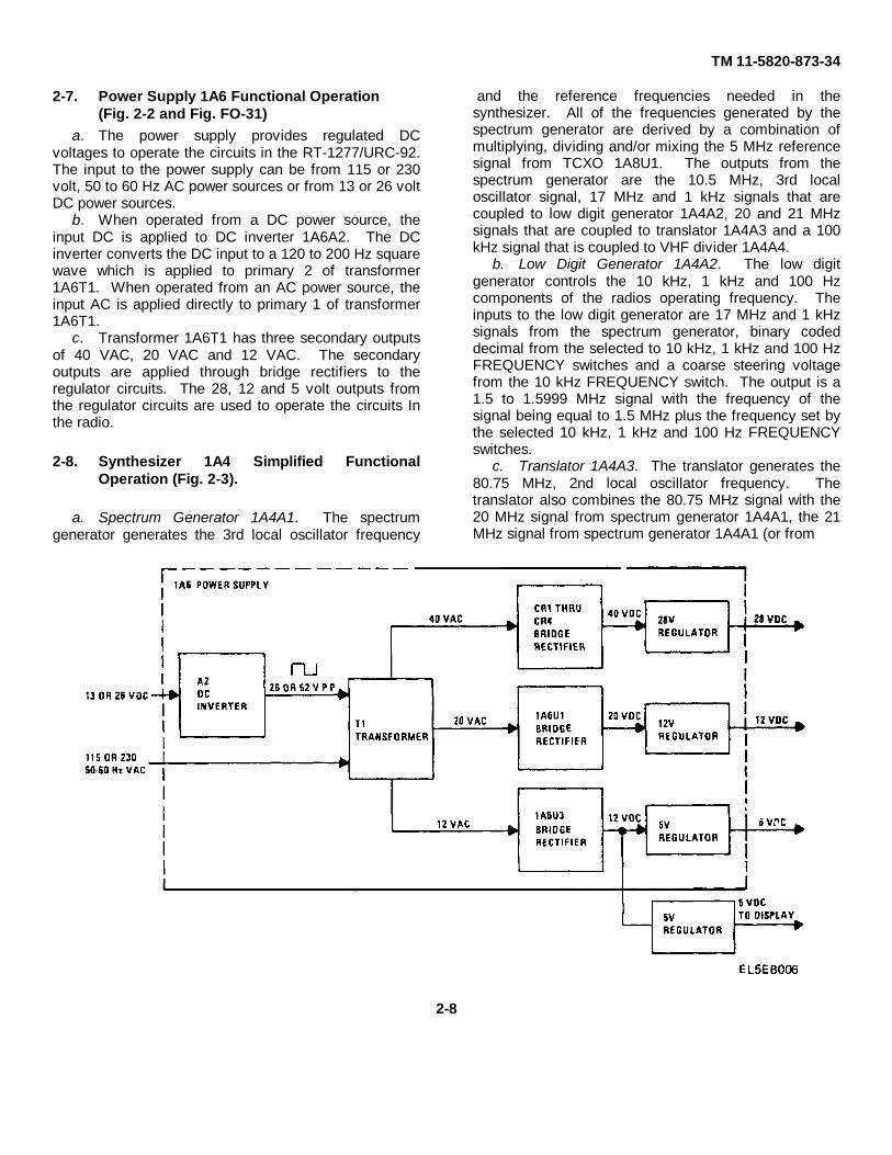
2-7. Power Supply 1A6 Functional Operation(Fig. 2-2 and Fig. FO-31)
a. The power supply provides regulated DCvoltages to operate the circuits in the RT-1277/URC-92.The input to the power supply can be from 115 or 230volt, 50 to 60 Hz AC power sources or from 13 or 26 voltDC power sources.
b. When operated from a DC power source, theinput DC is applied to DC inverter 1A6A2. The DCinverter converts the DC input to a 120 to 200 Hz squarewave which is applied to primary 2 of transformer1A6T1. When operated from an AC power source, theinput AC is applied directly to primary 1 of transformer1A6T1.
c. Transformer 1A6T1 has three secondary outputsof 40 VAC, 20 VAC and 12 VAC. The secondaryoutputs are applied through bridge rectifiers to theregulator circuits. The 28, 12 and 5 volt outputs fromthe regulator circuits are used to operate the circuits Inthe radio.
2-8. Synthesizer 1A4 Simplified FunctionalOperation (Fig. 2-3).
a. Spectrum Generator 1A4A1. The spectrumgenerator generates the 3rd local oscillator frequency
and the reference frequencies needed in thesynthesizer. All of the frequencies generated by thespectrum generator are derived by a combination ofmultiplying, dividing and/or mixing the 5 MHz referencesignal from TCXO 1A8U1. The outputs from thespectrum generator are the 10.5 MHz, 3rd localoscillator signal, 17 MHz and 1 kHz signals that arecoupled to low digit generator 1A4A2, 20 and 21 MHzsignals that are coupled to translator 1A4A3 and a 100kHz signal that is coupled to VHF divider 1A4A4.
b. Low Digit Generator 1A4A2. The low digitgenerator controls the 10 kHz, 1 kHz and 100 Hzcomponents of the radios operating frequency. Theinputs to the low digit generator are 17 MHz and 1 kHzsignals from the spectrum generator, binary codeddecimal from the selected to 10 kHz, 1 kHz and 100 HzFREQUENCY switches and a coarse steering voltagefrom the 10 kHz FREQUENCY switch. The output is a1.5 to 1.5999 MHz signal with the frequency of thesignal being equal to 1.5 MHz plus the frequency set bythe selected 10 kHz, 1 kHz and 100 Hz FREQUENCYswitches.
c. Translator 1A4A3. The translator generates the80.75 MHz, 2nd local oscillator frequency. Thetranslator also combines the 80.75 MHz signal with the20 MHz signal from spectrum generator 1A4A1, the 21MHz signal from spectrum generator 1A4A1 (or from
2-8
TM 11-5820-873-34
an internal oscillator with the VFO control on), the 1.5 to1.5999 MHz signal from low digit generator 1A4A2 andthe 91.25 to 121.2499 MHz signal from VCO 1A4A5,and produces a 10.0 to 39 9 MHz signal. The 10.0 to39.9 MHz signal is coupled to VHF divider 1A4A4. Thefrequency of the 1.5 to 1.5999 MHz signal is equal to 1 5MHz plus the frequency set by the selected 10 kHz, 1kHz and 100 Hz FREQUENCY switches. The frequencyof the 91.25 to 121.2499 MHz signal from VCO 1A4A5is equal to 91.25 MHz plus the frequency set by all ofthe selected FREQUENCY switches. The frequency ofthe 10.0 to 39 9 MHz signal is equal to 10.0 MHz plusthe setting of the selected 10 MHz, 1 MHz and 100 kHzFREQUENCY switches and the difference between thefrequency of the 2nd local oscillator and 80.75 MHz.
d. VHF Divider 1A4A4. The VHF divider generatesa fine steering control voltage for VCO 1A4A5. Theinputs to the VHF divider are a 100 kHz reference signalfrom spectrum generator 1A4A1, a 10.0 to 39 9 MHzsignal from translator 1A4A3, binary coded decimal fromthe selected 1 MHz and 100 kHz FREQUENCY switchesand binary coded decimal, representing the setting ofthe selected 10 MHz FREQUENCY switch, from VCO1A4A5. The VHF divider compares the input signalsand generates a fine steering correction voltage thatrepresents the difference between the frequency of the91.25 to 121.2499 MHz signal from VCO 1A4A5 and thefrequency set by the selected FREQUENCY switchesplus 91.25 MHz plus the difference between the
frequency of the 2nd local oscillator and 80.75 MHz.e. VCO 1A4A5. The voltage controlled oscillator
generates the 91.25 to 121.2499 MHz, 1st localoscillator frequency. The variable frequency 1st localoscillator signal controls the operating frequency of theRT-1277/URC-92. The output frequency from the VCOis equal to the frequency set by the selectedFREQUENCY switches plus 91.25 MHz and thedifference between the frequency of the 2nd localoscillator and 80.75 MHz The VCO frequency isdetermined by the following:
Fs - (FO + 91.25 MHz = e)where:
Fs = 91.25 to 121.2499 MHz signal from VCO1A4A5
Fo = Frequency set by selected FREQUENCYswitches
e = 80.75 MHz minus the frequency of 2nd localoscillator
The VCO contains three oscillators that areselected by the band control voltage from the selected10 MHz FREQUENCY switch. The operating frequencyof the selected oscillator is controlled by a coursesteering voltage from the selected 1 MHz FREQUENCYswitch and a fine steering voltage from VHF divider1A4A4.
Figure 2-3. Synthesizer Simplified Block Diagram.
2-9
TM 11-5820-873-34
2-9. Synthesizer 1A4 Detailed FunctionalOperation (Fig. FO-3, and FO-18 thru FO-23)
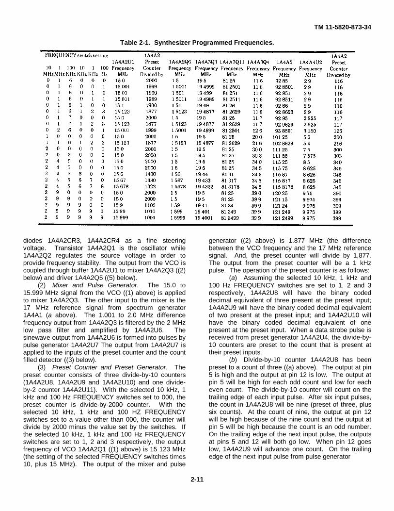
The synthesizer generates the three local oscillatorinjection frequencies used in the IF circuits of the radio.The 3rd local oscillator frequency is fixed at 10.5 MHzand is generated by spectrum generator 1A4A1 (abelow). The 2nd local oscillator frequency is fixed at80.75 MHz and is generated by translator 1A4A3 (cbelow). The 1st local oscillator frequency is variableand controls the operating frequency of the radio. The1st local oscillator frequency is generated by VCO1A4A5 (e below). The signals used to control the 1stlocal oscillator frequency are generated in other areas ofthe synthesizer. The frequency of some of these signalsis controlled by the setting of the selected FREQUENCYcontrol switches. Table 2-1 lists the points whereprogrammed frequencies and division ratios can befound in the synthesizer. The table also shows thefrequency or division ratio at these points for varioussettings of the selected FREQUENCY control switches.
a. Spectrum Generator 1A4A1 (Fig. FO-3 and Fig.FO-18).
(1) 20 MHz Reference Generator. The 5 MHzreference signal from TCXO 1A8U1 is amplified by1A4A1U1 and clipped by the diode clipper. The positivegoing half waves from the diode clipper are inverted by1A4A1U2A. The output of 1A4A1U2A is applied todivide-by-5 counter 1A4A1U4 ((2) below) and one shot1A4A1U2B, 1A4A1U2C. The 5 MHz pulse from the oneshot is inverted by 1A4A1U2D. The fourth harmonic ofthis 5 MHz pulse (20 MHz) is filtered by the 20 MHzbandpass filter and amplified by 1A4A1U33. The 20MHz pulse output from 1A4A1U3 is applied to low digitgenerator 1A4A2 (b below), 17 MHz mixer 1A4A1Q6((5) below) and 20 MHz amplifier 1A4A1U8 ((6) below).
(2) 1 MHz Reference Generator. The 5 MHzsignal from inverter 1A4A1U2A ((1) above) is applied todivide-by-5 counter 1A4A1U4. The 1 MHz output from1A4A1U4 is applied to divided-by-10 counter 1A4A1U5((3 below), through the 1 MHz bandpass filter toamplifier 1A4A1Q1, 1A4A1Q2 ((6) below) and to 3 MHzamplifier 1A4A1Q5 ((5) below).
(3) 100 kHz Reference Generator. The 1 MHzpulse from 1A4A1U4 ((2) above) is applied to divideby-10 counter 1A4A1U5 The 100 kHz output from1A4A1U5 is applied to VHF divider 1A4A4 (d below) andto divide-by-10 counter 1A4A1U6 ((4) below)
(4) 1 kHz Reference Generator. The 100 kHzpulse from 1A4A1U5 ((3) above) is applied to divideby-10 counter 1A4A1U6 The 10 kHz pulse from 1A4A1U6is applied to divlde-by-10 counter 1A4A1U7 The 1 kHzpulse from 1A4A1U7 is applied to low digit generator 1A4A2 (b below).
(5) 17 MHz Reference Generator. The thirdharmonic of the 1 MHz pulse from 1A4A1U4 ((2) above)is amplified by 3 MHz amplifier 1A4A1Q5. The 3 MHzoutput from 1A4A1Q5 is applied to 17 MHz mixer1A4A1Q6. The other input to 1A4A1Q6 is the 20 MHzsignal from 1A4A1U3 ((1) above). The two inputs aremixed in 1A4A1Q6 and the 17 MHz differencefrequency is filtered by the bandpass filter. The 17 MHzoutput of the bandpass filter is coupled through amplifier(complementary emitter follower) 1A4A1Q7, 1A4A1Q8to low digit generator 1A4A2 (b below).
(6) 21 MHz Reference Generator. The 1 MHzpulse from 1A4A1U4 ((2) above) is filtered by the 1 MHzbandpass filter. The 1 MHz sinewave from the 1 MHzbandpass filter is amplified by complementary emitterfollower 1A4A1Q1, 1A4A1Q2. The 1 MHz sinewavefrom the complementary emitter follower is applied tobalanced mixer 1A4A1CR4 thru 1A4AiCR7. The otherinput to be balanced mixer is the 20 MHz signal from1A4A1U3 ((1) above). The 20 MHz signal from1A4A1U3 is amplified by 1A4A1U8 and applied to thebalanced mixer. The 21 MHz sum frequency is filteredby the 21 MHz bandpass filter and amplified by1A4A1U9. The 21 MHz signal from 1A4A1U9 iscoupled through emitter follower 1A4A1Q9 to translator1A4A3 (c below).
(7) 10.5 MHz 3rd Local Oscillator Signal. The 21MHz signal from 1A4A1U9 ((6) above) is coupled todivide-by-2 counter 1A4A1U10. When the RT-1277/URC-92 is operating in the AM receive mode, or ifthe setting of the selected 1 MHz FREQUENCY switchis changed while transmitting switch 1A4A1Q3 is turnedon disabling 1A4A1U10. At all other times 1A4A1Q3 isoff and 1A4A1U10 divides the 21 MHz input by 2. The10.5 MHz output from 1A4A1U10 is coupled throughemitter follower 1A4A1Q4 to receiver/exciter 1A3.(para2-4).
b. Low Digit Generator 1A4A2 (Fig. FO-3 and Fig.FO-21)
(1) Voltage Controlled Oscillator 1A4A2. VCO1A4A2Q1, 1A4A2Q2 is a Colpitts oscillator with afrequency range of 15 0 to 15 999 MHz. The oscillatingfrequency of the VCO is equal to the setting of theselected 10 kHz, 1 kHz and 100 Hz FREQUENCYswitches times 10, plus 15 MHz. Coarse frequencytuning is provided by the action of the coarse frequencyvoltage (from the selected 10 kHz FREQUENCY switch)on varactor diodes 1A4A2CR1, 1A4A2CR2. Finefrequency control is provided by comparing the output ofthe VCO with the 17 MHz and 1 kHz signals fromspectrum generator 1A4A1 (a above). Phase detector1A4A2U2 ((4) below) develops an output voltage that isproportional to the difference between the frequency ofthe VCO and the desired frequency of the VCO Thisvoltage is applied to varactor
2-10
TM 11-5820-873-34
Table 2-1. Synthesizer Programmed Frequencies.
diodes 1A4A2CR3, 1A4A2CR4 as a fine steeringvoltage. Transistor 1A4A2Q1 is the oscillator while1A4A2Q2 regulates the source voltage in order toprovide frequency stability. The output from the VCO iscoupled through buffer 1A4A2U1 to mixer 1A4A2Q3 ((2)below) and driver 1A4A2Q5 ((5) below).
(2) Mixer and Pulse Generator. The 15.0 to15.999 MHz signal from the VCO ((1) above) is appliedto mixer 1A4A2Q3. The other input to the mixer is the17 MHz reference signal from spectrum generator1A4A1 (a above). The 1.001 to 2.0 MHz differencefrequency output from 1A4A2Q3 is filtered by the 2 MHzlow pass filter and amplified by 1A4A2U6. Thesinewave output from 1A4A2U6 is formed into pulses bypulse generator 1A4A2U7 The output from 1A4A2U7 isapplied to the inputs of the preset counter and the countfilled detector ((3) below).
(3) Preset Counter and Preset Generator. Thepreset counter consists of three divide-by-10 counters(1A4A2U8, 1A4A2U9 and 1A4A2U10) and one divide-by-2 counter 1A4A2U11). With the selected 10 kHz, 1kHz and 100 Hz FREQUENCY switches set to 000, thepreset counter is divide-by-2000 counter. With theselected 10 kHz, 1 kHz and 100 HZ FREQUENCYswitches set to a value other than 000, the counter willdivide by 2000 minus the value set by the switches. Ifthe selected 10 kHz, 1 kHz and 100 Hz FREQUENCYswitches are set to 1, 2 and 3 respectively, the outputfrequency of VCO 1A4A2Q1 ((1) above) is 15 123 MHz(the setting of the selected FREQUENCY switches times10, plus 15 MHz). The output of the mixer and pulse
generator ((2) above) is 1.877 MHz (the differencebetween the VCO frequency and the 17 MHz referencesignal. And, the preset counter will divide by 1,877.The output from the preset counter will be a 1 kHzpulse. The operation of the preset counter is as follows:
(a) Assuming the selected 10 kHz, 1 kHz and100 Hz FREQUENCY switches are set to 1, 2 and 3respectively, 1A4A2U8 will have the binary codeddecimal equivalent of three present at the preset input;1A4A2U9 will have the binary coded decimal equivalentof two present at the preset input; and 1A4A2U10 willhave the binary coded decimal equivalent of onepresent at the preset input. When a data strobe pulse isreceived from preset generator 1A4A2U4, the divide-by-10 counters are preset to the count that is present attheir preset inputs.
(b) Divide-by-10 counter 1A4A2U8 has beenpreset to a count of three ((a) above). The output at pin5 is high and the output at pin 12 is low. The output atpin 5 will be high for each odd count and low for eacheven count. The divide-by-10 counter will count on thetrailing edge of each input pulse. After six input pulses,the count in 1A4A2U8 will be nine (preset of three, plussix counts). At the count of nine, the output at pin 12will be high because of the nine count and the output atpin 5 will be high because the count is an odd number.On the trailing edge of the next input pulse, the outputsat pins 5 and 12 will both go low. When pin 12 goeslow, 1A4A2U9 will advance one count. On the trailingedge of the next input pulse from pulse generator
2-11
TM 11-5820-873-34
1A4A2U7, divide-by-10 counter 1A4A2U8 will assume acount of one instead of the preset count, since a datastrobe pulse was not received from preset generator1A4A2U4. Divide-by-10 counter 1A4A2U8 will have anoutput at pin 12 after every 10 input pulses until presetby the next data strobe pulse ((c) below).
(c) Divide-by-10 counter 1A4A2U9 has beenpreset to a count of two ((a) above). The outputs at pins5 and 12 are low. As described in ((b) above), 1A4A2U8will have 7 outputs after 67 inputs from 1A4A2U7. Afterseven outputs from 1A4A2U8, the count in 1A4A2U9 willbe nine (preset of two, plus seven counts). At the countof nine, the output at pin 12 will be high because of thenine count and the output at pin 5 will be high becausethe count is an odd number. On the trailing edge of thenext input pulse to 1A4A2U9 (77 inputs to 1A4A2U8),the outputs at pins 5 and 12 will both go low. When pin12 goes low, 1A4A2U10 will advance one count. On thetrailing edge of the next input pulse (87 inputs to1A4A2U8), 1A4A2U9 will assume a count of one insteadof the preset count, since a data strobe pulse was notreceived from preset generator 1A4A2U4. Divide-by-10counter 1A4A2U9 will have an output at pin 12 afterevery 10 input pulses (100 inputs to 1A4A2U8) untilpreset by the next data strobe pulse ((e) below).
(d) Divide-by-10 counter 1A4A2U10 has beenpreset to a count of one ((a) above). The output at pin 5is high and the output at pin 12 is low. As described m((b) and (c) above), 1A4A2U9 will have 8 outputs after777 inputs to 1A4A2U8. After eight outputs from1A4A2U9, the count in 1A4A2U10 will be nine (preset atone, plus eight counts). At the count of nine, the outputat pin 12 will be high because of the nine count and theoutput at pin 5 will be high because the count is an oddnumber. On the trailing edge of the next input pulse to1A4A2U10 (877 inputs to 1A4A2U8), the outputs at pins5 and 12 will both go low. When pin 12 goes low,1A4A2Ull will advance one count. On the trailing edgeof the next input pulse (977 inputs to 1A4A2U8),1A4A2U10 will assume a count of one instead of thepreset count, since a data strobe pulse was not receivedfrom preset generator 1A4A2U4. Divide-by-10 counter1A4A2U10 will go high at pin 12 after the next nine inputpulses (900 inputs to 1A4A2U8).
(e) The output from divide-by-two counter1A4A2Ull is high because the output from 1A4A2U10went low after 877 inputs to 1A4A2U8 ((d) above). After999 more inputs to 1A4A2U8 the count will be 1876. Allof the divide-by-10 counters will have a count of 9. Theoutputs at pin 5 will be high because the count is an oddnumber and the outputs at pin 12 will be high because ofthe nine count. The output from divide-by-two counter1A4A2U11 is still high because the output of 1A4A2U10
has not gone low. With the exception of the input that isconnected to pulse generator 1A4A2U7, all of the inputsto count filled detector 1A4A2U3 are high. On the nextoutput pulse from pulse generator 1A4A2U7, the countwill be 1877 (the preset count) When the output from1A4A2U7 goes high, it will put a high on the only input to1A4A2U3 that is low and 1A4A2U3 will output a 50nanosecond pulse. On the trailing edge of the pulsefrom 1A4A2U3 preset generator 1A4A2U4 will output a75 nanosecond pulse. The output from 1A4A2U4 iscoupled to phase detector 1A4A2U2 ((4) below) and tothe data strobe inputs of the preset counter
(4) Phase Detector and Loop Filter. Phasedetector 1A4A2U2 compares the output frequency of thepreset counter ((3) above) with the 1 kHz referencesignal from spectrum generator 1A4A1 (a above) anddevelops a DC output voltage that is proportional to thetwo signals. The output of the preset counter will be 1kHz when the VCO is operating at the desired frequencyIf the output of the VCO is high, the output frequency ofthe preset counter will be less than 1 kHz. The outputvoltage from the phase detector will decrease, causingthe operating frequency of the VCO to decrease. If theoutput of the VCO is low, the output frequency of thepreset counter will be more than 1 kHz. The outputvoltage from the phase detector will increase, causingthe operating frequency of the VCO to increase. Theloop filter removes any 1 kHz components in the phasedetector output and also determines the transientresponse of the loop.
(5) Output Divider. The output from buffer1A4A2U1 ((1) above) is amplified by driver 1A4A2Q5.Divide-by-10 counter 1A4A2U5 divides the signal from1A4A2Q5 and the 1.50 to 1.5999 MHz output signal isfed through the 1 55 MHz bandpass filter and emitterfollower 1A4A2Q6 to translator 1A4A3 ((c) below).
c. Translator 1A4A3 (Fig. FO-3 and FO-20)(1) Voltage Controlled Crystal Oscillator. With
the VFO control pulled out (on), + 12 volts is applied to21 MHz reference amplifier 1A4A3U1 disabling theamplifier. The same + 12 volts turns voltage controlledcrystal oscillator 1A4A3Q1 and switch 1A4A3Q3.Turning on 1A4A3Q3 enables amplifier 1A4A3U2.1A4A3Q1 is a crystal controlled Colpitts oscillatoroperating In the frequency range of 20.995 to 21 005MHz. The control voltage from the VFO control isapplied through control amplifier 1A4A3Q3 to thevaractor diodes in the circuit to control the operatingfrequency of 1A4A3Q1. The output from 1A4A3Q1 isamplified by 1A4A3U2 and applied to the 19 MHzbalanced mixer ((3) below).
(2) 21 MHz Reference Amplifier. With the VFOcontrol pushed in (off), 1A4A3Q1 and 1A4A3U2 are
2-12

TM 11-5820-873-34
disabled and 21 MHz reference amplifier 1A4A3U1 isenabled. The 21 MHz reference signal from spectrumgenerator 1A4A1 (a above) is amplified by 1A4A3U1and applied to the 19 MHz balanced mixer ((3) below).
(3) 19 MHz Balanced Mixer. The 21 MHz signalfrom the 21 MHz reference amplifier ((2) above) or thevoltage controlled crystal oscillator ((1) above) is mixedwith the 1.50 to 1.5999 MHz signal from low digitgenerator 1A4A2 (b above) in the 19 MHz balancedmixer. The difference frequency output is filtered by the19.45 MHz bandpass filter and amplified by 1A4A3U3.Diodes 1A4A3CR5 and 1A4A3CR12 provide AGC toamplifier 1A4A3U3 to ensure a constant level 19.4001to 19.50 MHz signal out. The 19.4001 to 19.50 MHzsignal from 1A4A3U3 is applied to 81.25 MHz mixer1A4A3Q11 (6) below.
(4) 2nd Local Oscillator. The 2nd local oscillatoris a crystal controlled Colpitts oscillator operating at80.75 MHz. The output from 2nd local oscillator1A4A3Q7 is applied to 100 MHz mixer 1A4A3Q8 ((5)below) and through buffer amplifier 1A4A3Q9 toreceiver/exciter 1A3 (para 2-4).
(5) 100 MHz Mixer. The 80.75 MHz signal fromthe 2nd local oscillator ((4) above) is mixed with the 20MHz reference signal from spectrum generator 1A4A1(a above) in 100 MHz mixer 1A4A3Q8. The sumfrequency output is filtered by the 100.75 MHz bandpassfilter and applied to 81.25 MHz mixer 1A4A3Q11 ((6)below)
(6) 81.25 MHz Mixer. The 100.75 MHz signalfrom the 100.75 MHz bandpass filter ((5) above) ismixed with the 19.4001 to 19.50 MHz signal from1A4A3U3 ((3) above) in 81.25 MHz mixer 1A4A3Q11.The difference frequency output is filtered by the 81.25MHz bandpass filter and applied to output mixer1A4A3Q4 ((7) below).
(7) Output Mixer. The 81.25 to 81.3499 MHzsignal from the 81.25 MHz bandpass filter ((6) above) ismixed with the 91.25 to 121.2499 MHz signal from VCO1A4A5 (e below). The frequency of the 81.25 to81.3499 MHz signal represents the setting of theselected 10 kHz, 1 kHz and 100 HZ FREQUENCYswitches. The frequency of the 91.25 to 121.2499 MHzsignal represents the setting of all of the selectedFREQUENCY switches. Since the 10 kHz, 1 kHz and100 Hz frequency components are present in bothsignals, they will cancel in the output mixer when theoutput of the synthesizer is at the correct frequency(normal operating condition). Therefore, the signal fromoutput mixer 1A4A3Q4 will only represent the setting ofthe selected 10 MHz, 1MHz and 100 kHz FREQUENCYswitches, and will change in 100 kHz steps. The 10.0 to39.9 MHz difference frequency signal from output mixer1A4A3Q4 is amplified by the broadband amplifier andapplied to VHF divider 1A4A4 (d below).
d. VHF Divider 1A4A4 (Fig. FO-3 and Fig. FO-21).(1) Broadband Amplifier, Divide-by-Four Counter,
and Driver. The 10.0 to 39.9 MHz signal from translator1A4A3 (c above) is amplified and applied to divide-by-four counter 1A4A4U2. The 2.5 to 9.975 MHz signalfrom 1A4U2 is inverted by driver 1A4A1U1 and appliedto the inputs of the preset counter and the presetgenerator ((2) below).
(2) Preset Counter, Carry Detector and PresetGenerator. The preset counter and preset generator aresimilar to the preset counter and preset generator in thelow digit generator (b(3) above). The major differencesare a carry detector is used when the selected 100 kHzFREQUENCY switch is set to 0 and divide-by-fourcounter 1A4A4U7 is preset by the 10 MHz preset gateinstead of directly from the selected 10 MHzFREQUENCY switch.
(a) Preset Counter. The preset counterconsists of two divide-by-10 counters (1A4A4U3 and1A4A4U6) and one divide-by-four counter (1A4A4U7).The counter will divide by the number the selected 10MHz, 1 MHz and 100 kHz FREQUENCY switches areset at plus 100 (table 2-1).
(b) Carry Detector. When all four 100 kHzpreset lines are programmed to a 0 state by the frontpanel switches (corresponding to a dial setting of 0 onthe selected 100 kHz FREQUENCY switch), a specialcarry signal must be generated to program the countersto the correct division ratio. Mathematically, this isnecessary because a dial setting of zero requires1A4A4U3 to divide by zero-an impossible operation.The count is corrected by programming 1A4A4U3 todivide-by-ten and then subtracting one count from thenext decade counter. Note that this is the samemathematical operation of borrowing when, for example,one subtracts nine from ten. Quad two input NAND gate1A4A4U4 is connected as a quad inverter with acommon output. One of the four 100 kHz input lines isconnected to each section of the gate. The output of1A4A4U4 is inverted by 1A4A4U5A. If all four inputs to1A4A4U4 are zero, the output of 1A4A4U4 will be in aone state and the 1A4A4U5A output will be a zero. Ifany of the 100 kHz inputs are in a one state, the1A4A4U5A output will also be a one.
(c) Count Filled Detector. The inputs countfilled detector 1A4A4U8C, 1A4A4U9 are similar to theinputs to count filled detector 1A4A3U3 described inb(3)(e) above. However, the input at pin 5 will alwaysbe high if the selected 100 kHz FREQUENCY switch isset to zero. If the selected 100 kHz FREQUENCYswitch is set to a number other than zero, the input atpin 5 will follow the output at pins 5 and 6 of 1A4A4U6.The output from the count filled detector is a 400nanosecond positive pulse.
(d) Preset Generator. Preset generator 115A4A4U10 provides a 200 nanosecond negative data
2-13
TM 11-5820-873-34
strobe pulse when it is triggered by the pulse from thecount filled detector ((c) above)
(3) Phase Detector. The 100 kHz referencesignal from spectrum generator 1A4A1 (a above) isapplied to divide-by-four counter 1A4A4U11. The 25kHz output from 1A4A4U11 is applied to phase detector1A4A4U12. The phase detector compares the nominal25 kHz output frequency of the preset counter ((2)above) with the 25 kHz input from 1A4A4U11 anddevelops a DC output voltage that is proportional to thetwo signals. The output from the phase detector iscoupled to VCO 1A4A5 (e below).
e. VCO 1A4A5 (Fig. FO-3 and Fig. FO-11).(1) Band Oscillators. The selected 10 MHz
FREQUENCY switch enables one of the three bandoscillators through one of the three transistor switches.The band oscillators are Colpitts oscillators similar tovoltage controlled oscillator 1A4A2 (b(1) above). Band0 oscillator 1A4A5Q7 operates over a frequency rangeof 91.25 to 101.2499 MHz Band 1 oscillator 1A4A5Q7operates over a frequency range of 101.25 to 111.2499MHz. And, Band 2 oscillator 1A4A5Q8 operates over afrequency range of 111.25 to 121.2499 MHz. Coarsefrequency tuning is provided by the action of the coursefrequency voltage from the selected 10 MHzFREQUENCY switch. Fine frequency tuning is providedby the DC voltage from VHF divider 1A4A4 (d(3)above). The output from the enabled band oscillator iscoupled through amplifier 1A4A5Q11, 1A4A5Q12 totranslator 1A4A3 (c above) and through amplifier1A4A5Q9, 1A4A5Q10 and the 91 to 122 MHz bandpassfilter to receiver/exciter 1A3 (para 2-4).
(2) Binary Coded Decimal Converter. The BCDconverter consists of two transistor switches, 1A4A5Q1and 1A4A5Q2, that convert the ground signal from theselected 10 MHz FREQUENCY switch to tenscomplement binary coded decimal. The output from theBCD converter is applied to the 10 MHz preset gate(d(2) above) in VHF divider 1A4A4.
f. Local Oscillator Blanker (Fig. FO-23). The localoscillator blanker protects the power amplifier fromtransients caused by a frequency change whiletransmitting. When the selected 1 MHz FREQUENCYswitch setting is changed, the synthesizer may changefrequency by several MHz while the switch ismomentarily open. If this occurs while transmitting, itwould result in a large transient that could damage RFpower amplifier 1A7A1.
When the setting of the selected 1 MHzFREQUENCY switch is changed, the "preset 20 1 MHz"frequency control line will change from either:
logical "0" (approximately 0.2 volts) tological "1" (approximately 3 volts) stateorlogical "1" to logical "0" state
In the first case, the positive going signal is formed intoa 100 to 200 millisecond positive differentiated pulse.The positive differentiated pulse turns switch 1A4A6Q2on Switch 1A4A6Q2 turns switch 1A4Q6Q1 on,generating a blanking pulse. In the second case, thenegative going signal is formed into a 100 to 200millisecond negative differentiated pulse The negativedifferentiated pulse turns switch 1A4A6Q1 on,generating a blanking pulse In either case, the blankingpulse is applied to spectrum generator 1A4A1 (a above),and disables the 3rd local oscillator signal.
2-10. Filter Module 1A5 Detailed FunctionalOperation (Fig. FO-4)
a. Filtering. The filter module provides low passfiltering in transmit mode and band pass in receivemode. The filters have been divided among threedifferent boards. Board 1A5A1 has the low pass filtersfor the odd number channels. Board 1A5A2 has the lowpass filters for the even number channels. Board1A5A3 has high pass filters. Only the low pass filtersare used in the transmit mode. The high pass filters areused, along with the low pass filters, for band passfiltering in the receiver mode. Correct filtering for eachband is accomplished automatically when the frontpanel frequency control switches are set. Inactivefilters, for any given band, are switched to groundthrough a 10 ohm resistor. This discharges the filter andprevents unwanted interaction with active filters. Table2-2 lists the filter band numbers and their correspondingfrequency ranges.
Table 2-2. Band Numbers and Frequency Ranges.
b. Filter Selection. Correct filter selection for theband in use is setup through wafer switches driven by aDC motor. The motor (B1) is mounted on the MotorControl Board 1A5A4. Motor control is accomplishedwith an "open seeking" circuit comprised of relay1A5A4K1 and wafer switch 1A5A4S1. When changingthe 1 MHz or 10 MHz switch of the selected frequencychanges the band, relay 1A5A4K1 is energized thru1A5A4S1. The now closed contacts, 5 and 9, of1A5A4K1 supply + 12 VDC to motor 1A5A4B1. Themotor simultaneously rotates the wafer switches on
2-14
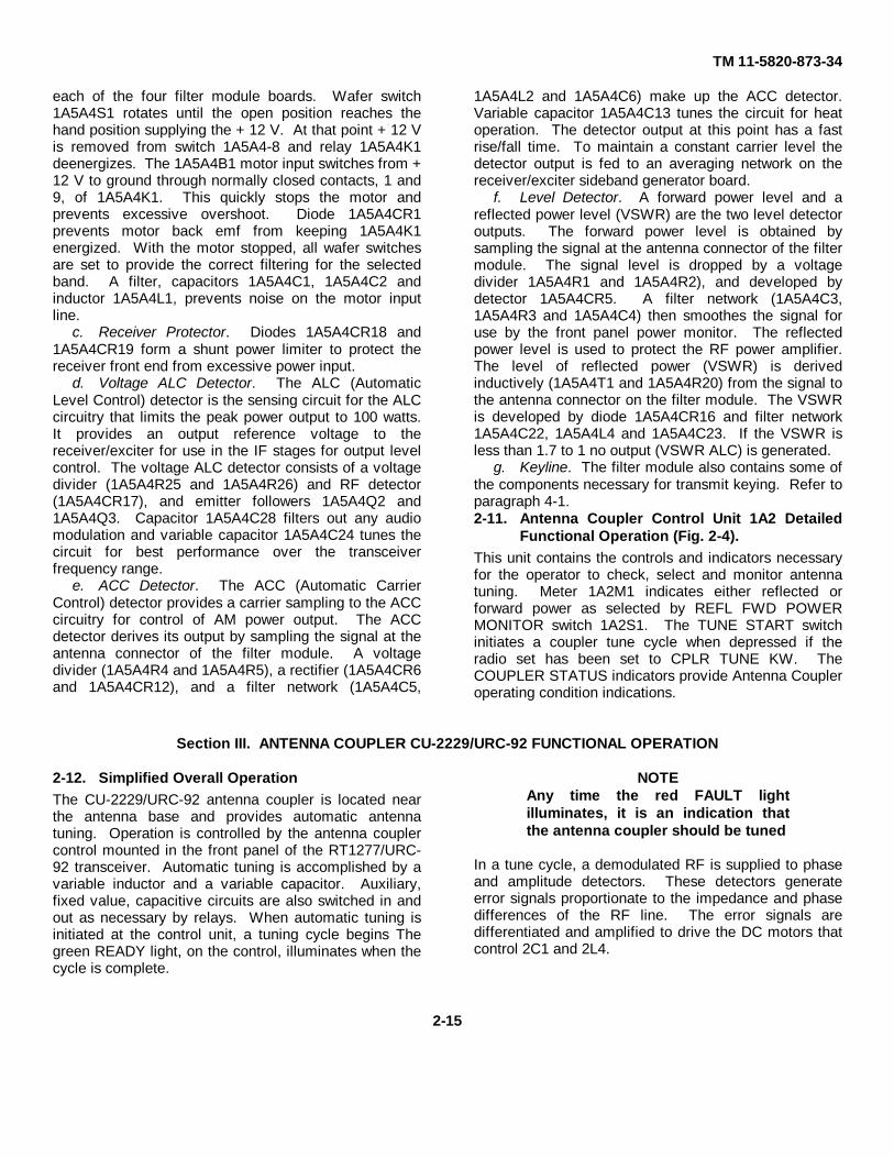
TM 11-5820-873-34
each of the four filter module boards. Wafer switch1A5A4S1 rotates until the open position reaches thehand position supplying the + 12 V. At that point + 12 Vis removed from switch 1A5A4-8 and relay 1A5A4K1deenergizes. The 1A5A4B1 motor input switches from +12 V to ground through normally closed contacts, 1 and9, of 1A5A4K1. This quickly stops the motor andprevents excessive overshoot. Diode 1A5A4CR1prevents motor back emf from keeping 1A5A4K1energized. With the motor stopped, all wafer switchesare set to provide the correct filtering for the selectedband. A filter, capacitors 1A5A4C1, 1A5A4C2 andinductor 1A5A4L1, prevents noise on the motor inputline.
c. Receiver Protector. Diodes 1A5A4CR18 and1A5A4CR19 form a shunt power limiter to protect thereceiver front end from excessive power input.
d. Voltage ALC Detector. The ALC (AutomaticLevel Control) detector is the sensing circuit for the ALCcircuitry that limits the peak power output to 100 watts.It provides an output reference voltage to thereceiver/exciter for use in the IF stages for output levelcontrol. The voltage ALC detector consists of a voltagedivider (1A5A4R25 and 1A5A4R26) and RF detector(1A5A4CR17), and emitter followers 1A5A4Q2 and1A5A4Q3. Capacitor 1A5A4C28 filters out any audiomodulation and variable capacitor 1A5A4C24 tunes thecircuit for best performance over the transceiverfrequency range.
e. ACC Detector. The ACC (Automatic CarrierControl) detector provides a carrier sampling to the ACCcircuitry for control of AM power output. The ACCdetector derives its output by sampling the signal at theantenna connector of the filter module. A voltagedivider (1A5A4R4 and 1A5A4R5), a rectifier (1A5A4CR6and 1A5A4CR12), and a filter network (1A5A4C5,
1A5A4L2 and 1A5A4C6) make up the ACC detector.Variable capacitor 1A5A4C13 tunes the circuit for heatoperation. The detector output at this point has a fastrise/fall time. To maintain a constant carrier level thedetector output is fed to an averaging network on thereceiver/exciter sideband generator board.
f. Level Detector. A forward power level and areflected power level (VSWR) are the two level detectoroutputs. The forward power level is obtained bysampling the signal at the antenna connector of the filtermodule. The signal level is dropped by a voltagedivider 1A5A4R1 and 1A5A4R2), and developed bydetector 1A5A4CR5. A filter network (1A5A4C3,1A5A4R3 and 1A5A4C4) then smoothes the signal foruse by the front panel power monitor. The reflectedpower level is used to protect the RF power amplifier.The level of reflected power (VSWR) is derivedinductively (1A5A4T1 and 1A5A4R20) from the signal tothe antenna connector on the filter module. The VSWRis developed by diode 1A5A4CR16 and filter network1A5A4C22, 1A5A4L4 and 1A5A4C23. If the VSWR isless than 1.7 to 1 no output (VSWR ALC) is generated.
g. Keyline. The filter module also contains some ofthe components necessary for transmit keying. Refer toparagraph 4-1.2-11. Antenna Coupler Control Unit 1A2 Detailed
Functional Operation (Fig. 2-4).This unit contains the controls and indicators necessaryfor the operator to check, select and monitor antennatuning. Meter 1A2M1 indicates either reflected orforward power as selected by REFL FWD POWERMONITOR switch 1A2S1. The TUNE START switchinitiates a coupler tune cycle when depressed if theradio set has been set to CPLR TUNE KW. TheCOUPLER STATUS indicators provide Antenna Coupleroperating condition indications.
Section III. ANTENNA COUPLER CU-2229/URC-92 FUNCTIONAL OPERATION
2-12. Simplified Overall OperationThe CU-2229/URC-92 antenna coupler is located nearthe antenna base and provides automatic antennatuning. Operation is controlled by the antenna couplercontrol mounted in the front panel of the RT1277/URC-92 transceiver. Automatic tuning is accomplished by avariable inductor and a variable capacitor. Auxiliary,fixed value, capacitive circuits are also switched in andout as necessary by relays. When automatic tuning isinitiated at the control unit, a tuning cycle begins Thegreen READY light, on the control, illuminates when thecycle is complete.
NOTEAny time the red FAULT lightilluminates, it is an indication thatthe antenna coupler should be tuned
In a tune cycle, a demodulated RF is supplied to phaseand amplitude detectors. These detectors generateerror signals proportionate to the impedance and phasedifferences of the RF line. The error signals aredifferentiated and amplified to drive the DC motors thatcontrol 2C1 and 2L4.
2-15
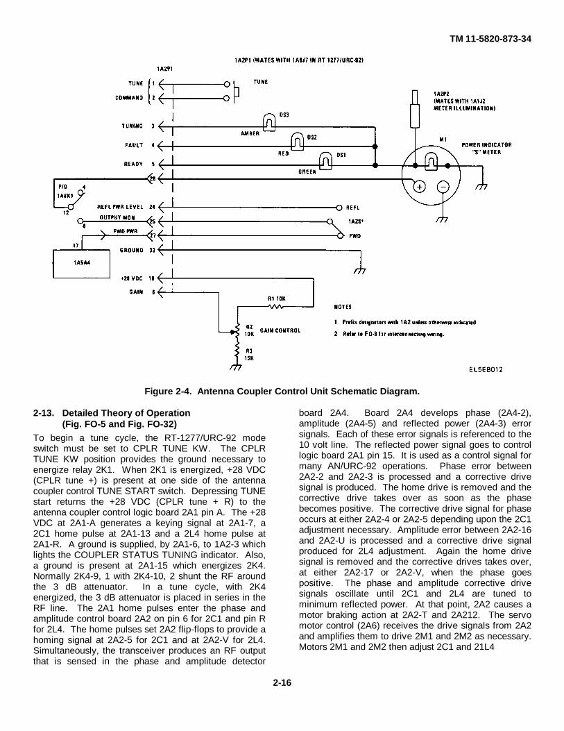
TM 11-5820-873-34
Figure 2-4. Antenna Coupler Control Unit Schematic Diagram.
2-13. Detailed Theory of Operation(Fig. FO-5 and Fig. FO-32)
To begin a tune cycle, the RT-1277/URC-92 modeswitch must be set to CPLR TUNE KW. The CPLRTUNE KW position provides the ground necessary toenergize relay 2K1. When 2K1 is energized, +28 VDC(CPLR tune +) is present at one side of the antennacoupler control TUNE START switch. Depressing TUNEstart returns the +28 VDC (CPLR tune + R) to theantenna coupler control logic board 2A1 pin A. The +28VDC at 2A1-A generates a keying signal at 2A1-7, a2C1 home pulse at 2A1-13 and a 2L4 home pulse at2A1-R. A ground is supplied, by 2A1-6, to 1A2-3 whichlights the COUPLER STATUS TUNING indicator. Also,a ground is present at 2A1-15 which energizes 2K4.Normally 2K4-9, 1 with 2K4-10, 2 shunt the RF aroundthe 3 dB attenuator. In a tune cycle, with 2K4energized, the 3 dB attenuator is placed in series in theRF line. The 2A1 home pulses enter the phase andamplitude control board 2A2 on pin 6 for 2C1 and pin Rfor 2L4. The home pulses set 2A2 flip-flops to provide ahoming signal at 2A2-5 for 2C1 and at 2A2-V for 2L4.Simultaneously, the transceiver produces an RF outputthat is sensed in the phase and amplitude detector
board 2A4. Board 2A4 develops phase (2A4-2),amplitude (2A4-5) and reflected power (2A4-3) errorsignals. Each of these error signals is referenced to the10 volt line. The reflected power signal goes to controllogic board 2A1 pin 15. It is used as a control signal formany AN/URC-92 operations. Phase error between2A2-2 and 2A2-3 is processed and a corrective drivesignal is produced. The home drive is removed and thecorrective drive takes over as soon as the phasebecomes positive. The corrective drive signal for phaseoccurs at either 2A2-4 or 2A2-5 depending upon the 2C1adjustment necessary. Amplitude error between 2A2-16and 2A2-U is processed and a corrective drive signalproduced for 2L4 adjustment. Again the home drivesignal is removed and the corrective drives takes over,at either 2A2-17 or 2A2-V, when the phase goespositive. The phase and amplitude corrective drivesignals oscillate until 2C1 and 2L4 are tuned tominimum reflected power. At that point, 2A2 causes amotor braking action at 2A2-T and 2A212. The servomotor control (2A6) receives the drive signals from 2A2and amplifies them to drive 2M1 and 2M2 as necessary.Motors 2M1 and 2M2 then adjust 2C1 and 21L4
2-16
TM 11-5820-873-34respectively to the correct position for minimumreflected power When reflected power has beenadjusted below the threshold, control logic board 2A1ends the tune cycle The COUPLER STATUS READYIndicator is illuminated by a ground at 2A1-N and theAN/URC-92 is ready for transmitting2-14. Control Logic Board 2A1 Detailed
Functional Operation(Fig FO-6 and Fig FO-33)
Board 2A1 provides control co-ordination for theautomatic tuning cycle The logic outputs of 2A1 provideinitiation, cycling, completion and fault signals Thecontrol logic board Is divided into eight functional blockswhich will he discussed Individually The eight functionsare Tune flip-flop, 50 ohm flip-flop, Fault flip-flop, TimeDelay, C3-C6 control, Reflected Power Amp, RFDetector, and Lamp Driver
a. Tune Flip-Flop The Tune flip-flop is comprised of2A1Q10, 2AlQ15, 2A1U3B-C-D, 2A1U4C-D and allrelated components When the unit is first turned on,2A1U3B-6 is at a logic 0 due to circuit loading.Depressing the TUNE START pushbutton on theantenna coupler control (1A2) applied + 28 VDC to2XA1-A The +28 VDC turns on 2A1Q15, causing a logic0 at the collector, which initiates a tune cycle The logic 0initiate signal resets 2AIU3C-8 causing a logic 1 at2A1U3B-6 Because of this, 2AlQ10 turned on andground the Interlock (2XA1-7) which keys the transmitteron in am The 2AlU: 3B-6 output is also fed to the LampDriver to light the COUPLER STATUS TUNINGIndicator The same logic 0 initiate signal is used in allthe other functions except the [,amp l)river It alsoprovides the 2C1 home (2XA1-13) and 2I,L4 home(2XA1-R) outputs The Tune FF is reset, when the tunecycle ends, by a logic 1 at 2AlU4C-9 from the ReflectedPower Amp which produces logic 0 at 2AlU4C-8 Thatlogic 0 resets the Fault FF and the Tune FF whichextinguishes the COUPILER STATUS TUNNG IndicatorAt the same time 2A1U41)-11 is at a logic 1 which is fedto the Lamp Driver to light the COUPLER STATUSREAI)Y indicator
b. 50 Ohm Flip-Flop The 50 Ohm FF includes2AlQ13, 2A1Q19 1A1U6A-B C-D, 2A1U4C andassociated components When a tune cycle is Initiated, alogic 0 is placed at 2AlU6C-8 and sets the FF with alogic 1 at 2AlU6D-11 The logic 1 triggers 2A1Q14 toprovide a ground, for energizing 2K4, at 2XA1-15Energizing 2K4 switches the 3 dB attenuator in serieswith the rf transmission line When reflected power dropsbelow threshold or RF power is not sensed by the RFDetector, the 50 Ohm FF is reset This causes 2A1Q14to cease conduction and 2K4 deenergizes, taking the 3dB attenuator out of the transmission line If the reflectedpower is below threshold, 2A1Q3
of the Reflected Power Amp develops logic 0 at U6A-1Gate 2A1U6A then establishes logic 1 at 2A1U6B-4 and2XA1-14, which is the 50 (+) output. Gate 2A1U6Bgenerates logic 0 at 2AIU6C-9 to reset the FF If RF isnot present during a tuning cycle, the FF also resets butis set again by 2A1Q19 and 2A1U5C. The 50 Ohm FFis also set, and triggers 2A1Q14 if any of the followingconditions occur the Time Delay running out or variableinductor 2L4 reaching L max will set the FF thru2A1CR15 and/or 2A1CR16 respectively. Also, somefrequency-impedance combinations may cause the FFto reset and the tuner will not tune. This situation occursif reflected power rises above threshold during the sametune cycle Then an RC network, 2A1R29 and 2A1C36,charges to trigger 2AlQ13 Then 2A1Q13 established alogic 0 at 2A1U6D-13 to set the FF, 2A1U6D1 1, at logic1 and trigger 2A1Q14 on. With that the 3 dB attenuatorIs again switched in to prevent transmitting into apossible open or short circuit.
c. Fault Flip-Flop. The Fault FF consists of 2A1U4A-B,2A1U5A-B-D, 2AICR12, 2A1CR13 and theircorresponding circuits When power is first applied(transceiver turned on), circuit loading causes 2A1U4B-6to be logic 0 and set the FF The logic 1 at 2alU4A-3 Isthen fed to the Lamp Driver to light the COUPLERSTATUS FAULT indicator. When the mode switch isset to CPLR TUNE KW, +10V is switched to 2XA1-2thru 2K1. The + 10V is applied to an RC network andvoltage regulator, in the Fault FF to generate a singlelogic 1 pulse This pulse is inverted by 2A1U5D and thelogic 0 makes 2A1U4B-6 a logic 0 The logic 0 is also fedto Tune FF 2A1U3D-13 to extinguish the CPLR TUNEREADY indicator The output of 2A1U4A-3 is then atlogic 1 and fed to the Lamp Driver to light theCOUPLER STATUS FAULT indicator The Fault FF isalso set by a logic 0 from 2A1U5A-11. A logic 0 from2A1U5A is caused when two conditions are met First,the reflected power is above threshold and ReflectedPower Amp 2A1Q3 causes a logic 1 at 2A1U5A-13.Second, Tune FF 2A1U3C-8 produces a logic 1 at2A1U5A-12, indicating tuning is not in process Thisensures. the COUPLER STATUS FAULT indicator willlight any time timing is required due to antenna orfrequency change If the Time Delay runs out, the FaultFF will he set with a logic 0 from 2A1CR20 to 2A1U4B-6.
d. Reflected Power Amp Components2A101.2A1Q1, 2A1Q2, 2A1Q3. 2A1Q4, 2A1Q5,2A1CR1, 2A1CR2 and associated resistors andcapacitors make up the Reflected Power Amp From2X1A-3 a DC voltage, proportionate to reflected poweron the transmission line, is fed to 2A1U1-4. This signalIs referenced to + 10 VDC and 2AlU1 develops itsoutput from that reference. The output at 2A1U1-10,along with a gain input (2XA1-8) from the antenna
2-17
TM 11-5820-873-34
coupler control, controls 2A1Q1 operation The gaininput establishes the reflected power threshold thatcauses 2A1Q1 conduction Transistor 2A1Q2 convertsthe 2A1Q1 output into an on/off output characteristic ofreflected power When 2A1Q2 conducts, it representsreflected power above threshold With 2A1Q2 off,reflected power Is below threshold and a positivevoltage is felt at the base of 2A1Q3 Transistor 2A1Q3conducts when reflected power is below threshold andits collector is at ground The 50 (-) output of board 2A1,at 2XA1-8, is taken from the collector of 2A1Q3 Also,2A1Q3 drives 2A1Q4 Transistor 2A1Q4 and associatedcomponents establish a short time delay The time delayprevents brief intervals of reflected power drop fromterminating a tuning cycle The 2A1Q4 output operates2A1Q5 to provide logic outputs characteristic ofreflected power level A logic 1 from 2A1Q5 indicatesreflected power below threshold The logic 1 is fed toTune FF 2A1U4C-9 to terminate the tune cycle Diode2AlCR1 and resistor 2A1R7 in the Reflected Power Ampcut it off during receive mode This prevents keyingspikes from causing the CPLR STATUS FAULTindicator to come on when unkeying.
e. Time Delay. The time delay consists of2A1Q16, 2AlQ17, 2AlQ18 and their related componentsVariable resistor 2A1R46 adjusts the length of the timedelay The normal time delay setting should beapproximately 40 seconds Time Delay operation is asfollows When a tune cycle is initiated, the collector of2A1Q16 rises to near +VDC Capacitor 2A1C40 beginscharging thru 2A1R47 and the anode of 2A1Q17increases toward +5 VDC Transistor 2A1Q17 is aprogrammable unifunction transistor that fires when theanode voltage reaches the voltage applied to the gateVoltage divider 2A1R49 and 2AlR50 sets the gatevoltage at approximately +5 VDC When 2A1Q17 fires,the positive pulse triggers 2A1Q18 and 2A1Q18collector produces a logic 0. The logic 0 resets theTune FF thru 2A1CR21 and the Fault FF thru 2A1CR20.This terminates the tune cycle and lights the CPLRSTATUS FAULT indicator Diode 2A1CR26 places alogic 0 on the L max line to terminate the L forcefunction at the end of the time delay.
f. RF Detector. The RF Detector is comprised of2A1Q8 and its associated components. When RF Issensed on the transmission line, a DC signal is presentat 2XA1-B This signal is coupled into the RF detectorthru an RC network, 2A1R23 and 2A1C34 The RCnetwork allows 2A1Q8 to trigger on only when aconstant DC level is present Erratic levels and spikesare shunted to ground through 2A1C34. This preventsnoise from turning the antenna tuner off when thetransmitter is first keyed on when 2A1Q8 triggers on, alogic 0 is generated at the collector and inverted by2A1U3. The logic 1 from 2A1U3-3 is fed to the Fault FF(2A1U4C-10) and the 50 ohm FF (2A1U6B-5).
g. C3/C6 Control Assembly. Components 2A1Q6,2A1Q7, 2A1U2 and their associative circuitry make upthe C3/C6 control Capacitor 2C3 is switched in and outof the circuit in the following way. Each time the timedelay runs out, 2A1U2C inverts the logic 0 from TimeDelay 2AlQ18 to logic 1. The logic 1 (2A1U2-8) thentriggers 2A1Q6 to provide a ground at 2XA1-17 whichenergizes bistable relay 2A5K2. Bistable relay 2A5K2 isthe control for 2K3 which controls 2C3A-B Control of2C6 also utilizes a bistable relay, 2A5K1 It is controlledby 2A1U2A-B-D The L max signal, a logic 0, is producedwhen 2L4 reaches maximum inductance. This logic 0comes in on 2XA1-T to 2A1U2D and is inverted. Thelogic 1 at 2A1UD-11 then triggers 2A1Q7 to provide aground at 2XA1-V. That ground toggles 2A5K1 into itsopposite state. This action either switches 2C6 in or outacross 2L4, depending on its previous condition. If 2C6is switched across the 2L4, +28 VDC is also switched onto 2XA1-U. This +28 VDC is reduced to a logic 1 levelby voltage divider 2A1R19 and 2A1R20. The logic 1 isthen fed to 2A1U2B-5 and a logic 0 is then present at2A1U2B-6. That logic 0 is inverted by 2A1U2D andagain 2A1Q7 is triggered Bistable relay 2A5K1 istoggled into its opposite state and 2C6 is either switchedin or out across 2L4. It should be noted that if 2L4reaches L min and 2K2 is not energized, 2A5K1 will notbe toggled. Also, if a tune cycle is initiated, 2A1U2Ahas a logic 0 output. At this time, if 2C6 is across 2L4, itwill be removed.
h. Lamp Driver. The three CPLR STATUSindicators, on the antenna coupler control, are controlledby 2A1Q9, 2A1Q11 and/or 2A1Q12. These lampdrivers are turned on by logic signals at the appropriatetimes. The CPLR STATUS FAULT lamp driver is2A1Q12. It is triggered on anytime the Fault FF has alogic 1 at 2A1U4A-3 Lamp driver 2A1Q11 lights theCPLR STATUS READY indicator. This happens with alogic 1 from the Tune FF at 2A1U4D11 CPLR STATUSis lit by 2A1Q9 with a logic 1 from Tune FF 2A1U3B-6.
2-15. Phase and Amplitude ControlBoard 2A2 Detailed Functional Operation
(Fig FO-7 and FO-34)
Board 2A2 processes inputs from Phase and AmplitudeDetector 2A4 to provide drive signals for Servo MotorControl 2A6. Thirteen functions are contained on 2A2.These functions are: Phase Preamp, Phase LevelChanger, Phase Positive Logic Generator, C1 Home-Flip-Flop, C1 Drive Inhibit, Phase Servo Preamp,Amplitude Preamp, Amplitude Level Changer, L4 HomeFlip-Flop, L4 Force Flip-Flop, L4 Drive Inhibit, AmplitudeServo Preamp and Phase/Amplitude Brake.
2-18
TM 11-5820-873-34
a Phase Preamp. The Phase Preamp consists ofdifferential amplifier 2A2U1, 2A2CR1, 2A2CR2 andrelated components. A + 10 VDC reference is appliedto 2A2U1-4. The 2A2U1-5 input is a DC levelproportionate to phase angle. The 2A2U1-10 output isreferenced at a + 10 VDC level which is the null outputlevel. When phase angle goes negative, 2A2U1-10generates a corresponding output level below +10 VDC.If phase angle is positive, 2A2U1-10 is at acorresponding level above +10 VDC Operational levelsof 2A2U1-10 are between ground and +28 VDC.
b. Phase Level Changer. Components of thisfunction are 2A2Q1, 2A2Q2, 2A2Q3 and associatedcircuitry. An input, to the Phase Level Changer, above+10 VDC controls 2A2Q1 conduction Transistor 2A2Q1output, in turn, controls 2A2Q3 which establishes a drivesignal to the Phase Servo Preamp positive drive. Also2A2Q3 provides an output to the Phase Positive LogicGenerator. If the Phase Level Changer input is below +10 VDC, 2A2Q2 conducts to provide a drive signal tothe Phase Servo Preamp negative drive.
c Phase Positive Logic Generator. Transistor2A2Q4 functions as a logic level generator. Whentriggered by the Phase Level Changer, it establishes alogic level 0. This logic 0 indicates a positive phaseangle to board 2A2 flip-flop functions.
d. C1 Home Flip-Flop. The C1 Home flip-flop iscomprised of 2A2U2A-B-C, 2A2Q5, 2A2CR3, 2A2CR4,2A2CR5 and associated components When power isfirst applied, this FF resets and 2A2U2A-3 is at logic 0.A C1 home signal, logic 0 at 2XA2-6, to 2A2U2A-2 setsthe FF. The logic 1 at 2A2U2A-3 then triggers PhaseServo Preamp 2A2Q7 to provide a drive signal at 2XA2-5. The same logic 1 is used by the C1 Drive Inhibitfunction. The C1 Home FF is reset (home cycleterminated) by logic 0 on the collector of 2A2Q4 or logic0 on the C min line. In other words, the capacitor will bedriven toward maximum until a positive phase angle isdetected or until the capacitor reaches maximumcapacity A positive phase angle resets the C1 Home FFby a logic 0 at 2A2U2B-5 C max resets the FF byapplying a logic 0 to 2A2U2A3 thru 2A2CR7. The Cmax line also shorts out the output to 2A2Q7 through2A2CR6. This action is required because the phasemay still be negative when 2C1 reaches maximumcapacitance and, although the C1 home function isterminated the negative phase would try to drive thecapacitor beyond the end stop. Diode 2A2CR3 shortsout the positive phase drive to 2A2Q6 during the intervalof the C1 home signal. This prevents the initial turn onof the transmitter from generating a positive phaseangle and causing 2A2Q7 and 2A2Q6 to be turned onsimultaneously. Diode 2A2CR4 resets the C1 Home FFwhen the capacitor reaches minimum capacitance andforces the capacitor toward maximum. Diode 2A2CR5shorts out the positive phase drive during the time
interval when C1 mm pulse exists. If this action werenot taken, and phase were positive when 2C1 reachedminimum, C1 Home FF would be set and 2A2Q6 and2A2Q7 would be turned on at the same time Diode2A2CRll is connected to the 50 (-) line and removes thedrive from 2A2Q7 when the reflected power falls belowthe threshold If the unit is homing and the 50 ohmthreshold point occurs before a positive phase angleoccurs, the home drive will be terminated by 2A2CR11.Variable capacitor 2C1 will overshoot and the resultantpositive phase angle will reset the C1 Home FF.However, the driven elements have come to rest andslight servo action will correct the phase error to zero
e. C1 Drive Inhibit. Gate 2A2U2C, 2A2Q5,2A2CR8 and associated resistors make up the C1 DriveInhibit. The C1 home signal and a C1 Home FF reset,logic 0, causes a logic 1 at 2A2U2C-8. The logic 1triggers 2A2Q5 to short out the drive signal from thePhase Level Changer during the home cycle. Thisaction is necessary to prevent driving 2A2Q6 while2A2Q7 is driving during the home cycle. Transistor2A2Q5 is also utilized to remove the drive from thephase servo during intervals when reflected power isbelow threshold. This is accomplished by the 50 (+)signal triggers 2A2Q5 through 2A2CR8 and 2A2R21.
f. Phase Servo Preamp. The Phase ServoPreamp contains 2A2CR6, 2A2CR9, 2A2CR10,2A2CR11, 2A2Q6, 2A2Q7 and required resistors. Apositive phase signal triggers 2A2Q6 to supply a drivesignal at 2XA2-4 A negative phase signal triggers2A2Q7 to provide a drive signal at 2XA2-5 Transistor2A2Q6 is cutoff, when reflected power is belowthreshold, through 2A2CR9. Similarly, 2A2Q7 is cutoffthrough 2A2CR10 Cutoff 2A2Q7 is also accomplishedthrough 2A2CR6 at C max or through 2A2CR11 by a 50(-) signal at 2XA210
g. Amplitude Preamp. The Amplitude Preamp iscomprised of 2A2U3, 2A2CR20, 2A2CR21 andassociated components A + 10 VDC reference is appliedto 2A2U3-4. The 2A2U3-5 input is a DC levelproportionate to impedance magnitude. The 2A2U3-10output is referenced at a + 10 VDC level which is thenull output level. When impedance is above 50 ohms, anegative voltage is applied to 2A2U3-5 Conversely,impedance below 50 ohms means a positive input to2A2U3-5. With a positive at 2A2U3-5, the output of2A2U3-10 goes to a corresponding level above + 10VDC. With a negative input to 2A2U3-5, 2A2U3-10provides a corresponding output below + 10 VDC.Operational levels of 2A2U3-10 are between +28 VDCand ground.
h. Amplitude Level Changer. The Amplitude LevelChanger includes 2A2Q10, 2A2Q11, 2A2Q12 and
2-19
TM 11-5820-873-34
related components. An input above + 10 VDC, to theAmplitude Level Changer, controls 2A2Q10 conductionTransistor 2A2Q10 then regulates 2A2Q12 whichgenerates a drive signal to the Amplitude Servo Preamppositive drive. If the Amplitude Level Changer input isbelow + 10 VDC, 2A2Qll conducts to establish a drivesignal to the Amplitude Servo Preamp negative drive.
i. L4 Home Flip-Flop. Diodes 2A2CR14, 2A2CR15,2A2CR17, gates 2A2U4A-B and associated componentsmake up the L4 Home flip-flop. A logic 0 is establishedat 2A2U4A-3, by 2A2C32, when power is first applied.An L4 home signal, logic 0 at 2XA2-14, to 2A2U4A-2sets the FF for logic 1 at 2A2U4A-3. Amplitude ServoPreamp transistor 2A2Q14 is triggered by the logic 1 togenerate a drive signal at 2XA2-V. At the same time,the logic 0 at 2A2U4B-6 is fed to L4 Drive Inhibit. The2A2U4A-3 logic 1 is maintained until L4 mm isachieved. Either an L minlogic 0 or positive phaseangle logic 0 applied to 2A2U4A-3 resets the L4 HomeFF.
j. L4 Force Flip-Flop. The L4 Force Flip-Flopconsists of 2A2CR12, 2A2CR16, 2A2U4C-D, 2A2U5B-C-D and related components. When power first comeson, 2A2C31 causes the FF to reset with logic 0 at2A2U4C-8. A reset also occurs with an L4 Home signal.This logic 0 signal is applied to 2A2U4C-8 through2A2CR12. It is necessary to prevent L4 Home and L4Force flip-flops from being on simultaneously. The FFis not set, logic 1 at 2A2U4C-8, unless 2C1 reaches maxand 2L4 reaches min and an untuned condition stillexists. Since both 2C1 and 2L4 have reached limits, aforce function is required to drive 2L4 toward maximum.This action is necessary to create a positive phase angleso tuning can continue. The C max and L mm logic 0signals are applied to 2A2U5B after being inverted byeither 2A2U5C or 2A2U5D. The 2A2U5B-6 logic 0 isapplied to 2A2U4C-9 and sets the L4 Force FF. Thelogic 1 on 2A2U4C-8 is fed to the Amplitude ServoPreamp to drive 2L4 toward maximum inductance.When a positive phase angle occurs, L4 Force FF willbe reset by logic 0 through 2A2CR16 to 2A2U4C-8. Ifthe force function continues until L max, the FF will bereset by logic 0 through 2A2CR24 to 2A2U4C-8.
k. Drive Inhibit. Gate 2A2U5A, diode 2A2CR25,transistor 2A2Q15 and associated resistors comprisethis circuit. If either L4 Home FF or L4 Force FF is set,then 2A2U5A-3 has a logic 1 output. The logic 1triggers 2A2Q15 to short out any drive signals to theAmplitude Servo Preamp. Transistor 2A2Q15 is alsotriggered through 2A2CR25 with a logic 1, 50 (+) signal.Again, the drive signals to the Amplitude Servo Preampare shorted out. This action stops the drive to the servopreamp anytime reflected power is below threshold.
l. Amplitude Servo Preamp. Contained in theAmplitude Servo Preamp are 2A2CR22, 2A2CR23,2A2CR27, 2A2CR28, 2A2CR30, 2A2Q13, 2A2Q14 and
associated circuitry. A positive amplitude signal triggers2A2Q13 to provide a drive signal at 2XA2-17. Anegative amplitude signal triggers 2A2Q14 to supply adrive signal at 2XA2-V. Transistor 2A2Q14 is cutoff,terminating the L4 home function, through 2A2CR30when a 50 ohm point is detected. Similarly, 2A2Q14 iscutoff at L min through 2A2CR23 and by an inhibitsignal through 2A2CR27. Transistor 2A2Q13 is cutoff atL max through 2A2CR22 and by an inhibit signalthrough 2A2CR26
m. Phase/Amplitude Brake. The Phase/AmplitudeBrake is made up of 2A2CR18, 2A2CR19, 2A2CR31,2A2Q8, 2A2Q9 and related components Normaloperation is with both 2A2Q8 and 2A2Q9 conducting. Aground is maintained at 2XA2-12 by 2A2Q8 and at2XA2-T by 2A2Q9. Braking occurs when one and/or theother transistor is cutoff. Both transistors are cutoff by alogic 0, on the 50 (-) line, at 2XA2-10. The logic 0 is fedthrough 2A2CR18 to 2A2Q8 and through 2A2C19 to2A2Q9. An L mm logic 0 will also cutoff 2A2Q19through 2A2CR31. When cutoff, the output of the cutofftransistor goes positive. This positive voltage that is thebraking signal to the Servo Motor Control Assembly2A6.2-16. Regulator Board 2A3 Detailed Functional
Operation(Fig FO-32)
The Regulator Board contains an RF detector comprisedof 2A3R2, 2A3CR1, 2A3CR2 and 2A3C4 and a voltageregulator The RF detector senses the presence of RF onthe transmission line The detector output is a reducedlevel of the positive signals only The voltage regulatorprovides a filtered + 5 VDC level It also provides somefiltering for the + 10 VDC line and the + 28 VDCswitched line.2-17. Filter Board 2A3A Detailed Functional
Operation(Fig FO-32)
The Filter Board provides RF filtering to keep RF off theantenna coupler control cable. Each input and output ofthe antenna coupler passes through a separate filternetwork on this board. The filters are standard pi typeconfiguration with capacitors and choke.2-18. Phase and Amplitude Detectors 2A4 Detailed
Functional Operation(Fig FO-32)
Board 2A4 provides the outputs necessary to initiatedriving 2C1 and 2L4 for tuning Its outputs areproportionate to inductive and/or capacitive phasedifferences and amplitude variations above and below50
2-20
TM 11-5820-873-34
ohms. Three separate detectors are located on thisboard. They are the Amplitude Detector, the ReflectedPower Detector and the Phase Detector.
a. Amplitude Detector. The amplitude detectorprovides a method of measuring the magnitude of theimpedance that exists at the input to 2T1. If thismagnitude is greater than 50 ohms, the output from theamplitude detector will be one polarity. If the magnitudeof the impedance is less than 50 ohms, the outputpolarity will be reversed. A voltage sample is derivedfrom the line by capacitive divider 2A4C1, 2A4L1 and2A4C2. This voltage sample is rectified by 2A4CR3 andproduces a DC voltage proportional to the voltage onthe line. A voltage proportional to the current in the lineis generated by transformer 2A4T1 and is rectified bydiode 2A4CR2 2A4C1 is a variable capacitor and isadjusted so the voltage sample is exactly equal to thecurrent sample when the detector is terminated with 50ohms. If the magnitude of the impedance at the input to2T1 is greater than 50 ohms, the voltage sample will belarger than the current sample. Under these conditions,the output voltage (measured between 2A4L6 10V REFand 2A4L4 output) would be negative. If the magnitudeis less than 50 ohms, the current sample is larger thanthe voltage sample and the output (between 10V REFand 2A4L4 output) will be positive. This output is fed toa differential amplifier located on 2A2 and generates avoltage suitable for driving the servo preamplifiers. Itshould be noted that the amplitude detector is floatingon 10 volts and is not referenced to ground. Allmeasurements for the amplitude detector must bereferenced to the 10 volt reference line.
b. Reflected Power Detector. The amplitudedetector portion of 2A4 also provides an outputproportional to the reflected power on the line This isaccomplished by 2A4CR1, 2A4C4, 2A4L2, and 2A4T1.The voltage sample and the current sample are addedin 2A4CR1 and a voltage is produced between the 10Vreference and the REF PWR output. The reflectedpower detector compares both phase and magnitude ofthe voltage and current samples. The REF PWR outputIs always one polarity, that is, it is always positive withrespect to the 10V reference Its output will be aminimum when the unit is correctly tuned. The reflectedpower detector is important to operation because it isused to control the operation of nearly all functions inthe unit. The reflected power output from 2A4 is fed to2A1 and amplified in a differential amplifier, 2A1U1.
c. Phase Detector. The phase detector observesthe phase of the voltage at the input to 2T1 andgenerates a DC voltage proportional to the phase errorThe voltage sample for the phase detector is derived by2A4C22, 2A4R6, 2A4C10, and 2A4Cll This voltagesample is shifted in phase 90 degrees by thedifferentiating action of 2A4C22 and 2A4R6. Thecurrent sample is generated by 2A4T2 and is in phase
with the line current. The voltage sample (shifted 90degrees from the line voltage) is injected into the centertap of the current sensing transformer. The output ofthe transformer is detected by 2A4CR4 and 2A4CR5 toproduce a DC voltage proportional to the phase errorbetween the voltage on the line and the current in theline. The output of the phase detector is nulled (nearzero) when the line current and the line voltage are inphase. Resistor 2A4R5 is a balance control and isadjusted so the output from the phase detector is nulledwhen the input to 2T1 (50 12 5) is terminated with a 50ohm-nonreactive load. It should be noted that the phasedetector is also floated on the 10V reference. The 10Vreference is connected to one side of the phase detectorand all measurements are made with respect to the 10Vreference. A capacitive load (negative phase) will causepoint A to go positive with respect to the 10V referenceThe output of the phase detector is fed to a differentialamplifier on 2A2. The phase detector is connected tothe phase servo amplifier so that a positive phase anglewill drive the variable capacitor toward minimumcapacity while a negative phase angle will drive thevariable capacitor toward maximum capacity. Theamplitude detector is phased so that an impedancemagnitude greater than 50 ohms will drive the variableinductor toward minimum inductance while animpedance magnitude less than 50 ohms will increasethe inductance.
2-19. C3 and C6 Control Assembly 2A5 DetailedFunctional Operation(Fig FO-32)
Board 2A5 contains two bistable relays, 2A5K1 and2A5K2. Relay 2A5K1 controls 2C6 switching relay 2K2.Relay 2A5K controls 2C3 switching relay 2K3. Thebistable operation of 2A5K1 and 2A5K2 means, eachtime an energize signal is received, it will assume itsopposite state Thus, if the capacitor is in the circuit it willbe switched out of the circuit. Conversely, if thecapacitor is out of the circuit, it will be switched into thecircuit For most antennas and frequencies, 2C3 is notneeded. However, with the 2C3 switching capability,antenna tuning Is covered for a much wider range ofantennas.
2-20. Servo Motor Control 2A6 Detailed FunctionalOperation(Fig. FO-35)
Two identical servo amplifiers make up the Servo MotorControl One servo amp drives the phase drive motor2M1. The other servo amp drives the inductance drivemotor 2M2.
NOTESince both servo amps operateidentically, only one will bediscussed in detail.
2-21
TM 11-5820-873-34
A drive signal is received at either 2XA6-4 or 2XA6-5 forphase correction. The drive signal is a ground suppliedby Control Logic Board 2A1. When no ground is presentat either 2XA6-4 or 2XA6-5, both are at + 28 VDC. Thusthe servo amp is cutoff from driving in either direction.A drive signal (ground) at 2XA6-4 causes 2A6Q1 toconduct. Transistor 2A6Q1 then triggers 2A6Q2 and2A6Q4 on. When 2A6Q2 conducts, +28 VDC is appliedto 2M1-1. When 2A6Q4 conducts, a ground is providedto 2M1-2. This causes 2M1 to rotate in one direction.Removing the ground level drive signal from 2XA6-4cuts off 2A6Q1. The DC excitation to 2M1 is removedand rotation stops. A drive signal (ground) at 2XA6-5causes 2A6Q6 to conduct. Transistor 2A6Q6 thentriggers 2A6Q5 and 2A6Q3 on. When 2A6Q5 conducts,+ 28 VDC is supplied to 2M1-2 When 2A6Q3 isconducting, ground is present at 2M1-1 The motor thenrotates In the opposite direction Again, removing theground level drive signal at 2XA6-5 this time, cuts off2A6Q6 Motor 2M1 stops rotating. A positive brakingsignal is applied at 2XA6-12 to prevent overshoot andoscillation of 2M1. The positive brake signal causesboth 2A6Q3 and 2A6Q4 to conduct and place a groundat 2M1-1 and 2M1-2.
CAUTIONIf a drive signal (ground) is placed on2XA6-4 and 2XA6-5 simultaneously,the transistors will be destroyed Apositive brake signal at 2XA6-12anytime the motor is being drivenwill also destroy transistors.
2-21. 3 dB Attenuator Detailed Functional Operation(Fig FO-32)
The 3 dB Attenuator consists of 2K4, 2CR1, and a 3 dBpad containing 2C4, 2R3, 2R4, 2R5, 2R6, 2R7 and 2R8The 3 dB circuitry is used to prevent transmitting into apossible open or short circuit. The accomplish this, a 3dB pad is switched in series with the transmission line.Switching is accomplished thru 2K4 Control Logic Board2A1 operates 2K4. The pad is switched in when couplertuning is initiated. When reflected power drops belowthreshold, the 3 dB pad is taken out of the RF path Ifreflected power goes above threshold the pad will beswitched in series in the RF path again.
Section IV. NONCONVENTIONAL CIRCUITS
2-22. Key Line(Fig. FO-8)
Keying the radio set to transmit mode is accomplishedby grounding the key line. For normal operation aground from the mic key, the cw key, or AUDIOconnector 1A8J2-G will establish transmit mode. Duringtuning, the Antenna Coupler Unit grounds the key line at1A8J4-P to switch the radio set to transmit mode fortuning purposes.
NOTEThe Antenna Coupler Unit must beconnected to ACCESSORYconnector 1A8J4 or 1A8J4-p and1A8J4-n jumpered for keying tooccur.
a. LSB, USB and AM Keying. In these modes thekey line is grounded when the handset press to talkswitch is depressed. This ground is applied to terminal1A3E26 on the key line. From there the key line routingis to the Antenna Coupler Unit and through relay 2K1closed contacts 11 and 3. Diode 1A8CR6 prevents thegrounded key line from energizing 2K1 at this time. Thekey line then returns to the transceiver and goes throughclosed contacts 12 and 4 of lA5Kl to energize 1A5K2.Energizing 1A5K2 also energizes 1A8K1 through 1A5K2now closed contacts 1 and 5. With 1A5K2 and 1A8K1energized, all switching is complete for LSB, USB andAM transmit. The RF power amplifier is switched to thelow pass filter and + 28 VDC is applied to the power
amplifier bias circuit. Also, low voltage transmit (+ 12T)is switched in, low voltage receive (+ 12R) is groundedthrough 1A5R9 and the front panel meter is switched tooutput monitor If the band channeling motor 1A5Bl isrunning, 1A5K1 is energized opening contacts 12 and 4to prevent transmit operation.
b. CW Keying. For CW transmission the key line isground in the following manner The mode switch mustbe set to CW When the CW key is depressed a groundis applied to the base of 1A3A3Q12 thru 1A1S13Bcontacts 2 and 6. Transistor 1A3A3Q12 is turned onand applies ground to terminal 1A3E26 through1A3A3Q14. The key line then functions as described inparagraph 41a. above.
c. Tuning Cycle Keying. When the mode switch isset to CPLR TUNE KW, a ground is to the key linethrough 1A1S13A-8 and 10. But in this case 2K1 isenergized by the ground and 2K1-11 and 3 open Thekey line ground is then controlled by the Control LogicBoard (2A1) output on pin 7. From this point on, keyline operation is as described in paragraph 2-22a.above Refer to Chapter III Section III for Control LogicBoard 2A1 operation.
2-22

TM 11-5820-873-34CHAPTER 3
DIRECT SUPPORT
Section I. GENERAL3-1. Scope
This chapter contains checkout, troubleshooting, repair,removal, replacement and other maintenanceauthorized for direct support of Radio Set AN/URC-92.The checkout and troubleshooting procedures areseparated into a checkout/troubleshoot for the receivertransmitter RT-1277/URC-92 and a
checkout/troubleshoot for the antenna coupler CU-2229/URC-92.
3-2. Voltage Measurements
Applicable voltages and acceptable tolerances are listedin Table 3-1
Section II. TOOLS AND EQUIPMENT
3-3. Test Equipment Table3-1 Voltage Measurements0VDC ± 0.2 12 VDC ± 0.8
Refer to TM 11-5820-873-12, Appendix D, TM 2VDC ± 0.5 22 VDC ± 1.511-5820-873-20P and TM 11-5820-873-34P Also, 3VDC ± 025 28 VDC ± 1.5a BNC to clip lead cable is required (Fig 3 -1) 5 VDC ± 0.25
7.7VDC ± 089VDC ± 0.8 12VAC ± 0.89.56VDC ± 0.8 20VAC ± 1.510 VDC ± 0.8 115 VAC ± 15
Figure 3-1 BNC/Clip Lead Cable.
Section III. CHECKOUT/TROUBLESHOOT
3-4. GeneralThis section contains checkout and troubleshooting forboth the receiver-transmitter and the antenna coupler.Completion of a checkout signifies a particular unit isoperationally ready for use. Troubleshooting proceduresare designed to function from incorrect indications in thecheckout.
3-5. Receiver-Transmitter RT-1277/URC-92 Checkout/Troubleshoot
The following procedures in Table 3-2 will establish theoperational readiness of RT-1277/URC-92 receiver-transmitter. Successful completion of the checkoutportion indicates the receiver-transmitter Is operationallyready for use. Troubleshooting procedures are designedto function from incorrect indications in the checkout.
The procedures correspond with the authorizedmaintenance level at direct support. Following anyrepair action, the test technician must return to step 1 ofthe checkout unless directed differently by theprocedure. The troubleshooting does not considerincorrect or missing supply voltages to subassemblies.Before any replace/repair action is accomplished on asubassembly, the test technician should verify allnecessary supply voltages at the subassembly. Refer toList of Illustrations for the appropriate schematic.Incorrect or missing supply voltages are not authorizedfor repair at this maintenance level. If supply voltagemalfunctions are noted, route the Receiver-TransmitterRT-1277/URC-92 to the next higher maintenance levelfor repair.
3-1
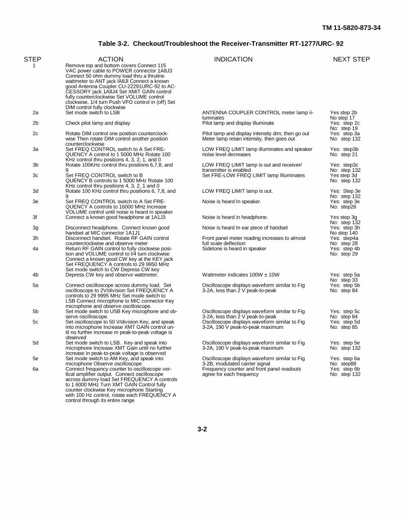
TM 11-5820-873-34
Table 3-2. Checkout/Troubleshoot the Receiver-Transmitter RT-1277/URC- 92
STEP ACTION INDICATION NEXT STEP1 Remove top and bottom covers Connect 115
VAC power cable to POWER connector 1A8J3Connect 50 ohm dummy load thru a thrulinewattmeter to ANT jack lA8Jl Connect a knowngood Antenna Coupler CU-22291URC-92 to AC-CESSORY jack 1A8J4 Set XMIT GAIN controlfully counterclockwise Set VOLUME controlclockwise, 1/4 turn Push VFO control in (off) SetDIM control fully clockwise
2a Set mode switch to LSB ANTENNA COUPLER CONTROL meter lamp ii- Yes step 2bluminates No step 17
2b Check pilot lamp and display Pilot lamp and display illuminate Yes: step 2cNo: step 19
2c Rotate DIM control one position counterclock- Pilot lamp and display intensity dim, then go out Yes: step.3awise Then rotate DIM control another position Meter lamp retain intensity, then goes out No: step 132counterclockwise
3a Set FREQ CONTROL switch to A Set FRE- LOW FREQ LIMIT lamp illuminates and speaker Yes: step3bQUENCY A control to 1 5000 MHz Rotate 100 noise level decreases No: step 21KHz control thru positions 4, 3, 2, 1, and 0
3b Rotate 100KHz control thru positions 6,7,8, and LOW FREQ LIMIT lamp is out and receiver/ Yes: step3c9 transmitter is enabled No: step 132
3c Set FREQ CONTROL switch to B Set FRE-LOW FREQ LIMIT lamp Illuminates Yes step 3dQUENCY B controls to 1 5000 MHz Rotate 100 No: step 132KHz control thru positions 4, 3, 2, 1 and 0
3d Rotate 100 KHz control thru positions 6, 7,8, and LOW FREQ LIMIT lamp is out. Yes: Step 3e9 No: step 132
3e Set FREQ CONTROL switch to A Set FRE- Noise is heard In speaker. Yes: step 3eQUENCY A controls to 16000 MHz Increase No: step26VOLUME control until noise is heard in speaker
3f Connect a known good headphone at 1A1J3 Noise is heard in headphone. Yes step 3gNo: step 132
3g Disconnect headphone. Connect known good Noise is heard In ear piece of handset Yes: step 3hhandset at MIC connector 1A1J1 No step 140
3h Disconnect handset. Rotate RF GAIN control Front panel meter reading increases to almost Yes: step4acounterclockwise and observe meter full scale deflection No: step 28
4a Return RF GAIN control to fully clockwise posi- Sidetone is heard in speaker Yes: step 4btion and VOLUME control to l/4 turn clockwise No: step 29Connect a known good CW key at the KEY jackSet FREQUENCY A controls to 29 9950 MHzSet mode switch to CW Depress CW key
4b Depress CW key and observe wattmeter. Wattmeter indicates 100W ± 10W Yes: step 5aNo: step 33
5a Connect oscilloscope across dummy load. Set Oscilloscope displays waveform similar to Fig Yes: step 5boscilloscope to 2V/division Set FREQUENCY A 3-2A, less than 2 V peak-to-peak No: step 84controls to 29 9995 MHz Set mode switch toLSB Connect microphone to MIC connector Keymicrophone and observe oscilloscope.
5b Set mode switch to USB Key microphone and ob- Oscilloscope displays waveform similar to Fig Yes: step 5cserve oscilloscope. 3-2A, less than 2 V peak-to-peak No: step 84
5c Set oscilloscope to 50 V/division Key, and speak Oscilloscope displays waveform similar to Fig Yes: step 5dinto microphone Increase XMT GAIN control un- 3-2A, 190 V peak-to-peak maximum No: step 85til no further increase m peak-to-peak voltage isobserved
5d Set mode switch to LSB. Key and speak into Oscilloscope displays waveform similar to Fig Yes: step 5emicrophone Increase XMT Gain until no further 3-2A, 190 V peak-to-peak maximum No: step 132increase In peak-to-peak voltage is observed
5e Set mode switch to AM Key, and speak into Oscilloscope displays waveform similar to Fig Yes: step 6amicrophone Observe oscilloscope 3-2B, modulated carrier signal No: step88
6a Connect frequency counter to oscilloscope ver- Frequency counter and front panel readouts Yes: step 6btlcal amplifier output. Connect oscilloscope agree for each frequency No: step 132across dummy load Set FREQUENCY A controlsto 1 6000 MHz Turn XMT GAIN Control fullycounter clockwise Key microphone Startingwith 100 Hz control, rotate each FREQUENCY Acontrol through its entire range
3-2
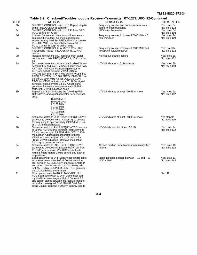
TM 11-5820-873-34Table 3-2. Checkout/Troubleshoot the Receiver-Transmitter RT-1277/URC- 92-Continued
STEP ACTION INDICATION NEXT STEP6b Set FREQ CONTROL switch to B Repeat step 6a Frequency counter and front panel readouts Yes: step 6c
using FREQUENCY B controls agree for each frequency No: step 1326c Set FREQ CONTROL switch to A Pull out VFO VFO lamp illuminates Yes: step 6d
PULL control (VFO on) No: step 1086d Connect frequency counter to oscilloscope ver- Frequency counter indicates 2.0000 MHz ± 5 Yes: step 7a
tlcal amplifier output. Connect oscilloscope KHz minimum No: step 109across dummy load Set FREQUENCY A controlsto 2.0000 MHz Key microphone Rotate VFOPULL Control through its entire range
7a Set FREQ CONTROL to A XMT B RCV. Key Frequency counter indicates 1 6000 MHz and Yes: step7bmicrophone Rotate FREQUENCY B, 10 KHz front panel readouts agree No: step 132control.
7b Release microphone key. Observe front panel No readout change occurs Yes: step 8areadout and rotate FREQUENCY A, 10 KHz con- No: step 132trol
8a Disconnect antenna coupler control cable Discon- VTVM indicates - 10 dB or more Yes: step 8bnect CW key and mlc. Remove dummy load from No: step 110ANT jack IA8JI Connect signal generator toANT jack 1A8J1 Connect VTVM (AC) toPHONE jack 1A1J3 Set mode switch to LSB SetFREQ CONTROL to B Set FREQUENCY B con-trols to 29 9994 MHz Adjust VOLUME CON-TROL for VTVM indication of - 20 dB Set signalgenerator output level to 0.5 uV Adjust signalgenerator frequency to approximately 29 9994MHz, until VTVM indication peaks
8b Repeat step 82 substituting the following FRE- VTVM indicates at least - 10 dB or more Yes: step 9aQUENCY B, and signal generator frequency set- No: step 132tings:
16 0100 MHz10 0100 MHz7 5100 MHz5 0100 MHz3 5100 MHz2.0100 MHz1 6100 MHz
9a Set mode switch to USB Return FREQUENCY B VTVM indicates at least - 10 dB or more Yes step 9bswitches to 29 9994 MHz. Adjust signal genera- No: step 136tor frequency to approximately 29 9994 MHz, un-til VTVM indication peaks.
9b Set mode switch to AM, FREQUENCY B controls VTVM indicates less than - 20 dB Yes: step 9cto 29 9994 MHz Signal generator output level to No: step 1223 0 uV, frequency to 29 9994 MHz, 300k, 1 KHzmodulation Adjust signal generator for peakVTVM indication Adjust VOLUME control for-10 dB VTVM indication. Remove modulationfrom signal generator output.
9c Set mode switch to LSB. Set FREQUENCY B At each position noise blanks momentarily then Yes: step 10switches to 20 000 MHz Disconnect VTVM from returns. No: step 132PHONE jack Increase VOLUME control untilnoise is heard Rotate 1 MHz control thru each ofits positions.
10 Set mode switch to OFF Disconnect control cable Meter indicates a range between + 12 and + 22 Yes: step 11at receiver-transmitter 1A8J4 Connect multim- VDC + 10% No: step 143eter between ACCESSORY connector 1A8J4-Pand ground Set mode switch to AM Slowly ad-just ANTENNA COUPLER CONTROL gam con-trol 1A2R2 thru its entire range.
11 Reset gain control 1A2R2 to 14.5 VDC ± 0.5 Step 12VDC Set mode switch to OFF Disconnect dum-my load from antenna jack 1A&J1 Connect RFand control cables between the receiver-transmit-ter and a known good CU-22291URC-92 An-tenna Coupler Connect a 50 ohm dummy load to
3-3
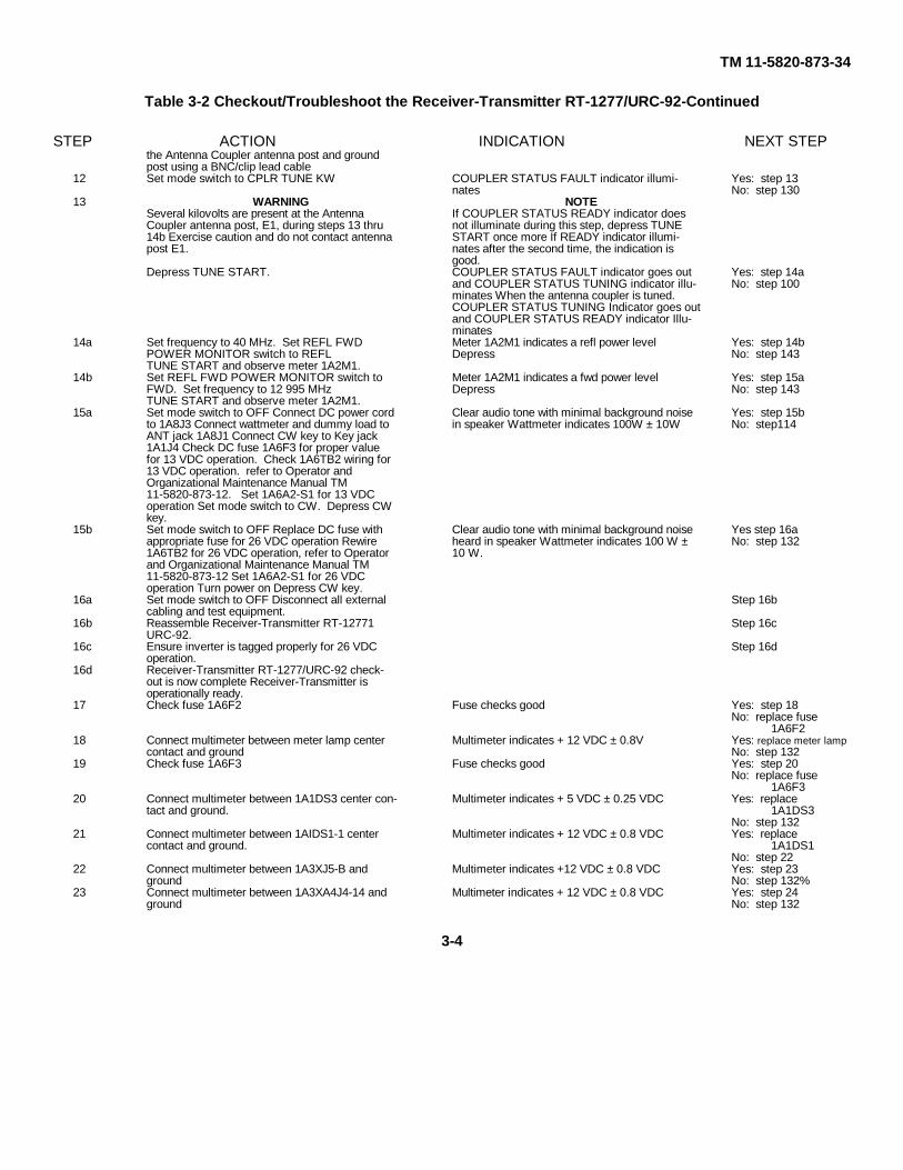
TM 11-5820-873-34
Table 3-2 Checkout/Troubleshoot the Receiver-Transmitter RT-1277/URC-92-Continued
STEP ACTION INDICATION NEXT STEPthe Antenna Coupler antenna post and groundpost using a BNC/clip lead cable
12 Set mode switch to CPLR TUNE KW COUPLER STATUS FAULT indicator illumi- Yes: step 13nates No: step 130
13 WARNING NOTESeveral kilovolts are present at the Antenna If COUPLER STATUS READY indicator doesCoupler antenna post, E1, during steps 13 thru not illuminate during this step, depress TUNE14b Exercise caution and do not contact antenna START once more If READY indicator illumi-post E1. nates after the second time, the indication is
good.Depress TUNE START. COUPLER STATUS FAULT indicator goes out Yes: step 14a
and COUPLER STATUS TUNING indicator illu- No: step 100minates When the antenna coupler is tuned.COUPLER STATUS TUNING Indicator goes outand COUPLER STATUS READY indicator Illu-minates
14a Set frequency to 40 MHz. Set REFL FWD Meter 1A2M1 indicates a refl power level Yes: step 14bPOWER MONITOR switch to REFL Depress No: step 143TUNE START and observe meter 1A2M1.
14b Set REFL FWD POWER MONITOR switch to Meter 1A2M1 indicates a fwd power level Yes: step 15aFWD. Set frequency to 12 995 MHz Depress No: step 143TUNE START and observe meter 1A2M1.
15a Set mode switch to OFF Connect DC power cord Clear audio tone with minimal background noise Yes: step 15bto 1A8J3 Connect wattmeter and dummy load to in speaker Wattmeter indicates 100W ± 10W No: step114ANT jack 1A8J1 Connect CW key to Key jack1A1J4 Check DC fuse 1A6F3 for proper valuefor 13 VDC operation. Check 1A6TB2 wiring for13 VDC operation. refer to Operator andOrganizational Maintenance Manual TM11-5820-873-12. Set 1A6A2-S1 for 13 VDCoperation Set mode switch to CW. Depress CWkey.
15b Set mode switch to OFF Replace DC fuse with Clear audio tone with minimal background noise Yes step 16aappropriate fuse for 26 VDC operation Rewire heard in speaker Wattmeter indicates 100 W ± No: step 1321A6TB2 for 26 VDC operation, refer to Operator 10 W.and Organizational Maintenance Manual TM11-5820-873-12 Set 1A6A2-S1 for 26 VDCoperation Turn power on Depress CW key.
16a Set mode switch to OFF Disconnect all external Step 16bcabling and test equipment.
16b Reassemble Receiver-Transmitter RT-12771 Step 16cURC-92.
16c Ensure inverter is tagged properly for 26 VDC Step 16doperation.
16d Receiver-Transmitter RT-1277/URC-92 check-out is now complete Receiver-Transmitter isoperationally ready.
17 Check fuse 1A6F2 Fuse checks good Yes: step 18No: replace fuse
1A6F218 Connect multimeter between meter lamp center Multimeter indicates + 12 VDC ± 0.8V Yes: replace meter lamp
contact and ground No: step 13219 Check fuse 1A6F3 Fuse checks good Yes: step 20
No: replace fuse1A6F3
20 Connect multimeter between 1A1DS3 center con- Multimeter indicates + 5 VDC ± 0.25 VDC Yes: replacetact and ground. 1A1DS3
No: step 13221 Connect multimeter between 1AIDS1-1 center Multimeter indicates + 12 VDC ± 0.8 VDC Yes: replace
contact and ground. 1A1DS1No: step 22
22 Connect multimeter between 1A3XJ5-B and Multimeter indicates +12 VDC ± 0.8 VDC Yes: step 23ground No: step 132%
23 Connect multimeter between 1A3XA4J4-14 and Multimeter indicates + 12 VDC ± 0.8 VDC Yes: step 24ground No: step 132
3-4
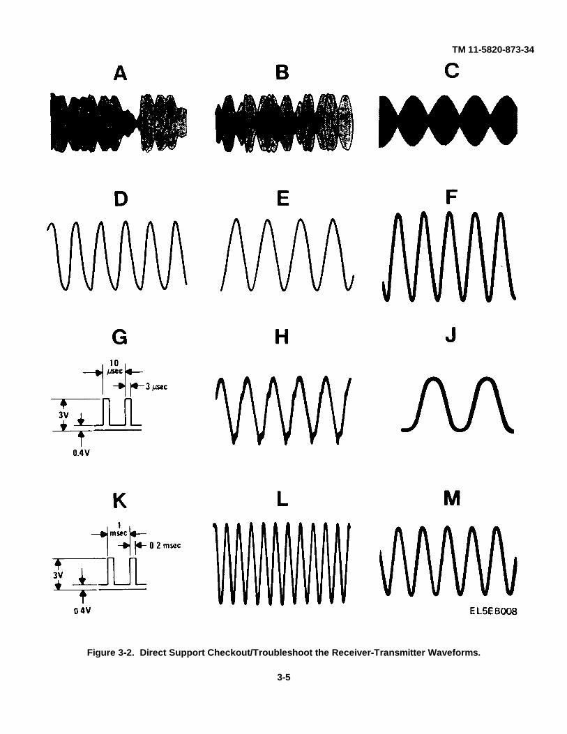
TM 11-5820-873-34
Figure 3-2. Direct Support Checkout/Troubleshoot the Receiver-Transmitter Waveforms.
3-5
TM 11-5820-873-34Table 3-2 Checkout/Troubleshoot the Receiver-Transmitter RT-1277/URC-92-Continued
STEP ACTION INDICATION NEXT STEP24 Connect multimeter between 1A3XA3J3-S and Multimeter indicates + 12 VDC ± 0.8 VDC. Yes: step 25
ground. No: step 13225 Set mode switch to OFF. Replace Audio CCA Receiver-transmitter is disabled. Yes: step 121
1A3A4 with a known good Audio CCA Set mode No: step 134switch to LSB.
26 Connect oscilloscope probe to 1A3XA4J4-18, Check for noise above ambient level. Yes: step 132ground lead to ground. No: step 27
27 Connect multimeter between 1A3XA4J4-14 and Multimeter indicates + 2 VDC to ± 8.0 VDC. Yes: step 133ground. No: step 132
28 Connect multimeter between 1A3XA4J4-15 and Multimeter indicates +2 VDC to +8.0 VDC. Yes: step 132ground. No: step 133
29 Connect frequency counter to 1A3XA3J3-D, Frequency counter indicates 1 KHz. Yes: step 30ground lead to ground Depress CW key. No: step 31
30 Connect frequency counter to 1A3A4P1-4, Frequency counter indicates 1 KHz. Yes: step 133ground lead to ground Depress CW key. No: step 132
31 Continuity check 1AIJ4 center contact to Continuity checks good. Yes step 321AlP2-J. No: step 132
32 Continuity check 1A3XA3J3-2 to 1A3A5-J. Continuity checks good. Yes: step 134No: step 132
33 Connect oscilloscope probe to 1A3XA3J3-16, Oscilloscope displays waveform similar to Fig Yes: step 34ground lead to ground. 3-2C. No: step 37
34 Connect oscilloscope probe to 1A3XA1J1-5, Oscilloscope displays waveform similar to Fig Yes: step 35ground lead to ground Depress CW key. 3-2D. No: step 41
35 Remove 1A3P3 from 1A7J1 Connect VTVM VTVM indicates more than 100 mV. Yes: step 36(AC) to 1A3P3 center contact, ground lead to No: step 42ground Depress CW key.
36 Remove 1A8P3 from 1A7J2 Connect wattmeter Wattmeter indicates more than 90 watts. Yes: step 132to 1A7J2 center contact, ground lead to ground No: step 43Depress CW key.
37 Connect frequency counter to 1A3XA3J3-F, Frequency counter indicates 10.5 MHz. Yes: step 38ground lead to ground Depress CW key. No: step 44
38 Connect multimeter between 1A3XA3J3-T and Multimeter indicates less than + 0.5 VDC. Yes: step 39ground Depress CW key No: step 45
39 Connect multimeter between 1A3XA3J3-S and Multimeter indicates less than + 1.4 VDC. Yes: step40ground Depress CW key No: step 132
40 Connect multimeter between 1A3XA3J3-10 and Multimeter indicates + 12 VDC ± 0.8 VDC. Yes: step 134ground No: step 132
41 Connect oscilloscope probe to 1A3XA2J2-5, Oscilloscope displays waveform similar to Fig Yes: step 132ground lead to ground Depress CW key 3-2D. No: step 46
42 Reconnect 1A7J1 to 1A3P3 Connect VTVM (AC) VTVM indicates more than 100 mV. Yes: step 132to 1A3XA1J1-8, ground lead to ground Depress No: step 49CW key
43 Connect multimeter between 1A7A1J3-F and Multimeter indicates + 28 VDC ± 1.5 VDC. Yes: step 135ground Depress CW key No: step 132
44 Connect VTVM (AC) to 1A4XA1J1-13, ground VTVM indicates 0.1V minimum. Yes: step 132lead to ground Depress CW key No: step 135
45 Connect multimeter between 1A7A1J3-D and Multimeter indicates less than + 0.5 VDC. Yes: step 132ground Depress CW key No: step 135
46 Connect oscilloscope probe to 1A3XA2J2-16, Oscilloscope displays waveform similar to Fig Yes: step 47ground lead to ground Depress CW key 3-2C. No: step 132
47 Connect multimeter between 1A3XA2J2-10 and Multimeter indicates + 12 VDC + 0.8 VDC. Yes: step 48ground Depress CW key No: step 132
48 Connect multimeter between 1A3XA2J2-D and Multimeter indicates + 10 7 VDC ± 0.8 VDC. Yes: step 136ground Depress CW key No: step 59
49 Connect multimeter between 1A3XA1J1-U and Multimeter indicates less than + 1.2 VDC. Yes: step 50ground Depress CW key No: step 61
50 Connect multimeter between 1A3XA1J1-10 and Multimeter indicates + 12 VDC ± 0.8 VDC. Yes: step 51ground No: step 132
51 Connect multimeter between 1A3XA1J1-13 and Multimeter indicates less than + 8 VDC. Yes: step 52ground Depress CW key No: step 62
52 Connect frequency counter to oscilloscope ver- Oscilloscope displays waveform similar to Fig Yes: step 53tlcal output jack Connect oscilloscope probe to 3-2E, minimum amplitude, 300 millivolts Fre- No: step 631A3XA1J1-1, ground lead to ground quency counter indicates 80.75 MHz ± 10 KHz.
3-6
TM 11-5820-873-34Table 3-2 Checkout/Troubleshoot the Receiver-Transmitter RT-1277/URC-92-Continued
STEP ACTION INDICATION NEXT STEP
53 Connect oscilloscope with frequency counter at Frequency counter indicates between 111.000 Yes: step 137vertical output to 1A3XA1J1-18, ground lead to MHz and 122.000 MHz. No: step 64ground.
54 Connect frequency counter to oscilloscope Oscilloscope displays waveform similar to Fig Yes: step138vertical output jack Connect oscilloscope probe 3-2F, 0 3 to 0 9 V peak-to-peak Frequency coun- No: step 132to 1A4XA1J1-S, ground lead to ground. ter indicates 5 0 MHz ± 5 Hz.
55 Connect multimeter between 1A4A6-E1 and Multimeter indicates + 12 VDC ± 0.8 VDC. Yes: step56ground. No: step 132
56 Connect multimeter between 1A4A6XALJ1-K Multimeter indicates + 12 VDC ± 0.8 VDC. Yes: step 57and ground. No: step 132
57 Connect multimeter between 1A6A1-15 and Multimeter indicates + 5 VDC ± 0.25 VDC. Yes: step 138ground. No: step 58
58 Check fuse 1A6A1F3. Fuse checks good. Yes: step 132No: replace fuse
1A6A1F3 If fuseblows again goto step 120
59 Connect multimeter between 1A3A5-R and Multimeter indicates + 12 VDC ± 0.8 VDC. Yes: step 60ground. No: step 132
60 Connect multimeter between 1A3A5XA2J2-8 Multimeter indicates + 12 VDC ± 0.8 VDC. Yes: step 136and ground. No: step 132
61 Connect multimeter between 1A7A1J3-B and Multimeter indicates less than +1.2VDC. Yes: step 132ground Depress CW key. No: step 135
62 Connect multimeter between 1A3XA2J2-P and Multimeter indicates less than + 8.0 VDC. Yes: step 132ground Depress CW key. No: step 136
63 Connect oscilloscope probe to 1A4XA3J3-11, Oscilloscope displays waveform similar to Fig Yes: step 132ground lead to ground. 3-2E. minimum amplitude 300 millivolts Fre- No: step 65
quency counter indicates 80.75 MHz ± 10 KHz.64 Remove 1A3P1 from 1A4A5-J1. Connect fre- Frequency counter indicates between 111.0000 Yes: step 132
quency counter to oscilloscope vertical output MHz and 122.0000MHz. No: step69Connect oscilloscope probe to 1A4A5-J1 centerpin, ground lead to ground
65 Connect RF voltmeter to 1A4XA3J3-D, ground RF voltmeter indicates .085 V minimum. Yes: step 66lead to ground. No: step 70
66 Connect frequency counter to oscilloscope ver- Oscilloscope displays waveform similar to Fig Yes: step 67tlcal output jack Connect oscilloscope probe to 3-2G, 0 3 V minimum amplitude. Frequency No: step 711A4XA3J3-P, ground lead to ground. counter indicates 20 MHz + 20 Hz.
67 Connect frequency counter to 1A4XA3J3-B Frequency counter indicates between 1.5000 Yes: step 68ground lead to ground. MHz and 1.5999 MHz. No: step 72
68 Connect frequency counter to 1A4XA3J3-U, Frequency counter indicates between 111.0000 Yes step 139ground lead to ground. MHz and 122.0000 MHz. No: step 73
69 Connect multimeter between 1A4XA5J5-4 and Multimeter indicates + 2.0 VDC ± 0.5 VDC . Yes: step 140ground. No: step 74
70 Connect RF voltmeter to 1A4XA1J1-4, ground RF voltmeter indicates .085 V minimum. Yes: step 132lead to ground. No: step 138
71 Connect oscilloscope probe to 1A4XAIJl-1, Oscilloscope displays waveform similar to Fig Yes: step 132ground lead to ground. 3-2G, 0 3 V minimum amplitude Frequency No: step 138
counter indicates 20 MHz ± 20 Hz.72 Connect frequency counter to 1A4XA2J2-1, Frequency counter indicates between 1.5000 Yes: step 132
ground lead to ground. MHz and 1.5999 MHz No: step 7573 Connect frequency counter to 1A4XA5J5-2, Frequency counter indicates between 111.0000 Yes: step 132
ground lead to ground. MHz and 122.0000 MHz No: step 14074 Connect multimeter between 1A4XA4J4-15 and Multimeter indicates + 2.0 VDC ± 0.5 VDC Yes: step 132
ground. No: step 7875 Connect frequency counter to oscilloscope ver- Oscilloscope displays waveform similar to Fig Yes: step 76
tical output jack Connect oscilloscope probe to 3-2H. Frequency counter indicates 1 KHz ± 1 No: step 801A4XA2J2-18, ground lead to ground Hz.
76 Connect VTVM (AC) to 1A4XA2J2-C, ground VTVM indicates .09 V peak-to-peak minimum Yes: step 77lead to ground. No: step 81
77 Connect multimeter between 1A4XA2J2-U and Multimeter indicates + 7.7 VDC ± 0.8 VDC Yes: step 141ground. No: step 132
78 Set FREQUENCY A controls to 00.0000 MHz Oscilloscope displays waveform similar to Fig Yes: step79Connect oscilloscope probe to 1A4XA4J4-V, 3-2J. No: step82Ground lead to ground
3-7
TM 11-5820-873-34
Table 3-2 Checkout/Troubleshoot the Receiver-Transmitter RT-1277/URC-92-ContinuedSTEP ACTION INDICATION NEXT STEP
79 Connect oscilloscope to 1A4XA4J4-B, ground Oscilloscope displays waveform similar to Fig Yes: step 142lead to ground. 3-2K. No: step 83
80 Connect oscilloscope probe to 1A4XA1J1-18, Oscilloscope displays waveform similar to Fig Yes: step 132ground to lead ground. 3-2H. No: step 138
81 Connect VTVM (ACO 1A4XA1J1-6, ground lead VTVM indicates 09 V peak-to-peak minimum. Yes step 132to ground. No: step 138
82 Connect oscilloscope probe to 1A4XA1J1-17, Oscilloscope displays waveform similar to Fig Yes: step132ground lead to ground. 3-2J. No: step 138
83 Connect oscilloscope to 1A4XA3J3-15, ground Oscilloscope displays waveform similar to Fig Yes: step 132lead to ground. 3-2L. No: step 139
84 Replace Sideband Generator CCA with known Oscilloscope displays waveform similar to Fig Yes: step 134good Sideband Generator CCA Key microphone. 3-2A, less than 2 V peak-to-peak maximum. No: step 132
85 Connect multimeter between 1A3XA3J3-17 and Multimeter indicates less than +1.6VDC. Yes: step 86ground. No: step 132
86 Connect frequency counter to 1A3XA2J2-1. Frequency counter indicates 10.5 MHz. Yes: step 136No: step 87
87 Connect frequency counter to 1A3XA3J3- 1. Frequency counter indicates 10.5 MHz. Yes: step 132No: step 134
88 Connect multimeter between 1A3A5-E11 and Multimeter indicates + 12 VDC ± 0.8 VDC. Yes: step 89ground. No: step 132
89 Connect multimeter between 1A3A5XA2J2-6 Multimeter indicates + 12 VDC ± 0.8 VDC. Yes: step 90and ground. No: step 132
90 Connect multimeter between 1A3A5XA3J3-5 Multimeter indicates + 12 VDC ± 0.8 VDC. Yes: step 91and ground. No: step 132
91 Connect frequency counter to 1A3A5XA2J2-1, Frequency counter indicates 10.5 MHz. Yes: step 136ground lead to ground. No: step 134
92 Remove Translator CCA 1A4A3 Connect fre- Frequency checks are correct. Yes: step 93quency counter to 1A4XA2J2-1. Perform fre- No: step 97quency checks as shown below.
Frequency ChecksFrequency Switch Settings
10 KHz 1 KHz 100 Hz FREQUENCY0 0 1 1.5001 MHz0 0 2 1.5002 MHz0 0 3 1.5003 MHz0 0 4 1.5004 MHz0 0 5 1.5005 MHz0 0 6 1.5006 MHz0 0 7 1.5007 MHz0 0 8 1.5008 MHz0 0 9 1.5009MHz
10 KHz 1 KHz 100 Hz FREQUENCY0 1 0 1.5010 MHz0 2 0 1.5020 MHz0 3 0 1.5030 MHz0 4 0 1.5040 MHz0 5 0 1.5050 MHz0 6 0 1.5060 MHz0 7 0 1.5070 MHz0 8 0 1.5080 MHz0 9 0 1.5090 MHz
10 KHz 1 KHz 100 Hz FREQUENCY1 0 0 1.5100 MHz2 0 0 1.5200 MHz3 0 0 1.5300 MHz4 0 0 1.5400 MHz5 0 0 1.5500 MHz6 0 0 1.5600 MHz7 0 0 1.5700 MHz8 0 0 1.5800 MHz9 0 0 1.5900 MHz
3-8
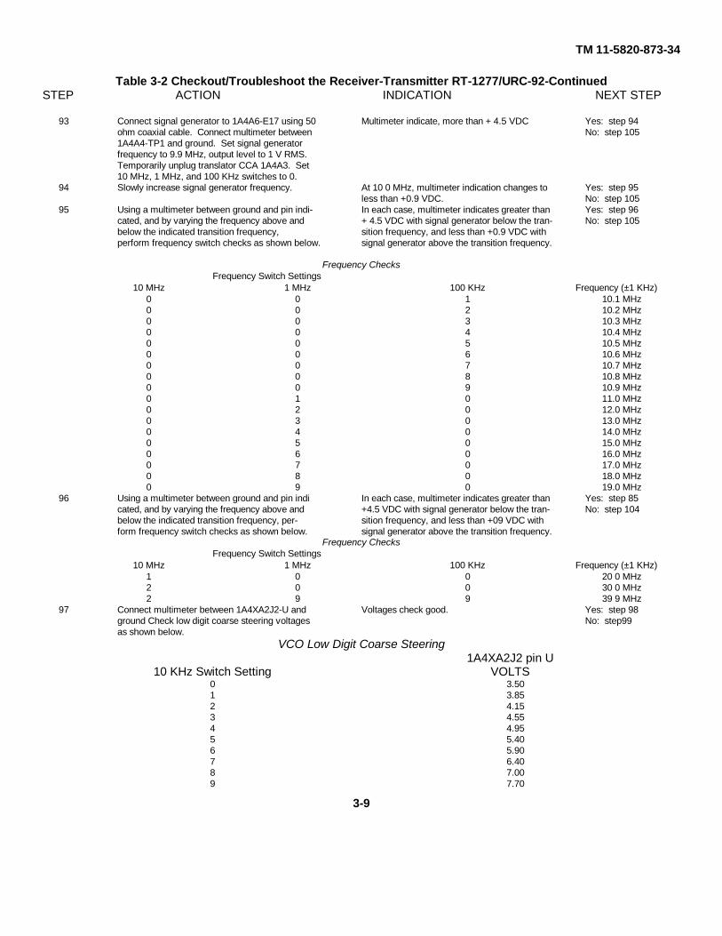
TM 11-5820-873-34
Table 3-2 Checkout/Troubleshoot the Receiver-Transmitter RT-1277/URC-92-ContinuedSTEP ACTION INDICATION NEXT STEP
93 Connect signal generator to 1A4A6-E17 using 50 Multimeter indicate, more than + 4.5 VDC Yes: step 94ohm coaxial cable. Connect multimeter between No: step 1051A4A4-TP1 and ground. Set signal generatorfrequency to 9.9 MHz, output level to 1 V RMS.Temporarily unplug translator CCA 1A4A3. Set10 MHz, 1 MHz, and 100 KHz switches to 0.
94 Slowly increase signal generator frequency. At 10 0 MHz, multimeter indication changes to Yes: step 95less than +0.9 VDC. No: step 105
95 Using a multimeter between ground and pin indi- In each case, multimeter indicates greater than Yes: step 96cated, and by varying the frequency above and + 4.5 VDC with signal generator below the tran- No: step 105below the indicated transition frequency, sition frequency, and less than +0.9 VDC withperform frequency switch checks as shown below. signal generator above the transition frequency.
Frequency ChecksFrequency Switch Settings
10 MHz 1 MHz 100 KHz Frequency (±1 KHz)0 0 1 10.1 MHz0 0 2 10.2 MHz0 0 3 10.3 MHz0 0 4 10.4 MHz0 0 5 10.5 MHz0 0 6 10.6 MHz0 0 7 10.7 MHz0 0 8 10.8 MHz0 0 9 10.9 MHz0 1 0 11.0 MHz0 2 0 12.0 MHz0 3 0 13.0 MHz0 4 0 14.0 MHz0 5 0 15.0 MHz0 6 0 16.0 MHz0 7 0 17.0 MHz0 8 0 18.0 MHz0 9 0 19.0 MHz
96 Using a multimeter between ground and pin indi In each case, multimeter indicates greater than Yes: step 85cated, and by varying the frequency above and +4.5 VDC with signal generator below the tran- No: step 104below the indicated transition frequency, per- sition frequency, and less than +09 VDC withform frequency switch checks as shown below. signal generator above the transition frequency.
Frequency ChecksFrequency Switch Settings
10 MHz 1 MHz 100 KHz Frequency (±1 KHz)1 0 0 20 0 MHz2 0 0 30 0 MHz2 9 9 39 9 MHz
97 Connect multimeter between 1A4XA2J2-U and Voltages check good. Yes: step 98ground Check low digit coarse steering voltages No: step99as shown below.
VCO Low Digit Coarse Steering1A4XA2J2 pin U
10 KHz Switch Setting VOLTS0 3.501 3.852 4.153 4.554 4.955 5.406 5.907 6.408 7.009 7.70
3-9
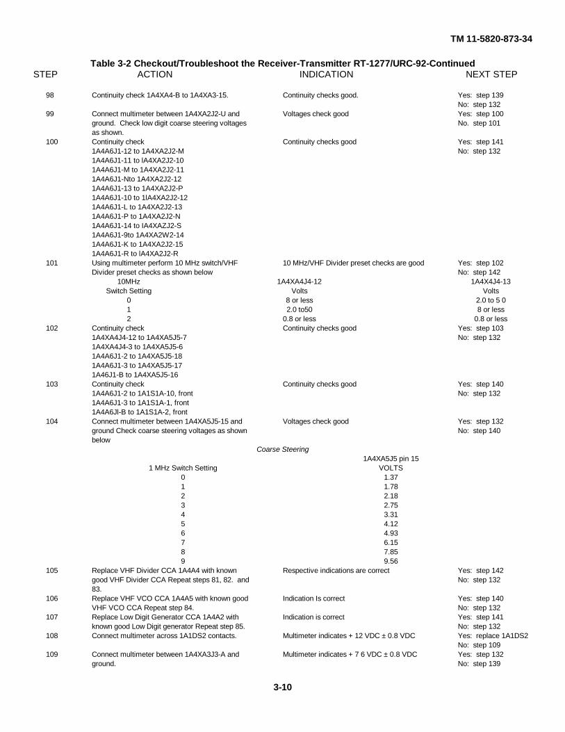
TM 11-5820-873-34
Table 3-2 Checkout/Troubleshoot the Receiver-Transmitter RT-1277/URC-92-ContinuedSTEP ACTION INDICATION NEXT STEP
98 Continuity check 1A4XA4-B to 1A4XA3-15. Continuity checks good. Yes: step 139No: step 132
99 Connect multimeter between 1A4XA2J2-U and Voltages check good Yes: step 100ground. Check low digit coarse steering voltages No. step 101as shown.
100 Continuity check Continuity checks good Yes: step 1411A4A6J1-12 to 1A4XA2J2-M No: step 1321A4A6J1-11 to lA4XA2J2-101A4A6J1-M to 1A4XA2J2-111A4A6J1-Nto 1A4XA2J2-121A4A6J1-13 to 1A4XA2J2-P1A4A6J1-10 to 1lA4XA2J2-121A4A6J1-L to 1A4XA2J2-131A4A6J1-P to 1A4XA2J2-N1A4A6J1-14 to IA4XAZJ2-S1A4A6J1-9to 1A4XA2W2-141A4A6J1-K to 1A4XA2J2-151A4A6J1-R to lA4XA2J2-R
101 Using multimeter perform 10 MHz switch/VHF 10 MHz/VHF Divider preset checks are good Yes: step 102Divider preset checks as shown below No: step 142
10MHz 1A4XA4J4-12 1A4X4J4-13Switch Setting Volts Volts
0 8 or less 2.0 to 5 01 2.0 to50 8 or less2 0.8 or less 0.8 or less
102 Continuity check Continuity checks good Yes: step 1031A4XA4J4-12 to 1A4XA5J5-7 No: step 1321A4XA4J4-3 to 1A4XA5J5-61A4A6J1-2 to 1A4XA5J5-181A4A6J1-3 to 1A4XA5J5-171A46J1-B to 1A4XA5J5-16
103 Continuity check Continuity checks good Yes: step 1401A4A6J1-2 to 1A1S1A-10, front No: step 1321A4A6J1-3 to 1A1S1A-1, front1A4A6Jl-B to 1A1S1A-2, front
104 Connect multimeter between 1A4XA5J5-15 and Voltages check good Yes: step 132ground Check coarse steering voltages as shown No: step 140below
Coarse Steering1A4XA5J5 pin 15
1 MHz Switch Setting VOLTS0 1.371 1.782 2.183 2.754 3.315 4.126 4.937 6.158 7.859 9.56
105 Replace VHF Divider CCA 1A4A4 with known Respective indications are correct Yes: step 142good VHF Divider CCA Repeat steps 81, 82. and No: step 13283.
106 Replace VHF VCO CCA 1A4A5 with known good Indication Is correct Yes: step 140VHF VCO CCA Repeat step 84. No: step 132
107 Replace Low Digit Generator CCA 1A4A2 with Indication is correct Yes: step 141known good Low Digit generator Repeat step 85. No: step 132
108 Connect multimeter across 1A1DS2 contacts. Multimeter indicates + 12 VDC ± 0.8 VDC Yes: replace 1A1DS2No: step 109
109 Connect multimeter between 1A4XA3J3-A and Multimeter indicates + 7 6 VDC ± 0.8 VDC Yes: step 132ground. No: step 139
3-10
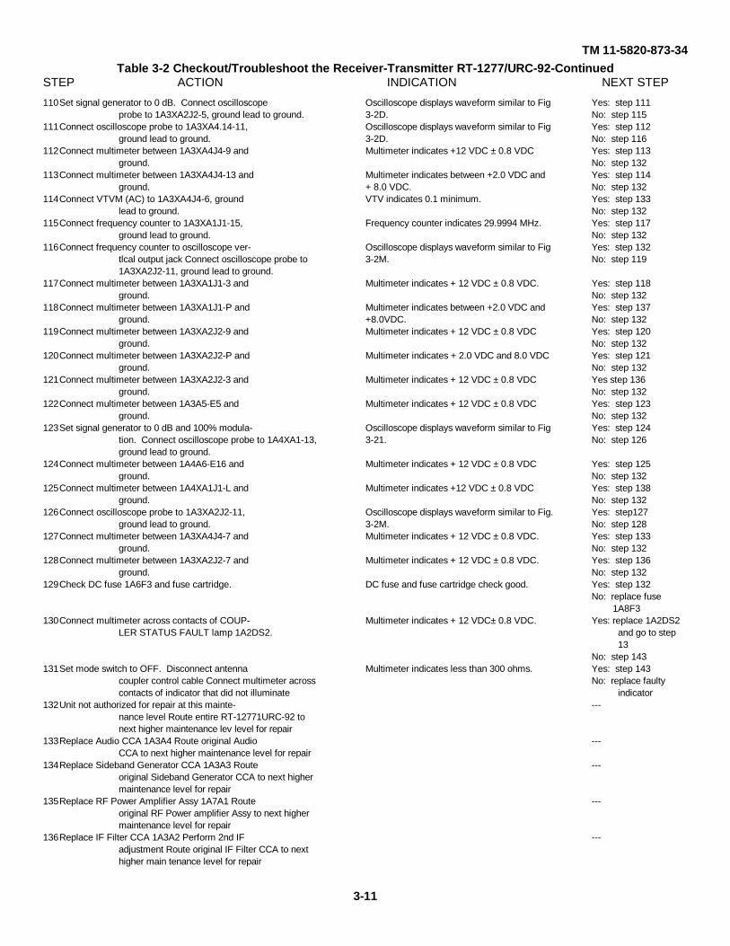
TM 11-5820-873-34Table 3-2 Checkout/Troubleshoot the Receiver-Transmitter RT-1277/URC-92-Continued
STEP ACTION INDICATION NEXT STEP
110Set signal generator to 0 dB. Connect oscilloscope Oscilloscope displays waveform similar to Fig Yes: step 111probe to 1A3XA2J2-5, ground lead to ground. 3-2D. No: step 115
111Connect oscilloscope probe to 1A3XA4.14-11, Oscilloscope displays waveform similar to Fig Yes: step 112ground lead to ground. 3-2D. No: step 116
112Connect multimeter between 1A3XA4J4-9 and Multimeter indicates +12 VDC ± 0.8 VDC Yes: step 113ground. No: step 132
113Connect multimeter between 1A3XA4J4-13 and Multimeter indicates between +2.0 VDC and Yes: step 114ground. + 8.0 VDC. No: step 132
114Connect VTVM (AC) to 1A3XA4J4-6, ground VTV indicates 0.1 minimum. Yes: step 133lead to ground. No: step 132
115Connect frequency counter to 1A3XA1J1-15, Frequency counter indicates 29.9994 MHz. Yes: step 117ground lead to ground. No: step 132
116Connect frequency counter to oscilloscope ver- Oscilloscope displays waveform similar to Fig Yes: step 132tlcal output jack Connect oscilloscope probe to 3-2M. No: step 1191A3XA2J2-11, ground lead to ground.
117Connect multimeter between 1A3XA1J1-3 and Multimeter indicates + 12 VDC ± 0.8 VDC. Yes: step 118ground. No: step 132
118Connect multimeter between 1A3XA1J1-P and Multimeter indicates between +2.0 VDC and Yes: step 137ground. +8.0VDC. No: step 132
119Connect multimeter between 1A3XA2J2-9 and Multimeter indicates + 12 VDC ± 0.8 VDC Yes: step 120ground. No: step 132
120Connect multimeter between 1A3XA2J2-P and Multimeter indicates + 2.0 VDC and 8.0 VDC Yes: step 121ground. No: step 132
121Connect multimeter between 1A3XA2J2-3 and Multimeter indicates + 12 VDC ± 0.8 VDC Yes step 136ground. No: step 132
122Connect multimeter between 1A3A5-E5 and Multimeter indicates + 12 VDC ± 0.8 VDC Yes: step 123ground. No: step 132
123Set signal generator to 0 dB and 100% modula- Oscilloscope displays waveform similar to Fig Yes: step 124tion. Connect oscilloscope probe to 1A4XA1-13, 3-21. No: step 126ground lead to ground.
124Connect multimeter between 1A4A6-E16 and Multimeter indicates + 12 VDC ± 0.8 VDC Yes: step 125ground. No: step 132
125Connect multimeter between 1A4XA1J1-L and Multimeter indicates +12 VDC ± 0.8 VDC Yes: step 138ground. No: step 132
126Connect oscilloscope probe to 1A3XA2J2-11, Oscilloscope displays waveform similar to Fig. Yes: step127ground lead to ground. 3-2M. No: step 128
127Connect multimeter between 1A3XA4J4-7 and Multimeter indicates + 12 VDC ± 0.8 VDC. Yes: step 133ground. No: step 132
128Connect multimeter between 1A3XA2J2-7 and Multimeter indicates + 12 VDC ± 0.8 VDC. Yes: step 136ground. No: step 132
129Check DC fuse 1A6F3 and fuse cartridge. DC fuse and fuse cartridge check good. Yes: step 132No: replace fuse
1A8F3130Connect multimeter across contacts of COUP- Multimeter indicates + 12 VDC± 0.8 VDC. Yes: replace 1A2DS2
LER STATUS FAULT lamp 1A2DS2. and go to step13
No: step 143131Set mode switch to OFF. Disconnect antenna Multimeter indicates less than 300 ohms. Yes: step 143
coupler control cable Connect multimeter across No: replace faultycontacts of indicator that did not illuminate indicator
132Unit not authorized for repair at this mainte- ---nance level Route entire RT-12771URC-92 tonext higher maintenance lev level for repair
133Replace Audio CCA 1A3A4 Route original Audio ---CCA to next higher maintenance level for repair
134Replace Sideband Generator CCA 1A3A3 Route ---original Sideband Generator CCA to next highermaintenance level for repair
135Replace RF Power Amplifier Assy 1A7A1 Route ---original RF Power amplifier Assy to next highermaintenance level for repair
136Replace IF Filter CCA 1A3A2 Perform 2nd IF ---adjustment Route original IF Filter CCA to nexthigher main tenance level for repair
3-11
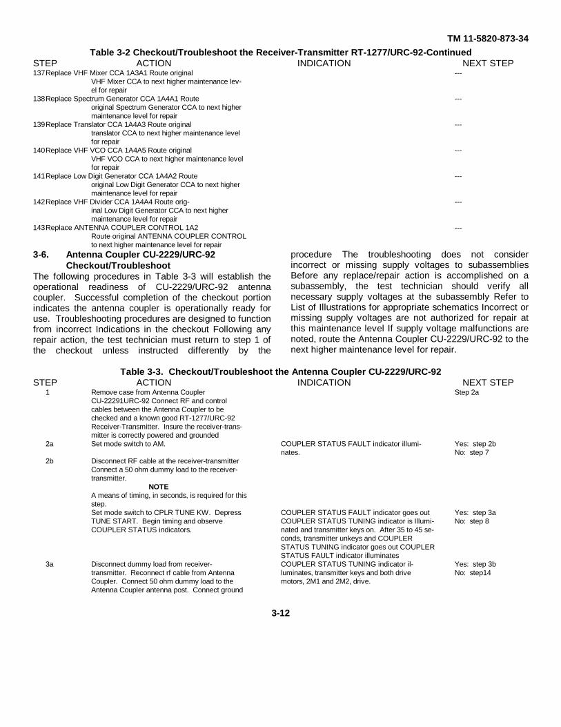
TM 11-5820-873-34Table 3-2 Checkout/Troubleshoot the Receiver-Transmitter RT-1277/URC-92-Continued
STEP ACTION INDICATION NEXT STEP137Replace VHF Mixer CCA 1A3A1 Route original ---
VHF Mixer CCA to next higher maintenance lev-el for repair
138Replace Spectrum Generator CCA 1A4A1 Route ---original Spectrum Generator CCA to next highermaintenance level for repair
139Replace Translator CCA 1A4A3 Route original ---translator CCA to next higher maintenance levelfor repair
140Replace VHF VCO CCA 1A4A5 Route original ---VHF VCO CCA to next higher maintenance levelfor repair
141Replace Low Digit Generator CCA 1A4A2 Route ---original Low Digit Generator CCA to next highermaintenance level for repair
142Replace VHF Divider CCA 1A4A4 Route orig- ---inal Low Digit Generator CCA to next highermaintenance level for repair
143Replace ANTENNA COUPLER CONTROL 1A2 ---Route original ANTENNA COUPLER CONTROLto next higher maintenance level for repair
3-6. Antenna Coupler CU-2229/URC-92Checkout/Troubleshoot
The following procedures in Table 3-3 will establish theoperational readiness of CU-2229/URC-92 antennacoupler. Successful completion of the checkout portionindicates the antenna coupler is operationally ready foruse. Troubleshooting procedures are designed to functionfrom incorrect Indications in the checkout Following anyrepair action, the test technician must return to step 1 ofthe checkout unless instructed differently by the
procedure The troubleshooting does not considerincorrect or missing supply voltages to subassembliesBefore any replace/repair action is accomplished on asubassembly, the test technician should verify allnecessary supply voltages at the subassembly Refer toList of Illustrations for appropriate schematics Incorrect ormissing supply voltages are not authorized for repair atthis maintenance level If supply voltage malfunctions arenoted, route the Antenna Coupler CU-2229/URC-92 to thenext higher maintenance level for repair.
Table 3-3. Checkout/Troubleshoot the Antenna Coupler CU-2229/URC-92STEP ACTION INDICATION NEXT STEP
1 Remove case from Antenna Coupler Step 2aCU-22291URC-92 Connect RF and controlcables between the Antenna Coupler to bechecked and a known good RT-1277/URC-92Receiver-Transmitter. Insure the receiver-trans-mitter is correctly powered and grounded
2a Set mode switch to AM. COUPLER STATUS FAULT indicator illumi- Yes: step 2bnates. No: step 7
2b Disconnect RF cable at the receiver-transmitterConnect a 50 ohm dummy load to the receiver-transmitter.
NOTEA means of timing, in seconds, is required for thisstep.Set mode switch to CPLR TUNE KW. Depress COUPLER STATUS FAULT indicator goes out Yes: step 3aTUNE START. Begin timing and observe COUPLER STATUS TUNING indicator is Illumi- No: step 8COUPLER STATUS indicators. nated and transmitter keys on. After 35 to 45 se-
conds, transmitter unkeys and COUPLERSTATUS TUNING indicator goes out COUPLERSTATUS FAULT indicator illuminates
3a Disconnect dummy load from receiver- COUPLER STATUS TUNING indicator il- Yes: step 3btransmitter. Reconnect rf cable from Antenna luminates, transmitter keys and both drive No: step14Coupler. Connect 50 ohm dummy load to the motors, 2M1 and 2M2, drive.Antenna Coupler antenna post. Connect ground
3-12
TM 11-5820-873-34Table 3-3. Checkout/Troubleshoot the Antenna Coupler CU-2229/URC-92-Continued
STEP ACTION INDICATION NEXT STEP
to ground post. Set frequency to 1 602 MHz.Depress TUNE START.
3b Set mode selector to CW. COUPLER STATUS FAULT indicator Is Illumi- Yes: step 4anated, transmitter unkeys and drive motors stop No: step33driving.
4a Set mode switch to CPI,R TUNE KW. Depress NOTETUNESTART. If the time delay runs out during this test, de-
press TUNE START once more If tuning occursthe second tune the indication is goodAntenna Coupler completes tune cycle, Yes: step 4bCOUPLER STATUS FAUI,T indicator goes out No: step 34and COUPLER STATUS READY indicatorilluminates.
4b Set mode switch to CW then return to CPLR COUPLER STATUS READY indicator goes out Yes: step 4cTUNE KW. And COUPLER STATUS FAULT indicator No: step 35
illuminates.4c Set mode switch to AM Key transmitter. COUPLER STATUS FAULT indicator goes out Yes: step 4d
and COUPLER STATUS READY indicator No: step 37illuminates.
4d Set frequency to 1 802 MHz Key transmitter. COUPLER STATUS FAULT indicator Yes: step 4eilluminates. No: step 37
4e Set frequency to l 602 MHz Key transmitter COUPLER STATUS READY indicator Yes: step 5ailluminates. No: step 37
5a Perform the following procedure for each setting NOTE Yes: step 6alisted Set and tune to the tune frequency Reset The Antenna Coupler Control gain adjustment No: step39frequency to the check frequency. Set mode can affect both the REFL power indication andswitch to CW and key transmitter Check both tuning Normal gain setting is about 14.5 VDC ±the FWD and REFL power. 0.5 VDC but a sight adjustment may be neces-
NOTE sary If some frequencies do not tune, adjust theThe frequencies below do not necessarily match gain slightly clockwise If the REFL power indi-the average powers listed in the Indication cation is a little high, adjust the gain slightlycolumn for this step. counterclockwise The final gain control setting
Tune Check must satisfy both requirements If not, proceed toFrequency Frequency the troubleshooting reference for this step
1.604 1.602 Antenna coupler completes each tune cycle Also2.004 2.002 the power readings should be approximate to one4.001 4.000 of the acceptable FWDIREFL ratios below8.001 8.000 Average REFL12.001 12.000 FWD (watts) (or less)16.001 16.001 20 0.820.001 20.000 30 1.224.001 24.000 40 1 629.999 29.998 50 2.0
60 2.470 2.880 3.2100 4.0
6a Set mode switch to OFF Disconnect cabling be-tween receiver-transmitter and coupler unit.
6b Reassemble Antenna Coupler Unit6c Antenna Coupler Unit CU-22291URC-92 check-
out is now complete. Coupler unit is now service-able.
7 Set mode switch to OFF Remove Control Logic COUPLER STATUS FAULT indicator Yes: step 37CCA 2A1. Set mode switch to AM. Jumper illuminates. No: step392XA1-12 to ground.
8 COUPLER STATUS FAULT indicator went out. Yes: step 9No: step 10
9 COUPLER STATUS TUNING indicator Illumi- Yes: step37nated and transmitter is keyed No: step 11
10 Set mode switch to OFF Remove Control Logic COUPLER STATUS FAULT indicator is not lit Yes: step37CCA 2A1 Set mode switch to CPLR TUNE KW. No: step 39
11 COUPLER STATUS TUNING indicator Yes: step 12illuminated No: step 13
3-13
TM 11-5820-873-34Table 3-3. Checkout/Troubleshoot the Antenna Coupler CU-2229/URC-92-Continued
STEP ACTION INDICATION NEXT STEP12 Set mode switch to OFF Remove Control Logic
CCA 2A1 Set mode switch to AMCAUTION
When testing on or jumpering connector con-tacts, take care not to short adjacent contactJumper 2XA1-7 to ground Transmitter keys on Yes: step 37
No: step3913 Set mode switch to OFF Remove Control Logic
CCA 2A1 Set mode switch to CPLR TUNE KWCAUTION
When testing on or jumpering connector con-tacts, take care not to short adjacent contactsJumper2XAl-6toground COUPLER STATUS TUNING indicator Yes: step37
Illuminates. No: step 3914 Set frequency to 1.802 MHz. Depress TUNE Both drive motors, 2M1 and 2M2, drive. Yes: step 3b
START No: step 1l15 Drive motor 2M1 drives. Yes: step 16
No: step 2316 Set mode switch to OFF. Remove Phase and
Amplitude CCA 2A2CAUTION
When testing on or jumpering connector con-tacts, take care not to short adjacent contacts
CAUTIONInsure roller on 2L4 is positioned near center oftravel before beginning the following checks
NOTEFor steps requiring jumpers, remove jumper be-fore motor drives to end stepSet mode switch to AM. Momentarily jumper Motor 2M2 rotates clockwise (viewed from shaft Yes: step 172XA2-V to ground. end). No: step 39
17 Momentarily jumper 2XA2-17 to ground Motor 2M2 rotates counterclockwise Yes step 18No: step 39
18 Connect VTVM between 2XA2-U and ground Meter indicates + 10 VDC + 0.8 VDC Yes step 19No: step 39
19 CAUTIONEnsure VTVM is isolated from groundConnect VTVM between 2XA2-16 and 2XA2-U Meter indicates a voltage difference(+ or -) Yes: step 20
No: step 3920 Set mode switch to CPLR TUNE KW Connect Meter indicates + 3 VDC to + 5 VDC Yes: step 21
VTVM between 2XA2-14 and ground. Depress No: step 39and hold TUNE START
21 Set mode switch to OFF. Connect multimeter Meter indicates 200 ohms or more Yes: step 22between 2XA2-7 and ground No: step 39
22 Connect multimeter between 2XA2-15 and Meter indicates 1000 ohms or more Yes: step 35ground No: step 39
23 Drive motor 2M2 drives Yes: step 24No: step 30
24 Set mode switch to OFF. Remove Phase andAmplitude CCA 2A2
CAUTIONWhen testing on or jumpering connector con-tacts, take care not to short adjacent contactsEnsure the 2C1 sensor bar is positioned near cen-ter of travel before beginning the followingchecks
NOTEFor steps requiring jumpers, remove jumperbefore sensor contacts micro switchesSet mode switch to AM. Momentarily jumper Motor 2M1 rotates clockwise (viewed from shaft Yes: step 252XA2-4 to ground end) No: step 39
25 Momentarily jumper 2XA2-5 to ground Motor 2M 1 rotates counterclockwise Yes: step 26No: step 39
26 Connect VTVM between 2XA2-3 and ground Meter indicates + 10 VDC + 0.8 VDC Yes step 27No: step 39
3-14
TM 11-5820-873-34
Table 3-3. Checkout/Troubleshoot the Antenna Coupler CU-2229/URC-92-ContinuedSTEP ACTION INDICATION NEXT STEP
27 CAUTIONEnsure VTVM is Isolated from groundConnect VTVM between 2XA2-2 and 2XA2-3 Meter indicates a voltage difference(+ or -) Yes: step 28
No: step 3928 Set mode switch to OFF. Connect multimeter Meter indicates 1000 ohms or more. Yes step 29
between 2XA2-8 and ground. No: step 3929 Connect multimeter between 2XA2-11 and Meter indicates 1000 ohms or more Yes: step 38
ground. No step 3930 Set mode switch to OFF Remove Control Logic Meter indicates greater than 0.1 VDC Yes step 31
CCA 2A1. Set mode switch to AM. Connect No: step 39VTVM between 2XA1-3 and 2XA 1-F
31 Connect VTVM between 2XA1-B and ground Meter indicates + 12 VDC ± 4 VDC Yes step 32No: step 39
32 Set mode switch to OFF Reinstall Control Logic Meter indicates 0 VDC ± 0.5 VDC Yes step 38CCA 2A2 Remove Phase and Amplitude Control No: Reinstall PhaseCCA 2A2 Set mode switch to CPLR TUNE KW. and AmplitudeConnect VTVM between 2XA2- 10 and ground. Control CCA
33 Set mode switch to OFF Remove Control Logic 2A2, go toCCA 2A1 Set mode switch to CPL,RTUNE KW step 37
CAUTIONWhen testing on or jumpering connector con-tacts, take care not to short adjacent contactsConnect VTVM between 2XA1-2 and ground Meter indicates + 10 VDC ± 0. 8 VDC Yes step 37
No: step 3934 Set mode switch to OFF Replace Control Logic NOTE
CCA 2A1 with a known good Control Logic CCA If the time delay runs out during this test, de-Set mode switch to CPLR TUNE KW Depress press TUNE START once more If tuningTUNE START. occurs the second time, the indication is good
Antenna Coupler completes tune cycle, Yes step 37COUPLER STATUS FAULT indicator goes out No: step 39and COUPLER STATUS READY illuminates.
35 Set mode switch to OFF Replace Control Logic COUPLER STATUS READY indicator goes out Yes step 37CCA 2A1 with a known good Control Logic CCA and COUPLER STATUS FAULT indicator No: step39Set mode switch to CPLR TUNE KW. Depress illuminates.TUNE START to tune antenna coupler Set modeswitch to CW then return to CPLR TUNE KW
36 Set mode switch to OFF Replace Control Logic COUPLER STATUS FAULT indicator goes out Yes step37CCA 2A1 with a known good Control Logic CCA and COUPLER STATUS READY indicator No: step 39Set mode switch to CPLR TUNE KW Depress illuminates.TUNE START to tune antenna coupler Set modeswitch to CW then return to CPLR TUNE KWFinally, set mode switch to AM and keytransmitter
37 Replace Control Logic CCA 2A1 Route originalControl Logic CCA to next higher maintenancelevel for repair
38 Replace Phase and Amplitude Control CCA 2A2Route original Phase and Amplitude Control CCAto next higher maintenance level for repair
39 Unit not authorized for repair at this main-tenance level. Route Antenna CouplerCU-2229/URC-92 to next higher maintenancelevel for repair
3-15
TM 11-5820-873-34
Section IV. MAINTENANCE
3-7. General.Direct support maintenance of the AN/URC-92 is limitedto the replacement of interconnecting cables, circuitcard replacement and the procedures outlined in thismanual.3-8. Spectrum Generator (8), Low Digit Generator
(9), Translator (10), and VHF Divider (11)Circuit Card Assemblies
(Fig 3-3)a. Removal.
(1) Remove transceiver top cover.(2) Remove four mounting screws (1) and lock
washers (2) from top of Synthesizer Assembly.(3) Lift off top protective cover (3).(4) Gently extract circuit card
b. Replacement.CAUTION
Upon reinstallation of these circuitcards, Component side must facerear of transceiver.(1) Gently reinstall circuit card.(2) Position protective cover in place (3).(3) Reinstall four mounting screws (1) and
washers (2).(4) Reinstall transceiver top cover.
3-9. VHF VCO (4) Circuit Card Assembly(Fig 3-3)
a. Removal.(1) Remove transceiver top cover.(2) Remove transceiver bottom cover.(3) Remove six mounting screws (12) attaching
front panel (13).(4) Pull front panel away from receiver.(5) Disconnect electrical quick disconnect
1A3P1(7) from 1A4A5J1 on front of VCO board (4).(6) Remove four mounting screws (6) and
washers(5) from front of VCO board (4)(7) Gently slide out VCO board.
b. Replacement.(1) Gently reinstall circuit card.(2) Reinstall four mounting screws (6) and
washers (5).(3) Reconnect electrical quick disconnect
1A3P1 (7) to 1A4A5J1 on front of VCO board (4).(4) Position front panel in place.(5) Reinstall six mounting screws (12).(6) Reinstall transceiver bottom cover.(7) Reinstall transceiver top cover.
3-10. VHF Mixer (14), IF Filter (15), Side-bandGenerator (16), and Audio (17) Circuit CardAssemblies(Fig 3- 3)
a. Removal.(1) Remove transceiver top cover.(2) Remove four mounting screws (1) and
washers(2) from top of Receiver/Exciter.(3) Lift off top protective cover (3).(4) Gently extract circuit card.
b. Replacement.CAUTION
Upon reinstallation of these circuitcards, component side must facefront of transceiver.(1) Gently reinstall circuit card.(2) Position protective cover (3) in place(3) Reinstall four mounting screws (1) and
washers (2).(4) Reinstall transceiver top cover.
3-11. RF Power Amplifier Assya. Removal.
(1) Remove four mounting screws and washersattaching heat sink and RF power amplifier to rearpanel.
(2) Carefully pull heat sink and RF poweramplifier away from back panel.
(3) Disconnect coax cable connector.(4) Remove two retaining nuts and washers
from connector 1A8P1.(5) Disconnect connector 1A8P1.(6) Disconnect connector 1A8P3.
b. Replacement.(1) Reinstall/replace gasket.(2) Reconnect connector 1A8P3.(3) Reconnect connector 1A8P1.(4) Reinstall two retaining nuts and washers on
connector 1A8P1.(5) Reconnect coax cable connector.(6) Position heat sink and RF power amplifier in
place.(7) Reinstall four mounting screws and lock-
washers.3-12. Antenna Coupler Tuning Control
(Fig 3-4)a. Removal.
(1) Remove transceiver top cover.(2) Remove four mounting screws (4) and lock-
washers (3) from front tuning control (2) 1A2.
3-16
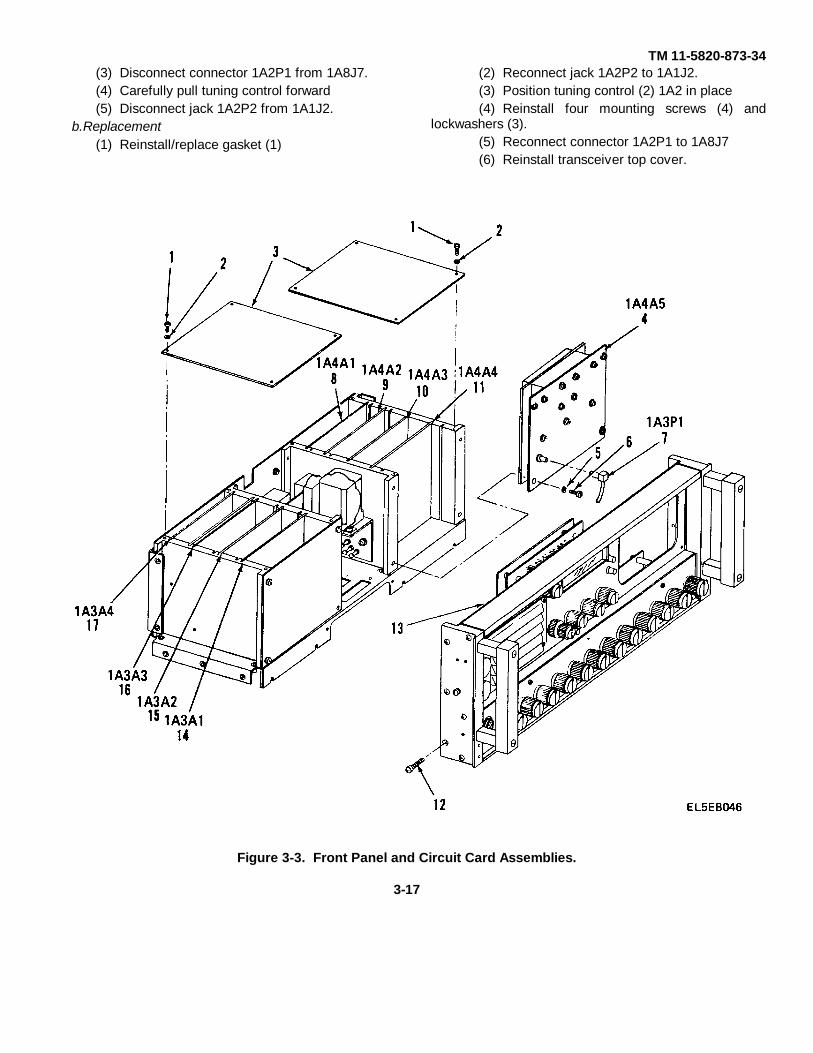
TM 11-5820-873-34(3) Disconnect connector 1A2P1 from 1A8J7.(4) Carefully pull tuning control forward(5) Disconnect jack 1A2P2 from 1A1J2.
b.Replacement(1) Reinstall/replace gasket (1)
(2) Reconnect jack 1A2P2 to 1A1J2.(3) Position tuning control (2) 1A2 in place(4) Reinstall four mounting screws (4) and
lockwashers (3).(5) Reconnect connector 1A2P1 to 1A8J7(6) Reinstall transceiver top cover.
Figure 3-3. Front Panel and Circuit Card Assemblies.
3-17
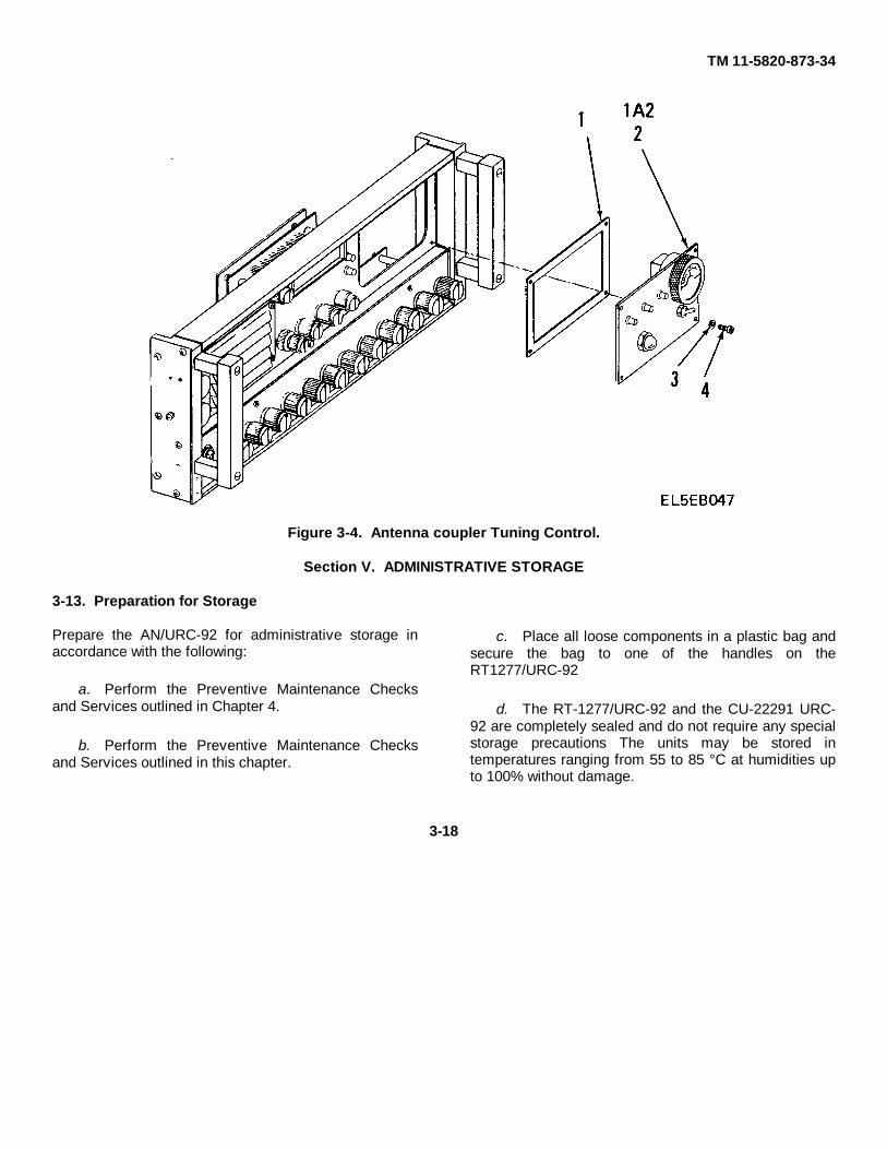
TM 11-5820-873-34
Figure 3-4. Antenna coupler Tuning Control.
Section V. ADMINISTRATIVE STORAGE
3-13. Preparation for Storage
Prepare the AN/URC-92 for administrative storage inaccordance with the following:
a. Perform the Preventive Maintenance Checksand Services outlined in Chapter 4.
b. Perform the Preventive Maintenance Checksand Services outlined in this chapter.
c. Place all loose components in a plastic bag andsecure the bag to one of the handles on theRT1277/URC-92
d. The RT-1277/URC-92 and the CU-22291 URC-92 are completely sealed and do not require any specialstorage precautions The units may be stored intemperatures ranging from 55 to 85 °C at humidities upto 100% without damage.
3-18
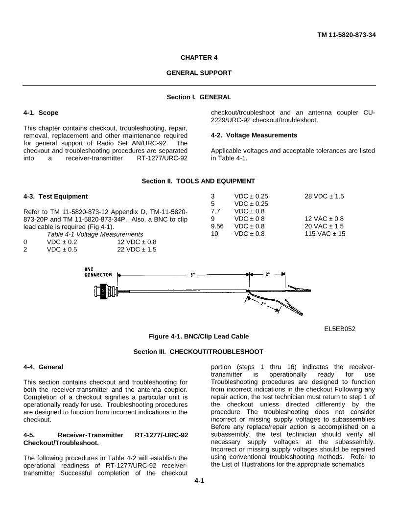
TM 11-5820-873-34
CHAPTER 4
GENERAL SUPPORT
Section I. GENERAL
4-1. Scope
This chapter contains checkout, troubleshooting, repair,removal, replacement and other maintenance requiredfor general support of Radio Set AN/URC-92. Thecheckout and troubleshooting procedures are separatedinto a receiver-transmitter RT-1277/URC-92
checkout/troubleshoot and an antenna coupler CU-2229/URC-92 checkout/troubleshoot.
4-2. Voltage Measurements
Applicable voltages and acceptable tolerances are listedin Table 4-1.
Section II. TOOLS AND EQUIPMENT
4-3. Test Equipment
Refer to TM 11-5820-873-12 Appendix D, TM-11-5820-873-20P and TM 11-5820-873-34P. Also, a BNC to cliplead cable is required (Fig 4-1).
Table 4-1 Voltage Measurements0 VDC ± 0.2 12 VDC ± 0.82 VDC ± 0.5 22 VDC ± 1.5
3 VDC ± 0.25 28 VDC ± 1.55 VDC ± 0.257.7 VDC ± 0.89 VDC ± 0 8 12 VAC ± 0 89.56 VDC ± 0.8 20 VAC ± 1.510 VDC ± 0.8 115 VAC ± 15
EL5EB052Figure 4-1. BNC/Clip Lead Cable
Section III. CHECKOUT/TROUBLESHOOT
4-4. General
This section contains checkout and troubleshooting forboth the receiver-transmitter and the antenna coupler.Completion of a checkout signifies a particular unit isoperationally ready for use. Troubleshooting proceduresare designed to function from incorrect indications in thecheckout.
4-5. Receiver-Transmitter RT-1277/-URC-92Checkout/Troubleshoot.
The following procedures in Table 4-2 will establish theoperational readiness of RT-1277/URC-92 receiver-transmitter Successful completion of the checkout
portion (steps 1 thru 16) indicates the receiver-transmitter is operationally ready for useTroubleshooting procedures are designed to functionfrom incorrect indications in the checkout Following anyrepair action, the test technician must return to step 1 ofthe checkout unless directed differently by theprocedure The troubleshooting does not considerincorrect or missing supply voltages to subassembliesBefore any replace/repair action is accomplished on asubassembly, the test technician should verify allnecessary supply voltages at the subassembly.Incorrect or missing supply voltages should be repairedusing conventional troubleshooting methods. Refer tothe List of Illustrations for the appropriate schematics
4-1
TM 11-5820-873-34
Table 4-2. Checkout/Troubleshoot the Receiver-Transmitter RT-1277/URC-92STEP ACTION INDICATION NEXT STEP1 Remove top and bottom covers. Connect 115 VAC power cable
to POWER connector 1A8J3. Connect 50 ohm dummy loadthrough a thruline wattmeter to ANT jack 1A8J1. Connect aknown good Antenna Coupler CU-2229/URC-92 toACCESSORY jack 1A8J4. Set XMIT GAIN control fullycounterclockwise Set VOLUME control clockwise, 1/4 turnPush VFO control in (off). Set DIM control fully clockwise.
Step 2a
2a Set mode switch to LSB. ANTENNA COUPLER CONTROL meter lamp Yes: step 2bluminates. No: step 17
2b Check pilot lamp and display. Pilot lamp and display illuminate. Yes: step 2cNo: step 29
2c Rotate DIM control one position counterclockwise. Then rotateDIM control another position counterclockwise.
Pilot lamp and display intensity dim, then go out.Meter lamp retains intensity, then goes out.
Yes: step 3a No: step 42
3a Set FREQ CONTROL switch to A. Set FREQUENCY Acontrols to 1.5000 MHz. Rotate 100 KHz control throughpositions 4, 3, 2, 1, and 0.
LOW FREQ LIMIT lamp illuminates and speaker noiselevel decreases.
Yes: step 3b No: step 44
3b Rotate 100 KHz control through positions 6, 7, 8, and 9. LOW FREQ LIMIT lamp is out and receiver transmitteris enabled.
Yes: step 3c No: step 44
3c Set FREQ CONTROL switch to B. Set FRE QUENCY Bcontrols to 1.5000 MHz. Rotate 100 KHz control thru positions4, 3, 2, 1, and 0.
LOW FREQ LIMIT lamp illluminates. Yes: step 3d No: step 50
3d Rotate 100 KHz control thru positions 6, 7, 8, and 9. LOW FREQ LIMIT lamp is out. Yes. step 3e No: step 503e Set FREQ CONTROL switch to A. Set FREQUENCY A
controls to 1.6000 MHz. Increase VOLUME control until noiseis heard in speaker.
Noise is heard in speaker. Yes: step 3f No: step 54
3f Connect known good headphone to 1A1J3. Noise is heard in headphone. Yes: step3g No: step 2803g Disconnect headphone. Connect known good handset. Noise is heard in ear piece of handset. Yes: step 3h No: step 2893h Disconnect handset. Rotate RF GAIN control counterclockwise
and observe meter.Front panel meter reading increases to almost fullscale deflection.
Yes: step 4a No: step 64
4a Return RF GAIN control to fully clockwise position andVOLUME control to 1/4 turn clockwise. Connect a known goodCW key at the KEY jack. Set FREQUENCY A controls to29.9950 MHz. Set mode switch to CW. Depress CW key.
Sidetone is heard in speaker. Yes: step 4b No: step 77
4b Depress CW key and observe wattmeter. Wattmeter indicates 100 W ± 10 W. Yes: step 5a No: step 745a Connect oscilloscope across dummy load. Set oscilloscope to
.2 V/division. Set FREQUENCY A controls to 29.9995 MHz.Set mode switch to LSB. Connect microphone to MICconnector. Key microphone and observe oscilloscope.
Oscilloscope displays waveform similar to Fig.
4-2A, less than 2 V peak-to-peak.
Yes: step 5b No: step 163
5b Set mode switch to USB. Key microphone and observeoscilloscope.
Oscilloscope displays waveform similar to Fig. 4-2A,less than 2 V peak-to-peak.
Yes: step 5c No: step 163
5c Set oscilloscope to 50 V/division. Key, and speak intomicrophone. Increase XMT GAIN control until no furtherincrease peak-to-peak voltage is observed.
Oscilloscope displays waveform similar to Fig. 4-2A,190 V peak-to-peak, maximum.
Yes: step 5d No: step 165
5d Set mode switch to LSB Key and speak into microphone.Increase XMT Gain until no further increase in peak-to-peak voltage is observed.
Oscilloscope displays waveform similar to Fig. 4-2A,190 V peak-to-peak.
Yes: step 5e No: step 175
5e Set mode switch to AM. Key and speak into microphone.Observe oscilloscope.
Oscilloscope displays waveform similar to Fig. 4-B,modulated carrier signal.
Yes: step 6a No: step 177
6a Connect frequency counter to oscilloscope vertical amplifieroutput. Connect oscilloscope across dummy load. SetFREQUENCY A controls to 1.6000 MHz. Turn XMT GAINControl fully counterclockwise. Key microphone. Starting with100 Hz control, rotate each FREQUENCY A control through itsentire range.
Frequency counter and front panel readouts agree foreach frequency.
Yes: step6b No: step 185
4-2

TM 11-5820-873-34
Table 4-2. Checkout/Troubleshoot the Receiver-Transmitter RT-1277/URC-92--ContinuedSTEP ACTION INDICATION NEXT STEP6b Set FREQ CONTROL switch to B. Repeat step 6a
using FREQUENCY B controls.Frequency counter and front panel readouts agree for eachfrequency.
Yes: step 6c No: step 211
6c Set FREQ CONTROL switch to A. Pull out VFOPULL control (VFO on).
VFO lamp illuminates. Yes: step 6d No: step 215
6d Connect frequency counter to oscilloscope verticalamplifier output. Connect oscilloscope across dummyload. Set FREQUENCY A controls to 2.000 MHz. Keymicrophone. Rotate VFO PULL control through itsentire range.
Frequency counter indicates 2.0000 MHz ± 5 KHzminimum.
Yes: step7a No: step 218
7a Set FREQ CONTROL to A XMT B RCV. Keymicrophone. Rotate FREQUENCY B, 10 KHz control.
Frequency counter indicates 1.6000 MHz and front panelreadouts agree.
Yes: step 7b No: step 223
7b Release microphone key. Observe front panel readoutand rotate FREQUENCY A, 10 KHz control.
No readout change occurs Yes: step 82 No: step 223
8a Disconnect antenna coupler control cable. DisconnectCW key and mic. Remove dummy load from ANT jack1A8J1. Connect signal generator to ANT jack 1A8J1.Connect Audio VTVM to PHONE jack 1A1J3. Setmode switch to LSB. Set FREQ CONTROL to B SetFREQUENCY B controls to 29.9994 MHz. AdjustVOLUME CONTROL for VTVM indication of -20 dB.Set signal generator output level to 0.5 uV. Adjustsignal generator frequency to approximately 29.9994MHz, until VTVM indication peaks.
Audio VTVM indicates -10 dB or more. Yes: step 8b No: step 225
8b Repeat step 8a substituting the followingFREQUENCY B, and signal generator frequencysettings.
Audio VTVM indicates -10 dB or more. Yes: step 9a No: step292
16.0100 MHz 10.0100MHz 7.5100 MHz5.0100 MHz3.5100 MHz2.0100 MHz1.6100 MHz
9a Set mode switch to USB Return FREQUENCY Bswitches to 29.9994 MHz. Adjust signal generatorfrequency to approximately 29.9994 MHz, until VTMindication peaks.
Audio VTVM indicates at least -10 dB or more. Yes: step 9b No: step 295
9b Set mode switch to AM, FREQUENCY B controls to29.9994 MHz. Signal generator output level to 3.0 uV,frequency to 29.9994 MHz, 30%, 1 KHz modulation.Adjust signal generator for peak VTVM indication.Adjust VOLUME control for -10 dB VTVM Indication.Remove modulation from signal generator output.
VTVM indicates less than -20 dB. Yes: step 9c No: step 242
9c Set mode switch to LSB. Set FREQUENCY Bswitches to 20.000 MHz. Disconnect VTVM fromPHONE jack. Increase VOLUME control until noise isheard. Rotate 1 MHz control thru each of its positions.
At each position, noise blanks momentarily then returns. Yes: step 10 No: step 297
10 Set mode switch to OFF. Disconnect control cable atreceiver-transmitter 1A8J4. Connect multimeterbetween ACCESSORY Connector 1A8J4-P andground. Set mode switch to AM. Slowly adjustANTENNA coupler CONTROL gain control 1A2R2thru its entire range.
Meter indicates a range between + 12 and +22 VDC ± 10% Yes: step 11 No: step 264
11 Reset gain control 1A2R2 to 14.5 VDC ± 0.5 VDC.Set mode switch to OFF. Disconnect dummy loadfrom antenna jack lA8Jl. Connect RF and controlcables between the receiver-transmitter and a knowngood CU-2229/URC-92 Antenna Coupler Connect a50 ohm dummy load to the Antenna Coupler antennapost and ground post using a BNC/clip lead cable.
Step 12
4-3
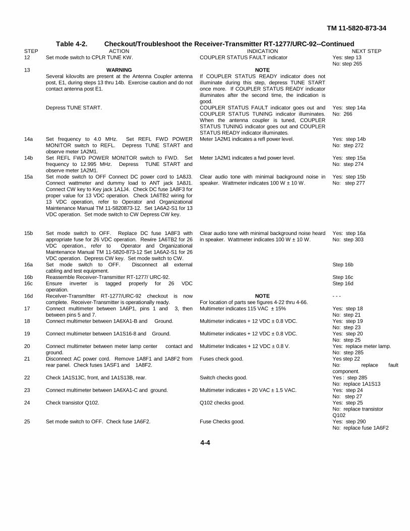
TM 11-5820-873-34
Table 4-2. Checkout/Troubleshoot the Receiver-Transmitter RT-1277/URC-92--ContinuedSTEP ACTION INDICATION NEXT STEP12 Set mode switch to CPLR TUNE KW. COUPLER STATUS FAULT indicator Yes: step 13
No: step 26513 WARNING NOTE
Several kilovolts are present at the Antenna Coupler antennapost, E1, during steps 13 thru 14b. Exercise caution and do notcontact antenna post E1.
If COUPLER STATUS READY indicator does notilluminate during this step, depress TUNE STARTonce more. If COUPLER STATUS READY indicatorilluminates after the second time, the indication isgood.
Depress TUNE START. COUPLER STATUS FAULT indicator goes out andCOUPLER STATUS TUNING indicator illuminates.When the antenna coupler is tuned, COUPLERSTATUS TUNING indicator goes out and COUPLERSTATUS READY indicator illuminates.
Yes: step 14aNo: 266
14a Set frequency to 4.0 MHz. Set REFL FWD POWERMONITOR switch to REFL. Depress TUNE START andobserve meter 1A2M1.
Meter 1A2M1 indicates a refl power level. Yes: step 14bNo: step 272
14b Set REFL FWD POWER MONITOR switch to FWD. Setfrequency to 12.995 MHz. Depress TUNE START andobserve meter 1A2M1.
Meter 1A2M1 indicates a fwd power level. Yes: step 15aNo: step 274
15a Set mode switch to OFF Connect DC power cord to 1A8J3.Connect wattmeter and dummy load to ANT jack 1A8J1.Connect CW key to Key jack 1A1J4. Check DC fuse 1A8F3 forproper value for 13 VDC operation. Check 1A6TB2 wiring for13 VDC operation, refer to Operator and OrganizationalMaintenance Manual TM 11-5820873-12. Set 1A6A2-S1 for 13VDC operation. Set mode switch to CW Depress CW key.
Clear audio tone with minimal background noise inspeaker. Wattmeter indicates 100 W ± 10 W.
Yes: step 15bNo: step 277
15b Set mode switch to OFF. Replace DC fuse 1A8F3 withappropriate fuse for 26 VDC operation. Rewire 1A6TB2 for 26VDC operation., refer to Operator and OrganizationalMaintenance Manual TM 11-5820-873-12 Set 1A6A2-S1 for 26VDC operation. Depress CW key. Set mode switch to CW.
Clear audio tone with minimal background noise heardin speaker. Wattmeter indicates 100 W ± 10 W.
Yes: step 16aNo: step 303
16a Set mode switch to OFF. Disconnect all externalcabling and test equipment.
Step 16b
16b Reassemble Receiver-Transmitter RT-1277/ URC-92. Step 16c16c Ensure inverter is tagged properly for 26 VDC
operation.Step 16d
16d Recelver-Transmltter RT-1277/URC-92 checkout is nowcomplete. Receiver-Transmitter is operationally ready.
NOTEFor location of parts see figures 4-22 thru 4-66.
- - -
17 Connect multimeter between 1A6P1, pins 1 and 3, thenbetween pins 5 and 7.
Multimeter indicates 115 VAC ± 15% Yes: step 18No: step 21
18 Connect multimeter between 1A6XA1-B and Ground. Multimeter indicates + 12 VDC ± 0.8 VDC. Yes: step 19No: step 23
19 Connect multimeter between 1A1S16-8 and Ground. Multimeter indicates + 12 VDC ± 0.8 VDC. Yes: step 20No: step 25
20 Connect multimeter between meter lamp center contact andground.
Multimeter Indicates + 12 VDC ± 0.8 V. Yes: replace meter lamp.No: step 285
21 Disconnect AC power cord. Remove 1A8F1 and 1A8F2 fromrear panel. Check fuses 1ASF1 and 1A8F2.
Fuses check good. Yes step 22No: replace faultycomponent.
22 Check 1A1S13C, front, and 1A1S13B, rear. Switch checks good. Yes : step 285No: replace 1A1S13
23 Connect multimeter between 1A6XA1-C and ground. Multimeter indicates + 20 VAC ± 1.5 VAC. Yes: step 24No: step 27
24 Check transistor Q102. Q102 checks good. Yes: step 25No: replace transistorQ102
25 Set mode switch to OFF. Check fuse 1A6F2. Fuse Checks good. Yes: step 290No: replace fuse 1A6F2
4-4
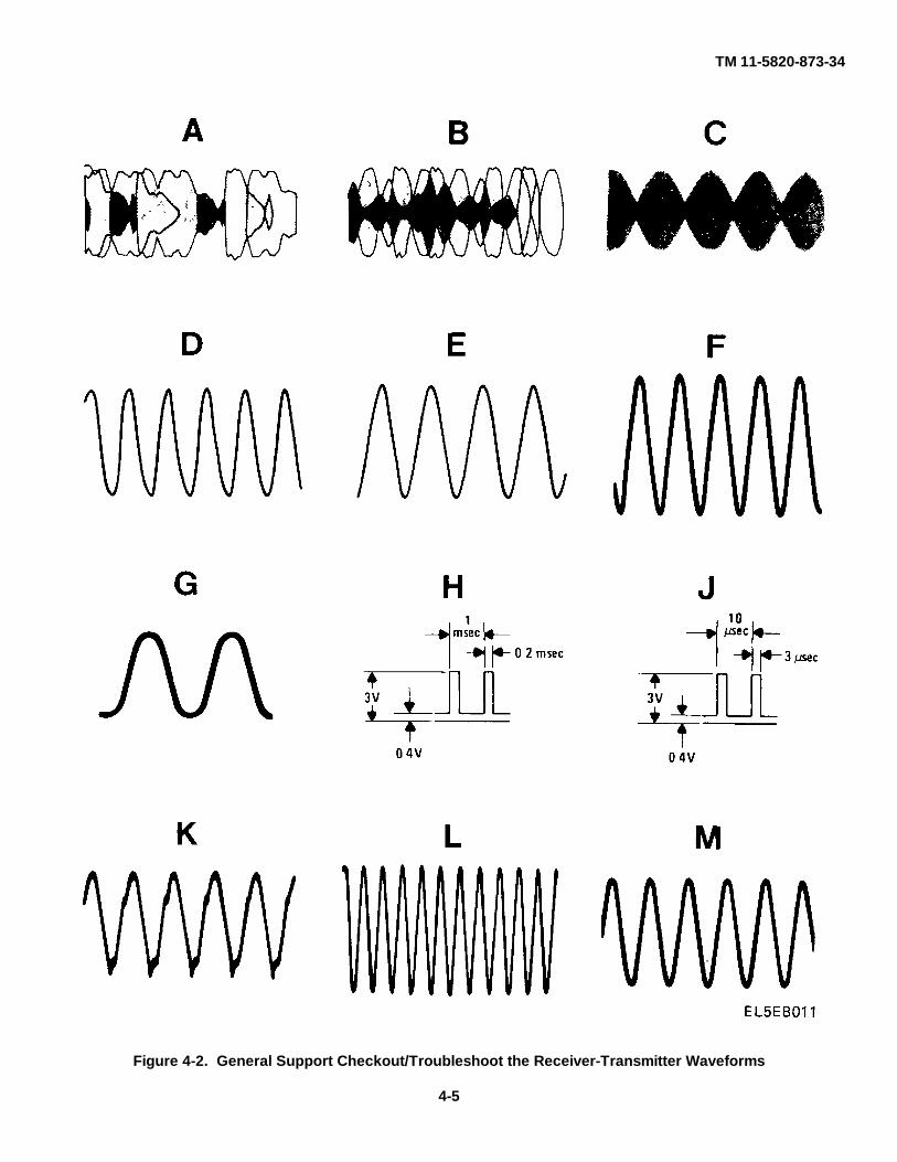
TM 11-5820-873-34
Figure 4-2. General Support Checkout/Troubleshoot the Receiver-Transmitter Waveforms
4-5
TM 11-5820-873-34
Table 4-2. Checkout/Troubleshoot the Receiver-Transmitter RT-1277/URC-92--ContinuedSTEP ACTION INDICATION NEXT STEP26 Connect multimeter between 1A1S16-7 and ground. Multimeter indicates + 12 VDC ± 0.8 VDC. Yes: replace 1A1S16
No: step 28527 Set mode switch to OFF. Remove 1A6A1 from 1A6XA1.
Check continuity between 1A6XA1 pins C and 3.Continuity checks good. Yes: step 28
No: replace transformer1A6T1.
28 Continuity check 1A6TB1 pins E1 to E3, and pins E5 to E6. Continuity checks good. Yes: step 285No: replace transformer
1A6T1.29 Connect multimeter between 1A6XA1-15 and ground. Multimeter indicates + 5 VDC ± 0.25 VDC. Yes: step 31
No: step 3230 Connect multimeter between 1A1S16-3 and ground. Multimeter indicates + 5 VDC ± 0.25 VDC. Yes: step 31
No: step 3631 Connect multimeter between 1A1DS3 center contact and
ground.Multimeter indicates + 5 VDC ± 0.25 VDC. Yes: replace 1A1DS3
No: step 28532 Connect multimeter between 1A6XA1-P and ground. Multimeter indicates + 12 VDC ± 0.8 VDC. Yes: step 33
No: step 35Yes: step 34
33 Check transistor 1A6Q103. Transistor 1A6Q103 checks good. No: replace transistor1A6Q103
34 Check fuse 1A6A1F3. Fuse checks good. Yes: step 286No: replace fuse 1A6A1F3
35 Set mode switch to OFF. Remove 1A6XA1 from 1A6A1.Continuity checks 1A6XA11 pin P to pin 13.
Continuity checks good. Yes: step 36No: replace transformer
1A6T136 Check components 1A1Q101, 1A1C5, and 1A1C7. Components check good. Yes: step 37
No: replace faulty com-ponent.
37 Connect multimeter between 1A1S16-3 and ground. Multimeter indicates + 5 VDC ± 0.25 VDC. Yes: step 39No: step 38
38 Connect multimeter between 1A6A1F3 and A6A1C9 junctionand ground.
Multimeter indicates + 10 to + 22 VDC. Yes: step 285No: step 286
39 Connect multimeter between 1A1A3P1-44 and ground. Multimeter indicates + 5 VDC ± 0.25 VDC. Yes: step 288No: step 40
40 Connect multimeter between 1A1A2-1 and ground. Multimeter indicates + 5 VDC ± 0.25 VDC. Yes: step 289No: step 41
41 Connect multimeter between 1A1S16-4 and ground. Multimeter indicates + 5 VDC ± 0.25 VDC. Yes: step 285No: replace switch
1A1S1642 Connect multimeter between 1A1S16-2 and ground. Multimeter indicates + 3 VDC ± 0.25 VDC. Yes: step 43
No: replace switch 1A1S1643 Check components 1A1CRF53. lA1CR54, and 1A1CR55. Components check good. Yes: step 285
No: replace faulty component.
44 Connect multimeter between 1A1DS1-1 center contact andground.
Multimeter indicates + 12 VDC ± 0.8 VDC. Yes: replace 1A1DS1No: step 45
45 Connect multimeter between 1A1S1A, rear, pin 4 and ground. Multimeter indicates + 12 VDC ± 0.8 VDC. Yes: step 46No: step 48
46 Connect multimeter between 1A1S2C, rear, pin 4 and ground. Multimeter indicates + 12 VDC ± 0.8 VDC. Yes: step 47No: step 49Yes: step 48
47 Check diode 1A1CR16. 1A1CR16 checks good. No: replace diode1A1CR16
Yes: step 49
48 Check switch 1A1S15. 1A1S15 checks good. No: replace switch1A1S15
Yes: step 52
49 Check switches 1A1SlA rear, 1A1S2C rear, and 1A 1S3B rear. Components check good. No: replace faultycomponent.
50 Set FREQ CONTROL switch to B. Set FREQUENCY Bcontrols to 1.5000 MHz. Rotate 100 KHz control thru positions4, 3, 2, 1 and 0.
LOW FREQ LIMIT lamp illuminates sometimes. Yes: step 52No: replace switch 1A1S9
51 Check the following components 1A1S7A rear, 1A1S8C rear,1A1S9B rear, 1A1S15 and 1A1CR37.
Component d check good. Yes: step 285No: replace faultycomponent.
4-6
TM 11-5820-873-34
Table 4-2. Checkout/Troubleshoot the Receiver-Transmitter RT-1277/URC-92--ContinuedSTEP52 Connect multimeter between 1A3A5-B and ground. Multimeter indicates + 12 VDC ± 0.8 VDC. Yes: step 53
No: step 28553 Connect multimeter between 1A1A5XA4-14 and ground. Multimeter indicates + 10 VDC ± 2 VDC. Yes: step 290
No: step 28754 Connect oscilloscope probe to 1A1A1-E3, ground lead to
ground.Check for noise above ambient level. Yes: step 55
No: step 5455 Connect oscilloscope to speaker 1A1LS1, signal input terminal,
ground lead to ground.Check for noise above ambient level. Yes: replace speaker
1A1LS1No: step 56
56 Check resistor 1A1R50. 1A1R50 checks good. Yes: step 57No: replace resistor
1A1R5057 Check 1A1J3. 1A1J3 checks good. Yes: step 285
No: replace 1A1J358 Connect oscilloscope probe to 1A3A5-M, ground lead to
ground.Check for noise above ambient level. Yes: step 59
No: step 6059 Connect oscilloscope probe to 1A1A1-E4 ground lead to
ground.Check for noise above ambient level. Yes: step 250
No: step 6160 Connect oscilloscope probe to 1A3XA4J4-18, ground lead to
ground.Check for noise above ambient level. Yes: step287
No: step 62Yes: step 285
61 Check resistor 1A1R51. 1A1R51 checks good. No: replace resistor1A1R51
62 Connect multimeter between 1A3XA4J4-12 and ground. Multimeter indicates + 12 VDC ± 0.8 VDC. Yes: step 290No: step 63
63 Connect multimeter between 1A3A5-E7 and ground. Multimeter indicates + 12 VDC ± 0.8 VDC. Yes: step 287No: step 63
64 Rotate RF GAIN control fully CCW. Connect multimeterbetween 1A3XA4J4-15 and ground.
Multimeter indicates + 12 VDC ± 0.8 VDC. Yes: step 65No: step 67
65 Connect multimeter between 1A3A5-E12 and ground. Multimeter indicates + 12 VDC ± 0.8 VDC. Yes: step 66No: step 287
66 Connect multimeter between 1A2M1 positive(+) pin and ground. Multimeter indicates + 12 VDC ± 0.8 VDC. Yes: replace meter 1A2M1No: step 69
67 Connect multimeter between 1A3A5-A and ground. Multimeter indicates + 12 VDC ± 0.8 VDC. Yes: step 68No: step 73
68 Connect multimeter between 1A3XA4J4-14 and ground. Multimeter indicates + 12 VDC ± 0.8 VDC. Yes: step 290No: step 287
69 Connect multimeter between 1A8P2 pins 12 and 13. Multimeter Indicates 0 V ± 2 VDC. Yes: step 70No: step 71
70 Check components 1A8K1 and 1A8CR1. Components check good. Yes: step 285No: replace faulty compo-
nent.71 Connect multimeter between 1A5XA4-11 and ground. Multimeter indicates + 12 VDC ± 2 VDC. Yes: step 292
No: step 7272 Remove Sideband Generator CCA 1A3A3. Multimeter indicates + 12 VDC ± 2 VDC. Yes: step 294
No: reinstall SidebandGenerator CCA1A3A3 and go tostep 285.
73 Check components 1A1R5, 1A1R54, and1A1CR50.
Components check good. Yes: step 285No: replace faulty compo-
nent.74 Connect oscilloscope probe to 1A3XA3J3-16, ground lead to
ground. Depress CW key.Oscilloscope displays waveform similar to Fig.4-2C.
Yes: step 75No: step 102
75 Remove 1A8P3 from 1A7J2. Connect wattmeter to 1A7J2center contact, ground lead to ground.Depress CW key.
Wattmeter indicates more than 90 watts. Yes: step 76No: step 79
76 Reconnect 1A7J2 to 1A8P3. Remove 1A8P5 from 1A5J4.Connect wattmeter to 1A5J4 center contact ground lead toground. Depress CW key.
Wattmeter indicates more than 90 watts. Yes: step 285No: step 82
77 Connect frequency counter to 1A3XA3J3-D,ground lead to ground. Depress CW key.
Frequency counter indicates 1 KHz. Yes: step 78No: step 290
78 Connect frequency counter to 1A3XA4J4-4, ground lead toground. Depress CW key.
Frequency counter indicates 1 KHz. Yes: step 290No: step 286
4-7
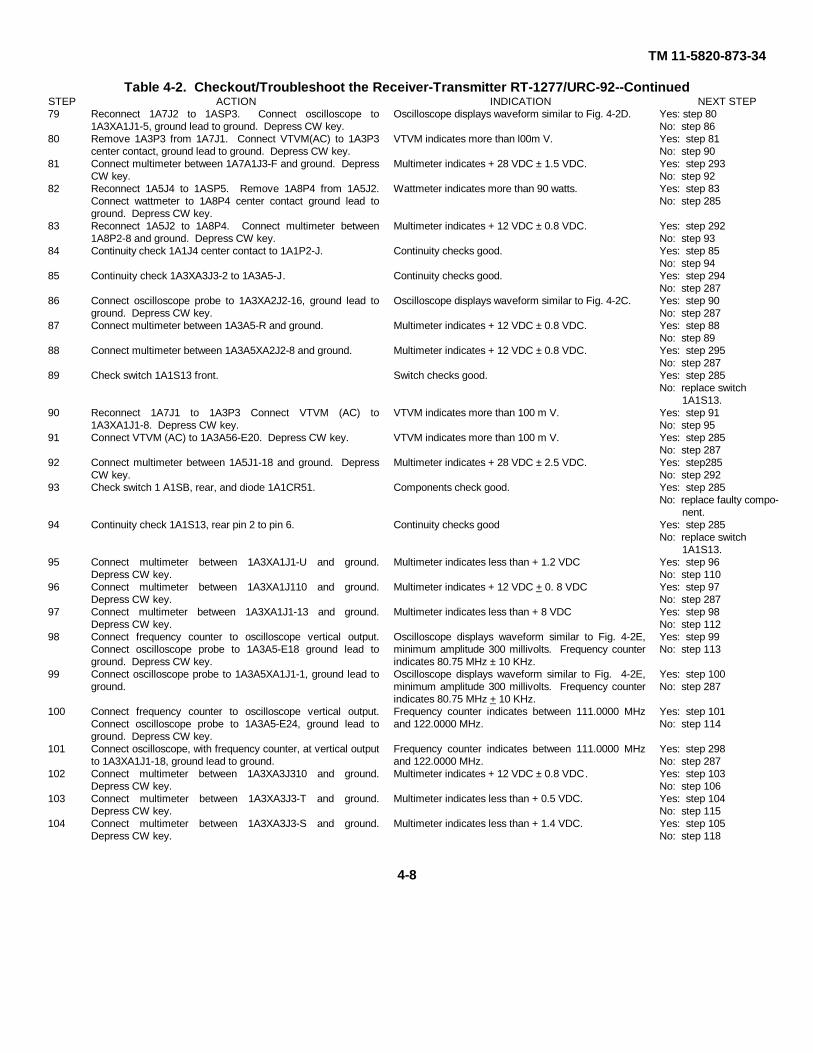
TM 11-5820-873-34
Table 4-2. Checkout/Troubleshoot the Receiver-Transmitter RT-1277/URC-92--ContinuedSTEP ACTION INDICATION NEXT STEP79 Reconnect 1A7J2 to 1ASP3. Connect oscilloscope to
1A3XA1J1-5, ground lead to ground. Depress CW key.Oscilloscope displays waveform similar to Fig. 4-2D. Yes: step 80
No: step 8680 Remove 1A3P3 from 1A7J1. Connect VTVM(AC) to 1A3P3
center contact, ground lead to ground. Depress CW key.VTVM indicates more than l00m V. Yes: step 81
No: step 9081 Connect multimeter between 1A7A1J3-F and ground. Depress
CW key.Multimeter indicates + 28 VDC ± 1.5 VDC. Yes: step 293
No: step 9282 Reconnect 1A5J4 to 1ASP5. Remove 1A8P4 from 1A5J2.
Connect wattmeter to 1A8P4 center contact ground lead toground. Depress CW key.
Wattmeter indicates more than 90 watts. Yes: step 83No: step 285
83 Reconnect 1A5J2 to 1A8P4. Connect multimeter between1A8P2-8 and ground. Depress CW key.
Multimeter indicates + 12 VDC ± 0.8 VDC. Yes: step 292No: step 93
84 Continuity check 1A1J4 center contact to 1A1P2-J. Continuity checks good. Yes: step 85No: step 94
85 Continuity check 1A3XA3J3-2 to 1A3A5-J. Continuity checks good. Yes: step 294No: step 287
86 Connect oscilloscope probe to 1A3XA2J2-16, ground lead toground. Depress CW key.
Oscilloscope displays waveform similar to Fig. 4-2C. Yes: step 90No: step 287
87 Connect multimeter between 1A3A5-R and ground. Multimeter indicates + 12 VDC ± 0.8 VDC. Yes: step 88No: step 89
88 Connect multimeter between 1A3A5XA2J2-8 and ground. Multimeter indicates + 12 VDC ± 0.8 VDC. Yes: step 295No: step 287
89 Check switch 1A1S13 front. Switch checks good. Yes: step 285No: replace switch
1A1S13.90 Reconnect 1A7J1 to 1A3P3 Connect VTVM (AC) to
1A3XA1J1-8. Depress CW key.VTVM indicates more than 100 m V. Yes: step 91
No: step 9591 Connect VTVM (AC) to 1A3A56-E20. Depress CW key. VTVM indicates more than 100 m V. Yes: step 285
No: step 28792 Connect multimeter between 1A5J1-18 and ground. Depress
CW key.Multimeter indicates + 28 VDC ± 2.5 VDC. Yes: step285
No: step 29293 Check switch 1 A1SB, rear, and diode 1A1CR51. Components check good. Yes: step 285
No: replace faulty compo-nent.
94 Continuity check 1A1S13, rear pin 2 to pin 6. Continuity checks good Yes: step 285No: replace switch
1A1S13.95 Connect multimeter between 1A3XA1J1-U and ground.
Depress CW key.Multimeter indicates less than + 1.2 VDC Yes: step 96
No: step 11096 Connect multimeter between 1A3XA1J110 and ground.
Depress CW key.Multimeter indicates + 12 VDC + 0. 8 VDC Yes: step 97
No: step 28797 Connect multimeter between 1A3XA1J1-13 and ground.
Depress CW key.Multimeter indicates less than + 8 VDC Yes: step 98
No: step 11298 Connect frequency counter to oscilloscope vertical output.
Connect oscilloscope probe to 1A3A5-E18 ground lead toground. Depress CW key.
Oscilloscope displays waveform similar to Fig. 4-2E,minimum amplitude 300 millivolts. Frequency counterindicates 80.75 MHz ± 10 KHz.
Yes: step 99No: step 113
99 Connect oscilloscope probe to 1A3A5XA1J1-1, ground lead toground.
Oscilloscope displays waveform similar to Fig. 4-2E,minimum amplitude 300 millivolts. Frequency counterindicates 80.75 MHz + 10 KHz.
Yes: step 100No: step 287
100 Connect frequency counter to oscilloscope vertical output.Connect oscilloscope probe to 1A3A5-E24, ground lead toground. Depress CW key.
Frequency counter indicates between 111.0000 MHzand 122.0000 MHz.
Yes: step 101No: step 114
101 Connect oscilloscope, with frequency counter, at vertical outputto 1A3XA1J1-18, ground lead to ground.
Frequency counter indicates between 111.0000 MHzand 122.0000 MHz.
Yes: step 298No: step 287
102 Connect multimeter between 1A3XA3J310 and ground.Depress CW key.
Multimeter indicates + 12 VDC ± 0.8 VDC. Yes: step 103No: step 106
103 Connect multimeter between 1A3XA3J3-T and ground.Depress CW key.
Multimeter indicates less than + 0.5 VDC. Yes: step 104No: step 115
104 Connect multimeter between 1A3XA3J3-S and ground.Depress CW key.
Multimeter indicates less than + 1.4 VDC. Yes: step 105No: step 118
4-8
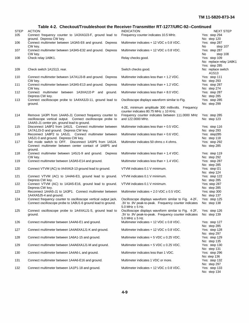
TM 11-5820-873-34
Table 4-2. Checkout/Troubleshoot the Receiver-Transmitter RT-1277/URC-92--ContinuedSTEP ACTION INDICATION NEXT STEP105 Connect frequency counter to 1A3XA3J3-F, ground lead to
ground. Depress CW key.Frequency counter indicates 10.5 MHz. Yes: step 294
No: step 120106 Connect multimeter between 1A3A5-E6 and ground. Depress
CW key.Multimeter indicates + 12 VDC ± 0.8 VDC. Yes: step 287
No step 107107 Connect multimeter between 1A3A5-E32 and ground. Depress
CW key.Multimeter indicates + 12 VDC ± 0.8 VDC. Yes: step 287
No step 108108 Check relay 1A8K1. Relay checks good. Yes: step 109
No: replace relay 1A8K1Yes: step 285
109 Check switch 1A1S13, rear. Switch checks good. No: replace switchA1S13
110 Connect multimeter between 1A7A1J3-B and ground. DepressCW key.
Multimeter indicates less than + 1.2 VDC. Yes: step 111No: step 293
111 Connect multimeter between 1A3A5-E13 and ground. DepressCW key.
Multimeter indicates less than + 1.2 VDC. Yes: step 287No: step 274
112 Connect multimeter between 1A3XA2J2-P and ground.Depress CW key.
Multimeter indicates less than + 8.0 VDC. Yes: step 287No: step 285
113 Connect oscilloscope probe to 1A4XA3J3-11, ground lead toground.
Oscilloscope displays waveform similar to Fig.
4-2E, minimum amplitude 300 millivolts. Frequencycounter indicates 80.75 MHz + 10 KHz.
Yes: step 285No: step 299
114 Remove 1A3Pl from 1A4A5-J1 Connect frequency counter tooscilloscope vertical output. Connect oscilloscope probe to1A4A5-J1 center pin, ground lead to ground.
Frequency counter indicates between 111.0000 MHzand 122.0000 MHz.
Yes: step 285No: step 123
115 Disconnect 1A8P2 from 1A5J1. Connect multimeter between1A7A1J3-D and ground. Depress CW key.
Multimeter indicates less than + 0.5 VDC. Yes: step 116No: step 293
116 Reconnect 1A8P2 to 1A5J1. Connect multimeter between1A5J1-0 and ground. Depress CW key.
Multimeter indicates less than + 0.6 VDC. Yes: step285No: step 118
117 Set mode switch to OFF. Disconnect 1A5P5 from 1A5J4.Connect multimeter between center contact of 1A8P5 andground.
Multimeter indicates 50 ohms ± 4 ohms. Yes: step 292No: step 285
118 Connect multimeter between 1A5J1-9 and ground. DepressCW key.
Multimeter indicates less than + 1.4 VDC. Yes: step 119No: step 292
119 Connect multimeter between 1A3A5-E14 and ground. Multimeter indicates less than + 1.4 VDC. Yes: step 287No: step 285
120 Connect VTVM (AC) to IA4XAlJl-13 ground lead to ground. VTVM indicates 0.1 V minimum. Yes: step l21No: step 124
121 Connect VTVM (AC) to 1A4A6-E3, ground lead to ground.Depress CW key.
VTVM indicates 0.1 V minimum. Yes: step 122No: step 285
122 Connect VTVM (AC) to 1A3A5-E16, ground lead to ground.Depress CW key.
VTVM indicates 0.1 V minimum. Yes: step 287No: step 285
123 Reconnect 1A4A5-J1 to 1A3P1. Connect multimeter between1A4XA5J5-4 and ground.
Multimeter indicates + 2.0 VDC ± 0.5 VDC. Yes: step 300No: step 137
124 Connect frequency counter to oscilloscope vertical output jack.Connect oscilloscope probe to 1A8U1-6 ground lead to ground.
Oscilloscope displays waveform similar to Fig. 4-2F,.3V to .9V peak-to-peak. Frequency counter indicates5.0 MHz ± 5 Hz.
Yes: step 125No: step 138
125 Connect oscilloscope probe to 1A4XA1J1-S, ground lead toground.
Oscilloscope displays waveform similar to Fig. 4-2F,.3V to .9V peak-to-peak. Frequency counter indicates5.0 MHz ± 5 Hz.
Yes: step 126No: step 139
126 Connect multimeter between 1A4A6-E1 and ground. Multimeter indicates + 12 VDC ± 0.8 VDC. Yes: step 127No: step 285
127 Connect multimeter between 1A4A6XA1J1-K and ground. Multimeter indicates + 12 VDC ± 0.8 VDC. Yes: step 128No: step 297
128 Connect multimeter between 1A6A1-15 and ground. Multimeter indicates + 5 VDC ± 0.25 VDC. Yes: step 129No: step 135
129 Connect multimeter between 1A4A6XA1J1-M and ground. Multimeter indicates + 5 VDC ± 0.25 VDC. Yes: step 130No: step 131
130 Connect multimeter between 1A4A6-L and ground. Multimeter indicates less than 1 VDC. Yes: step 296No: step 136
131 Connect multimeter between 1A4A6-E16 and ground. Multimeter indicates 1 VDC or more. Yes: step 132No: step 297
132 Connect multimeter between 1A1P1-18 and ground. Multimeter indicates + 12 VDC ± 0.8 VDC. Yes: step 133No: step 134
4-9
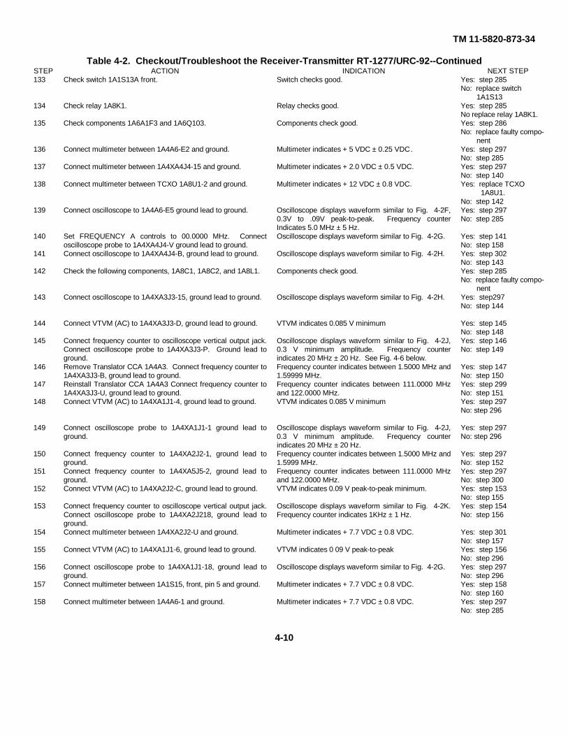
TM 11-5820-873-34
Table 4-2. Checkout/Troubleshoot the Receiver-Transmitter RT-1277/URC-92--ContinuedSTEP ACTION INDICATION NEXT STEP133 Check switch 1A1S13A front. Switch checks good. Yes: step 285
No: replace switch1A1S13
134 Check relay 1A8K1. Relay checks good. Yes: step 285No replace relay 1A8K1.
135 Check components 1A6A1F3 and 1A6Q103. Components check good. Yes: step 286No: replace faulty compo-
nent136 Connect multimeter between 1A4A6-E2 and ground. Multimeter indicates + 5 VDC ± 0.25 VDC. Yes: step 297
No: step 285137 Connect multimeter between 1A4XA4J4-15 and ground. Multimeter indicates + 2.0 VDC ± 0.5 VDC. Yes: step 297
No: step 140138 Connect multimeter between TCXO 1A8U1-2 and ground. Multimeter indicates + 12 VDC ± 0.8 VDC. Yes: replace TCXO
1A8U1.No: step 142
139 Connect oscilloscope to 1A4A6-E5 ground lead to ground. Oscilloscope displays waveform similar to Fig. 4-2F,0.3V to .09V peak-to-peak. Frequency counterIndicates 5.0 MHz ± 5 Hz.
Yes: step 297No: step 285
140 Set FREQUENCY A controls to 00.0000 MHz. Connectoscilloscope probe to 1A4XA4J4-V ground lead to ground.
Oscilloscope displays waveform similar to Fig. 4-2G. Yes: step 141No: step 158
141 Connect oscilloscope to 1A4XA4J4-B, ground lead to ground. Oscilloscope displays waveform similar to Fig. 4-2H. Yes: step 302No: step 143
142 Check the following components, 1A8C1, 1A8C2, and 1A8L1. Components check good. Yes: step 285No: replace faulty compo-
nent143 Connect oscilloscope to 1A4XA3J3-15, ground lead to ground. Oscilloscope displays waveform similar to Fig. 4-2H. Yes: step297
No: step 144
144 Connect VTVM (AC) to 1A4XA3J3-D, ground lead to ground. VTVM indicates 0.085 V minimum Yes: step 145No: step 148
145 Connect frequency counter to oscilloscope vertical output jack.Connect oscilloscope probe to 1A4XA3J3-P. Ground lead toground.
Oscilloscope displays waveform similar to Fig. 4-2J,0.3 V minimum amplitude. Frequency counterindicates 20 MHz ± 20 Hz. See Fig. 4-6 below.
Yes: step 146No: step 149
146 Remove Translator CCA 1A4A3. Connect frequency counter to1A4XA3J3-B, ground lead to ground.
Frequency counter indicates between 1.5000 MHz and1.59999 MHz.
Yes: step 147No: step 150
147 Reinstall Translator CCA 1A4A3 Connect frequency counter to1A4XA3J3-U, ground lead to ground.
Frequency counter indicates between 111.0000 MHzand 122.0000 MHz.
Yes: step 299No: step 151
148 Connect VTVM (AC) to 1A4XA1J1-4, ground lead to ground. VTVM indicates 0.085 V minimum Yes: step 297No: step 296
149 Connect oscilloscope probe to 1A4XA1J1-1 ground lead toground.
Oscilloscope displays waveform similar to Fig. 4-2J,0.3 V minimum amplitude. Frequency counterindicates 20 MHz ± 20 Hz.
Yes: step 297No: step 296
150 Connect frequency counter to 1A4XA2J2-1, ground lead toground.
Frequency counter indicates between 1.5000 MHz and1.5999 MHz.
Yes: step 297No: step 152
151 Connect frequency counter to 1A4XA5J5-2, ground lead toground.
Frequency counter indicates between 111.0000 MHzand 122.0000 MHz.
Yes: step 297No: step 300
152 Connect VTVM (AC) to 1A4XA2J2-C, ground lead to ground. VTVM indicates 0.09 V peak-to-peak minimum. Yes: step 153No: step 155
153 Connect frequency counter to oscilloscope vertical output jack.Connect oscilloscope probe to 1A4XA2J218, ground lead toground.
Oscilloscope displays waveform similar to Fig. 4-2K.Frequency counter indicates 1KHz ± 1 Hz.
Yes: step 154No: step 156
154 Connect multimeter between 1A4XA2J2-U and ground. Multimeter indicates + 7.7 VDC ± 0.8 VDC. Yes: step 301No: step 157
155 Connect VTVM (AC) to 1A4XA1J1-6, ground lead to ground. VTVM indicates 0 09 V peak-to-peak Yes: step 156No: step 296
156 Connect oscilloscope probe to 1A4XA1J1-18, ground lead toground.
Oscilloscope displays waveform similar to Fig. 4-2G. Yes: step 297No: step 296
157 Connect multimeter between 1A1S15, front, pin 5 and ground. Multimeter indicates + 7.7 VDC ± 0.8 VDC. Yes: step 158No: step 160
158 Connect multimeter between 1A4A6-1 and ground. Multimeter indicates + 7.7 VDC ± 0.8 VDC. Yes: step 297No: step 285
4-10
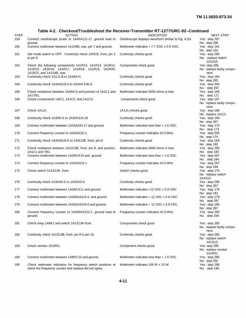
TM 11-5820-873-34
Table 4-2. Checkout/Troubleshoot the Receiver-Transmitter RT-1277/URC-92--ContinuedSTEP ACTION INDICATION NEXT STEP159 Connect oscilloscope probe to 1A4XA1J1-17, ground lead to
ground.Oscilloscope displays waveform similar to Fig. 4-2G. Yes: step 297
No: step 296160 Connect multimeter between 1A1S4B, rear, pin 7 and ground. Multimeter indicates + 7.7 VDC ± 0.8 VDC. Yes: step 161
No: step 162161 Set mode switch to OFF. Continuity check 1AlS15, front, pin 2
to pin 5.Continuity checks good. Yes: step 285
No: replace switch1A1S15
162 Check the following components 1A1R12, 1A1R13, 1A1R14,1A1R15, 1A1R16, 1A1R17, 1A1R18, 1A1R19, 1A1R20,1A1R22, and 1A1S4B, rear.
Components check good. Yes: step 285No: replace faulty compo-
nent.163 Continuity check 1A1J1-B to 1A3A5-H. Continuity checks good. Yes: step 164
No: step 285164 Continuity check 1A3XA3J3-3 to 1A3XA 5J5-H. Continuity checks good. Yes: step 294
No: step 297165 Check resistance between 1A3A5-D and junction of 1A1C1 and
1A1TB1.Multimeter indicates 5000 ohms or less Yes: step 166
No: step 171166 Check components 1AIC1, 1A1C2, and 1A1C3. Components check good. Yes: step 167
No: replace faulty compo-nent.
167 Check 1A1J1. 1A1J1 checks good. Yes: step 168No: replace 1A1J1
168 Continuity check 1A3A5-D to 1A3XA3J3-18 Continuity checks good. Yes: step 169No: step 287
169 Connect multimeter between 1A3XA3J3-17 and ground. Multimeter indicates less than + 1.6 VDC. Yes: step 170No: step 173
170 Connect frequency counter to 1A3XA2J2-1. Frequency counter indicates 10.5 MHz. Yes: step 295No: step 174
171 Continuity check 1A3XA5J5-D to 1AlS13B, front, pin 8. Continuity checks good. Yes: step 183No: step 182
172 Check resistance between 1A1S13B, front, pin 8, and junction,1A1C1 and TB1.
Multimeter indicates 5000 ohms or less Yes: step 285No: step 183
173 Connect multimeter between 1A3A5-E15 and ground. Multimeter indicates less than + 1.6 VDC. Yes: step 287No: step 184
174 Connect frequency counter to 1A3XA3J3-1. Frequency counter indicates 10.5 MHz. Yes: step 287No: step 294
175 Check switch 1A1S13A, front. Switch checks good. Yes: step 176No: replace switch1A1S13
176 Continuity check 1A3XA5-S to 1A3XA3-9. Continuity checks good. Yes: step 285No: step 287
177 Connect multimeter between 1A3A5-E11 and ground. Multimeter indicates +12 VDC ± 0 8 VDC Yes: step 178No: step 181
178 Connect multimeter between 1A3A5XA2J2-6 and ground. Multimeter indicates + 12 VDC ± 0 8 VDC Yes: step 179No: step 287
179 Connect multimeter between 1A3A5XA3J3-5 and ground. Multimeter indicates + 12 VDC ± 0 8 VDC Yes: step 180No: step 287
180 Connect frequency counter to 1A3A5XA2J2-1, ground lead toground.
Frequency counter indicates 10.5 MHz. Yes: step 295No: step 294
181 Check relay 1A8K1 and switch 1A1S13A front. Components check good. Yes: step 285No: replace faulty compo-
nent.182 Continuity check 1A1S13B, front, pin 8 to pin 10. Continuity checks good. Yes: step 285
No: replace switch1A1S13.
183 Check resistor 1A1R51. Component checks good. Yes: step 285No: replace resistor
1A1R51184 Connect multimeter between 1A8P2-10 and ground. Multimeter indicates less than + 1 6 VDC Yes: step 285
No: step 292185 Check wattmeter indication for frequency switch positions at
which the frequency counter and readout did not agree.Wattmeter indicates 100 W ± 10 W Yes: step 186
No: step 189
4-11
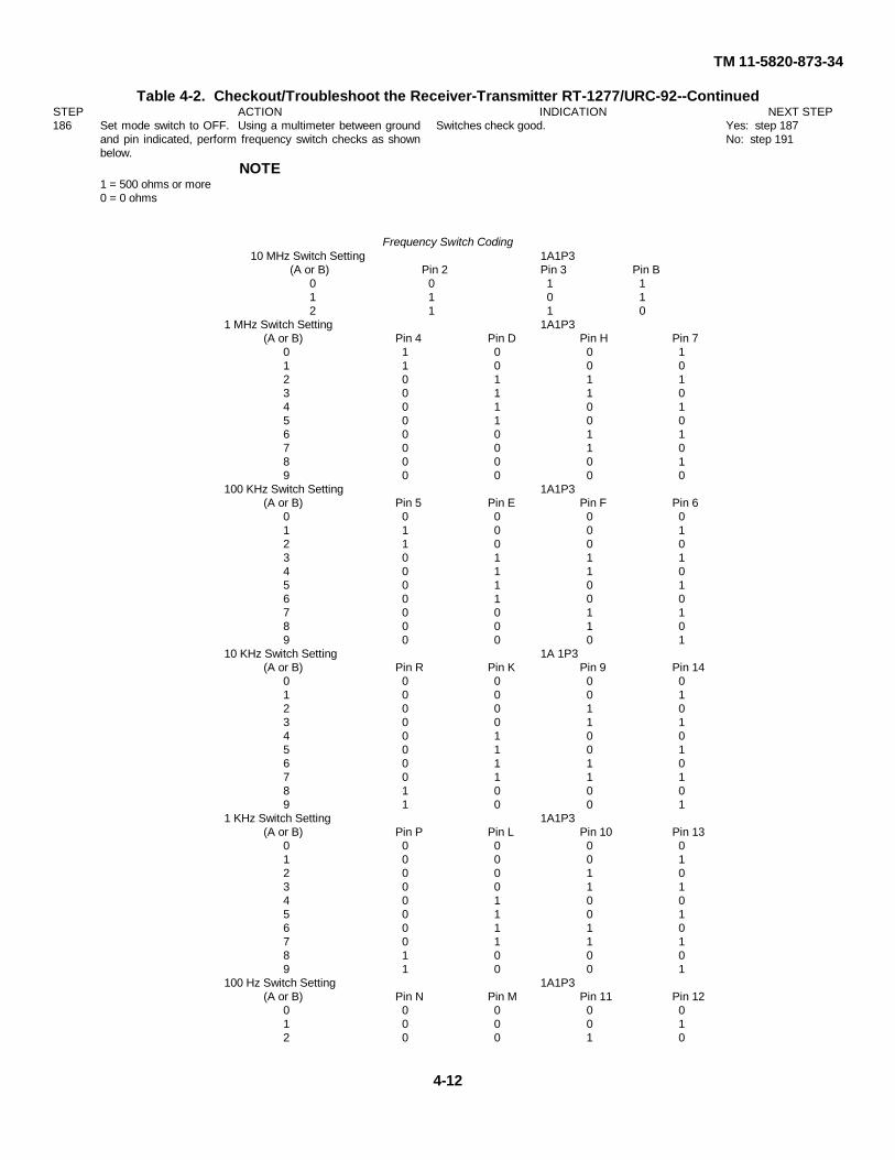
TM 11-5820-873-34
Table 4-2. Checkout/Troubleshoot the Receiver-Transmitter RT-1277/URC-92--ContinuedSTEP ACTION INDICATION NEXT STEP186 Set mode switch to OFF. Using a multimeter between ground
and pin indicated, perform frequency switch checks as shownbelow.
Switches check good. Yes: step 187No: step 191
NOTE1 = 500 ohms or more0 = 0 ohms
Frequency Switch Coding10 MHz Switch Setting 1A1P3
(A or B) Pin 2 Pin 3 Pin B0 0 1 11 1 0 12 1 1 0
1 MHz Switch Setting 1A1P3(A or B) Pin 4 Pin D Pin H Pin 7
0 1 0 0 11 1 0 0 02 0 1 1 13 0 1 1 04 0 1 0 15 0 1 0 06 0 0 1 17 0 0 1 08 0 0 0 19 0 0 0 0
100 KHz Switch Setting 1A1P3(A or B) Pin 5 Pin E Pin F Pin 6
0 0 0 0 01 1 0 0 12 1 0 0 03 0 1 1 14 0 1 1 05 0 1 0 16 0 1 0 07 0 0 1 18 0 0 1 09 0 0 0 1
10 KHz Switch Setting 1A 1P3(A or B) Pin R Pin K Pin 9 Pin 14
0 0 0 0 01 0 0 0 12 0 0 1 03 0 0 1 14 0 1 0 05 0 1 0 16 0 1 1 07 0 1 1 18 1 0 0 09 1 0 0 1
1 KHz Switch Setting 1A1P3(A or B) Pin P Pin L Pin 10 Pin 13
0 0 0 0 01 0 0 0 12 0 0 1 03 0 0 1 14 0 1 0 05 0 1 0 16 0 1 1 07 0 1 1 18 1 0 0 09 1 0 0 1
100 Hz Switch Setting 1A1P3(A or B) Pin N Pin M Pin 11 Pin 12
0 0 0 0 01 0 0 0 12 0 0 1 0
4-12
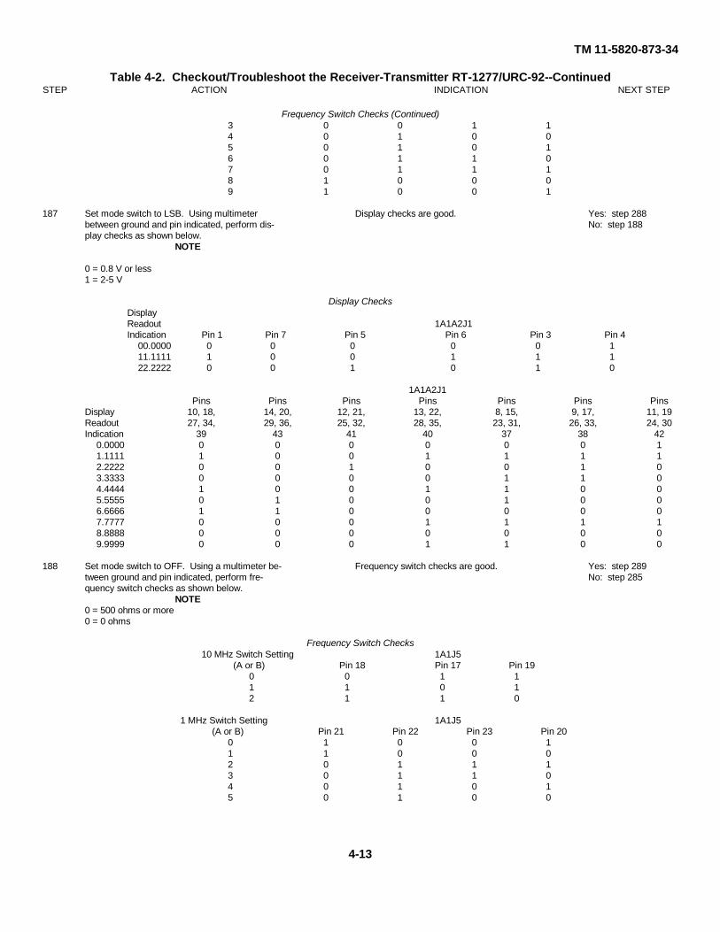
TM 11-5820-873-34
Table 4-2. Checkout/Troubleshoot the Receiver-Transmitter RT-1277/URC-92--ContinuedSTEP ACTION INDICATION NEXT STEP
Frequency Switch Checks (Continued)3 0 0 1 14 0 1 0 05 0 1 0 16 0 1 1 07 0 1 1 18 1 0 0 09 1 0 0 1
187 Set mode switch to LSB. Using multimeter Display checks are good. Yes: step 288between ground and pin indicated, perform dis- No: step 188play checks as shown below.
NOTE
0 = 0.8 V or less1 = 2-5 V
Display ChecksDisplayReadout 1A1A2J1Indication Pin 1 Pin 7 Pin 5 Pin 6 Pin 3 Pin 4
00.0000 0 0 0 0 0 111.1111 1 0 0 1 1 122.2222 0 0 1 0 1 0
1A1A2J1Pins Pins Pins Pins Pins Pins Pins
Display 10, 18, 14, 20, 12, 21, 13, 22, 8, 15, 9, 17, 11, 19Readout 27, 34, 29, 36, 25, 32, 28, 35, 23, 31, 26, 33, 24, 30Indication 39 43 41 40 37 38 42
0.0000 0 0 0 0 0 0 11.1111 1 0 0 1 1 1 12.2222 0 0 1 0 0 1 03.3333 0 0 0 0 1 1 04.4444 1 0 0 1 1 0 05.5555 0 1 0 0 1 0 06.6666 1 1 0 0 0 0 07.7777 0 0 0 1 1 1 18.8888 0 0 0 0 0 0 09.9999 0 0 0 1 1 0 0
188 Set mode switch to OFF. Using a multimeter be- Frequency switch checks are good. Yes: step 289tween ground and pin indicated, perform fre- No: step 285quency switch checks as shown below.
NOTE0 = 500 ohms or more0 = 0 ohms
Frequency Switch Checks10 MHz Switch Setting 1A1J5
(A or B) Pin 18 Pin 17 Pin 190 0 1 11 1 0 12 1 1 0
1 MHz Switch Setting 1A1J5(A or B) Pin 21 Pin 22 Pin 23 Pin 20
0 1 0 0 11 1 0 0 02 0 1 1 13 0 1 1 04 0 1 0 15 0 1 0 0
4-13
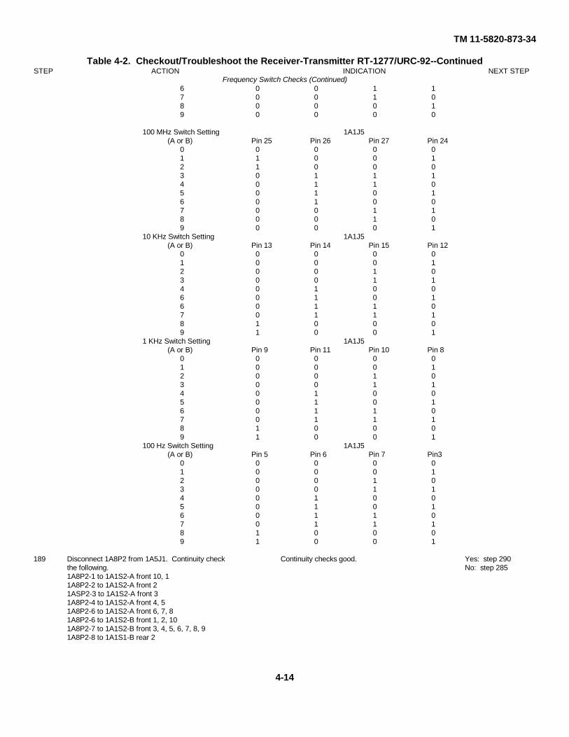
TM 11-5820-873-34
Table 4-2. Checkout/Troubleshoot the Receiver-Transmitter RT-1277/URC-92--ContinuedSTEP ACTION INDICATION NEXT STEP
Frequency Switch Checks (Continued)6 0 0 1 17 0 0 1 08 0 0 0 19 0 0 0 0
100 MHz Switch Setting 1A1J5(A or B) Pin 25 Pin 26 Pin 27 Pin 24
0 0 0 0 01 1 0 0 12 1 0 0 03 0 1 1 14 0 1 1 05 0 1 0 16 0 1 0 07 0 0 1 18 0 0 1 09 0 0 0 1
10 KHz Switch Setting 1A1J5(A or B) Pin 13 Pin 14 Pin 15 Pin 12
0 0 0 0 01 0 0 0 12 0 0 1 03 0 0 1 14 0 1 0 06 0 1 0 16 0 1 1 07 0 1 1 18 1 0 0 09 1 0 0 1
1 KHz Switch Setting 1A1J5(A or B) Pin 9 Pin 11 Pin 10 Pin 8
0 0 0 0 01 0 0 0 12 0 0 1 03 0 0 1 14 0 1 0 05 0 1 0 16 0 1 1 07 0 1 1 18 1 0 0 09 1 0 0 1
100 Hz Switch Setting 1A1J5(A or B) Pin 5 Pin 6 Pin 7 Pin3
0 0 0 0 01 0 0 0 12 0 0 1 03 0 0 1 14 0 1 0 05 0 1 0 16 0 1 1 07 0 1 1 18 1 0 0 09 1 0 0 1
189 Disconnect 1A8P2 from 1A5J1. Continuity check Continuity checks good. Yes: step 290the following. No: step 2851A8P2-1 to 1A1S2-A front 10, 11A8P2-2 to 1A1S2-A front 21ASP2-3 to 1A1S2-A front 31A8P2-4 to 1A1S2-A front 4, 51A8P2-6 to 1A1S2-A front 6, 7, 81A8P2-6 to 1A1S2-B front 1, 2, 101A8P2-7 to 1A1S2-B front 3, 4, 5, 6, 7, 8, 91A8P2-8 to 1A1S1-B rear 2
4-14
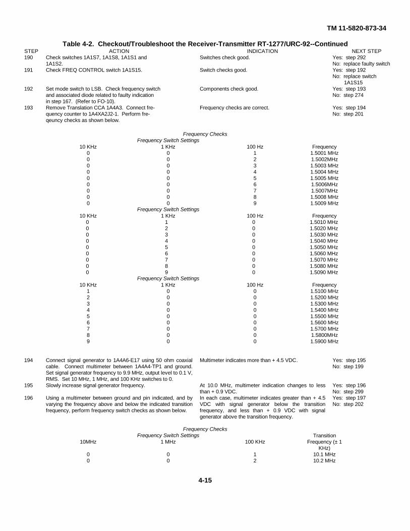
TM 11-5820-873-34
Table 4-2. Checkout/Troubleshoot the Receiver-Transmitter RT-1277/URC-92--ContinuedSTEP ACTION INDICATION NEXT STEP190 Check switches 1A1S7, 1A1S8, 1A1S1 and
1A1S2.Switches check good. Yes: step 292
No: replace faulty switch191 Check FREQ CONTROL switch 1A1S15. Switch checks good. Yes: step 192
No: replace switch1A1S15
192 Set mode switch to LSB. Check frequency switchand associated diode related to faulty indicationin step 167. (Refer to FO-10).
Components check good. Yes: step 193No: step 274
193 Remove Translation CCA 1A4A3. Connect fre-quency counter to 1A4XA2J2-1. Perform fre-qeuncy checks as shown below.
Frequency checks are correct. Yes: step 194No: step 201
Frequency ChecksFrequency Switch Settings
10 KHz 1 KHz 100 Hz Frequency0 0 1 1.5001 MHz0 0 2 1.5002MHz0 0 3 1.5003 MHz0 0 4 1.5004 MHz0 0 5 1.5005 MHz0 0 6 1.5006MHz0 0 7 1.5007MHz0 0 8 1.5008 MHz0 0 9 1.5009 MHz
Frequency Switch Settings10 KHz 1 KHz 100 Hz Frequency
0 1 0 1.5010 MHz0 2 0 1.5020 MHz0 3 0 1.5030 MHz0 4 0 1.5040 MHz0 5 0 1.5050 MHz0 6 0 1.5060 MHz0 7 0 1.5070 MHz0 8 0 1.5080 MHz0 9 0 1.5090 MHz
Frequency Switch Settings10 KHz 1 KHz 100 Hz Frequency
1 0 0 1.5100 MHz2 0 0 1.5200 MHz3 0 0 1.5300 MHz4 0 0 1.5400 MHz5 0 0 1.5500 MHz6 0 0 1.5600 MHz7 0 0 1.5700 MHz8 0 0 1.5800MHz9 0 0 1.5900 MHz
194 Connect signal generator to 1A4A6-E17 using 50 ohm coaxialcable. Connect multimeter between 1A4A4-TP1 and ground.Set signal generator frequency to 9.9 MHz, output level to 0.1 V,RMS. Set 10 MHz, 1 MHz, and 100 KHz switches to 0.
Multimeter indicates more than + 4.5 VDC. Yes: step 195No: step 199
195 Slowly increase signal generator frequency. At 10.0 MHz, multimeter indication changes to lessthan + 0.9 VDC.
Yes: step 196No: step 299
196 Using a multimeter between ground and pin indicated, and byvarying the frequency above and below the indicated transitionfrequency, perform frequency switch checks as shown below.
In each case, multimeter indicates greater than + 4.5VDC with signal generator below the transitionfrequency, and less than + 0.9 VDC with signalgenerator above the transition frequency.
Yes: step 197No: step 202
Frequency ChecksFrequency Switch Settings Transition
10MHz 1 MHz 100 KHz Frequency (± 1KHz)
0 0 1 10.1 MHz0 0 2 10.2 MHz
4-15
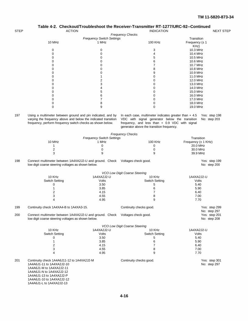
TM 11-5820-873-34
Table 4-2. Checkout/Troubleshoot the Receiver-Transmitter RT-1277/URC-92--ContinuedSTEP ACTION INDICATION NEXT STEP
Frequency ChecksFrequency Switch Settings Transition
10 MHz 1 MHz 100 KHz Frequency (± 1KHz)
0 0 3 10.3 MHz0 0 4 10.4 MHz0 0 5 10.5 MHz0 0 6 10.6 MHz0 0 7 10.7 MHz0 0 8 10.8 MHz0 0 9 10.9 MHz0 1 0 11.0 MHz0 2 0 12.0 MHz0 3 0 13.0 MHz0 4 0 14.0 MHz0 5 0 15.0 MHz0 6 0 16.0 MHz0 7 0 17.0 MHz0 8 0 18.0 MHz0 9 0 19.0 MHz
197 Using a multimeter between ground and pin indicated, and byvarying the frequency above and below the indicated transitionfrequency, perform frequency switch checks as shown below.
In each case, multimeter indicates greater than + 4.5VDC with signal generator below the transitionfrequency, and less than + 0.9 VDC with signalgenerator above the transition frequency.
Yes: step 198No: step 203
Frequency ChecksFrequency Switch Settings Transition
10 MHz 1 MHz 100 KHz Frequency (± 1 KHz)1 0 0 20.0 MHz2 0 0 30.0 MHz3 9 9 39.9 MHz
198 Connect multimeter between 1A4XA2J2-U and ground. Checklow digit coarse steering voltages as shown below.
Voltages check good. Yes: step 199No: step 200
VCO Low Digit Coarse Steering10 KHz 1A4XA2J2-U 10 KHz 1A4XA2J2-U
Switch Setting Volts Switch Setting Volts0 3.50 5 5.401 3.85 6 5.902 4.15 7 6.403 4.55 8 7.004 4.95 9 7.70
199 Continuity check 1A4XA4-B to 1A4XA3-15. Continuity checks good. Yes: step 299No: step 297
200 Connect multimeter between 1A4XA2J2-U and ground. Checklow digit coarse steering voltages as shown below.
Voltages check good. Yes: step 201No: step 208
VCO Low Digit Coarse Steering10 KHz 1A4XA2J2-U 10 KHz 1A4XA2J2-U
Switch Setting Volts Switch Setting Volts0 3.50 5 5.401 3.85 6 5.902 4.15 7 6.403 4.55 8 7.004 4.95 9 7.70
201 Continuity check 1A4A6J11-12 to 1A4XA2J2-M1A4A6J1-11 to 1A4XA2J2-101A4A6J1-M to 1A4XA2J2-111A4A6J1-N to 1A4XA2J2-121A4A6J1-13 to 1A4XA2J2-P1A4A6J1-10 to 1A4XA2J2-121A4A6J1-L to 1A4XA2J2-13
Continuity checks good. Yes: step 301No: step 297
4-16
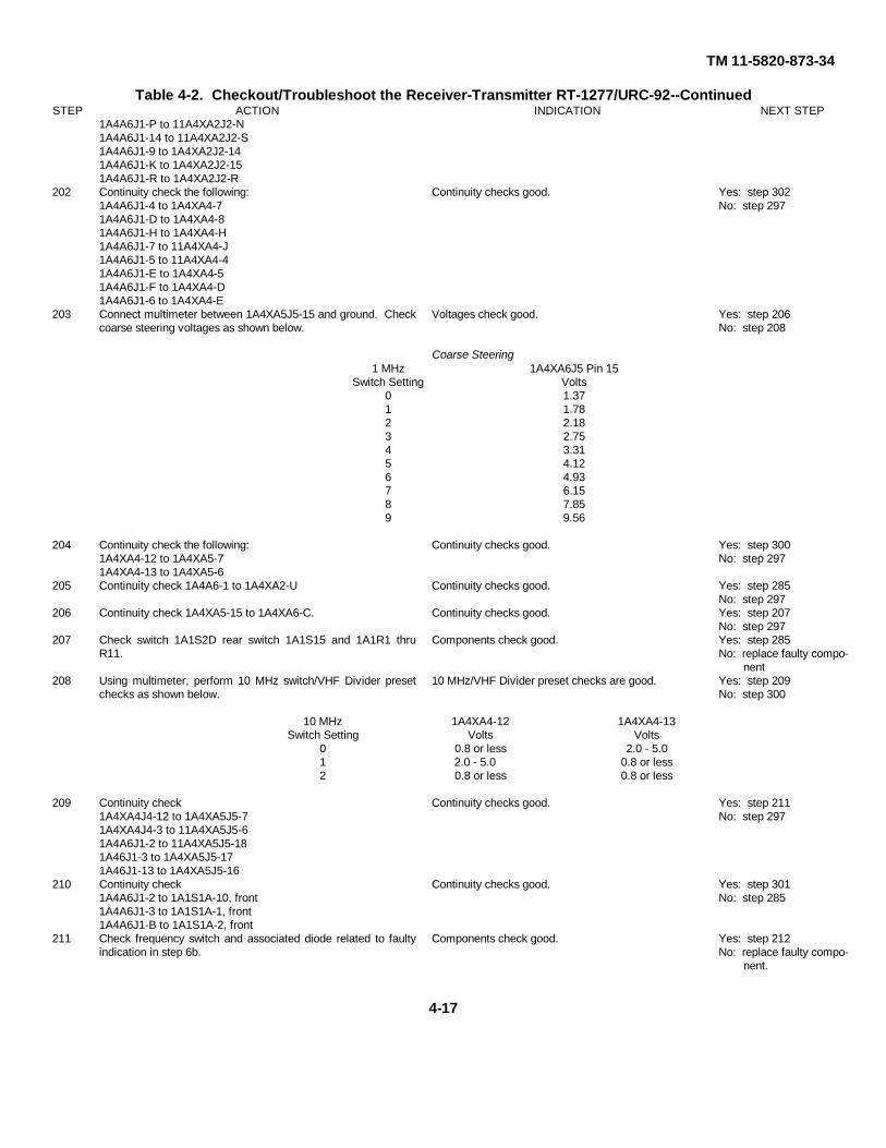
TM 11-5820-873-34
Table 4-2. Checkout/Troubleshoot the Receiver-Transmitter RT-1277/URC-92--ContinuedSTEP ACTION INDICATION NEXT STEP
1A4A6J1-P to 11A4XA2J2-N1A4A6J1-14 to 11A4XA2J2-S1A4A6J1-9 to 1A4XA2J2-141A4A6J1-K to 1A4XA2J2-151A4A6J1-R to 1A4XA2J2-R
202 Continuity check the following:1A4A6J1-4 to 1A4XA4-71A4A6J1-D to 1A4XA4-81A4A6J1-H to 1A4XA4-H1A4A6J1-7 to 11A4XA4-J1A4A6J1-5 to 11A4XA4-41A4A6J1-E to 1A4XA4-51A4A6J1-F to 1A4XA4-D1A4A6J1-6 to 1A4XA4-E
Continuity checks good. Yes: step 302No: step 297
203 Connect multimeter between 1A4XA5J5-15 and ground. Checkcoarse steering voltages as shown below.
Voltages check good. Yes: step 206No: step 208
Coarse Steering1 MHz 1A4XA6J5 Pin 15
Switch Setting Volts0 1.371 1.782 2.183 2.754 3.315 4.126 4.937 6.158 7.859 9.56
204 Continuity check the following:1A4XA4-12 to 1A4XA5-71A4XA4-13 to 1A4XA5-6
Continuity checks good. Yes: step 300No: step 297
205 Continuity check 1A4A6-1 to 1A4XA2-U Continuity checks good. Yes: step 285No: step 297
206 Continuity check 1A4XA5-15 to 1A4XA6-C. Continuity checks good. Yes: step 207No: step 297
207 Check switch 1A1S2D rear switch 1A1S15 and 1A1R1 thruR11.
Components check good. Yes: step 285No: replace faulty compo-
nent208 Using multimeter, perform 10 MHz switch/VHF Divider preset
checks as shown below.10 MHz/VHF Divider preset checks are good. Yes: step 209
No: step 300
10 MHz 1A4XA4-12 1A4XA4-13Switch Setting Volts Volts
0 0.8 or less 2.0 - 5.01 2.0 - 5.0 0.8 or less2 0.8 or less 0.8 or less
209 Continuity check1A4XA4J4-12 to 1A4XA5J5-71A4XA4J4-3 to 11A4XA5J5-61A4A6J1-2 to 11A4XA5J5-181A46J1-3 to 1A4XA5J5-171A46J1-13 to 1A4XA5J5-16
Continuity checks good. Yes: step 211No: step 297
210 Continuity check1A4A6J1-2 to 1A1S1A-10, front1A4A6J1-3 to 1A1S1A-1, front1A4A6J1-B to 1A1S1A-2, front
Continuity checks good. Yes: step 301No: step 285
211 Check frequency switch and associated diode related to faultyindication in step 6b.
Components check good. Yes: step 212No: replace faulty compo-
nent.
4-17
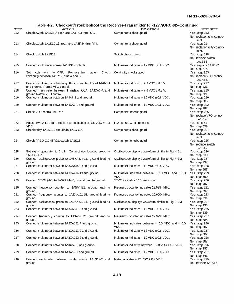
TM 11-5820-873-34
Table 4-2. Checkout/Troubleshoot the Receiver-Transmitter RT-1277/URC-92--ContinuedSTEP ACTION INDICATION NEXT STEP212 Check switch 1A1S8-D, rear, and 1A1R23 thru R33. Components check good. Yes: step 213
No: replace faulty compo-nent.
213 Check switch 1A1S10-13, rear, and 1A1R34 thru R44. Components check good. Yes: step 214No: replace faulty compo-
nent.214 Check switch 1A1S15. Switch checks good. Yes: step 285
No: replace switch1A1S15
215 Connect multimeter across 1A1DS2 contacts. Multimeter indicates + 12 VDC ± 0.8 VDC. Yes: replace 1A1DS2No: step 216
216 Set mode switch to OFF. Remove front panel. Checkcontinuity between 1A1R52, pins A and B.
Continuity checks good. Yes: step 285No: replace VFO control
1A1R52.217 Connect multimeter between synthesizer mother board 1A4A6-J
and ground. Rotate VFO control.Multimeter indicates + 7.6 VDC ± 0.8 V. Yes: step 217
No: step 221218 Connect multimeter between Translator CCA, 1A4XA3-A and
ground Rotate VFO control.Multimeter indicates + 7.6 VDC ± 0.8 V. Yes: step 219
No: step 221219 Connect multimeter between 1A4A6-8 and ground. Multimeter indicates + 12 VDC ± 0.8 VDC. Yes: step 220
No: step 285220 Connect multimeter between 1A4XA3-1 and ground. Multimeter indicates + 12 VDC ± 0.8 VDC. Yes: step 222
No: step 297221 Check VFO control 1A1R52. Component checks good. Yes: step 285
No: replace VFO control1A1R52.
222 Adjust 1A4A3-L22 for a multimeter indication of 7.6 VDC ± 0.8VDC.
L22 adjusts within tolerance. Yes: step 6dNo: step 299
223 Check relay 1A1K101 and diode 1A1CR17. Components check good. Yes: step 224No: replace faulty compo-
nent.224 Check FREQ CONTROL switch 1A1S15. Component checks good. Yes: step 285
No: replace switch1A1S15
225 Set signal generator to 0 dB. Connect oscilloscope probe to1A3XA2J2-5.
Oscilloscope displays waveform similar to Fig. 4-2L. Yes: step 226No: step 230
226 Connect oscilloscope probe to 1A3XA4J4-11, ground lead toground.
Oscilloscope displays waveform similar to Fig. 4-2M. Yes: step 227No: step 232
227 Connect multimeter between 1A3XA4J4-9 and ground. Multimeter indicates + 12 VDC ± 0.8 VDC. Yes: step 228No: step 287
228 Connect multimeter between 1A3XA4J4-13 and ground. Multimeter indicates between + 2.0 VDC and + 8.0VDC.
Yes: step 229No: step 290
229 Connect VTVM (AC) to 1A3XA4J4-6, ground lead to ground. VTVM indicates 0.1 V minimum. Yes: step 290No: step 187
230 Connect frequency counter to 1A5A4-E1, ground lead toground.
Frequency counter indicates 29.9994 MHz. Yes: step 231No: step 292
231 Connect frequency counter to 1A3XA1J1-15, ground lead toground.
Frequency counter indicates 29.9994 MHz. Yes: step 233No: step 234
232 Connect oscilloscope probe to 1A3XA2J2-11, ground lead toground.
Oscilloscope displays waveform similar to Fig. 4-2M. Yes: step 287No: step 236
233 Connect multimeter between 1A3XA1J1-3 and ground. Multimeter indicates + 12 VDC ± 0.8 VDC. Yes: step 235No: step 239
234 Connect frequency counter to 1A3A5-E22, ground lead toground.
Frequency counter indicates 29.9994 MHz. Yes: step 287No: step 285
235 Connect multimeter between 1A3XA1J1-P and ground. Multimeter indicates between + 2.0 VDC and + 8.0VDC.
Yes: step 298No: step 287
236 Connect multimeter between 1A3XA2J2-9 and ground. Multimeter indicates + 12 VDC ± 0.8 VDC. Yes: step 237No: step 287
237 Connect multimeter between 1A3XA2J2-3 and ground. Multimeter indicates + 12 VDC ± 0.8 VDC. Yes: step 238No: step 287
238 Connect multimeter between 1A3XA2-P and ground. Multimeter indicates between + 2.0 VDC + 0.8 VDC. Yes: step 295No: step 287
239 Connect multimeter between 1A3A5-E1 and ground. Multimeter indicates + 12 VDC ± 0.8 VDC. Yes: step 287No: step 241
240 Connect multimeter between mode switch, 1A1S13-2 andground.
Meter indicates + 12 VDC ± 0.8 VDC. Yes: step 285No: replace 1A1S13.
4-18
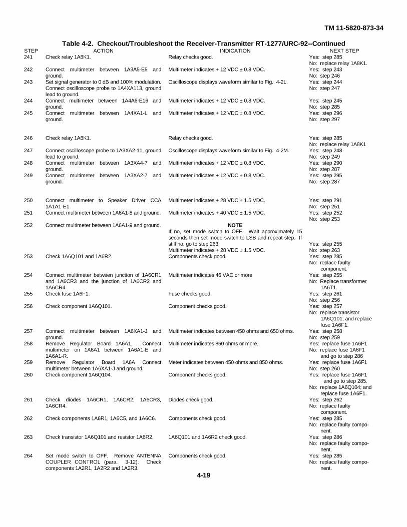
TM 11-5820-873-34
Table 4-2. Checkout/Troubleshoot the Receiver-Transmitter RT-1277/URC-92--ContinuedSTEP ACTION INDICATION NEXT STEP241 Check relay 1A8K1. Relay checks good. Yes: step 285
No: replace relay 1A8K1.242 Connect multimeter between 1A3A5-E5 and
ground.Multimeter indicates + 12 VDC ± 0.8 VDC. Yes: step 243
No: step 246243 Set signal generator to 0 dB and 100% modulation.
Connect oscilloscope probe to 1A4XA113, groundlead to ground.
Oscilloscope displays waveform similar to Fig. 4-2L. Yes: step 244No: step 247
244 Connect multimeter between 1A4A6-E16 andground.
Multimeter indicates + 12 VDC ± 0.8 VDC. Yes: step 245No: step 285
245 Connect multimeter between 1A4XA1-L andground.
Multimeter indicates + 12 VDC ± 0.8 VDC. Yes: step 296No: step 297
246 Check relay 1A8K1. Relay checks good. Yes: step 285No: replace relay 1A8K1
247 Connect oscilloscope probe to 1A3XA2-11, groundlead to ground.
Oscilloscope displays waveform similar to Fig. 4-2M. Yes: step 248No: step 249
248 Connect multimeter between 1A3XA4-7 andground.
Multimeter indicates + 12 VDC ± 0.8 VDC. Yes: step 290No: step 287
249 Connect multimeter between 1A3XA2-7 andground.
Multimeter indicates + 12 VDC ± 0.8 VDC. Yes: step 295No: step 287
250 Connect multimeter to Speaker Driver CCA1A1A1-E1.
Multimeter indicates + 28 VDC ± 1.5 VDC. Yes: step 291No: step 251
251 Connect multimeter between 1A6A1-8 and ground. Multimeter indicates + 40 VDC ± 1.5 VDC. Yes: step 252No: step 253
252 Connect multimeter between 1A6A1-9 and ground. NOTEIf no, set mode switch to OFF. Walt approximately 15seconds then set mode switch to LSB and repeat step. Ifstill no, go to step 263.Multimeter indicates + 28 VDC ± 1.5 VDC.
Yes: step 255No: step 263
253 Check 1A6Q101 and 1A6R2. Components check good. Yes: step 285No: replace faulty
component.254 Connect multimeter between junction of 1A6CR1
and 1A6CR3 and the junction of 1A6CR2 and1A6CR4.
Multimeter indicates 46 VAC or more Yes: step 255No: Replace transformer
1A6T1.255 Check fuse 1A6F1. Fuse checks good. Yes: step 261
No: step 256256 Check component 1A6Q101. Component checks good. Yes: step 257
No: replace transistor1A6Q101; and replacefuse 1A6F1.
257 Connect multimeter between 1A6XA1-J andground.
Multimeter indicates between 450 ohms and 650 ohms. Yes: step 258No: step 259
258 Remove Regulator Board 1A6A1. Connectmultimeter on 1A6A1 between 1A6A1-E and1A6A1-R.
Multimeter indicates 850 ohms or more. Yes: replace fuse 1A6F1No: replace fuse 1A6F1
and go to step 286259 Remove Regulator Board 1A6A Connect
multimeter between 1A6XA1-J and ground.Meter indicates between 450 ohms and 850 ohms. Yes: replace fuse 1A6F1
No: step 260260 Check component 1A6Q104. Component checks good. Yes: replace fuse 1A6F1
and go to step 285.No: replace 1A6Q104; and
replace fuse 1A6F1.261 Check diodes 1A6CR1, 1A6CR2, 1A6CR3,
1A6CR4.Diodes check good. Yes: step 262
No: replace faultycomponent.
262 Check components 1A6R1, 1A6C5, and 1A6C6. Components check good. Yes: step 285No: replace faulty compo-
nent.263 Check transistor 1A6Q101 and resistor 1A6R2. 1A6Q101 and 1A6R2 check good. Yes: step 286
No: replace faulty compo- nent.
264 Set mode switch to OFF. Remove ANTENNACOUPLER CONTROL (para. 3-12). Checkcomponents 1A2R1, 1A2R2 and 1A2R3.
Components check good. Yes: step 285No: replace faulty compo-
nent.4-19
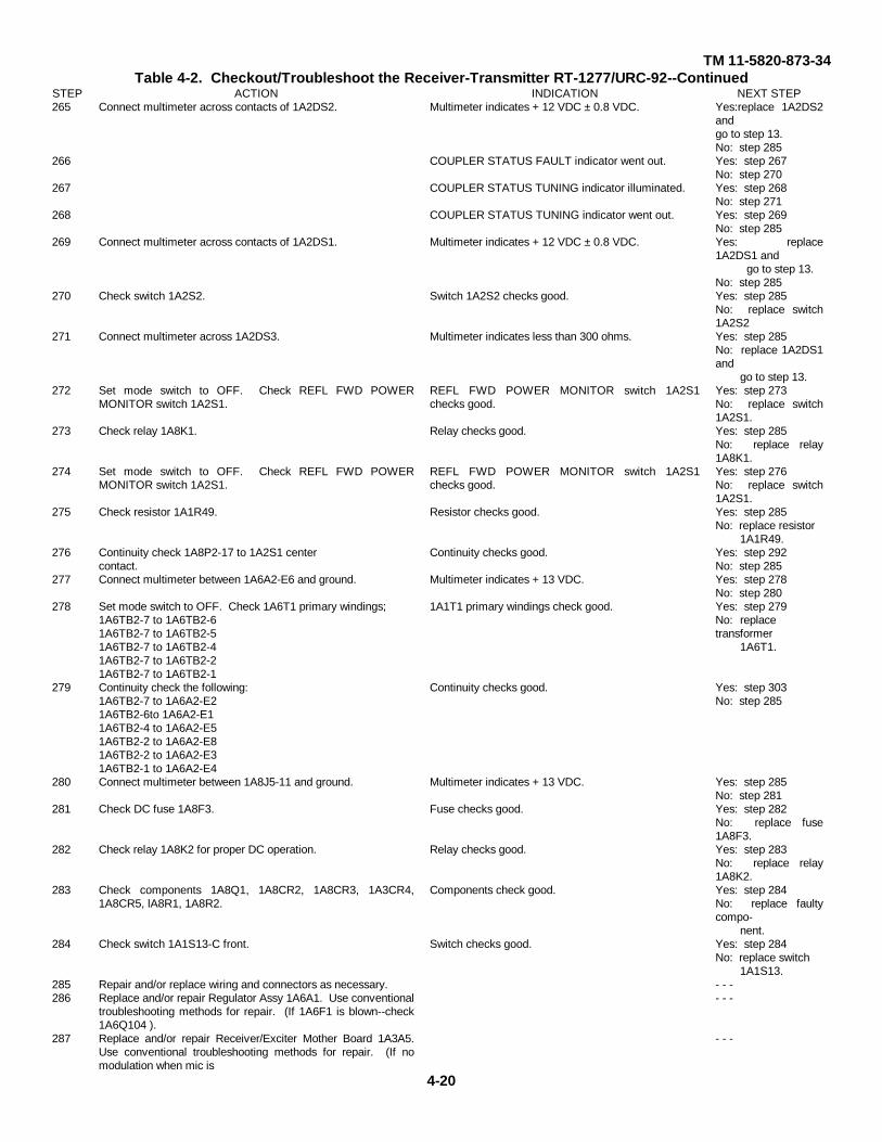
TM 11-5820-873-34Table 4-2. Checkout/Troubleshoot the Receiver-Transmitter RT-1277/URC-92--Continued
STEP ACTION INDICATION NEXT STEP265 Connect multimeter across contacts of 1A2DS2. Multimeter indicates + 12 VDC ± 0.8 VDC. Yes:replace 1A2DS2
andgo to step 13.No: step 285
266 COUPLER STATUS FAULT indicator went out. Yes: step 267No: step 270
267 COUPLER STATUS TUNING indicator illuminated. Yes: step 268No: step 271
268 COUPLER STATUS TUNING indicator went out. Yes: step 269No: step 285
269 Connect multimeter across contacts of 1A2DS1. Multimeter indicates + 12 VDC ± 0.8 VDC. Yes: replace1A2DS1 and
go to step 13.No: step 285
270 Check switch 1A2S2. Switch 1A2S2 checks good. Yes: step 285No: replace switch1A2S2
271 Connect multimeter across 1A2DS3. Multimeter indicates less than 300 ohms. Yes: step 285No: replace 1A2DS1and
go to step 13.272 Set mode switch to OFF. Check REFL FWD POWER
MONITOR switch 1A2S1.REFL FWD POWER MONITOR switch 1A2S1checks good.
Yes: step 273No: replace switch1A2S1.
273 Check relay 1A8K1. Relay checks good. Yes: step 285No: replace relay1A8K1.
274 Set mode switch to OFF. Check REFL FWD POWERMONITOR switch 1A2S1.
REFL FWD POWER MONITOR switch 1A2S1checks good.
Yes: step 276No: replace switch1A2S1.
275 Check resistor 1A1R49. Resistor checks good. Yes: step 285No: replace resistor
1A1R49.276 Continuity check 1A8P2-17 to 1A2S1 center
contact.Continuity checks good. Yes: step 292
No: step 285277 Connect multimeter between 1A6A2-E6 and ground. Multimeter indicates + 13 VDC. Yes: step 278
No: step 280278 Set mode switch to OFF. Check 1A6T1 primary windings;
1A6TB2-7 to 1A6TB2-61A6TB2-7 to 1A6TB2-51A6TB2-7 to 1A6TB2-41A6TB2-7 to 1A6TB2-21A6TB2-7 to 1A6TB2-1
1A1T1 primary windings check good. Yes: step 279No: replacetransformer
1A6T1.
279 Continuity check the following:1A6TB2-7 to 1A6A2-E21A6TB2-6to 1A6A2-E11A6TB2-4 to 1A6A2-E51A6TB2-2 to 1A6A2-E81A6TB2-2 to 1A6A2-E31A6TB2-1 to 1A6A2-E4
Continuity checks good. Yes: step 303No: step 285
280 Connect multimeter between 1A8J5-11 and ground. Multimeter indicates + 13 VDC. Yes: step 285No: step 281
281 Check DC fuse 1A8F3. Fuse checks good. Yes: step 282No: replace fuse1A8F3.
282 Check relay 1A8K2 for proper DC operation. Relay checks good. Yes: step 283No: replace relay1A8K2.
283 Check components 1A8Q1, 1A8CR2, 1A8CR3, 1A3CR4,1A8CR5, lA8R1, 1A8R2.
Components check good. Yes: step 284No: replace faultycompo-
nent.284 Check switch 1A1S13-C front. Switch checks good. Yes: step 284
No: replace switch1A1S13.
285 Repair and/or replace wiring and connectors as necessary. - - -286 Replace and/or repair Regulator Assy 1A6A1. Use conventional
troubleshooting methods for repair. (If 1A6F1 is blown--check1A6Q104 ).
- - -
287 Replace and/or repair Receiver/Exciter Mother Board 1A3A5.Use conventional troubleshooting methods for repair. (If nomodulation when mic is
- - -
4-20
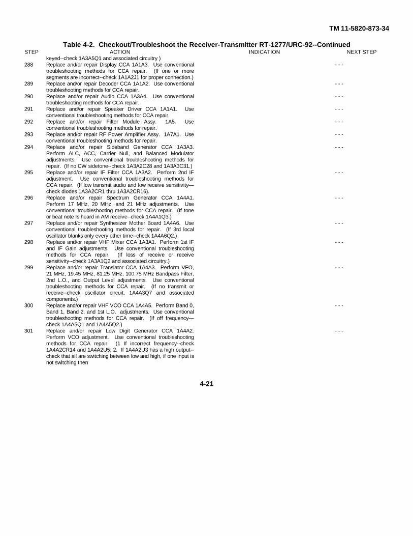
TM 11-5820-873-34
Table 4-2. Checkout/Troubleshoot the Receiver-Transmitter RT-1277/URC-92--ContinuedSTEP ACTION INDICATION NEXT STEP
keyed--check 1A3A5Q1 and associated circuitry )288 Replace and/or repair Display CCA 1A1A3. Use conventional
troubleshooting methods for CCA repair. (If one or moresegments are incorrect--check 1A1A2J1 for proper connection.)
- - -
289 Replace and/or repair Decoder CCA 1A1A2. Use conventionaltroubleshooting methods for CCA repair.
- - -
290 Replace and/or repair Audio CCA 1A3A4. Use conventionaltroubleshooting methods for CCA repair.
- - -
291 Replace and/or repair Speaker Driver CCA 1A1A1. Useconventional troubleshooting methods for CCA repair.
- - -
292 Replace and/or repair Filter Module Assy. 1A5. Useconventional troubleshooting methods for repair.
- - -
293 Replace and/or repair RF Power Amplifier Assy. 1A7A1. Useconventional troubleshooting methods for repair.
- - -
294 Replace and/or repair Sideband Generator CCA 1A3A3.Perform ALC, ACC, Carrier Null, and Balanced Modulatoradjustments. Use conventional troubleshooting methods forrepair. (If no CW sidetone--check 1A3A2C28 and 1A3A3C31.)
- - -
295 Replace and/or repair IF Filter CCA 1A3A2. Perform 2nd IFadjustment. Use conventional troubleshooting methods forCCA repair. (If low transmit audio and low receive sensitivity—check diodes 1A3A2CR1 thru 1A3A2CR16).
- - -
296 Replace and/or repair Spectrum Generator CCA 1A4A1.Perform 17 MHz, 20 MHz, and 21 MHz adjustments. Useconventional troubleshooting methods for CCA repair. (If toneor beat note Is heard in AM receive--check 1A4A1Q3.)
- - -
297 Replace and/or repair Synthesizer Mother Board 1A4A6. Useconventional troubleshooting methods for repair. (If 3rd localoscillator blanks only every other time--check 1A4A6Q2.)
- - -
298 Replace and/or repair VHF Mixer CCA 1A3A1. Perform 1st IFand IF Gain adjustments. Use conventional troubleshootingmethods for CCA repair. (If loss of receive or receivesensitivity--check 1A3A1Q2 and associated circuitry.)
- - -
299 Replace and/or repair Translator CCA 1A4A3. Perform VFO,21 MHz, 19.45 MHz, 81.25 MHz, 100.75 MHz Bandpass Filter,2nd L.O., and Output Level adjustments. Use conventionaltroubleshooting methods for CCA repair. (If no transmit orreceive--check oscillator circuit, 1A4A3Q7 and associatedcomponents.)
- - -
300 Replace and/or repair VHF VCO CCA 1A4A5. Perform Band 0,Band 1, Band 2, and 1st L.O. adjustments. Use conventionaltroubleshooting methods for CCA repair. (If off frequency—check 1A4A5Q1 and 1A4A5Q2.)
- - -
301 Replace and/or repair Low Digit Generator CCA 1A4A2.Perform VCO adjustment. Use conventional troubleshootingmethods for CCA repair. (1 If incorrect frequency--check1A4A2CR14 and 1A4A2U5; 2. If 1A4A2U3 has a high output--check that all are switching between low and high, if one input isnot switching then
- - -
4-21
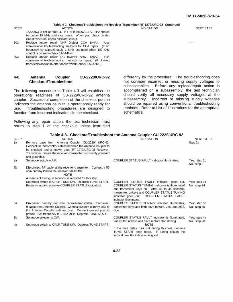
TM 11-5820-873-34
Table 4-2. Checkout/Troubleshoot the Receiver-Transmitter RT-1277/URC-92--ContinuedSTEP ACTION INDICATION NEXT STEP
1A4A2U3 is not at fault; 3. If TP3 is below 1.5 V, TP2 shouldbe below 15 MHz and vice versa. When yes, check dividercircuit; when on, check oscillator circuit.
302 Replace and/or repair VHF Divider CCA 1A4A4. Useconventional troubleshooting methods for CCA repair. (If offfrequency by approximately 1 MHz but good when 100 KHzcontrol is on zero--check 1A4A4U4.)
- - -
303 Replace and/or repair DC Inverter Assy. 1A6A2. Useconventional troubleshooting methods for repair. (If blowingtransistors and/or inverter doesn't work--check 1A6A2K1.)
4-6. Antenna Coupler CU-2229/URC-92Checkout/Troubleshoot
The following procedure in Table 4-3 will establish theoperational readiness of CU-2229/URC-92 antennacoupler. Successful completion of the checkout portionindicates the antenna coupler is operationally ready foruse. Troubleshooting procedures are designed tofunction from incorrect indications in the checkout.
Following any repair action, the test technician mustreturn to step 1 of the checkout unless instructed
differently by the procedure. The troubleshooting doesnot consider incorrect or missing supply voltages tosubassemblies. Before any replace/repair action isaccomplished on a subassembly, the test technicianshould verify all necessary supply voltages at thesubassembly. Incorrect or missing supply voltagesshould be repaired using conventional troubleshootingmethods. Refer to List of Illustrations for the appropriateschematics.
Table 4-3. Checkout/Troubleshoot the Antenna Coupler CU-2229/URC-92STEP ACTION INDICATION NEXT STEP1a Remove case from Antenna Coupler CU-2229/ URC-92.
Connect RF and control cables between the Antenna Coupler tobe checked and a known good RT-1277/URC-92 Receiver-Transmitter. Insure the receiver-transmitter is correctly poweredand grounded.
Step 2a
2a Set mode switch to AM. COUPLER STATUS FAULT indicator illuminates. Yes: step 2bNo: step 8
2b Disconnect RF cable at the receiver-transmitter. Connect a 50ohm dummy load to the receiver transmitter.
NOTEA means of timing, in seconds, is required for this step.Set mode switch to CPLR TUNE KW. Depress TUNE START.Begin timing and observe COUPLER STATUS indicators.
COUPLER STATUS FAULT indicator goes out.COUPLER STATUS TUNING indicator is illuminatedand transmitter keys on. After 35 to 45 seconds,transmitter unkeys and COUPLER STATUS TUNINGindicator goes out. COUPLER STATUS FAULTindicator illuminates.
Yes: step 3aNo: step 24
3a Disconnect dummy load from receiver-transmitter. Reconnectrf cable from Antenna Coupler. Connect 50 ohm dummy load tothe Antenna Coupler antenna post. Connect ground post toground. Set frequency to 1.602 MHz. Depress TUNE START.
COUPLET STATUS TUNING indicator illuminates,transmitter keys and both drive motors, 2M1 and 2M2,dive.
Yes: step 3bNo: step 50
3b Set mode selector to CW. COUPLER STATUS FAULT indicator is illuminated,transmitter unkeys and drive motors stop driving.
Yes: step 4aNo: step 90
4a Set mode switch to CPLR TUNE KW. Depress TUNE START. NOTEIf the time delay runs out during this test, depressTUNE START once more. If tuning occurs thesecond time the indication is good.
4-22
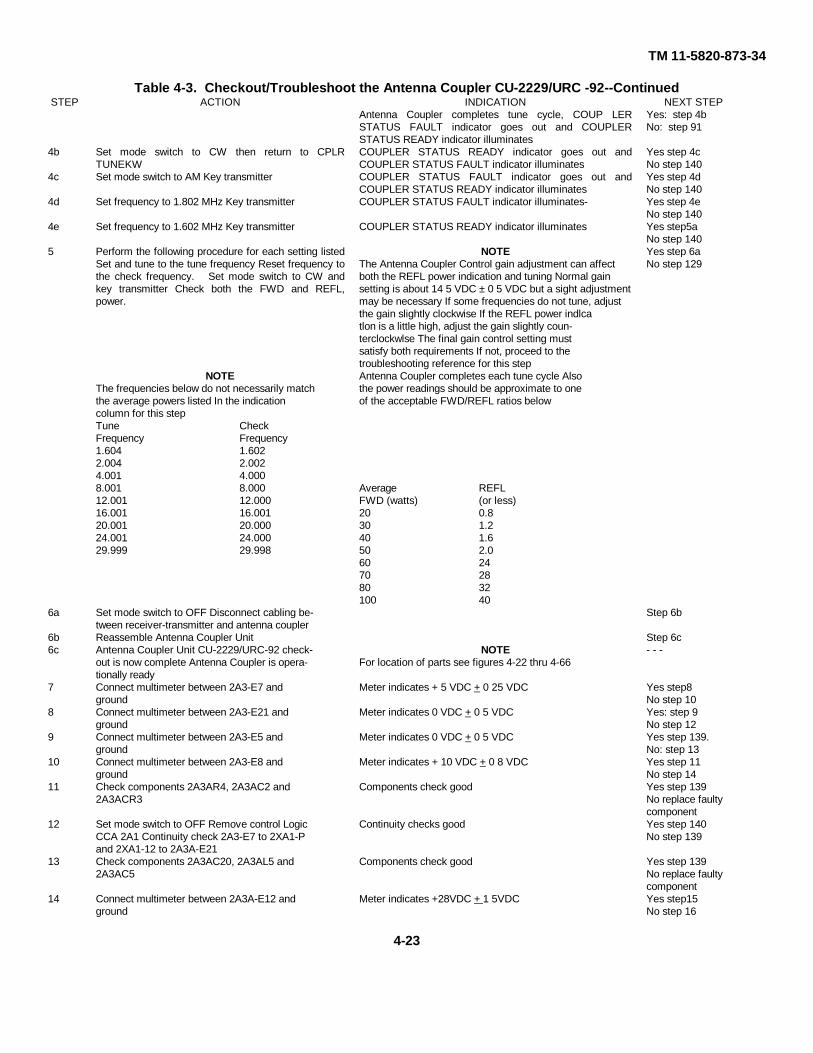
TM 11-5820-873-34
Table 4-3. Checkout/Troubleshoot the Antenna Coupler CU-2229/URC -92--ContinuedSTEP ACTION INDICATION NEXT STEP
Antenna Coupler completes tune cycle, COUP LERSTATUS FAULT indicator goes out and COUPLERSTATUS READY indicator illuminates
Yes: step 4bNo: step 91
4b Set mode switch to CW then return to CPLRTUNEKW
COUPLER STATUS READY indicator goes out andCOUPLER STATUS FAULT indicator illuminates
Yes step 4cNo step 140
4c Set mode switch to AM Key transmitter COUPLER STATUS FAULT indicator goes out andCOUPLER STATUS READY indicator illuminates
Yes step 4dNo step 140
4d Set frequency to 1.802 MHz Key transmitter COUPLER STATUS FAULT indicator illuminates- Yes step 4eNo step 140
4e Set frequency to 1.602 MHz Key transmitter COUPLER STATUS READY indicator illuminates Yes step5aNo step 140
5 Perform the following procedure for each setting listedSet and tune to the tune frequency Reset frequency tothe check frequency. Set mode switch to CW andkey transmitter Check both the FWD and REFL,power.
NOTEThe Antenna Coupler Control gain adjustment can affectboth the REFL power indication and tuning Normal gainsetting is about 14 5 VDC ± 0 5 VDC but a sight adjustmentmay be necessary If some frequencies do not tune, adjustthe gain slightly clockwise If the REFL power indlca
Yes step 6aNo step 129
tlon is a little high, adjust the gain slightly coun-terclockwlse The final gain control setting mustsatisfy both requirements If not, proceed to thetroubleshooting reference for this step
NOTE Antenna Coupler completes each tune cycle AlsoThe frequencies below do not necessarily match the power readings should be approximate to onethe average powers listed In the indication of the acceptable FWD/REFL ratios belowcolumn for this stepTune CheckFrequency Frequency1.604 1.6022.004 2.0024.001 4.0008.001 8.000 Average REFL12.001 12.000 FWD (watts) (or less)16.001 16.001 20 0.820.001 20.000 30 1.224.001 24.000 40 1.629.999 29.998 50 2.0
60 2470 2880 32100 40
6a Set mode switch to OFF Disconnect cabling be- Step 6btween receiver-transmitter and antenna coupler
6b Reassemble Antenna Coupler Unit Step 6c6c Antenna Coupler Unit CU-2229/URC-92 check- NOTE - - -
out is now complete Antenna Coupler is opera- For location of parts see figures 4-22 thru 4-66tionally ready
7 Connect multimeter between 2A3-E7 and Meter indicates + 5 VDC + 0 25 VDC Yes step8ground No step 10
8 Connect multimeter between 2A3-E21 and Meter indicates 0 VDC + 0 5 VDC Yes: step 9ground No step 12
9 Connect multimeter between 2A3-E5 and Meter indicates 0 VDC + 0 5 VDC Yes step 139.ground No: step 13
10 Connect multimeter between 2A3-E8 and Meter indicates + 10 VDC + 0 8 VDC Yes step 11ground No step 14
11 Check components 2A3AR4, 2A3AC2 and Components check good Yes step 1392A3ACR3 No replace faulty
component12 Set mode switch to OFF Remove control Logic Continuity checks good Yes step 140
CCA 2A1 Continuity check 2A3-E7 to 2XA1-P No step 139and 2XA1-12 to 2A3A-E21
13 Check components 2A3AC20, 2A3AL5 and Components check good Yes step 1392A3AC5 No replace faulty
component14 Connect multimeter between 2A3A-E12 and Meter indicates +28VDC + 1 5VDC Yes step15
ground No step 16
4-23
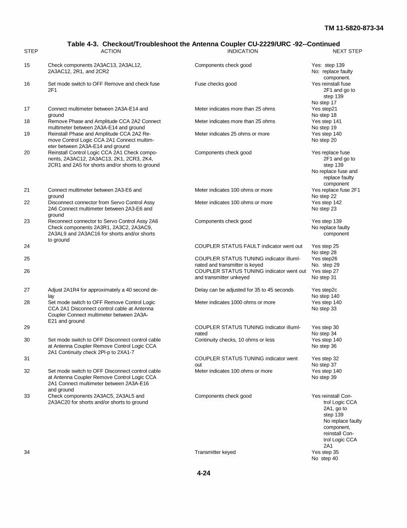
TM 11-5820-873-34
Table 4-3. Checkout/Troubleshoot the Antenna Coupler CU-2229/URC -92--ContinuedSTEP ACTION INDICATION NEXT STEP
15 Check components 2A3AC13, 2A3AL12, Components check good Yes: step 1392A3AC12, 2R1, and 2CR2 No: replace faulty
component.16 Set mode switch to OFF Remove and check fuse Fuse checks good Yes reinstall fuse
2F1 2F1 and go tostep 139
No step 1717 Connect multimeter between 2A3A-E14 and Meter indicates more than 25 ohms Yes step21
ground No step 1818 Remove Phase and Amplitude CCA 2A2 Connect Meter indicates more than 25 ohms Yes step 141
multimeter between 2A3A-E14 and ground No step 1919 Reinstall Phase and Amplitude CCA 2A2 Re- Meter indicates 25 ohms or more Yes step 140
move Control Logic CCA 2A1 Connect multim- No step 20eter between 2A3A-E14 and ground
20 Reinstall Control Logic CCA 2A1 Check compo- Components check good Yes replace fusenents, 2A3AC12, 2A3AC13, 2K1, 2CR3, 2K4, 2F1 and go to2CR1 and 2A5 for shorts and/or shorts to ground step 139
No replace fuse andreplace faultycomponent
21 Connect multimeter between 2A3-E6 and Meter indicates 100 ohms or more Yes replace fuse 2F1ground No step 22
22 Disconnect connector from Servo Control Assy Meter indicates 100 ohms or more Yes step 1422A6 Connect multimeter between 2A3-E6 and No step 23ground
23 Reconnect connector to Servo Control Assy 2A6 Components check good Yes step 139Check components 2A3R1, 2A3C2, 2A3AC9, No replace faulty2A3AL9 and 2A3AC16 for shorts and/or shorts componentto ground
24 COUPLER STATUS FAULT indicator went out Yes step 25No step 28
25 COUPLER STATUS TUNING indicator illuml- Yes step26nated and transmitter is keyed No. step 29
26 COUPLER STATUS TUNING indicator went out Yes step 27and transmitter unkeyed No step 31
27 Adjust 2A1R4 for approximately a 40 second de- Delay can be adjusted for 35 to 45 seconds Yes step2clay No step 140
28 Set mode switch to OFF Remove Control Logic Meter indicates 1000 ohms or more Yes step 140CCA 2A1 Disconnect control cable at Antenna No step 33Coupler Connect multimeter between 2A3A-E21 and ground
29 COUPLER STATUS TUNING Indicator illuml- Yes step 30nated No step 34
30 Set mode switch to OFF Disconnect control cable Continuity checks, 10 ohms or less Yes step 140at Antenna Coupler Remove Control Logic CCA No step 362A1 Continuity check 2Pl-p to 2XA1-7
31 COUPLER STATUS TUNING indicator went Yes step 32out No step 37
32 Set mode switch to OFF Disconnect control cable Meter indicates 100 ohms or more Yes step 140at Antenna Coupler Remove Control Logic CCA No step 392A1 Connect multimeter between 2A3A-E16and ground
33 Check components 2A3AC5, 2A3AL5 and Components check good Yes reinstall Con-2A3AC20 for shorts and/or shorts to ground trol Logic CCA
2A1, go tostep 139No replace faultycomponent,reinstall Con-trol Logic CCA2A1
34 Transmitter keyed Yes step 35No step 40
4-24
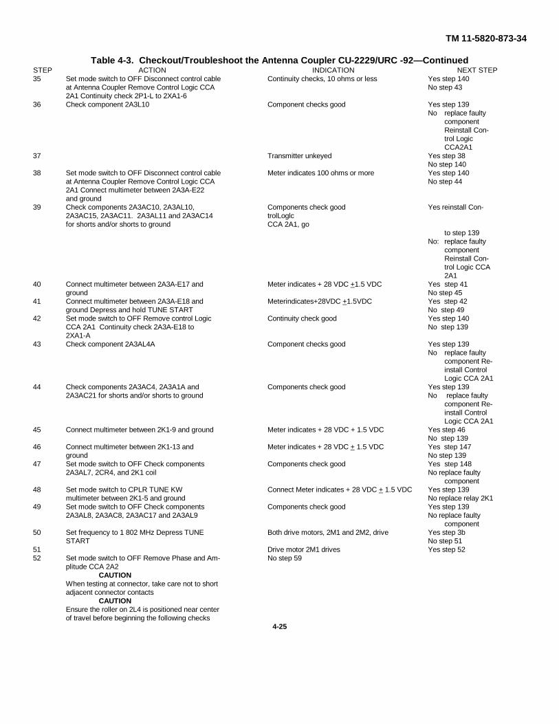
TM 11-5820-873-34
Table 4-3. Checkout/Troubleshoot the Antenna Coupler CU-2229/URC -92— ContinuedSTEP ACTION INDICATION NEXT STEP35 Set mode switch to OFF Disconnect control cable Continuity checks, 10 ohms or less Yes step 140
at Antenna Coupler Remove Control Logic CCA No step 432A1 Continuity check 2P1-L to 2XA1-6
36 Check component 2A3L10 Component checks good Yes step 139No replace faulty
componentReinstall Con-trol LogicCCA2A1
37 Transmitter unkeyed Yes step 38No step 140
38 Set mode switch to OFF Disconnect control cable Meter indicates 100 ohms or more Yes step 140at Antenna Coupler Remove Control Logic CCA No step 442A1 Connect multimeter between 2A3A-E22and ground
39 Check components 2A3AC10, 2A3AL10, Components check good Yes reinstall Con-2A3AC15, 2A3AC11. 2A3AL11 and 2A3AC14 trolLoglcfor shorts and/or shorts to ground CCA 2A1, go
to step 139No: replace faulty
componentReinstall Con-trol Logic CCA2A1
40 Connect multimeter between 2A3A-E17 and Meter indicates + 28 VDC +1.5 VDC Yes step 41ground No step 45
41 Connect multimeter between 2A3A-E18 and Meterindicates+28VDC +1.5VDC Yes step 42ground Depress and hold TUNE START No step 49
42 Set mode switch to OFF Remove control Logic Continuity check good Yes step 140CCA 2A1 Continuity check 2A3A-E18 to No step 1392XA1-A
43 Check component 2A3AL4A Component checks good Yes step 139No replace faulty
component Re-install ControlLogic CCA 2A1
44 Check components 2A3AC4, 2A3A1A and Components check good Yes step 1392A3AC21 for shorts and/or shorts to ground No replace faulty
component Re-install ControlLogic CCA 2A1
45 Connect multimeter between 2K1-9 and ground Meter indicates + 28 VDC + 1.5 VDC Yes step 46 No step 13946 Connect multimeter between 2K1-13 and Meter indicates + 28 VDC + 1.5 VDC Yes step 147
ground No step 13947 Set mode switch to OFF Check components Components check good Yes step 148
2A3AL7, 2CR4, and 2K1 coil No replace faultycomponent
48 Set mode switch to CPLR TUNE KW Connect Meter indicates + 28 VDC + 1.5 VDC Yes step 139multimeter between 2K1-5 and ground No replace relay 2K1
49 Set mode switch to OFF Check components Components check good Yes step 1392A3AL8, 2A3AC8, 2A3AC17 and 2A3AL9 No replace faulty
component50 Set frequency to 1 802 MHz Depress TUNE Both drive motors, 2M1 and 2M2, drive Yes step 3b
START No step 5151 Drive motor 2M1 drives Yes step 5252 Set mode switch to OFF Remove Phase and Am- No step 59
plitude CCA 2A2CAUTION
When testing at connector, take care not to shortadjacent connector contacts
CAUTIONEnsure the roller on 2L4 is positioned near centerof travel before beginning the following checks
4-25
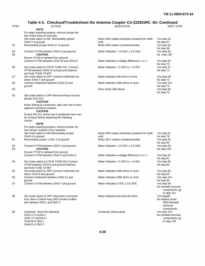
TM 11-5820-873-34
Table 4-3. Checkout/Troubleshoot the Antenna Coupler CU-2229/URC -92--ContinuedSTEP ACTION INDICATION NEXT STEP
NOTEFor steps requiring jumpers, remove jumper be-fore motor drives to end stopSet mode switch to AM Momentarily jumper Motor 2M2 rotates clockwise (viewed from shaft Yes step 532XA2-V to ground end) No step 67
53 Momentarily jumper 2XA2-17 to ground Motor 2M2 rotates counterclockwise Yes step 54No step 68
54 Connect VTVM between 2XA2-U and ground Meter indicates + 10 VDC + 0.8 VDC Yes step 5555 CAUTION No step 139
Ensure VTVM Is isolated from groundConnect VTVM between 2XA2-16 and 2XA2-U Meter indicates a voltage difference (+ or -) Yes step 56
No step 7056 Set mode switch to CPLR TUNE KW Connect Meter indicates + 3 VDC to + 5 VDC Yes step 57
VTVM between 2XA2-14 and ground Depress No step 71and hold TUNE START
57 Set mode switch to OFF Connect multimeter be- Meter indicates 200 ohms or more Yes step 58tween 2XA2-7 and ground No step 72
58 Connect multimeter between 2XA2-15 and Meter indicates 1000 ohms or more Yes step 141ground No step 74
59 Drive motor 2M2 drives Yes step 60No step 75
60 Set mode switch to OFF Remove Phase and Am-plitude CCA 2A2
CAUTIONWhen testing at connectors, take care not to shortadjacent connector contacts
CAUTIONEnsure the 2C1 sensor bar is positioned near cen-ter of travel before beginning the followingchecks
NOTEFor steps requiring jumpers, remove jumper be-fore sensor contacts micro switchesSet mode switch to AM Momentarily jumper Motor 2M1 rotates clockwise (viewed from shaft Yes step 612XA2-4 to ground end) No step 78
61 Momentarily jumper 2 XA2 -5 to ground Motor 2M 1 rotates counterclockwise Yes step 62No step 84
62 Connect VTVM between 2XA2-3 and ground Meter indicates + 10 VDC + 0.8 VDC Yes step 6363 CAUTION No step 139
Ensure VTVM Is Isolated from groundConnect VTVM between 2XA2-2 and 2XA2-3 Meter indicates a voltage difference (+ or -) Yes step 64
No step 8164 Set mode switch to CPLR TUNE KW Connect Meter indicates + 3 VDC to + 5 VDC Yes step 65
VTVM between 2XA2-6 and ground Depress No step 82and hold TUNE START
65 Set mode switch to OFF Connect multimeter be- Meter indicates 1000 ohms or more Yes step 66tween 2XA2-8 and ground No step 83
66 Connect multimeter between 2XA2-11 and Meter indicates 1000 ohms or more Yes step 141ground No step 84
67 Connect VTVM between 2XA2-T and ground Meter indicates 0 VDC + 0.5 VDC Yes step 68No reinstall removed
components, goto step 141
68 Set mode switch to OFF Disconnect connector Meter indicates less than 50 ohms Yes step69from Servo Control Assy 2A6 Connect multlm- No replace motoreter between 2M2-1 and 2M2-2 2M2 Reinstall
removedcomponents
69 Continuity check the following Continuity checks good Yes step 1422XA2-V to 2XA6-C No reinstall removed2XA2-17 to2XA6-H components, go2XA6-B to 2M2-1 to step 1392XA6-E to 2M2-2
4-26
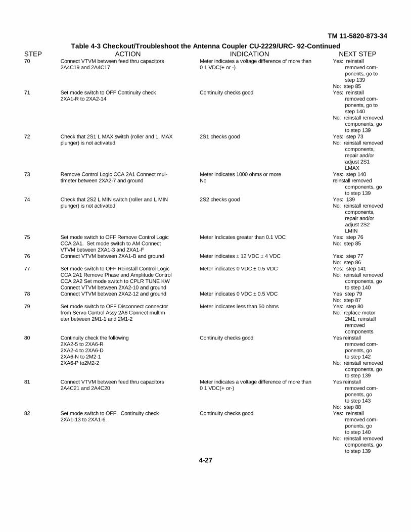
TM 11-5820-873-34Table 4-3 Checkout/Troubleshoot the Antenna Coupler CU-2229/URC- 92-Continued
STEP ACTION INDICATION NEXT STEP70 Connect VTVM between feed thru capacitors Meter indicates a voltage difference of more than Yes: reinstall
2A4C19 and 2A4C17 0 1 VDC(+ or -) removed com-ponents, go tostep 139
No: step 8571 Set mode switch to OFF Continuity check Continuity checks good Yes: reinstall
2XA1-R to 2XA2-14 removed com-ponents, go tostep 140
No: reinstall removedcomponents, goto step 139
72 Check that 2S1 L MAX switch (roller and 1, MAX 2S1 checks good Yes: step 73plunger) is not activated No: reinstall removed
components,repair and/oradjust 2S1LMAX
73 Remove Control Logic CCA 2A1 Connect mul- Meter indicates 1000 ohms or more Yes: step 140tlmeter between 2XA2-7 and ground No reinstall removed
components, goto step 139
74 Check that 2S2 L MIN switch (roller and L MIN 2S2 checks good Yes: 139plunger) is not activated No: reinstall removed
components,repair and/oradjust 2S2LMIN
75 Set mode switch to OFF Remove Control Logic Meter Indicates greater than 0.1 VDC Yes: step 76CCA 2A1. Set mode switch to AM Connect No: step 85VTVM between 2XA1-3 and 2XA1-F
76 Connect VTVM between 2XA1-B and ground Meter indicates ± 12 VDC ± 4 VDC Yes: step 77No: step 86
77 Set mode switch to OFF Reinstall Control Logic Meter indicates 0 VDC ± 0.5 VDC Yes: step 141CCA 2A1 Remove Phase and Amplitude Control No: reinstall removedCCA 2A2 Set mode switch to CPLR TUNE KW components, goConnect VTVM between 2XA2-10 and ground to step 140
78 Connect VTVM between 2XA2-12 and ground Meter indicates 0 VDC ± 0.5 VDC Yes step 79No: step 87
79 Set mode switch to OFF Disconnect connector Meter indicates less than 50 ohms Yes: step 80from Servo Control Assy 2A6 Connect multlm- No: replace motoreter between 2M1-1 and 2M1-2 2M1, reinstall
removedcomponents
80 Continuity check the following Continuity checks good Yes reinstall2XA2-5 to 2XA6-R removed com-2XA2-4 to 2XA6-D ponents, go2XA6-N to 2M2-1 to step 1422XA6-P to2M2-2 No: reinstall removed
components, goto step 139
81 Connect VTVM between feed thru capacitors Meter indicates a voltage difference of more than Yes reinstall2A4C21 and 2A4C20 0 1 VDC(+ or-) removed com-
ponents, goto step 143
No: step 8882 Set mode switch to OFF. Continuity check Continuity checks good Yes: reinstall
2XA1-13 to 2XA1-6. removed com-ponents, goto step 140
No: reinstall removedcomponents, goto step 139
4-27
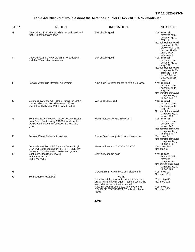
TM 11-5820-873-34Table 4-3 Checkout/Troubleshoot the Antenna Coupler CU-2229/URC- 92-Continued
STEP ACTION INDICATION NEXT STEP
83 Check that 2S3 C MIN switch is not activated and 2S3 checks good Yes: reinstallthat 2S3 contacts are open removed com-
ponents. go tostep 139
No: reinstall removedcomponents Re-place switch 2S3,perform C MINand C MAXadjustment
84 Check that 2S4 C MAX switch Is not activated 2S4 checks good Yes: reinstalland that 2S4 contacts are open removed com-
ponents. go tostep 139
No: reinstall removedcomponents Replace 2S4, per-form C MIN andC MAX adjust-ment
85 Perform Amplitude Detector Adjustment Amplitude Detector adjusts to within tolerance Yes: reinstallremoved com-ponents, go tostep 3a.
No: reinstall removedcomponents, goto step 143
86 Set mode switch to OFF Check wiring for contin- Wiring checks good Yes: reinstalluity and shorts to ground between 2J2 and removed com-2A3-E3 and between 2A3-E4 and 2XA1-B ponents, go to
step 144No: reinstall removed
components, goto step 139
87 Set mode switch to OFF. Disconnect connector Meter indicates 0 VDC ± 0.5 VDC Yes: reinstallfrom Servo Control Assy 2A6 Set mode switch removed com-to AM. Connect VTVM between 2XA6-M and ponents, goground. to step 142
No: reinstall removedcomponents, goto step 140
88 Perform Phase Detector Adjustment Phase Detector adjusts to within tolerance Yes: step 3aNo: reinstall removed
components, goto step 143
89 Set mode switch to OFF Remove Control Logic Meter indicates + 10 VDC ± 0.8 VDC Yes: step 140CCA 2A1 Set mode switch to CPLR TUNE KW No: step 90Connect VTVM between 2XA1-2 and ground
90 Continuity check the following Continuity checks good Yes: replace2A3-E8 to 2K1-12 2K1 Reinstall2K1-8 to2XA1-2 removed
componentsNo: reinstall removed
components, goto step 139
91 COUPLER STATUS FAULT indicator s lit Yes: step 92No: step 101
92 Set frequency to 15.602 NOTEIf the time delay runs out during this test, de- Yes: step 93press TUNE START again If tuning occurs the No: step 102second time the Indication is goodAntenna Coupler completes tune cycle and Yes: step 93COUPLER STATUS READY indicator illuml- No: step 102nates
4-28
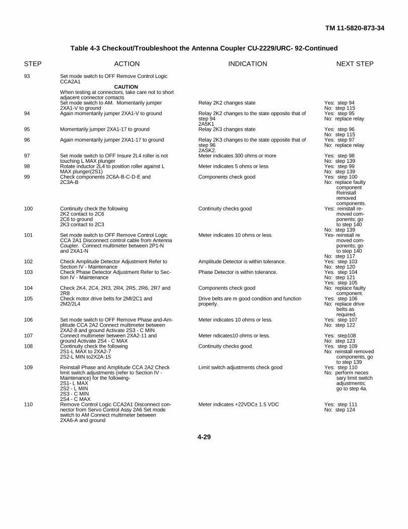
TM 11-5820-873-34
Table 4-3 Checkout/Troubleshoot the Antenna Coupler CU-2229/URC- 92-Continued
STEP ACTION INDICATION NEXT STEP
93 Set mode switch to OFF Remove Control LogicCCA2A1
CAUTIONWhen testing at connectors, take care not to shortadjacent connector contactsSet mode switch to AM. Momentarily jumper Relay 2K2 changes state Yes: step 942XA1-V to ground No: step 115
94 Again momentarily jumper 2XA1-V to ground Relay 2K2 changes to the state opposite that of Yes: step 95step 94 No: replace relay2A5K1
95 Momentarily jumper 2XA1-17 to ground Relay 2K3 changes state Yes: step 96No: step 115
96 Again momentarily jumper 2XA1-17 to ground Relay 2K3 changes to the state opposite that of Yes: step 97step 96 No: replace relay2ASK2.
97 Set mode switch to OFF Insure 2L4 roller is not Meter indicates 300 ohms or more Yes: step 98touching L MAX plunger No: step 139
98 Rotate inductor 2L4 to position roller against L Meter indicates 5 ohms or less Yes: step 99MAX plunger(2S1) No: step 139
99 Check components 2C6A-B-C-D-E and Components check good Yes: step 1002C3A-B No: replace faulty
componentReinstallremovedcomponents.
100 Continuity check the following Continuity checks good Yes: reinstall re-2K2 contact to 2C6 moved com-2C6 to ground ponents; go2K3 contact to 2C3 to step 140
No: step 139101 Set mode switch to OFF Remove Control Logic Meter indicates 10 ohms or less. Yes- reinstall re
CCA 2A1 Disconnect control cable from Antenna moved com-Coupler. Connect multimeter between 2P1-N ponents; goand 2XA1-N to step 140
No: step 117102 Check Amplitude Detector Adjustment Refer to Amplitude Detector is within tolerance. Yes: step 103
Section IV - Maintenance No: step 120103 Check Phase Detector Adjustment Refer to Sec- Phase Detector is within tolerance. Yes. step 104
tion IV - Maintenance No: step 121Yes: step 105
104 Check 2K4, 2C4, 2R3, 2R4, 2R5, 2R6, 2R7 and Components check good No: replace faulty2R8 component.
105 Check motor drive belts for 2Ml/2C1 and Drive belts are m good condition and function Yes: step 1062M2/2L4 properly. No: replace drive
belts asrequired.
106 Set mode switch to OFF Remove Phase and-Am- Meter indicates 10 ohms or less. Yes: step 107plitude CCA 2A2 Connect multimeter between No: step 1222XA2-8 and ground Activate 2S3 - C MIN
107 Connect multimeter between 2XA2-11 and Meter ndicates10 ohms or less. Yes: step108ground Activate 2S4 - C MAX No: step 123
108 Continuity check the following Continuity checks good. Yes. step 1092S1-L MAX to 2XA2-7 No: reinstall removed2S2-L MIN to2X2A-15 components, go
to step 139109 Reinstall Phase and Amplitude CCA 2A2 Check Limit switch adjustments check good Yes: step 110
limit switch adjustments (refer to Section IV - No: perform necesMaintenance) for the following- sary limit switch2S1- L MAX adjustments;2S2 - L MIN go to step 4a.2S3 - C MIN2S4 - C MAX
110 Remove Control Logic CCA2A1 Disconnect con- Meter indicates +22VDC± 1.5 VDC Yes: step 111nector from Servo Control Assy 2A6 Set mode No: step 124switch to AM Connect multimeter between2XA6-A and ground
4-29
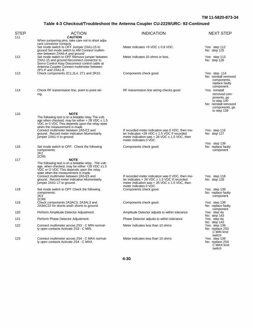
TM 11-5820-873-34Table 4-3 Checkout/Troubleshoot the Antenna Coupler CU-2229/URC- 92-Continued
STEP ACTION INDICATION NEXT STEP111 CAUTION
When jumpering pins, take care not to short adja-cent connector contactsSet mode switch to OFF Jumper 2XA1-15 to Meter indicates +9 VDC ± 0.8 VDC. Yes: step 112ground Set mode switch to AM Connect multim- No: step 125eter between 2XA6-A and ground
112 Set mode switch to OFF Remove jumper between Meter indicates 10 ohms or less. Yes: step 1132XA1-15 and ground Reconnect connector to No: step 126Servo Control Assy Disconnect control cable atAntenna Coupler Connect multimeter between2P1-P and 2XA1-8
113 Check components 2C1,2L4, 2T1 and 2R10. Components check good. Yes: step 114No: reinstall removed
components,replace faultycomponent.
114 Check RF transmission line, point to point wir- RF transmission line wiring checks good Yes: reinstalling. removed com-
ponents, goto step 140
No: reinstall removedcomponents, goto step 139
115 NOTEThe following test is on a bistable relay The volt-age when checked, may be either + 28 VDC ± 1.5VDC or 0 VDC This depends upon the relay statewhen the measurement is madeConnect multimeter between 2A5-E2 and If recorded meter indication was 0 VDC, then me- Yes: step 116ground. Record meter indication Momentarily ter Indicates +28 VDC ± 1.5 VDC If recorded No: step 127jumper 2XA1-V to ground meter indication was + 28 VDC ± 1.5 VDC, then
meter indicates 0 VDCYes: step 139
116 Set mode switch to OFF. Check the following Components check good. No: replace faultycomponents: component2K22CR5
117 NOTEThe following test is on a bistable relay. The volt-age, when checked, may be either +28 VDC ±1.5VDC or O VDC This depends upon the relaystate when the measurement is madeConnect multimeter between 2A5-E5 and If recorded meter indication was 0 VDC, then me- Yes. step 118ground. Record meter indication Momentarily ter indicates + 28 VDC ± 1.5 VDC If recorded No: step 128jumper 2XA1-17 to ground. meter indication was + 28 VDC ± 1.5 VDC, then
meter indicates 0 VDC118 Set mode switch to OFF Check the following Components check good. Yes: step 139
components: No: replace faulty2K3 component2CR6
119 Check components 2A3AC3, 2A3AL3 and Components check good. Yes: step 1392A3AC22 for shorts and/r shorts to ground. No: replace faulty
component120 Perform Amplitude Detector Adjustment. Amplitude Detector adjusts to within tolerance Yes: step 4a
No: step 143121 Perform Phase Detector Adjustment. Phase Detector adjusts to within tolerance Yes: step 4a
No: step 143122 Connect multimeter across 2S3 - C MIN normal- Meter indicates less than 10 ohms Yes: step 139
ly open contacts Activate 2S3 - C MIN. No: replace 2S3C MIN limitswitch
123 Connect multimeter across 2S4 - C MAX normal- Meter indicates less than 10 ohms Yes: step 139ly open contacts Activate 2S4 - C MAX. No: replace 2S4
C MAX limitswitch
4-30
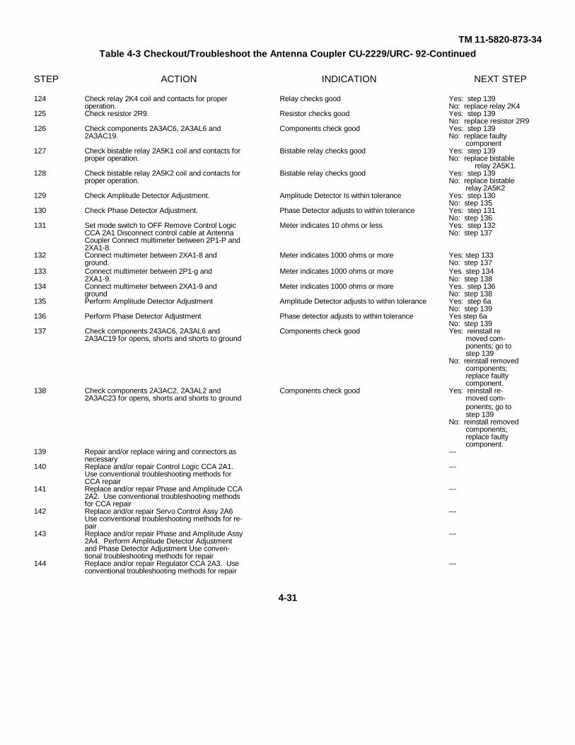
TM 11-5820-873-34Table 4-3 Checkout/Troubleshoot the Antenna Coupler CU-2229/URC- 92-Continued
STEP ACTION INDICATION NEXT STEP
124 Check relay 2K4 coil and contacts for proper Relay checks good Yes: step 139operation. No: replace relay 2K4
125 Check resistor 2R9. Resistor checks good Yes: step 139No: replace resistor 2R9
126 Check components 2A3AC6, 2A3AL6 and Components check good Yes: step 1392A3AC19. No: replace faulty
component127 Check bistable relay 2A5K1 coil and contacts for Bistable relay checks good Yes: step 139
proper operation. No: replace bistablerelay 2A5K1.
128 Check bistable relay 2A5K2 coil and contacts for Bistable relay checks good Yes: step 139proper operation. No: replace bistable
relay 2A5K2129 Check Amplitude Detector Adjustment. Amplitude Detector Is within tolerance Yes: step 130
No: step 135130 Check Phase Detector Adjustment. Phase Detector adjusts to within tolerance Yes: step 131
No: step 136131 Set mode switch to OFF Remove Control Logic Meter indicates 10 ohms or less Yes: step 132
CCA 2A1 Disconnect control cable at Antenna No: step 137Coupler Connect multimeter between 2P1-P and2XA1-8.
132 Connect multimeter between 2XA1-8 and Meter indicates 1000 ohms or more Yes: step 133ground. No: step 137
133 Connect multimeter between 2P1-g and Meter indicates 1000 ohms or more Yes step 1342XA1-9. No: step 138
134 Connect multimeter between 2XA1-9 and Meter indicates 1000 ohms or more Yes. step 136ground No: step 138
135 Perform Amplitude Detector Adjustment Amplitude Detector adjusts to within tolerance Yes: step 6aNo: step 139
136 Perform Phase Detector Adjustment Phase detector adjusts to within tolerance Yes step 6aNo: step 139
137 Check components 243AC6, 2A3AL6 and Components check good Yes: reinstall re2A3AC19 for opens, shorts and shorts to ground moved com-
ponents; go tostep 139
No: reinstall removedcomponents;replace faultycomponent.
138 Check components 2A3AC2, 2A3AL2 and Components check good Yes: reinstall re-2A3AC23 for opens, shorts and shorts to ground moved com-
ponents; go tostep 139
No: reinstall removedcomponents;replace faultycomponent.
139 Repair and/or replace wiring and connectors as ---necessary
140 Replace and/or repair Control Logic CCA 2A1. ---Use conventional troubleshooting methods forCCA repair
141 Replace and/or repair Phase and Amplitude CCA ---2A2. Use conventional troubleshooting methodsfor CCA repair
142 Replace and/or repair Servo Control Assy 2A6 ---Use conventional troubleshooting methods for re-pair
143 Replace and/or repair Phase and Amplitude Assy ---2A4. Perform Amplitude Detector Adjustmentand Phase Detector Adjustment Use conven-tional troubleshooting methods for repair
144 Replace and/or repair Regulator CCA 2A3. Use ---conventional troubleshooting methods for repair
4-31
TM 11-5820-873-34
Section IV. MAINTENANCE4-7. GeneralGeneral support maintenance of the AN/URC-92 is limitedto the replacement and/or repair of wiring and connectors,circuit card replacement and/or repair and the proceduresoutlined in this manual.4-8. Power Supply 1A6
(Fig 4-3)a. Removal.
(1) Remove transceiver top cover.(2) Remove transceiver bottom cover.(3) Remove four screws holding Synthesizer 1A4
protective cover and remove protective cover.(4) Extract Spectrum Generator 1A4A1, Low Digit
Generator 1A4A2, Translator 1A4A3, and VHF Divider1A4A4 circuit card assemblies.
(5) Remove two screws and washers (16) holdingPower Supply 1A6 to Synthesizer 1A4.
(6) Remove one screw and washer (15) mountingpower supply to chassis assembly.
(7) Remove two screws (17) mounting powersupply to rear panel.
(8) Remove six screws mounting rear panel toright and left side panels and pull away rear panel
(9) Remove four screws (1) from RegulatorAssembly 1A6A1 protective cover (2) and remove cover.
(10) Remove two standoffs (3) from RegulatorAssembly 1A6A1 (25).
(11) Remove four screws (4) and washers (5)mounting capacitors 1A6AIC5 (9) and 1A6A1C9 (10) andremove capacitors.
(12) Remove two mounting screws (21) andwashers (19 & 20) from connector 1A6XA1 (18).
(13) Extract Regulator Assembly 1A6A1 (22) fromconnector 1A6XA1 (18).
(14) Remove two mounting screws (11) andwashers (12 & 13) from terminal board 1A6TB1 (14).
NOTEReposition terminal board 1A6TB1 to accessscrews mounting Power Supply 1A6 totransformer 1A6T1.
(15) Remove four screws (8) and washers (7)mounting Power Supply 1A6 to Power Transformer 1A6T1(6) and remove Power Supply.
b. Replacement.(1) Position Power Supply 1A6 in place and
secure with four screws (8) and washers (7) to PowerTransformer 1A6 T1 (6).
(2) Position terminal board 1A6TB1 (14) in placeand secure with two mounting screws (11) and washers(12 & 13).
CAUTIONComponent side of Regulator Assemblymust face top of transceiver.
(3) Reinstall Regulator Assembly 1A6A1 (22) intoconnector 1A6XA1 (18).
(4) Position rubber support (23) betweenRegulator Assembly 1A6A1 (22) and Power Supply 1A6.
CAUTIONPositive terminals of capacitors 1A6A1C5and 1A6A1C9 must match positive markingson Regulator Board.
(5) Position capacitors 1A6A1C5 (9) and1A6A1C9 (10) and secure each with two mounting screws(4) and washers (5) through Regulator Assembly 1A6A1(22).
(6) Reinstall two mounting screws (21) andwashers (19 & 20) in connector 1A6XA1 (18).
(7) Reinstall two standoffs (3) on RegulatorAssembly 1A6A1 (22).
(8) Position Regulator Assembly 1A6A1protective cover (2) and secure with four screws (1).
(9) Position rear panel in place and secure withsix mounting screws to left and right side panels.
(10) Reinstall two power supply mounting screws(17) through rear panel.
(11) Reinstall one power supply mounting screw(15) through chassis assembly.
(12) Reinstall two power supply mounting screws(16) through Synthesizer 1A4.
CAUTIONWhen reinstalling Spectrum Generator, LowDigit Generator, Translator, and VHF Dividercircuit card assemblies, component sidemust face rear of transceiver.
(13) Reinstall Spectrum Generator 1A4A1, LowDigit Generator 1A4A2, Translator 1A4A3, and VHFDivider 1A4A4 circuit card assemblies.
(14) Position Synthesizer 1A4 protective cover inplace and secure with four mounting screws.
(15) Reinstall transceiver bottom cover.(16) Reinstall transceiver top cover.
4-9. Power Transformer (1A6T1)(Fig 4-3)
a. Removal.(1) Remove transceiver top cover(2) Remove transceiver bottom cover.(3) Remove four screws (1) from Regulator
Assembly 1A6A1 protective cover (2) and remove cover.(4) Remove two standoffs (3) from Regulator
Assembly 1A6A1 (22).(5) Remove two screws (4) and washers (5) from
capacitor 1A6A1C5 (9) and remove capacitor.(6) Remove two screws (4) and washers (5) from
capacitor 1A6A1C9 (12) and remove capacitor.(7) Remove two mounting screws (21) and
washers (19 & 20) from connector 1A6XA1 (21).4-32
TM 11-5820-873-34(8) Extract Regulator Assembly 1A6A1 (20) from
connector 1A6XA1 (18).(9) Remove two mounting screws (11) and
washers (12 & 13) from terminal board 1A6TB1 (16)NOTE
Reposition terminal board 1A6TB1 foraccess to screws mounting transformer1A6T1.
(10) Remove three screws mounting right sidepanel to front panel.
(11) Remove five screws mounting right sidepanel to chassis assembly.
(12) Remove three screws mounting right sidepanel to rear panel.
(13) Remove four screws mounting right sidepanel to Power Transformer 1A6T1 (6) and remove rightside panel
(14) Remove four screws (8) and washer (7)mounting Power Transformer 1A6T1 (6) to the PowerSupply 1A6.
(15) Record Power Transformer 1A6T1 wiring andremove Power Transformer.
b. Replacement.(1) Make proper Power Transformer wiring
connections.(2) Position Power Transformer 1A6T1 (6) in
place and install with four mounting screws (8) andwashers (7) through Power Supply 1A6.
(3) Position right side panel in place and installwith four screws to Power Transformer 1A6T1.
(4) Reinstall three mounting screws to front panel.(5) Reinstall five mounting screws to chassis
assembly.(6) Reinstall three mounting screws to rear panel.(7) Position terminal board 1A6TB1 (14) in place
and secure with two mounting screws (11) and washers(12 & 13).
CAUTIONComponents side of Regulator Assemblymust face top of transceiver
(8) Reinstall Regulator Assembly 1A6A1 (22) intoconnector 1A6XA1 (18).
(9) Position rubber support (23) betweenRegulator Assembly 1A6A1 (22) and Power Supply 1A6.
CAUTIONPositive terminals of capacitors 1A6A1C5and 1A6A1C9 must match positive markingson Regulator Board
(10) Position capacitors 1A6A1C5 (9) and1A6A1C9 (10) and secure with four mounting screws (4)and washers (5) through Regulator Assembly 1A6A1 (22).
(11) Reinstall two mounting screws (21) andwashers (19 & 20) in connector 1A6XA1 (18).
(12) Reinstall two standoffs (3) on RegulatorAssembly 1A6A1 (22).
(13) Position protective cover (2) in place andsecure with four mounting screws (1)
(14) Reinstall transceiver bottom cover(15) Reinstall transceiver top cover.
4-10. Regulator Assembly(Fig 4-3)
a Removal.(1) Remove transceiver top cover(2) Remove four screws (1) from Regulator
Assembly 1A6A1 protective cover (2) and remove cover.(3) Remove two standoffs (3) from Regulator
Assembly 1A6A1 (22).(4) Remove four screws (4) and washers (5)
mounting capacitors 1A6A1C5 (9) and 1A6A1C9 (10) andremove capacitors.
(5) Remove two mounting screws (21) andwashers (19 & 20) from connector 1A6XA1 (18)
(6) Extract Regulator Assembly 1A6A1 (22) fromconnector 1A6XA1 (18)
b ReplacementCAUTION
Component side of Regulator Assemblymust face top of transceiver.
(1) Reinstall Regulator Assembly 1A6A1 (22) intoconnector 1A6XA1 (18).
(2) Position rubber support (23) betweenRegulator Assembly 1A6A1 (22) and Power Supply 1A6.
CAUTIONPositive terminals of capacitors 1A6A1C5and 1A6A1C9 must match positive markingson Regulator Board.
(3) Position capacitors 1A6AlC5 (9) and 1A6A1C9(10) and secure each with two mounting screws (4) andwashers (5) through Regulator Assembly 1A6A1 (22).
(4) Reinstall two mounting screws (21) andwashers (19 & 20) in connector 1A6XA1 (18).
(5) Reinstall two standoffs (3) on RegulatorAssembly 1A6A1 (22).
(6) Position Regulator Assembly 1A6A1protective cover (2) and secure with four screws (1).
(7) Reinstall transceiver top cover.4-11. Receiver/Exciter Mother Board
a. Removal.(1) Remove transceiver top cover.(2) Remove transceiver bottom cover.(3) Remove four mounting screws from
Receiver/Exciter top protective plate and remove plate.(4) Extract Audio 1A3A4, Sideband Generator
1A3A3, IF Filter 1A3A2 and VHF Mixer 1A3A1 circuit cardassemblies.
(5) Extract protective card shield(6) Remove four mounting screws and washers
4-33
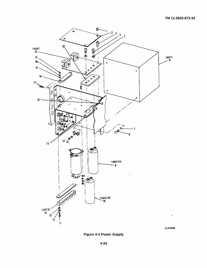
TM 11-5820-873-34
Figure 4-3 Power Supply
4-34
TM 11-5820-873-34
from Receiver/Exciter bottom shield and remove bottomshield.
(7) Disconnect connector 1A1P2 from connector1A3A5J5.
(8) Remove four mounting screws fromReceiver/Exciter Mother Board 1A3A5.
(9) Remove two mounting screws and washersfrom Receiver/Exciter Coax Bracket and remove bracket.
(10) Label all wiring connections.(11) Unsolder wires and remove Receiver/Exciter
Mother Board 1A3A5.b. Replacement.
(1) Make necessary wiring connections.NOTE
When securing Receiver/Exciter MotherBoard in place, two loop clamps are used toretain wiring.
(2) Position Receiver/Exciter Mother Board1A3A5 in place and secure with four mounting screws.
(3) Position Receiver/Exciter Coax Bracket inplace and secure with two mounting screws and washers.
(4) Reconnect connector 1A1P2 to connector1A3A5J5.
(5) Position Receiver/Exciter bottom shield inplace and secure with four mounting screws and washers.
NOTEWhen installing Audio, Sideband Generator,IF Filter, and VHF Mixer circuit cardassemblies, components side must facefront of transceiver.
(6) Reinstall Audio 1A3A4, Sideband Generator1A3A3, IF Filter 1A3A2, VHF Mixer 1A3A1 circuit cardassemblies.
(7) Reinstall protective card shield.(8) Position Receiver/Exciter top protective plate
in place and secure with four screws.(9) Replace transceiver bottom cover.(10) Replace transceiver top cover.
4-12. Synthesizer Mother Boarda. Removal.
(1) Remove transceiver top cover.(2) Remove transceiver bottom cover.(3) Remove four mounting screws from
Synthesizer top protective plate and remove plate.(4) Remove six mounting screws attaching front
panel to transceiver and swing front panel downward.(5) Remove four mounting screws and washers
from VCO 1A4A5 and extract VCO.(6) Extract Spectrum Generator 1A4A1, Low Digit
Generator 1A4A2, Translator 1A4A3, and VHF Divider1A4A4 circuit card assemblies.
(7) Remove four mounting screws and washersfrom Snythesizer bottom shield and remove shield (8)
Disconnect connector 1A1P3 from connector 1A4A6J1.(9) Remove four mounting screws from
Synthesizer Mother Board 1A4A6.(10) Remove two mounting screws and washers
from Snythesizer coax bracket and remove bracket.(11) Label all wiring connections.(12) Unsolder wires and remove Synthesizer
Mother Board 1A4A6.b. Replacement
(1) Make necessary wiring connections.(2) Position Synthesizer Coax Bracket m place
and secure with two mounting screws and washers.(3) Position Synthesizer Mother Board 1A4A6 and
secure with four mounting screws.(4) Reconnect connector 1A1P3 to connector
1A4A6J1.(5) Position Synthesizer bottom shield in place
and secure with four mounting screws.NOTE
When installing Spectrum Generator, LowDigit Generator, Translator, and VHF Dividercircuit card assemblies, component sidemust face rear of transceiver.
(6) Reinstall Spectrum Generator 1A4A1, LowDigit Generator 1A4A2, Translator 1A4A3, and VHFDivider 1A4A4 circuit card assemblies.
(7) Reinstall VCO 1A4A5 and secure with fourmounting screws and washers.
(8) Position Front Panel in place and secure withsix mounting screws.
(9) Position Synthesizer top protective plate inplace and secure with four mounting screws.
(10) Reinstall transceiver bottom cover.(11) Reinstall transceiver top cover.
4-13. Filter Module(Fig 4-4)
a. Removal.(1) Remove transceiver top cover.(2) Remove transceiver bottom cover.(3) Disconnect connector 1A8P2 from connector
1A5J1(4) Disconnect connector 1A8P4 from connector
1A5J2.(5) Disconnect connector 1A3P4 from connector
1A5J3.(6) Disconnect connector 1A8P5 from connector
1A5J4.(7) Remove two mounting screws (3) from filter
support bracket (2).(8) Remove two mounting screws (6) and washers
(5) from filter assembly cradle (4) and lift out FilterModule 1A5 (1).
b. Replacement.
4-35
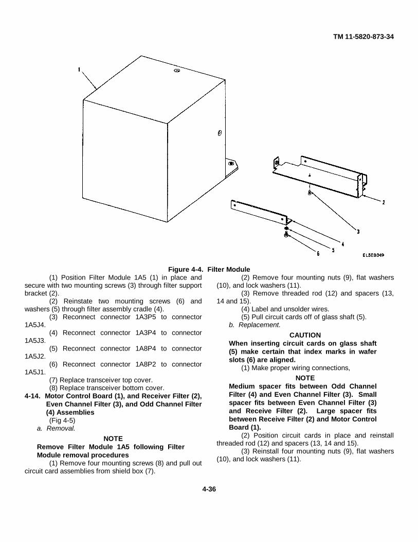
TM 11-5820-873-34
Figure 4-4. Filter Module(1) Position Filter Module 1A5 (1) in place and
secure with two mounting screws (3) through filter supportbracket (2).
(2) Reinstate two mounting screws (6) andwashers (5) through filter assembly cradle (4).
(3) Reconnect connector 1A3P5 to connector1A5J4.
(4) Reconnect connector 1A3P4 to connector1A5J3.
(5) Reconnect connector 1A8P4 to connector1A5J2.
(6) Reconnect connector 1A8P2 to connector1A5J1.
(7) Replace transceiver top cover.(8) Replace transceiver bottom cover.
4-14. Motor Control Board (1), and Receiver Filter (2),Even Channel Filter (3), and Odd Channel Filter(4) Assemblies(Fig 4-5)
a. Removal.NOTE
Remove Filter Module 1A5 following FilterModule removal procedures
(1) Remove four mounting screws (8) and pull outcircuit card assemblies from shield box (7).
(2) Remove four mounting nuts (9), flat washers(10), and lock washers (11).
(3) Remove threaded rod (12) and spacers (13,14 and 15).
(4) Label and unsolder wires.(5) Pull circuit cards off of glass shaft (5).
b. Replacement.CAUTION
When inserting circuit cards on glass shaft(5) make certain that index marks in waferslots (6) are aligned.
(1) Make proper wiring connections,NOTE
Medium spacer fits between Odd ChannelFilter (4) and Even Channel Filter (3). Smallspacer fits between Even Channel Filter (3)and Receive Filter (2). Large spacer fitsbetween Receive Filter (2) and Motor ControlBoard (1).
(2) Position circuit cards in place and reinstallthreaded rod (12) and spacers (13, 14 and 15).
(3) Reinstall four mounting nuts (9), flat washers(10), and lock washers (11).
4-36
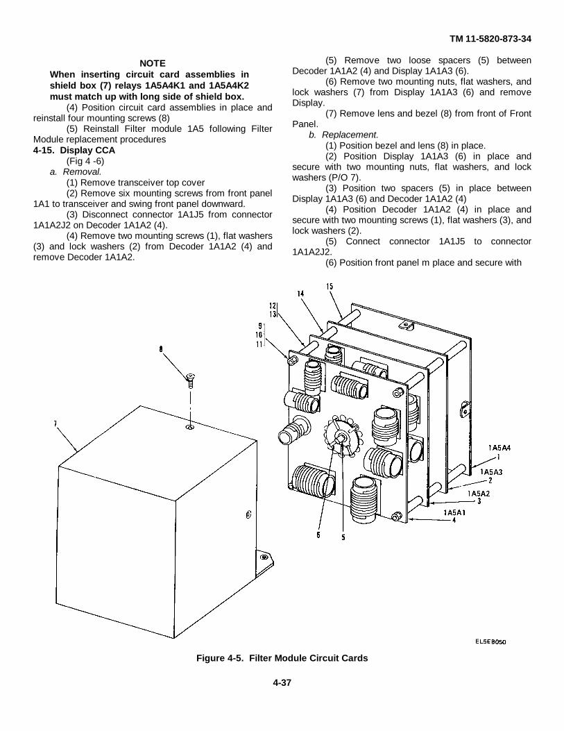
TM 11-5820-873-34
NOTEWhen inserting circuit card assemblies inshield box (7) relays 1A5A4K1 and 1A5A4K2must match up with long side of shield box.
(4) Position circuit card assemblies in place andreinstall four mounting screws (8)
(5) Reinstall Filter module 1A5 following FilterModule replacement procedures4-15. Display CCA
(Fig 4 -6)a. Removal.
(1) Remove transceiver top cover(2) Remove six mounting screws from front panel
1A1 to transceiver and swing front panel downward.(3) Disconnect connector 1A1J5 from connector
1A1A2J2 on Decoder 1A1A2 (4).(4) Remove two mounting screws (1), flat washers
(3) and lock washers (2) from Decoder 1A1A2 (4) andremove Decoder 1A1A2.
(5) Remove two loose spacers (5) betweenDecoder 1A1A2 (4) and Display 1A1A3 (6).
(6) Remove two mounting nuts, flat washers, andlock washers (7) from Display 1A1A3 (6) and removeDisplay.
(7) Remove lens and bezel (8) from front of FrontPanel.
b. Replacement.(1) Position bezel and lens (8) in place.(2) Position Display 1A1A3 (6) in place and
secure with two mounting nuts, flat washers, and lockwashers (P/O 7).
(3) Position two spacers (5) in place betweenDisplay 1A1A3 (6) and Decoder 1A1A2 (4)
(4) Position Decoder 1A1A2 (4) in place andsecure with two mounting screws (1), flat washers (3), andlock washers (2).
(5) Connect connector 1A1J5 to connector1A1A2J2.
(6) Position front panel m place and secure with
Figure 4-5. Filter Module Circuit Cards
4-37
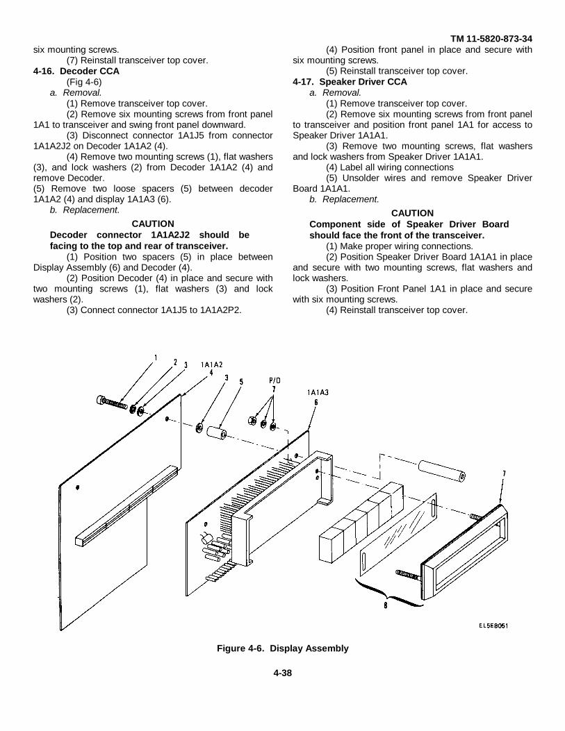
TM 11-5820-873-34six mounting screws.
(7) Reinstall transceiver top cover.4-16. Decoder CCA
(Fig 4-6)a. Removal.
(1) Remove transceiver top cover.(2) Remove six mounting screws from front panel
1A1 to transceiver and swing front panel downward.(3) Disconnect connector 1A1J5 from connector
1A1A2J2 on Decoder 1A1A2 (4).(4) Remove two mounting screws (1), flat washers
(3), and lock washers (2) from Decoder 1A1A2 (4) andremove Decoder.(5) Remove two loose spacers (5) between decoder1A1A2 (4) and display 1A1A3 (6).
b. Replacement.CAUTION
Decoder connector 1A1A2J2 should befacing to the top and rear of transceiver.
(1) Position two spacers (5) in place betweenDisplay Assembly (6) and Decoder (4).
(2) Position Decoder (4) in place and secure withtwo mounting screws (1), flat washers (3) and lockwashers (2).
(3) Connect connector 1A1J5 to 1A1A2P2.
(4) Position front panel in place and secure withsix mounting screws.
(5) Reinstall transceiver top cover.4-17. Speaker Driver CCA
a. Removal.(1) Remove transceiver top cover.(2) Remove six mounting screws from front panel
to transceiver and position front panel 1A1 for access toSpeaker Driver 1A1A1.
(3) Remove two mounting screws, flat washersand lock washers from Speaker Driver 1A1A1.
(4) Label all wiring connections(5) Unsolder wires and remove Speaker Driver
Board 1A1A1.b. Replacement.
CAUTIONComponent side of Speaker Driver Boardshould face the front of the transceiver.
(1) Make proper wiring connections.(2) Position Speaker Driver Board 1A1A1 in place
and secure with two mounting screws, flat washers andlock washers.
(3) Position Front Panel 1A1 in place and securewith six mounting screws.
(4) Reinstall transceiver top cover.
Figure 4-6. Display Assembly
4-38
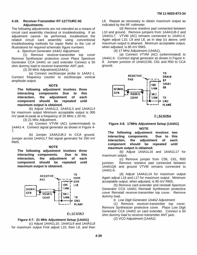
TM 11-5820-873-34
4-18. Receiver-Transmitter RT-1277/URC-92Adjustments.
The following adjustments are not intended as a means ofcircuit card assembly checkout or troubleshooting. If anadjustment cannot- be performed, troubleshoot therelated circuit card assembly using conventionaltroubleshooting methods for repair Refer to the List ofIllustrations for required schematic figure numbers
a. Spectrum Generator 1A4A1 Adjustment.(1) Remove receiver-transmitter top cover
Remove Synthesizer protective cover Place SpectrumGenerator CCA 1A4A1 on card extender Connect a 50ohm dummy load to receiver-transmitter ANT jack.
(2) 20 MHz Adjustment(1A4A1).(a) Connect oscilloscope probe to 1A4A1-1.
Connect frequency counter to oscilloscope verticalamplitude output.
NOTEThe following adjustment involves threeinteracting components Due to thisinteraction, the adjustment of eachcomponent should be repeated untilmaximum output is obtained.
(b) Adjust 1A4A1L2, 1A4A1L3 and 1A4A1L4for maximum output Minimum acceptable output is 300mV peak-to-peak at a frequency of 20 MHz ± 20 Hz.
(3) 21 Mhz Adjustment.(a) Connect VTVM (AC) (unterminated) to
1A4A1-4. Connect signal generator as shown in Figure 4-7.
(b) Jumper 1A4A1U8-2 to CCA ground.Jumper across 1A4A1L7 Set signal generator for 250 mVRMS.
NOTEThe following adjustment involves threeinteracting components. Due to thisinteraction, the adjustment of eachcomponent should be repeated untilmaximum output is obtained.
Figure 4-7. 21 MHz Adjustment Setup (1A4A1)(c) Adjust 1A4A1L10, 1A4A1L9 and 1A4A1L8
for maximum output First adjust L10, then L9, and then
L8. Repeat as necessary to obtain maximum output asindicated by the RF voltmeter.
(d) Remove resistive pad connected betweenL10 and ground. Remove jumpers from 1A4A1U8-2 and1A4A1L7. VTVM (AC) remains connected to 1A4A1-4.Again adjust L10, L9 and L8, as in step (c) above, untilmaximum output is attained. Minimum acceptable output,when adjusted, is 85 mV RMS.
(4) 17 MHz Adjustment (1A4A1).(a) Connect VTVM (AC) (unterminated) to
1A4A1-6. Connect signal generator as shown in Figure 4-8. Jumper junction of 1A4A1C56, C61 and R50 to CCAground.
Figure 4-8. 17MHz Adjustment Setup (1A4A1)NOTE
The following adjustment involves twointeracting components. Due to thisinteraction, the adjustment of eachcomponent should be repeated untilmaximum output is obtained.
(b) Adjust 1A4A1L16 and 1A4A1L17 formaximum output.
(c) Remove jumper from C56, C61, R50junction. Remove resistive pad connected between1A4A1Q6 and ground VTVM remains connected to1A4A1-6.
(d) Adjust 1A4A1L14 for maximum outputAgain adjust L16 and L17 for maximum output. Minimumacceptable output, when adjusted, is 90 mV RMS.
(5) Remove card extender and reinstall SpectrumGenerator CCA 1A4A1 Reinstall Synthesizer protectivecover Reinstall receiver-transmitter top cover. Removedummy load.
b. Low Digit Generator 1A4A2 Adjustment.(1) Remove receiver-transmitter top cover.
Remove Synthesizer protective cover. Place Low DigitGenerator CCA 1A4A2 on card extender. Connect a 50ohm dummy load to receiver-transmitter ANT jack.
(2) VCO Adjustment (1A4A2)
4-39
TM 11-5820-873-34
(a) Connect VTVM between 1A4A2-TP3 andground.
NOTEThe following two steps involve twointeracting components. Due to this, theadjustments should be worked together forthe desired output.
(b) Set 100 Hz, 1 KHz and 10 KHz to 5 Adjust1A4A2L3 for a VTVM indication of 1 95 VAC ± 0 25 VAC.
(c) Set 10 KHz to 0 Adjust 1A4A2C8 for aVTVM indication of 1.95 VAC ± 0.25 VAC.
(3) Remove card extender and reinstall Low DigitGenerator CCA 1A4A2. Reinstall Synthesizer protectivecover. Reinstall receiver-transmitter top cover. Removedummy load.
c. Translator 1A4A3 Adjustment.(1) Remove receiver-transmitter top cover
Remove Synthesizer protective cover. Place Translator1A4A3 on card extender. Connect a 50 ohm dummy loadto receiver-transmitter ANT jack.
(2) 21 MHz Adjustment (1A4A3).(a) Connect oscilloscope to 1A4A3-TP4. Set
front panel VFO PULL control to in position.(b) Adjust 1A4A3-L13 for maximum output.
Minimum acceptable output is 800 mV peak-to-peak at a0.0476 usec repetition rate.
(3) VFO Adjustment(a) Connect oscilloscope to 1A4A3-TP4.
Connect frequency counter to oscilloscope verticalamplitude output. Connect VTVM (AC) between 1A4A3-Aand ground. Pull VFO PULL control to its out position.
(b) Rotate VFO PULL control for a VTVMindication of 7.6 VDC. Observe oscilloscope and adjust1A4A3L23 until an oscillation is indicated on the scope.
(c) Continue to adjust L23 in the samedirection and note adjustment range until oscillation stops.Adjust L23 to approximate midpoint of availableadjustment range.
NOTEIf the following indication cannot beachieved, a slight readjustment of L23 isacceptable to obtain the correct frequencycount.
(d) Adjust 1A4A3L22 for a frequency counterindication of 21 MHz ± 100 Hz. Oscilloscope shouldindicate a minimum sine wave of 700 mV peak to peak.
(4) 19.45 MHz Adjustment (1A4A3)(a) Remove Low Digit Generator CCA 1A4A2.
Connect VTVM (AC) 1A4A3U3-6. Jumper 1A4A3U1-2 toCCA ground. Connect signal generator as shown inFigure 4-9.
Figure 4-9. 19.45 MHz Adjustment Setup #1 (1A4A3)NOTE
As adjustment progresses in the followingstep, reduce signal generator output level tomaintain VTVM indication below 100 mVRMS.
(b) Using frequency counter, set signalgenerator for 19 45 MHz Set signal generator level to 250mV RMS Adjust 1A4A3L3 and 1A4A3L5 for maximumVTVM indication.
(c) Connect signal generator as shown inFigure 4-10.
Figure 4-10. 19.45MHz Adjustment Setup #2(1A4A3)NOTE
The following adjustment involves twointeracting components. Due to thisinteraction, the adjustment of eachcomponent should be repeated untilmaximum output is obtained.
NOTEAs adjustment progresses in the followingstep, reduce signal generator output level tomaintain RF voltmeter indication below 100mV RMS.
(d) Adjust 1A4A3L2 and then 1A4A3L3 formaximum VTVM indication.
(e) Connect signal generator as shown inFigure 4-11.
4-40

TM 11-5820-873-34
Figure 4-11. 19.45 MHz Adjustment Setup #3 (1A4A3)NOTE
The following adjustment involves threeinteracting components Due to thisinteraction the adjustment of eachcomponent should be repeated untilmaximum output is obtained
NOTEAs adjustment progresses in the followingstep, reduce signal generator output level tomaintain VTVM indication below 100 mVRMS.
(f) Adjust 1A4A3L1, then 1A4A3L2 and then1A4A3L3 for maximum VTVM Indication.
(g) Remove Isolation pad connected betweenL1 and ground Remove jumper from 1A4A3U1-2.Reinstall Low Digit Generator CCA 1A4A2 Connect VTVM(AC) between 1A4A3U3-1 and ground Connect RFvoltmeter to 1A4A3-TP1 using a 50 ohm termination.
NOTEThe following adjustment involves fourinteracting components Due to thisinteraction the adjustment of eachcomponent should be repeated untilmaximum output is obtained.
(h) Carefully readjust L1, L2, L3, and L5 formaximum VTVM indication.
(5) 2nd Local Oscillator Adjustment(a) Connect oscilloscope to 1A4A3-11.
Ground scope to CCA ground Connect frequency counterto oscilloscope vertical amplitude output.
(b) Adjust 1A4A3L25 to approximately themidpoint of its adjustment range. Adjust 1A4A3L17 for80.75 MHz. Readjust L25 for maximum output Minimumacceptable output is 300 mV peak-to-peak at 80.75 MHz ±4 KHz.
(6) 100 75 MHz Bandpass Filter Adjustment(1A4A3).
(a) Jumper junction of 1A4A3Q8 gate #1 andR70 to CCA ground. Connect VTVM (AC) (w/50 ohmtermination) to 1A4A3-TP3 Using frequency counter setsignal generator to 100.75 MHz. Connect signalgenerator as shown in Figure 4-12.
Figure 4-12. 100.75 MHz Bandpass Filter AdjustmentSetup #1
(b) Adjust 1A4A3L21 for maximum output.(c) Connect signal generator as shown in
Figure 4-13. Frequency setting remains at 100.75 MHz.
Figure 4-13. 100.75 MHz Bandpass Filter AdjustmentSetup #2
NOTEThe following adjustment involves twointeracting components. Due to thisInteraction the adjustment of eachcomponent should be repeated untilmaximum output is obtained.
(d) Adjust 1A4A3L36 and then L21 formaximum VTVM indication.
(e) Connect signal generator as shown inFigure 4-14. Frequency setting remains at 100.75 MHz.
Figure 4-14. 100.75 MHz Bandpass Adjustment Setup#3
4-41
TM 11-5820-873-34
NOTEThe following adjustment involves threeinteracting components. Due to thisinteraction the adjustment of eachcomponent should be repeated untilmaximum output is obtained.
(f) Adjust 1A4A3L20, then L36, and then L21for maximum RF voltmeter indication.
(g) Remove isolation pad connected betweenL20 and ground. Remove jumper from between junctionof 1A4A3Q8, R71 and ground.
NOTEThe following adjustment involves threeinteracting components Due to thisinteraction the adjustment of eachcomponent should be repeated untilmaximum output is obtained.
(h) Carefully readjust L20, L36 and L21 formaximum RF voltmeter indication.
(7) 81.25 MHz Bandpass Filter Adjustment(1A4A3)
(a) Jumper Junction of 1A4A3Q11 gate # andR14 to CCA ground. Connect VTVM (AC) to 1A4A3-TP2.Using frequency counter, set signal generator to 81.25MHz. Set signal generator output level to 250 mV.Connect signal generator as shown in Figure 4-15.
Figure 4-15. 81.25 MHz Bandpass Filter AdjustmentSetup #1.
(b) Adjust 1A4A3L8 for maximum RFvoltmeter indication.
(c) Connect signal generator as shown infigure 4-16. Frequency setting remains at 81.25 MHz.
NOTEThe following adjustment involves twointeracting components. Due to thisinteraction the adjustment of eachcomponent should be repeated untilmaximum output is obtained.
(d) Adjust 1A4A3L7 and then L8 for maximumVTVM indication.
(e) Remove isolation pad connected betweenL7 and ground. Remove jumper from between junction of1A4A3Q11, R14 and ground.
Figure 4-16. 81.25 MHz Bandpass Filter AdjustmentSetup #2
NOTEThe following adjustment involves twointeracting components. Due to thisinteraction the adjustment of eachcomponent should be repeated untilmaximum output is obtained.
(f) Carefully readjust L7 and L8 for maximumVTVM indication. Minimum acceptable output is 40 mV.
(8) To adjust Output Level, connect oscilloscopeto 1A4A3-15. Set front panel FREQUENCY switches to29.9999 MHz. Adjust 1A4A3R54 for 600 mV peak-to-peak.
(9) Remove card extender and reinstall Translator1A4A3. Reinstall Synthesizer protective cover. Reinstallreceiver-transmitter top cover. Remove dummy load.
d. VHF VCO CCA 1A4A 5Adjustment.(1) Remove receiver-transmitter top cover.
Remove Synthesizer protective cover Remove receivertransmitter bottom cover. Remove six front panelmounting screws. Lay front panel forward. Connect a 50ohm dummy load to receiver-transmitter ANT jack. (SeeFig 4-17 for adjustment points.) Remove VHF DividerCCA 1A4A4.
(2) Band "O" Adjustment(a) Connect frequency counter to 1st Local
Oscillator output 1A4A5J1 Inject + 1.95 VDC, from abench power supply, at 1A4A5-4.
(b) Set front panel 10 MHz and 1 MHzfrequency selectors to 0. Adjust 1A4A5L1 for 91.75 ± 0.2MHz.
(c) Set front panel 1 MHz frequency selectoronly, to 9. Adjust 1A4A5C16 for 100.75 ± 0.75 MHz.
(d) Repeat steps (b) and (c) above until bothfrequency adjustments are within tolerancesimultaneously.
(3) Band "1" Adjustment(a) Connect frequency counter to 1st Local
Oscillator output 1A4A5J1. Inject +1.95 VDC, from abench power supply, at 1A4A5-4.
(b) Set front panel 10 MHz frequency selectorto
4-42
TM 11-5820-873-34
Figure 4-17. VHF VCO CCA Adjustment Points
1. Set front panel 1 MHz frequency selector to 0 Adjust1A4A5L4 for 101.75 ± 0.2 MHz.
(c) Set front panel 1 MHz frequency selectoronly to 9 Adjust 1A4A5C27 for 110.75 ± 0.75 MHz.
(d) Repeat step (b) and (c) above until bothfrequency adjustments are within tolerancesimultaneously.
(4) Band "2" Adjustment(a) Connect frequency counter to 1st Local
Oscillator output 1A4A5J1. Inject + 1.95 VDC, from abench power supply, at 1A4A5-4.
(b) Set front panel 10 MHz frequencyselector to 2. Set front panel 1 MHz frequency selectorto 0. Adjust 1A4A5L7 for 111.75 ± 0.2 MHz
(c) Set front panel 1 MHz frequency selectoronly, to 9 Adjust 1A4A5C38 for 120.75 ± 0.75 MHz.
(d) Repeat steps (b) and (c) above until bothfrequency adjustments are within tolerancesimultaneously.
(5) 1st Local Oscillator Output Level(a) Connect VTVM (AC) (w/50 ohm
termination) to 1st Local Oscillator output 1A4A5-J1.
Inject + 1.95 VDC, from a bench power supply, at1A4A5-4. Connect a 47 ohm, 1/2 or 1/4 watt, resistorbetween 1A4A5-2 and ground.
(b) Set front panel 10 MHz frequencyselector to 1. Set front panel 1 MHz frequency selectorto 6. Adjust 1A4A5L12 for approximately 225 mV RMS.Minimum acceptable output is 100 mV RMS.
(c) Record VTVM reading 1 MHz frequencyselector set to 0. Record RF voltmeter reading with 10MHz frequency selector set to 2 and 1 MHz frequencyselector set to 9.
(d) Readjust 1A4A5L12 as necessary so theVTVM readings are within 3 dB of each other in steps(b) and (c) above.
(e) Remove 47 ohm resistor between1A4A5-2 and ground.
(6) Remove dummy load. Reinstall VHFDivider CCA 1A4A4. Reinstall Synthesizer protectivecover. Reinstall receiver-transmitter bottom cover.Reinstall receiver-transmitter top cover. Reinstall frontpanel.
4-43
TM 11-5820-873-34
e. VHF Mixer CCA 1A3AI Adjustments.(1) Remove receiver-transmitter top cover
Remove Receiver/Exciter protective cover. Place VHFMixer CCA on card extender. Connect RF signalgenerator to ANT jack 1A8J1 Set RF signal generator to16 MHz.
(2) Set front panel frequency switches to 16 MHz.Set mode switch to USB Adjust front panel RF GAINcontrol for an S9 reading on the ANTENNA COUPLERCONTROL S meter 1A2M1.
(3) Set RF signal generator level to 10 mV andadjust signal generator frequency until a tone is heardfrom the receiver speaker.
(4) Alternately adjust 1A3A1C41 and C44 for amaximum peak on S meter 1A2M1.
(5) Alternately adjust 1A3AlT7 and T8 for amaximum peak on S meter 1A2M1.
(6) Readjust 1A3A1T7 and 1A3A1C44 formaximum S meter, 1A2M1, peak.
(7) Remove card extender and install VHF MixerCCA 1A3A1 Reinstall Receiver/Exciter protective cover.Reinstall receiver-transmitter top cover.
f. IF/Filter CCA 1A3A2Adjustment.(1) Remove receiver-transmitter top cover
Remove Receiver/Exciter protective cover. PlaceIF/Filter CCA on card extender Connect RF signalgenerator to ANT jack 1A8J1. Set RF signal generator to16 MHz.
(2) Set front panel frequency switches to 16 MHz.Set mode switch to USB. Adjust front panel RF GAINcontrol for an S9 reading on the ANTENNA COUPLERCONTROL S meter 1A2M1.
(3) Set RF signal generator level to 10 mV andadjust signal generator frequency until a tone is heardfrom the receiver speaker.
(4) Alternately adjust 1A3A2L3 and L4 for amaximum peak on S meter 1A2M1.
(5) Remove card extender and reinstall IF/FilterCCA 1A3A2. Reinstall Receiver/Exciter protective cover.Reinstall receiver-transmitter top cover.
g. Sideband Generator CCA 1A3A3 Adjustment.(1) Remove receiver-transmitter top cover
Remove Receiver/Exciter protective cover. Place Side-band Generator CCA 1A3A3 on card extender. Connecta 50 ohm dummy load to ANT jack 1A8J1. ConnectVTVM (AC) across the dummy load.
(2) Balanced Modulator Tuning.(a) Rotate 1A3A3R34 fully counterclockwise.
Then turn 1A3A3R34 approximately 8 turns clockwise Setfront panel XMT GAIN fully counterclockwise. Set modeswitch to USB.
(b) Using microphone, key transmitter andobserve VTVM. With transmitter keyed, adjust 1A3A3T1for maximum output reading on VTVM.
(c) Remove card extender and reinstallSideband Generator CCA 1A3A3. Rotate XMIT GAINcontrol fully counterclockwise Set mode switch to USB.
(d) Alternately adjust 1A3A3R34 and1A3A3C26 for minimum output reading on VTVM.
(3) ALC Adjustment Set front panel frequencyswitches to 16 MHz. Set mode switch to CW. Keytransmitter and adjust 1A3A3R55 for 71 volts RMS outputon VTVM.
(4) ACC Adjustment Set mode switch to AM.Adjust 1A3A3R18 for 42 volts RMS output on VTVM.
(5) Remove card extender and reinstall SidebandGenerator CCA 1A3A3. Reinstall Receiver/Exciterprotective cover. Reinstall receiver-transmitter top cover.Remove dummy load.4-19. Antenna Coupler CU-2229/URC-92 AdjustmentsThe following adjustments are not intended as a means ofcheckout or troubleshooting. If an adjustment cannot beperformed, troubleshoot using conventionaltroubleshooting methods. Refer to List of Illustrations forrequired schematic figure numbers.
a. C MAX/C MIN Limit Switch Adjustments (Fig 4-18)(1) Remove case from Antenna Coupler CU-
2229/URC-92. Remove Phase and Amplitude ControlCCA 2A2. Remove 2M1/2C1 drive belt (2).
(2) Connect multimeter between 2XA2-11 andchassis ground. Rotate capacitor shaft (3)counterclockwise (viewed from pulley end) until shaft justbegins to leave capacitor end plate.
NOTEShaft will rotate more freely at the pointwhere it begins to leave the capacitor endplate
Rotate shaft (3) clockwise (viewed from pulley end) twocomplete turns
(3) Adjust C MAX plunger (1) to activate C MAX2S4 (meter indicates short) at this shaft position.
(4) Connect multimeter between 2XA2-8 andchassis ground. Rotate shaft (3) clockwise (viewed frompulley end) 15 complete turns.
(5) Adjust C MIN plunger (4) to activate C MIN2S3 (meter indicates short) at this shaft position.
(6) Disconnect multimeter and reinstall 2M1/2C1drive belt. Reinstall Phase and Amplitude Control CCA2A2. Reinstall antenna coupler in case.
b. L MAX and L MIN Limit Switch Adjustments.(Fig 4-19)(1) Remove case from Antenna Coupler CU-
2229/URC-92.(2) Connect multimeter between L MAX plunger.(3) and chassis ground Rotate inductor to move
roller (2) in contact with L MAX plunger. Stop whenroller/plunger contact causes meter to indicate a short.
(3) Check the distance from the roller to the end
4-44
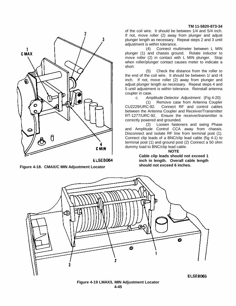
TM 11-5820-873-34
Figure 4-18. CMAX/C MIN Adjustment Locator
of the coil wire. It should be between 1/4 and S/4 inch.If not, move roller (2) away from plunger and adjustplunger length as necessary. Repeat steps 2 and 3 untiladjustment is within tolerance.
(4) Connect multimeter between L MINplunger (1) and chassis ground. Rotate inductor tomove roller (2) in contact with L MIN plunger. Stopwhen roller/plunger contact causes meter to indicate ashort.
(5) Check the distance from the roller tothe end of the coil wire. It should be between 1/ and /4inch. If not, move roller (2) away from plunger andadjust plunger length as necessary. Repeat steps 4 and5 until adjustment is within tolerance. Reinstall antennacoupler in case.
c. Amplitude Detector Adjustment. (Fig 4-20)(1) Remove case from Antenna Coupler
CU2229/URC-92. Connect RF and control cablesbetween the Antenna Coupler and Receiver/TransmitterRT-1277/URC-92. Ensure the receiver/transmitter iscorrectly powered and grounded.
(2) Loosen fasteners and swing Phaseand Amplitude Control CCA away from chassis.Disconnect and isolate RF line from terminal post (1).Connect clip leads of a BNC/clip lead cable (fig 4-1) toterminal post (1) and ground post (2) Connect a 50 ohmdummy load to BNC/clip lead cable.
NOTECable clip leads should not exceed 1inch in length. Overall cable lengthshould not exceed 6 inches.
Figure 4-19 LMAX/L MIN Adjustment Locator4-45
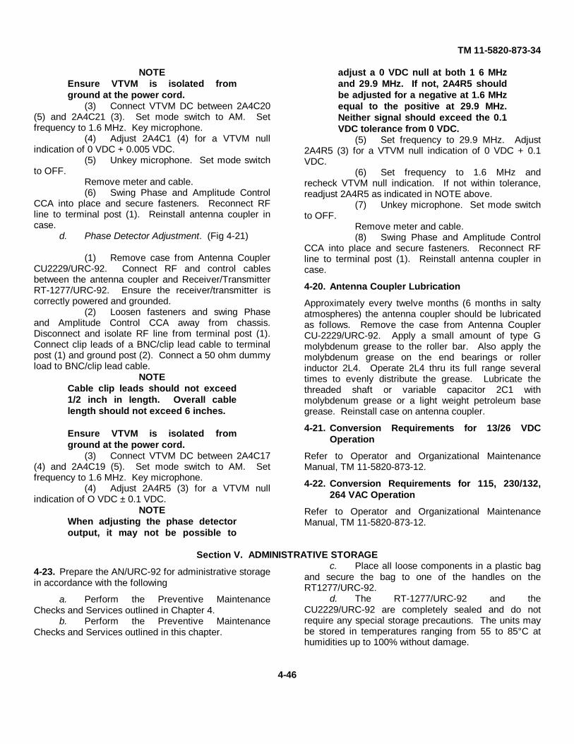
TM 11-5820-873-34
NOTEEnsure VTVM is isolated fromground at the power cord.
(3) Connect VTVM DC between 2A4C20(5) and 2A4C21 (3). Set mode switch to AM. Setfrequency to 1.6 MHz. Key microphone.
(4) Adjust 2A4C1 (4) for a VTVM nullindication of 0 VDC + 0.005 VDC.
(5) Unkey microphone. Set mode switchto OFF.
Remove meter and cable.(6) Swing Phase and Amplitude Control
CCA into place and secure fasteners. Reconnect RFline to terminal post (1). Reinstall antenna coupler incase.
d. Phase Detector Adjustment. (Fig 4-21)
(1) Remove case from Antenna CouplerCU2229/URC-92. Connect RF and control cablesbetween the antenna coupler and Receiver/TransmitterRT-1277/URC-92. Ensure the receiver/transmitter iscorrectly powered and grounded.
(2) Loosen fasteners and swing Phaseand Amplitude Control CCA away from chassis.Disconnect and isolate RF line from terminal post (1).Connect clip leads of a BNC/clip lead cable to terminalpost (1) and ground post (2). Connect a 50 ohm dummyload to BNC/clip lead cable.
NOTECable clip leads should not exceed1/2 inch in length. Overall cablelength should not exceed 6 inches.
Ensure VTVM is isolated fromground at the power cord.
(3) Connect VTVM DC between 2A4C17(4) and 2A4C19 (5). Set mode switch to AM. Setfrequency to 1.6 MHz. Key microphone.
(4) Adjust 2A4R5 (3) for a VTVM nullindication of O VDC ± 0.1 VDC.
NOTEWhen adjusting the phase detectoroutput, it may not be possible to
adjust a 0 VDC null at both 1 6 MHzand 29.9 MHz. If not, 2A4R5 shouldbe adjusted for a negative at 1.6 MHzequal to the positive at 29.9 MHz.Neither signal should exceed the 0.1VDC tolerance from 0 VDC.
(5) Set frequency to 29.9 MHz. Adjust2A4R5 (3) for a VTVM null indication of 0 VDC + 0.1VDC.
(6) Set frequency to 1.6 MHz andrecheck VTVM null indication. If not within tolerance,readjust 2A4R5 as indicated in NOTE above.
(7) Unkey microphone. Set mode switchto OFF.
Remove meter and cable.(8) Swing Phase and Amplitude Control
CCA into place and secure fasteners. Reconnect RFline to terminal post (1). Reinstall antenna coupler incase.
4-20. Antenna Coupler Lubrication
Approximately every twelve months (6 months in saltyatmospheres) the antenna coupler should be lubricatedas follows. Remove the case from Antenna CouplerCU-2229/URC-92. Apply a small amount of type Gmolybdenum grease to the roller bar. Also apply themolybdenum grease on the end bearings or rollerinductor 2L4. Operate 2L4 thru its full range severaltimes to evenly distribute the grease. Lubricate thethreaded shaft or variable capacitor 2C1 withmolybdenum grease or a light weight petroleum basegrease. Reinstall case on antenna coupler.
4-21. Conversion Requirements for 13/26 VDCOperation
Refer to Operator and Organizational MaintenanceManual, TM 11-5820-873-12.
4-22. Conversion Requirements for 115, 230/132,264 VAC Operation
Refer to Operator and Organizational MaintenanceManual, TM 11-5820-873-12.
Section V. ADMINISTRATIVE STORAGE
4-23. Prepare the AN/URC-92 for administrative storagein accordance with the following
a. Perform the Preventive MaintenanceChecks and Services outlined in Chapter 4.
b. Perform the Preventive MaintenanceChecks and Services outlined in this chapter.
c. Place all loose components in a plastic bagand secure the bag to one of the handles on theRT1277/URC-92.
d. The RT-1277/URC-92 and theCU2229/URC-92 are completely sealed and do notrequire any special storage precautions. The units maybe stored in temperatures ranging from 55 to 85°C athumidities up to 100% without damage.
4-46
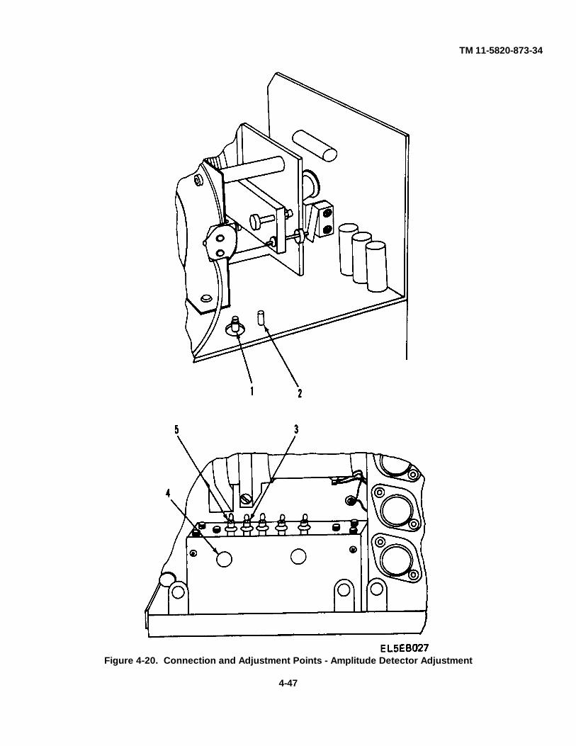
TM 11-5820-873-34
Figure 4-20. Connection and Adjustment Points - Amplitude Detector Adjustment
4-47
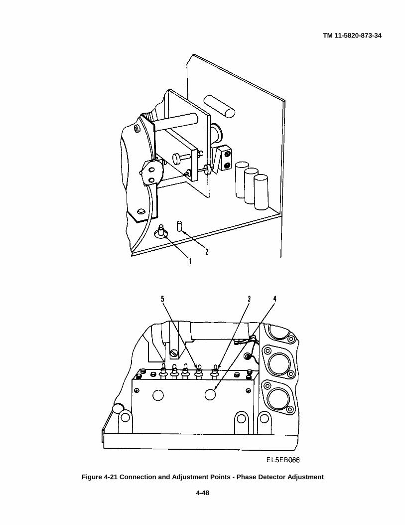
TM 11-5820-873-34
Figure 4-21 Connection and Adjustment Points - Phase Detector Adjustment
4-48
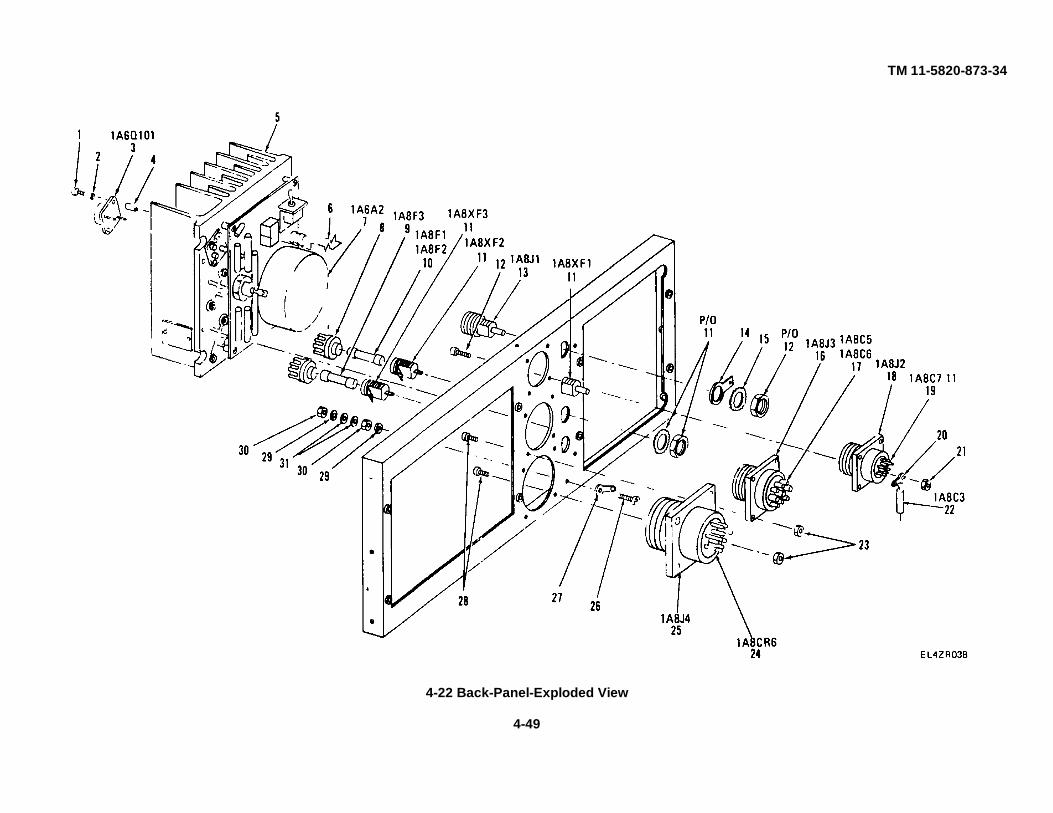
TM 11-5820-873-34
4-22 Back-Panel-Exploded View
4-49
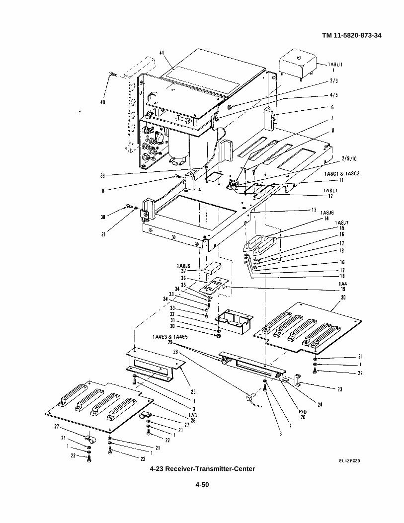
TM 11-5820-873-34
4-23 Receiver-Transmitter-Center
4-50
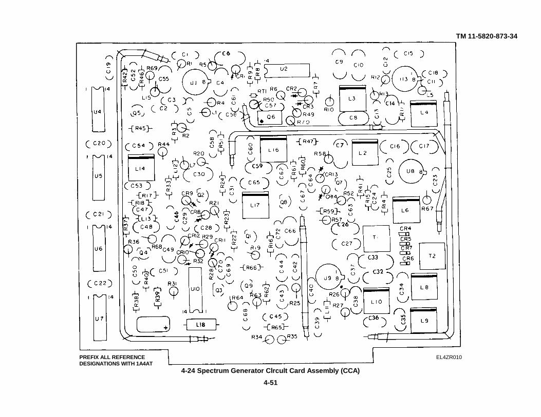
TM 11-5820-873-34
4-24 Spectrum Generator Clrcult Card Assembly (CCA)
PREFIX ALL REFERENCEDESIGNATIONS WITH 1A4AT
4-51
EL4ZR010
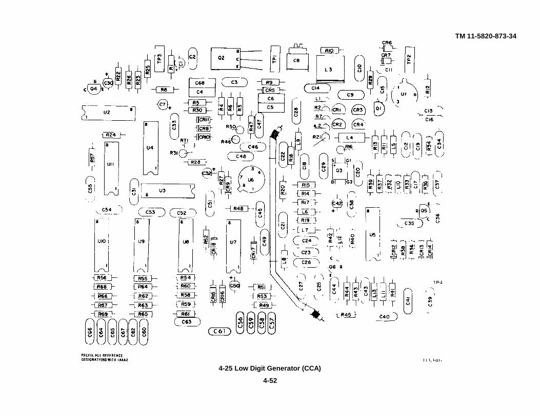
TM 11-5820-873-34
4-25 Low Digit Generator (CCA)
4-52
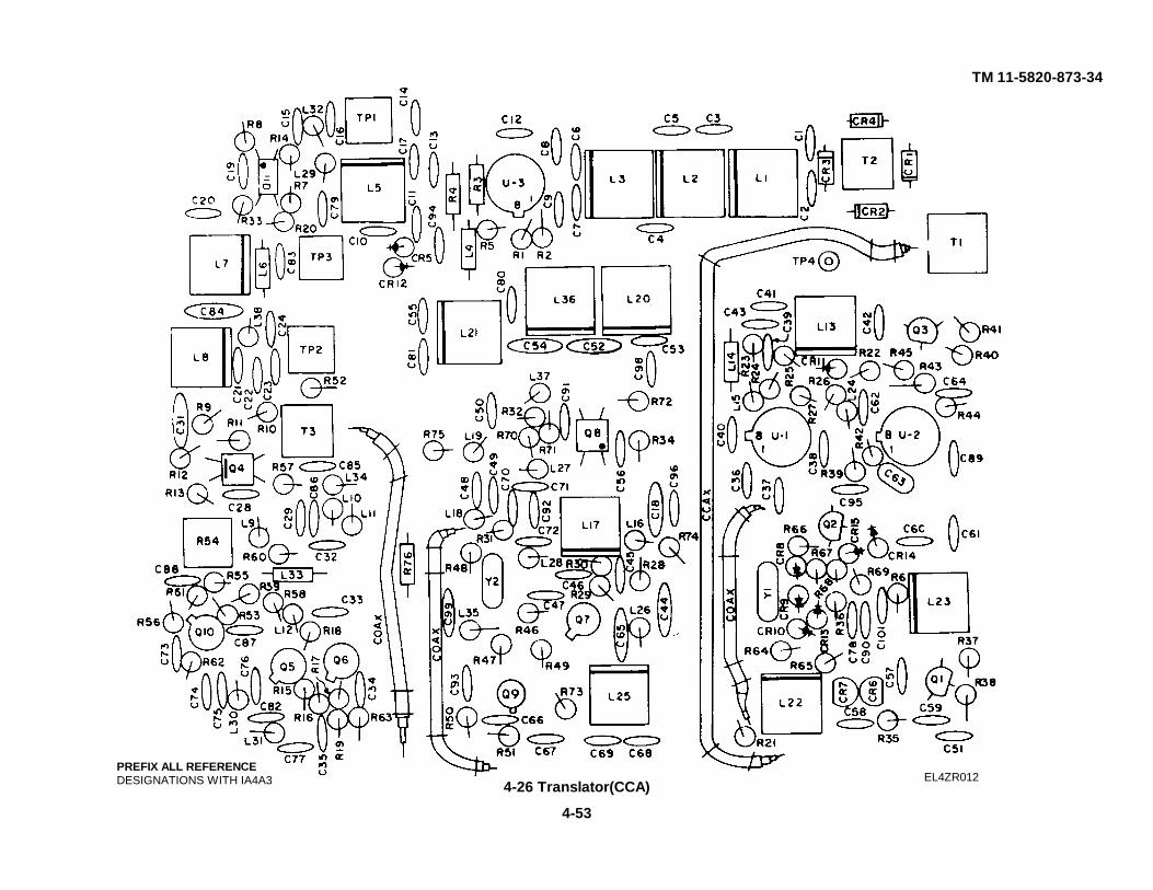
TM 11-5820-873-34
4-26 Translator(CCA)
4-53
PREFIX ALL REFERENCEDESIGNATIONS WITH IA4A3 EL4ZR012
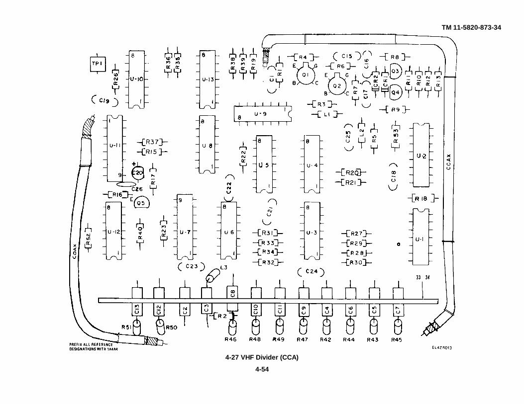
TM 11-5820-873-34
4-27 VHF Divider (CCA)
4-54
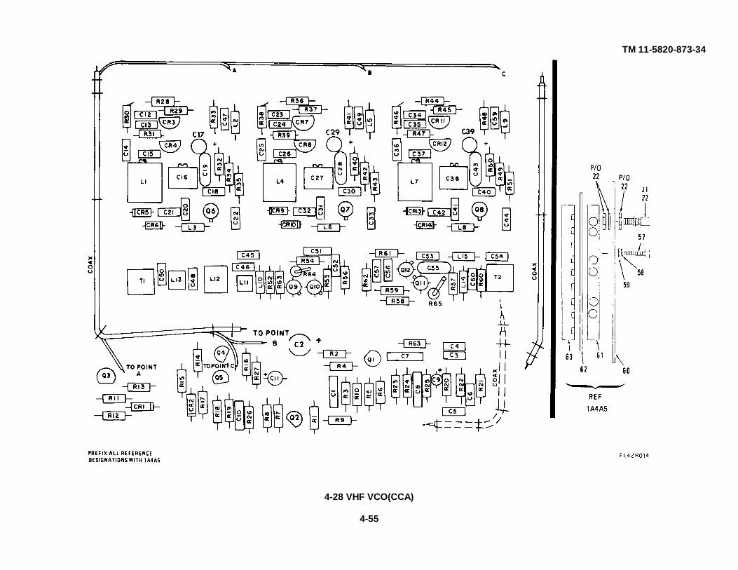
TM 11-5820-873-34
4-28 VHF VCO(CCA)
4-55
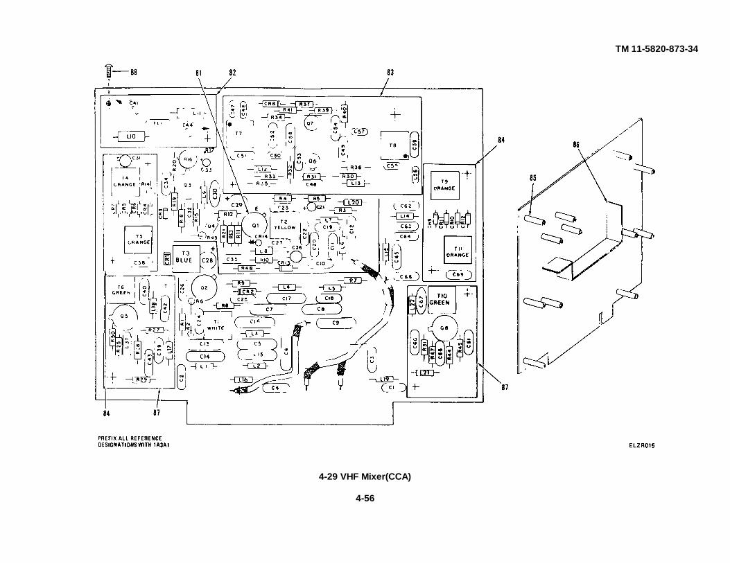
TM 11-5820-873-34
4-29 VHF Mixer(CCA)
4-56
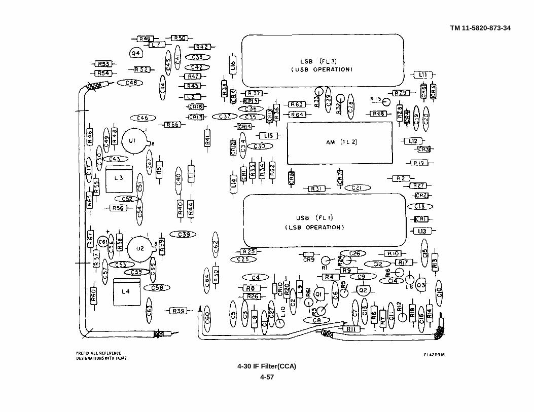
TM 11-5820-873-34
4-30 IF Filter(CCA)
4-57
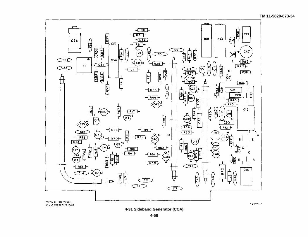
TM 11-5820-873-34
4-31 Sideband Generator (CCA)
4-58
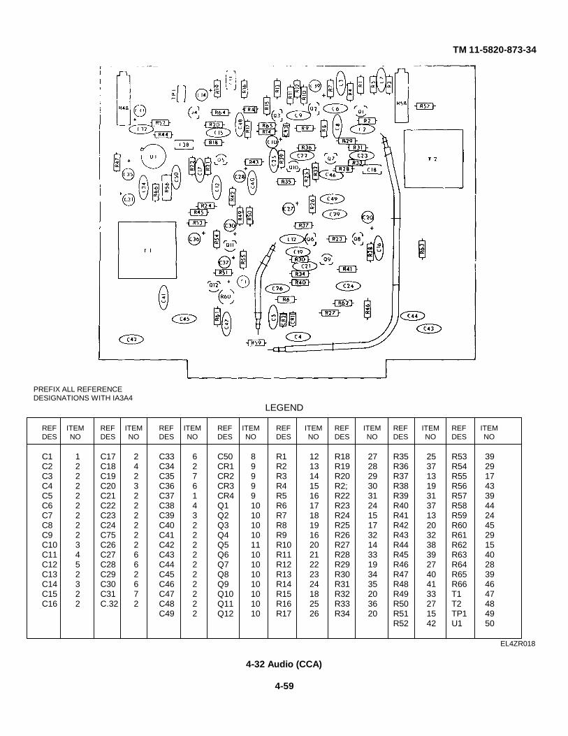
TM 11-5820-873-34
PREFIX ALL REFERENCEDESIGNATIONS WITH IA3A4
LEGEND
REF ITEM REF ITEM REF ITEM REF ITEM REF ITEM REF ITEM REF ITEM REF ITEMDES NO DES NO DES NO DES NO DES NO DES NO DES NO DES NO
C1 1 C17 2 C33 6 C50 8 R1 12 R18 27 R35 25 R53 39C2 2 C18 4 C34 2 CR1 9 R2 13 R19 28 R36 37 R54 29C3 2 C19 2 C35 7 CR2 9 R3 14 R20 29 R37 13 R55 17C4 2 C20 3 C36 6 CR3 9 R4 15 R2; 30 R38 19 R56 43C5 2 C21 2 C37 1 CR4 9 R5 16 R22 31 R39 31 R57 39C6 2 C22 2 C38 4 Q1 10 R6 17 R23 24 R40 37 R58 44C7 2 C23 2 C39 3 Q2 10 R7 18 R24 15 R41 13 R59 24C8 2 C24 2 C40 2 Q3 10 R8 19 R25 17 R42 20 R60 45C9 2 C75 2 C41 2 Q4 10 R9 16 R26 32 R43 32 R61 29C10 3 C26 2 C42 2 Q5 11 R10 20 R27 14 R44 38 R62 15C11 4 C27 6 C43 2 Q6 10 R11 21 R28 33 R45 39 R63 40C12 5 C28 6 C44 2 Q7 10 R12 22 R29 19 R46 27 R64 28C13 2 C29 2 C45 2 Q8 10 R13 23 R30 34 R47 40 R65 39C14 3 C30 6 C46 2 Q9 10 R14 24 R31 35 R48 41 R66 46C15 2 C31 7 C47 2 Q10 10 R15 18 R32 20 R49 33 T1 47C16 2 C.32 2 C48 2 Q11 10 R16 25 R33 36 R50 27 T2 48
C49 2 Q12 10 R17 26 R34 20 R51 15 TP1 49R52 42 U1 50
EL4ZR018
4-32 Audio (CCA)
4-59
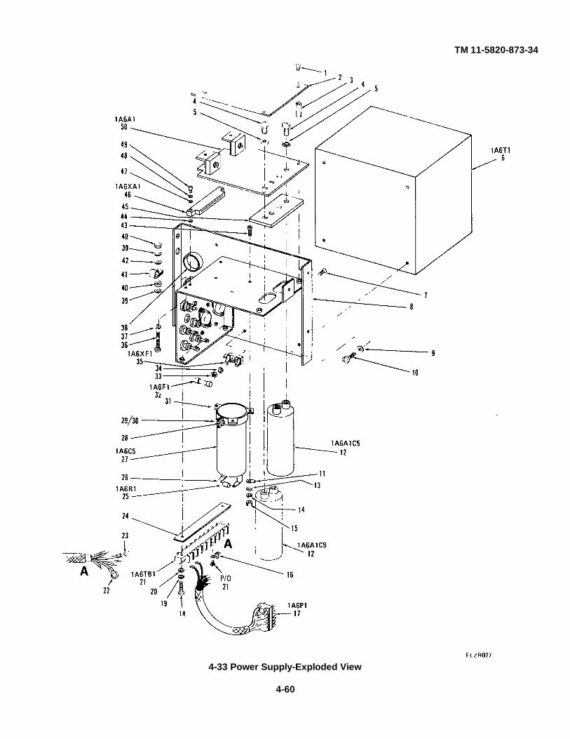
TM 11-5820-873-34
4-33 Power Supply-Exploded View
4-60
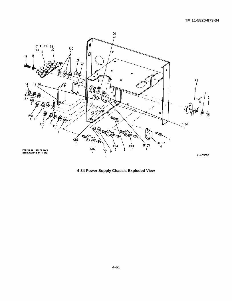
TM 11-5820-873-34
4-34 Power Supply Chassis-Exploded View
4-61
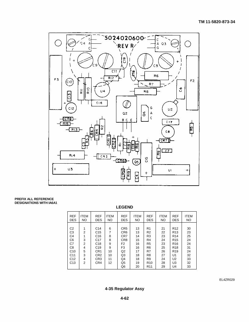
TM 11-5820-873-34
PREFIX ALL REFERENCEDESIGNATIONS WITH IA6A1
LEGEND
REF ITEM REF ITEM REF ITEM REF ITEM REF ITEMDES NO DES NO DES NO DES NO DES NO
C2 1 C14 6 CR5 13 R1 21 R12 30C3 2 C15 7 CR6 13 R2 22 R13 23C4 1 C16 8 CR7 14 R3 23 R14 25C6 3 C17 8 CR8 15 R4 24 R15 24C7 2 C18 9 F2 16 R5 23 R16 24C8 4 C19 9 F3 16 R6 25 R18 31C10 5 CR1 10 Q2 17 R7 26 R19 24C11 3 CR2 10 Q3 18 R8 27 U1 32C12 4 CR3 11 Q4 18 R9 24 U2 33C13 2 CR4 12 Q5 19 R10 28 U3 32
Q6 20 R11 29 U4 33
EL4ZR029
4-35 Regulator Assy
4-62
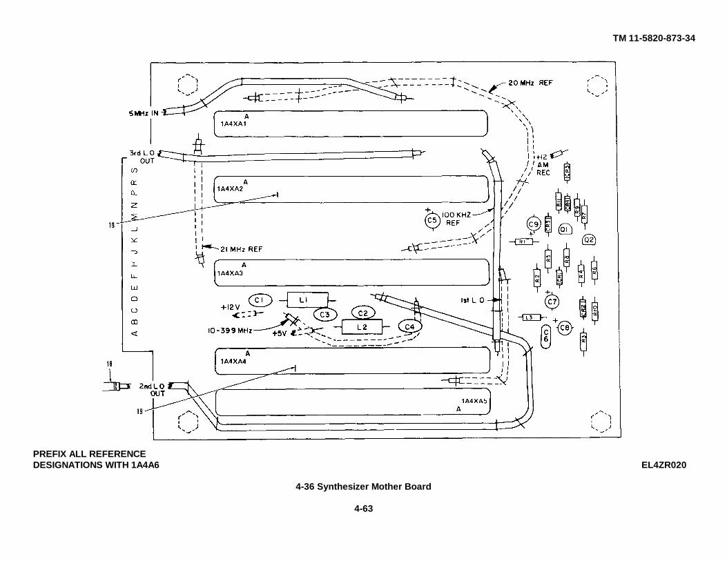
TM 11-5820-873-34
PREFIX ALL REFERENCEDESIGNATIONS WITH 1A4A6 EL4ZR020
4-36 Synthesizer Mother Board
4-63
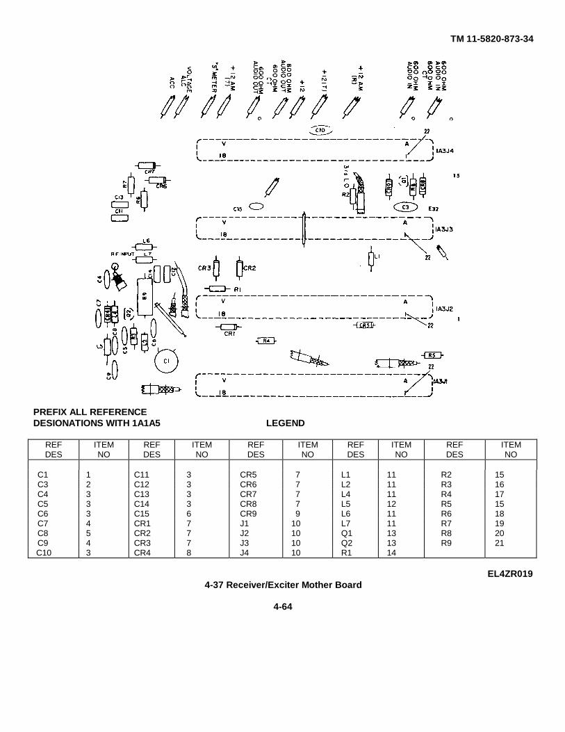
TM 11-5820-873-34
PREFIX ALL REFERENCEDESIONATIONS WITH 1A1A5 LEGEND
REFDES
ITEMNO
REFDES
ITEMNO
REFDES
ITEMNO
REFDES
ITEMNO
REFDES
ITEMNO
C1 1 C11 3 CR5 7 L1 11 R2 15C3 2 C12 3 CR6 7 L2 11 R3 16C4 3 C13 3 CR7 7 L4 11 R4 17C5 3 C14 3 CR8 7 L5 12 R5 15C6 3 C15 6 CR9 9 L6 11 R6 18C7 4 CR1 7 J1 10 L7 11 R7 19C8 5 CR2 7 J2 10 Q1 13 R8 20C9 4 CR3 7 J3 10 Q2 13 R9 21C10 3 CR4 8 J4 10 R1 14
EL4ZR0194-37 Receiver/Exciter Mother Board
4-64
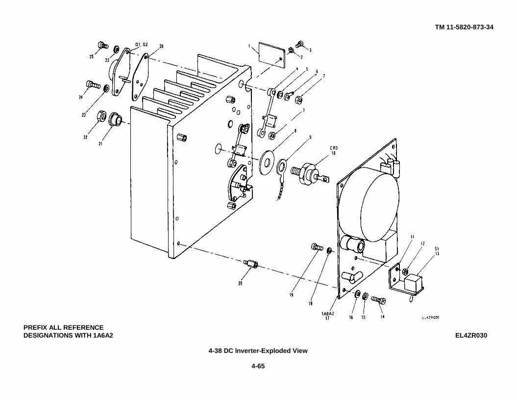
TM 11-5820-873-34
PREFIX ALL REFERENCEDESIGNATIONS WITH 1A6A2 EL4ZR030
4-38 DC lnverter-Exploded View
4-65
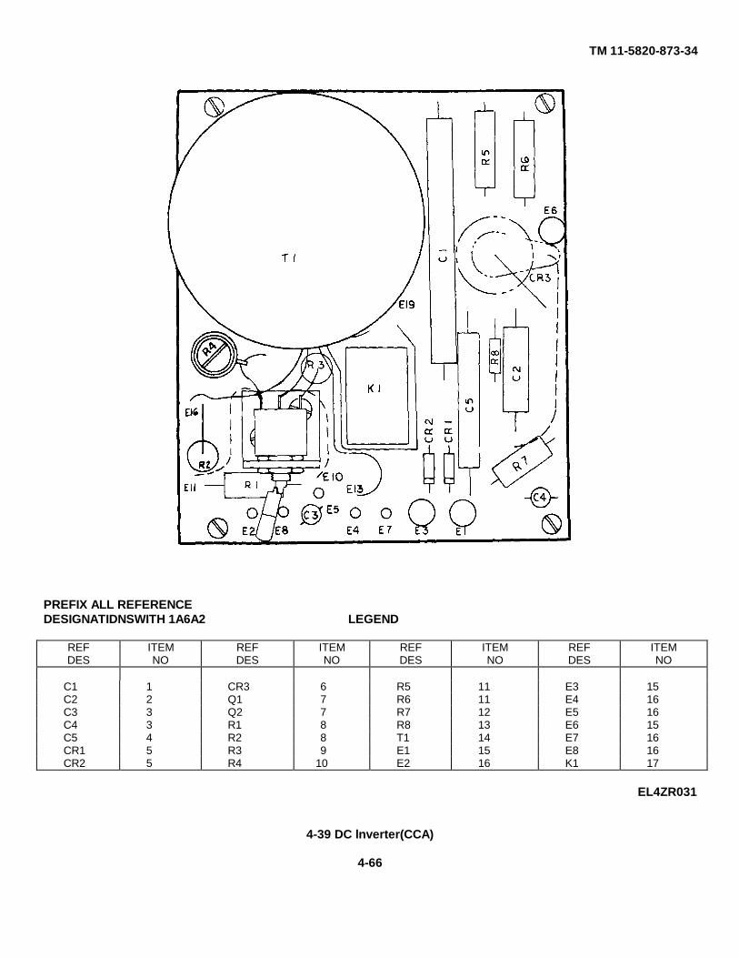
TM 11-5820-873-34
PREFIX ALL REFERENCEDESIGNATIDNSWITH 1A6A2 LEGEND
REFDES
ITEMNO
REFDES
ITEMNO
REFDES
ITEMNO
REFDES
ITEMNO
C1 1 CR3 6 R5 11 E3 15C2 2 Q1 7 R6 11 E4 16C3 3 Q2 7 R7 12 E5 16C4 3 R1 8 R8 13 E6 15C5 4 R2 8 T1 14 E7 16CR1 5 R3 9 E1 15 E8 16CR2 5 R4 10 E2 16 K1 17
EL4ZR031
4-39 DC lnverter(CCA)
4-66
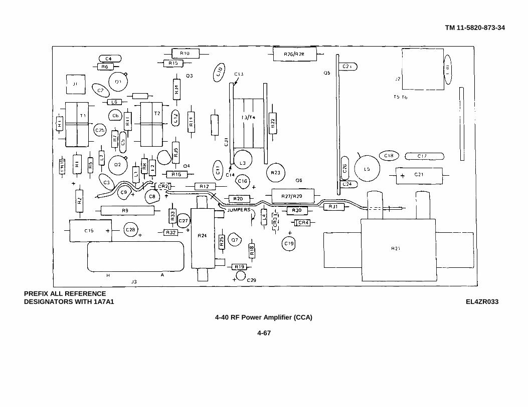
TM 11-5820-873-34
PREFIX ALL REFERENCEDESIGNATORS WITH 1A7A1 EL4ZR033
4-40 RF Power Amplifier (CCA)
4-67
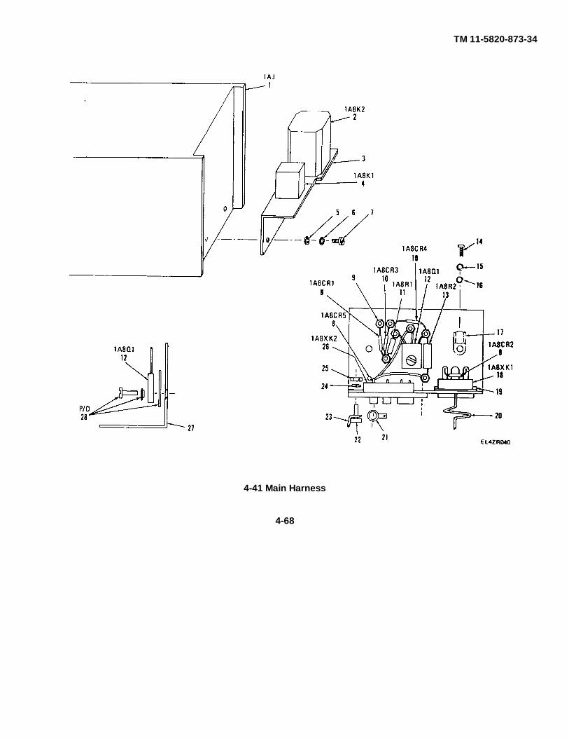
TM 11-5820-873-34
4-41 Main Harness
4-68
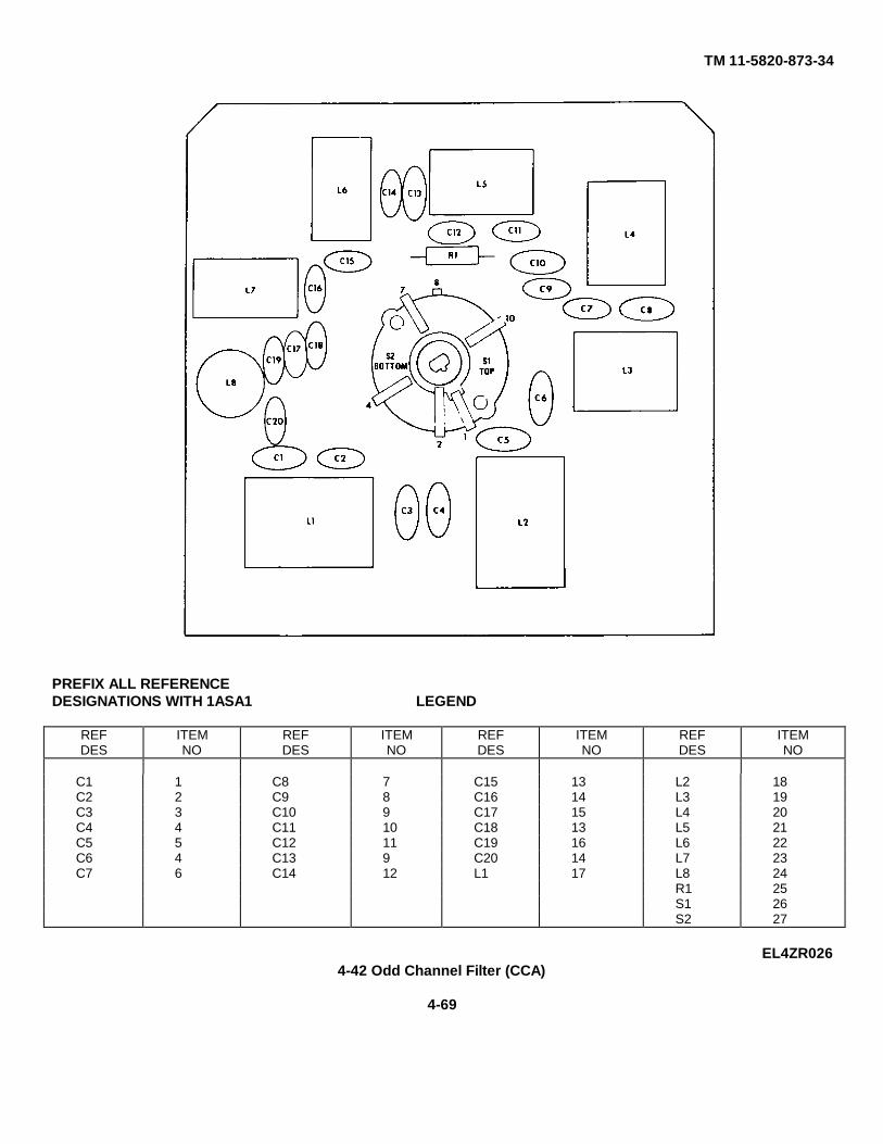
TM 11-5820-873-34
PREFIX ALL REFERENCEDESIGNATIONS WITH 1ASA1 LEGEND
REFDES
ITEMNO
REFDES
ITEMNO
REFDES
ITEMNO
REFDES
ITEMNO
C1 1 C8 7 C15 13 L2 18C2 2 C9 8 C16 14 L3 19C3 3 C10 9 C17 15 L4 20C4 4 C11 10 C18 13 L5 21C5 5 C12 11 C19 16 L6 22C6 4 C13 9 C20 14 L7 23C7 6 C14 12 L1 17 L8 24
R1 25S1 26S2 27
EL4ZR0264-42 Odd Channel Filter (CCA)
4-69
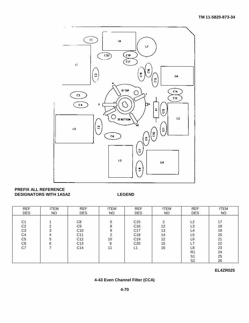
TM 11-5820-873-34
PREFIX ALL REFERENCEDESIGNATORS WITH 1ASA2 LEGEND
REFDES
ITEMNO
REFDES
ITEMNO
REFDES
ITEMNO
REFDES
ITEMNO
C1 1 C8 5 C15 2 L2 17C2 2 C9 8 C16 12 L3 18C3 3 C10 9 C17 13 L4 19C4 4 C11 2 C18 14 L5 20C5 5 C12 10 C19 12 L6 21C6 6 C13 9 C20 15 L7 22C7 7 C14 11 L1 16 L8 23
R1 24S1 25S2 26
EL4ZR025
4-43 Even Channel Filter (CCA)
4-70
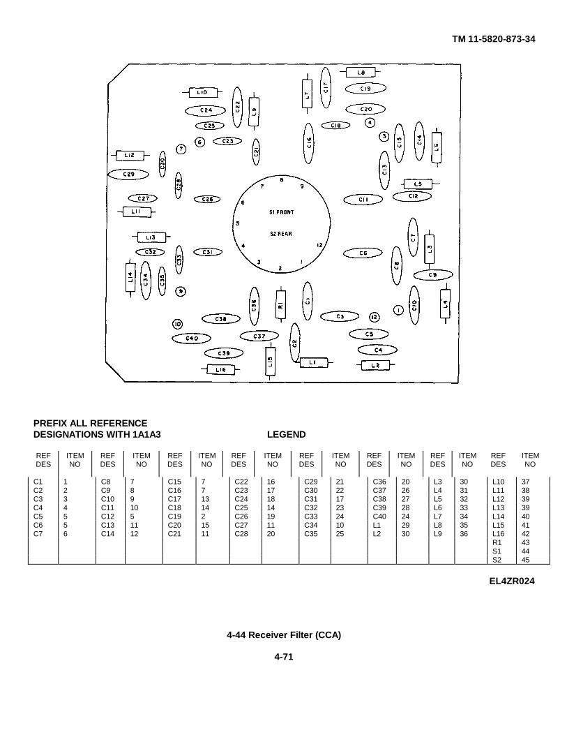
TM 11-5820-873-34
PREFIX ALL REFERENCEDESIGNATIONS WITH 1A1A3 LEGEND
REFDES
ITEMNO
REFDES
ITEMNO
REFDES
ITEMNO
REFDES
ITEMNO
REFDES
ITEMNO
REFDES
ITEMNO
REFDES
ITEMNO
REFDES
ITEMNO
C1 1 C8 7 C15 7 C22 16 C29 21 C36 20 L3 30 L10 37C2 2 C9 8 C16 7 C23 17 C30 22 C37 26 L4 31 L11 38C3 3 C10 9 C17 13 C24 18 C31 17 C38 27 L5 32 L12 39C4 4 C11 10 C18 14 C25 14 C32 23 C39 28 L6 33 L13 39C5 5 C12 5 C19 2 C26 19 C33 24 C40 24 L7 34 L14 40C6 5 C13 11 C20 15 C27 11 C34 10 L1 29 L8 35 L15 41C7 6 C14 12 C21 11 C28 20 C35 25 L2 30 L9 36 L16 42
R1 43S1 44S2 45
EL4ZR024
4-44 Receiver Filter (CCA)
4-71
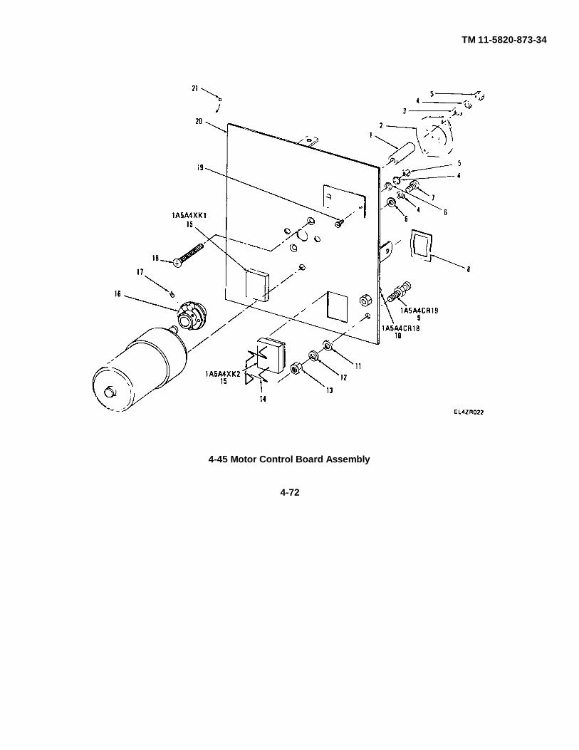
TM 11-5820-873-34
4-45 Motor Control Board Assembly
4-72
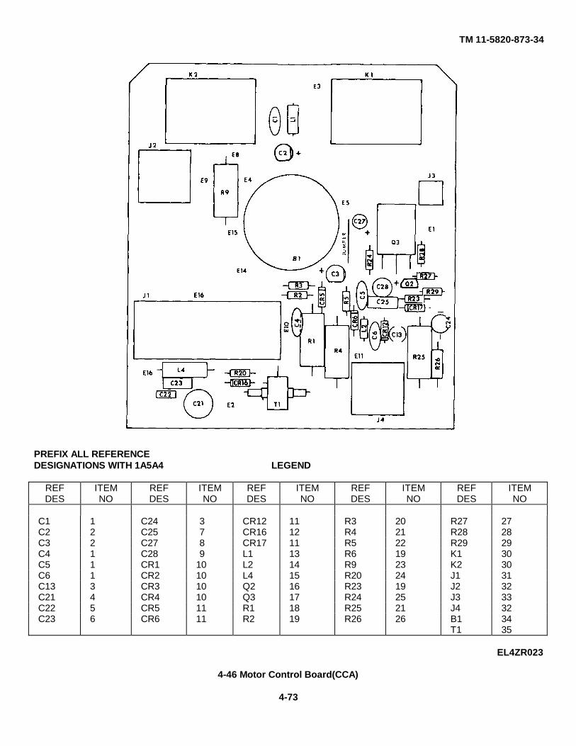
TM 11-5820-873-34
PREFIX ALL REFERENCEDESIGNATIONS WITH 1A5A4 LEGEND
REFDES
ITEMNO
REFDES
ITEMNO
REFDES
ITEMNO
REFDES
ITEMNO
REFDES
ITEMNO
C1 1 C24 3 CR12 11 R3 20 R27 27C2 2 C25 7 CR16 12 R4 21 R28 28C3 2 C27 8 CR17 11 R5 22 R29 29C4 1 C28 9 L1 13 R6 19 K1 30C5 1 CR1 10 L2 14 R9 23 K2 30C6 1 CR2 10 L4 15 R20 24 J1 31C13 3 CR3 10 Q2 16 R23 19 J2 32C21 4 CR4 10 Q3 17 R24 25 J3 33C22 5 CR5 11 R1 18 R25 21 J4 32C23 6 CR6 11 R2 19 R26 26 B1 34
T1 35
EL4ZR023
4-46 Motor Control Board(CCA)
4-73
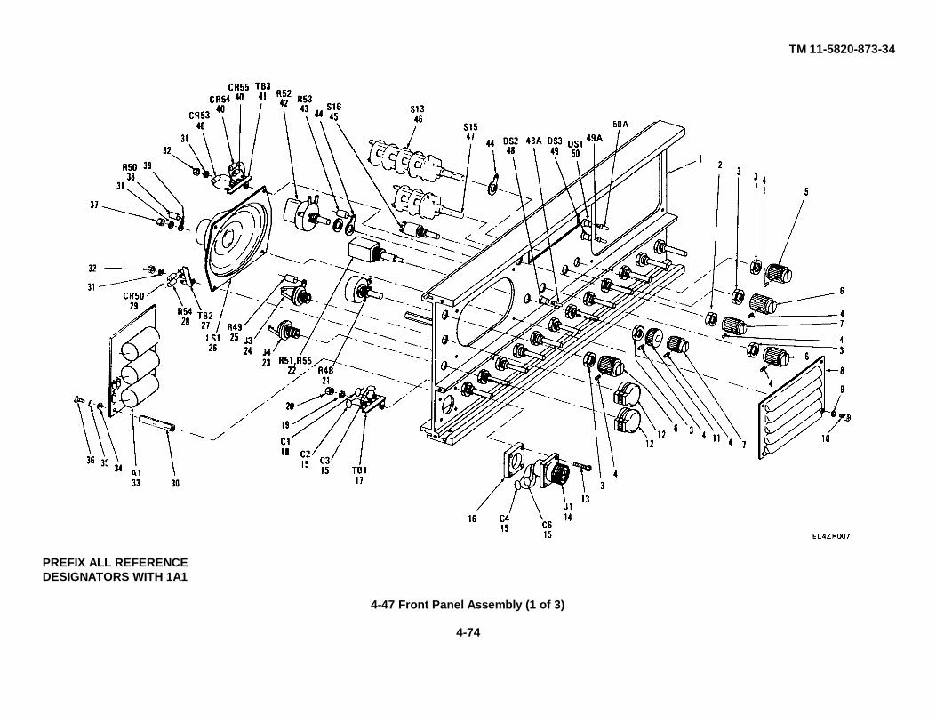
TM 11-5820-873-34
PREFIX ALL REFERENCEDESIGNATORS WITH 1A1
4-47 Front Panel Assembly (1 of 3)
4-74
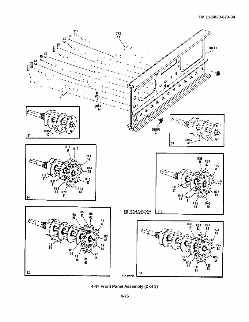
TM 11-5820-873-34
4-47 Front Panel Assembly (2 of 3)
4-75
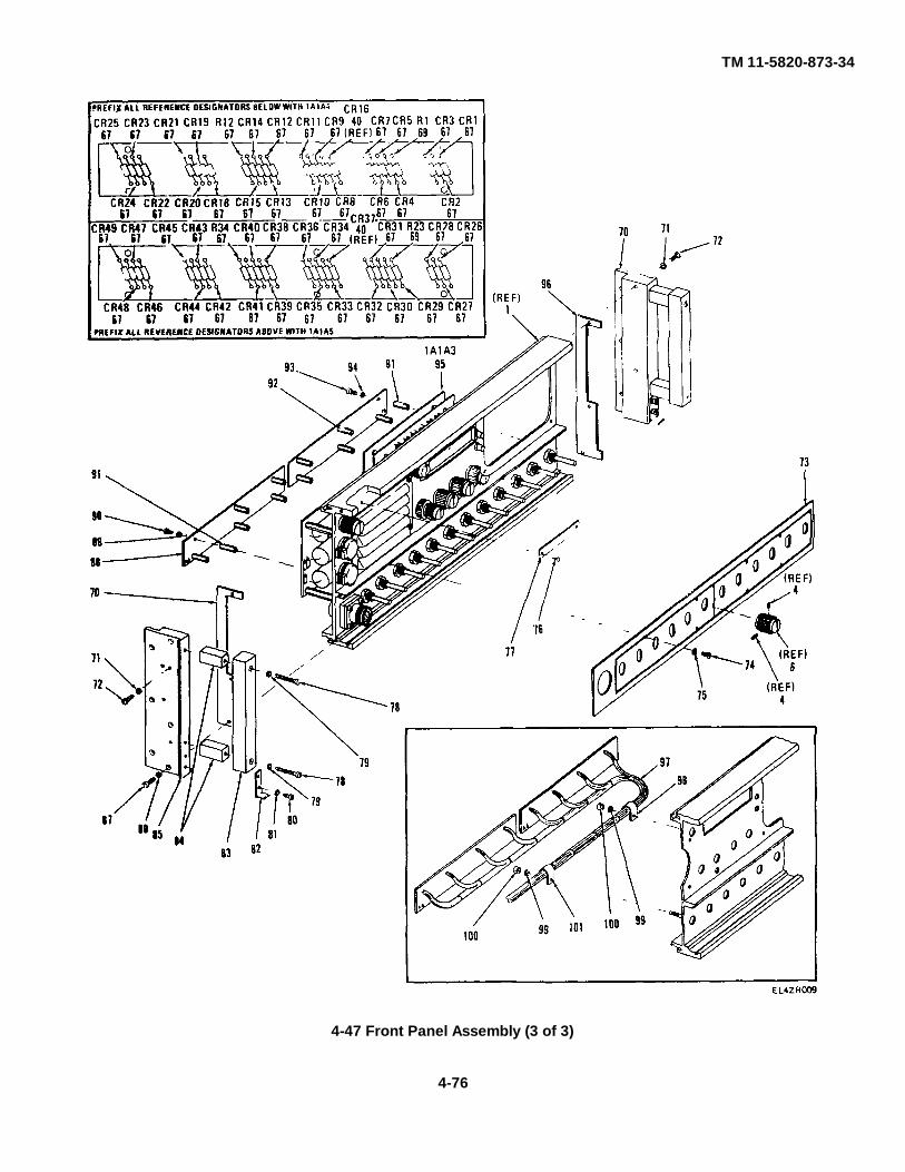
TM 11-5820-873-34
4-47 Front Panel Assembly (3 of 3)
4-76
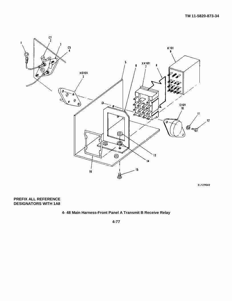
TM 11-5820-873-34
PREFIX ALL REFERENCEDESIGNATORS WITH 1A8
4- 48 Main Harness-Front Panel A Transmit B Receive Relay
4-77
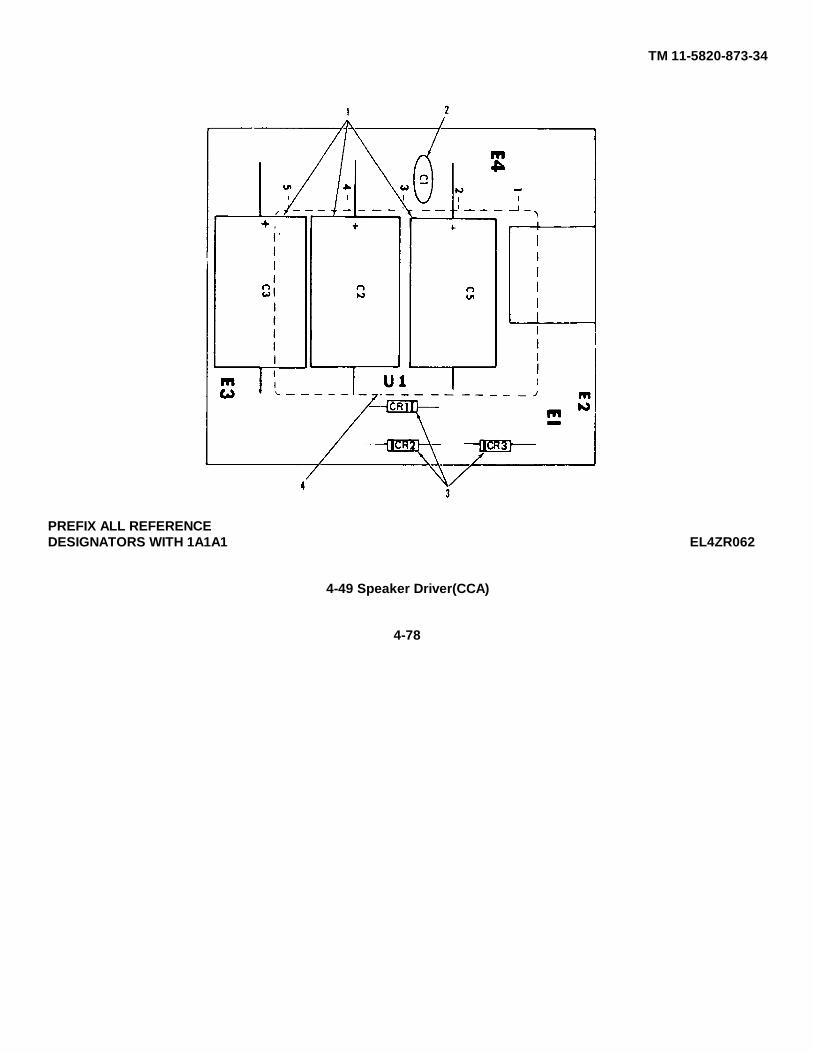
TM 11-5820-873-34
PREFIX ALL REFERENCEDESIGNATORS WITH 1A1A1 EL4ZR062
4-49 Speaker Driver(CCA)
4-78
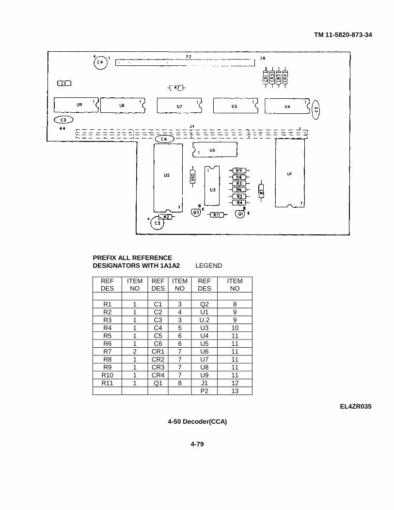
TM 11-5820-873-34
PREFIX ALL REFERENCEDESIGNATORS WITH 1A1A2 LEGEND
REF ITEM REF ITEM REF ITEMDES NO DES NO DES NO
R1 1 C1 3 Q2 8R2 1 C2 4 U1 9R3 1 C3 3 U.2 9R4 1 C4 5 U3 10R5 1 C5 6 U4 11R6 1 C6 6 U5 11R7 2 CR1 7 U6 11R8 1 CR2 7 U7 11R9 1 CR3 7 U8 11
R10 1 CR4 7 U9 11R11 1 Q1 8 J1 12
P2 13
EL4ZR035
4-50 Decoder(CCA)
4-79
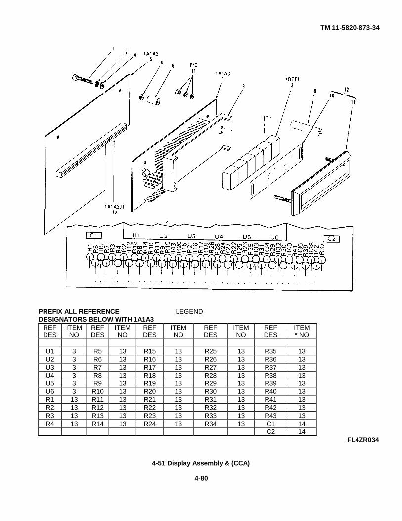
TM 11-5820-873-34
PREFIX ALL REFERENCE LEGENDDESIGNATORS BELOW WITH 1A1A3
REF ITEM REF ITEM REF ITEM REF ITEM REF ITEMDES NO DES NO DES NO DES NO DES * NO
U1 3 R5 13 R15 13 R25 13 R35 13U2 3 R6 13 R16 13 R26 13 R36 13U3 3 R7 13 R17 13 R27 13 R37 13U4 3 R8 13 R18 13 R28 13 R38 13U5 3 R9 13 R19 13 R29 13 R39 13U6 3 R10 13 R20 13 R30 13 R40 13R1 13 R11 13 R21 13 R31 13 R41 13R2 13 R12 13 R22 13 R32 13 R42 13R3 13 R13 13 R23 13 R33 13 R43 13R4 13 R14 13 R24 13 R34 13 C1 14
C2 14FL4ZR034
4-51 Display Assembly & (CCA)
4-80
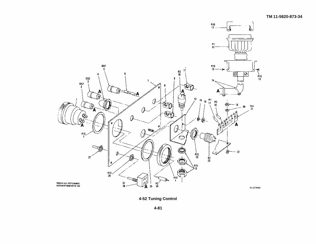
TM 11-5820-873-34
4-52 Tuning Control
4-81
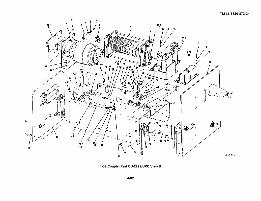
TM 11-5820-873-34
4-53 Coupler Unit CU-2229/URC View B
4-82
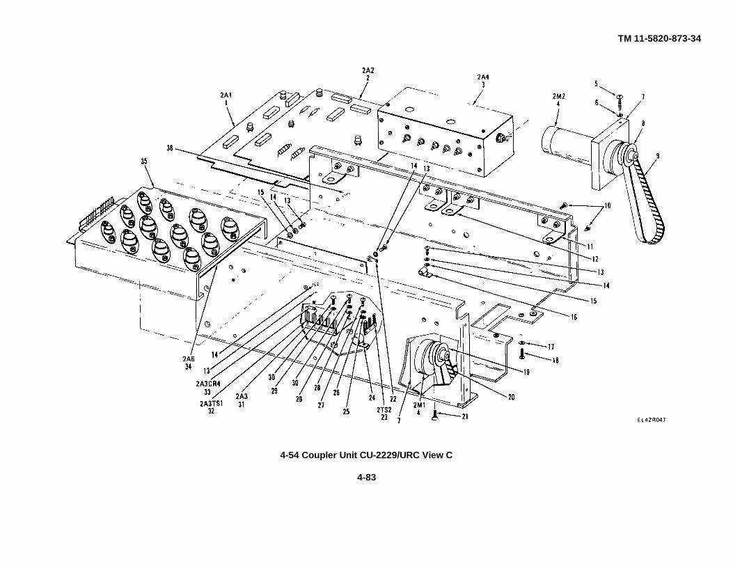
TM 11-5820-873-34
4-54 Coupler Unit CU-2229/URC View C
4-83
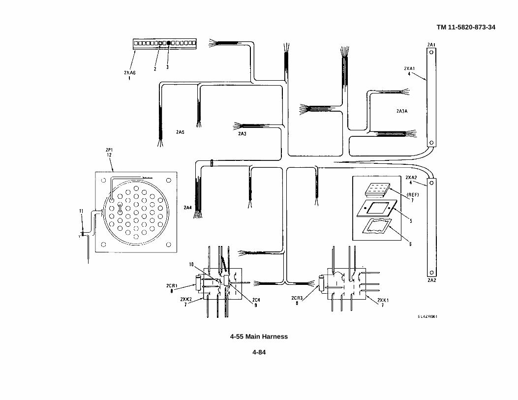
TM 11-5820-873-34
4-55 Main Harness
4-84
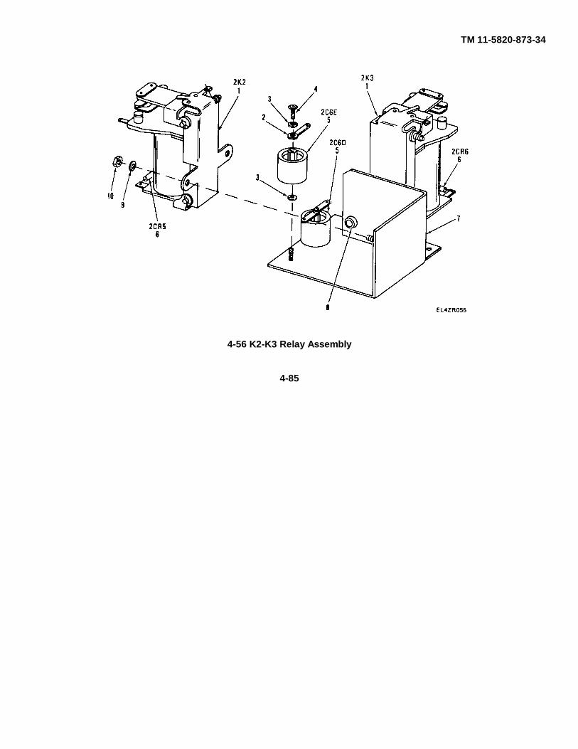
TM 11-5820-873-34
4-56 K2-K3 Relay Assembly
4-85
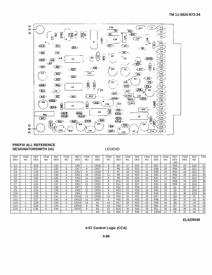
TM 11-5820-873-34
PREFIX ALL REFERENCEDESIGNATORSWITH 2A1 LEGEND
REF ITEM REF ITEM REF ITEM REF ITEM REF ITEM REF ITEM REF ITEM REF ITEM REF ITEM REF ITEMDES NO DES NO DES NO DES NO DES NO DES NO DES NO DES NO DES
, NODES NO
C1 1 C16 1 C31 7 C46 1 CR16 9 R5 17 R21 17 R37 17 R53 23 Q10 37C2 1 C17 1 C32 8 C47 4 CR17 9 R6 18 R22 17 R38 29 R54 35 Q11 37C3 1 C18 1 C33 8 CR1 9 CR18 9 R7 19 R23 19 R39 29 R55 19 Q12 37C4 1 C19 1 C34 8 CR2 10 CR19 11 R8 19 R24 28 R40 17 R56 28 Q13 39C5 1 C20 1 C35 3 CR3 11 CR20 9 R9 20 R25 16 R41 14 R57 17 Q14 37C6 1 C21 1 C36 8 CR4 11 CR21 9 R10 21 R26 17 R42 17 R58 19 Q15 38C7 1 C22 1 C37 2 CR5 11 CR22 9 R11 22 R27 17 R43 30 R59 19 Q16 37C8 1 C23 2 C38 3 CR7 9 CR23 9 R12 19 R28 17 R44 28 Q1 36 Q17 40C9 1 C24 1 C39 8 CR8 12 CR24 9 R13 23 R29 19 R45 19 Q2 37 Q18 38C10 1 C25 3 C40 8 CR9 9 CR25 9 R14 23 R30 29 R46 31 Q3 38 Q19 39C11 1 C26 3 C41 1 CR10 11 CR26 12 R15 24 R31 19 R47 32 Q4 37 U1 41C12 I C27 4 C42 8 CR12 11 CR27 9 R16 25 R32 29 R48 33 Q5 37 U2 42C13 1 C28 2 C43 3 CR13 13 R1 14 R17 25 R33 29 R49 34 Q6 37 U3 42C14 1 C29 5 C44 1 CR14 9 R2 14 R18 17 R34 29 R50 25 Q7 37 U4 42C15 1 C30 6 C45 1 CR15 9 R3 15 R19 26 R35 29 R51 26 Q8 39 U5 42
R4 16 R20 27 R36 29 CR52 27 09 37 U6 42
EL4ZR048
4-57 Control Logic (CCA)
4-86
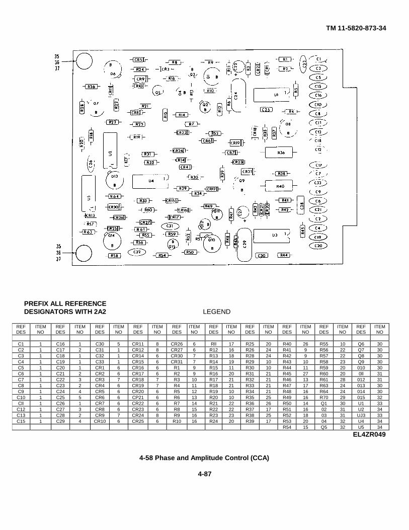
TM 11-5820-873-34
PREFIX ALL REFERENCEDESIGNATORS WITH 2A2 LEGEND
REF ITEM REF ITEM REF ITEM REF ITEM REF ITEM REF ITEM REF ITEM REF ITEM REF ITEM REF ITEMDES NO DES NO DES NO DES NO DES NO DES NO DES NO DES NO DES NO DES NO
C1 1 C16 1 C30 5 CR11 8 CR26 6 Rll 17 R25 20 R40 26 R55 10 Q6 30C2 1 C17 2 C31 1 CR12 8 CR27 6 R12 16 R26 24 R41 9 R56 22 Q7 30C3 1 C18 1 C32 1 CR14 6 CR30 7 R13 18 R28 24 R42 9 R57 22 Q8 30C4 1 C19 1 C33 1 CR15 6 CR31 7 R14 19 R29 10 R43 10 R58 23 Q9 30C5 1 C20 1 CR1 6 CR16 6 R1 9 R15 11 R30 10 R44 11 R59 20 010 30C6 1 C21 2 CR2 6 CR17 6 R2 9 R16 20 R31 21 R45 27 R60 20 0ll 31C7 1 C22 3 CR3 7 CR18 7 R3 10 R17 21 R32 21 R46 13 R61 28 012 31C8 1 C23 2 CR4 6 CR19 7 R4 11 R18 21 R33 21 R47 17 R63 24 013 30C9 1 C24 4 CR5 6 CR20 6 R5 12 R19 10 R34 21 R48 16 R64 24 014 30C10 1 C25 5 CR6 6 CP21 6 R6 13 R20 10 R35 25 R49 16 R70 29 015 32Cll 1 C26 1 CR7 6 CR22 6 R7 14 R21 22 R36 26 R50 14 Q1 30 U1 33
C12 1 C27 3 CR8 6 CR23 6 R8 15 R22 22 R37 17 R51 16 02 31 U2 34C13 1 C28 2 CR9 7 CR24 8 R9 16 R23 23 R38 25 R52 18 03 31 UJ3 33C15 1 C29 4 CR10 6 CR25 6 R10 16 R24 20 R39 17 R53 20 04 32 U4 34
R54 15 Q5 32 U5 34
EL4ZR049
4-58 Phase and Amplitude Control (CCA)
4-87
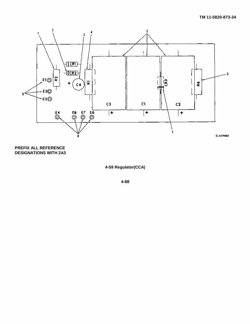
TM 11-5820-873-34
PREFIX ALL REFERENCEDESIGNATIONS WITH 2A3
4-59 Regulator(CCA)
4-88
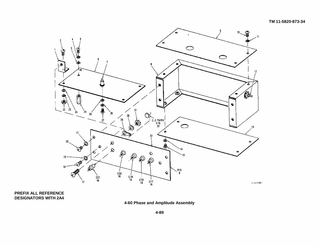
TM 11-5820-873-34
PREFIX ALL REFERENCEDESIGNATORS WITH 2A4
4-60 Phase and Amplitude Assembly
4-89
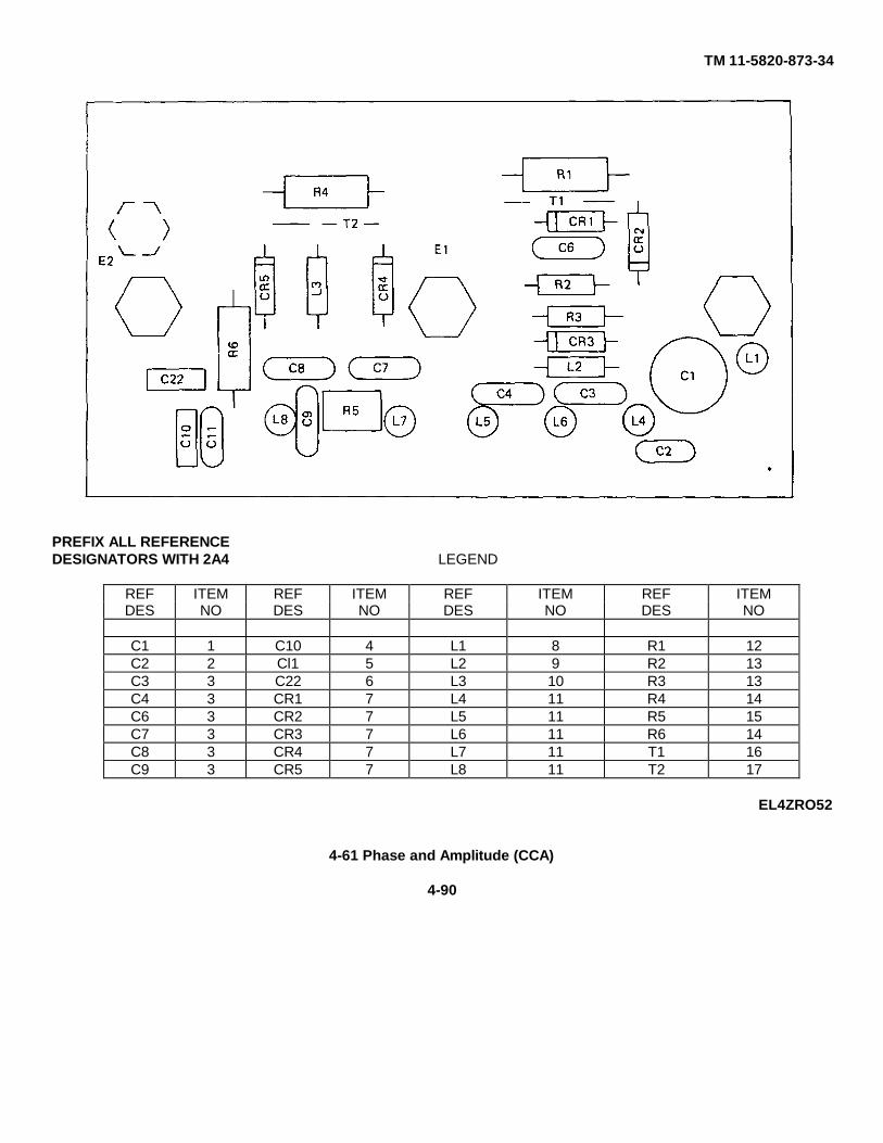
TM 11-5820-873-34
PREFIX ALL REFERENCEDESIGNATORS WITH 2A4 LEGEND
REF ITEM REF ITEM REF ITEM REF ITEMDES NO DES NO DES NO DES NO
C1 1 C10 4 L1 8 R1 12C2 2 Cl1 5 L2 9 R2 13C3 3 C22 6 L3 10 R3 13C4 3 CR1 7 L4 11 R4 14C6 3 CR2 7 L5 11 R5 15C7 3 CR3 7 L6 11 R6 14C8 3 CR4 7 L7 11 T1 16C9 3 CR5 7 L8 11 T2 17
EL4ZRO52
4-61 Phase and Amplitude (CCA)
4-90
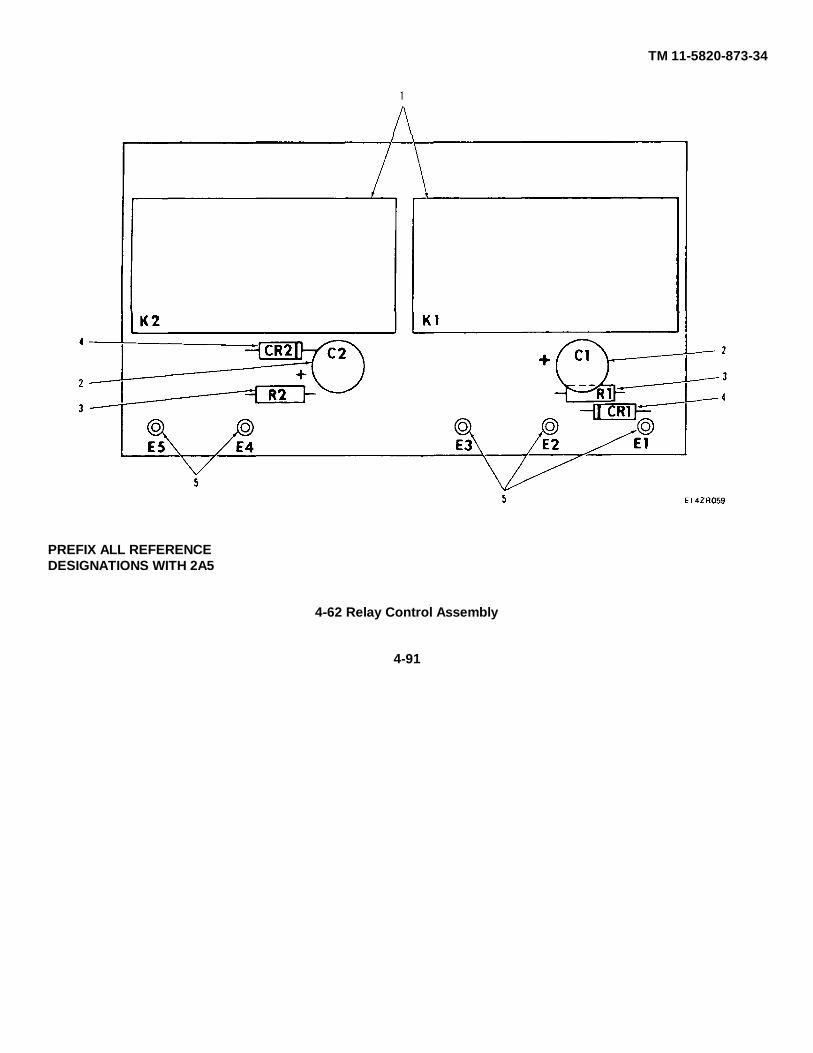
TM 11-5820-873-34
PREFIX ALL REFERENCEDESIGNATIONS WITH 2A5
4-62 Relay Control Assembly
4-91
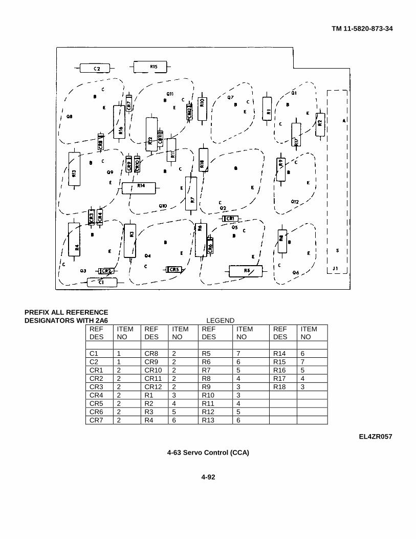
TM 11-5820-873-34
PREFIX ALL REFERENCEDESIGNATORS WITH 2A6 LEGEND
REF ITEM REF ITEM REF ITEM REF ITEMDES NO DES NO DES NO DES NO
C1 1 CR8 2 R5 7 R14 6C2 1 CR9 2 R6 6 R15 7CR1 2 CR10 2 R7 5 R16 5CR2 2 CR11 2 R8 4 R17 4CR3 2 CR12 2 R9 3 R18 3CR4 2 R1 3 R10 3CR5 2 R2 4 R11 4CR6 2 R3 5 R12 5CR7 2 R4 6 R13 6
EL4ZR057
4-63 Servo Control (CCA)
4-92
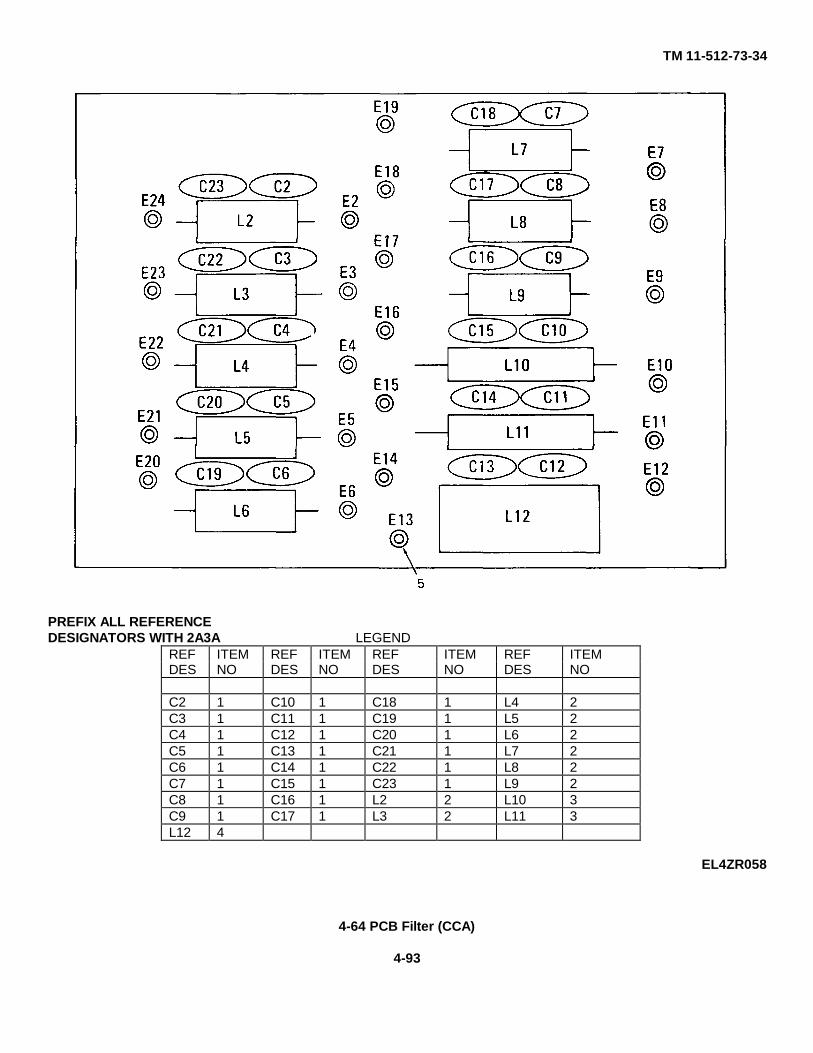
TM 11-512-73-34
PREFIX ALL REFERENCEDESIGNATORS WITH 2A3A LEGEND
REF ITEM REF ITEM REF ITEM REF ITEMDES NO DES NO DES NO DES NO
C2 1 C10 1 C18 1 L4 2C3 1 C11 1 C19 1 L5 2C4 1 C12 1 C20 1 L6 2C5 1 C13 1 C21 1 L7 2C6 1 C14 1 C22 1 L8 2C7 1 C15 1 C23 1 L9 2C8 1 C16 1 L2 2 L10 3C9 1 C17 1 L3 2 L11 3L12 4
EL4ZR058
4-64 PCB Filter (CCA)
4-93
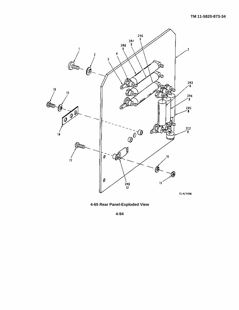
TM 11-5820-873-34
4-65 Rear Panel-Exploded View
4-94
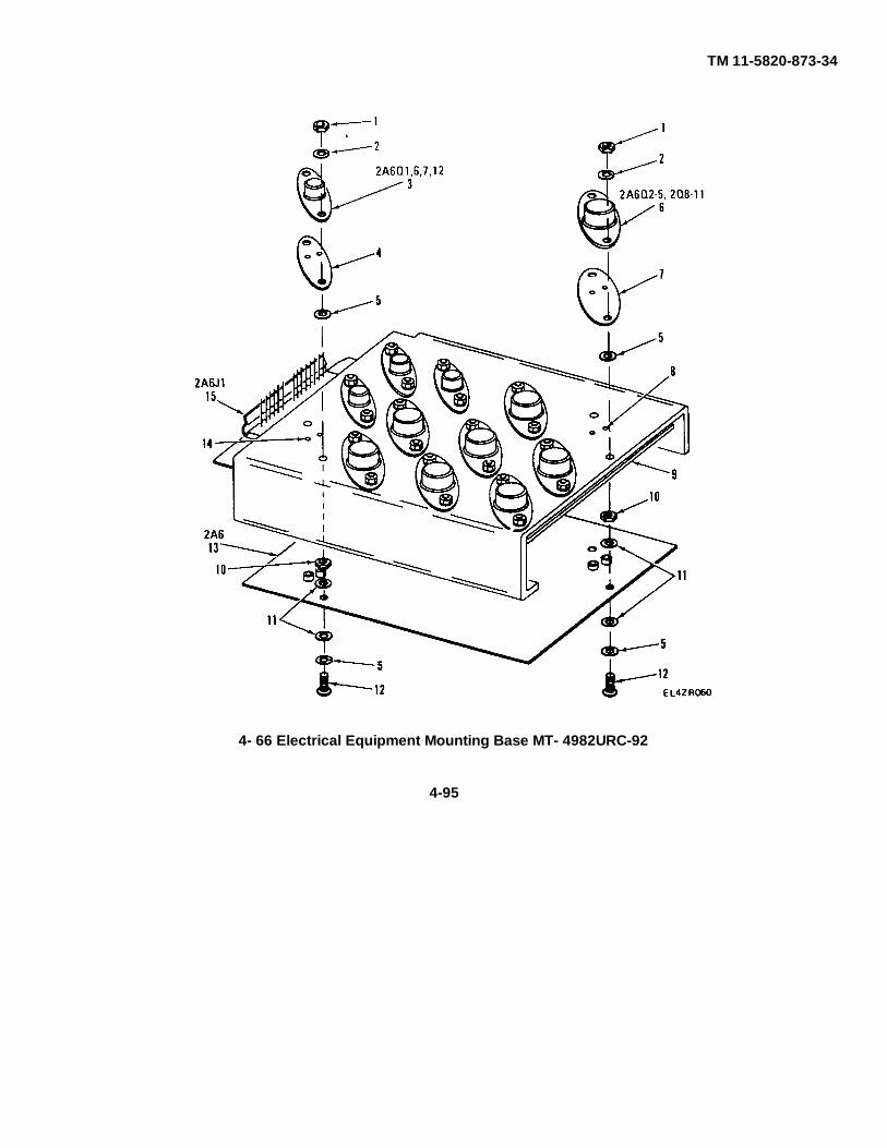
TM 11-5820-873-34
4- 66 Electrical Equipment Mounting Base MT- 4982URC-92
4-95
TM 11-5820-873-34
APPENDIX A
REFERENCES
DA Pam 310-4 Index of Technical Manuals, Technical Bulletins, Supply Manuals (Types 7, 8, and 9),Supply Bulletins, and Lubrication Orders.
DA Pam 310-7 US Army Equipment Index of Modification Work Orders.SB 700-20 Army Adopted/Other Items Selected for Authorization/List of Reportable Items.TB SIG 291 Safety Measures to Be Observed When Installing and Using Whip Antennas, Field
Type Masts, Towers, Antennas, and Metal Poles That Are Used with Communication,Radar, and Direction Finder Equipment.
TB 43-0118 Field Instructions for Painting and Preserving Electronics Command Equipment IncludingCamouflage Pattern Painting of Electrical Equipment Shelters
TB 38-750 The Army Maintenance Management System.TM 750-244-2 Procedures for Destruction of Electronics Materiel to Prevent Enemy Use (Electronics
Command).
A-1
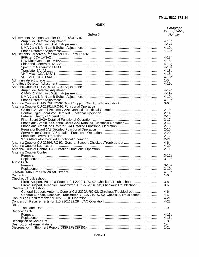
TM 11-5820-873-34
INDEXParagraph
Figure, Table,Subject Number
Adjustments, Antenna Coupler CU-2229/URC-92Amplitude Detector Adjustment ................................................................................................ 4-19cC MAXIC MIN Limit Switch Adjustment .................................................................................... 4-19aL MAX and L MIN Limit Switch Adjustment .............................................................................. 4-19bPhase Detector Adjustment...................................................................................................... 4-19d
Adjustments, Receiver-Transmitter RT-1277/URC-92IF/Filter CCA 1A3A2 ................................................................................................................ 4-18fLow Digit Generator 1A4A2...................................................................................................... 4-18bSideband Generator 1A3A3...................................................................................................... 4-18gSpectrum Generator 1A4A1 ..................................................................................................... 4-18aTranslator 1A4A3 ..................................................................................................................... 4-18cVHF Mixer CCA 1A3A1............................................................................................................ 4-18eVHF VCO CCA 1A4A5............................................................................................................. 4-18d
Administrative Storage....................................................................................................................... 1-5Amplitude Detector Adjustment .......................................................................................................... 4-19cAntenna Coupler CU-22291URC-92 Adjustments
Amplitude Detector Adjustment ................................................................................................ 4-19cC MAXIC MIN Limit Switch Adjustment .................................................................................... 4-19aL MAX and L MIN Limit Switch Adjustment. ............................................................................. 4-19bPhase Detector Adjustment...................................................................................................... 4-19d
Antenna Coupler CU-2229/URC-92 Direct Support Checkout/Troubleshoot........................................ 3-6Antenna Coupler CU-22291URC-92 Functional Operation
C3 and C6 Control Assembly 2A5 Detailed Functional Operation............................................. 2-19Control Logic Board 2A1 Detailed Functional Operation ........................................................... 2-14Detailed Theory of Operation ................................................................................................... 2-13Filter Board 2A3A Detailed Functional Operation .................................................................... 2-17Phase and Amplitude Control Board 2A2 Detailed Functional Operation .................................. 2-15Phase and Amplitude Detector 2A4 Detailed Functional Operation .......................................... 2-18Regulator Board 2A3 Detailed Functional Operation ................................................................ 2-16Servo Motor Control 2A6 Detailed Functional Operation .......................................................... 2-20Simplified Overall Operation .................................................................................................... 2-123 dB Attenuator Detailed Functional Operation......................................................................... 2-21
Antenna Coupler CU-2229/URC-92, General Support Checkout/Troubleshoot ................................... 4-6Antenna Coupler Lubrication ............................................................................................................. 4-20Antenna Coupler Control 1 A2 Detailed Functional Operation ............................................................ 2-11Antenna Coupler Control
Removal .................................................................................................................................. 3-12aReplacement............................................................................................................................ 3-12b
Audio CCARemoval .................................................................................................................................. 3-10aReplacement ........................................................................................................................... 3-10b
C MAXIC MIN Limit Switch Adjustment ............................................................................................. 4-19aCalibration ......................................................................................................................................... 1-6Checkout/Troubleshoot
Direct Support, Antenna Coupler CU-22291URC-92, Checkout/Troubleshoot .......................... 3-8Direct Support, Receiver-Transmitter RT-1277/URC-92, Checkout/Troubleshoot .................... 3-5
Checkout/TroubleshootGeneral Support, Antenna Coupler CU-2229/URC-92, Checkout/Troubleshoot ....................... 4-6General Support, Receiver-Transmitter RT-12771URC-92, Checkout/Troubleshoot ................. 4-5
Conversion Requirements for 13/26 VDC Operation ......................................................................... 4-21Conversion Requirements for 115,2301132,284 VAC Operation ........................................................ 4-22Data
Tabulated Data ........................................................................................................................ 1-9Decoder CCA
Removal .................................................................................................................................. 4-16aReplacement............................................................................................................................ 4-16b
Description of Radio Set .................................................................................................................... 1-8Destruction of Army Materiel ............................................................................................................. 1-4Discrepancy in Shipment Report (DISREP) (SF361) .......................................................................... 1-2c
Index 1
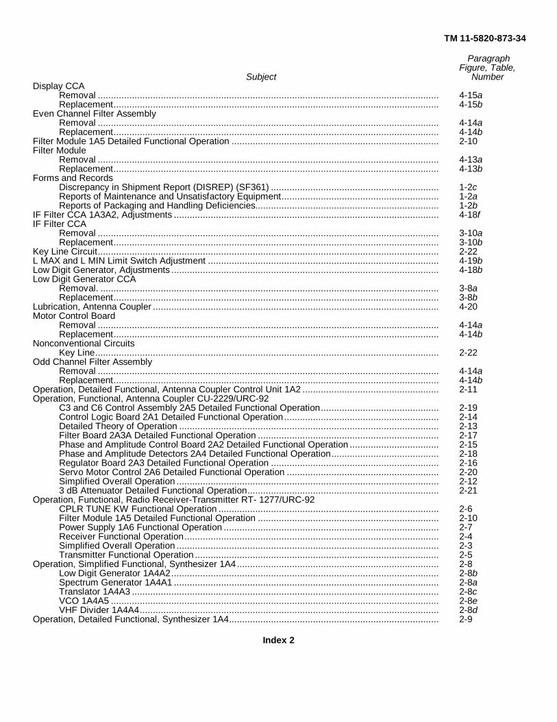
TM 11-5820-873-34
ParagraphFigure, Table,
Subject NumberDisplay CCA
Removal .................................................................................................................................. 4-15aReplacement............................................................................................................................ 4-15b
Even Channel Filter AssemblyRemoval .................................................................................................................................. 4-14aReplacement............................................................................................................................ 4-14b
Filter Module 1A5 Detailed Functional Operation ............................................................................... 2-10Filter Module
Removal .................................................................................................................................. 4-13aReplacement............................................................................................................................ 4-13b
Forms and RecordsDiscrepancy in Shipment Report (DISREP) (SF361) ................................................................ 1-2cReports of Maintenance and Unsatisfactory Equipment............................................................ 1-2aReports of Packaging and Handling Deficiencies...................................................................... 1-2b
IF Filter CCA 1A3A2, Adjustments ..................................................................................................... 4-18fIF Filter CCA
Removal .................................................................................................................................. 3-10aReplacement............................................................................................................................ 3-10b
Key Line Circuit.................................................................................................................................. 2-22L MAX and L MIN Limit Switch Adjustment ........................................................................................ 4-19bLow Digit Generator, Adjustments ...................................................................................................... 4-18bLow Digit Generator CCA
Removal. ................................................................................................................................. 3-8aReplacement............................................................................................................................ 3-8b
Lubrication, Antenna Coupler ............................................................................................................. 4-20Motor Control Board
Removal .................................................................................................................................. 4-14aReplacement............................................................................................................................ 4-14b
Nonconventional CircuitsKey Line................................................................................................................................... 2-22
Odd Channel Filter AssemblyRemoval .................................................................................................................................. 4-14aReplacement............................................................................................................................ 4-14b
Operation, Detailed Functional, Antenna Coupler Control Unit 1A2 .................................................... 2-11Operation, Functional, Antenna Coupler CU-2229/URC-92
C3 and C6 Control Assembly 2A5 Detailed Functional Operation............................................. 2-19Control Logic Board 2A1 Detailed Functional Operation ........................................................... 2-14Detailed Theory of Operation ................................................................................................... 2-13Filter Board 2A3A Detailed Functional Operation ..................................................................... 2-17Phase and Amplitude Control Board 2A2 Detailed Functional Operation .................................. 2-15Phase and Amplitude Detectors 2A4 Detailed Functional Operation......................................... 2-18Regulator Board 2A3 Detailed Functional Operation ................................................................ 2-16Servo Motor Control 2A6 Detailed Functional Operation .......................................................... 2-20Simplified Overall Operation .................................................................................................... 2-123 dB Attenuator Detailed Functional Operation......................................................................... 2-21
Operation, Functional, Radio Receiver-Transmitter RT- 1277/URC-92CPLR TUNE KW Functional Operation .................................................................................... 2-6Filter Module 1A5 Detailed Functional Operation ..................................................................... 2-10Power Supply 1A6 Functional Operation .................................................................................. 2-7Receiver Functional Operation................................................................................................. 2-4Simplified Overall Operation .................................................................................................... 2-3Transmitter Functional Operation ............................................................................................. 2-5
Operation, Simplified Functional, Synthesizer 1A4............................................................................. 2-8Low Digit Generator 1A4A2...................................................................................................... 2-8bSpectrum Generator 1A4A1 ..................................................................................................... 2-8aTranslator 1A4A3 ..................................................................................................................... 2-8cVCO 1A4A5 ............................................................................................................................. 2-8eVHF Divider 1A4A4.................................................................................................................. 2-8d
Operation, Detailed Functional, Synthesizer 1A4................................................................................ 2-9
Index 2
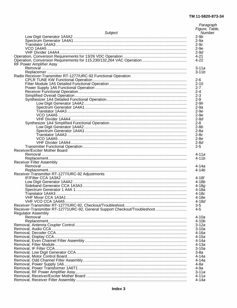
TM 11-5820-873-34
ParagraphFigure, Table,
Subject NumberLow Digit Generator 1A4A2...................................................................................................... 2-9bSpectrum Generator 1A4A1 ..................................................................................................... 2-9aTranslator 1A4A3 ..................................................................................................................... 2-9cVCO 1A4A5 ............................................................................................................................. 2-9eVHF Divider 1A4A4.................................................................................................................. 2-9d
Operation, Conversion Requirements for 13/26 VDC Operation ......................................................... 4-21Operation, Conversion Requirements for 115,230/132,264 VAC Operation ........................................ 4-22RF Power Amplifier Assy
Removal .................................................................................................................................. 3-11aReplacemer ............................................................................................................................. 3-11b
Radio Receiver-Transmitter RT-1277/URC-92 Functional OperationCPLR TUNE KW Functional Operation .................................................................................... 2-6Filter Module 1A5 Detailed Functional Operation ..................................................................... 2-10Power Supply 1A6 Functional Operation .................................................................................. 2-7Receiver Functional Operation................................................................................................. 2-4Simplified Overall Operation .................................................................................................... 2-3Synthesizer 1A4 Detailed Functional Operation........................................................................ 2-9
Low Digit Generator 1A4A2............................................................................................ 2-9hSpectrum Generator 1A4A1 ........................................................................................... 2-9aTranslator 1A4A3 ........................................................................................................... 2-9eVCO 1A4A5 ................................................................................................................... 2-9eVHF Divider 1A4A4........................................................................................................ 2-8d
Synthesizer 1A4 Simplified Functional Operation ..................................................................... 2-8Low Digit Generator 1A4A2............................................................................................ 2-8bSpectrum Generator 1A4A1 ........................................................................................... 2-8aTranslator 1A4A3 ........................................................................................................... 2-8cVCO 1A4A5 ................................................................................................................... 2-8eVHF Divider 1A4A4........................................................................................................ 2-8d
Transmitter Functional Operation ............................................................................................. 2-5Receiver/Exciter Mother Board
Removal .................................................................................................................................. 4-11aReplacement............................................................................................................................ 4-11b
Receiver Filter AssemblyRemoval .................................................................................................................................. 4-14aReplacement............................................................................................................................ 4-14b
Receiver-Transmitter RT-1277/URC-92 AdjustmentsIF/Filter CCA 1A3A2 ................................................................................................................ 4-18fLow Digit Generator 1A4A2...................................................................................................... 4-18bSideband Generator CCA 1A3A3 ............................................................................................. 4-18gSpectrum Generator 1 A4A 1 ................................................................................................... 4-18aTranslator 1A4A3 ..................................................................................................................... 4-18cVHF Mixer CCA 1A3A1............................................................................................................ 4-18eVHF VCO CCA 1A4A5............................................................................................................. 4-18d
Receiver-Transmitter RT-1277/URC-92, Checkout/Troubleshoot........................................................ 3-5Receiver-Transmitter RT-12771URC-92, General Support Checkout/Troubleshoot ............................ 4-5Regulator Assembly
Removal .................................................................................................................................. 4-10aReplacement............................................................................................................................ 4-10b
Removal, Antenna Coupler Control .................................................................................................... 3-12aRemoval, Audio CCA ......................................................................................................................... 3-10aRemoval, Decoder CCA..................................................................................................................... 4-16aRemoval, Display CCA....................................................................................................................... 4-15aRemoval, Even Channel Filter Assembly ........................................................................................... 4-14aRemoval, Filter Module ...................................................................................................................... 4-13aRemoval, IF Filter CCA...................................................................................................................... 3-10aRemoval, Low Digit Generator CCA................................................................................................... 3-8aRemoval, Motor Control Board........................................................................................................... 4-14aRemoval, Odd Channel Filter Assembly............................................................................................. 4-14aRemoval, Power Supply 1A6.............................................................................................................. 4-8aRemoval, Power Transformer 1A6T1 ................................................................................................. 4-9aRemoval, RF Power Amplifier Assy.................................................................................................... 3-11aRemoval, Receiver/Exciter Mother Board .......................................................................................... 4-11aRemoval, Receiver Filter Assembly ................................................................................................... 4-14a
Index 3
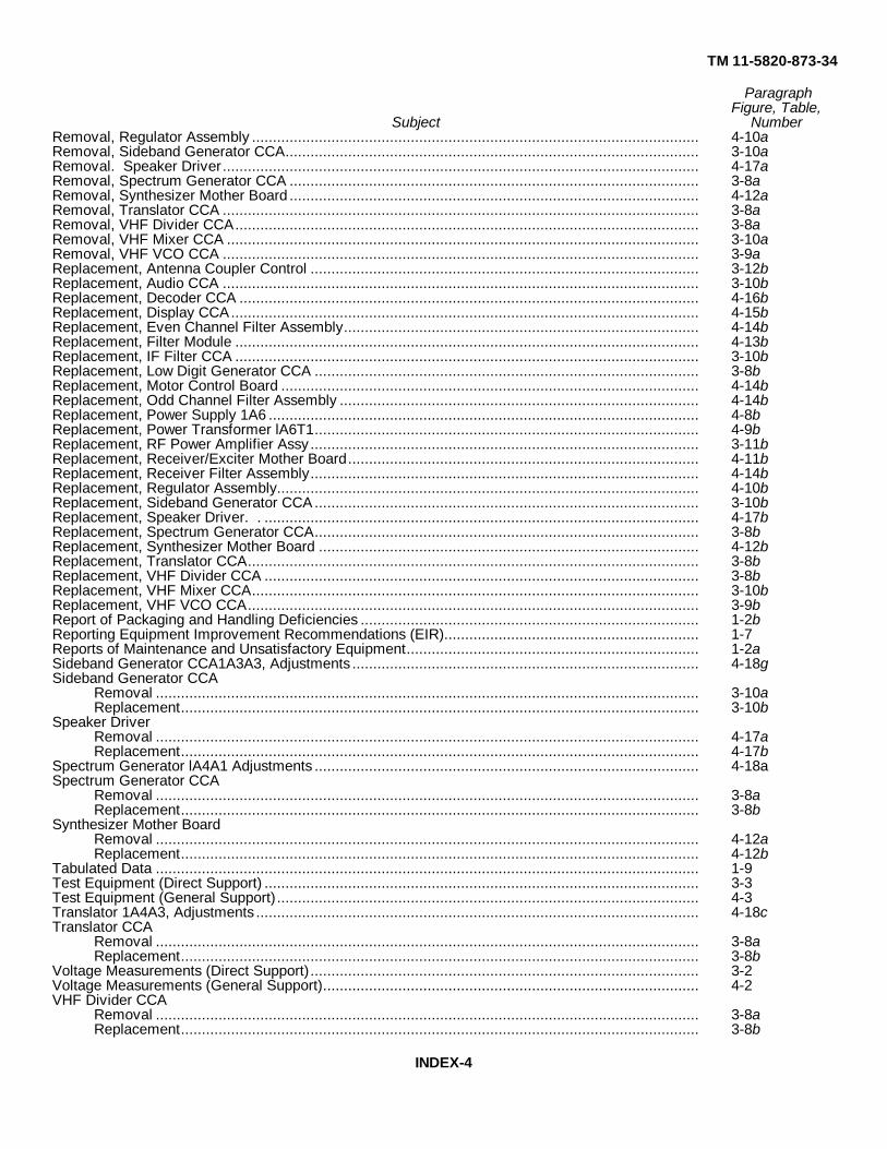
TM 11-5820-873-34
ParagraphFigure, Table,
Subject NumberRemoval, Regulator Assembly ........................................................................................................... 4-10aRemoval, Sideband Generator CCA................................................................................................... 3-10aRemoval. Speaker Driver.................................................................................................................. 4-17aRemoval, Spectrum Generator CCA .................................................................................................. 3-8aRemoval, Synthesizer Mother Board .................................................................................................. 4-12aRemoval, Translator CCA .................................................................................................................. 3-8aRemoval, VHF Divider CCA............................................................................................................... 3-8aRemoval, VHF Mixer CCA ................................................................................................................. 3-10aRemoval, VHF VCO CCA .................................................................................................................. 3-9aReplacement, Antenna Coupler Control ............................................................................................. 3-12bReplacement, Audio CCA .................................................................................................................. 3-10bReplacement, Decoder CCA .............................................................................................................. 4-16bReplacement, Display CCA................................................................................................................ 4-15bReplacement, Even Channel Filter Assembly..................................................................................... 4-14bReplacement, Filter Module ............................................................................................................... 4-13bReplacement, IF Filter CCA ............................................................................................................... 3-10bReplacement, Low Digit Generator CCA ............................................................................................ 3-8bReplacement, Motor Control Board .................................................................................................... 4-14bReplacement, Odd Channel Filter Assembly ...................................................................................... 4-14bReplacement, Power Supply 1A6 ....................................................................................................... 4-8bReplacement, Power Transformer lA6T1............................................................................................ 4-9bReplacement, RF Power Amplifier Assy ............................................................................................. 3-11bReplacement, Receiver/Exciter Mother Board.................................................................................... 4-11bReplacement, Receiver Filter Assembly............................................................................................. 4-14bReplacement, Regulator Assembly..................................................................................................... 4-10bReplacement, Sideband Generator CCA ............................................................................................ 3-10bReplacement, Speaker Driver. . ........................................................................................................ 4-17bReplacement, Spectrum Generator CCA............................................................................................ 3-8bReplacement, Synthesizer Mother Board ........................................................................................... 4-12bReplacement, Translator CCA............................................................................................................ 3-8bReplacement, VHF Divider CCA ........................................................................................................ 3-8bReplacement, VHF Mixer CCA........................................................................................................... 3-10bReplacement, VHF VCO CCA............................................................................................................ 3-9bReport of Packaging and Handling Deficiencies ................................................................................. 1-2bReporting Equipment Improvement Recommendations (EIR)............................................................. 1-7Reports of Maintenance and Unsatisfactory Equipment...................................................................... 1-2aSideband Generator CCA1A3A3, Adjustments ................................................................................... 4-18gSideband Generator CCA
Removal .................................................................................................................................. 3-10aReplacement............................................................................................................................ 3-10b
Speaker DriverRemoval .................................................................................................................................. 4-17aReplacement............................................................................................................................ 4-17b
Spectrum Generator lA4A1 Adjustments ............................................................................................ 4-18aSpectrum Generator CCA
Removal .................................................................................................................................. 3-8aReplacement............................................................................................................................ 3-8b
Synthesizer Mother BoardRemoval .................................................................................................................................. 4-12aReplacement............................................................................................................................ 4-12b
Tabulated Data .................................................................................................................................. 1-9Test Equipment (Direct Support) ........................................................................................................ 3-3Test Equipment (General Support) ..................................................................................................... 4-3Translator 1A4A3, Adjustments .......................................................................................................... 4-18cTranslator CCA
Removal .................................................................................................................................. 3-8aReplacement............................................................................................................................ 3-8b
Voltage Measurements (Direct Support) ............................................................................................. 3-2Voltage Measurements (General Support).......................................................................................... 4-2VHF Divider CCA
Removal .................................................................................................................................. 3-8aReplacement............................................................................................................................ 3-8b
INDEX-4
TM 11-5820-873-34
ParagraphFigure, Table,
Subject Number
VHF Mixer CCA 1A3A1, Adjustments................................................................................................. 4-18eVHF Mixer CCA
Removal .................................................................................................................................. 3-10aReplacement............................................................................................................................ 3-10b
VHF VCO CCA, Adjustments ............................................................................................................. 4-18dVHFVCOCCA
Removal. ................................................................................................................................. 3-9aReplacement............................................................................................................................ 3-9b
Warranty ............................................................................................................................................ 1-3
INDEX-5
U.S. GOVERNMENT PRINTING OFFICE : 1992 0 - 311-831 (44217)
FO-1 Receiver Block Diagram
FO-2 Transmitter Block Diagram
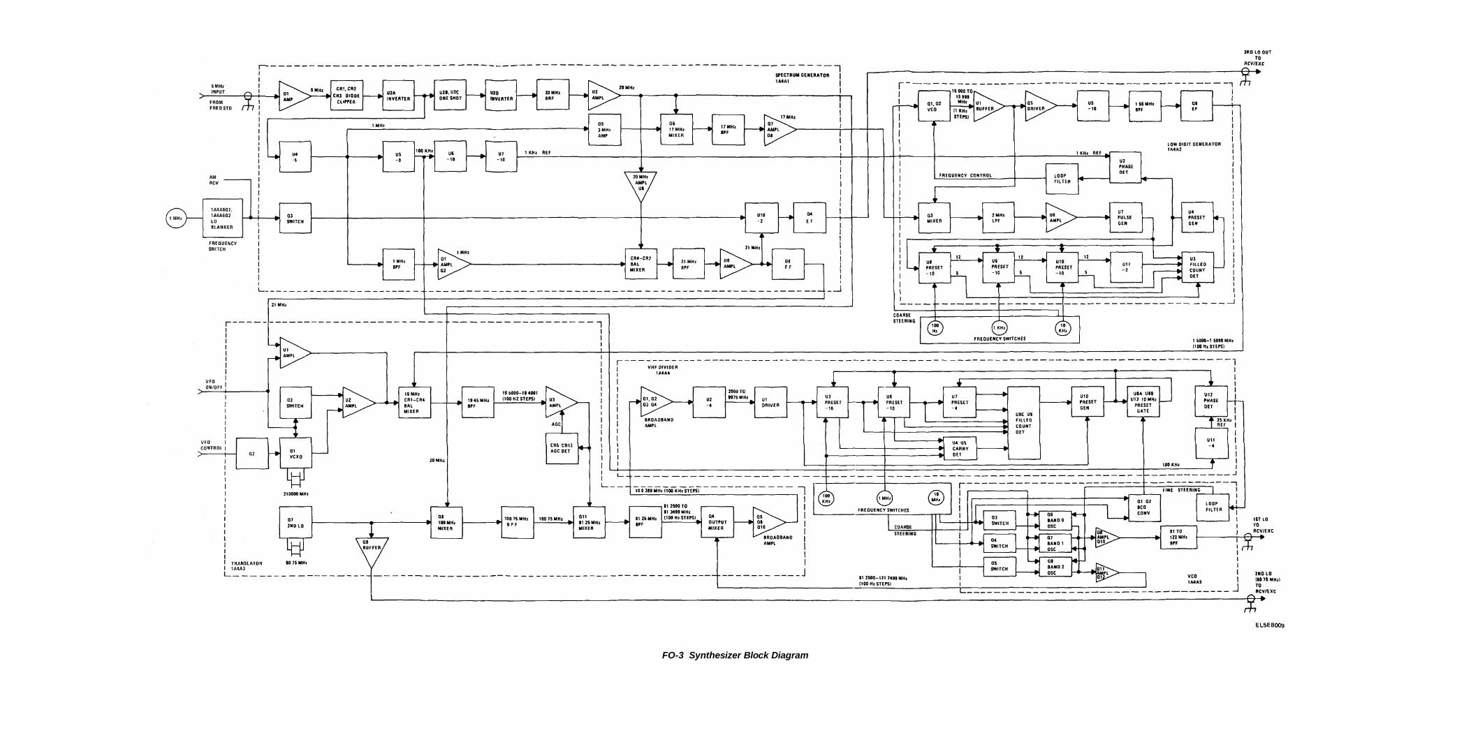
FO-3 Synthesizer Block Diagram
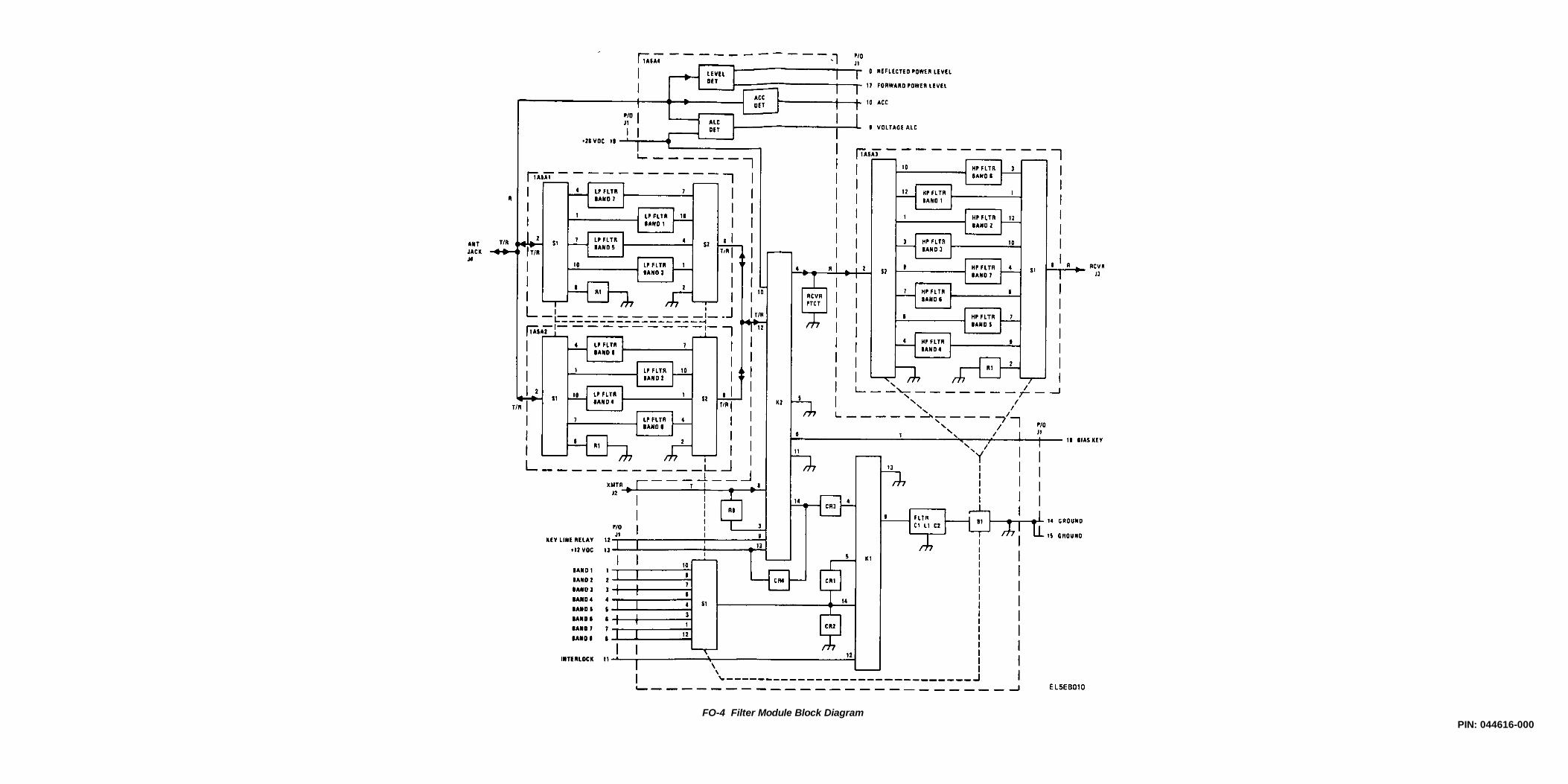
FO-4 Filter Module Block DiagramPIN: 044616-000
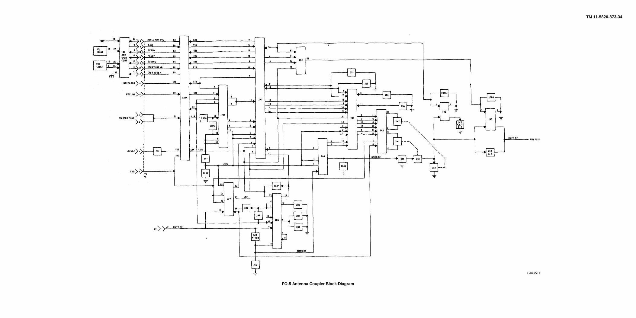
TM 11-5820-873-34
FO-5 Antenna Coupler Block Diagram
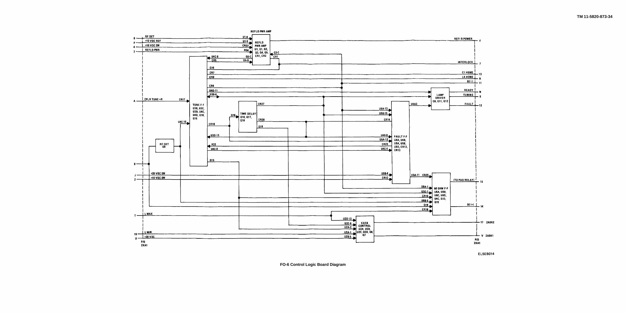
TM 11-5820-873-34
FO-6 Control Logic Board Diagram

TM 11-5820-873-34
FO-7 Phase & Amplitude Control Block Diagram
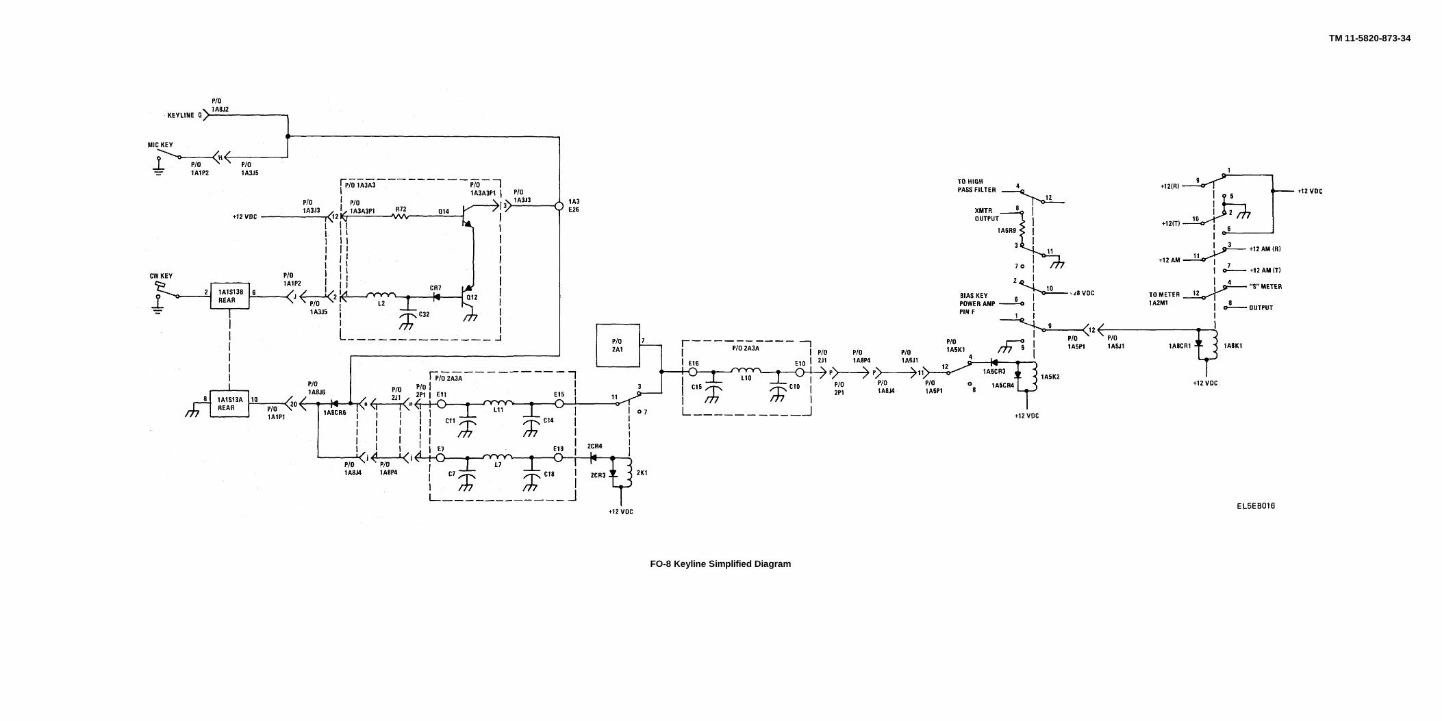
TM 11-5820-873-34
FO-8 Keyline Simplified Diagram
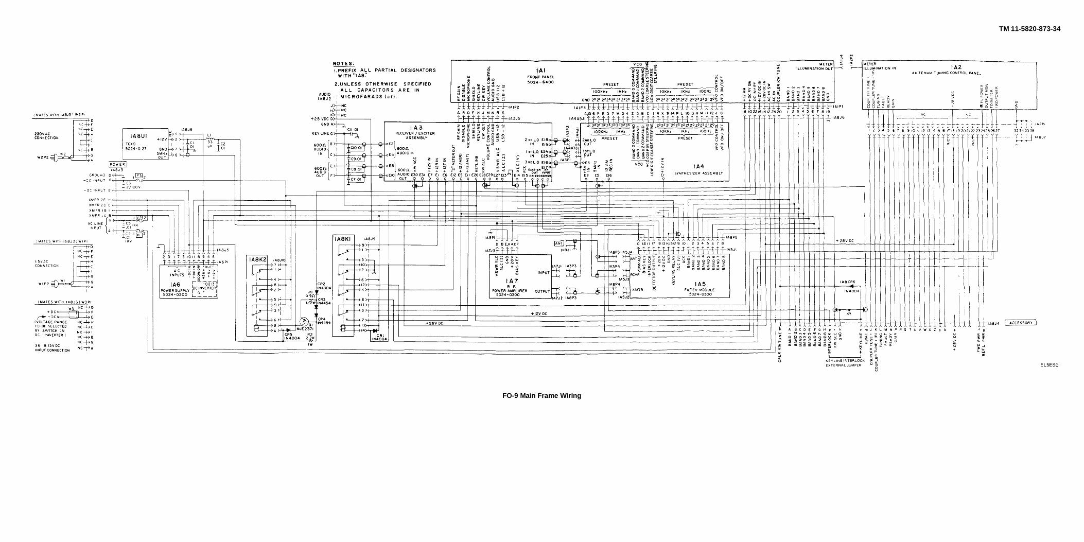
TM 11-5820-873-34
FO-9 Main Frame Wiring
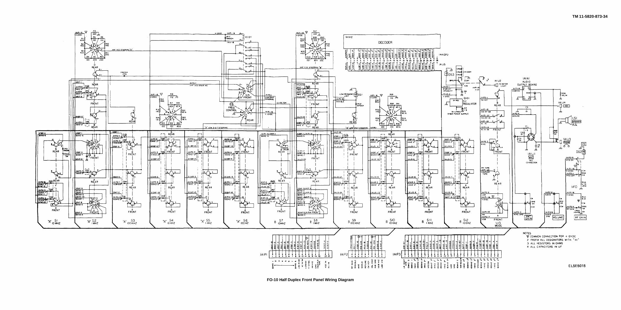
TM 11-5820-873-34
FO-10 Half Duplex Front Panel Wiring Diagram
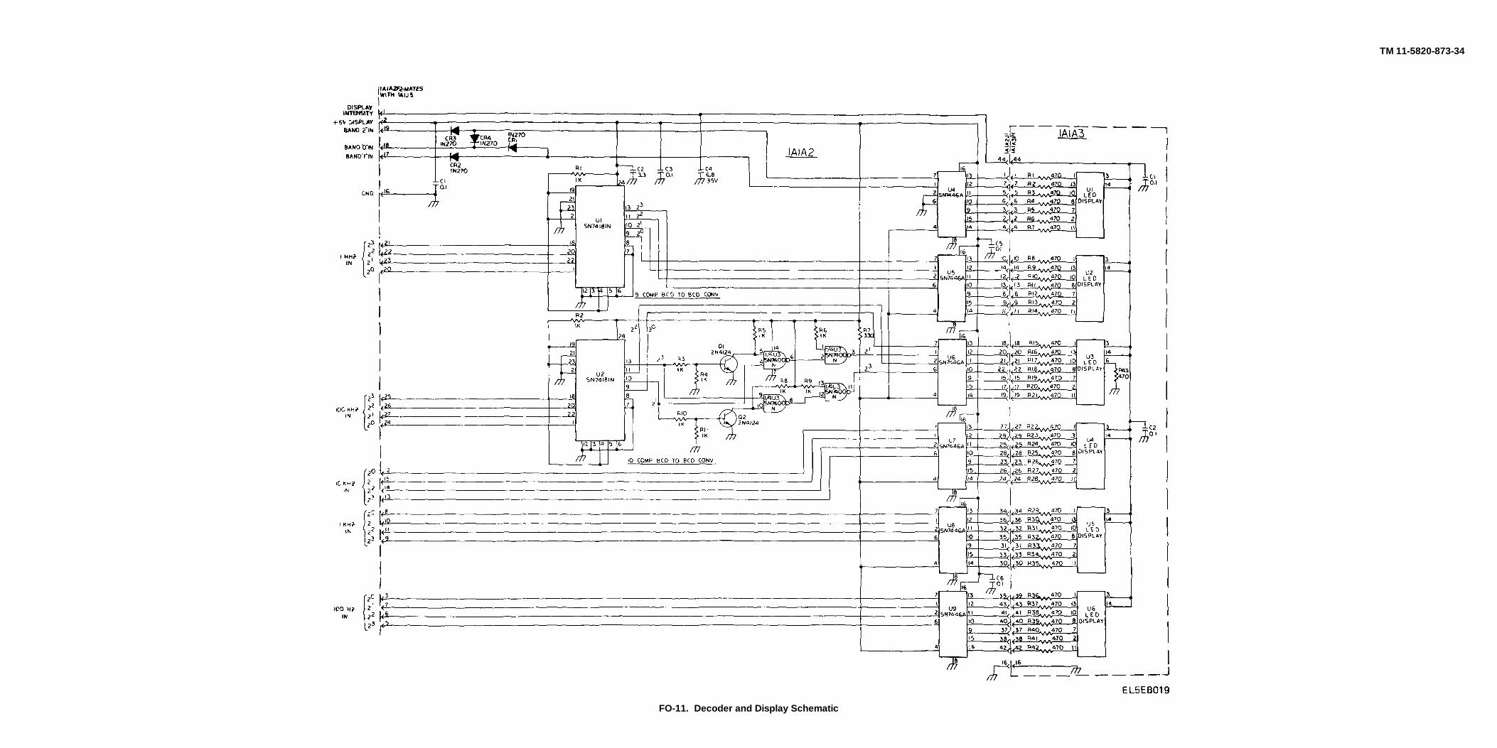
TM 11-5820-873-34
FO-11. Decoder and Display Schematic
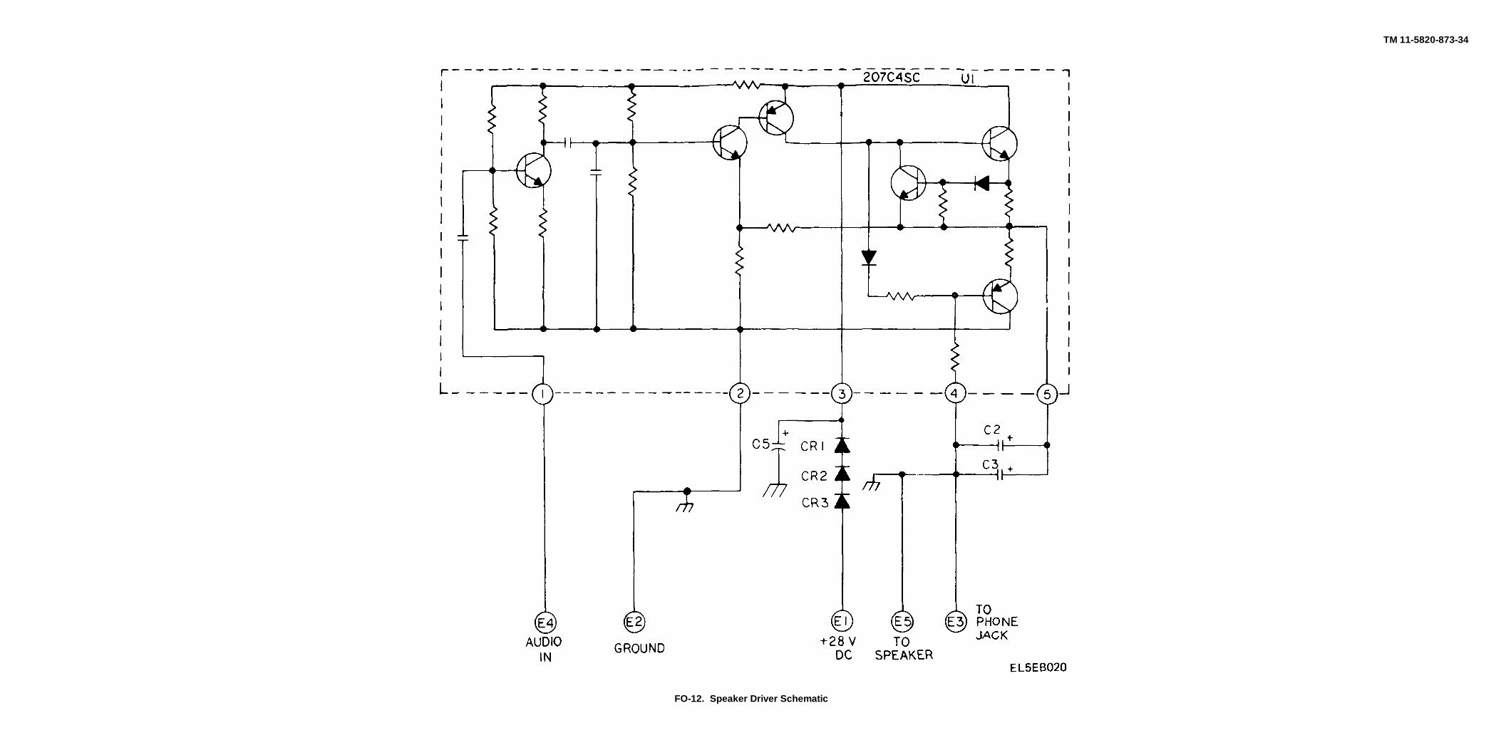
TM 11-5820-873-34
FO-12. Speaker Driver Schematic
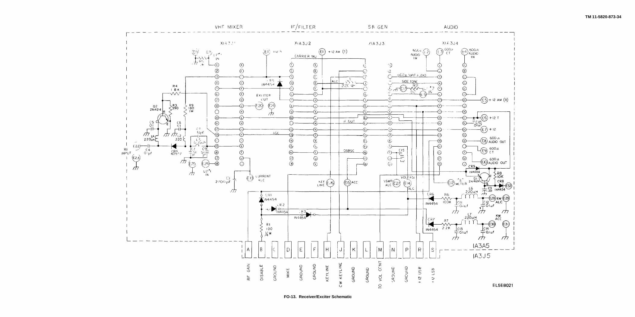
TM 11-5820-873-34
FO-13. Receiver/Exciter Schematic
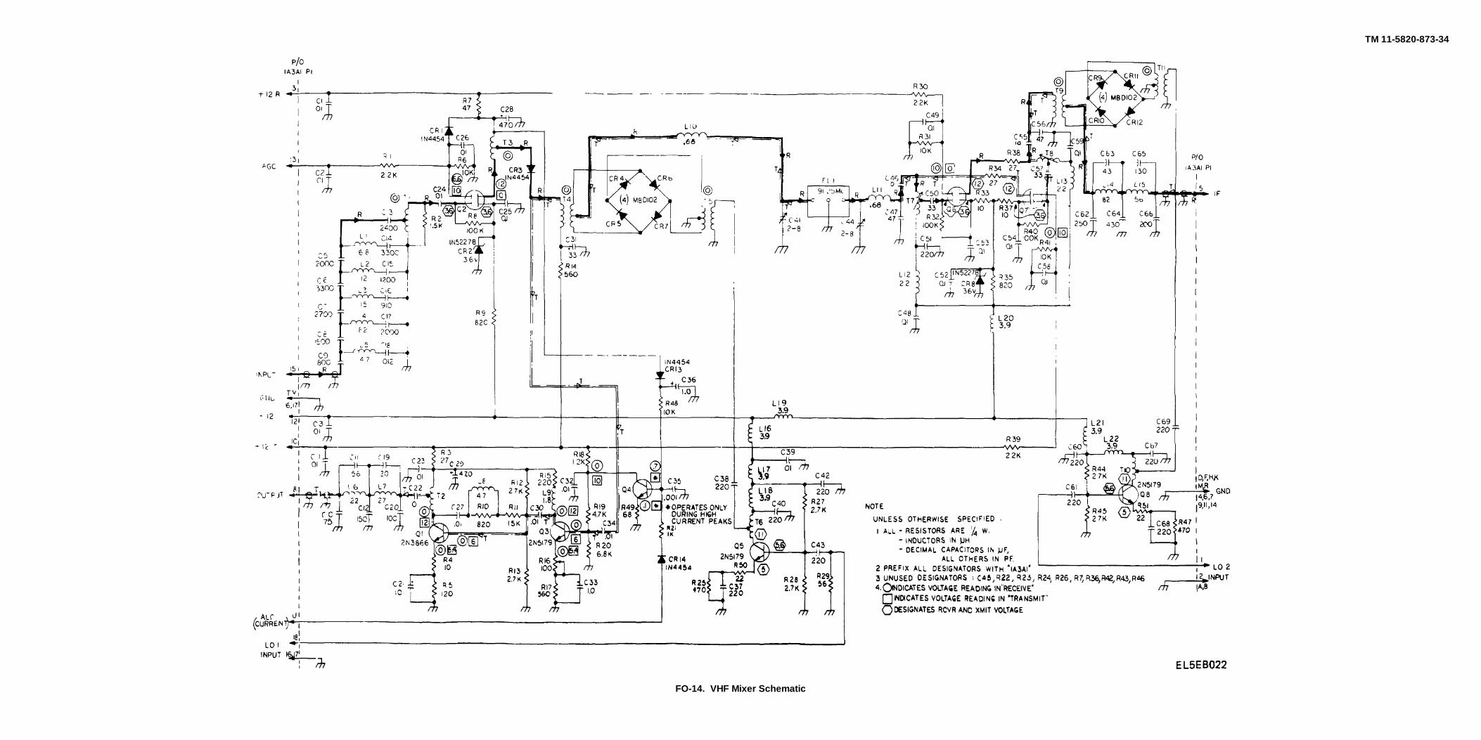
TM 11-5820-873-34
FO-14. VHF Mixer Schematic
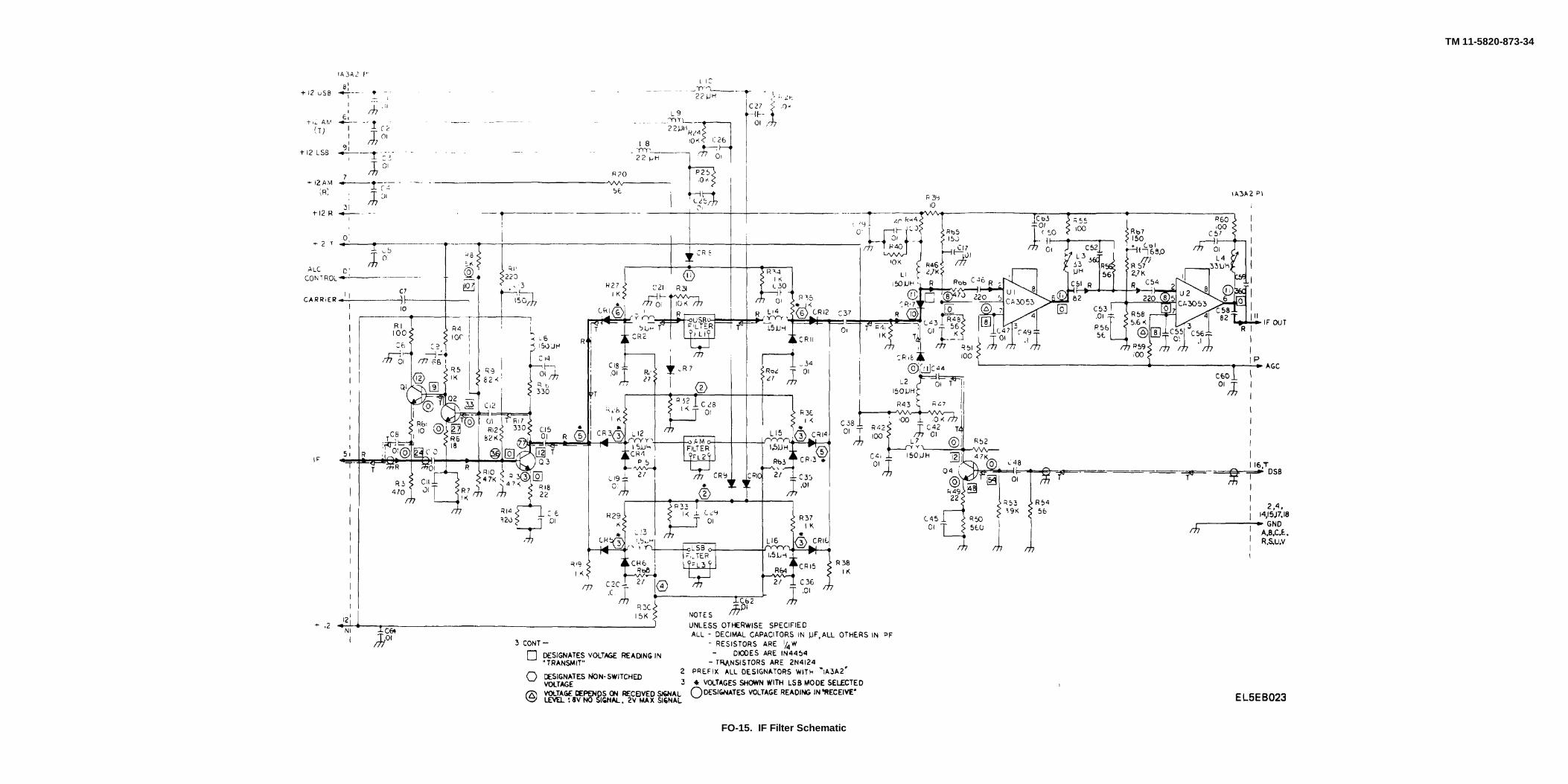
TM 11-5820-873-34
FO-15. IF Filter Schematic

FO-16. Sideband Generator Schematic
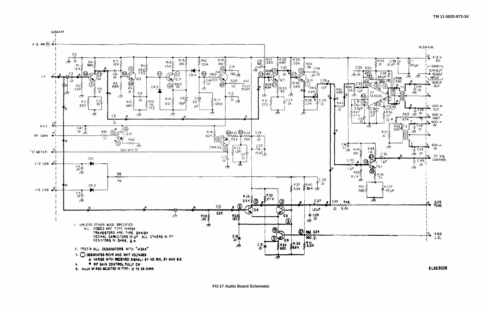
TM 11-5820-873-34
FO-17 Audio Board Schematic
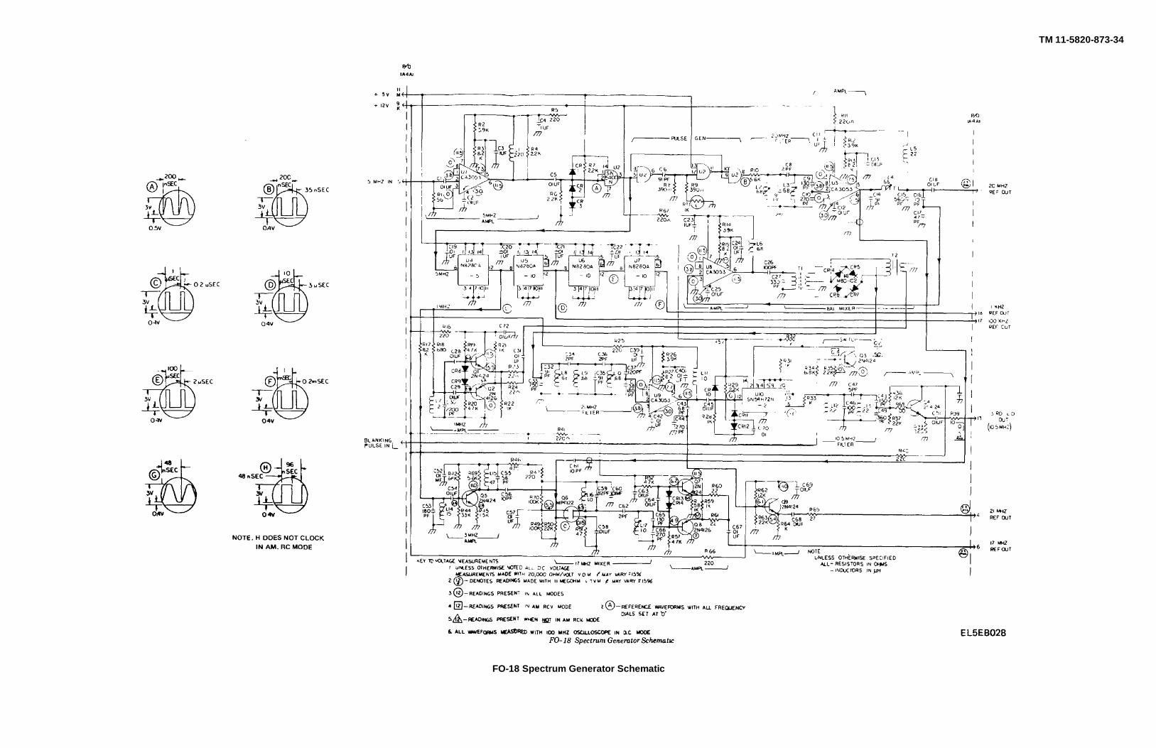
TM 11-5820-873-34
FO-18 Spectrum Generator Schematic
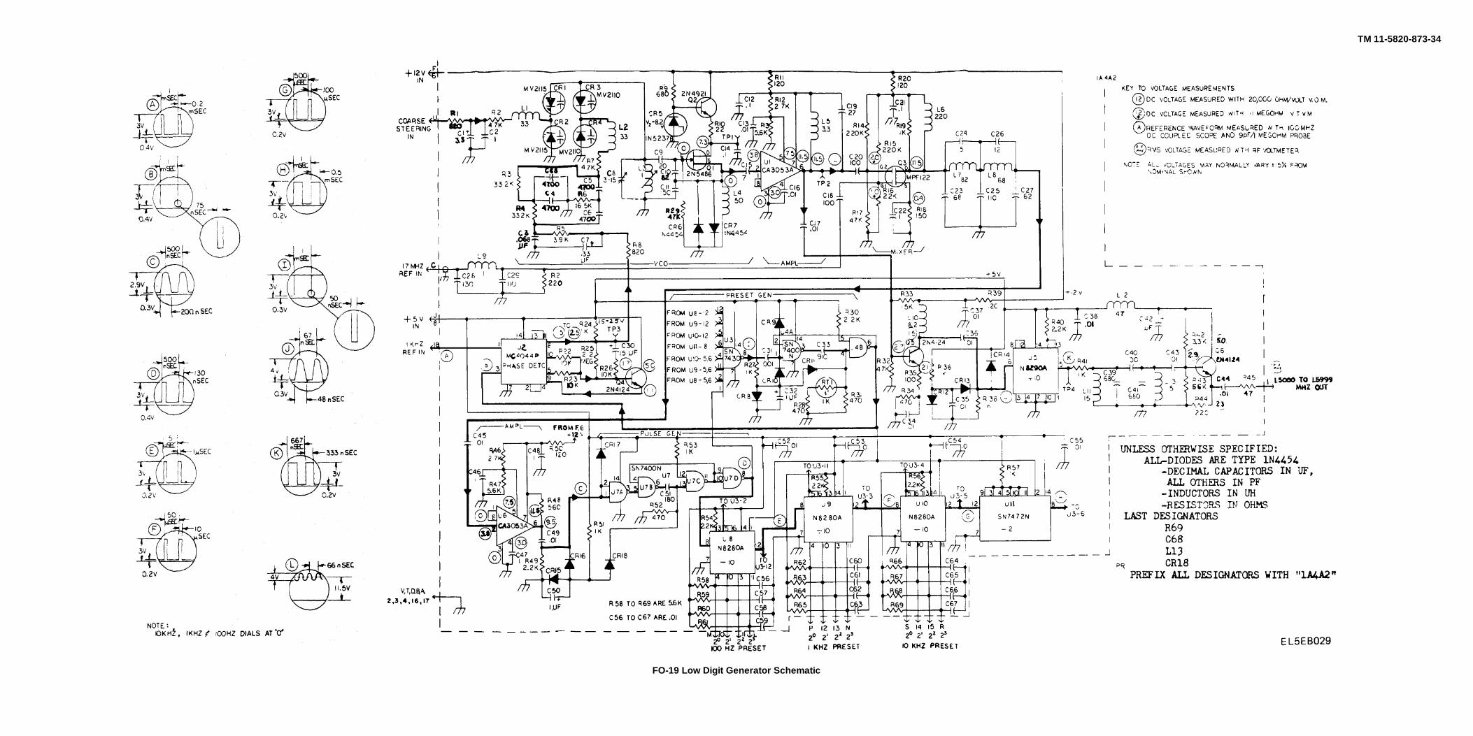
TM 11-5820-873-34
FO-19 Low Digit Generator Schematic
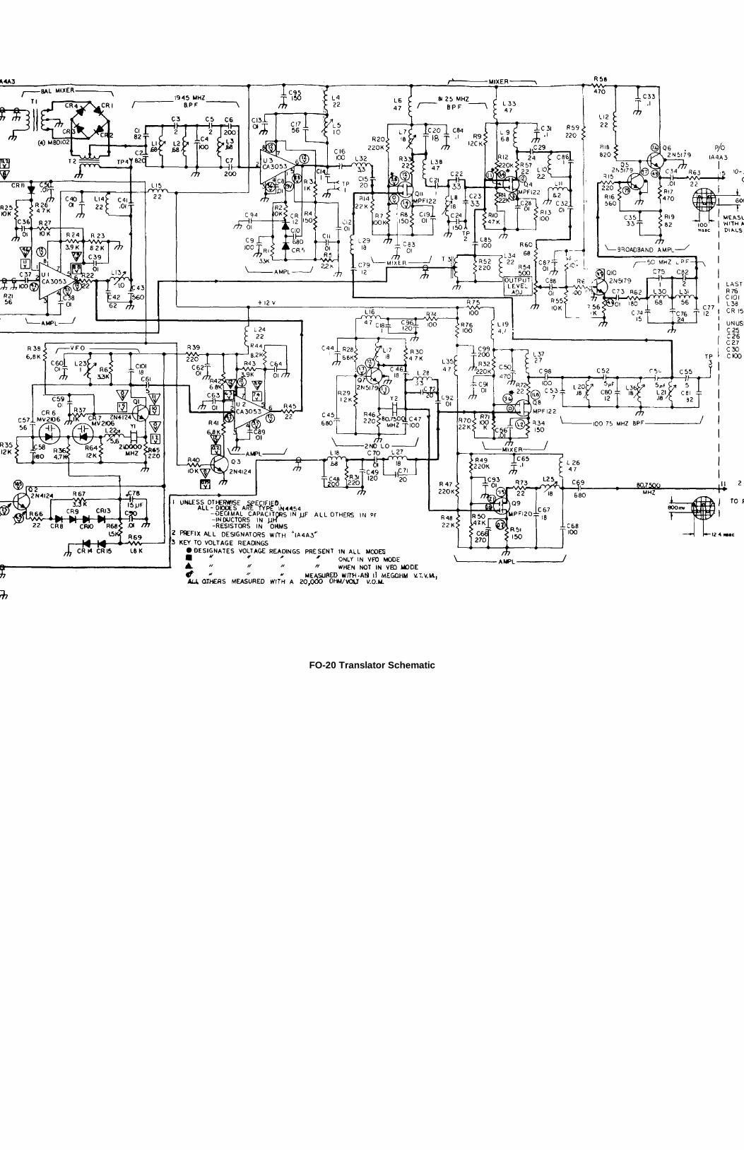
FO-20 Translator Schematic
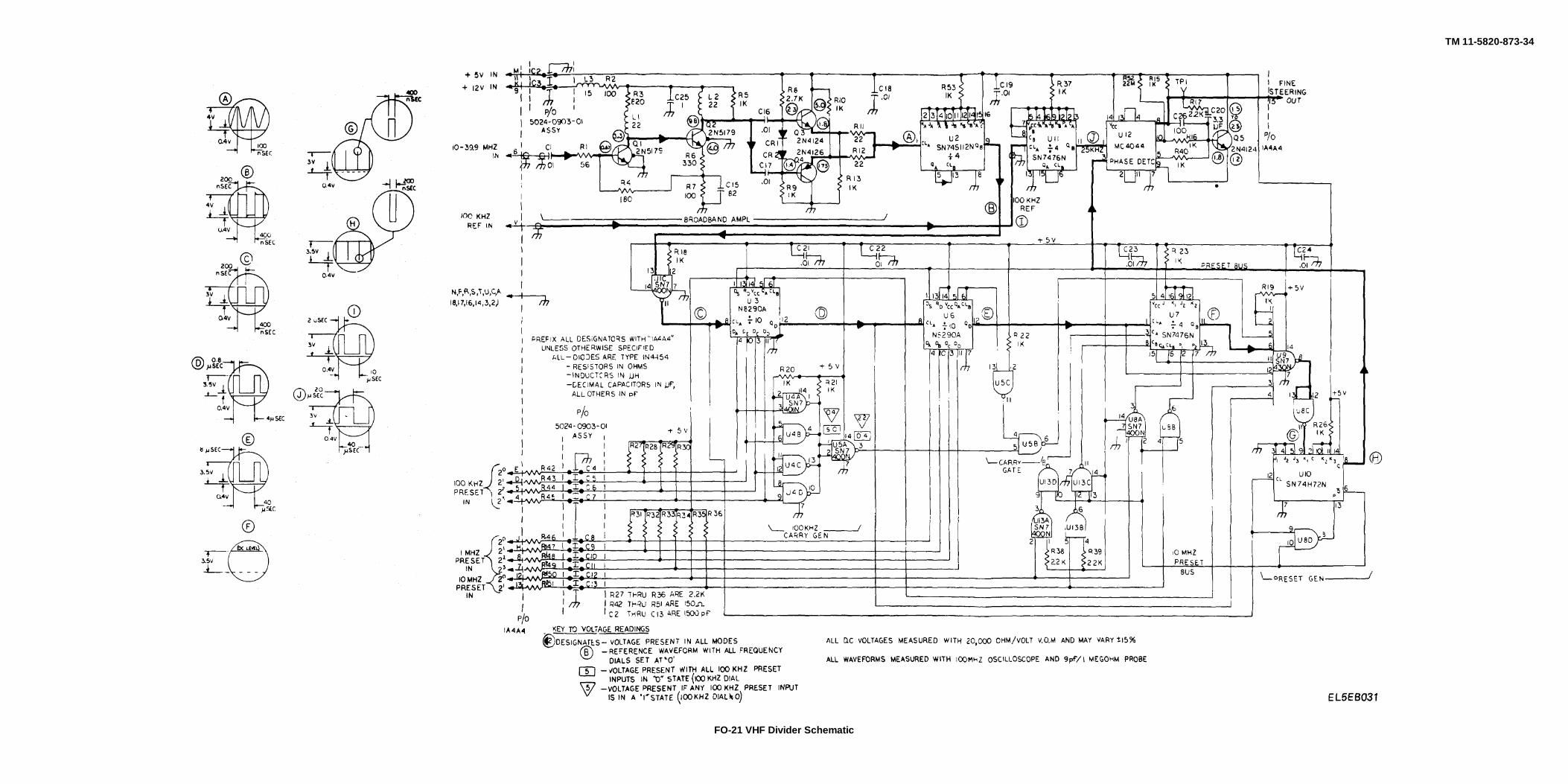
TM 11-5820-873-34
FO-21 VHF Divider Schematic
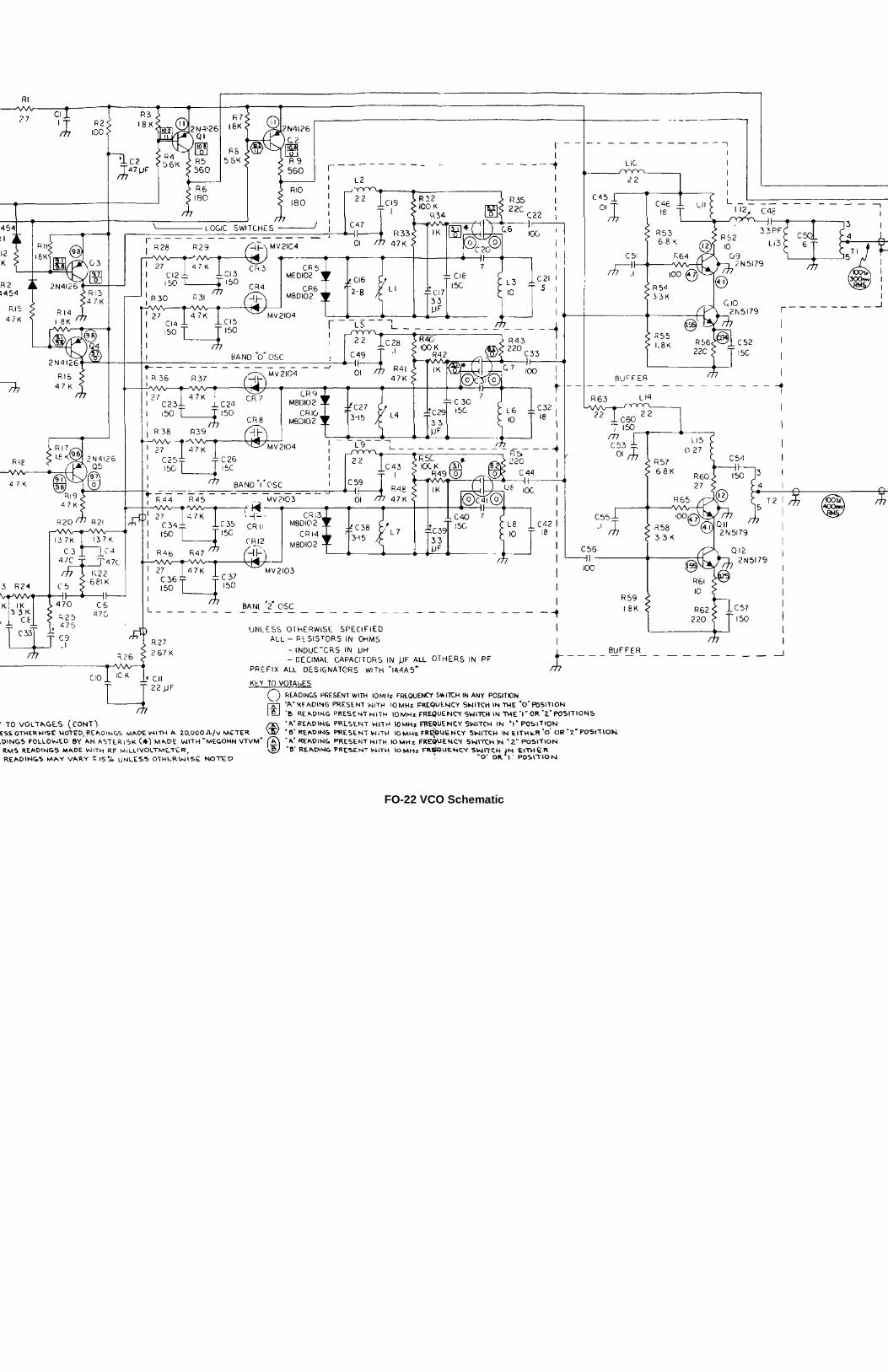
FO-22 VCO Schematic
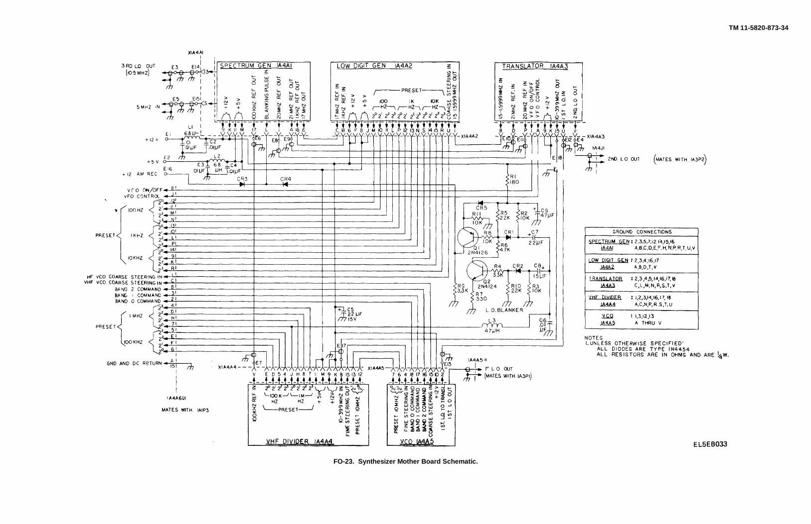
TM 11-5820-873-34
FO-23. Synthesizer Mother Board Schematic.
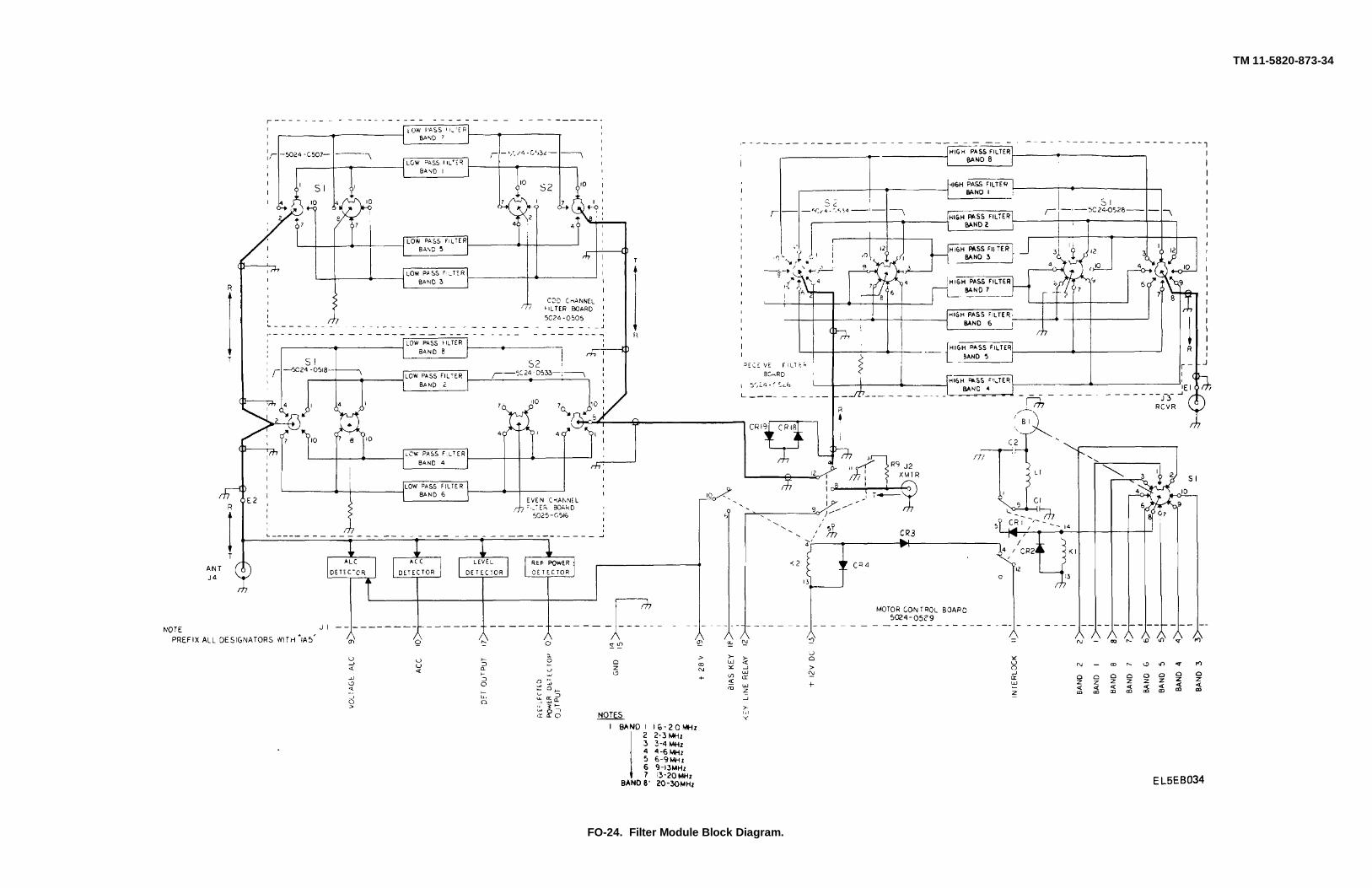
TM 11-5820-873-34
FO-24. Filter Module Block Diagram.
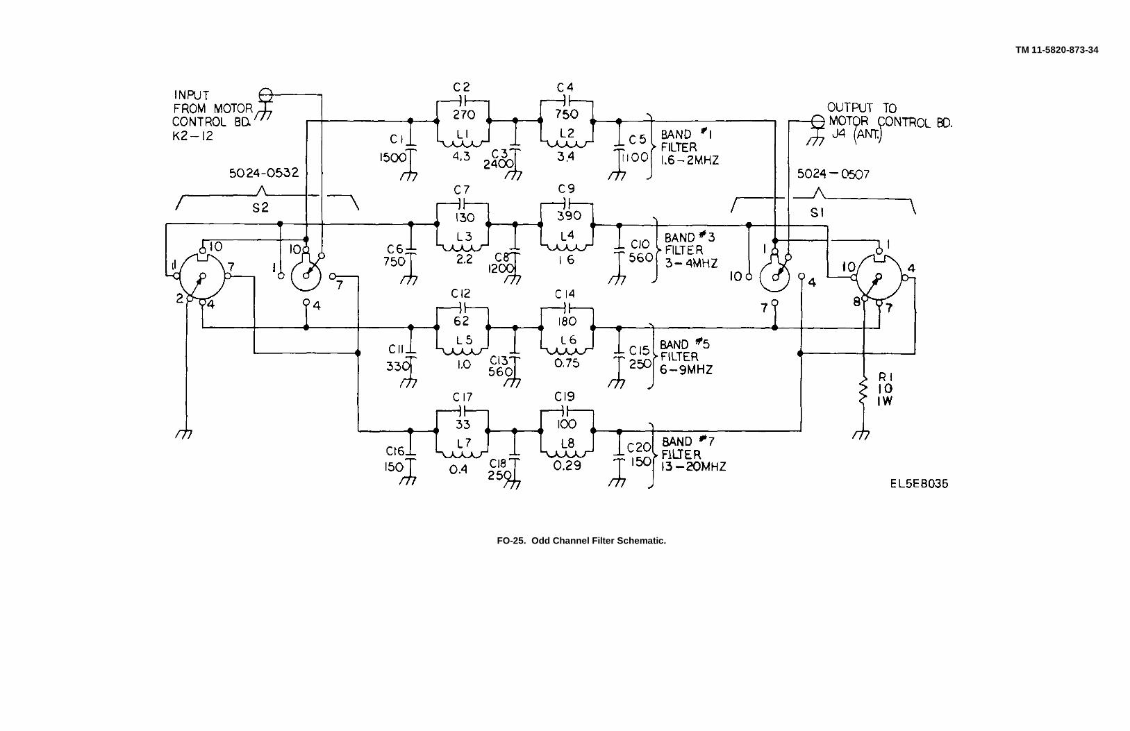
TM 11-5820-873-34
FO-25. Odd Channel Filter Schematic.
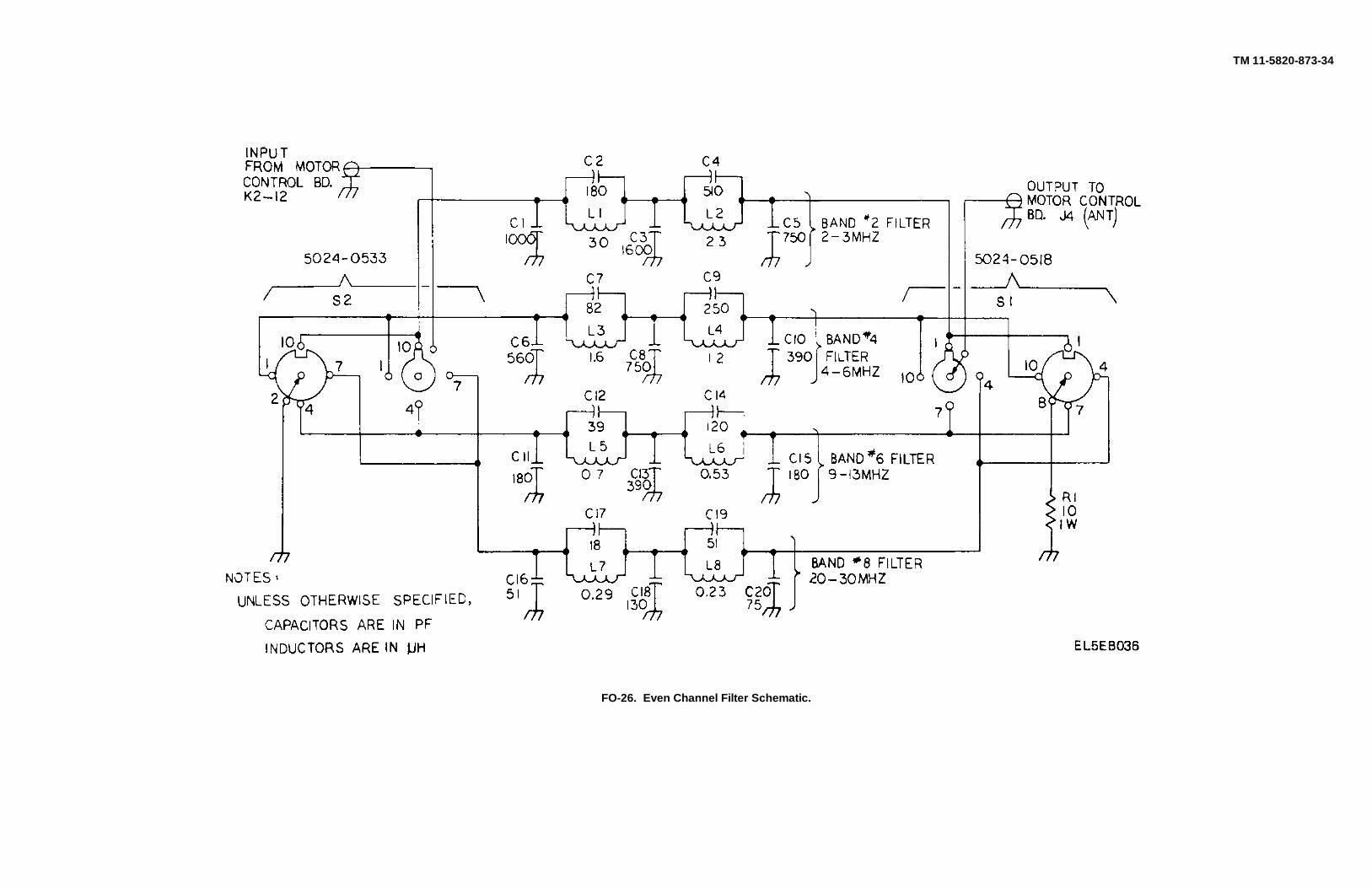
TM 11-5820-873-34
FO-26. Even Channel Filter Schematic.
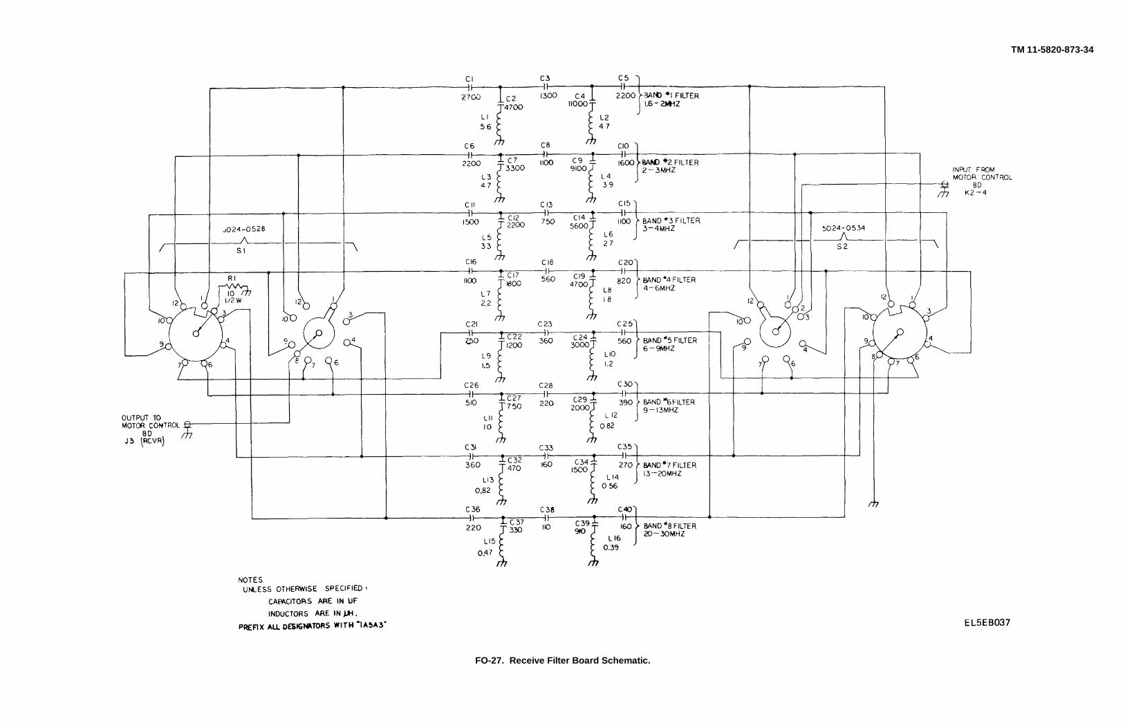
TM 11-5820-873-34
FO-27. Receive Filter Board Schematic.
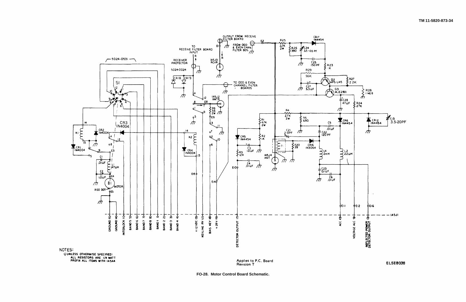
TM 11-5820-873-34
FO-28. Motor Control Board Schematic.
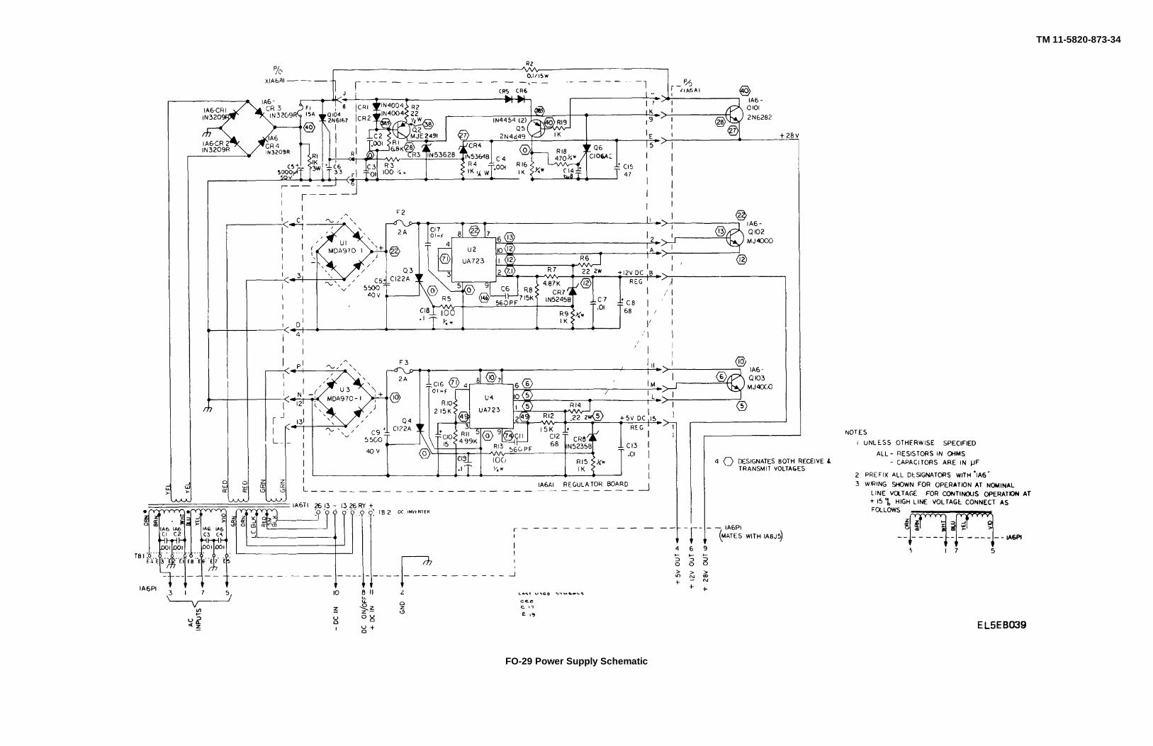
TM 11-5820-873-34
FO-29 Power Supply Schematic

TM 11-5820-873-34
FO-30 DC Inverter Schematic
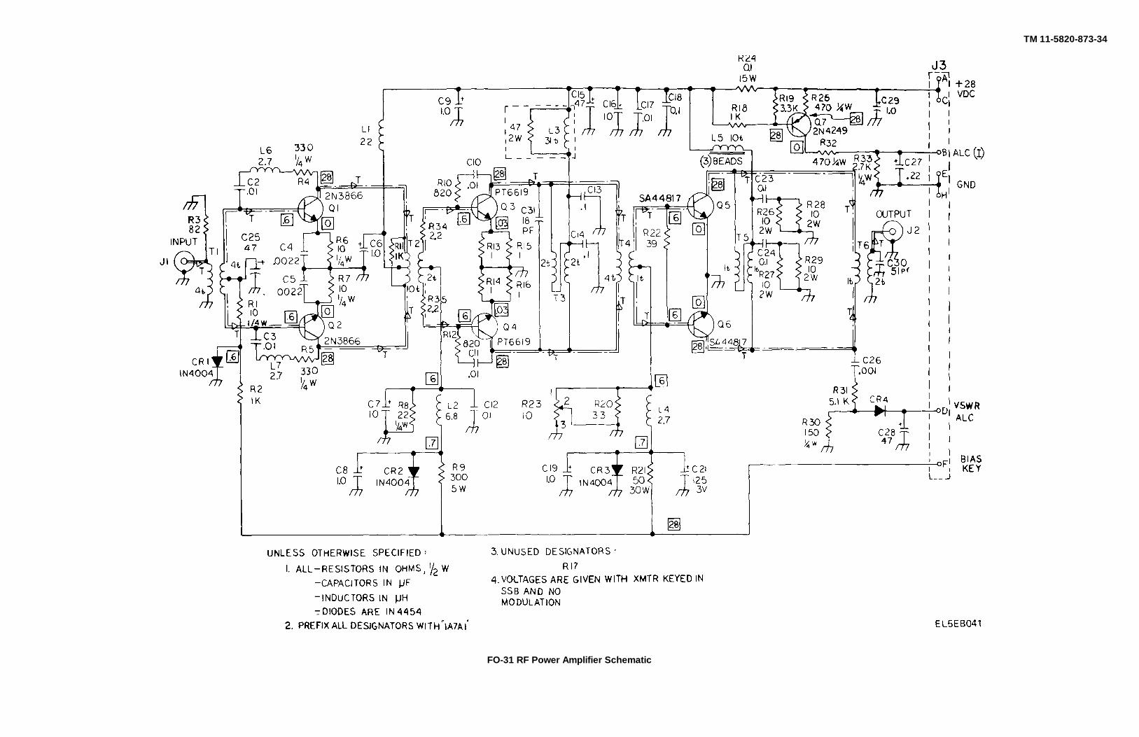
TM 11-5820-873-34
FO-31 RF Power Amplifier Schematic
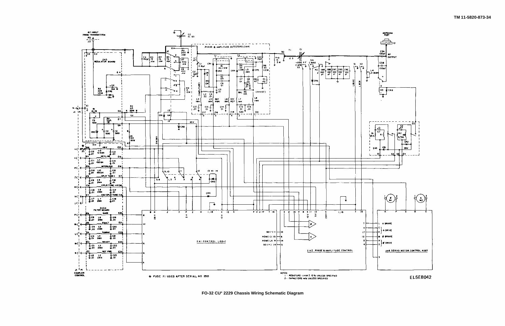
TM 11-5820-873-34
FO-32 CU° 2229 Chassis Wiring Schematic Diagram
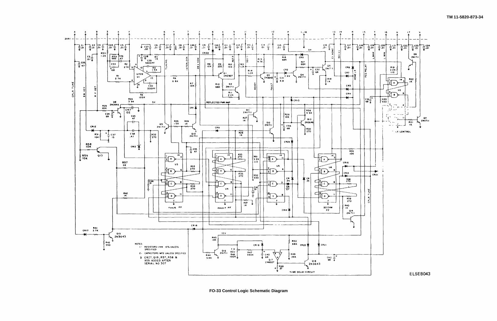
TM 11-5820-873-34
FO-33 Control Logic Schematic Diagram
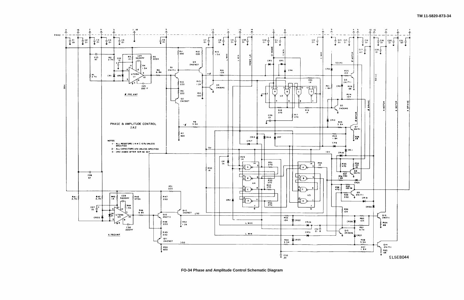
TM 11-5820-873-34
FO-34 Phase and Amplitude Control Schematic Diagram
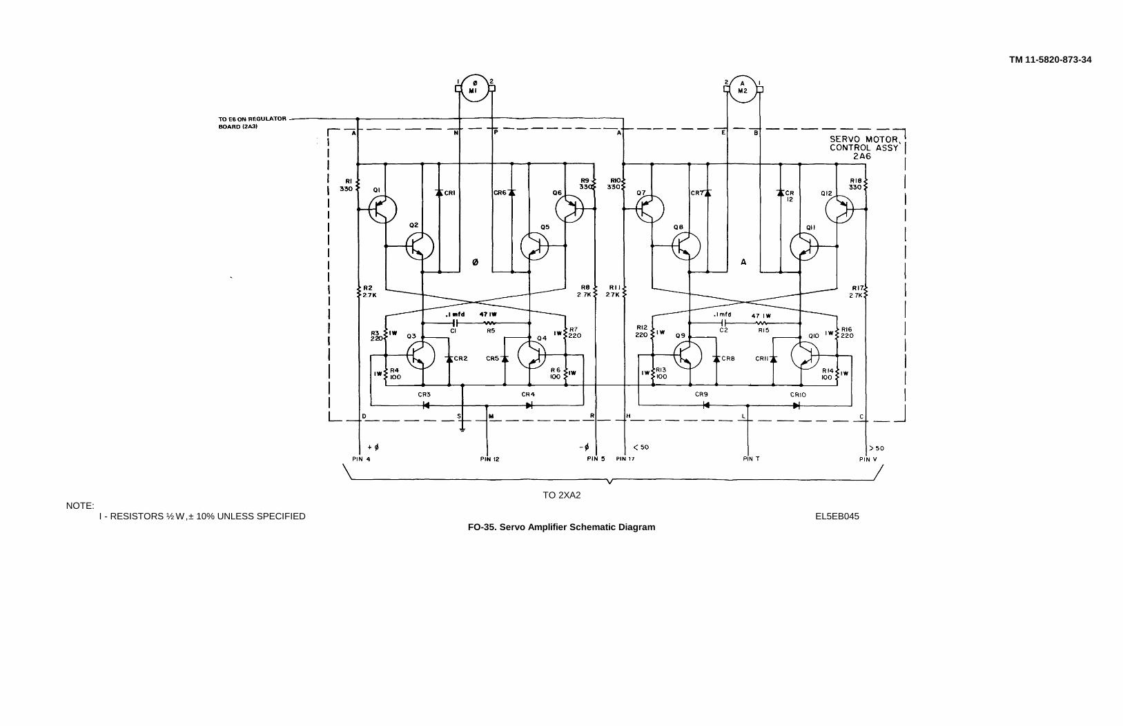
TM 11-5820-873-34
TO 2XA2NOTE:
I - RESISTORS ½ W,± 10% UNLESS SPECIFIED EL5EB045FO-35. Servo Amplifier Schematic Diagram
By Order of the Secretary of the Army:
E. C. MEYERGeneral, United States Army
Official: Chief of StaffJ C PENNINGTON
Major General, United States ArmyThe Adjutant General
DISTRIBUTION:Active Army
HISA(Ft Monmouth)(21)USAINSCOM (2)COE(1)TSG (1)USAARENBD (1)DARCOM (1)TRADOC (2)OS Maj Comd (4)TECOM (2)USACC (4)MDW (1)Armies (2)Corps (2)Svc Colleges (1)USASIGS (5)USAADS (2)USAFAS (2)USAARMS (2)USAIS (2)USAES (2)USAICS (3)MAAG (1)USARMIS (1)USAERDAA (1)USAERDAW (1)Ft Carson (5)Ft Gordon (10)Ft Gillem (10)Ft Richardson (CERCOM Ofc) (2)Army Dep(1)except
LBAD(14)SAAD (30)TOAD(14)SHAD (3)
USA Dep (1)Sig Sec USA Dep (1)Units org under fol TOE (2)
29-20729-610
NG: NoneUSAR: None
For explanation of abbreviations see, AR 310-50
The Metric System and Equivalents
Linear Measure Liquid Measure
1 centiliter = 10 milliters = .34 fl. ounce1 centimeter = 10 millimeters = .39 inch 1 deciliter = 10 centiliters = 3.38 fl. ounces1 decimeter = 10 centimeters = 3.94 inches 1 liter = 10 deciliters = 33.81 fl. ounces1 meter = 10 decimeters = 39.37 inches 1 dekaliter = 10 liters = 2.64 gallons1 dekameter = 10 meters = 32.8 feet 1 hectoliter = 10 dekaliters = 26.42 gallons1 hectometer = 10 dekameters = 328.08 feet 1 kiloliter = 10 hectoliters = 264.18 gallons1 kilometer = 10 hectometers = 3,280.8 feet
Square MeasureWeights
1 sq. centimeter = 100 sq. millimeters = .155 sq. inch1 centigram = 10 milligrams = .15 grain 1 sq. decimeter = 100 sq. centimeters = 15.5 sq. inches1 decigram = 10 centigrams = 1.54 grains 1 sq. meter (centare) = 100 sq. decimeters = 10.76 sq. feet1 gram = 10 decigram = .035 ounce 1 sq. dekameter (are) = 100 sq. meters = 1,076.4 sq. feet1 decagram = 10 grams = .35 ounce 1 sq. hectometer (hectare) = 100 sq. dekameters = 2.47 acres1 hectogram = 10 decagrams = 3.52 ounces 1 sq. kilometer = 100 sq. hectometers = .386 sq. mile1 kilogram = 10 hectograms = 2.2 pounds1 quintal = 100 kilograms = 220.46 pounds Cubic Measure1 metric ton = 10 quintals = 1.1 short tons
1 cu. centimeter = 1000 cu. millimeters = .06 cu. inch1 cu. decimeter = 1000 cu. centimeters = 61.02 cu. inches1 cu. meter = 1000 cu. decimeters = 35.31 cu. feet
Approximate Conversion Factors
To change To Multiply by To change To Multiply by
inches centimeters 2.540 ounce-inches Newton-meters .007062feet meters .305 centimeters inches .394yards meters .914 meters feet 3.280miles kilometers 1.609 meters yards 1.094square inches square centimeters 6.451 kilometers miles .621square feet square meters .093 square centimeters square inches .155square yards square meters .836 square meters square feet 10.764square miles square kilometers 2.590 square meters square yards 1.196acres square hectometers .405 square kilometers square miles .386cubic feet cubic meters .028 square hectometers acres 2.471cubic yards cubic meters .765 cubic meters cubic feet 35.315fluid ounces milliliters 29,573 cubic meters cubic yards 1.308pints liters .473 milliliters fluid ounces .034quarts liters .946 liters pints 2.113gallons liters 3.785 liters quarts 1.057ounces grams 28.349 liters gallons .264pounds kilograms .454 grams ounces .035short tons metric tons .907 kilograms pounds 2.205pound-feet Newton-meters 1.356 metric tons short tons 1.102pound-inches Newton-meters .11296
Temperature (Exact)
°F Fahrenheit 5/9 (after Celsius °Ctemperature subtracting 32) temperature

PIN: 044616-000