Embed Size (px)
Citation preview

Load (A)
Effi
cien
cy (
%)
60
70
80
90
100
1m 10m 100m 1 5
D008
VOUT = 1.2 VVOUT = 1.8 VVOUT = 3.3 V
TLV62085
2.5V to 6VR1138k
R2110k
VIN
POWER GOOD
VOS
FB
VIN
GND
EN
SW
PG
C222µF
R31M
VOUT
1.8V
L10.47µH
C110µF
Product
Folder
Order
Now
Technical
Documents
Tools &
Software
Support &Community
An IMPORTANT NOTICE at the end of this data sheet addresses availability, warranty, changes, use in safety-critical applications,intellectual property matters and other important disclaimers. PRODUCTION DATA.
TLV62085SLVSD63B –OCTOBER 2015–REVISED JULY 2018
TLV62085 High Efficiency 3-A Step-Down Converter in 2-mm × 2-mm VSON Package
1
1 Features1• DCS-Control™ Topology• Up to 95% Efficiency• 17-μA Operating Quiescent Current• 31mΩ and 23mΩ Power MOSFET Switch• 2.5-V to 6.0-V Input Voltage Range• 0.8-V to VIN Adjustable Output Voltage• Power Save Mode for Light Load Efficiency• 100% Duty Cycle for Lowest Dropout• Hiccup Short-Circuit Protection• Output Discharge• Power Good Output• Thermal Shutdown Protection• Available in 2-mm × 2-mm VSON Package• For Improved Feature Set, See TPS62085• Create a Custom Design using the TLV62085 with
the WEBENCH® Power Designer
2 Applications• Battery-Powered Applications• Point-of-Load• Processor Supplies• Hard Disk Drives (HDD) / Solid State Drives
(SSD)
3 DescriptionThe TLV62085 device is a high-frequencysynchronous step-down converter optimized for smallsolution size and high efficiency. With an inputvoltage range of 2.5 V to 6.0 V, common batterytechnologies are supported. The devices focus onhigh-efficiency step-down conversion over a wideoutput current range. At medium to heavy loads, theconverter operates in PWM mode and automaticallyenters Power Save Mode operation at light load tomaintain high efficiency over the entire load currentrange.
To address the requirements of system power rails,the internal compensation circuit allows a largeselection of external output capacitor values rangingfrom 10 µF to 150 µF and above. Together with itsDCS-Control™ architecture, excellent load transientperformance and output voltage regulation accuracyare achieved. The device is available in a 2-mm × 2-mm VSON package.
Device Information(1)
PART NUMBER PACKAGE BODY SIZE (NOM)TLV62085 VSON (7) 2.00 mm × 2.00 mm
(1) For all available packages, see the orderable addendum atthe end of the data sheet.
spacer
spacer
spacerTypical Application Schematic
Efficiency at VIN = 5 V

2
TLV62085SLVSD63B –OCTOBER 2015–REVISED JULY 2018 www.ti.com
Product Folder Links: TLV62085
Submit Documentation Feedback Copyright © 2015–2018, Texas Instruments Incorporated
Table of Contents1 Features .................................................................. 12 Applications ........................................................... 13 Description ............................................................. 14 Revision History..................................................... 25 Pin Configuration and Functions ......................... 36 Specifications......................................................... 4
6.1 Absolute Maximum Ratings ...................................... 46.2 ESD Ratings.............................................................. 46.3 Recommended Operating Conditions....................... 46.4 Thermal Information .................................................. 46.5 Electrical Characteristics.......................................... 56.6 Typical Characteristics .............................................. 5
7 Detailed Description .............................................. 67.1 Overview ................................................................... 67.2 Functional Block Diagram ......................................... 67.3 Feature Description................................................... 77.4 Device Functional Modes.......................................... 8
8 Application and Implementation .......................... 98.1 Application Information.............................................. 98.2 Typical Application ................................................... 9
9 Power Supply Recommendations ...................... 1510 Layout................................................................... 15
10.1 Layout Guidelines ................................................. 1510.2 Layout Example .................................................... 1510.3 Thermal Considerations ........................................ 15
11 Device and Documentation Support ................. 1611.1 Development Support ........................................... 1611.2 Documentation Support ........................................ 1611.3 Receiving Notification of Documentation Updates 1611.4 Community Resources.......................................... 1611.5 Trademarks ........................................................... 1611.6 Electrostatic Discharge Caution............................ 1711.7 Glossary ................................................................ 17
12 Mechanical, Packaging, and OrderableInformation ........................................................... 17
4 Revision History
Changes from Revision A (January 2017) to Revision B Page
• Added Figure 3 to power save mode section......................................................................................................................... 7
Changes from Original (October 2015) to Revision A Page
• Added WEBENCH™ information and hyperlinks to Features, Detailed Design Procedure, and Device Support sections .. 1• Added SW (AC) to the Absolute Maximum Rating table ....................................................................................................... 4• Added Table 1, PG Pin Logic ................................................................................................................................................. 8

GND
SWFB
VIN
PG
VOS
EN
4
3
1
5
6
7
2
3
TLV62085www.ti.com SLVSD63B –OCTOBER 2015–REVISED JULY 2018
Product Folder Links: TLV62085
Submit Documentation FeedbackCopyright © 2015–2018, Texas Instruments Incorporated
5 Pin Configuration and Functions
RLT Package7-Pin VSON
Top View
Pin FunctionsPIN
I/O DESCRIPTIONNAME NO.EN 1 IN Device enable pin. To enable the device, this pin needs to be pulled high. Pulling this pin low disables the
device. This pin has a pulldown resistor of typically 400 kΩ when the device is disabled.FB 3 IN Feedback pin. Connect a resistor divider to set the output voltage.GND 5 Ground pin.PG 2 OUT Power good open drain output pin. The pullup resistor can not be connected to any voltage higher than 6 V. If
unused, leave it floating.SW 6 PWR Switch pin of the power stage.VIN 7 PWR Input voltage pin.VOS 4 IN Output voltage sense pin. This pin must be directly connected to the output capacitor.

4
TLV62085SLVSD63B –OCTOBER 2015–REVISED JULY 2018 www.ti.com
Product Folder Links: TLV62085
Submit Documentation Feedback Copyright © 2015–2018, Texas Instruments Incorporated
(1) Stresses beyond those listed under Absolute Maximum Ratings may cause permanent damage to the device. These are stress ratingsonly and functional operation of the device at these or any other conditions beyond those indicated under Recommended OperatingConditions is not implied. Exposure to absolute–maximum–rated conditions for extended periods may affect device reliability.
(2) All voltage values are with respect to network ground terminal.(3) While switching.
6 Specifications
6.1 Absolute Maximum Ratings (1)
MIN MAX UNIT
Voltage at Pins (2)
VIN, FB, VOS, EN, PG – 0.3 7VSW (DC) – 0.3 VIN + 0.3
SW (AC, less than 100ns) (3) – 3 11
TemperatureOperating Junction, TJ – 40 150 °CStorage, Tstg – 65 150 °C
(1) JEDEC document JEP155 states that 500-V HBM allows safe manufacturing with a standard ESD control process.(2) JEDEC document JEP157 states that 250-V CDM allows safe manufacturing with a standard ESD control process.
6.2 ESD RatingsVALUE UNIT
V(ESD) Electrostatic dischargeHuman body model (HBM), per ANSI/ESDA/JEDEC JS-001 (1) ±2000
VCharged device model (CDM), per JEDEC specification JESD22-C101 (2) ±500
(1) Refer to Application and Implementation for further information.
6.3 Recommended Operating Conditions (1)
MIN NOM MAX UNITVIN Input voltage range 2.5 6 VVOUT Output voltage range 0.8 VIN VISINK_PG Sink current at PG pin 1 mAVPG Pullup resistor voltage 6 VTJ Operating junction temperature –40 125 °C
(1) For more information about traditional and new thermal metrics, see the Semiconductor and IC Package Thermal Metrics applicationreport.
6.4 Thermal Information
THERMAL METRIC (1)TLV62085
UNITRLT [VSON]7 PINS
RθJA Junction-to-ambient thermal resistance 107.8 °C/WRθJC(top) Junction-to-case (top) thermal resistance 66.2 °C/WRθJB Junction-to-board thermal resistance 17.1 °C/WψJT Junction-to-top characterization parameter 2.1 °C/WψJB Junction-to-board characterization parameter 17.1 °C/WRθJC(bot) Junction-to-case (bottom) thermal resistance N/A °C/W

Load (A)
Sw
itchi
ng F
requ
ency
(H
z)
103
104
105
106
5x10⁶
1m 10m 100m 1 5
D007
VIN = 2.5 VVIN = 3.6 VVIN = 6.0 V
5
TLV62085www.ti.com SLVSD63B –OCTOBER 2015–REVISED JULY 2018
Product Folder Links: TLV62085
Submit Documentation FeedbackCopyright © 2015–2018, Texas Instruments Incorporated
6.5 Electrical CharacteristicsTJ = 25 °C, and VIN = 3.6 V, unless otherwise noted.
PARAMETER TEST CONDITIONS MIN TYP MAX UNITSUPPLYIQ Quiescent current into VIN No load, device not switching 17 µAISD Shutdown current into VIN EN = Low 0.7 µA
VUVLOUnder voltage lock out threshold VIN falling 2.1 2.2 2.3 VUnder voltage lock out hysteresis VIN rising 200 mV
TJSDThermal shutdown threshold TJ rising 150 °CThermal shutdown hysteresis TJ falling 20 °C
LOGIC INTERFACE ENVIH High-level input voltage VIN = 2.5 V to 6.0 V 1.0 VVIL Low-level input voltage VIN = 2.5 V to 6.0 V 0.4 VIEN,LKG Input leakage current into EN pin EN = High 0.01 µARPD Pull-down resistance at EN pin EN = Low 400 kΩSOFT START, POWER GOODtSS Soft start time Time from EN high to 95% of VOUT nominal 0.8 ms
VPG Power good thresholdVOUT rising, referenced to VOUT nominal 95%VOUT falling, referenced to VOUT nominal 90%
VPG,OL Low-level output voltage Isink = 1 mA 0.4 VIPG,LKG Input leakage current into PG pin VPG = 5.0 V 0.01 µAOUTPUT
VFB Feedback regulation voltage PWM mode, 2.5 V ≤ VIN ≤ 6 VTJ = 0°C to 85 °C 792 800 808 mV
IFB,LKG Feedback input leakage current VFB = 1 V 0.01 µARDIS Output discharge resistor EN = LOW, VOUT = 1.8 V 260 ΩPOWER SWITCH
RDS(on)High-side FET on-resistance ISW = 500 mA 31 mΩLow-side FET on-resistance ISW = 500 mA 23 mΩ
ILIM High-side FET switch current limit 3.7 4.6 5.5 AfSW PWM switching frequency IOUT = 1 A 2.4 MHz
6.6 Typical Characteristics
VOUT = 1.2 VFigure 1. Switching Frequency

VOS
FB
GND
Output DischargeLogic
260Ω
Direct Controland
CompensationTimer
ton
Comparator
Ramp
Error AmplifierDCS - Control
TM
MOSFET DriverControl Logic
High SideCurrent Sense
HiccupCounter
SW
VIN
EN
BandgapUndervoltage Lockout
Thermal ShutdownEN
PG
VFB
VREF
VREF
400kΩ(1)
Note:(1) When the device is enabled, the 400 k resistor is disconnected.Ω
6
TLV62085SLVSD63B –OCTOBER 2015–REVISED JULY 2018 www.ti.com
Product Folder Links: TLV62085
Submit Documentation Feedback Copyright © 2015–2018, Texas Instruments Incorporated
7 Detailed Description
7.1 OverviewThe TLV62085 synchronous step-down converter is based on the DCS-Control (Direct Control with Seamlesstransition into Power Save Mode) topology. This is an advanced regulation topology that combines theadvantages of hysteretic, voltage, and current mode control schemes.
The DCS-Control topology operates in PWM (pulse width modulation) mode for medium to heavy load conditionsand in Power Save Mode at light load currents. In PWM mode, the converter operates with its nominal switchingfrequency of 2.4 MHz, having a controlled frequency variation over the input voltage range. As the load currentdecreases, the converter enters Power Save Mode, reducing the switching frequency and minimizing the IC'scurrent consumption to achieve high efficiency over the entire load current range. Because DCS-Control supportsboth operation modes (PWM and PFM) within a single building block, the transition from PWM mode to PowerSave Mode is seamless and without effects on the output voltage. The device offers both excellent DC voltageand superior load transient regulation, combined with very low output voltage ripple, minimizing interference withRF circuits.
7.2 Functional Block Diagram
Figure 2. Functional Block Diagram

IN,MIN OUT OUT,MAX DS(on) LV V I (R + R )= + ´
tON
IINDUCTOR
VOUT
tPAUSE
OUTON
IN
OUTPFM
2 IN OUTINON
OUT
Vt 420 ns
V
2 If
V VVt
V L
= ´
´
=
-
´ ´
7
TLV62085www.ti.com SLVSD63B –OCTOBER 2015–REVISED JULY 2018
Product Folder Links: TLV62085
Submit Documentation FeedbackCopyright © 2015–2018, Texas Instruments Incorporated
7.3 Feature Description
7.3.1 Power Save ModeAs the load current decreases, the TLV62085 enters Power Save Mode (PSM) operation. During Power SaveMode, the converter operates with reduced switching frequency and with a minimum quiescent currentmaintaining high efficiency. Power Save Mode occurs when the inductor current becomes discontinuous. PowerSave Mode is based on a fixed on-time architecture, as related in Equation 1. The switching frequency over thewhole load current range is also shown in Figure 1 for a shown typical application.
(1)
In PSM, the output voltage rises slightly above the nominal output voltage, as shown in Figure 10. This effect isminimized by increasing the output capacitor or inductor value.
During PAUSE period in PSM (shown in Figure 3), the device does not change the PG pin state nor does itdetect an UVLO event, in order to achieve a minimum quiescent current and maintain high efficiency at lightloads.
Figure 3. Power Save Mode Waveform Diagram
7.3.2 100% Duty Cycle Low Dropout OperationThe device offers low input-to-output voltage difference by entering 100% duty cycle mode. In this mode, thehigh-side MOSFET switch is constantly turned on and the low-side MOSFET is switched off. This is particularlyuseful in battery powered applications to achieve the longest operation time by taking full advantage of the wholebattery voltage range. The minimum input voltage to maintain output regulation, depending on the load currentand output voltage can be calculated as:
with• VIN,MIN = Minimum input voltage to maintain an output voltage• IOUT,MAX = Maximum output current• RDS(on) = High-side FET ON-resistance• RL = Inductor ohmic resistance (DCR) (2)
7.3.3 Soft StartThe TLV62085 has an internal soft-start circuitry which monotonically ramps up the output voltage and reachesthe nominal output voltage during a soft-start time of typically 0.8 ms. This avoids excessive inrush current andcreates a smooth output voltage slope. It also prevents excessive voltage drops of primary cells andrechargeable batteries with high internal impedance. The device is able to start into a prebiased output capacitor.The device starts with the applied bias voltage and ramps the output voltage to its nominal value.

8
TLV62085SLVSD63B –OCTOBER 2015–REVISED JULY 2018 www.ti.com
Product Folder Links: TLV62085
Submit Documentation Feedback Copyright © 2015–2018, Texas Instruments Incorporated
Feature Description (continued)7.3.4 Switch Current Limit and Hiccup Short-Circuit ProtectionThe switch current limit prevents the device from high inductor current and from drawing excessive current fromthe battery or input voltage rail. Excessive current might occur with a shorted or saturated inductor or a heavyload or shorted output circuit condition. If the inductor current reaches the threshold ILIM, the high-side MOSFETis turned off and the low-side MOSFET is turned on to ramp down the inductor current. When this switch currentlimits is triggered 32 times, the device stops switching and enables the output discharge. The device thenautomatically starts a new start-up after a typical delay time of 66 µs has passed. This is named HICCUP short-circuit protection. The device repeats this mode until the high load condition disappears.
7.3.5 Undervoltage LockoutTo avoid misoperation of the device at low input voltages, an undervoltage lockout (UVLO) is implemented,which shuts down the device at voltages lower than VUVLO with a hysteresis of 200 mV.
7.3.6 Thermal ShutdownThe device goes into thermal shutdown and stops switching when the junction temperature exceeds TJSD. Whenthe device temperature falls below the threshold by 20°C, the device returns to normal operation automatically.
7.4 Device Functional Modes
7.4.1 Enable and DisableThe device is enabled by setting the EN pin to a logic HIGH. Accordingly, shutdown mode is forced if the EN pinis pulled LOW with a shutdown current of typically 0.7 μA.
In shutdown mode, the internal power switches as well as the entire control circuitry are turned off. An internalresistor of 260 Ω discharges the output through the VOS pin smoothly. The output discharge function also workswhen thermal shutdown, UVLO, or short-circuit protection are triggered.
An internal pulldown resistor of 400 kΩ is connected to the EN pin when the EN pin is LOW. The pulldownresistor is disconnected when the EN pin is HIGH.
7.4.2 Power GoodThe TLV62085 has a power good output. The power good goes high impedance once the output is above 95%of the nominal voltage, and is driven low once the output voltage falls below typically 90% of the nominal voltage.The PG pin is an open-drain output and is specified to sink up to 1 mA. The power good output requires a pull-upresistor connecting to any voltage rail less than 6 V. The PG signal can be used for sequencing of multiple railsby connecting it to the EN pin of other converters. Leave the PG pin unconnected when not used. Table 1 showsthe PG pin logic.
Table 1. PG Pin Logic
DEVICE CONDITIONSLOGIC STATUS
HIGH Z LOW
EnableEN = High, VFB ≥ VPG √EN = High, VFB ≤ VPG √
Shutdown EN = Low √Thermal Shutdown TJ > TJSD √UVLO 0.5 V < VIN < VUVLO √Power Supply Removal VIN ≤ 0.5 V √

TLV62085
2.5V to 6VR1138k
R2110k
VIN
POWER GOOD
VOS
FB
VIN
GND
EN
SW
PG
C222µF
R31M
VOUT
1.8V
L10.47µH
C110µF
9
TLV62085www.ti.com SLVSD63B –OCTOBER 2015–REVISED JULY 2018
Product Folder Links: TLV62085
Submit Documentation FeedbackCopyright © 2015–2018, Texas Instruments Incorporated
8 Application and Implementation
NOTEInformation in the following applications sections is not part of the TI componentspecification, and TI does not warrant its accuracy or completeness. TI’s customers areresponsible for determining suitability of components for their purposes. Customers shouldvalidate and test their design implementation to confirm system functionality.
8.1 Application InformationThe TLV62085 is a synchronous step-down converter in which output voltage is adjusted by componentselection. The following section discusses the design of the external components to complete the power supplydesign for several input and output voltage options by using the typical applications as a reference.
8.2 Typical Application
Figure 4. 1.8-V Output Voltage Application
8.2.1 Design RequirementsFor this design example, use the parameters listed in Table 2 as the input parameters.
Table 2. Design ParametersDESIGN PARAMETER EXAMPLE VALUE
Input voltage 2.5 V to 6 VOutput voltage 1.8 VOutput current ≤ 3 A
Output ripple voltage <30 mV
(1) See Third-Party Products discalimer.
Table 3 lists the components used for the example.
Table 3. List of Components (1)
REFERENCE DESCRIPTION MANUFACTURERC1 10 µF, Ceramic capacitor, 10 V, X7R, size 0805, GRM21BR71A106ME51L MurataC2 22 µF, Ceramic capacitor, 6.3 V, X5R, size 0805, GRM21BR60J226ME39L MurataL1 0.47 µH, Power Inductor, size 4 mm × 4 mm × 1.5 mm, XFL4015-471ME CoilcraftR1 Depending on the output voltage, 1%, size 0603; StdR2 110 kΩ, Chip resistor, 1/16 W, 1%, size 0603; StdR3 1 MΩ, Chip resistor, 1/16 W, 1%, size 0603 Std
SW
IN
OUT
OUTL
LMAX,OUTMAX,L
fL
V
V1
VI
2
III
´
-
´=D
D+=
OUT FB
R1 R1V V 1 0.8 V 1
R2 R2
æ ö æ ö= ´ + = ´ +ç ÷ ç ÷
è ø è ø
10
TLV62085SLVSD63B –OCTOBER 2015–REVISED JULY 2018 www.ti.com
Product Folder Links: TLV62085
Submit Documentation Feedback Copyright © 2015–2018, Texas Instruments Incorporated
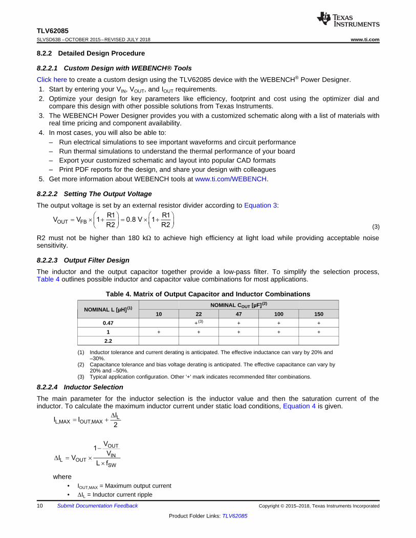
8.2.2 Detailed Design Procedure
8.2.2.1 Custom Design with WEBENCH® ToolsClick here to create a custom design using the TLV62085 device with the WEBENCH® Power Designer.1. Start by entering your VIN, VOUT, and IOUT requirements.2. Optimize your design for key parameters like efficiency, footprint and cost using the optimizer dial and
compare this design with other possible solutions from Texas Instruments.3. The WEBENCH Power Designer provides you with a customized schematic along with a list of materials with
real time pricing and component availability.4. In most cases, you will also be able to:
– Run electrical simulations to see important waveforms and circuit performance– Run thermal simulations to understand the thermal performance of your board– Export your customized schematic and layout into popular CAD formats– Print PDF reports for the design, and share your design with colleagues
5. Get more information about WEBENCH tools at www.ti.com/WEBENCH.
8.2.2.2 Setting The Output VoltageThe output voltage is set by an external resistor divider according to Equation 3:
(3)
R2 must not be higher than 180 kΩ to achieve high efficiency at light load while providing acceptable noisesensitivity.
8.2.2.3 Output Filter DesignThe inductor and the output capacitor together provide a low-pass filter. To simplify the selection process,Table 4 outlines possible inductor and capacitor value combinations for most applications.
(1) Inductor tolerance and current derating is anticipated. The effective inductance can vary by 20% and–30%.
(2) Capacitance tolerance and bias voltage derating is anticipated. The effective capacitance can vary by20% and –50%.
(3) Typical application configuration. Other '+' mark indicates recommended filter combinations.
Table 4. Matrix of Output Capacitor and Inductor Combinations
NOMINAL L [µH] (1) NOMINAL COUT [µF] (2)
10 22 47 100 1500.47 + (3) + + +
1 + + + + +2.2
8.2.2.4 Inductor SelectionThe main parameter for the inductor selection is the inductor value and then the saturation current of theinductor. To calculate the maximum inductor current under static load conditions, Equation 4 is given.
where• IOUT,MAX = Maximum output current• ΔIL = Inductor current ripple

11
TLV62085www.ti.com SLVSD63B –OCTOBER 2015–REVISED JULY 2018
Product Folder Links: TLV62085
Submit Documentation FeedbackCopyright © 2015–2018, Texas Instruments Incorporated
(1) See Third-Party Products disclaimer.
• fSW = Switching frequency• L = Inductor value (4)
TI recommends choosing the saturation current for the inductor 20% to 30% higher than the IL,MAX, out ofEquation 4. A higher inductor value is also useful to lower ripple current but increases the transient responsetime as well. The following inductors are recommended to be used in designs.
Table 5. List of Recommended Inductors (1)
INDUCTANCE[µH]
CURRENT RATING[A]
DIMENSIONSL × W × H [mm3]
DC RESISTANCE[mΩ typical] PART NUMBER
0.47 6.6 4 × 4 × 1.5 7.6 Coilcraft XFL4015-4710.47 4.7 3.2 × 2.5 × 1.2 21 TOKO DFE322512-R47N
1 5.1 4 × 4 × 2 10.8 Coilcraft XFL4020-102
8.2.2.5 Capacitor SelectionThe input capacitor is the low-impedance energy source for the converter which helps to provide stableoperation. A low ESR multilayer ceramic capacitor is recommended for best filtering and must be placed betweenVIN and GND as close as possible to those pins. For most applications, 10 μF is sufficient, though a larger valuereduces input current ripple.
The architecture of the TLV62085 allows the use of tiny ceramic output capacitors with low equivalent seriesresistance (ESR). These capacitors provide low output voltage ripple and are recommended. To keep its lowresistance up to high frequencies and to get narrow capacitance variation with temperature, TI recommendsusing X7R or X5R dielectrics. The recommended typical output capacitor value is 22 μF; this capacitance canvary over a wide range as outline in the output filter selection table. Output capacitors above 150uF may be usedwith a reduced load current during startup to avoid triggering the short circuit protection.
A feed-forward capacitor is not required for device proper operation.

Input Voltage (V)
Out
put V
olta
ge (
V)
2.5 3.0 3.5 4.0 4.5 5.0 5.5 6.01.188
1.194
1.200
1.206
1.212
D005
TA = -40°CTA = 25°CTA = 85°C
Load (A)
Out
put V
olta
ge (
V)
1.188
1.194
1.200
1.206
1.212
1m 10m 100m 1 5
D006
TA = -40°CTA = 25°CTA = 85°C
Load (A)
Effi
cien
cy (
%)
60
70
80
90
100
1m 10m 100m 1 5D003
VIN = 3.6 VVIN = 4.2 VVIN = 5.0 V
Load (A)
Effi
cien
cy (
%)
60
70
80
90
100
1m 10m 100m 1 5D004
VIN = 2.5 VVIN = 3.3 VVIN = 4.2 VVIN = 5.0 V
Load (A)
Effi
cien
cy (
%)
60
70
80
90
100
1m 10m 100m 1 5D001
VIN = 2.5 VVIN = 3.3 VVIN = 4.2 VVIN = 5.0 V
Load (A)
Effi
cien
cy (
%)
60
70
80
90
100
1m 10m 100m 1 5D002
VIN = 2.5 VVIN = 3.3 VVIN = 4.2 VVIN = 5.0 V
12
TLV62085SLVSD63B –OCTOBER 2015–REVISED JULY 2018 www.ti.com
Product Folder Links: TLV62085
Submit Documentation Feedback Copyright © 2015–2018, Texas Instruments Incorporated
8.2.3 Application CurvesVIN = 3.6 V, TA = 25 ºC, unless otherwise noted
VOUT = 0.95 V
Figure 5. Efficiency
VOUT = 1.2 V
Figure 6. Efficiency
VOUT = 3.3 V
Figure 7. Efficiency
VOUT = 1.8 V
Figure 8. Efficiency
IOUT = 1 A
Figure 9. Line Regulation Figure 10. Load Regulation

EN (DC, 5V/div)
Vout (DC, 0.5V/div)
Icoil (DC, 0.5A/div)
t -- 200 s/divμ
PG (DC, 5V/div)
EN (DC, 5V/div)
Vout (DC, 0.5V/div)
Icoil (DC, 2A/div)
t -- 5 s/divμ
PG (DC, 5V/div)
Load (DC, 2A/div)
Vout (AC, 50mV/div)
Icoil (DC, 2A/div)
t -- 200 s/divμ
EN (DC, 5V/div)
Vout (DC, 0.5V/div)
Icoil (DC, 2A/div)
t -- 200 s/divμ
PG (DC, 5V/div)
Vout (AC, 20mV/div)
Icoil (DC, 1A/div)
SW (DC, 5V/div)
t -- 300ns/div
Vout (AC, 20mV/div)
Icoil (DC, 1A/div)
SW (DC, 5V/div)
t -- 500ns/div
13
TLV62085www.ti.com SLVSD63B –OCTOBER 2015–REVISED JULY 2018
Product Folder Links: TLV62085
Submit Documentation FeedbackCopyright © 2015–2018, Texas Instruments Incorporated
IOUT = 3 A VOUT = 1.2 V
Figure 11. PWM Operation
IOUT = 0.1 A VOUT = 1.2 V
Figure 12. PFM Operation
IOUT = 0 A to 3 A VOUT = 1.2 V
Figure 13. Load Sweep
ROUT = 0.47 Ω VOUT = 1.2 V
Figure 14. Start-Up with Load
VOUT = 1.2 V
Figure 15. Start-Up without Load
ROUT = 0.47 Ω VOUT = 1.2 V
Figure 16. Shutdown with Load

Vout (DC, 0.5V/div)
Icoil (DC, 2A/div)
t -- 200 s/divμ
PG (DC, 5V/div)
Vout (DC, 0.5V/div)
Icoil (DC, 2A/div)
t -- 5 s/divμ
PG (DC, 5V/div)
Load (DC, 2A/div)
Vout (DC, 0.1V/div)
Icoil (DC, 2A/div)
t -- 3 s/divμ
PG (DC, 5V/div)Vout (DC, 0.5V/div)
Icoil (DC, 2A/div)
t -- 200 s/divμ
PG (DC, 5V/div)
EN (DC, 5V/div)
Vout (DC, 0.5V/div)
Icoil (DC, 0.5A/div)
t -- 5ms/div
PG (DC, 5V/div)
Load (DC, 2A/div)
Vout (DC, 0.1V/div)
Icoil (DC, 2A/div)
t -- 2 s/divμ
PG (DC, 5V/div)
14
TLV62085SLVSD63B –OCTOBER 2015–REVISED JULY 2018 www.ti.com
Product Folder Links: TLV62085
Submit Documentation Feedback Copyright © 2015–2018, Texas Instruments Incorporated
VOUT = 1.2 V
Figure 17. Shutdown without Load
IOUT = 0.5 A to 3 A VOUT = 1.2 V
Figure 18. Load Transient
IOUT = 50mA to 3A VOUT = 1.2 V
Figure 19. Load Transient
ROUT = 0.47 Ω VOUT = 1.2 V
Figure 20. Output Short-Circuit Protection, Entry
ROUT = 0.47 Ω VOUT = 1.2 V
Figure 21. Output Short-Circuit Protection, Recovery
ROUT = 0.47 Ω VOUT = 1.2 V
Figure 22. Output Short-Circuit Protection,HICCUP Zoom In

L1
C1C2
R1
R2
VIN
GND
VOUT
Solution Size
62 mm2 V
IN
SW
GN
D
EN
PG
FB
VO
S
15
TLV62085www.ti.com SLVSD63B –OCTOBER 2015–REVISED JULY 2018
Product Folder Links: TLV62085
Submit Documentation FeedbackCopyright © 2015–2018, Texas Instruments Incorporated
9 Power Supply RecommendationsThe device is designed to operate from an input voltage supply range from 2.5 V to 6 V. Ensure that the inputpower supply has a sufficient current rating for the application.
10 Layout
10.1 Layout GuidelinesThe printed-circuit-board (PCB) layout is an important step to maintain the high performance of the TLV62085device.
The input and output capacitors and the inductor must be placed as close as possible to the IC. This keeps thetraces short. Routing these traces direct and wide results in low trace resistance and low parasitic inductance.The low side of the input and output capacitors must be connected directly to the GND pin to avoid a groundpotential shift. The sense traces connected to FB and VOS pins are signal traces. Special care must be taken toavoid noise being induced. By a direct routing, parasitic inductance can be kept small. GND layers might be usedfor shielding. Keep these traces away from SW nodes. See Figure 23 for the recommended PCB layout.
10.2 Layout Example
Figure 23. PCB Layout Recommendation
10.3 Thermal ConsiderationsImplementation of integrated circuits in low-profile and fine-pitch surface-mount packages typically requiresspecial attention to power dissipation. Many system-dependent issues such as thermal coupling, airflow, addedheat sinks and convection surfaces, and the presence of other heat-generating components affect the powerdissipation limits of a given component.
Two basic approaches for enhancing thermal performance are:• Improving the power dissipation capability of the PCB design• Introducing airflow in the system
The big copper planes connecting to the pads of the IC on the PCB improve the thermal performance of thedevice. For more details on how to use the thermal parameters, see the Thermal Characteristics ApplicationNotes, SZZA017 and SPRA953.

16
TLV62085SLVSD63B –OCTOBER 2015–REVISED JULY 2018 www.ti.com
Product Folder Links: TLV62085
Submit Documentation Feedback Copyright © 2015–2018, Texas Instruments Incorporated
11 Device and Documentation Support
11.1 Development Support
11.1.1 Custom Design with WEBENCH® ToolsClick here to create a custom design using the TLV62085 device with the WEBENCH® Power Designer.1. Start by entering your VIN, VOUT, and IOUT requirements.2. Optimize your design for key parameters like efficiency, footprint and cost using the optimizer dial and
compare this design with other possible solutions from Texas Instruments.3. The WEBENCH Power Designer provides you with a customized schematic along with a list of materials with
real time pricing and component availability.4. In most cases, you will also be able to:
– Run electrical simulations to see important waveforms and circuit performance– Run thermal simulations to understand the thermal performance of your board– Export your customized schematic and layout into popular CAD formats– Print PDF reports for the design, and share your design with colleagues
5. Get more information about WEBENCH tools at www.ti.com/WEBENCH.
11.1.2 Third-Party Products DisclaimerTI'S PUBLICATION OF INFORMATION REGARDING THIRD-PARTY PRODUCTS OR SERVICES DOES NOTCONSTITUTE AN ENDORSEMENT REGARDING THE SUITABILITY OF SUCH PRODUCTS OR SERVICESOR A WARRANTY, REPRESENTATION OR ENDORSEMENT OF SUCH PRODUCTS OR SERVICES, EITHERALONE OR IN COMBINATION WITH ANY TI PRODUCT OR SERVICE.
11.2 Documentation Support
11.2.1 Related DocumentationFor related documentation, see the following:• Thermal Characteristics Application Note, SZZA017• Thermal Characteristics Application Note, SPRA953
11.3 Receiving Notification of Documentation UpdatesTo receive notification of documentation updates, navigate to the device product folder on ti.com. In the upperright corner, click on Alert me to register and receive a weekly digest of any product information that haschanged. For change details, review the revision history included in any revised document.
11.4 Community ResourcesThe following links connect to TI community resources. Linked contents are provided "AS IS" by the respectivecontributors. They do not constitute TI specifications and do not necessarily reflect TI's views; see TI's Terms ofUse.
TI E2E™ Online Community TI's Engineer-to-Engineer (E2E) Community. Created to foster collaborationamong engineers. At e2e.ti.com, you can ask questions, share knowledge, explore ideas and helpsolve problems with fellow engineers.
Design Support TI's Design Support Quickly find helpful E2E forums along with design support tools andcontact information for technical support.
11.5 TrademarksDCS-Control, WEBENCH, E2E are trademarks of Texas Instruments.WEBENCH is a registered trademark of Texas Instruments.

17
TLV62085www.ti.com SLVSD63B –OCTOBER 2015–REVISED JULY 2018
Product Folder Links: TLV62085
Submit Documentation FeedbackCopyright © 2015–2018, Texas Instruments Incorporated
11.6 Electrostatic Discharge CautionThese devices have limited built-in ESD protection. The leads should be shorted together or the device placed in conductive foamduring storage or handling to prevent electrostatic damage to the MOS gates.
11.7 GlossarySLYZ022 — TI Glossary.
This glossary lists and explains terms, acronyms, and definitions.
12 Mechanical, Packaging, and Orderable InformationThe following pages include mechanical, packaging, and orderable information. This information is the mostcurrent data available for the designated devices. This data is subject to change without notice and revision ofthis document. For browser-based versions of this data sheet, refer to the left-hand navigation.

PACKAGE OPTION ADDENDUM
www.ti.com 16-Jul-2018
Addendum-Page 1
PACKAGING INFORMATION
Orderable Device Status(1)
Package Type PackageDrawing
Pins PackageQty
Eco Plan(2)
Lead/Ball Finish(6)
MSL Peak Temp(3)
Op Temp (°C) Device Marking(4/5)
Samples
TLV62085RLTR ACTIVE VSON-HR RLT 7 3000 Green (RoHS& no Sb/Br)
CU NIPDAU Level-1-260C-UNLIM -40 to 125 12Q5
TLV62085RLTT ACTIVE VSON-HR RLT 7 250 Green (RoHS& no Sb/Br)
CU NIPDAU Level-1-260C-UNLIM -40 to 125 12Q5
(1) The marketing status values are defined as follows:ACTIVE: Product device recommended for new designs.LIFEBUY: TI has announced that the device will be discontinued, and a lifetime-buy period is in effect.NRND: Not recommended for new designs. Device is in production to support existing customers, but TI does not recommend using this part in a new design.PREVIEW: Device has been announced but is not in production. Samples may or may not be available.OBSOLETE: TI has discontinued the production of the device.
(2) RoHS: TI defines "RoHS" to mean semiconductor products that are compliant with the current EU RoHS requirements for all 10 RoHS substances, including the requirement that RoHS substancedo not exceed 0.1% by weight in homogeneous materials. Where designed to be soldered at high temperatures, "RoHS" products are suitable for use in specified lead-free processes. TI mayreference these types of products as "Pb-Free".RoHS Exempt: TI defines "RoHS Exempt" to mean products that contain lead but are compliant with EU RoHS pursuant to a specific EU RoHS exemption.Green: TI defines "Green" to mean the content of Chlorine (Cl) and Bromine (Br) based flame retardants meet JS709B low halogen requirements of <=1000ppm threshold. Antimony trioxide basedflame retardants must also meet the <=1000ppm threshold requirement.
(3) MSL, Peak Temp. - The Moisture Sensitivity Level rating according to the JEDEC industry standard classifications, and peak solder temperature.
(4) There may be additional marking, which relates to the logo, the lot trace code information, or the environmental category on the device.
(5) Multiple Device Markings will be inside parentheses. Only one Device Marking contained in parentheses and separated by a "~" will appear on a device. If a line is indented then it is a continuationof the previous line and the two combined represent the entire Device Marking for that device.
(6) Lead/Ball Finish - Orderable Devices may have multiple material finish options. Finish options are separated by a vertical ruled line. Lead/Ball Finish values may wrap to two lines if the finishvalue exceeds the maximum column width.
Important Information and Disclaimer:The information provided on this page represents TI's knowledge and belief as of the date that it is provided. TI bases its knowledge and belief on informationprovided by third parties, and makes no representation or warranty as to the accuracy of such information. Efforts are underway to better integrate information from third parties. TI has taken andcontinues to take reasonable steps to provide representative and accurate information but may not have conducted destructive testing or chemical analysis on incoming materials and chemicals.TI and TI suppliers consider certain information to be proprietary, and thus CAS numbers and other limited information may not be available for release.
In no event shall TI's liability arising out of such information exceed the total purchase price of the TI part(s) at issue in this document sold by TI to Customer on an annual basis.

PACKAGE OPTION ADDENDUM
www.ti.com 16-Jul-2018
Addendum-Page 2

TAPE AND REEL INFORMATION
*All dimensions are nominal
Device PackageType
PackageDrawing
Pins SPQ ReelDiameter
(mm)
ReelWidth
W1 (mm)
A0(mm)
B0(mm)
K0(mm)
P1(mm)
W(mm)
Pin1Quadrant
TLV62085RLTR VSON-HR
RLT 7 3000 180.0 8.4 2.3 2.3 1.15 4.0 8.0 Q2
TLV62085RLTT VSON-HR
RLT 7 250 180.0 8.4 2.3 2.3 1.15 4.0 8.0 Q2
PACKAGE MATERIALS INFORMATION
www.ti.com 16-Jul-2018
Pack Materials-Page 1

*All dimensions are nominal
Device Package Type Package Drawing Pins SPQ Length (mm) Width (mm) Height (mm)
TLV62085RLTR VSON-HR RLT 7 3000 210.0 185.0 35.0
TLV62085RLTT VSON-HR RLT 7 250 210.0 185.0 35.0
PACKAGE MATERIALS INFORMATION
www.ti.com 16-Jul-2018
Pack Materials-Page 2

NOTES:
1. All linear dimensions are in millimeters. Any dimensions in parenthesis are for reference only. Dimensioning and tolerancing
per ASME Y14.5M.
2. This drawing is subject to change without notice.
PACKAGE OUTLINE
www.ti.com
4220429/A 09/2014
VSON - 1 mm max height
PLASTIC SMALL OUTLINE - NO LEAD
RLT0007A
2.1
1.9
2.1
1.9
(0.2) TYP
B
A
SEATING PLANE
C
1 MAX
0.05
0.00
0.08
PIN 1
INDEX AREA
2X 0.6
3X
0.35
0.25
0.1 C A B
0.05 C
3X
1.4
1.2
1.5
PIN 1 ID
1
4
7
5
3X
0.5
0.3
1.2
4X
0.3
0.2
0.1 C A B
0.05 C
3X 0.5
1
0.5
0.3
(0.2) TYP

NOTES: (continued)
3. For more information, see Texas Instruments literature number SLUA271 (www.ti.com/lit/slua271).
4. Solder mask tolerances between and around signal pads can vary based on board fabrication site.
5. Vias should not be placed on soldering pads unless they are plugged or plated shut.
EXAMPLE BOARD LAYOUT
4220429/A 09/2014
www.ti.com
VSON - 1 mm max height
RLT0007A
PLASTIC SMALL OUTLINE - NO LEAD
PKG
PKG
3X (0.6)
3X (0.25)
(0.6)
(0.25)
3X (1.5)
3X (0.3)
2X (0.6)
3X (0.5)
(0.45)(0.9)
1
4
5
7
NON SOLDER MASK
DEFINED
PADS 1 - 4
SOLDER MASK
DEFINED
PADS 5 - 7
SOLDER MASK DETAILS
0.07 MAX
ALL AROUND
0.07 MIN
ALL AROUND
SOLDER MASK
OPENING
METAL UNDER
SOLDER MASK
METAL
SOLDER MASK
OPENING
LAND PATTERN EXAMPLE
SCALE: 30X

NOTES: (continued)
6. Laser cutting apertures with trapezoidal walls and rounded corners may offer better paste release. IPC-7525 may have alternate
design recommendations.
EXAMPLE STENCIL DESIGN
4220429/A 09/2014
www.ti.com
VSON - 1 mm max height
RLT0007A
PLASTIC SMALL OUTLINE - NO LEAD
SOLDER PASTE EXAMPLE
BASED ON 0.125 mm THICK STENCIL
FOR ALL EXPOSED PADS
85% PRINTED SOLDER COVERAGE BY AREA
SCALE: 40X
PKG
PKG
3X (0.6)
3X (0.21)
(0.6)
(0.21)
6X (0.65)
6X (0.3)
2X (0.6)
3X (0.5)
3X (0.025)
(0.9)
1
4
5
7
3X
EXPOSED METAL
METAL UNDER
SOLDER MASK
TYP
(0.875)
EXPOSED METAL
TYP
SOLDER MASK EDGE
TYP

IMPORTANT NOTICE
Texas Instruments Incorporated (TI) reserves the right to make corrections, enhancements, improvements and other changes to itssemiconductor products and services per JESD46, latest issue, and to discontinue any product or service per JESD48, latest issue. Buyersshould obtain the latest relevant information before placing orders and should verify that such information is current and complete.TI’s published terms of sale for semiconductor products (http://www.ti.com/sc/docs/stdterms.htm) apply to the sale of packaged integratedcircuit products that TI has qualified and released to market. Additional terms may apply to the use or sale of other types of TI products andservices.Reproduction of significant portions of TI information in TI data sheets is permissible only if reproduction is without alteration and isaccompanied by all associated warranties, conditions, limitations, and notices. TI is not responsible or liable for such reproduceddocumentation. Information of third parties may be subject to additional restrictions. Resale of TI products or services with statementsdifferent from or beyond the parameters stated by TI for that product or service voids all express and any implied warranties for theassociated TI product or service and is an unfair and deceptive business practice. TI is not responsible or liable for any such statements.Buyers and others who are developing systems that incorporate TI products (collectively, “Designers”) understand and agree that Designersremain responsible for using their independent analysis, evaluation and judgment in designing their applications and that Designers havefull and exclusive responsibility to assure the safety of Designers' applications and compliance of their applications (and of all TI productsused in or for Designers’ applications) with all applicable regulations, laws and other applicable requirements. Designer represents that, withrespect to their applications, Designer has all the necessary expertise to create and implement safeguards that (1) anticipate dangerousconsequences of failures, (2) monitor failures and their consequences, and (3) lessen the likelihood of failures that might cause harm andtake appropriate actions. Designer agrees that prior to using or distributing any applications that include TI products, Designer willthoroughly test such applications and the functionality of such TI products as used in such applications.TI’s provision of technical, application or other design advice, quality characterization, reliability data or other services or information,including, but not limited to, reference designs and materials relating to evaluation modules, (collectively, “TI Resources”) are intended toassist designers who are developing applications that incorporate TI products; by downloading, accessing or using TI Resources in anyway, Designer (individually or, if Designer is acting on behalf of a company, Designer’s company) agrees to use any particular TI Resourcesolely for this purpose and subject to the terms of this Notice.TI’s provision of TI Resources does not expand or otherwise alter TI’s applicable published warranties or warranty disclaimers for TIproducts, and no additional obligations or liabilities arise from TI providing such TI Resources. TI reserves the right to make corrections,enhancements, improvements and other changes to its TI Resources. TI has not conducted any testing other than that specificallydescribed in the published documentation for a particular TI Resource.Designer is authorized to use, copy and modify any individual TI Resource only in connection with the development of applications thatinclude the TI product(s) identified in such TI Resource. NO OTHER LICENSE, EXPRESS OR IMPLIED, BY ESTOPPEL OR OTHERWISETO ANY OTHER TI INTELLECTUAL PROPERTY RIGHT, AND NO LICENSE TO ANY TECHNOLOGY OR INTELLECTUAL PROPERTYRIGHT OF TI OR ANY THIRD PARTY IS GRANTED HEREIN, including but not limited to any patent right, copyright, mask work right, orother intellectual property right relating to any combination, machine, or process in which TI products or services are used. Informationregarding or referencing third-party products or services does not constitute a license to use such products or services, or a warranty orendorsement thereof. Use of TI Resources may require a license from a third party under the patents or other intellectual property of thethird party, or a license from TI under the patents or other intellectual property of TI.TI RESOURCES ARE PROVIDED “AS IS” AND WITH ALL FAULTS. TI DISCLAIMS ALL OTHER WARRANTIES ORREPRESENTATIONS, EXPRESS OR IMPLIED, REGARDING RESOURCES OR USE THEREOF, INCLUDING BUT NOT LIMITED TOACCURACY OR COMPLETENESS, TITLE, ANY EPIDEMIC FAILURE WARRANTY AND ANY IMPLIED WARRANTIES OFMERCHANTABILITY, FITNESS FOR A PARTICULAR PURPOSE, AND NON-INFRINGEMENT OF ANY THIRD PARTY INTELLECTUALPROPERTY RIGHTS. TI SHALL NOT BE LIABLE FOR AND SHALL NOT DEFEND OR INDEMNIFY DESIGNER AGAINST ANY CLAIM,INCLUDING BUT NOT LIMITED TO ANY INFRINGEMENT CLAIM THAT RELATES TO OR IS BASED ON ANY COMBINATION OFPRODUCTS EVEN IF DESCRIBED IN TI RESOURCES OR OTHERWISE. IN NO EVENT SHALL TI BE LIABLE FOR ANY ACTUAL,DIRECT, SPECIAL, COLLATERAL, INDIRECT, PUNITIVE, INCIDENTAL, CONSEQUENTIAL OR EXEMPLARY DAMAGES INCONNECTION WITH OR ARISING OUT OF TI RESOURCES OR USE THEREOF, AND REGARDLESS OF WHETHER TI HAS BEENADVISED OF THE POSSIBILITY OF SUCH DAMAGES.Unless TI has explicitly designated an individual product as meeting the requirements of a particular industry standard (e.g., ISO/TS 16949and ISO 26262), TI is not responsible for any failure to meet such industry standard requirements.Where TI specifically promotes products as facilitating functional safety or as compliant with industry functional safety standards, suchproducts are intended to help enable customers to design and create their own applications that meet applicable functional safety standardsand requirements. Using products in an application does not by itself establish any safety features in the application. Designers mustensure compliance with safety-related requirements and standards applicable to their applications. Designer may not use any TI products inlife-critical medical equipment unless authorized officers of the parties have executed a special contract specifically governing such use.Life-critical medical equipment is medical equipment where failure of such equipment would cause serious bodily injury or death (e.g., lifesupport, pacemakers, defibrillators, heart pumps, neurostimulators, and implantables). Such equipment includes, without limitation, allmedical devices identified by the U.S. Food and Drug Administration as Class III devices and equivalent classifications outside the U.S.TI may expressly designate certain products as completing a particular qualification (e.g., Q100, Military Grade, or Enhanced Product).Designers agree that it has the necessary expertise to select the product with the appropriate qualification designation for their applicationsand that proper product selection is at Designers’ own risk. Designers are solely responsible for compliance with all legal and regulatoryrequirements in connection with such selection.Designer will fully indemnify TI and its representatives against any damages, costs, losses, and/or liabilities arising out of Designer’s non-compliance with the terms and provisions of this Notice.
Mailing Address: Texas Instruments, Post Office Box 655303, Dallas, Texas 75265Copyright © 2018, Texas Instruments Incorporated