Embed Size (px)
Citation preview

Load (A)
Effi
cien
cy (
%)
50
60
70
80
90
100
1m 10m 100m 1 5
D017
VOUT = 1.0 VVOUT = 1.8 VVOUT = 2.5 VVOUT = 3.3 V
TPS82130
12 VR1124kΩ
R2100kΩ
VIN
POWER GOOD
VIN
EN
C222µF
R3100kΩ
VOUT
1.8 V/3 AC110µF
SS/TR
GNDPG
FB
VOUT
C33.3nF
Copyright © 2016, Texas Instruments Incorporated
Product
Folder
Order
Now
Technical
Documents
Tools &
Software
Support &Community
An IMPORTANT NOTICE at the end of this data sheet addresses availability, warranty, changes, use in safety-critical applications,intellectual property matters and other important disclaimers. PRODUCTION DATA.
TPS82130SLVSCY5C –FEBRUARY 2016–REVISED JANUARY 2017
TPS82130 17-V Input 3-A Step-Down Converter MicroSiP™ Module with IntegratedInductor
1
1 Features1• 3.0-mm x 2.8-mm x 1.5-mm MicroSiP™ Package• 3.0-V to 17-V Input Range• 3-A Continuous Output Current• DCS-Control™ Topology• Power Save Mode for Light Load Efficiency• 20-µA Operating Quiescent Current• 0.9-V to 6-V Adjustable Output Voltage• 100% Duty Cycle for Lowest Dropout• Power Good Output• Programmable Soft Startup with Tracking• Thermal Shutdown Protection• –40°C to 125°C Operating Temperature Range• Create a Custom Design using the TPS82130 with
the WEBENCH® Power Designer
2 Applications• Industrial Applications• Telecom and Networking Applications• Solid State Drives
3 DescriptionThe TPS82130 is a 17-V input 3-A step-downconverter MicroSiP™ power module optimized forsmall solution size and high efficiency. The moduleintegrates a synchronous step-down converter and aninductor to simplify design, reduce externalcomponents and save PCB area. The low profile andcompact solution is suitable for automated assemblyby standard surface mount equipment.
To maximize efficiency, the converter operates inPWM mode with a nominal switching frequency of2 MHz and automatically enters Power Save Modeoperation at light load currents. In Power Save Mode,the device operates with typically 20-µA quiescentcurrent. Using the DCS-Control™ topology, thedevice achieves excellent load transient performanceand accurate output voltage regulation.
Device Information(1)
PART NUMBER PACKAGE BODY SIZE (NOM)TPS82130SIL µSiL (8) 3.0 mm x 2.8 mm x 1.5 mm
(1) For all available packages, see the orderable addendum atthe end of the data sheet.
SPACER
Simplified Schematic1.8-V Output Application 12-V Input Voltage Efficiency

2
TPS82130SLVSCY5C –FEBRUARY 2016–REVISED JANUARY 2017 www.ti.com
Product Folder Links: TPS82130
Submit Documentation Feedback Copyright © 2016–2017, Texas Instruments Incorporated
Table of Contents1 Features .................................................................. 12 Applications ........................................................... 13 Description ............................................................. 14 Revision History..................................................... 25 Pin Configuration and Functions ......................... 36 Specifications......................................................... 4
6.1 Absolute Maximum Ratings ...................................... 46.2 ESD Ratings.............................................................. 46.3 Recommend Operating Conditions........................... 46.4 Thermal Information .................................................. 46.5 Electrical Characteristics.......................................... 56.6 Typical Characteristics .............................................. 6
7 Detailed Description .............................................. 77.1 Overview ................................................................... 77.2 Functional Block Diagram ......................................... 77.3 Feature Description................................................... 77.4 Device Functional Modes.......................................... 9
8 Application and Implementation ........................ 118.1 Application Information............................................ 118.2 Typical Applications ................................................ 11
9 Power Supply Recommendations ...................... 1710 Layout................................................................... 17
10.1 Layout Guidelines ................................................. 1710.2 Layout Example .................................................... 1710.3 Thermal Consideration.......................................... 17
11 Device and Documentation Support ................. 1811.1 Development Support ........................................... 1811.2 Receiving Notification of Documentation Updates 1811.3 Community Resources.......................................... 1811.4 Trademarks ........................................................... 1811.5 Electrostatic Discharge Caution............................ 1811.6 Glossary ................................................................ 18
12 Mechanical, Packaging, and OrderableInformation ........................................................... 18
4 Revision HistoryNOTE: Page numbers for previous revisions may differ from page numbers in the current version.
Changes from Revision B (August 2016) to Revision C Page
• Added WEBENCH information to the Features, Detailed Design Procedure, and Device Support sections ....................... 1• Changed the Output voltage MAX value From: 5 V to: 6 V in the Recommend Operating Conditions table ........................ 4• Added Table 1, Power Good Pin Logic ................................................................................................................................ 10
Changes from Revision A (February 2015) to Revision B Page
• Changed storage temperature to -55°C from -40°C............................................................................................................... 4• Updated thermal information .................................................................................................................................................. 4• Added FB voltage accuracy at TJ = 0°C to 85°C condition .................................................................................................... 5• Changed derating curve based on ambient temperature .................................................................................................... 13• Changed derating curve based on ambient temperature ..................................................................................................... 13• Added derating curve for VOUT = 1.0 V................................................................................................................................. 14• Deleted Thermal pictures ..................................................................................................................................................... 17• Added "Receiving Notification of Documentation Updates" section..................................................................................... 18
Changes from Original (December 2015) to Revision A Page
• Production Data release ........................................................................................................................................................ 1

1
2
3
4
8
7
6
5
EX
PO
SE
D
TH
ER
MA
LPA
D
EN
VIN
GND
VOUT
SS/TR
FB
PG
VOUT
3
TPS82130www.ti.com SLVSCY5C –FEBRUARY 2016–REVISED JANUARY 2017
Product Folder Links: TPS82130
Submit Documentation FeedbackCopyright © 2016–2017, Texas Instruments Incorporated
5 Pin Configuration and Functions
space
8-Pin µSiL Package(SIL0008C Top View)
space
Pin FunctionsPIN
I/O DESCRIPTIONNAME NO.
EN 1 I Enable pin. Pull High to enable the device. Pull Low to disable the device. This pin has aninternal pull-down resistor of typically 400kΩ when the device is disabled.
VIN 2 PWR Input pin.GND 3 Ground pin.VOUT 4,5 PWR Output pin.
FB 6 I Feedback reference pin. An external resistor divider connected to this pin programs the outputvoltage.
PG 7 O Power good open drain output pin. A pull-up resistor can be connected to any voltage less than6V. Leave it open if it is not used.
SS/TR 8 I Soft startup and voltage tracking pin. An external capacitor connected to this pin sets the internalreference voltage rising time.
Exposed Thermal Pad The exposed thermal pad must be connected to the GND pin. Must be soldered to achieveappropriate power dissipation and mechanical reliability.
4
TPS82130SLVSCY5C –FEBRUARY 2016–REVISED JANUARY 2017 www.ti.com
Product Folder Links: TPS82130
Submit Documentation Feedback Copyright © 2016–2017, Texas Instruments Incorporated
(1) Stresses beyond those listed under absolute maximum ratings may cause permanent damage to the device. These are stress ratingsonly, and functional operation of the device at these or any other conditions beyond those indicated under recommended operatingconditions is not implied. Exposure to absolute-maximum-rated conditions for extended periods may affect device reliability.
(2) All voltage values are with respect to network ground pin.
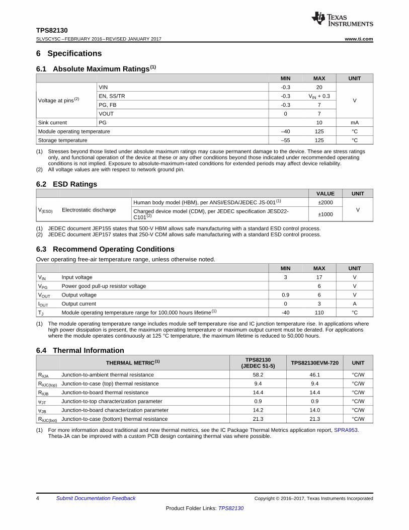
6 Specifications
6.1 Absolute Maximum Ratings (1)
MIN MAX UNIT
Voltage at pins (2)
VIN -0.3 20
VEN, SS/TR -0.3 VIN + 0.3PG, FB -0.3 7VOUT 0 7
Sink current PG 10 mAModule operating temperature –40 125 °CStorage temperature –55 125 °C
(1) JEDEC document JEP155 states that 500-V HBM allows safe manufacturing with a standard ESD control process.(2) JEDEC document JEP157 states that 250-V CDM allows safe manufacturing with a standard ESD control process.
6.2 ESD RatingsVALUE UNIT
V(ESD) Electrostatic dischargeHuman body model (HBM), per ANSI/ESDA/JEDEC JS-001 (1) ±2000
VCharged device model (CDM), per JEDEC specification JESD22-C101 (2) ±1000
(1) The module operating temperature range includes module self temperature rise and IC junction temperature rise. In applications wherehigh power dissipation is present, the maximum operating temperature or maximum output current must be derated. For applicationswhere the module operates continuously at 125 °C temperature, the maximum lifetime is reduced to 50,000 hours.
6.3 Recommend Operating ConditionsOver operating free-air temperature range, unless otherwise noted.
MIN MAX UNITVIN Input voltage 3 17 VVPG Power good pull-up resistor voltage 6 VVOUT Output voltage 0.9 6 VIOUT Output current 0 3 ATJ Module operating temperature range for 100,000 hours lifetime (1) -40 110 °C
(1) For more information about traditional and new thermal metrics, see the IC Package Thermal Metrics application report, SPRA953.Theta-JA can be improved with a custom PCB design containing thermal vias where possible.
6.4 Thermal InformationTHERMAL METRIC (1) TPS82130
(JEDEC 51-5) TPS82130EVM-720 UNIT
RθJA Junction-to-ambient thermal resistance 58.2 46.1 °C/WRθJC(top) Junction-to-case (top) thermal resistance 9.4 9.4 °C/WRθJB Junction-to-board thermal resistance 14.4 14.4 °C/WψJT Junction-to-top characterization parameter 0.9 0.9 °C/WψJB Junction-to-board characterization parameter 14.2 14.0 °C/WRθJC(bot) Junction-to-case (bottom) thermal resistance 21.3 21.3 °C/W
5
TPS82130www.ti.com SLVSCY5C –FEBRUARY 2016–REVISED JANUARY 2017
Product Folder Links: TPS82130
Submit Documentation FeedbackCopyright © 2016–2017, Texas Instruments Incorporated
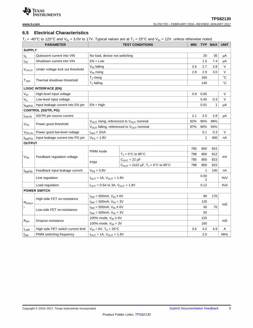
6.5 Electrical CharacteristicsTJ = -40°C to 125°C and VIN = 3.0V to 17V. Typical values are at TJ = 25°C and VIN = 12V, unless otherwise noted.
PARAMETER TEST CONDITIONS MIN TYP MAX UNITSUPPLYIQ Quiescent current into VIN No load, device not switching 20 35 µAISD Shutdown current into VIN EN = Low 1.5 7.4 µA
VUVLO Under voltage lock out thresholdVIN falling 2.6 2.7 2.8 VVIN rising 2.8 2.9 3.0 V
TJSD Thermal shutdown thresholdTJ rising 160 °CTJ falling 140 °C
LOGIC INTERFACE (EN)VIH High-level input voltage 0.9 0.65 VVIL Low-level input voltage 0.45 0.3 VIlkg(EN) Input leakage current into EN pin EN = High 0.01 1 µACONTROL (SS/TR, PG)ISS/TR SS/TR pin source current 2.1 2.5 2.8 µA
VPG Power good thresholdVOUT rising, referenced to VOUT nominal 92% 95% 99%VOUT falling, referenced to VOUT nominal 87% 90% 94%
VPG,OL Power good low-level voltage Isink = 2mA 0.1 0.3 VIlkg(PG) Input leakage current into PG pin VPG = 1.8V 1 400 nAOUTPUT
VFB Feedback regulation voltagePWM mode
785 800 815
mVTJ = 0°C to 85°C 788 800 812
PSMCOUT = 22 µF 785 800 823COUT = 2x22 µF, TJ = 0°C to 85°C 788 800 815
Ilkg(FB) Feedback input leakage current VFB = 0.8V 1 100 nA
Line regulation IOUT = 1A, VOUT = 1.8V 0.002 %/V
Load regulation IOUT = 0.5A to 3A, VOUT = 1.8V 0.12 %/APOWER SWITCH
RDS(on)
High-side FET on-resistanceISW = 500mA, VIN ≥ 6V 90 170
mΩISW = 500mA, VIN = 3V 120
Low-side FET on-resistanceISW = 500mA, VIN ≥ 6V 40 70ISW = 500mA, VIN = 3V 50
RDP Dropout resistance100% mode, VIN ≥ 6V 125
mΩ100% mode, VIN = 3V 160
ILIMF High-side FET switch current limit VIN = 6V, TA = 25°C 3.6 4.2 4.9 AfSW PWM switching frequency IOUT = 1A, VOUT = 1.8V 2.0 MHz

Input Voltage (V)
6KXWGRZQ&XUUHQW$
3 5 7 9 11 13 15 170
2
4
6
8
D026
TJ = -40°CTJ = 25°CTJ = 85°CTJ = 125°C
Module Temperature (°C)
'URSRXW5HVLVWDQFHP
-40 -20 0 20 40 60 80 100 12050
100
150
200
250
D014
VIN = 3.0 VVIN = 6.0 V
Input Voltage (V)
4XLHVFHQW&XUUHQW$
3 5 7 9 11 13 15 170
10
20
30
40
50
D025
TJ = -40°CTJ = 25°CTJ = 85°CTJ = 125°C
6
TPS82130SLVSCY5C –FEBRUARY 2016–REVISED JANUARY 2017 www.ti.com
Product Folder Links: TPS82130
Submit Documentation Feedback Copyright © 2016–2017, Texas Instruments Incorporated
6.6 Typical Characteristics
Figure 1. Dropout Resistance Figure 2. Quiescent Current
Figure 3. Shutdown Current
IN
OUTON
V
Vns500t ´=
VOUT
FB
GND
Direct Controland
CompensationTimer
ton
Comparator
Ramp
Error AmplifierDCS - Control
TM
MOSFET DriverControl Logic
High SideCurrent Sense
VIN
BandgapUndervoltage Lockout
Thermal ShutdownEN
PG
VFB
VREF
VREF
400kΩ(1)
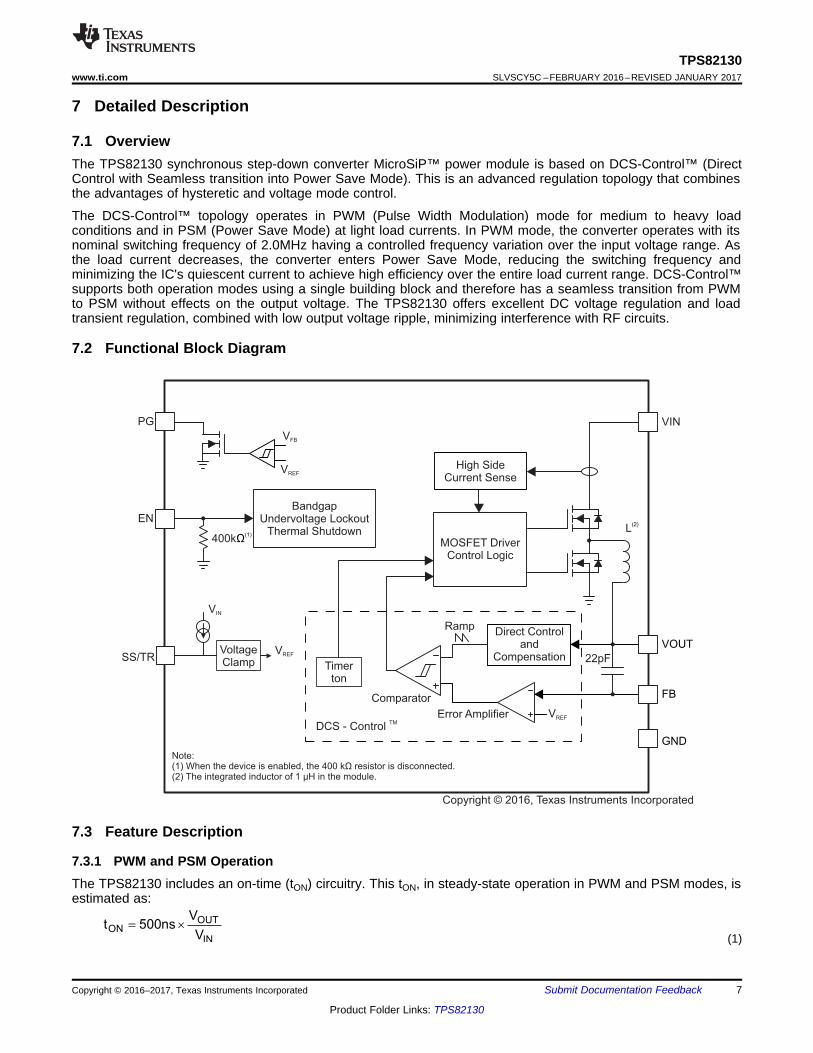
Note:(1) When the device is enabled, the 400 k resistor is disconnected.(2) The integrated inductor of 1 µH in the module.
Ω
L(2)
VoltageClamp
VIN
VREFSS/TR 22pF
Copyright © 2016, Texas Instruments Incorporated
7
TPS82130www.ti.com SLVSCY5C –FEBRUARY 2016–REVISED JANUARY 2017
Product Folder Links: TPS82130
Submit Documentation FeedbackCopyright © 2016–2017, Texas Instruments Incorporated
7 Detailed Description
7.1 OverviewThe TPS82130 synchronous step-down converter MicroSiP™ power module is based on DCS-Control™ (DirectControl with Seamless transition into Power Save Mode). This is an advanced regulation topology that combinesthe advantages of hysteretic and voltage mode control.
The DCS-Control™ topology operates in PWM (Pulse Width Modulation) mode for medium to heavy loadconditions and in PSM (Power Save Mode) at light load currents. In PWM mode, the converter operates with itsnominal switching frequency of 2.0MHz having a controlled frequency variation over the input voltage range. Asthe load current decreases, the converter enters Power Save Mode, reducing the switching frequency andminimizing the IC's quiescent current to achieve high efficiency over the entire load current range. DCS-Control™supports both operation modes using a single building block and therefore has a seamless transition from PWMto PSM without effects on the output voltage. The TPS82130 offers excellent DC voltage regulation and loadtransient regulation, combined with low output voltage ripple, minimizing interference with RF circuits.
7.2 Functional Block Diagram
7.3 Feature Description
7.3.1 PWM and PSM OperationThe TPS82130 includes an on-time (tON) circuitry. This tON, in steady-state operation in PWM and PSM modes, isestimated as:
(1)

DPOUT(min)OUT(min)IN RIVV ´+=
L
VV
V
Vt
I2f
OUTIN
OUT
IN2
ON
OUTPSM
-
´´
´
=
L
VVtI
OUTINONL
-´=D
8
TPS82130SLVSCY5C –FEBRUARY 2016–REVISED JANUARY 2017 www.ti.com
Product Folder Links: TPS82130
Submit Documentation Feedback Copyright © 2016–2017, Texas Instruments Incorporated
Feature Description (continued)In PWM mode, the TPS82130 operates with pulse width modulation in continuous conduction mode (CCM) witha tON shown in Equation 1 at medium and heavy load currents. A PWM switching frequency of typically 2.0MHzis achieved by this tON circuitry. The device operates in PWM mode as long as the output current is higher thanhalf the inductor's ripple current estimated by Equation 2.
(2)
To maintain high efficiency at light loads, the device enters Power Save Mode seamlessly when the load currentdecreases. This happens when the load current becomes smaller than half the inductor's ripple current. In PSM,the converter operates with reduced switching frequency and with a minimum quiescent current to maintain highefficiency. PSM is also based on the tON circuitry. The switching frequency in PSM is estimated as:
(3)
In PSM, the output voltage rises slightly above the nominal output voltage in PWM mode. This effect is reducedby increasing the output capacitance. The output voltage accuracy in PSM operation is reflected in the electricalspecification table and given for a 22-µF output capacitor.
For very small output voltages, an absolute minimum on-time of about 80ns is kept to limit switching losses. Theoperating frequency is thereby reduced from its nominal value, which keeps efficiency high. Also the off-time canreach its minimum value at high duty cycles. The output voltage remains regulated in such cases.
When VIN decreases to typically 15% above VOUT, the TPS82130 can't enter Power Save Mode, regardless ofthe load current. The device maintains output regulation in PWM mode.
7.3.2 Low Dropout Operation (100% Duty Cycle)The TPS82130 offers a low input to output voltage differential by entering 100% duty cycle mode. In this mode,the high-side MOSFET switch is constantly turned on. This is particularly useful in battery powered applicationsto achieve longest operation time by taking full advantage of the whole battery voltage range. The minimum inputvoltage to maintain a minimum output voltage is given by:
(4)
WhereRDP = Resistance from VIN to VOUT, including high-side FET on-resistance and DC resistance of the inductorVOUT(min) = Minimum output voltage the load can accept.
7.3.3 Switch Current LimitThe switch current limit prevents the device from high inductor current and from drawing excessive current fromthe battery or input voltage rail. Excessive current might occur with a heavy load/shorted output circuit condition.If the inductor peak current reaches the switch current limit after a propagation delay of typically 30 ns, the high-side FET is turned off and the low-side FET is turned on to ramp down the inductor current.
7.3.4 Undervoltage LockoutTo avoid mis-operation of the device at low input voltages, an under voltage lockout is implemented, which shutsdown the devices at voltages lower than VUVLO with a hysteresis of 200 mV.
7.3.5 Thermal ShutdownThe device goes into thermal shutdown and stops switching once the junction temperature exceeds TJSD. Oncethe device temperature falls below the threshold by 20°C, the device returns to normal operation automatically.
4R
4R3R
2R1R
2R64.0
V
V
1OUT
2OUT +´
+
´»
R2
VOUT1
R1
TPS82130
VOUT2
R4
R3
SS/TR FB
Copyright © 2016, Texas Instruments Incorporated
9
TPS82130www.ti.com SLVSCY5C –FEBRUARY 2016–REVISED JANUARY 2017
Product Folder Links: TPS82130
Submit Documentation FeedbackCopyright © 2016–2017, Texas Instruments Incorporated
7.4 Device Functional Modes
7.4.1 Enable and Disable (EN)The device is enabled by setting the EN pin to a logic High. Accordingly, the shutdown mode is forced if the ENpin is pulled Low with a shutdown current of typically 1.5 μA.
An internal pull-down resistor of 400kΩ is connected to the EN pin when the EN pin is Low. The pull-downresistor is disconnected when the EN pin is High.
7.4.2 Soft Startup (SS/TR)The internal voltage clamp controls the output voltage slope during startup. This avoids excessive inrush currentand ensures a controlled output voltage rise time. When the EN pin is pulled high, the device starts switchingafter a delay of typically 55μs and the output voltage rises with a slope controlled by an external capacitorconnected to the SS/TR pin. Using a very small capacitor or leaving the SS/TR pin floating provides fasteststartup time.
The TPS82130 is able to start into a pre-biased output capacitor. During the pre-biased startup, both the powerMOSFETs are not allowed to turn on until the internal voltage clamp sets an output voltage above the pre-biasvoltage.
When the device is in shutdown, undervoltage lockout or thermal shutdown, the capacitor connected to SS/TRpin is discharged by an internal resistor. Returning from those states causes a new startup sequence.
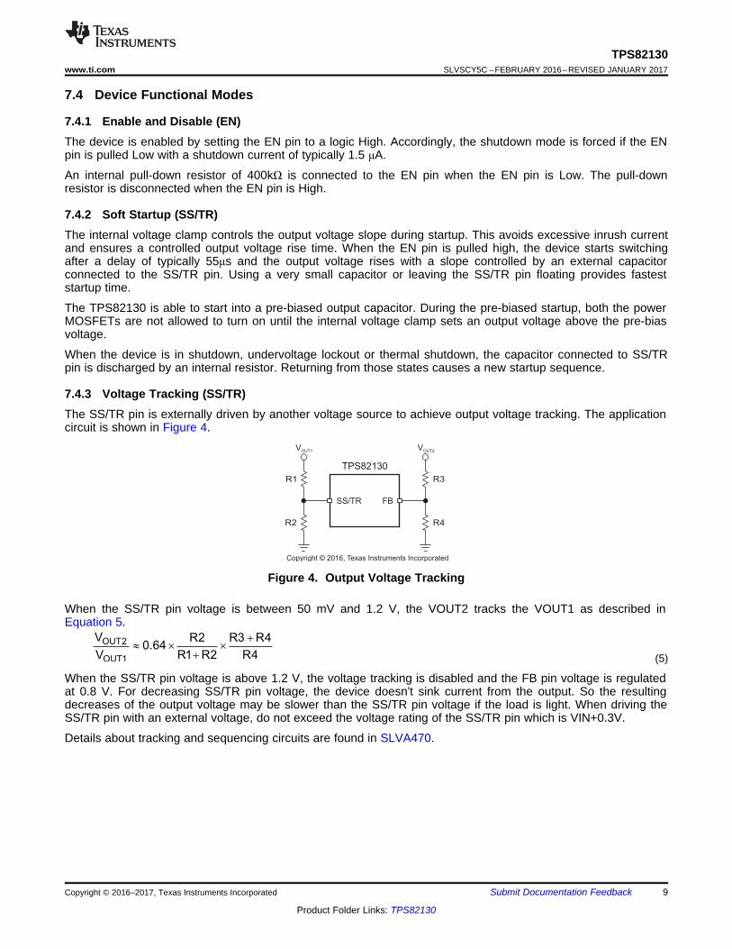
7.4.3 Voltage Tracking (SS/TR)The SS/TR pin is externally driven by another voltage source to achieve output voltage tracking. The applicationcircuit is shown in Figure 4.
Figure 4. Output Voltage Tracking
When the SS/TR pin voltage is between 50 mV and 1.2 V, the VOUT2 tracks the VOUT1 as described inEquation 5.
(5)
When the SS/TR pin voltage is above 1.2 V, the voltage tracking is disabled and the FB pin voltage is regulatedat 0.8 V. For decreasing SS/TR pin voltage, the device doesn't sink current from the output. So the resultingdecreases of the output voltage may be slower than the SS/TR pin voltage if the load is light. When driving theSS/TR pin with an external voltage, do not exceed the voltage rating of the SS/TR pin which is VIN+0.3V.
Details about tracking and sequencing circuits are found in SLVA470.
10
TPS82130SLVSCY5C –FEBRUARY 2016–REVISED JANUARY 2017 www.ti.com
Product Folder Links: TPS82130
Submit Documentation Feedback Copyright © 2016–2017, Texas Instruments Incorporated
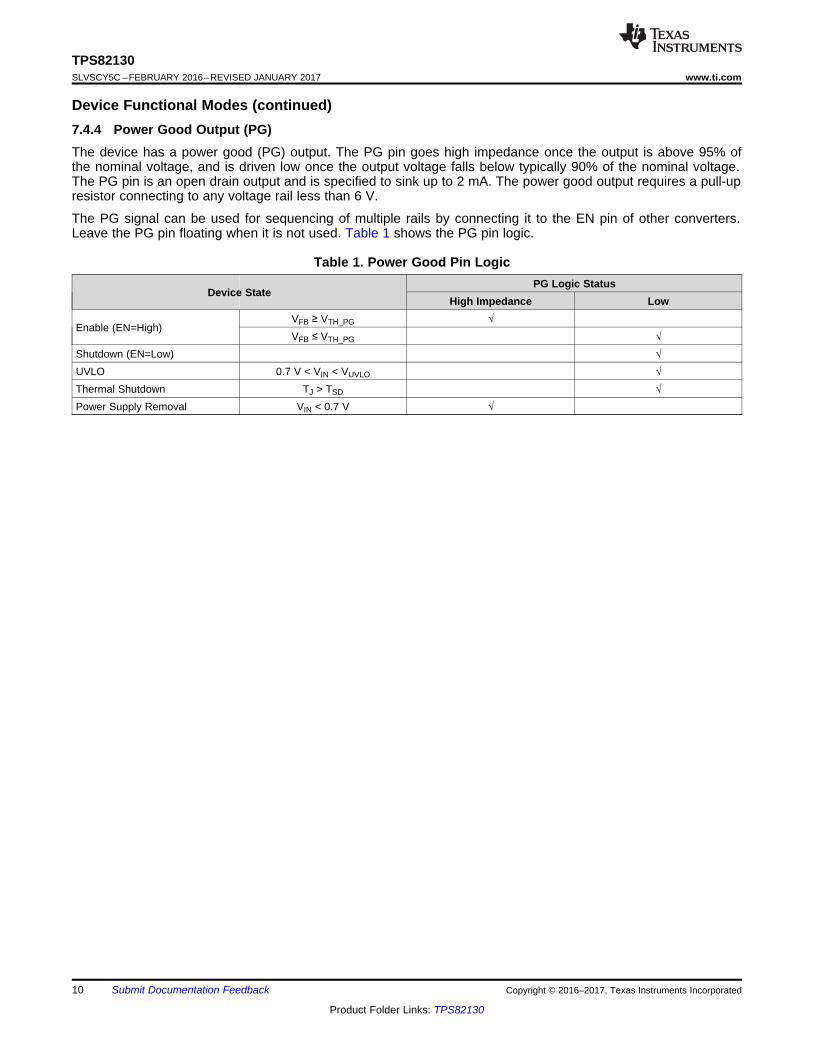
Device Functional Modes (continued)7.4.4 Power Good Output (PG)The device has a power good (PG) output. The PG pin goes high impedance once the output is above 95% ofthe nominal voltage, and is driven low once the output voltage falls below typically 90% of the nominal voltage.The PG pin is an open drain output and is specified to sink up to 2 mA. The power good output requires a pull-upresistor connecting to any voltage rail less than 6 V.
The PG signal can be used for sequencing of multiple rails by connecting it to the EN pin of other converters.Leave the PG pin floating when it is not used. Table 1 shows the PG pin logic.
Table 1. Power Good Pin Logic
Device StatePG Logic Status
High Impedance Low
Enable (EN=High)VFB ≥ VTH_PG √VFB ≤ VTH_PG √
Shutdown (EN=Low) √UVLO 0.7 V < VIN < VUVLO √Thermal Shutdown TJ > TSD √Power Supply Removal VIN < 0.7 V √
TPS82130
12 VR1124kΩ
R2100kΩ
VIN
POWER GOOD
VIN
EN
C222µF
R3100kΩ
VOUT
1.8 V/3 AC110µF
SS/TR
GNDPG
FB
VOUT
C33.3nF
Copyright © 2016, Texas Instruments Incorporated
11
TPS82130www.ti.com SLVSCY5C –FEBRUARY 2016–REVISED JANUARY 2017
Product Folder Links: TPS82130
Submit Documentation FeedbackCopyright © 2016–2017, Texas Instruments Incorporated
8 Application and Implementation
NOTEInformation in the following applications sections is not part of the TI componentspecification, and TI does not warrant its accuracy or completeness. TI’s customers areresponsible for determining suitability of components for their purposes. Customers shouldvalidate and test their design implementation to confirm system functionality.
8.1 Application InformationThe output voltage of the TPS82130 is adjusted by component selection. The following section discusses thedesign of the external components to complete the power supply design for several input and output voltageoptions by using typical applications as a reference.
8.2 Typical Applications
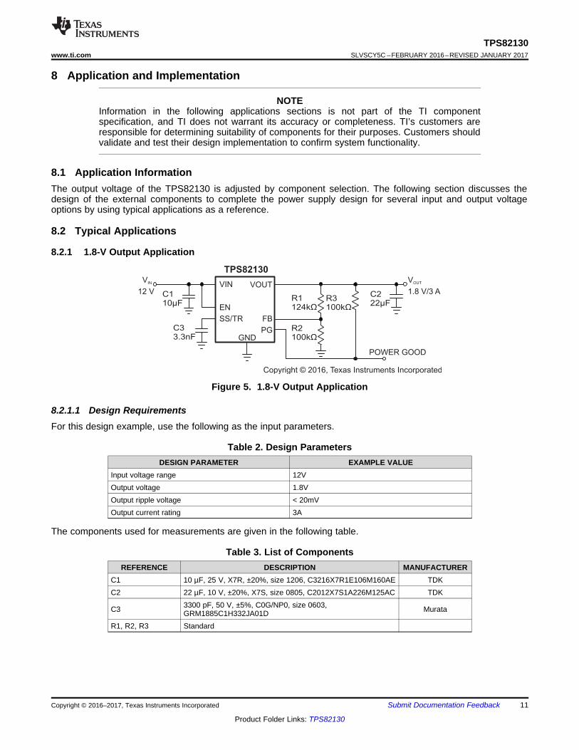
8.2.1 1.8-V Output Application
Figure 5. 1.8-V Output Application
8.2.1.1 Design RequirementsFor this design example, use the following as the input parameters.
Table 2. Design ParametersDESIGN PARAMETER EXAMPLE VALUE
Input voltage range 12VOutput voltage 1.8VOutput ripple voltage < 20mVOutput current rating 3A
The components used for measurements are given in the following table.
Table 3. List of ComponentsREFERENCE DESCRIPTION MANUFACTURER
C1 10 µF, 25 V, X7R, ±20%, size 1206, C3216X7R1E106M160AE TDKC2 22 µF, 10 V, ±20%, X7S, size 0805, C2012X7S1A226M125AC TDK
C3 3300 pF, 50 V, ±5%, C0G/NP0, size 0603,GRM1885C1H332JA01D Murata
R1, R2, R3 Standard

V25.1
ItC
TR/SSTR/SSTR/SS ´=
OUT FB
R1 R1V = V 1 + = 0.8 V 1 +
R2 R2
æ ö æ ö´ ´ç ÷ ç ÷
è ø è ø
12
TPS82130SLVSCY5C –FEBRUARY 2016–REVISED JANUARY 2017 www.ti.com
Product Folder Links: TPS82130
Submit Documentation Feedback Copyright © 2016–2017, Texas Instruments Incorporated
8.2.1.2 Detailed Design Procedure
8.2.1.2.1 Custom Design with WEBENCH® Tools
Click here to create a custom design using the TLV62090 device with the WEBENCH® Power Designer.1. Start by entering your VIN, VOUT, and IOUT requirements.2. Optimize your design for key parameters like efficiency, footprint and cost using the optimizer dial and
compare this design with other possible solutions from Texas Instruments.3. The WEBENCH Power Designer provides you with a customized schematic along with a list of materials with
real time pricing and component availability.4. In most cases, you will also be able to:
– Run electrical simulations to see important waveforms and circuit performance– Run thermal simulations to understand the thermal performance of your board– Export your customized schematic and layout into popular CAD formats– Print PDF reports for the design, and share your design with colleagues
5. Get more information about WEBENCH tools at www.ti.com/WEBENCH.
8.2.1.2.2 Setting the Output Voltage
The output voltage is set by an external resistor divider according to the following equations:
(6)
R2 should not be higher than 100kΩ to achieve high efficiency at light load while providing acceptable noisesensitivity. Larger currents through R2 improve noise sensitivity and output voltage accuracy. Figure 5 shows theexternal resistor divider value for a 1.8-V output. Choose appropriate resistor values for other outputs.
In case the FB pin gets opened, the device clamps the output voltage at the VOUT pin internally to about 7V.
8.2.1.2.3 Input and Output Capacitor Selection
For best output and input voltage filtering, low ESR ceramic capacitors are required. The input capacitorminimizes input voltage ripple, suppresses input voltage spikes and provides a stable system rail for the device.A 10-µF or larger input capacitor is required. The output capacitor value can range from 22μF up to more than400μF. Higher values are possible as well and can be evaluated through the transient response. Larger soft starttimes are recommended for higher output capacitances.
High capacitance ceramic capacitors have a DC Bias effect, which will have a strong influence on the finaleffective capacitance. Therefore the right capacitor value has to be chosen carefully. Package size and voltagerating in combination with dielectric material are responsible for differences between the rated capacitor valueand the effective capacitance.
8.2.1.2.4 Soft Startup Capacitor Selection
A capacitance connected between the SS/TR pin and the GND allows programming the startup slope of theoutput voltage. A constant current of 2.5 μA charges the external capacitor. The capacitance required for a givensoft startup time for the output voltage is given by:
(7)
Load (A)
Effi
cien
cy (
%)
50
60
70
80
90
100
1m 10m 100m 1 5
D003
VIN = 3.3 VVIN = 5.0 VVIN = 12 V
Input Voltage (V)
Effi
cien
cy (
%)
3 5 7 9 11 13 15 1750
60
70
80
90
100
D021
IOUT = 0.1 AIOUT = 1.0 AIOUT = 3.0 A
Load (A)
Effi
cien
cy (
%)
50
60
70
80
90
100
1m 10m 100m 1 5
D002
VIN = 3.3 VVIN = 5.0 VVIN = 12 V
Input Voltage (V)
Effi
cien
cy (
%)
3 5 7 9 11 13 15 1750
60
70
80
90
100
D020
IOUT = 0.1 AIOUT = 1.0 AIOUT = 3.0 A
Load (A)
Effi
cien
cy (
%)
50
60
70
80
90
100
1m 10m 100m 1 5
D001
VIN = 3.3 VVIN = 5.0 VVIN = 12 V
Input Voltage (V)
Effi
cien
cy (
%)
3 5 7 9 11 13 15 1750
60
70
80
90
100
D019
IOUT = 0.1 AIOUT = 1.0 AIOUT = 3.0 A
13
TPS82130www.ti.com SLVSCY5C –FEBRUARY 2016–REVISED JANUARY 2017
Product Folder Links: TPS82130
Submit Documentation FeedbackCopyright © 2016–2017, Texas Instruments Incorporated
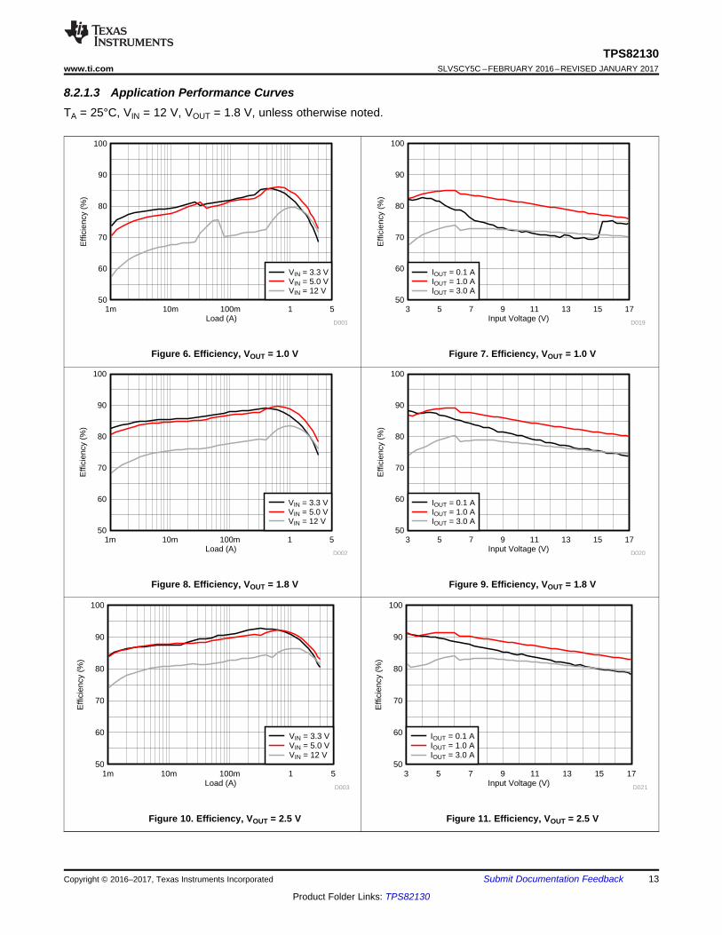
8.2.1.3 Application Performance CurvesTA = 25°C, VIN = 12 V, VOUT = 1.8 V, unless otherwise noted.
Figure 6. Efficiency, VOUT = 1.0 V Figure 7. Efficiency, VOUT = 1.0 V
Figure 8. Efficiency, VOUT = 1.8 V Figure 9. Efficiency, VOUT = 1.8 V
Figure 10. Efficiency, VOUT = 2.5 V Figure 11. Efficiency, VOUT = 2.5 V

Ambient Temperature (°C)
Out
put C
urre
nt (
A)
45 55 65 75 85 95 105 115 1250
1
2
3
4
D015
VIN = 3.3 VVIN = 5.0 VVIN = 12 V
Ambient Temperature (°C)
Out
put C
urre
nt (
A)
45 55 65 75 85 95 105 115 1250
1
2
3
4
D016
VIN = 5.0 VVIN = 12 V
Load (A)
Effi
cien
cy (
%)
50
60
70
80
90
100
1m 10m 100m 1 5
D023
VIN = 12 V
Input Voltage (V)
Effi
cien
cy (
%)
6 7 8 9 10 11 12 13 14 15 16 1750
60
70
80
90
100
D024
IOUT = 0.1 AIOUT = 1.0 AIOUT = 3.0 A
Load (A)
Effi
cien
cy (
%)
50
60
70
80
90
100
1m 10m 100m 1 5
D004
VIN = 5.0 VVIN = 12 V
Input Voltage (V)
Effi
cien
cy (
%)
5 7 9 11 13 15 1750
60
70
80
90
100
D022
IOUT = 0.1 AIOUT = 1.0 AIOUT = 3.0 A
14
TPS82130SLVSCY5C –FEBRUARY 2016–REVISED JANUARY 2017 www.ti.com
Product Folder Links: TPS82130
Submit Documentation Feedback Copyright © 2016–2017, Texas Instruments Incorporated
Figure 12. Efficiency, VOUT = 3.3 V Figure 13. Efficiency, VOUT = 3.3 V
Figure 14. Efficiency, VOUT = 5.0 V Figure 15. Efficiency, VOUT = 5.0 V
VOUT = 1.8V θJA = 46.1 °C/W
Figure 16. Thermal Derating, VOUT = 1.8 V
VOUT = 3.3V θJA = 46.1 °C/W
Figure 17. Thermal Derating, VOUT = 3.3 V
Input Voltage (V)
Sw
itchi
ng F
requ
ency
(H
z)
3 5 7 9 11 13 15 170x100
1x10⁶
2x10⁶
3x10⁶
D018
VOUT = 1.0 VVOUT = 1.8 VVOUT = 2.5 VVOUT = 3.3 V
Time - 500ns/DIV
D007
VIN50mV/DIV
AC
VOUT10mV/DIV
AC
Load (A)
Sw
itchi
ng F
requ
ency
(H
z)
103
104
105
106
5x10⁶
1m 10m 100m 1 5
D009
TA = 25°CTA = -40°CTA = 85°C
Input Voltage (V)
Out
put V
olta
ge A
ccur
acy
(%)
3 5 7 9 11 13 15 17-1.0
-0.5
0.0
0.5
1.0
D006
TA = -40°CTA = 25°CTA = 85°C
Ambient Temperature (°C)
Out
put C
urre
nt (
A)
45 55 65 75 85 95 105 115 1250
1
2
3
4
D027
VIN = 3.3 VVIN = 5.0 VVIN = 12 V
Load (A)
Out
put V
olta
ge A
ccur
acy
(%)
-1.0
-0.5
0.0
0.5
1.0
1m 10m 100m 1 5
D005
TA = -40°CTA = 25°CTA = 85°C
15
TPS82130www.ti.com SLVSCY5C –FEBRUARY 2016–REVISED JANUARY 2017
Product Folder Links: TPS82130
Submit Documentation FeedbackCopyright © 2016–2017, Texas Instruments Incorporated
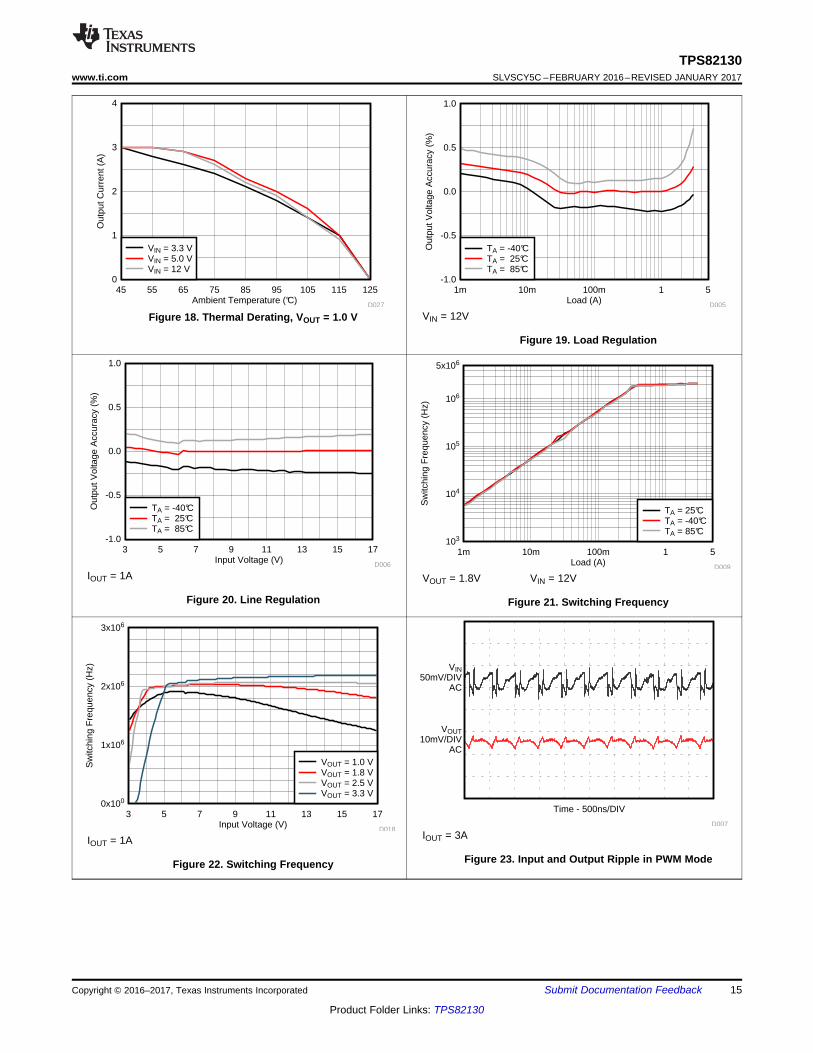
Figure 18. Thermal Derating, VOUT = 1.0 V VIN = 12V
Figure 19. Load Regulation
IOUT = 1A
Figure 20. Line Regulation
VOUT = 1.8V VIN = 12V
Figure 21. Switching Frequency
IOUT = 1A
Figure 22. Switching Frequency
IOUT = 3A
Figure 23. Input and Output Ripple in PWM Mode

7LPHV',9
D013
IOUT2A/DIV
VOUT1V/DIV
VPG5V/DIV
VEN5V/DIV
7LPHV',9
D011
IOUT2A/DIV
VOUT50mV/DIV
AC
7LPHV',9
D012
IOUT2A/DIV
VOUT1V/DIV
VPG5V/DIV
VEN5V/DIV
7LPHV',9
D008
VIN20mV/DIV
AC
VOUT10mV/DIV
AC
7LPHV',9
D010
IOUT2A/DIV
VOUT50mV/DIV
AC
16
TPS82130SLVSCY5C –FEBRUARY 2016–REVISED JANUARY 2017 www.ti.com
Product Folder Links: TPS82130
Submit Documentation Feedback Copyright © 2016–2017, Texas Instruments Incorporated
No Load
Figure 24. Input and Output Ripple in PSM Mode
IOUT = 0A to 3A, 1A/µs
Figure 25. Load Transient
IOUT = 0.5A to 3A, 1A/µs
Figure 26. Load Transient
No Load
Figure 27. Startup without Load
ROUT = 0.68Ω
Figure 28. Startup / Shutdown with Resistance Load
VIN
GND
VOUT
C3
C2
C1
VIN
VOUT
FBGND
EN
PG
SS/TR
VOUT
R1
R2
IN
OUTOUTIN
V
IV1I
´´
h=
17
TPS82130www.ti.com SLVSCY5C –FEBRUARY 2016–REVISED JANUARY 2017
Product Folder Links: TPS82130
Submit Documentation FeedbackCopyright © 2016–2017, Texas Instruments Incorporated
9 Power Supply RecommendationsThe devices are designed to operate from an input voltage supply range between 3V and 17V. The averageinput current of the TPS82130 is calculated as:
(8)Ensure that the power supply has a sufficient current rating for the applications.
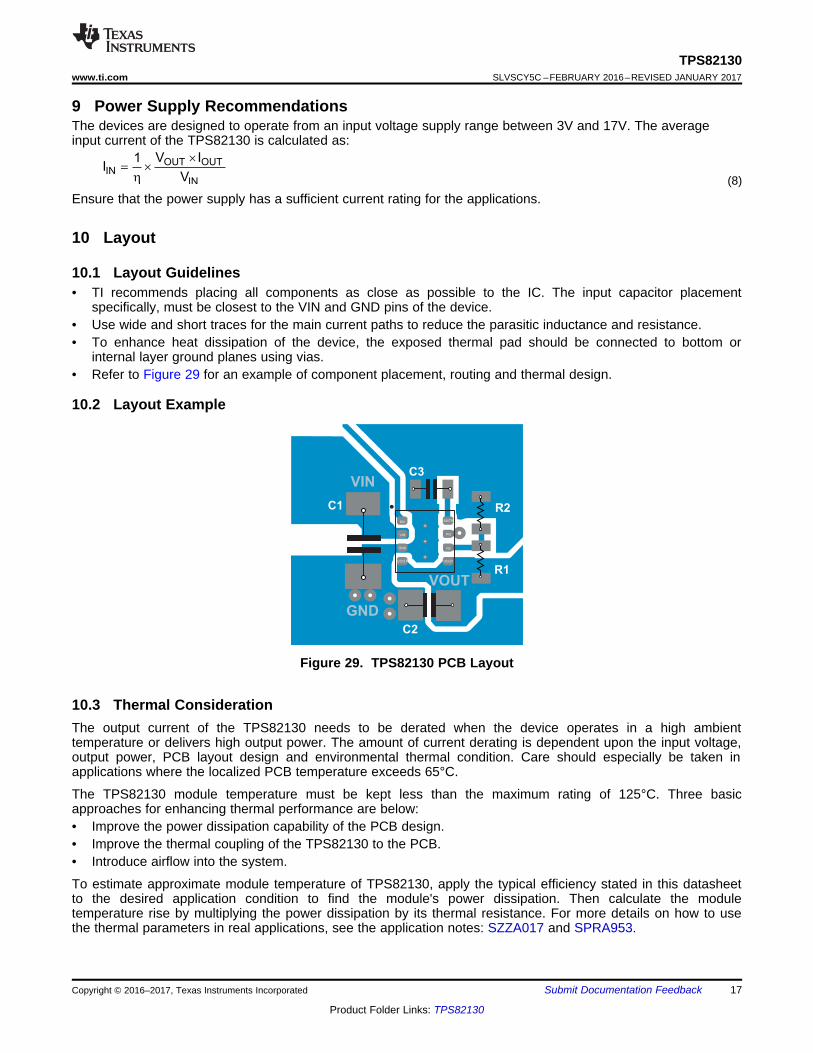
10 Layout
10.1 Layout Guidelines• TI recommends placing all components as close as possible to the IC. The input capacitor placement
specifically, must be closest to the VIN and GND pins of the device.• Use wide and short traces for the main current paths to reduce the parasitic inductance and resistance.• To enhance heat dissipation of the device, the exposed thermal pad should be connected to bottom or
internal layer ground planes using vias.• Refer to Figure 29 for an example of component placement, routing and thermal design.
10.2 Layout Example
Figure 29. TPS82130 PCB Layout
10.3 Thermal ConsiderationThe output current of the TPS82130 needs to be derated when the device operates in a high ambienttemperature or delivers high output power. The amount of current derating is dependent upon the input voltage,output power, PCB layout design and environmental thermal condition. Care should especially be taken inapplications where the localized PCB temperature exceeds 65°C.
The TPS82130 module temperature must be kept less than the maximum rating of 125°C. Three basicapproaches for enhancing thermal performance are below:• Improve the power dissipation capability of the PCB design.• Improve the thermal coupling of the TPS82130 to the PCB.• Introduce airflow into the system.
To estimate approximate module temperature of TPS82130, apply the typical efficiency stated in this datasheetto the desired application condition to find the module's power dissipation. Then calculate the moduletemperature rise by multiplying the power dissipation by its thermal resistance. For more details on how to usethe thermal parameters in real applications, see the application notes: SZZA017 and SPRA953.
18
TPS82130SLVSCY5C –FEBRUARY 2016–REVISED JANUARY 2017 www.ti.com
Product Folder Links: TPS82130
Submit Documentation Feedback Copyright © 2016–2017, Texas Instruments Incorporated
11 Device and Documentation Support
11.1 Development Support
11.1.1 Custom Design with WEBENCH® ToolsClick here to create a custom design using the TLV62090 device with the WEBENCH® Power Designer.1. Start by entering your VIN, VOUT, and IOUT requirements.2. Optimize your design for key parameters like efficiency, footprint and cost using the optimizer dial and
compare this design with other possible solutions from Texas Instruments.3. The WEBENCH Power Designer provides you with a customized schematic along with a list of materials with
real time pricing and component availability.4. In most cases, you will also be able to:
– Run electrical simulations to see important waveforms and circuit performance– Run thermal simulations to understand the thermal performance of your board– Export your customized schematic and layout into popular CAD formats– Print PDF reports for the design, and share your design with colleagues
5. Get more information about WEBENCH tools at www.ti.com/WEBENCH.
11.2 Receiving Notification of Documentation UpdatesTo receive notification of documentation updates, navigate to the device product folder on ti.com. In the upperright corner, click on Alert me to register and receive a weekly digest of any product information that haschanged. For change details, review the revision history included in any revised document.
11.3 Community ResourcesThe following links connect to TI community resources. Linked contents are provided "AS IS" by the respectivecontributors. They do not constitute TI specifications and do not necessarily reflect TI's views; see TI's Terms ofUse.
TI E2E™ Online Community TI's Engineer-to-Engineer (E2E) Community. Created to foster collaborationamong engineers. At e2e.ti.com, you can ask questions, share knowledge, explore ideas and helpsolve problems with fellow engineers.
Design Support TI's Design Support Quickly find helpful E2E forums along with design support tools andcontact information for technical support.
11.4 TrademarksMicroSiP, DCS-Control, E2E are trademarks of Texas Instruments.WEBENCH is a registered trademark of Texas Instruments.
11.5 Electrostatic Discharge CautionThese devices have limited built-in ESD protection. The leads should be shorted together or the device placed in conductive foamduring storage or handling to prevent electrostatic damage to the MOS gates.
11.6 GlossarySLYZ022 — TI Glossary.
This glossary lists and explains terms, acronyms, and definitions.
12 Mechanical, Packaging, and Orderable InformationThe following pages include mechanical, packaging, and orderable information. This information is the mostcurrent data available for the designated devices. This data is subject to change without notice and revision ofthis document. For browser-based versions of this data sheet, refer to the left-hand navigation.
www.ti.com
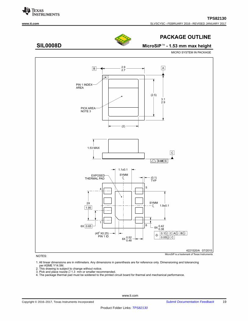
PACKAGE OUTLINE
C
B2.92.7
A
3.12.9
(45 X0.25)PIN 1 ID
2X
1.95
6X 0.65
(0.1)TYP
8X0.420.38
8X0.520.48
1.53 MAX
1.9±0.1
1.1±0.1
(2.5)
(2)
MicroSiP - 1.53 mm max heightSIL0008DMICRO SYSTEM IN PACKAGE
4221520/A 07/2015
PIN 1 INDEXAREA
PICK AREANOTE 3
0.08 C
0.1 C A B
0.05 C
1
45
8
SYMM
SYMM
THERMAL PADEXPOSED
NOTES:
1. All linear dimensions are in millimeters. Any dimensions in parenthesis are for reference only. Dimensioning and tolerancingper ASME Y14.5M.
2. This drawing is subject to change without notice.3. Pick and place nozzle 1.3 mm or smaller recommended.4. The package thermal pad must be soldered to the printed circuit board for thermal and mechanical performance.
MicroSiP is a trademark of Texas Instruments
TM
0.08 C
SCALE 4.000
19
TPS82130www.ti.com SLVSCY5C –FEBRUARY 2016–REVISED JANUARY 2017
Product Folder Links: TPS82130
Submit Documentation FeedbackCopyright © 2016–2017, Texas Instruments Incorporated
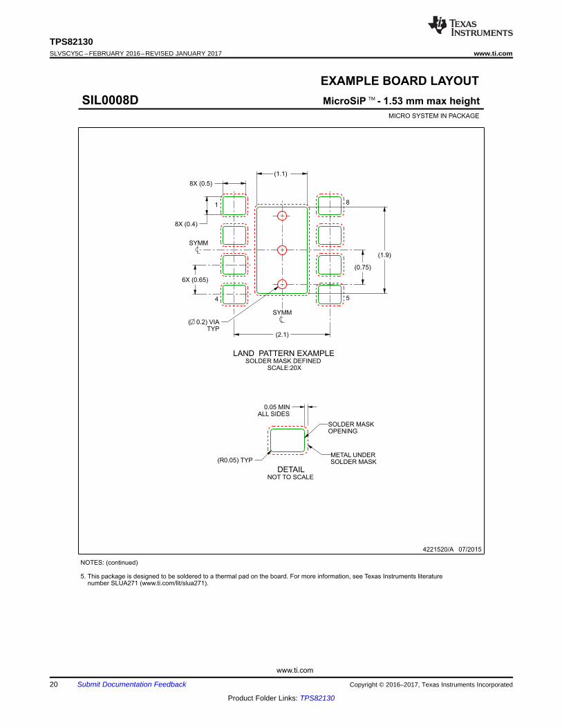
www.ti.com
EXAMPLE BOARD LAYOUT
(1.1)
8X (0.5)
0.05 MINALL SIDES
8X (0.4)
(2.1)
6X (0.65)
(0.75)
( ) VIATYP
0.2
(1.9)
(R ) TYP0.05
MicroSiP - 1.53 mm max heightSIL0008DMICRO SYSTEM IN PACKAGE
4221520/A 07/2015
SYMM
SYMM
1
4 5
8
SOLDER MASK DEFINEDLAND PATTERN EXAMPLE
SCALE:20X
NOTES: (continued)
5. This package is designed to be soldered to a thermal pad on the board. For more information, see Texas Instruments literaturenumber SLUA271 (www.ti.com/lit/slua271).
TM
METAL UNDERSOLDER MASK
SOLDER MASKOPENING
NOT TO SCALEDETAIL
20
TPS82130SLVSCY5C –FEBRUARY 2016–REVISED JANUARY 2017 www.ti.com
Product Folder Links: TPS82130
Submit Documentation Feedback Copyright © 2016–2017, Texas Instruments Incorporated
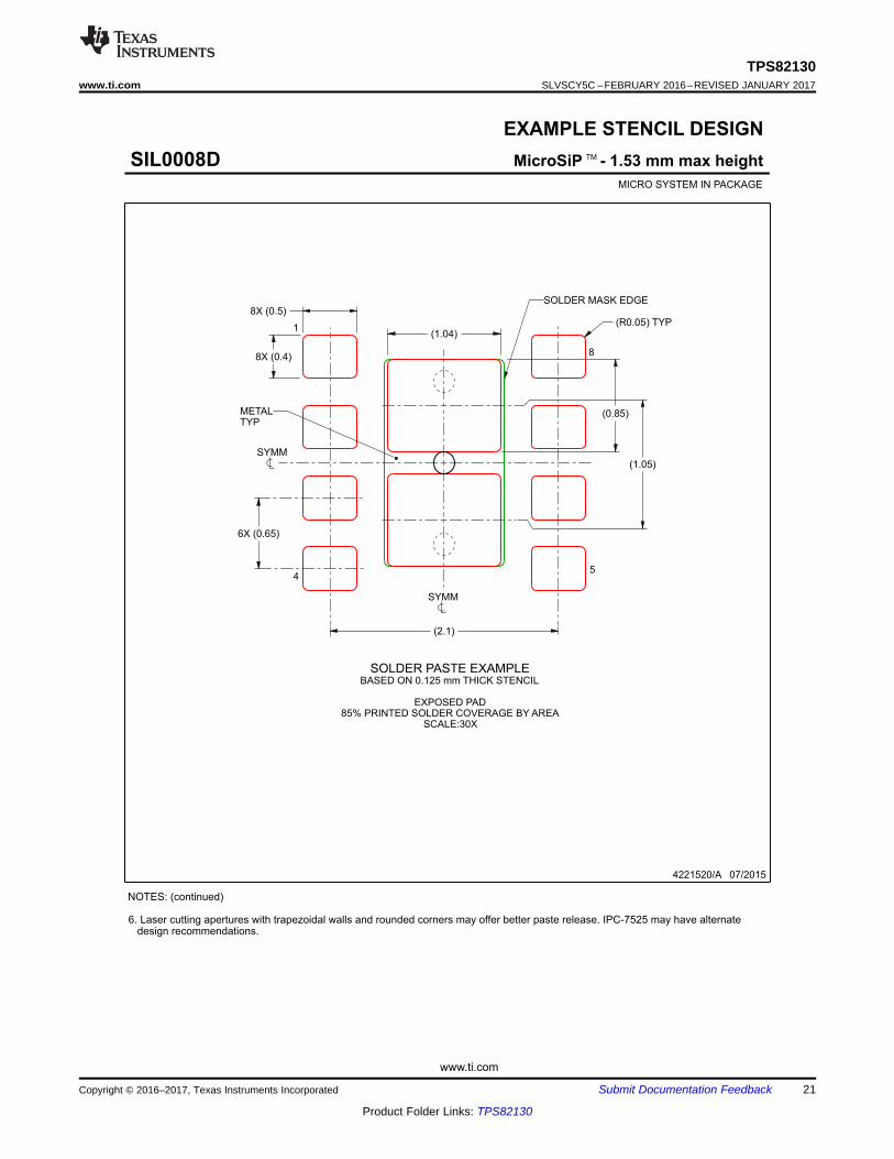
www.ti.com
EXAMPLE STENCIL DESIGN
(R ) TYP0.05
8X (0.4)
(1.04)
8X (0.5)
6X (0.65)
(2.1)
(0.85)
(1.05)
MicroSiP - 1.53 mm max heightSIL0008DMICRO SYSTEM IN PACKAGE
4221520/A 07/2015
NOTES: (continued)
6. Laser cutting apertures with trapezoidal walls and rounded corners may offer better paste release. IPC-7525 may have alternatedesign recommendations.
TM
SYMM
SYMM
METALTYP
BASED ON 0.125 mm THICK STENCILSOLDER PASTE EXAMPLE
EXPOSED PAD85% PRINTED SOLDER COVERAGE BY AREA
SCALE:30X
SOLDER MASK EDGE
1
45
8
21
TPS82130www.ti.com SLVSCY5C –FEBRUARY 2016–REVISED JANUARY 2017
Product Folder Links: TPS82130
Submit Documentation FeedbackCopyright © 2016–2017, Texas Instruments Incorporated
PACKAGE OPTION ADDENDUM
www.ti.com 30-Jun-2018
Addendum-Page 1
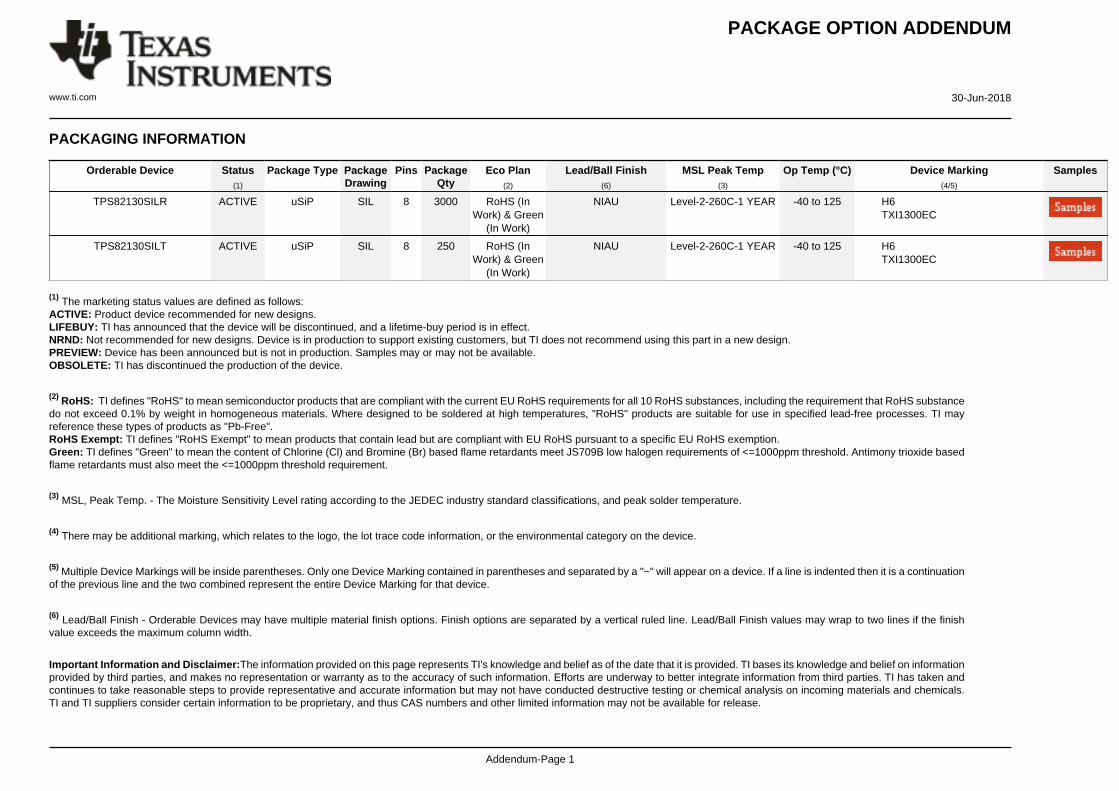
PACKAGING INFORMATION
Orderable Device Status(1)
Package Type PackageDrawing
Pins PackageQty
Eco Plan(2)
Lead/Ball Finish(6)
MSL Peak Temp(3)
Op Temp (°C) Device Marking(4/5)
Samples
TPS82130SILR ACTIVE uSiP SIL 8 3000 RoHS (InWork) & Green
(In Work)
NIAU Level-2-260C-1 YEAR -40 to 125 H6TXI1300EC
TPS82130SILT ACTIVE uSiP SIL 8 250 RoHS (InWork) & Green
(In Work)
NIAU Level-2-260C-1 YEAR -40 to 125 H6TXI1300EC
(1) The marketing status values are defined as follows:ACTIVE: Product device recommended for new designs.LIFEBUY: TI has announced that the device will be discontinued, and a lifetime-buy period is in effect.NRND: Not recommended for new designs. Device is in production to support existing customers, but TI does not recommend using this part in a new design.PREVIEW: Device has been announced but is not in production. Samples may or may not be available.OBSOLETE: TI has discontinued the production of the device.
(2) RoHS: TI defines "RoHS" to mean semiconductor products that are compliant with the current EU RoHS requirements for all 10 RoHS substances, including the requirement that RoHS substancedo not exceed 0.1% by weight in homogeneous materials. Where designed to be soldered at high temperatures, "RoHS" products are suitable for use in specified lead-free processes. TI mayreference these types of products as "Pb-Free".RoHS Exempt: TI defines "RoHS Exempt" to mean products that contain lead but are compliant with EU RoHS pursuant to a specific EU RoHS exemption.Green: TI defines "Green" to mean the content of Chlorine (Cl) and Bromine (Br) based flame retardants meet JS709B low halogen requirements of <=1000ppm threshold. Antimony trioxide basedflame retardants must also meet the <=1000ppm threshold requirement.
(3) MSL, Peak Temp. - The Moisture Sensitivity Level rating according to the JEDEC industry standard classifications, and peak solder temperature.
(4) There may be additional marking, which relates to the logo, the lot trace code information, or the environmental category on the device.
(5) Multiple Device Markings will be inside parentheses. Only one Device Marking contained in parentheses and separated by a "~" will appear on a device. If a line is indented then it is a continuationof the previous line and the two combined represent the entire Device Marking for that device.
(6) Lead/Ball Finish - Orderable Devices may have multiple material finish options. Finish options are separated by a vertical ruled line. Lead/Ball Finish values may wrap to two lines if the finishvalue exceeds the maximum column width.
Important Information and Disclaimer:The information provided on this page represents TI's knowledge and belief as of the date that it is provided. TI bases its knowledge and belief on informationprovided by third parties, and makes no representation or warranty as to the accuracy of such information. Efforts are underway to better integrate information from third parties. TI has taken andcontinues to take reasonable steps to provide representative and accurate information but may not have conducted destructive testing or chemical analysis on incoming materials and chemicals.TI and TI suppliers consider certain information to be proprietary, and thus CAS numbers and other limited information may not be available for release.

PACKAGE OPTION ADDENDUM
www.ti.com 30-Jun-2018
Addendum-Page 2
In no event shall TI's liability arising out of such information exceed the total purchase price of the TI part(s) at issue in this document sold by TI to Customer on an annual basis.

IMPORTANT NOTICE
Texas Instruments Incorporated (TI) reserves the right to make corrections, enhancements, improvements and other changes to itssemiconductor products and services per JESD46, latest issue, and to discontinue any product or service per JESD48, latest issue. Buyersshould obtain the latest relevant information before placing orders and should verify that such information is current and complete.TI’s published terms of sale for semiconductor products (http://www.ti.com/sc/docs/stdterms.htm) apply to the sale of packaged integratedcircuit products that TI has qualified and released to market. Additional terms may apply to the use or sale of other types of TI products andservices.Reproduction of significant portions of TI information in TI data sheets is permissible only if reproduction is without alteration and isaccompanied by all associated warranties, conditions, limitations, and notices. TI is not responsible or liable for such reproduceddocumentation. Information of third parties may be subject to additional restrictions. Resale of TI products or services with statementsdifferent from or beyond the parameters stated by TI for that product or service voids all express and any implied warranties for theassociated TI product or service and is an unfair and deceptive business practice. TI is not responsible or liable for any such statements.Buyers and others who are developing systems that incorporate TI products (collectively, “Designers”) understand and agree that Designersremain responsible for using their independent analysis, evaluation and judgment in designing their applications and that Designers havefull and exclusive responsibility to assure the safety of Designers' applications and compliance of their applications (and of all TI productsused in or for Designers’ applications) with all applicable regulations, laws and other applicable requirements. Designer represents that, withrespect to their applications, Designer has all the necessary expertise to create and implement safeguards that (1) anticipate dangerousconsequences of failures, (2) monitor failures and their consequences, and (3) lessen the likelihood of failures that might cause harm andtake appropriate actions. Designer agrees that prior to using or distributing any applications that include TI products, Designer willthoroughly test such applications and the functionality of such TI products as used in such applications.TI’s provision of technical, application or other design advice, quality characterization, reliability data or other services or information,including, but not limited to, reference designs and materials relating to evaluation modules, (collectively, “TI Resources”) are intended toassist designers who are developing applications that incorporate TI products; by downloading, accessing or using TI Resources in anyway, Designer (individually or, if Designer is acting on behalf of a company, Designer’s company) agrees to use any particular TI Resourcesolely for this purpose and subject to the terms of this Notice.TI’s provision of TI Resources does not expand or otherwise alter TI’s applicable published warranties or warranty disclaimers for TIproducts, and no additional obligations or liabilities arise from TI providing such TI Resources. TI reserves the right to make corrections,enhancements, improvements and other changes to its TI Resources. TI has not conducted any testing other than that specificallydescribed in the published documentation for a particular TI Resource.Designer is authorized to use, copy and modify any individual TI Resource only in connection with the development of applications thatinclude the TI product(s) identified in such TI Resource. NO OTHER LICENSE, EXPRESS OR IMPLIED, BY ESTOPPEL OR OTHERWISETO ANY OTHER TI INTELLECTUAL PROPERTY RIGHT, AND NO LICENSE TO ANY TECHNOLOGY OR INTELLECTUAL PROPERTYRIGHT OF TI OR ANY THIRD PARTY IS GRANTED HEREIN, including but not limited to any patent right, copyright, mask work right, orother intellectual property right relating to any combination, machine, or process in which TI products or services are used. Informationregarding or referencing third-party products or services does not constitute a license to use such products or services, or a warranty orendorsement thereof. Use of TI Resources may require a license from a third party under the patents or other intellectual property of thethird party, or a license from TI under the patents or other intellectual property of TI.TI RESOURCES ARE PROVIDED “AS IS” AND WITH ALL FAULTS. TI DISCLAIMS ALL OTHER WARRANTIES ORREPRESENTATIONS, EXPRESS OR IMPLIED, REGARDING RESOURCES OR USE THEREOF, INCLUDING BUT NOT LIMITED TOACCURACY OR COMPLETENESS, TITLE, ANY EPIDEMIC FAILURE WARRANTY AND ANY IMPLIED WARRANTIES OFMERCHANTABILITY, FITNESS FOR A PARTICULAR PURPOSE, AND NON-INFRINGEMENT OF ANY THIRD PARTY INTELLECTUALPROPERTY RIGHTS. TI SHALL NOT BE LIABLE FOR AND SHALL NOT DEFEND OR INDEMNIFY DESIGNER AGAINST ANY CLAIM,INCLUDING BUT NOT LIMITED TO ANY INFRINGEMENT CLAIM THAT RELATES TO OR IS BASED ON ANY COMBINATION OFPRODUCTS EVEN IF DESCRIBED IN TI RESOURCES OR OTHERWISE. IN NO EVENT SHALL TI BE LIABLE FOR ANY ACTUAL,DIRECT, SPECIAL, COLLATERAL, INDIRECT, PUNITIVE, INCIDENTAL, CONSEQUENTIAL OR EXEMPLARY DAMAGES INCONNECTION WITH OR ARISING OUT OF TI RESOURCES OR USE THEREOF, AND REGARDLESS OF WHETHER TI HAS BEENADVISED OF THE POSSIBILITY OF SUCH DAMAGES.Unless TI has explicitly designated an individual product as meeting the requirements of a particular industry standard (e.g., ISO/TS 16949and ISO 26262), TI is not responsible for any failure to meet such industry standard requirements.Where TI specifically promotes products as facilitating functional safety or as compliant with industry functional safety standards, suchproducts are intended to help enable customers to design and create their own applications that meet applicable functional safety standardsand requirements. Using products in an application does not by itself establish any safety features in the application. Designers mustensure compliance with safety-related requirements and standards applicable to their applications. Designer may not use any TI products inlife-critical medical equipment unless authorized officers of the parties have executed a special contract specifically governing such use.Life-critical medical equipment is medical equipment where failure of such equipment would cause serious bodily injury or death (e.g., lifesupport, pacemakers, defibrillators, heart pumps, neurostimulators, and implantables). Such equipment includes, without limitation, allmedical devices identified by the U.S. Food and Drug Administration as Class III devices and equivalent classifications outside the U.S.TI may expressly designate certain products as completing a particular qualification (e.g., Q100, Military Grade, or Enhanced Product).Designers agree that it has the necessary expertise to select the product with the appropriate qualification designation for their applicationsand that proper product selection is at Designers’ own risk. Designers are solely responsible for compliance with all legal and regulatoryrequirements in connection with such selection.Designer will fully indemnify TI and its representatives against any damages, costs, losses, and/or liabilities arising out of Designer’s non-compliance with the terms and provisions of this Notice.
Mailing Address: Texas Instruments, Post Office Box 655303, Dallas, Texas 75265Copyright © 2018, Texas Instruments Incorporated


![Origami Three-Headed Dragonorig08.deviantart.net/d017/f/2009/191/2/a/3_headed_dragon_instr... · Origami Three-Headed Dragon [First draft – may contain errors] Donya Quick Difficulty:](https://img.pdfslide.us/doc/110x75/5b0e6d4b7f8b9a6c388ba999/origami-three-headed-three-headed-dragon-first-draft-may-contain-errors-donya.jpg)