Embed Size (px)
Citation preview
LM7705
+
-
CRES
CFLY
COUT
+ In
- In
shutdown
low voltage amplifier
true zero output voltage-V
+V
+V
-0.23V
CF+
VSS
SD
VDD
VSS
VOUT
CRES
CF-
LM7705
www.ti.com SNVS420B –NOVEMBER 2008–REVISED MARCH 2013
LM7705 Low Noise Negative Bias GeneratorCheck for Samples: LM7705
1FEATURES DESCRIPTIONThe LM7705 is a switched capacitor voltage inverter
2• Regulated Output Voltage −0.232Vwith a low noise, −0.23V fixed negative voltage
• Output Voltage Tolerance 5% regulator. This device is designed to be used with low• Output Voltage Ripple 4 mVPP voltage amplifiers to enable the amplifiers output to
swing to zero volts. The −0.23 volts is used to supply• Max Output Current 26 mAthe negative supply pin of an amplifier while• Supply Voltage 3V to 5.25V maintaining less then 5.5 volts across the amplifier.
• Conversion Efficiency up to 98% Rail-to-Rail output amplifiers cannot output zero voltswhen operating from a single supply voltage and can• Quiescent Current 78 µAresult in error accumulation due to amplifier output• Shutdown Current 20 nAsaturation voltage being amplified by following gain
• Turn on Time 500 µs stages. A small negative supply voltage will preventthe amplifiers output from saturating at zero volts and• Operating Temperature Range −40°C to 125°Cwill help maintain an accurate zero through a signal• 8-Pin VSSOP Packageprocessing chain. Additionally, when an amplifier isused to drive an ADC’s input, it can output a zeroAPPLICATIONS voltage signal and the full input range of an ADC can
• True Zero Amplifier Output be used. The LM7705 has a shutdown pin tominimize standby power consumption• Portable Instrumentation
• Low Voltage Split Power Supplies
Typical Application
These devices have limited built-in ESD protection. The leads should be shorted together or the device placed in conductive foamduring storage or handling to prevent electrostatic damage to the MOS gates.
1
Please be aware that an important notice concerning availability, standard warranty, and use in critical applications ofTexas Instruments semiconductor products and disclaimers thereto appears at the end of this data sheet.
2All trademarks are the property of their respective owners.
PRODUCTION DATA information is current as of publication date. Copyright © 2008–2013, Texas Instruments IncorporatedProducts conform to specifications per the terms of the TexasInstruments standard warranty. Production processing does notnecessarily include testing of all parameters.
LM7705
SNVS420B –NOVEMBER 2008–REVISED MARCH 2013 www.ti.com
ABSOLUTE MAXIMUM RATINGS (1) (2)
VALUE
Supply Voltage +5.75VVDD - VSS
SD VDD+0.3V, VSS-0.3V
For input pins only 2000VHuman Body Model
For all other pins 2000VESD Tolerance (3)
Machine Model 200V
Charged Device Model 750V
Storage Temp. Range −65°C to 150°C
Junction Temperature (4) 150°C max
Mounting Temperature Infrared or Convection (20 sec) 260°C
(1) Absolute Maximum Ratings indicate limits beyond which damage to the device may occur. Operating Ratings indicate conditions forwhich the device is intended to be functional, but specific performance is not ensured. For ensured specifications and test conditions,see the Electrical Characteristics.
(2) If Military/Aerospace specified devices are required, please contact the TI Sales Office/ Distributors for availability and specifications.(3) Human Body Model, applicable std. MIL-STD-883, Method 3015.7. Machine model, applicable std JESD22–A115–A (ESSD MM srd of
JEDEC). Field induced Charge-Device Model, applicable std. JESD22–C101–C. (ESD FICDM std of JEDEC).(4) Typical values represent the most likely parametric norm as determined at the time of characterization. Actual typical values may vary
over time and will also depend on the application and configuration. The typical values are not tested and are not ensured on shippedproduction material.
Operating RatingsSupply Voltage ( VDD to GND) 3V to 5.25V
Supply Voltage ( VDD wrt VOUT) 3.23V to 5.48V
Temperature Range −40°C to 125°C
Thermal Resistance (θJA ) 8-Pin VSSOP 253°C/W
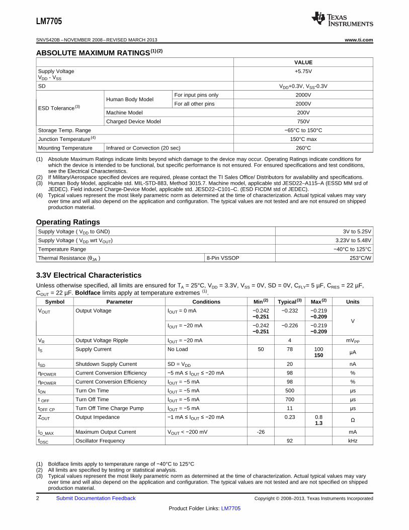
3.3V Electrical CharacteristicsUnless otherwise specified, all limits are ensured for TA = 25°C, VDD = 3.3V, VSS = 0V, SD = 0V, CFLY= 5 µF, CRES = 22 µF,COUT = 22 µF. Boldface limits apply at temperature extremes (1).
Symbol Parameter Conditions Min (2) Typical (3) Max (2) Units
VOUT Output Voltage IOUT = 0 mA −0.242 −0.232 −0.219−0.251 −0.209
VIOUT = −20 mA −0.242 −0.226 −0.219
−0.251 −0.209
VR Output Voltage Ripple IOUT = −20 mA 4 mVPP
IS Supply Current No Load 50 78 100 μA150
ISD Shutdown Supply Current SD = VDD 20 nA
ηPOWER Current Conversion Efficiency −5 mA ≤ IOUT ≤ −20 mA 98 %
ηPOWER Current Conversion Efficiency IOUT = −5 mA 98 %
tON Turn On Time IOUT = −5 mA 500 μs
t OFF Turn Off Time IOUT = −5 mA 700 μs
tOFF CP Turn Off Time Charge Pump IOUT = −5 mA 11 μs
ZOUT Output Impedance −1 mA ≤ IOUT ≤ −20 mA 0.23 0.8 Ω1.3
IO_MAX Maximum Output Current VOUT < −200 mV -26 mA
fOSC Oscillator Frequency 92 kHz
(1) Boldface limits apply to temperature range of −40°C to 125°C(2) All limits are specified by testing or statistical analysis.(3) Typical values represent the most likely parametric norm as determined at the time of characterization. Actual typical values may vary
over time and will also depend on the application and configuration. The typical values are not tested and are not specified on shippedproduction material.
2 Submit Documentation Feedback Copyright © 2008–2013, Texas Instruments Incorporated
Product Folder Links: LM7705
LM7705
www.ti.com SNVS420B –NOVEMBER 2008–REVISED MARCH 2013
3.3V Electrical Characteristics (continued)Unless otherwise specified, all limits are ensured for TA = 25°C, VDD = 3.3V, VSS = 0V, SD = 0V, CFLY= 5 µF, CRES = 22 µF,COUT = 22 µF. Boldface limits apply at temperature extremes (1).
Symbol Parameter Conditions Min (2) Typical (3) Max (2) Units
VIL Shutdown Input Low 1.6 V1.25
VIH Shutdown Input High 1.85 V2.15
IC Shutdown Pin Input Current SD = VDD 50 pA
Load Regulation 0 mA ≤ IOUT ≤ −20 mA 0.12 0.6 %/mA0.85
Line Regulation 3V ≤ VDD ≤ 5.25V (No Load) -0.2 0.29 0.7 %/V1.1
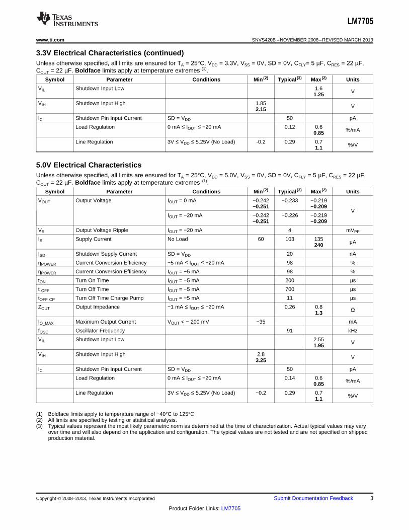
5.0V Electrical CharacteristicsUnless otherwise specified, all limits are ensured for TA = 25°C, VDD = 5.0V, VSS = 0V, SD = 0V, CFLY = 5 µF, CRES = 22 µF,COUT = 22 µF. Boldface limits apply at temperature extremes (1).
Symbol Parameter Conditions Min (2) Typical (3) Max (2) Units
VOUT Output Voltage IOUT = 0 mA −0.242 −0.233 −0.219−0.251 −0.209
VIOUT = −20 mA −0.242 −0.226 −0.219
−0.251 −0.209
VR Output Voltage Ripple IOUT = −20 mA 4 mVPP
IS Supply Current No Load 60 103 135 μA240
ISD Shutdown Supply Current SD = VDD 20 nA
ηPOWER Current Conversion Efficiency −5 mA ≤ IOUT ≤ −20 mA 98 %
ηPOWER Current Conversion Efficiency IOUT = −5 mA 98 %
tON Turn On Time IOUT = −5 mA 200 μs
t OFF Turn Off Time IOUT = −5 mA 700 μs
tOFF CP Turn Off Time Charge Pump IOUT = −5 mA 11 μs
ZOUT Output Impedance −1 mA ≤ IOUT ≤ −20 mA 0.26 0.8 Ω1.3
IO_MAX Maximum Output Current VOUT < − 200 mV −35 mA
fOSC Oscillator Frequency 91 kHz
VIL Shutdown Input Low 2.55 V1.95
VIH Shutdown Input High 2.8 V3.25
IC Shutdown Pin Input Current SD = VDD 50 pA
Load Regulation 0 mA ≤ IOUT ≤ −20 mA 0.14 0.6 %/mA0.85
Line Regulation 3V ≤ VDD ≤ 5.25V (No Load) −0.2 0.29 0.7 %/V1.1
(1) Boldface limits apply to temperature range of −40°C to 125°C(2) All limits are specified by testing or statistical analysis.(3) Typical values represent the most likely parametric norm as determined at the time of characterization. Actual typical values may vary
over time and will also depend on the application and configuration. The typical values are not tested and are not specified on shippedproduction material.
Copyright © 2008–2013, Texas Instruments Incorporated Submit Documentation Feedback 3
Product Folder Links: LM7705
CFLY
CHARGE PUMP
INVERTORCRESERVE
VREF1
PRE REGULATOR
VCP,IN
fosc
VOUT
VCP,OUT
POSTREGULATOR Cout
VDD
VSS VSS
VREF2
1
4 5
8
LM7705
LM7705
SNVS420B –NOVEMBER 2008–REVISED MARCH 2013 www.ti.com
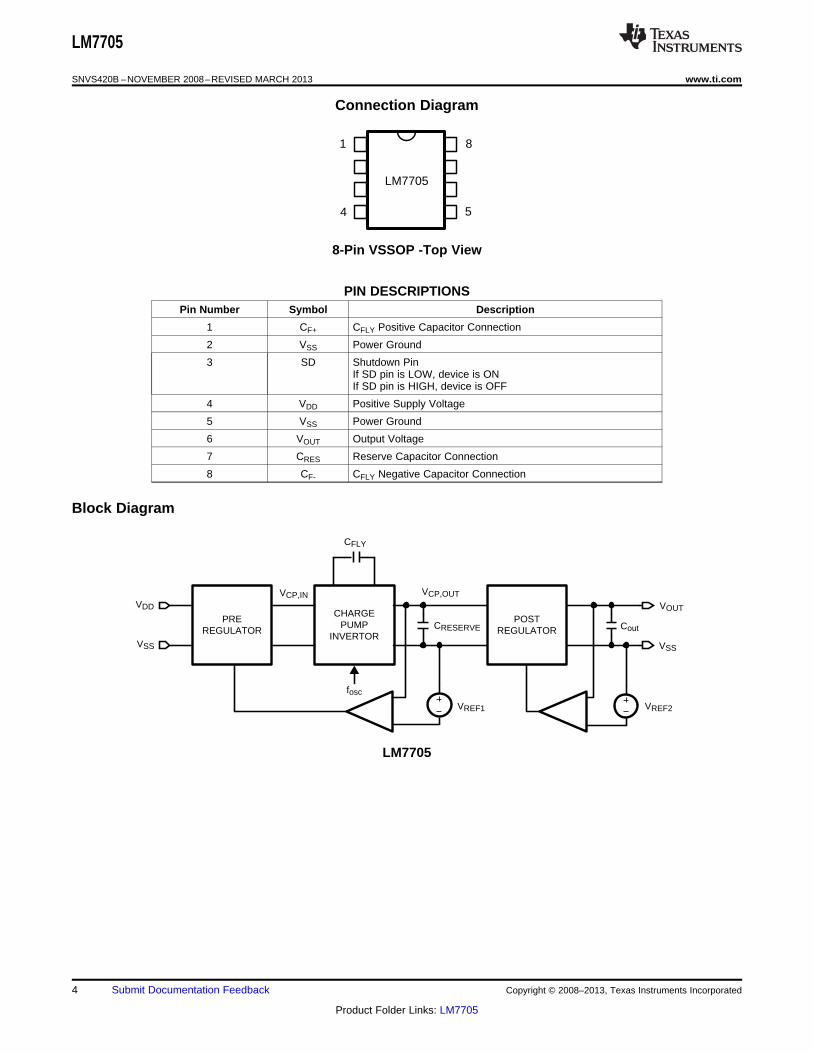
Connection Diagram
8-Pin VSSOP -Top View
PIN DESCRIPTIONSPin Number Symbol Description
1 CF+ CFLY Positive Capacitor Connection
2 VSS Power Ground
3 SD Shutdown PinIf SD pin is LOW, device is ONIf SD pin is HIGH, device is OFF
4 VDD Positive Supply Voltage
5 VSS Power Ground
6 VOUT Output Voltage
7 CRES Reserve Capacitor Connection
8 CF- CFLY Negative Capacitor Connection
Block Diagram
LM7705
4 Submit Documentation Feedback Copyright © 2008–2013, Texas Instruments Incorporated
Product Folder Links: LM7705
TEMPERATURE (°C)
OU
TP
UT
VO
LTA
GE
RIP
PLE
(mV
PP
)
15
12
9
6
3
0-40 0 40 80 120
CRES = CFILTER = 22 éF
CRES = CFILTER = 10 éF
SUPPLY VOLTAGE = 3.3V
TEMPERATURE (°C)
OU
TP
UT
VO
LTA
GE
RIP
PLE
(mV
PP
)
15
12
9
6
3
0-40 0 40 80 120
CRES = CFILTER = 22 éF
CRES = CFILTER = 10 éF
SUPPLY VOLTAGE = 5.0V
OUTPUT CURRENT (mA)
OU
TP
UT
VO
LTA
GE
(V
)
-0.20
-0.21
-0.22
-0.23
-0.24
-0.25
0 5 10 15 20 25 30
-40°C
125°C
25°C
85°C
SUPPLY VOLTAGE = 3.3V
OUTPUT CURRENT (mA)
OU
TP
UT
VO
LTA
GE
(V
)
-0.20
-0.21
-0.22
-0.23
-0.24
-0.25
0 10 20 30 40 50 60
-40°C
125°C
25°C85°C
SUPPLY VOLTAGE = 5.0V
SUPPLY VOLTAGE (V)
OU
TP
UT
VO
LTA
GE
(V
)
-0.19
-0.20
-0.21
-0.22
-0.23
-0.24
3.0 3.5 4.0 4.5 5.0
IOUT = 0 mA IOUT = 5 mA
IOUT=10 mAIOUT = 20 mA
SUPPLY VOLTAGE (V)
SU
PP
LY C
UR
RE
NT
(éA)
300
250
200
150
100
50
0
3.0 3.5 4.0 4.5 5.0
-40°C
125°C
25°C
85°C
LM7705
www.ti.com SNVS420B –NOVEMBER 2008–REVISED MARCH 2013
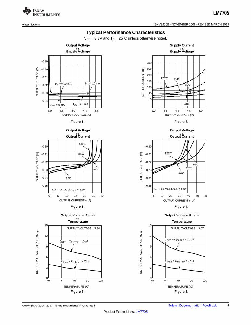
Typical Performance CharacteristicsVDD = 3.3V and TA = 25°C unless otherwise noted.
Output Voltage Supply Currentvs. vs.
Supply Voltage Supply Voltage
Figure 1. Figure 2.
Output Voltage Output Voltagevs. vs.
Output Current Output Current
Figure 3. Figure 4.
Output Voltage Ripple Output Voltage Ripplevs. vs.
Temperature Temperature
Figure 5. Figure 6.
Copyright © 2008–2013, Texas Instruments Incorporated Submit Documentation Feedback 5
Product Folder Links: LM7705
EN
AB
LE V
OLT
AG
E
TURN ON TIME (200 és/DIV)
OU
TP
UT
VO
LTA
GE
(0.
2V/D
IV)
ENABLE PULSE
0 mA5 mA
10 mA 20 mA
SUPPLY VOLTAGE = 3.3V
0V
0V
EN
AB
LE V
OLT
AG
E
TURN ON TIME (100 és/DIV)
OU
TP
UT
VO
LTA
GE
(0.
2V/D
IV)
ENABLE PULSE
0 mA
5 mA
10 mA
20 mA
0V
0V
SUPPLY VOLTAGE = 5.0V
OUTPUT CURRENT (mA)
CU
RR
EN
T C
ON
VE
RS
ION
EF
FIC
IEC
Y (
%)
110
105
100
95
90
85
80
0 4 8 12 16 20
-40°C
125°C
25°C 85°C
SUPPLY VOLTAGE = 3.3V
OUTPUT CURRENT (mA)
CU
RR
EN
T C
ON
VE
RS
ION
EF
FIC
IEC
Y (
%)
110
105
100
95
90
85
80
0 4 8 12 16 20
-40°C
125°C25°C85°C
SUPPLY VOLTAGE = 5.0V
OUTPUT CURRENT (mA)
SU
PP
LY C
UR
RE
NT
(mA
)
20
16
12
8
4
0
0 4 8 12 16 20
-40°C
125°C
25°C
85°C
SUPPLY VOLTAGE = 3.3V
OUTPUT CURRENT (mA)
SU
PP
LY C
UR
RE
NT
(m
A)
20
16
12
8
4
0
0 4 8 12 16 20
-40°C
125°C
25°C
85°C
SUPPLY VOLTAGE = 5.0V
LM7705
SNVS420B –NOVEMBER 2008–REVISED MARCH 2013 www.ti.com
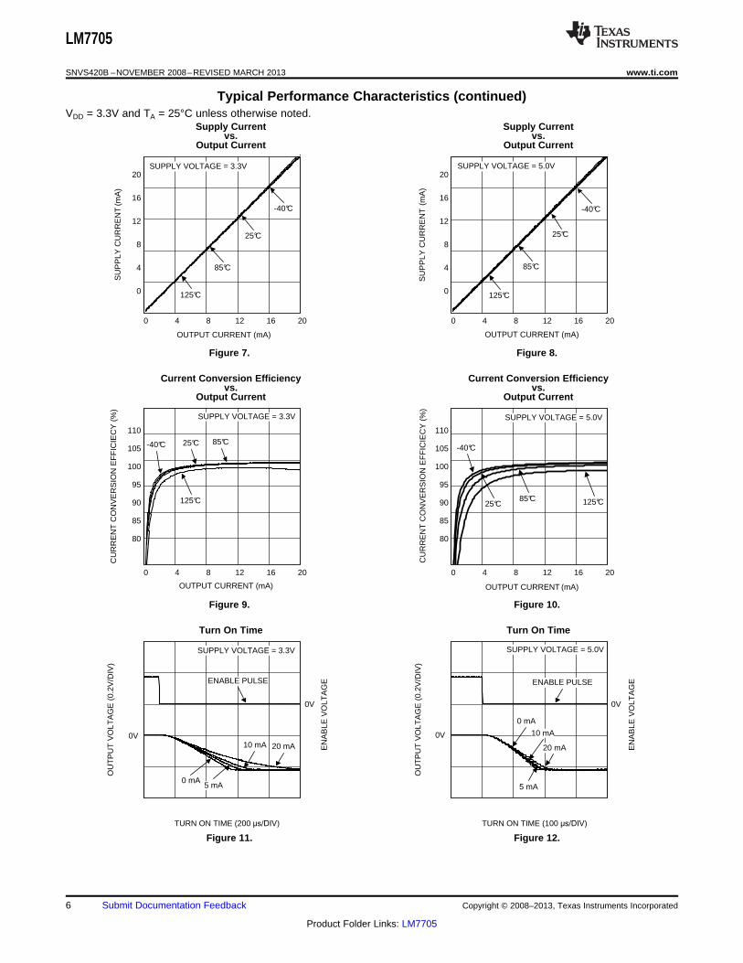
Typical Performance Characteristics (continued)VDD = 3.3V and TA = 25°C unless otherwise noted.
Supply Current Supply Currentvs. vs.
Output Current Output Current
Figure 7. Figure 8.
Current Conversion Efficiency Current Conversion Efficiencyvs. vs.
Output Current Output Current
Figure 9. Figure 10.
Turn On Time Turn On Time
Figure 11. Figure 12.
6 Submit Documentation Feedback Copyright © 2008–2013, Texas Instruments Incorporated
Product Folder Links: LM7705
OU
TP
UT
CU
RR
EN
T (
mA
)
TIME (20 us/DIV)
OU
TP
UT
VO
LTA
GE
(V
)
-0.210
-0.218
-0.226
-0.234
-0.242
-0.250
40
30
20
10
0
-10OUTPUT CURRENT
+25°C
+85/+125°C
-40°C
SUPPLY VOLTAGE = 3.3VO
UT
PU
T C
UR
RE
NT
(m
A)
TIME (20 us/DIV)
OU
TP
UT
VO
LTA
GE
(V
)
-0.210
-0.218
-0.226
-0.234
-0.242
-0.250
40
30
20
10
0
-10OUTPUT CURRENT
+25°C
+85/+125°C
-40°C
SUPPLY VOLTAGE = 5V
OU
TP
UT
CU
RR
EN
T (
mA
)
TIME (20 us/DIV)
OU
TP
UT
VO
LTA
GE
(V
)
-0.210
-0.218
-0.226
-0.234
-0.242
-0.250
40
30
20
10
0
-10
OUTPUT CURRENT
+25°C +85/+125°C
-40°C SUPPLY VOLTAGE = 3.3V
OU
TP
UT
CU
RR
EN
T (
mA
)
TIME (20 us/DIV)
OU
TP
UT
VO
LTA
GE
(V
)
-0.210
-0.218
-0.226
-0.234
-0.242
-0.250
40
30
20
10
0
-10
OUTPUT CURRENT
+25°C +85/+125°C
-40°C SUPPLY VOLTAGE = 5V
TEMPERATURE (°C)
LOA
D R
EG
ULA
TIO
N (
%/m
A)
0.4
0.3
0.2
0.1
0.0
-40 0 40 80 120
SUPPLY VOLTAGE = 3.3V
TEMPERATURE (°C)
LOA
D R
EG
ULA
TIO
N (
%/m
A)
0.4
0.3
0.2
0.1
0.0
-40 0 40 80 120
SUPPLY VOLTAGE = 5.0V
LM7705
www.ti.com SNVS420B –NOVEMBER 2008–REVISED MARCH 2013
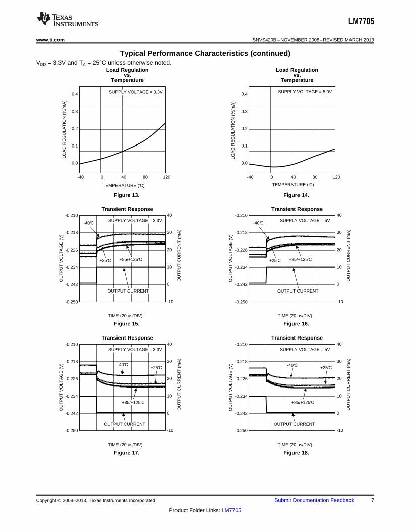
Typical Performance Characteristics (continued)VDD = 3.3V and TA = 25°C unless otherwise noted.
Load Regulation Load Regulationvs. vs.
Temperature Temperature
Figure 13. Figure 14.
Transient Response Transient Response
Figure 15. Figure 16.
Transient Response Transient Response
Figure 17. Figure 18.
Copyright © 2008–2013, Texas Instruments Incorporated Submit Documentation Feedback 7
Product Folder Links: LM7705
TEMPERATURE (°C)
OS
CIL
LAT
OR
FR
EQ
UE
NC
Y (
kHz)
100
95
90
85
80
75
70-40 0 40 80 120
SUPPLY VOLTAGE = 3.3V
SUPPLY VOLTAGE = 5V
SHUTDOWN VOLTAGE (V)
OU
TP
UT
VO
LTA
GE
(V
)
0
-0.05
-0.10
-0.15
-0.20
-0.25
0 1 2 3 4 5
SUPPLYVOLTAGE = 5V
SUPPLYVOLTAGE = 3.3V
SHUTDOWN VOLTAGE (V)
SU
PP
LY C
UR
RE
NT
(éA)
300
250
200
150
100
50
00 1 2 3 4 5
SUPPLY VOLTAGE = 5V
SUPPLY VOLTAGE = 3.3V
LM7705
SNVS420B –NOVEMBER 2008–REVISED MARCH 2013 www.ti.com
Typical Performance Characteristics (continued)VDD = 3.3V and TA = 25°C unless otherwise noted.
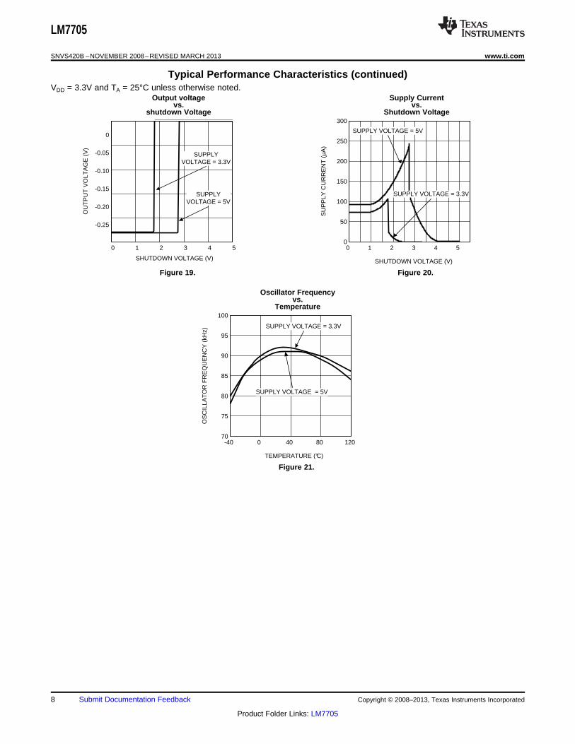
Output voltage Supply Currentvs. vs.
shutdown Voltage Shutdown Voltage
Figure 19. Figure 20.
Oscillator Frequencyvs.
Temperature
Figure 21.
8 Submit Documentation Feedback Copyright © 2008–2013, Texas Instruments Incorporated
Product Folder Links: LM7705
POWERSUPPLY
PREREGULATOR
LOADCHARGE
PUMPPOST
REGULATOR
LM7705
V+
OSCILLATOR
CFLY
OUT=V-
CRES
CAP+
CAP-
S2
S1
S4
S3
Ó1 Ó2
LM7705
www.ti.com SNVS420B –NOVEMBER 2008–REVISED MARCH 2013
APPLICATION INFORMATION
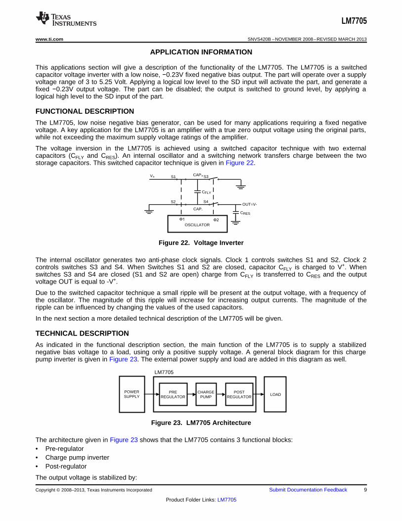
This applications section will give a description of the functionality of the LM7705. The LM7705 is a switchedcapacitor voltage inverter with a low noise, −0.23V fixed negative bias output. The part will operate over a supplyvoltage range of 3 to 5.25 Volt. Applying a logical low level to the SD input will activate the part, and generate afixed −0.23V output voltage. The part can be disabled; the output is switched to ground level, by applying alogical high level to the SD input of the part.
FUNCTIONAL DESCRIPTION
The LM7705, low noise negative bias generator, can be used for many applications requiring a fixed negativevoltage. A key application for the LM7705 is an amplifier with a true zero output voltage using the original parts,while not exceeding the maximum supply voltage ratings of the amplifier.
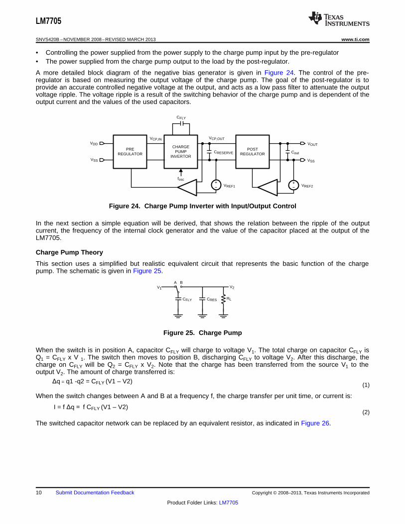
The voltage inversion in the LM7705 is achieved using a switched capacitor technique with two externalcapacitors (CFLY and CRES). An internal oscillator and a switching network transfers charge between the twostorage capacitors. This switched capacitor technique is given in Figure 22.
Figure 22. Voltage Inverter
The internal oscillator generates two anti-phase clock signals. Clock 1 controls switches S1 and S2. Clock 2controls switches S3 and S4. When Switches S1 and S2 are closed, capacitor CFLY is charged to V+. Whenswitches S3 and S4 are closed (S1 and S2 are open) charge from CFLY is transferred to CRES and the outputvoltage OUT is equal to -V+.
Due to the switched capacitor technique a small ripple will be present at the output voltage, with a frequency ofthe oscillator. The magnitude of this ripple will increase for increasing output currents. The magnitude of theripple can be influenced by changing the values of the used capacitors.
In the next section a more detailed technical description of the LM7705 will be given.
TECHNICAL DESCRIPTION
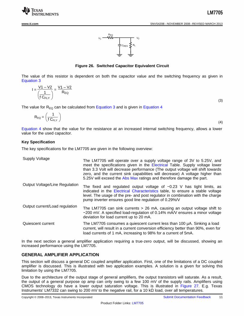
As indicated in the functional description section, the main function of the LM7705 is to supply a stabilizednegative bias voltage to a load, using only a positive supply voltage. A general block diagram for this chargepump inverter is given in Figure 23. The external power supply and load are added in this diagram as well.
Figure 23. LM7705 Architecture
The architecture given in Figure 23 shows that the LM7705 contains 3 functional blocks:• Pre-regulator• Charge pump inverter• Post-regulator
The output voltage is stabilized by:
Copyright © 2008–2013, Texas Instruments Incorporated Submit Documentation Feedback 9
Product Folder Links: LM7705
I = f Âq = f CFLY (V1 ± V2)
Âq = q1 -q2 = CFLY (V1 ± V2)
V1 V2
CRES RLCFLY
BA
CFLY
CHARGE PUMP
INVERTORCRESERVE
VREF1
PRE REGULATOR
VCP,IN
fosc
VOUT
VCP,OUT
POSTREGULATOR Cout
VDD
VSS VSS
VREF2
LM7705
SNVS420B –NOVEMBER 2008–REVISED MARCH 2013 www.ti.com
• Controlling the power supplied from the power supply to the charge pump input by the pre-regulator• The power supplied from the charge pump output to the load by the post-regulator.
A more detailed block diagram of the negative bias generator is given in Figure 24. The control of the pre-regulator is based on measuring the output voltage of the charge pump. The goal of the post-regulator is toprovide an accurate controlled negative voltage at the output, and acts as a low pass filter to attenuate the outputvoltage ripple. The voltage ripple is a result of the switching behavior of the charge pump and is dependent of theoutput current and the values of the used capacitors.
Figure 24. Charge Pump Inverter with Input/Output Control
In the next section a simple equation will be derived, that shows the relation between the ripple of the outputcurrent, the frequency of the internal clock generator and the value of the capacitor placed at the output of theLM7705.
Charge Pump Theory
This section uses a simplified but realistic equivalent circuit that represents the basic function of the chargepump. The schematic is given in Figure 25.
Figure 25. Charge Pump
When the switch is in position A, capacitor CFLY will charge to voltage V1. The total charge on capacitor CFLY isQ1 = CFLY x V 1. The switch then moves to position B, discharging CFLY to voltage V2. After this discharge, thecharge on CFLY will be Q2 = CFLY x V2. Note that the charge has been transferred from the source V1 to theoutput V2. The amount of charge transferred is:
(1)
When the switch changes between A and B at a frequency f, the charge transfer per unit time, or current is:
(2)
The switched capacitor network can be replaced by an equivalent resistor, as indicated in Figure 26.
10 Submit Documentation Feedback Copyright © 2008–2013, Texas Instruments Incorporated
Product Folder Links: LM7705
REQ =1
f CFLY ¹·
©§
I = REQ1
f CFLY ¹·
©§
V1 ± V2 V1 ± V2=
V1 V2
RL
REQ
CRES
LM7705
www.ti.com SNVS420B –NOVEMBER 2008–REVISED MARCH 2013
Figure 26. Switched Capacitor Equivalent Circuit
The value of this resistor is dependent on both the capacitor value and the switching frequency as given inEquation 3
(3)
The value for REQ can be calculated from Equation 3 and is given in Equation 4
(4)
Equation 4 show that the value for the resistance at an increased internal switching frequency, allows a lowervalue for the used capacitor.
Key Specification
The key specifications for the LM7705 are given in the following overview:
Supply Voltage The LM7705 will operate over a supply voltage range of 3V to 5.25V, andmeet the specifications given in the Electrical Table. Supply voltage lowerthan 3.3 Volt will decrease performance (The output voltage will shift towardszero, and the current sink capabilities will decrease) A voltage higher than5.25V will exceed the Abs Max ratings and therefore damage the part.
Output Voltage/Line Regulation The fixed and regulated output voltage of −0.23 V has tight limits, asindicated in the Electrical Characteristics table, to ensure a stable voltagelevel. The usage of the pre- and post regulator in combination with the chargepump inverter ensures good line regulation of 0.29%/V
Output current/Load regulation The LM7705 can sink currents > 26 mA, causing an output voltage shift to−200 mV. A specified load-regulation of 0.14% mA/V ensures a minor voltagedeviation for load current up to 20 mA.
Quiescent current The LM7705 consumes a quiescent current less than 100 µA. Sinking a loadcurrent, will result in a current conversion efficiency better than 90%, even forload currents of 1 mA, increasing to 98% for a current of 5mA.
In the next section a general amplifier application requiring a true-zero output, will be discussed, showing anincreased performance using the LM7705.
GENERAL AMPLIFIER APPLICATION
This section will discuss a general DC coupled amplifier application. First, one of the limitations of a DC coupledamplifier is discussed. This is illustrated with two application examples. A solution is a given for solving thislimitation by using the LM7705.
Due to the architecture of the output stage of general amplifiers, the output transistors will saturate. As a result,the output of a general purpose op amp can only swing to a few 100 mV of the supply rails. Amplifiers usingCMOS technology do have a lower output saturation voltage. This is illustrated in Figure 27. E.g. TexasInstruments' LM7332 can swing to 200 mV to the negative rail, for a 10 kΩ load, over all temperatures.
Copyright © 2008–2013, Texas Instruments Incorporated Submit Documentation Feedback 11
Product Folder Links: LM7705
+V
ADC
RF1
-
+
VREF
RG1
GAIN = 50x
ADC122S021LMP7701
SENSOR
VIN
+V
-
+
0V
VOUT
0V
VDSAT
INPUT VOLTAGE (V)O
UT
PU
T V
OLT
AG
E (
V)
V+
00 V+
VDSAT
OUTPUT SATURATION
LM7705
SNVS420B –NOVEMBER 2008–REVISED MARCH 2013 www.ti.com
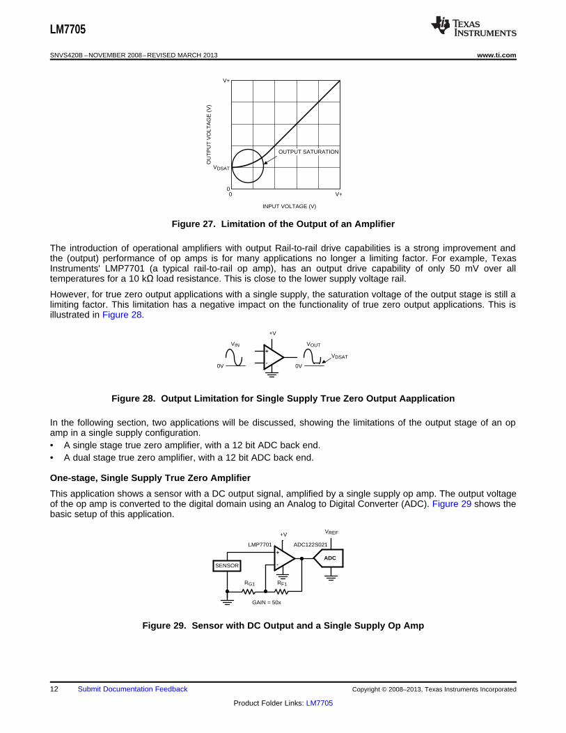
Figure 27. Limitation of the Output of an Amplifier
The introduction of operational amplifiers with output Rail-to-rail drive capabilities is a strong improvement andthe (output) performance of op amps is for many applications no longer a limiting factor. For example, TexasInstruments' LMP7701 (a typical rail-to-rail op amp), has an output drive capability of only 50 mV over alltemperatures for a 10 kΩ load resistance. This is close to the lower supply voltage rail.
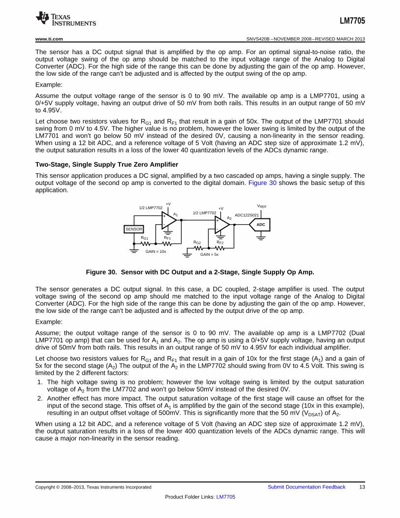
However, for true zero output applications with a single supply, the saturation voltage of the output stage is still alimiting factor. This limitation has a negative impact on the functionality of true zero output applications. This isillustrated in Figure 28.
Figure 28. Output Limitation for Single Supply True Zero Output Aapplication
In the following section, two applications will be discussed, showing the limitations of the output stage of an opamp in a single supply configuration.• A single stage true zero amplifier, with a 12 bit ADC back end.• A dual stage true zero amplifier, with a 12 bit ADC back end.
One-stage, Single Supply True Zero Amplifier
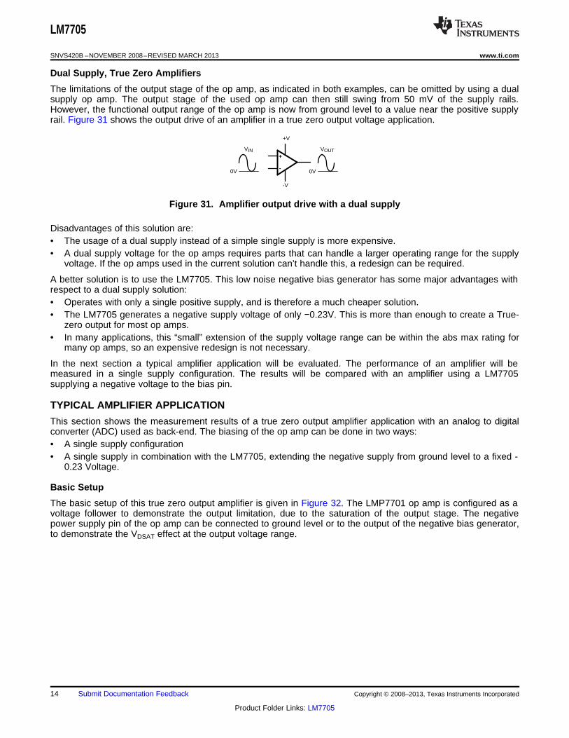
This application shows a sensor with a DC output signal, amplified by a single supply op amp. The output voltageof the op amp is converted to the digital domain using an Analog to Digital Converter (ADC). Figure 29 shows thebasic setup of this application.
Figure 29. Sensor with DC Output and a Single Supply Op Amp
12 Submit Documentation Feedback Copyright © 2008–2013, Texas Instruments Incorporated
Product Folder Links: LM7705
+V
RF1
-
+
RG1RF2
-
+
RG2
A1A2
ADC
VREF+V
GAIN = 10x GAIN = 5x
ADC122S0211/2 LMP77021/2 LMP7702
SENSOR
LM7705
www.ti.com SNVS420B –NOVEMBER 2008–REVISED MARCH 2013
The sensor has a DC output signal that is amplified by the op amp. For an optimal signal-to-noise ratio, theoutput voltage swing of the op amp should be matched to the input voltage range of the Analog to DigitalConverter (ADC). For the high side of the range this can be done by adjusting the gain of the op amp. However,the low side of the range can’t be adjusted and is affected by the output swing of the op amp.
Example:
Assume the output voltage range of the sensor is 0 to 90 mV. The available op amp is a LMP7701, using a0/+5V supply voltage, having an output drive of 50 mV from both rails. This results in an output range of 50 mVto 4.95V.
Let choose two resistors values for RG1 and RF1 that result in a gain of 50x. The output of the LMP7701 shouldswing from 0 mV to 4.5V. The higher value is no problem, however the lower swing is limited by the output of theLM7701 and won’t go below 50 mV instead of the desired 0V, causing a non-linearity in the sensor reading.When using a 12 bit ADC, and a reference voltage of 5 Volt (having an ADC step size of approximate 1.2 mV),the output saturation results in a loss of the lower 40 quantization levels of the ADCs dynamic range.
Two-Stage, Single Supply True Zero Amplifier
This sensor application produces a DC signal, amplified by a two cascaded op amps, having a single supply. Theoutput voltage of the second op amp is converted to the digital domain. Figure 30 shows the basic setup of thisapplication.
Figure 30. Sensor with DC Output and a 2-Stage, Single Supply Op Amp.
The sensor generates a DC output signal. In this case, a DC coupled, 2-stage amplifier is used. The outputvoltage swing of the second op amp should me matched to the input voltage range of the Analog to DigitalConverter (ADC). For the high side of the range this can be done by adjusting the gain of the op amp. However,the low side of the range can’t be adjusted and is affected by the output drive of the op amp.
Example:
Assume; the output voltage range of the sensor is 0 to 90 mV. The available op amp is a LMP7702 (DualLMP7701 op amp) that can be used for A1 and A2. The op amp is using a 0/+5V supply voltage, having an outputdrive of 50mV from both rails. This results in an output range of 50 mV to 4.95V for each individual amplifier.
Let choose two resistors values for RG1 and RF1 that result in a gain of 10x for the first stage (A1) and a gain of5x for the second stage (A2) The output of the A2 in the LMP7702 should swing from 0V to 4.5 Volt. This swing islimited by the 2 different factors:1. The high voltage swing is no problem; however the low voltage swing is limited by the output saturation
voltage of A2 from the LM7702 and won’t go below 50mV instead of the desired 0V.2. Another effect has more impact. The output saturation voltage of the first stage will cause an offset for the
input of the second stage. This offset of A1 is amplified by the gain of the second stage (10x in this example),resulting in an output offset voltage of 500mV. This is significantly more that the 50 mV (VDSAT) of A2.
When using a 12 bit ADC, and a reference voltage of 5 Volt (having an ADC step size of approximate 1.2 mV),the output saturation results in a loss of the lower 400 quantization levels of the ADCs dynamic range. This willcause a major non-linearity in the sensor reading.
Copyright © 2008–2013, Texas Instruments Incorporated Submit Documentation Feedback 13
Product Folder Links: LM7705
VIN
+V
-
+
0V
VOUT
0V
-V
LM7705
SNVS420B –NOVEMBER 2008–REVISED MARCH 2013 www.ti.com
Dual Supply, True Zero Amplifiers
The limitations of the output stage of the op amp, as indicated in both examples, can be omitted by using a dualsupply op amp. The output stage of the used op amp can then still swing from 50 mV of the supply rails.However, the functional output range of the op amp is now from ground level to a value near the positive supplyrail. Figure 31 shows the output drive of an amplifier in a true zero output voltage application.
Figure 31. Amplifier output drive with a dual supply
Disadvantages of this solution are:• The usage of a dual supply instead of a simple single supply is more expensive.• A dual supply voltage for the op amps requires parts that can handle a larger operating range for the supply
voltage. If the op amps used in the current solution can’t handle this, a redesign can be required.
A better solution is to use the LM7705. This low noise negative bias generator has some major advantages withrespect to a dual supply solution:• Operates with only a single positive supply, and is therefore a much cheaper solution.• The LM7705 generates a negative supply voltage of only −0.23V. This is more than enough to create a True-
zero output for most op amps.• In many applications, this “small” extension of the supply voltage range can be within the abs max rating for
many op amps, so an expensive redesign is not necessary.
In the next section a typical amplifier application will be evaluated. The performance of an amplifier will bemeasured in a single supply configuration. The results will be compared with an amplifier using a LM7705supplying a negative voltage to the bias pin.
TYPICAL AMPLIFIER APPLICATION
This section shows the measurement results of a true zero output amplifier application with an analog to digitalconverter (ADC) used as back-end. The biasing of the op amp can be done in two ways:• A single supply configuration• A single supply in combination with the LM7705, extending the negative supply from ground level to a fixed -
0.23 Voltage.
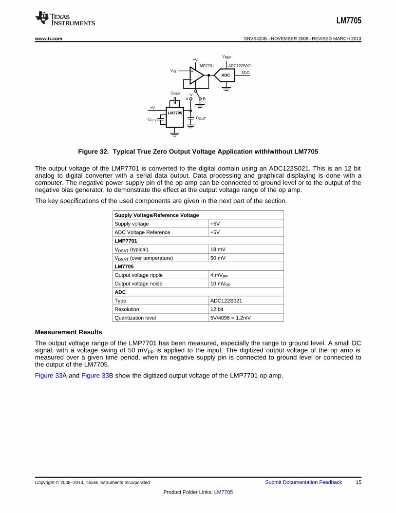
Basic Setup
The basic setup of this true zero output amplifier is given in Figure 32. The LMP7701 op amp is configured as avoltage follower to demonstrate the output limitation, due to the saturation of the output stage. The negativepower supply pin of the op amp can be connected to ground level or to the output of the negative bias generator,to demonstrate the VDSAT effect at the output voltage range.
14 Submit Documentation Feedback Copyright © 2008–2013, Texas Instruments Incorporated
Product Folder Links: LM7705
VIN
+V
ADC-
+
VREF
LMP7701 ADC122S021
SDO
LM7705+V
COUT
CRES
CFLY
BA-V
LM7705
www.ti.com SNVS420B –NOVEMBER 2008–REVISED MARCH 2013
Figure 32. Typical True Zero Output Voltage Application with/without LM7705
The output voltage of the LMP7701 is converted to the digital domain using an ADC122S021. This is an 12 bitanalog to digital converter with a serial data output. Data processing and graphical displaying is done with acomputer. The negative power supply pin of the op amp can be connected to ground level or to the output of thenegative bias generator, to demonstrate the effect at the output voltage range of the op amp.
The key specifications of the used components are given in the next part of the section.
Supply Voltage/Reference Voltage
Supply voltage +5V
ADC Voltage Reference +5V
LMP7701
VDSAT (typical) 18 mV
VDSAT (over temperature) 50 mV
LM7705
Output voltage ripple 4 mVPP
Output voltage noise 10 mVPP
ADC
Type ADC122S021
Resolution 12 bit
Quantization level 5V/4096 = 1.2mV
Measurement Results
The output voltage range of the LMP7701 has been measured, especially the range to ground level. A small DCsignal, with a voltage swing of 50 mVPP is applied to the input. The digitized output voltage of the op amp ismeasured over a given time period, when its negative supply pin is connected to ground level or connected tothe output of the LM7705.
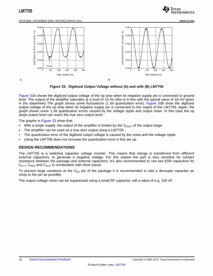
Figure 33A and Figure 33B show the digitized output voltage of the LMP7701 op amp.
Copyright © 2008–2013, Texas Instruments Incorporated Submit Documentation Feedback 15
Product Folder Links: LM7705
TIME (SAMPLES)
DIG
ITIZ
ED
OU
TP
UT
VO
LTA
GE
(`V
)
0.050
0.040
0.030
0.020
0.010
0.0000 80 160 240 320 400
VDSAT
TIME (SAMPLES)
DIG
ITIZ
ED
OU
TP
UT
VO
LTA
GE
(V
)
0.050
0.040
0.030
0.020
0.010
0.0000 80 160 240 320 400
LM7705
SNVS420B –NOVEMBER 2008–REVISED MARCH 2013 www.ti.com
A B
Figure 33. Digitized Output Voltage without (A) and with (B) LM7705
Figure 33A shows the digitized output voltage of the op amp when its negative supply pin is connected to groundlevel. The output of the amplifier saturates at a level of 14 mv (this is in line with the typical value of 18 mV givenin the datasheet) The graph shows some fluctuations (1 bit quantization error). Figure 33B show the digitizedoutput voltage of the op amp when its negative supply pin is connected to the output of the LM7705. Again, thegraph shows some 1 bit quantization errors caused by the voltage ripple and output noise. In this case the opamps output level can reach the true zero output level.
The graphs in Figure 33 show that:• With a single supply, the output of the amplifier is limited by the VDSAT of the output stage.• The amplifier can be used as a true zero output using a LM7705.• The quantization error of the digitized output voltage is caused by the noise and the voltage ripple.• Using the LM7705 does not increase the quantization error in this set up.
DESIGN RECOMMENDATIONS
The LM7705 is a switched capacitor voltage inverter. This means that charge is transferred from differentexternal capacitors, to generate a negative voltage. For this reason the part is very sensitive for contactresistance between the package and external capacitors. It’s also recommended to use low ESR capacitors forCFLY, CRES and COUT in combination with short traces.
To prevent large variations at the VDD pin of the package it is recommended to add a decouple capacitor asclose to the pin as possible.
The output voltage noise can be suppressed using a small RF capacitor, will a value of e.g. 100 nF.
16 Submit Documentation Feedback Copyright © 2008–2013, Texas Instruments Incorporated
Product Folder Links: LM7705
LM7705
www.ti.com SNVS420B –NOVEMBER 2008–REVISED MARCH 2013
REVISION HISTORY
Changes from Revision A (March 2013) to Revision B Page
• Changed layout of National Data Sheet to TI format .......................................................................................................... 16
Copyright © 2008–2013, Texas Instruments Incorporated Submit Documentation Feedback 17
Product Folder Links: LM7705
PACKAGE OPTION ADDENDUM
www.ti.com 11-Apr-2013
Addendum-Page 1
PACKAGING INFORMATION
Orderable Device Status(1)
Package Type PackageDrawing
Pins PackageQty
Eco Plan(2)
Lead/Ball Finish MSL Peak Temp(3)
Op Temp (°C) Top-Side Markings(4)
Samples
LM7705MM/NOPB ACTIVE VSSOP DGK 8 1000 Green (RoHS& no Sb/Br)
CU SN Level-1-260C-UNLIM -40 to 125 F26A
LM7705MME/NOPB ACTIVE VSSOP DGK 8 250 Green (RoHS& no Sb/Br)
CU SN Level-1-260C-UNLIM -40 to 125 F26A
LM7705MMX/NOPB ACTIVE VSSOP DGK 8 3500 Green (RoHS& no Sb/Br)
CU SN Level-1-260C-UNLIM -40 to 125 F26A
(1) The marketing status values are defined as follows:ACTIVE: Product device recommended for new designs.LIFEBUY: TI has announced that the device will be discontinued, and a lifetime-buy period is in effect.NRND: Not recommended for new designs. Device is in production to support existing customers, but TI does not recommend using this part in a new design.PREVIEW: Device has been announced but is not in production. Samples may or may not be available.OBSOLETE: TI has discontinued the production of the device.
(2) Eco Plan - The planned eco-friendly classification: Pb-Free (RoHS), Pb-Free (RoHS Exempt), or Green (RoHS & no Sb/Br) - please check http://www.ti.com/productcontent for the latest availabilityinformation and additional product content details.TBD: The Pb-Free/Green conversion plan has not been defined.Pb-Free (RoHS): TI's terms "Lead-Free" or "Pb-Free" mean semiconductor products that are compatible with the current RoHS requirements for all 6 substances, including the requirement thatlead not exceed 0.1% by weight in homogeneous materials. Where designed to be soldered at high temperatures, TI Pb-Free products are suitable for use in specified lead-free processes.Pb-Free (RoHS Exempt): This component has a RoHS exemption for either 1) lead-based flip-chip solder bumps used between the die and package, or 2) lead-based die adhesive used betweenthe die and leadframe. The component is otherwise considered Pb-Free (RoHS compatible) as defined above.Green (RoHS & no Sb/Br): TI defines "Green" to mean Pb-Free (RoHS compatible), and free of Bromine (Br) and Antimony (Sb) based flame retardants (Br or Sb do not exceed 0.1% by weightin homogeneous material)
(3) MSL, Peak Temp. -- The Moisture Sensitivity Level rating according to the JEDEC industry standard classifications, and peak solder temperature.
(4) Multiple Top-Side Markings will be inside parentheses. Only one Top-Side Marking contained in parentheses and separated by a "~" will appear on a device. If a line is indented then it is acontinuation of the previous line and the two combined represent the entire Top-Side Marking for that device.
Important Information and Disclaimer:The information provided on this page represents TI's knowledge and belief as of the date that it is provided. TI bases its knowledge and belief on informationprovided by third parties, and makes no representation or warranty as to the accuracy of such information. Efforts are underway to better integrate information from third parties. TI has taken andcontinues to take reasonable steps to provide representative and accurate information but may not have conducted destructive testing or chemical analysis on incoming materials and chemicals.TI and TI suppliers consider certain information to be proprietary, and thus CAS numbers and other limited information may not be available for release.
In no event shall TI's liability arising out of such information exceed the total purchase price of the TI part(s) at issue in this document sold by TI to Customer on an annual basis.
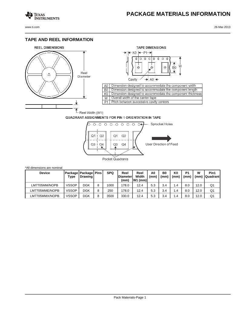
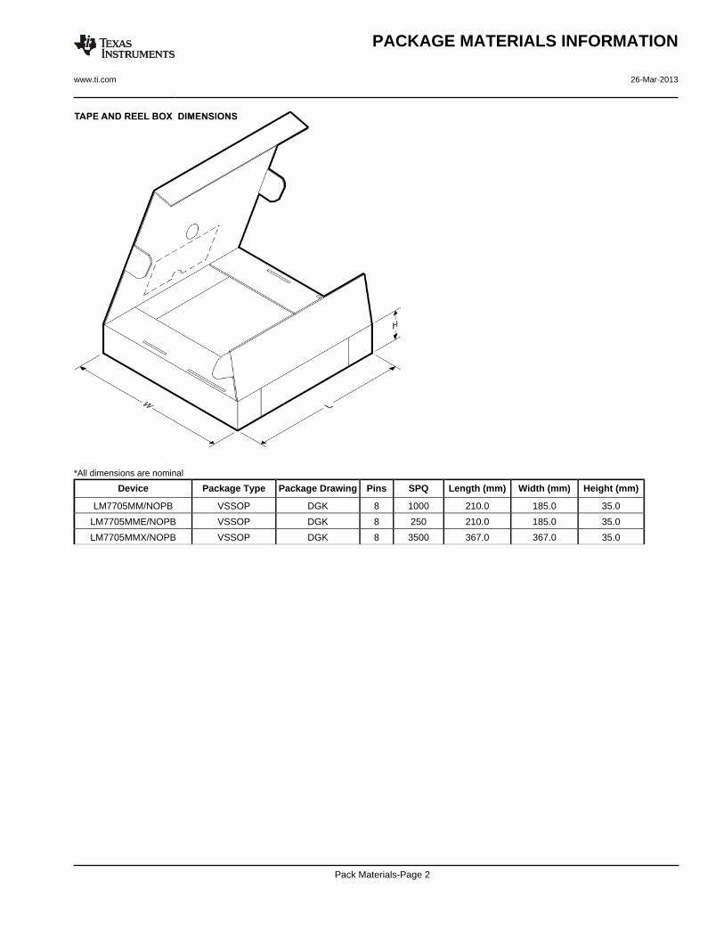
TAPE AND REEL INFORMATION
*All dimensions are nominal
Device PackageType
PackageDrawing
Pins SPQ ReelDiameter
(mm)
ReelWidth
W1 (mm)
A0(mm)
B0(mm)
K0(mm)
P1(mm)
W(mm)
Pin1Quadrant
LM7705MM/NOPB VSSOP DGK 8 1000 178.0 12.4 5.3 3.4 1.4 8.0 12.0 Q1
LM7705MME/NOPB VSSOP DGK 8 250 178.0 12.4 5.3 3.4 1.4 8.0 12.0 Q1
LM7705MMX/NOPB VSSOP DGK 8 3500 330.0 12.4 5.3 3.4 1.4 8.0 12.0 Q1
PACKAGE MATERIALS INFORMATION
www.ti.com 26-Mar-2013
Pack Materials-Page 1
*All dimensions are nominal
Device Package Type Package Drawing Pins SPQ Length (mm) Width (mm) Height (mm)
LM7705MM/NOPB VSSOP DGK 8 1000 210.0 185.0 35.0
LM7705MME/NOPB VSSOP DGK 8 250 210.0 185.0 35.0
LM7705MMX/NOPB VSSOP DGK 8 3500 367.0 367.0 35.0
PACKAGE MATERIALS INFORMATION
www.ti.com 26-Mar-2013
Pack Materials-Page 2
IMPORTANT NOTICE
Texas Instruments Incorporated and its subsidiaries (TI) reserve the right to make corrections, enhancements, improvements and otherchanges to its semiconductor products and services per JESD46, latest issue, and to discontinue any product or service per JESD48, latestissue. Buyers should obtain the latest relevant information before placing orders and should verify that such information is current andcomplete. All semiconductor products (also referred to herein as “components”) are sold subject to TI’s terms and conditions of salesupplied at the time of order acknowledgment.
TI warrants performance of its components to the specifications applicable at the time of sale, in accordance with the warranty in TI’s termsand conditions of sale of semiconductor products. Testing and other quality control techniques are used to the extent TI deems necessaryto support this warranty. Except where mandated by applicable law, testing of all parameters of each component is not necessarilyperformed.
TI assumes no liability for applications assistance or the design of Buyers’ products. Buyers are responsible for their products andapplications using TI components. To minimize the risks associated with Buyers’ products and applications, Buyers should provideadequate design and operating safeguards.
TI does not warrant or represent that any license, either express or implied, is granted under any patent right, copyright, mask work right, orother intellectual property right relating to any combination, machine, or process in which TI components or services are used. Informationpublished by TI regarding third-party products or services does not constitute a license to use such products or services or a warranty orendorsement thereof. Use of such information may require a license from a third party under the patents or other intellectual property of thethird party, or a license from TI under the patents or other intellectual property of TI.
Reproduction of significant portions of TI information in TI data books or data sheets is permissible only if reproduction is without alterationand is accompanied by all associated warranties, conditions, limitations, and notices. TI is not responsible or liable for such altereddocumentation. Information of third parties may be subject to additional restrictions.
Resale of TI components or services with statements different from or beyond the parameters stated by TI for that component or servicevoids all express and any implied warranties for the associated TI component or service and is an unfair and deceptive business practice.TI is not responsible or liable for any such statements.
Buyer acknowledges and agrees that it is solely responsible for compliance with all legal, regulatory and safety-related requirementsconcerning its products, and any use of TI components in its applications, notwithstanding any applications-related information or supportthat may be provided by TI. Buyer represents and agrees that it has all the necessary expertise to create and implement safeguards whichanticipate dangerous consequences of failures, monitor failures and their consequences, lessen the likelihood of failures that might causeharm and take appropriate remedial actions. Buyer will fully indemnify TI and its representatives against any damages arising out of the useof any TI components in safety-critical applications.
In some cases, TI components may be promoted specifically to facilitate safety-related applications. With such components, TI’s goal is tohelp enable customers to design and create their own end-product solutions that meet applicable functional safety standards andrequirements. Nonetheless, such components are subject to these terms.
No TI components are authorized for use in FDA Class III (or similar life-critical medical equipment) unless authorized officers of the partieshave executed a special agreement specifically governing such use.
Only those TI components which TI has specifically designated as military grade or “enhanced plastic” are designed and intended for use inmilitary/aerospace applications or environments. Buyer acknowledges and agrees that any military or aerospace use of TI componentswhich have not been so designated is solely at the Buyer's risk, and that Buyer is solely responsible for compliance with all legal andregulatory requirements in connection with such use.
TI has specifically designated certain components as meeting ISO/TS16949 requirements, mainly for automotive use. In any case of use ofnon-designated products, TI will not be responsible for any failure to meet ISO/TS16949.
Products Applications
Audio www.ti.com/audio Automotive and Transportation www.ti.com/automotive
Amplifiers amplifier.ti.com Communications and Telecom www.ti.com/communications
Data Converters dataconverter.ti.com Computers and Peripherals www.ti.com/computers
DLP® Products www.dlp.com Consumer Electronics www.ti.com/consumer-apps
DSP dsp.ti.com Energy and Lighting www.ti.com/energy
Clocks and Timers www.ti.com/clocks Industrial www.ti.com/industrial
Interface interface.ti.com Medical www.ti.com/medical
Logic logic.ti.com Security www.ti.com/security
Power Mgmt power.ti.com Space, Avionics and Defense www.ti.com/space-avionics-defense
Microcontrollers microcontroller.ti.com Video and Imaging www.ti.com/video
RFID www.ti-rfid.com
OMAP Applications Processors www.ti.com/omap TI E2E Community e2e.ti.com
Wireless Connectivity www.ti.com/wirelessconnectivity
Mailing Address: Texas Instruments, Post Office Box 655303, Dallas, Texas 75265Copyright © 2013, Texas Instruments Incorporated