Embed Size (px)
Citation preview
SLOS019E − SEPTEMBER 1988 − REVISED FEBRUARY 2005
1POST OFFICE BOX 655303 • DALLAS, TEXAS 75265
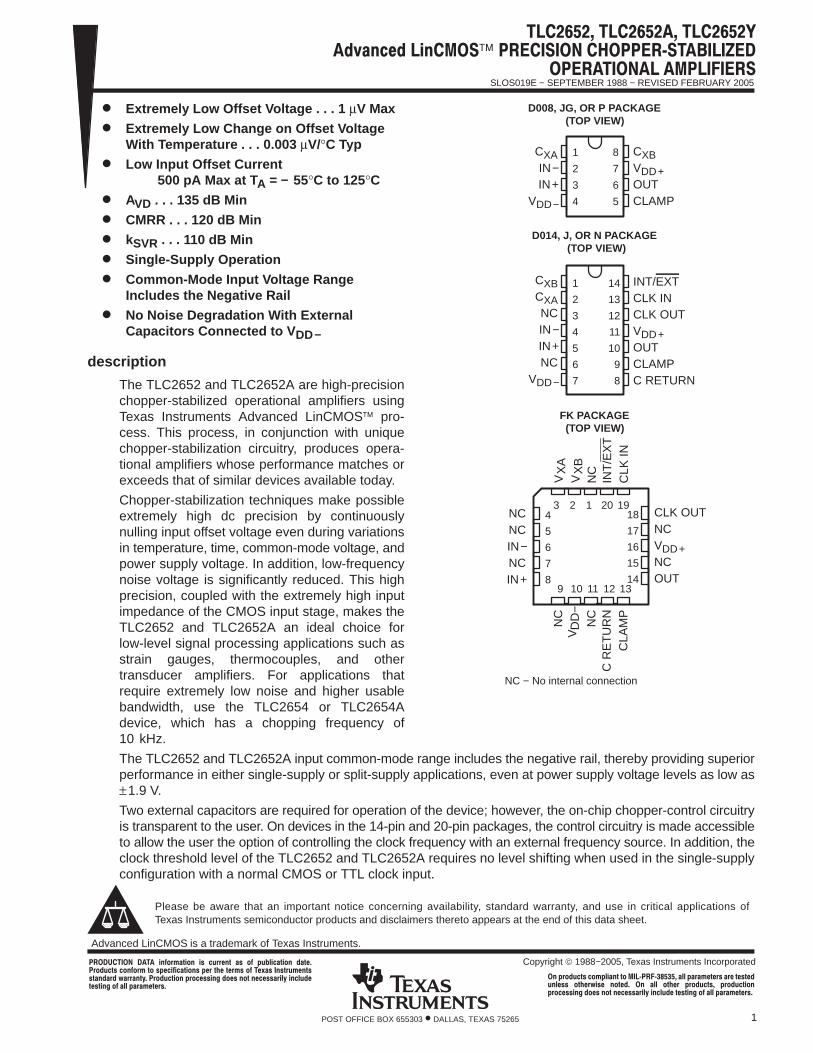
Extremely Low Offset Voltage . . . 1 µV Max
Extremely Low Change on Offset VoltageWith Temperature . . . 0.003 µV/°C Typ
Low Input Offset Current500 pA Max at T A = − 55°C to 125°C
AVD . . . 135 dB Min
CMRR . . . 120 dB Min
kSVR . . . 110 dB Min
Single-Supply Operation
Common-Mode Input Voltage RangeIncludes the Negative Rail
No Noise Degradation With ExternalCapacitors Connected to V DD−
description
The TLC2652 and TLC2652A are high-precisionchopper-stabilized operational amplifiers usingTexas Instruments Advanced LinCMOS pro-cess. This process, in conjunction with uniquechopper-stabilization circuitry, produces opera-tional amplifiers whose performance matches orexceeds that of similar devices available today.
Chopper-stabilization techniques make possibleextremely high dc precision by continuouslynulling input offset voltage even during variationsin temperature, time, common-mode voltage, andpower supply voltage. In addition, low-frequencynoise voltage is significantly reduced. This highprecision, coupled with the extremely high inputimpedance of the CMOS input stage, makes theTLC2652 and TLC2652A an ideal choice forlow-level signal processing applications such asstrain gauges, thermocouples, and othertransducer amplifiers. For applications thatrequire extremely low noise and higher usablebandwidth, use the TLC2654 or TLC2654Adevice, which has a chopping frequency of10 kHz.
The TLC2652 and TLC2652A input common-mode range includes the negative rail, thereby providing superiorperformance in either single-supply or split-supply applications, even at power supply voltage levels as low as±1.9 V.
Two external capacitors are required for operation of the device; however, the on-chip chopper-control circuitryis transparent to the user. On devices in the 14-pin and 20-pin packages, the control circuitry is made accessibleto allow the user the option of controlling the clock frequency with an external frequency source. In addition, theclock threshold level of the TLC2652 and TLC2652A requires no level shifting when used in the single-supplyconfiguration with a normal CMOS or TTL clock input.
Copyright 1988−2005, Texas Instruments Incorporated !"#$%" & '## % & "! (')*%" %+#"'%& " !"#$ %" &(!%" & (# %, %#$& "! -& &%#'$ %&&% # .## %/+ #"'%" (#"&& 0 "& "% &&#*/ *'%&% 0 "! ** (#$%#&+
Please be aware that an important notice concerning availability, standard warranty, and use in critical applications ofTexas Instruments semiconductor products and disclaimers thereto appears at the end of this data sheet.
Advanced LinCMOS is a trademark of Texas Instruments.
1
2
3
4
8
7
6
5
CXBVDD+OUTCLAMP
D008, JG, OR P PACKAGE
NC − No internal connection
1
2
3
4
5
6
7
14
13
12
11
10
9
8
INT/EXTCLK INCLK OUTVDD+OUTCLAMPC RETURN
D014, J, OR N PACKAGE(TOP VIEW)
3 2 1 20 19
9 10 11 12 13
4
5
6
7
8
18
17
16
15
14
CLK OUTNCVDD+NCOUT
FK PACKAGE(TOP VIEW)
INT
/EX
TN
C
CLA
MP
CLK
IN
NC
NC
XA
V
C R
ET
UR
N
XB
VD
D−
V
(TOP VIEW)
NCNCIN−NCIN+
CXBCXANCIN−IN+NC
VDD−
CXAIN−IN+
VDD−
(#"'%& "$(* % %" 121 ** (#$%#& # %&%' *&& "%,#.& "%+ ** "%,# (#"'%& (#"'%" (#"&& 0 "& "% &&#*/ *' %&% 0 "! ** (#$%#&+
SLOS019E − SEPTEMBER 1988 − REVISED FEBRUARY 2005
2 POST OFFICE BOX 655303 • DALLAS, TEXAS 75265
description (continued)
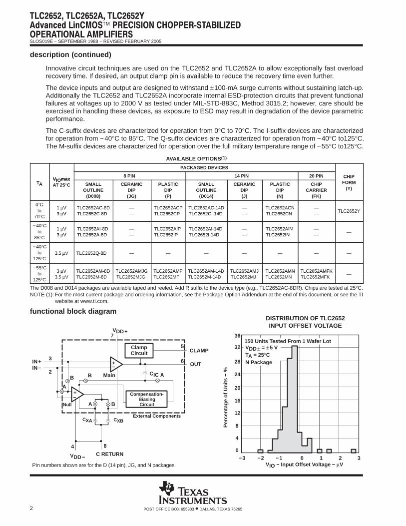
Innovative circuit techniques are used on the TLC2652 and TLC2652A to allow exceptionally fast overloadrecovery time. If desired, an output clamp pin is available to reduce the recovery time even further.
The device inputs and output are designed to withstand ±100-mA surge currents without sustaining latch-up.Additionally the TLC2652 and TLC2652A incorporate internal ESD-protection circuits that prevent functionalfailures at voltages up to 2000 V as tested under MIL-STD-883C, Method 3015.2; however, care should beexercised in handling these devices, as exposure to ESD may result in degradation of the device parametricperformance.
The C-suffix devices are characterized for operation from 0°C to 70°C. The I-suffix devices are characterizedfor operation from −40°C to 85°C. The Q-suffix devices are characterized for operation from −40°C to125°C.The M-suffix devices are characterized for operation over the full military temperature range of −55°C to125°C.
AVAILABLE OPTIONS (1)
PACKAGED DEVICES
VIOmax8 PIN 14 PIN 20 PIN CHIP
FORMTAVIOmaxAT 25°C SMALL
OUTLINE(D008)
CERAMICDIP(JG)
PLASTICDIP(P)
SMALLOUTLINE
(D014)
CERAMICDIP(J)
PLASTICDIP(N)
CHIPCARRIER
(FK)
CHIPFORM
(Y)
0°C1 µV TLC2652AC-8D — TLC2652ACP TLC2652AC-14D — TLC2652ACN —
0 Cto
70 C
1 µV3 µV
TLC2652AC-8DTLC2652C-8D
——
TLC2652ACPTLC2652CP
TLC2652AC-14DTLC2652C- 14D
——
TLC2652ACNTLC2652CN
——
TLC2652Yto70°C 3 µV TLC2652C-8D — TLC2652CP TLC2652C- 14D — TLC2652CN —
TLC2652Y
−40°C1 µV TLC2652AI-8D — TLC2652AIP TLC2652AI-14D — TLC2652AIN —
−40 Cto
85 C
1 µV3 µV
TLC2652AI-8DTLC2652A-8D
——
TLC2652AIPTLC2652IP
TLC2652AI-14DTLC2652I-14D
——
TLC2652AINTLC2652IN
——
—to85°C 3 µV TLC2652A-8D — TLC2652IP TLC2652I-14D — TLC2652IN —
—
−40°C−40 Cto
125 C3.5 µV TLC2652Q-8D — — — — — — —to
125°C3.5 µV TLC2652Q-8D — — — — — — —
−55°Cto
3 µV TLC2652AM-8D TLC2652AMJG TLC2652AMP TLC2652AM-14D TLC2652AMJ TLC2652AMN TLC2652AMFK—to
125°C
3 µV3.5 µV
TLC2652AM-8DTLC2652M-8D
TLC2652AMJGTLC2652MJG
TLC2652AMPTLC2652MP
TLC2652AM-14DTLC2652M-14D
TLC2652AMJTLC2652MJ
TLC2652AMNTLC2652MN
TLC2652AMFKTLC2652MFK
—
The D008 and D014 packages are available taped and reeled. Add R suffix to the device type (e.g., TLC2652AC-8DR). Chips are tested at 25°C.NOTE (1): For the most current package and ordering information, see the Package Option Addendum at the end of this document, or see the TI
website at www.ti.com.
functional block diagram
ClampCircuit CLAMP
OUT
C RETURNVDD−
Compensation-BiasingCircuit
VDD+
A
B B A
IN+IN−
CXA CXBExternal Components
Null
Main
+−
+−
A B
DISTRIBUTION OF TLC2652INPUT OFFSET VOLTAGE
Per
cent
age
of U
nits
− %
VIO − Input Offset Voltage − µV−3 −2 −1 0 1 2 3
0
4
8
12
16
20
24
28
32
36150 Units Tested From 1 Wafer LotVDD± = ±5 VTA = 25°CN Package
CIC
5
4
2
3 6
7
8
Pin numbers shown are for the D (14 pin), JG, and N packages.
SLOS019E − SEPTEMBER 1988 − REVISED FEBRUARY 2005
3POST OFFICE BOX 655303 • DALLAS, TEXAS 75265
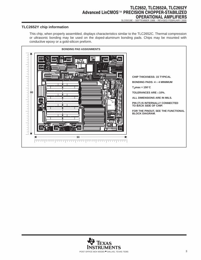
TLC2652Y chip information
This chip, when properly assembled, displays characteristics similar to the TLC2652C. Thermal compressionor ultrasonic bonding may be used on the doped-aluminum bonding pads. Chips may be mounted withconductive epoxy or a gold-silicon preform.
BONDING PAD ASSIGNMENTS
CHIP THICKNESS: 15 TYPICAL
BONDING PADS: 4 × 4 MINIMUM
TJmax = 150°C
TOLERANCES ARE ±10%.
ALL DIMENSIONS ARE IN MILS.
PIN (7) IS INTERNALLY CONNECTEDTO BACK SIDE OF CHIP.
FOR THE PINOUT, SEE THE FUNCTIONALBLOCK DIAGRAM.
90
80
(13) (12) (11) (10) (9)
(8)
(1)
(7)(5)(4)(2)
(14)
SLOS019E − SEPTEMBER 1988 − REVISED FEBRUARY 2005
4 POST OFFICE BOX 655303 • DALLAS, TEXAS 75265
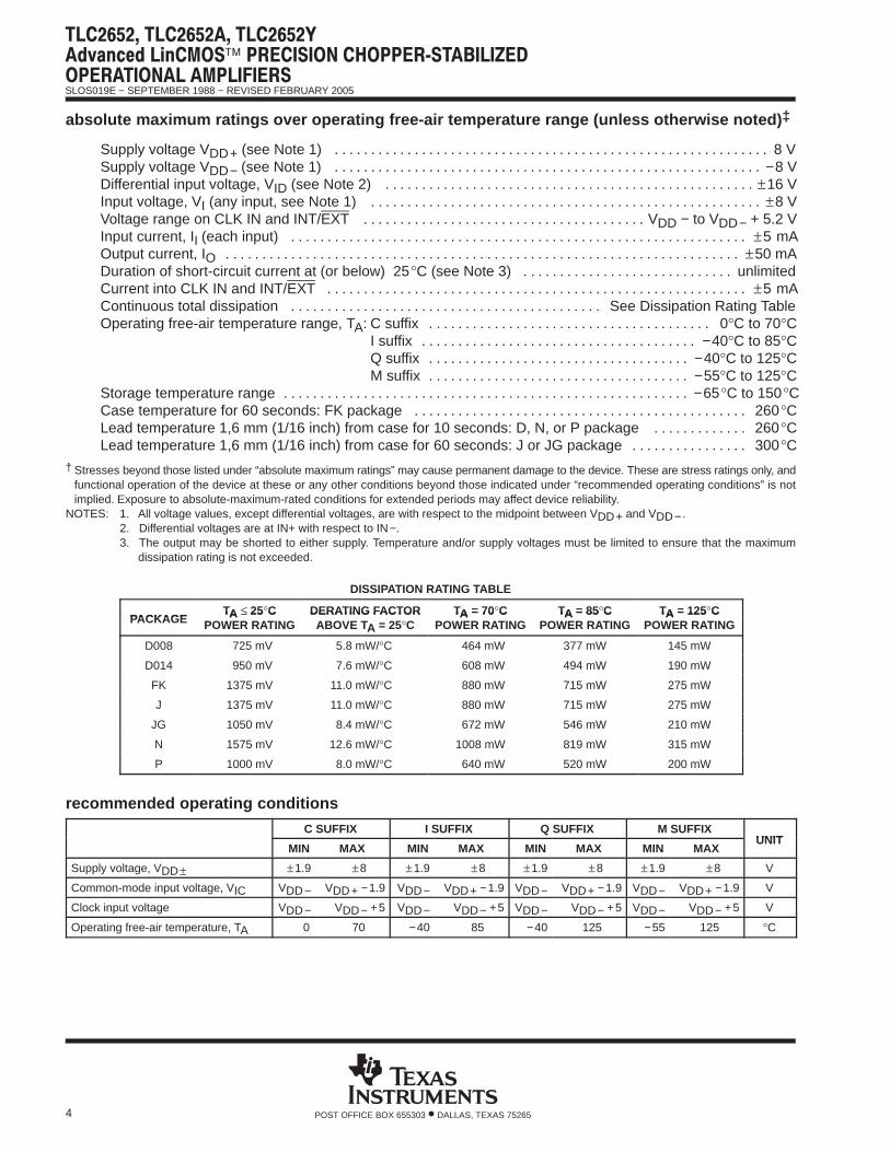
absolute maximum ratings over operating free-air temperature range (unless otherwise noted) ‡
Supply voltage VDD+ (see Note 1) 8 V. . . . . . . . . . . . . . . . . . . . . . . . . . . . . . . . . . . . . . . . . . . . . . . . . . . . . . . . . . . . Supply voltage VDD− (see Note 1) −8 V. . . . . . . . . . . . . . . . . . . . . . . . . . . . . . . . . . . . . . . . . . . . . . . . . . . . . . . . . . . Differential input voltage, VID (see Note 2) ±16 V. . . . . . . . . . . . . . . . . . . . . . . . . . . . . . . . . . . . . . . . . . . . . . . . . . . Input voltage, VI (any input, see Note 1) ±8 V. . . . . . . . . . . . . . . . . . . . . . . . . . . . . . . . . . . . . . . . . . . . . . . . . . . . . . Voltage range on CLK IN and INT/EXT VDD − to VDD− + 5.2 V. . . . . . . . . . . . . . . . . . . . . . . . . . . . . . . . . . . . . . . Input current, II (each input) ±5 mA. . . . . . . . . . . . . . . . . . . . . . . . . . . . . . . . . . . . . . . . . . . . . . . . . . . . . . . . . . . . . . . Output current, IO ±50 mA. . . . . . . . . . . . . . . . . . . . . . . . . . . . . . . . . . . . . . . . . . . . . . . . . . . . . . . . . . . . . . . . . . . . . . . Duration of short-circuit current at (or below) 25°C (see Note 3) unlimited. . . . . . . . . . . . . . . . . . . . . . . . . . . . . Current into CLK IN and INT/EXT ±5 mA. . . . . . . . . . . . . . . . . . . . . . . . . . . . . . . . . . . . . . . . . . . . . . . . . . . . . . . . . . Continuous total dissipation See Dissipation Rating Table. . . . . . . . . . . . . . . . . . . . . . . . . . . . . . . . . . . . . . . . . . . Operating free-air temperature range, TA: C suffix 0°C to 70°C. . . . . . . . . . . . . . . . . . . . . . . . . . . . . . . . . . . . . . .
I suffix −40°C to 85°C. . . . . . . . . . . . . . . . . . . . . . . . . . . . . . . . . . . . . . Q suffix −40°C to 125°C. . . . . . . . . . . . . . . . . . . . . . . . . . . . . . . . . . . . M suffix −55°C to 125°C. . . . . . . . . . . . . . . . . . . . . . . . . . . . . . . . . . . .
Storage temperature range −65°C to 150°C. . . . . . . . . . . . . . . . . . . . . . . . . . . . . . . . . . . . . . . . . . . . . . . . . . . . . . . . Case temperature for 60 seconds: FK package 260°C. . . . . . . . . . . . . . . . . . . . . . . . . . . . . . . . . . . . . . . . . . . . . . Lead temperature 1,6 mm (1/16 inch) from case for 10 seconds: D, N, or P package 260°C. . . . . . . . . . . . . Lead temperature 1,6 mm (1/16 inch) from case for 60 seconds: J or JG package 300°C. . . . . . . . . . . . . . . .
† Stresses beyond those listed under “absolute maximum ratings” may cause permanent damage to the device. These are stress ratings only, andfunctional operation of the device at these or any other conditions beyond those indicated under “recommended operating conditions” is notimplied. Exposure to absolute-maximum-rated conditions for extended periods may affect device reliability.
NOTES: 1. All voltage values, except differential voltages, are with respect to the midpoint between VDD+ and VDD−.2. Differential voltages are at IN+ with respect to IN−.3. The output may be shorted to either supply. Temperature and/or supply voltages must be limited to ensure that the maximum
dissipation rating is not exceeded.
DISSIPATION RATING TABLE
PACKAGETA ≤ 25°C DERATING FACTOR TA = 70°C TA = 85°C TA = 125°C
PACKAGETA ≤ 25 C
POWER RATINGDERATING FACTORABOVE TA = 25°C
TA = 70 CPOWER RATING
TA = 85 CPOWER RATING
TA = 125 CPOWER RATING
D008 725 mV 5.8 mW/°C 464 mW 377 mW 145 mW
D014 950 mV 7.6 mW/°C 608 mW 494 mW 190 mW
FK 1375 mV 11.0 mW/°C 880 mW 715 mW 275 mW
J 1375 mV 11.0 mW/°C 880 mW 715 mW 275 mW
JG 1050 mV 8.4 mW/°C 672 mW 546 mW 210 mW
N 1575 mV 12.6 mW/°C 1008 mW 819 mW 315 mW
P 1000 mV 8.0 mW/°C 640 mW 520 mW 200 mW
recommended operating conditions
C SUFFIX I SUFFIX Q SUFFIX M SUFFIXUNIT
MIN MAX MIN MAX MIN MAX MIN MAXUNIT
Supply voltage, VDD± ±1.9 ±8 ±1.9 ±8 ±1.9 ±8 ±1.9 ±8 V
Common-mode input voltage, VIC VDD− VDD+ −1.9 VDD− VDD+ −1.9 VDD− VDD+ −1.9 VDD− VDD+ −1.9 V
Clock input voltage VDD− VDD− +5 VDD− VDD− +5 VDD− VDD− +5 VDD− VDD− +5 V
Operating free-air temperature, TA 0 70 −40 85 −40 125 −55 125 °C
SLOS019E − SEPTEMBER 1988 − REVISED FEBRUARY 2005
5POST OFFICE BOX 655303 • DALLAS, TEXAS 75265
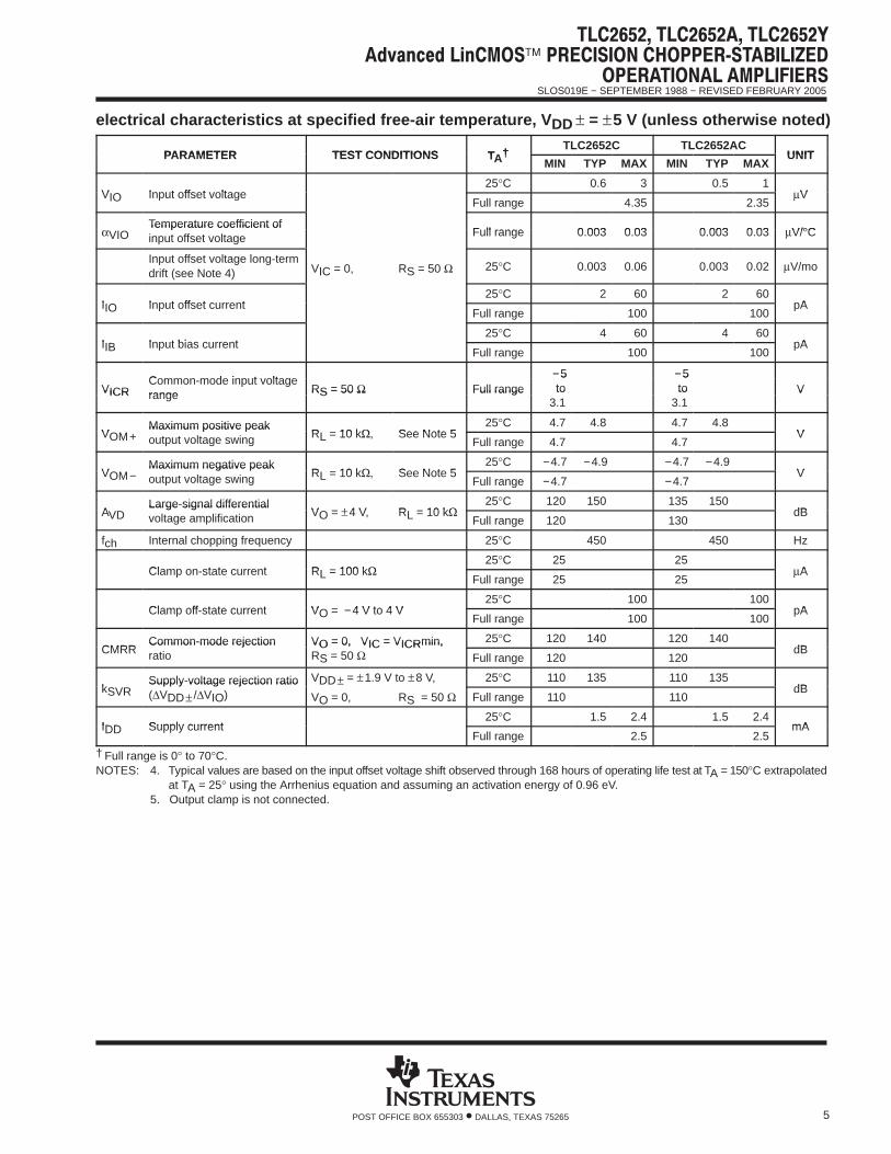
electrical characteristics at specified free-air temperature, V DD ± = ±5 V (unless otherwise noted)
PARAMETER TEST CONDITIONS TA†TLC2652C TLC2652AC
UNITPARAMETER TEST CONDITIONS TA†MIN TYP MAX MIN TYP MAX
UNIT
VIO Input offset voltage25°C 0.6 3 0.5 1
VVIO Input offset voltageFull range 4.35 2.35
µV
VIOTemperature coefficient of
Full range 0.003 0.03 0.003 0.03 V/°CαVIOTemperature coefficient ofinput offset voltage Full range 0.003 0.03 0.003 0.03 µV/°C
Input offset voltage long-termdrift (see Note 4) VIC = 0, RS = 50 Ω 25°C 0.003 0.06 0.003 0.02 µV/mo
IIO Input offset current25°C 2 60 2 60
pAIIO Input offset currentFull range 100 100
pA
IIB Input bias current25°C 4 60 4 60
pAIIB Input bias currentFull range 100 100
pA
Common-mode input voltage−5 −5
VICRCommon-mode input voltagerange RS = 50 Ω Full range
−5to
−5to VVICR range RS = 50 Ω Full range to
3.1to
3.1V
VOM+Maximum positive peak
RL = 10 kΩ See Note 525°C 4.7 4.8 4.7 4.8
VVOM+Maximum positive peakoutput voltage swing RL = 10 kΩ, See Note 5
Full range 4.7 4.7V
VOM−Maximum negative peak
RL = 10 kΩ See Note 525°C −4.7 −4.9 −4.7 −4.9
VVOM−Maximum negative peakoutput voltage swing RL = 10 kΩ, See Note 5
Full range −4.7 −4.7V
AVDLarge-signal differential
VO = ±4 V, RL = 10 kΩ25°C 120 150 135 150
dBAVDLarge-signal differentialvoltage amplification VO = ±4 V, RL = 10 kΩ
Full range 120 130dB
fch Internal chopping frequency 25°C 450 450 Hz
Clamp on-state current RL = 100 kΩ25°C 25 25
AClamp on-state current RL = 100 kΩFull range 25 25
µA
Clamp off-state current VO = −4 V to 4 V25°C 100 100
pAClamp off-state current VO = −4 V to 4 VFull range 100 100
pA
CMRRCommon-mode rejection VO = 0, VIC = VICRmin, 25°C 120 140 120 140
dBCMRRCommon-mode rejectionratio
VO = 0, VIC = VICRmin,RS = 50 Ω Full range 120 120
dB
kSVRSupply-voltage rejection ratio VDD± = ±1.9 V to ±8 V, 25°C 110 135 110 135
dBkSVRSupply-voltage rejection ratio(∆VDD± /∆VIO) VO = 0, RS = 50 Ω Full range 110 110
dB
IDD Supply current25°C 1.5 2.4 1.5 2.4
mAIDD Supply currentFull range 2.5 2.5
mA
† Full range is 0° to 70°C.NOTES: 4. Typical values are based on the input offset voltage shift observed through 168 hours of operating life test at TA = 150°C extrapolated
at TA = 25° using the Arrhenius equation and assuming an activation energy of 0.96 eV.5. Output clamp is not connected.
SLOS019E − SEPTEMBER 1988 − REVISED FEBRUARY 2005
6 POST OFFICE BOX 655303 • DALLAS, TEXAS 75265
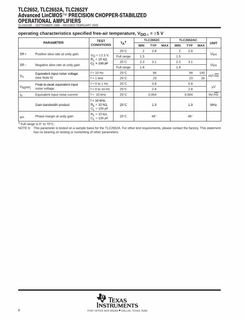
operating characteristics specified free-air temperature, V DD± = ±5 V
PARAMETERTEST
TA†TLC2652C TLC2652AC
UNITPARAMETERTEST
CONDITIONSTA†
MIN TYP MAX MIN TYP MAXUNIT
SR+ Positive slew rate at unity gain V = 2.3 V,25°C 2 2.8 2 2.8
V/ sSR+ Positive slew rate at unity gain VO = ±2.3 V,RL = 10 kΩ,
Full range 1.5 1.5V/µs
SR− Negative slew rate at unity gain
ORL = 10 kΩ,CL = 100 pF 25°C 2.3 3.1 2.3 3.1
V/ sSR− Negative slew rate at unity gain CL = 100 pFFull range 1.8 1.8
V/µs
VnEquivalent input noise voltage f = 10 Hz 25°C 94 94 140
nV/√HzVnEquivalent input noise voltage(see Note 6) f = 1 kHz 25°C 23 23 35
nV/√Hz
VN(PP)Peak-to-peak equivalent input f = 0 to 1 Hz 25°C 0.8 0.8
VVN(PP)Peak-to-peak equivalent inputnoise voltage f = 0 to 10 Hz 25°C 2.8 2.8
µV
In Equivalent input noise current f = 10 kHz 25°C 0.004 0.004 fA/√Hz
f = 10 kHz,Gain-bandwidth product
f = 10 kHz,RL = 10 kΩ, 25°C 1.9 1.9 MHzGain-bandwidth product RL = 10 kΩ,CL = 100 pF
25 C 1.9 1.9 MHz
φm Phase margin at unity gainRL = 10 kΩ,CL = 100 pF
25°C 48° 48°
† Full range is 0° to 70°C.NOTE 6: This parameter is tested on a sample basis for the TLC2652A. For other test requirements, please contact the factory. This statement
has no bearing on testing or nontesting of other parameters.

SLOS019E − SEPTEMBER 1988 − REVISED FEBRUARY 2005
7POST OFFICE BOX 655303 • DALLAS, TEXAS 75265
electrical characteristics at specified free-air temperature, V DD ± = ±5 V (unless otherwise noted)
PARAMETER TEST CONDITIONS TA†TLC2652I TLC2652AI
UNITPARAMETER TEST CONDITIONS TA†MIN TYP MAX MIN TYP MAX
UNIT
VIO Input offset voltage25°C 0.6 3 0.5 1
VVIO Input offset voltageFull range 4.95 2.95
µV
VIOTemperature coefficient of
Full range 0.003 0.03 0.003 0.03 V/°CαVIOTemperature coefficient ofinput offset voltage Full range 0.003 0.03 0.003 0.03 µV/°C
Input offset voltagelong-term drift (see Note 4) VIC = 0, RS = 50 Ω 25°C 0.003 0.06 0.003 0.02 µV/mo
IIO Input offset current25°C 2 60 2 60
pAIIO Input offset currentFull range 150 150
pA
IIB Input bias current25°C 4 60 4 60
pAIIB Input bias currentFull range 150 150
pA
Common-mode input−5 −5
VICRCommon-mode inputvoltage range RS = 50 Ω Full range
−5to
−5to VVICR voltage range RS = 50 Ω Full range to
3.1to
3.1V
VOM+Maximum positive peak
RL = 10 kΩ See Note 525°C 4.7 4.8 4.7 4.8
VVOM+Maximum positive peakoutput voltage swing RL = 10 kΩ, See Note 5
Full range 4.7 4.7V
VOM−Maximum negative peak
RL = 10 kΩ See Note 525°C −4.7 −4.9 −4.7 −4.9
VVOM−Maximum negative peakoutput voltage swing RL = 10 kΩ, See Note 5
Full range −4.7 −4.7V
AVDLarge-signal differential
VO = ±4 V, RL = 10 kΩ25°C 120 150 135 150
dBAVDLarge-signal differentialvoltage amplification VO = ±4 V, RL = 10 kΩ
Full range 120 125dB
Internal chopping frequency 25°C 450 450 Hz
Clamp on-state current RL = 100 kΩ25°C 25 25
AClamp on-state current RL = 100 kΩFull range 25 25
µA
Clamp off-state current VO = −4 V to 4 V25°C 100 100
pAClamp off-state current VO = −4 V to 4 VFull range 100 100
pA
CMRRCommon-mode rejection VO = 0, VIC = VICRmin, 25°C 120 140 120 140
dBCMRRCommon-mode rejectionratio
VO = 0, VIC = VICRmin,RS = 50 Ω Full range 120 120
dB
kSVRSupply-voltage rejection VDD± = ±1.9 V to ±8 V, 25°C 110 135 110 135
dBkSVRSupply-voltage rejectionratio (∆VDD± /∆VIO) VO = 0, RS = 50 Ω Full range 110 110
dB
IDD Supply current VO = 0, No load25°C 1.5 2.4 1.5 2.4
mAIDD Supply current VO = 0, No loadFull range 2.5 2.5
mA
† Full range is −40° to 85°C.NOTES: 4. Typical values are based on the input offset voltage shift observed through 168 hours of operating life test at TA = 150°C extrapolated
at TA = 25° using the Arrhenius equation and assuming an activation energy of 0.96 eV.5. Output clamp is not connected.

SLOS019E − SEPTEMBER 1988 − REVISED FEBRUARY 2005
8 POST OFFICE BOX 655303 • DALLAS, TEXAS 75265
operating characteristics at specified free-air temperature, V DD± = ±5 V
PARAMETERTEST
TA†TLC2652I TLC2652AI
UNITPARAMETERTEST
CONDITIONSTA†
MIN TYP MAX MIN TYP MAXUNIT
SR+ Positive slew rate at unity gain V = 2.3 V,25°C 2 2.8 2 2.8
V/ sSR+ Positive slew rate at unity gain VO = ±2.3 V,RL = 10 kΩ,
Full range 1.4 1.4V/µs
SR− Negative slew rate at unity gain
ORL = 10 kΩ,CL = 100 pF 25°C 2.3 3.1 2.3 3.1
V/ sSR− Negative slew rate at unity gain CL = 100 pFFull range 1.7 1.7
V/µs
VnEquivalent input noise voltage f = 10 Hz 25°C 94 94 140
nV/√HzVnEquivalent input noise voltage(see Note 6) f = 1 kHz 25°C 23 23 35
nV/√Hz
VN(PP)Peak-to-peak equivalent input f = 0 to 1 Hz 25°C 0.8 0.8
VVN(PP)Peak-to-peak equivalent inputnoise voltage f = 0 to 10 Hz 25°C 2.8 2.8
µV
In Equivalent input noise current f = 1 kHz 25°C 0.004 0.004 pA/√Hz
f = 10 kHz,Gain-bandwidth product
f = 10 kHz,RL = 10 kΩ, 25°C 1.9 1.9 MHzGain-bandwidth product RL = 10 kΩ,CL = 100 pF
25 C 1.9 1.9 MHz
φm Phase margin at unity gainRL = 10 kΩ,CL = 100 pF
25°C 48° 48°
† Full range is −40° to 85°C.NOTE 6: This parameter is tested on a sample basis for the TLC2652A. For other test requirements, please contact the factory. This statement
has no bearing on testing or nontesting of other parameters.
SLOS019E − SEPTEMBER 1988 − REVISED FEBRUARY 2005
9POST OFFICE BOX 655303 • DALLAS, TEXAS 75265
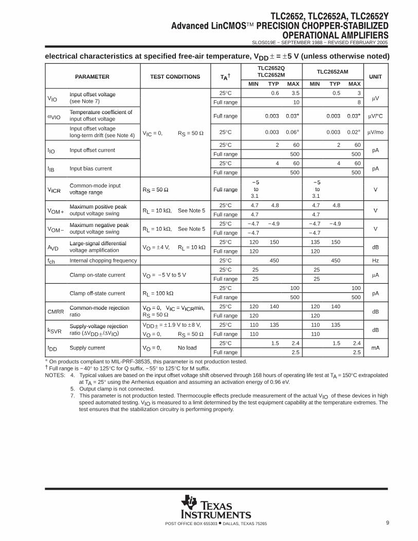
electrical characteristics at specified free-air temperature, V DD ± = ±5 V (unless otherwise noted)
PARAMETER TEST CONDITIONS TA†TLC2652QTLC2652M TLC2652AM
UNITPARAMETER TEST CONDITIONS TA†
MIN TYP MAX MIN TYP MAXUNIT
VIOInput offset voltage 25°C 0.6 3.5 0.5 3
VVIOInput offset voltage (see Note 7) Full range 10 8
µV
VIOTemperature coefficient of
Full range 0.003 0.03∗ 0.003 0.03∗ V/°CαVIOTemperature coefficient ofinput offset voltage Full range 0.003 0.03∗ 0.003 0.03∗ µV/°C
Input offset voltagelong-term drift (see Note 4) VIC = 0, RS = 50 Ω 25°C 0.003 0.06∗ 0.003 0.02∗ µV/mo
IIO Input offset current25°C 2 60 2 60
pAIIO Input offset currentFull range 500 500
pA
IIB Input bias current25°C 4 60 4 60
pAIIB Input bias currentFull range 500 500
pA
Common-mode input−5 −5
VICRCommon-mode inputvoltage range RS = 50 Ω Full range
−5to
−5to VVICR voltage range RS = 50 Ω Full range to
3.1to
3.1V
VOM+Maximum positive peak
RL = 10 kΩ See Note 525°C 4.7 4.8 4.7 4.8
VVOM+Maximum positive peakoutput voltage swing RL = 10 kΩ, See Note 5
Full range 4.7 4.7V
VOM−Maximum negative peak
RL = 10 kΩ See Note 525°C −4.7 −4.9 −4.7 −4.9
VVOM−Maximum negative peakoutput voltage swing RL = 10 kΩ, See Note 5
Full range −4.7 −4.7V
AVDLarge-signal differential
VO = ±4 V, RL = 10 kΩ25°C 120 150 135 150
dBAVDLarge-signal differentialvoltage amplification VO = ±4 V, RL = 10 kΩ
Full range 120 120dB
fch Internal chopping frequency 25°C 450 450 Hz
Clamp on-state current VO = −5 V to 5 V25°C 25 25
AClamp on-state current VO = −5 V to 5 VFull range 25 25
µA
Clamp off-state current RL = 100 kΩ25°C 100 100
pAClamp off-state current RL = 100 kΩFull range 500 500
pA
CMRRCommon-mode rejection VO = 0, VIC = VICRmin, 25°C 120 140 120 140
dBCMRRCommon-mode rejectionratio
VO = 0, VIC = VICRmin,RS = 50 Ω Full range 120 120
dB
kSVRSupply-voltage rejection VDD± = ±1.9 V to ±8 V, 25°C 110 135 110 135
dBkSVRSupply-voltage rejectionratio (∆VDD± /∆VIO) VO = 0, RS = 50 Ω Full range 110 110
dB
IDD Supply current VO = 0, No load25°C 1.5 2.4 1.5 2.4
mAIDD Supply current VO = 0, No loadFull range 2.5 2.5
mA
∗ On products compliant to MIL-PRF-38535, this parameter is not production tested.† Full range is −40° to 125°C for Q suffix, −55° to 125°C for M suffix.NOTES: 4. Typical values are based on the input offset voltage shift observed through 168 hours of operating life test at TA = 150°C extrapolated
at TA = 25° using the Arrhenius equation and assuming an activation energy of 0.96 eV.5. Output clamp is not connected.7. This parameter is not production tested. Thermocouple effects preclude measurement of the actual VIO of these devices in high
speed automated testing. VIO is measured to a limit determined by the test equipment capability at the temperature extremes. Thetest ensures that the stabilization circuitry is performing properly.
SLOS019E − SEPTEMBER 1988 − REVISED FEBRUARY 2005
10 POST OFFICE BOX 655303 • DALLAS, TEXAS 75265
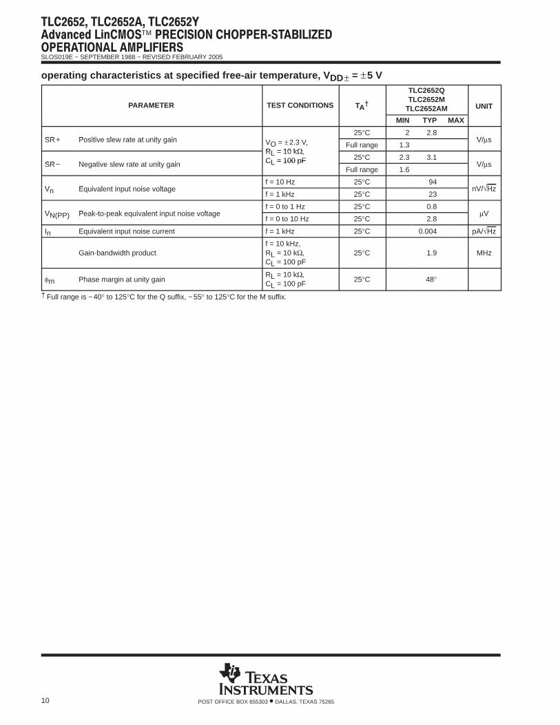
operating characteristics at specified free-air temperature, V DD± = ±5 V
PARAMETER TEST CONDITIONS TA†
TLC2652QTLC2652M
TLC2652AM UNITA
MIN TYP MAX
SR+ Positive slew rate at unity gain V = 2.3 V, 25°C 2 2.8
V/ sSR+ Positive slew rate at unity gain VO = ±2.3 V, RL = 10 kΩ,
Full range 1.3V/µs
SR− Negative slew rate at unity gain
ORL = 10 kΩ,CL = 100 pF 25°C 2.3 3.1
V/ sSR− Negative slew rate at unity gain CL = 100 pFFull range 1.6
V/µs
Vn Equivalent input noise voltagef = 10 Hz 25°C 94
nV/√HzVn Equivalent input noise voltagef = 1 kHz 25°C 23
nV/√Hz
VN(PP) Peak-to-peak equivalent input noise voltagef = 0 to 1 Hz 25°C 0.8
VVN(PP) Peak-to-peak equivalent input noise voltagef = 0 to 10 Hz 25°C 2.8
µV
In Equivalent input noise current f = 1 kHz 25°C 0.004 pA/√Hz
Gain-bandwidth productf = 10 kHz,RL = 10 kΩ,CL = 100 pF
25°C 1.9 MHz
φm Phase margin at unity gainRL = 10 kΩ,CL = 100 pF
25°C 48°
† Full range is −40° to 125°C for the Q suffix, −55° to 125°C for the M suffix.
SLOS019E − SEPTEMBER 1988 − REVISED FEBRUARY 2005
11POST OFFICE BOX 655303 • DALLAS, TEXAS 75265
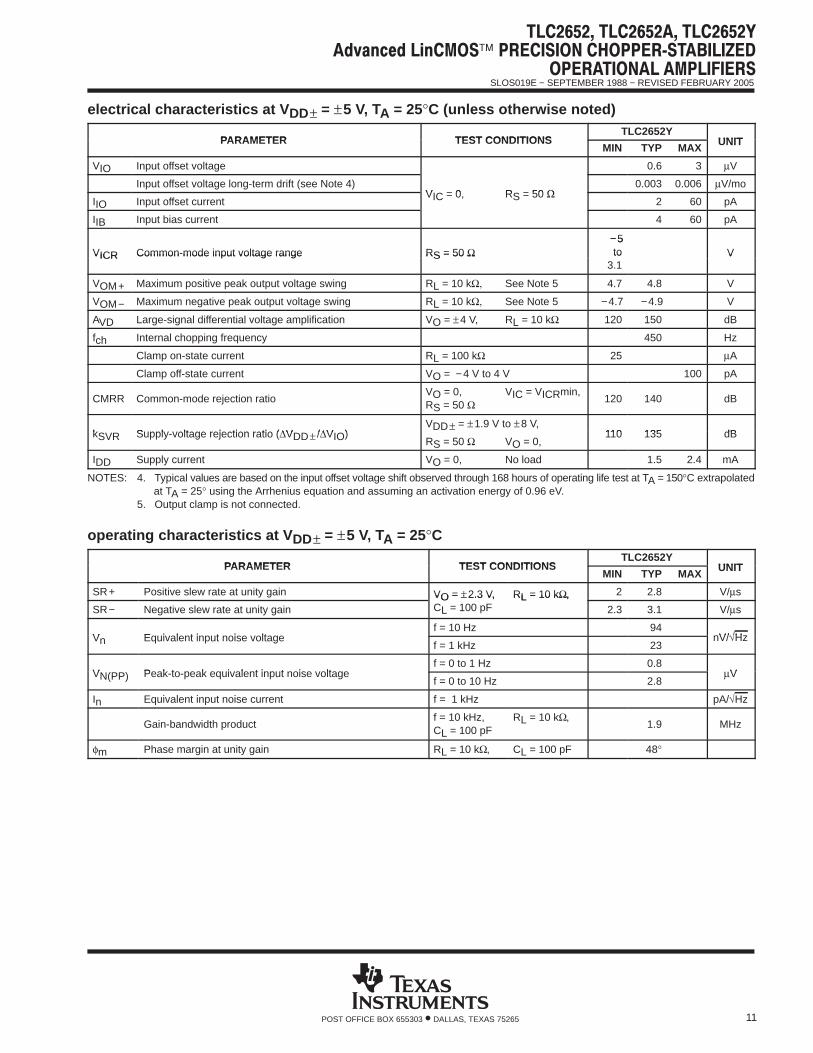
electrical characteristics at V DD± = ±5 V, TA = 25°C (unless otherwise noted)
PARAMETER TEST CONDITIONSTLC2652Y
UNITPARAMETER TEST CONDITIONSMIN TYP MAX
UNIT
VIO Input offset voltage 0.6 3 µV
Input offset voltage long-term drift (see Note 4)VIC = 0, RS = 50 Ω
0.003 0.006 µV/mo
IIO Input offset currentVIC = 0, RS = 50 Ω
2 60 pA
IIB Input bias current 4 60 pA
−5VICR Common-mode input voltage range RS = 50 Ω
−5to VVICR Common-mode input voltage range RS = 50 Ω to
3.1V
VOM+ Maximum positive peak output voltage swing RL = 10 kΩ, See Note 5 4.7 4.8 V
VOM− Maximum negative peak output voltage swing RL = 10 kΩ, See Note 5 −4.7 −4.9 V
AVD Large-signal differential voltage amplification VO = ±4 V, RL = 10 kΩ 120 150 dB
fch Internal chopping frequency 450 Hz
Clamp on-state current RL = 100 kΩ 25 µA
Clamp off-state current VO = −4 V to 4 V 100 pA
CMRR Common-mode rejection ratioVO = 0,RS = 50 Ω
VIC = VICRmin,120 140 dB
kSVR Supply-voltage rejection ratio (∆VDD /∆VIO)VDD± = ±1.9 V to ±8 V,
110 135 dBkSVR Supply-voltage rejection ratio (∆VDD± /∆VIO)RS = 50 Ω VO = 0,
110 135 dB
IDD Supply current VO = 0, No load 1.5 2.4 mA
NOTES: 4. Typical values are based on the input offset voltage shift observed through 168 hours of operating life test at TA = 150°C extrapolatedat TA = 25° using the Arrhenius equation and assuming an activation energy of 0.96 eV.
5. Output clamp is not connected.
operating characteristics at V DD± = ±5 V, TA = 25°C
PARAMETER TEST CONDITIONSTLC2652Y
UNITPARAMETER TEST CONDITIONSMIN TYP MAX
UNIT
SR+ Positive slew rate at unity gain VO = ±2.3 V, RL = 10 kΩ, 2 2.8 V/µs
SR− Negative slew rate at unity gain
VO = ±2.3 V,CL = 100 pF
RL = 10 kΩ,
2.3 3.1 V/µs
Vn Equivalent input noise voltagef = 10 Hz 94
nV/√HzVn Equivalent input noise voltagef = 1 kHz 23
nV/√Hz
VN(PP) Peak-to-peak equivalent input noise voltagef = 0 to 1 Hz 0.8
VVN(PP) Peak-to-peak equivalent input noise voltagef = 0 to 10 Hz 2.8
µV
In Equivalent input noise current f = 1 kHz pA/√Hz
Gain-bandwidth productf = 10 kHz,CL = 100 pF
RL = 10 kΩ,1.9 MHz
φm Phase margin at unity gain RL = 10 kΩ, CL = 100 pF 48°
SLOS019E − SEPTEMBER 1988 − REVISED FEBRUARY 2005
12 POST OFFICE BOX 655303 • DALLAS, TEXAS 75265
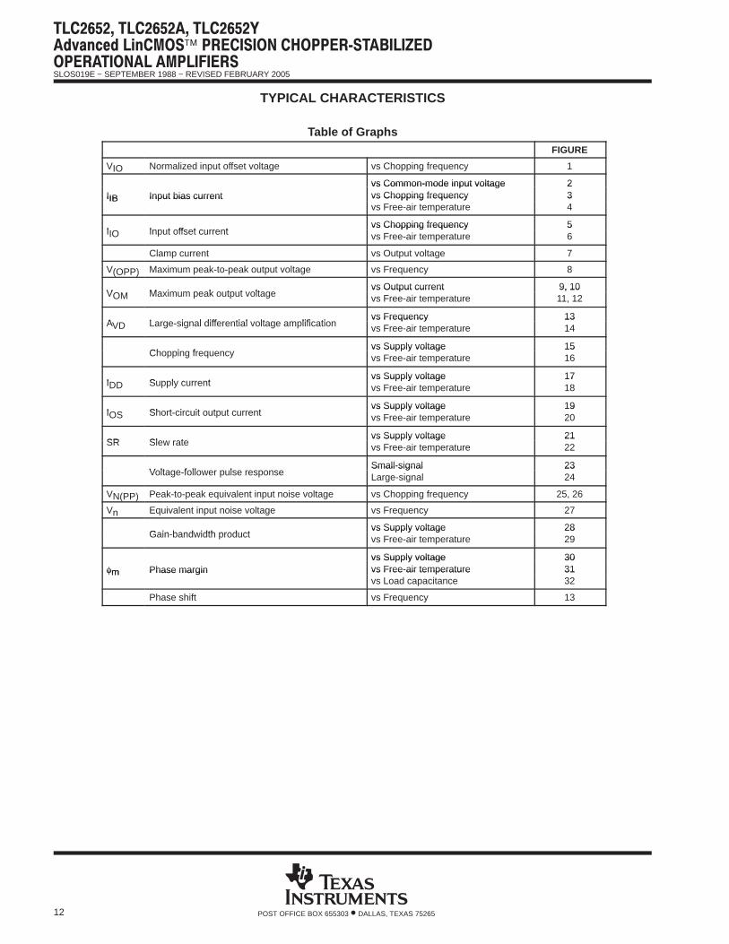
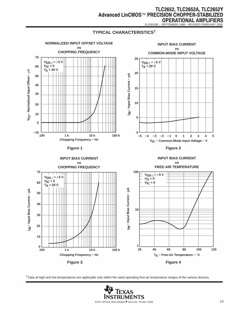
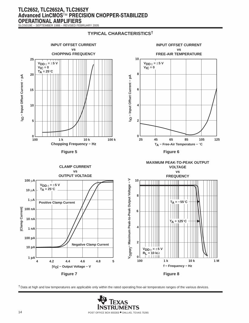
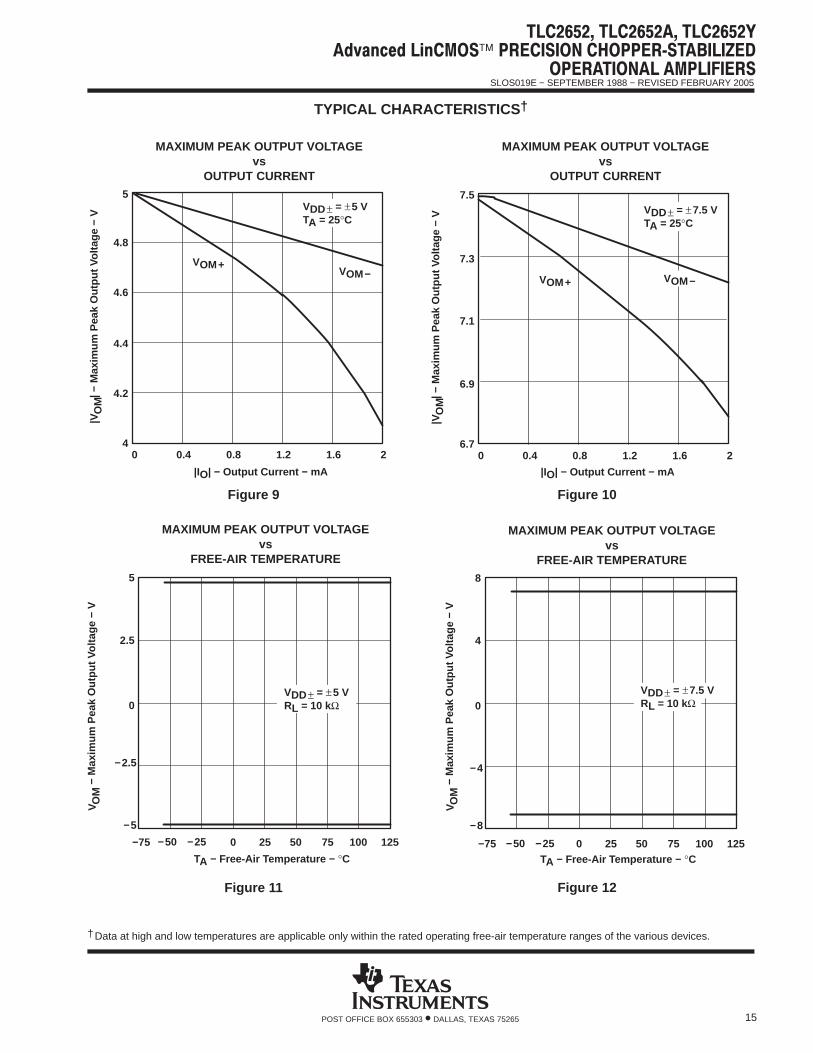
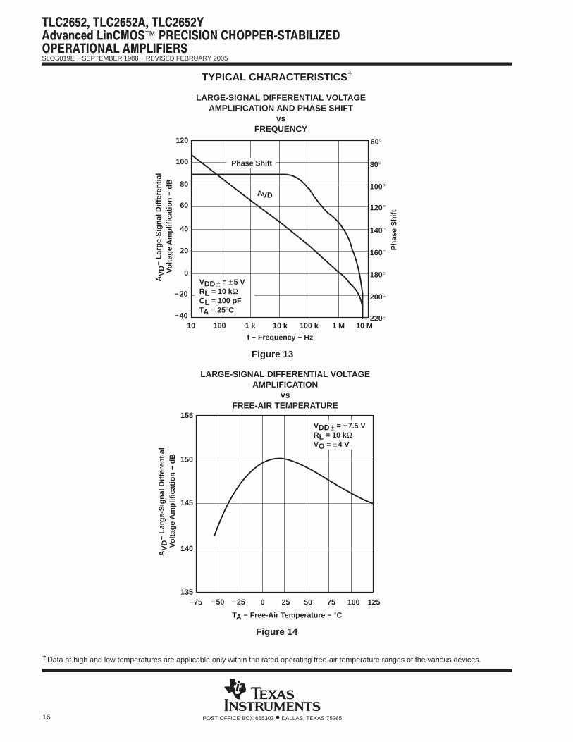
TYPICAL CHARACTERISTICS
Table of GraphsFIGURE
VIO Normalized input offset voltage vs Chopping frequency 1
vs Common-mode input voltage 2IIB Input bias current
vs Common-mode input voltagevs Chopping frequency
23IIB Input bias current vs Chopping frequency
vs Free-air temperature34
IIO Input offset currentvs Chopping frequency 5
IIO Input offset currentvs Chopping frequencyvs Free-air temperature
56
Clamp current vs Output voltage 7
V(OPP) Maximum peak-to-peak output voltage vs Frequency 8
VOM Maximum peak output voltagevs Output current 9, 10
VOM Maximum peak output voltagevs Output currentvs Free-air temperature
9, 1011, 12
AVD Large-signal differential voltage amplificationvs Frequency 13
AVD Large-signal differential voltage amplificationvs Frequencyvs Free-air temperature
1314
Chopping frequencyvs Supply voltage 15
Chopping frequencyvs Supply voltagevs Free-air temperature
1516
IDD Supply currentvs Supply voltage 17
IDD Supply currentvs Supply voltagevs Free-air temperature
1718
IOS Short-circuit output currentvs Supply voltage 19
IOS Short-circuit output currentvs Supply voltagevs Free-air temperature
1920
SR Slew ratevs Supply voltage 21
SR Slew ratevs Supply voltagevs Free-air temperature
2122
Voltage-follower pulse responseSmall-signal 23
Voltage-follower pulse responseSmall-signalLarge-signal
2324
VN(PP) Peak-to-peak equivalent input noise voltage vs Chopping frequency 25, 26
Vn Equivalent input noise voltage vs Frequency 27
Gain-bandwidth productvs Supply voltage 28
Gain-bandwidth productvs Supply voltagevs Free-air temperature
2829
vs Supply voltage 30φm Phase margin
vs Supply voltagevs Free-air temperature
3031φm Phase margin vs Free-air temperature
vs Load capacitance3132
Phase shift vs Frequency 13
SLOS019E − SEPTEMBER 1988 − REVISED FEBRUARY 2005
13POST OFFICE BOX 655303 • DALLAS, TEXAS 75265
TYPICAL CHARACTERISTICS †
NORMALIZED INPUT OFFSET VOLTAGEvs
CHOPPING FREQUENCY
−10
0
10
20
30
40
50
60
70
100 1 k 10 k 100 kChopping Frequency − Hz
VDD± = ±5 VVIC = 0TA = 25°C
VIO
− N
orm
aliz
ed In
put O
ffset
− u
VV
IOVµ
Figure 1
−5
VIC − Common-Mode Input Voltage − V
IIB −
Inpu
t Bia
s C
urre
nt −
pA
10
5
00 1
15
20
INPUT BIAS CURRENTvs
COMMON-MODE INPUT VOLTAGE
25
2 3 4 5
I IB
VDD± = ±5 VTA = 25°C
−4 −3 −2 −1
Figure 2
Figure 3
Chopping Frequency − Hz
30
10
0
60
20
IIB −
Inpu
t Bia
s C
urre
nt −
pA 50
40
70
INPUT BIAS CURRENTvs
CHOPPING FREQUENCY
100 1 k 10 k 100 k
IBI
VDD± = ±5 VVIC = 0TA = 25°C
TA − Free-Air Temperature − °C
1
100
25 45 65 105 125
INPUT BIAS CURRENTvs
FREE-AIR TEMPERATURE
85
10
VDD± = ±5 VVO = 0VIC = 0
IIB −
Inpu
t Bia
s C
urre
nt −
pA
IBI
Figure 4
†Data at high and low temperatures are applicable only within the rated operating free-air temperature ranges of the various devices.
SLOS019E − SEPTEMBER 1988 − REVISED FEBRUARY 2005
14 POST OFFICE BOX 655303 • DALLAS, TEXAS 75265
TYPICAL CHARACTERISTICS †
INPUT OFFSET CURRENTvs
CHOPPING FREQUENCY
Chopping Frequency − Hz
20
10
5
0
25
15
100 1 k 10 k 100 k
IIO −
Inpu
t Offs
et C
urre
nt −
pA
I IO
VDD± = ±5 VVIC = 0TA = 25°C
Figure 5 Figure 6
IIO −
Inpu
t Offs
et C
urre
nt −
pA
I IO
TA − Free-Air Temperature − °C
6
4
2
025 45 65 85
8
INPUT OFFSET CURRENTvs
FREE-AIR TEMPERATURE10
105 125
VDD± = ±5 VVIC = 0
|VO| − Output Voltage − V
1 nA
100 pA
10 pA
1 pA4 4.2 4.4 4.6
CLAMP CURRENTvs
OUTPUT VOLTAGE
4.8 5
100 nA
10 nA
VDD± = ±5 VTA = 25°C
Negative Clamp Current
100 µA
10 µA
1 µAPositive Clamp Current
|Cla
mp
Cur
rent
|
Figure 7
8
4
2
0
10
6
100 1 k 10 k 1 M
VO
(PP
) −
Max
imum
Pea
k-to
-Pea
k O
utpu
t Vol
tage
− V
f − Frequency − Hz
MAXIMUM PEAK-TO-PEAK OUTPUTVOLTAGE
vsFREQUENCY
VO
(PP
) VDD± = ±5 VRL = 10 kΩ
TA = 125°C
TA = −55°C
Figure 8
†Data at high and low temperatures are applicable only within the rated operating free-air temperature ranges of the various devices.
SLOS019E − SEPTEMBER 1988 − REVISED FEBRUARY 2005
15POST OFFICE BOX 655303 • DALLAS, TEXAS 75265
TYPICAL CHARACTERISTICS †
Figure 9
|IO| − Output Current − mA
4.6
4.4
4.2
40 0.4 0.8 1.2
4.8
MAXIMUM PEAK OUTPUT VOLTAGEvs
OUTPUT CURRENT5
1.6 2
VDD± = ±5 VTA = 25°C
VOM+VOM−
|VO
M| −
Max
imum
Pea
k O
utpu
t Vol
tage
− V
|V O
M
Figure 10
|IO| − Output Current − mA
7.1
6.9
6.70 0.4 0.8 1.2
7.3
MAXIMUM PEAK OUTPUT VOLTAGEvs
OUTPUT CURRENT
7.5
1.6 2
VDD± = ±7.5 VTA = 25°C
VOM+ VOM−
|VO
M| −
Max
imum
Pea
k O
utpu
t Vol
tage
− V
|V O
M
Figure 11
TA − Free-Air Temperature − °C
0
−75 0 25 50
2.5
MAXIMUM PEAK OUTPUT VOLTAGEvs
FREE-AIR TEMPERATURE
5
75 100 125
VDD± = ±5 VRL = 10 kΩ
−2.5
VO
M −
Max
imum
Pea
k O
utpu
t Vol
tage
− V
V OM
−5
−50 −25
Figure 12
VO
M −
Max
imum
Pea
k O
utpu
t Vol
tage
− V
0
4
MAXIMUM PEAK OUTPUT VOLTAGEvs
FREE-AIR TEMPERATURE8
TA − Free-Air Temperature − °C−75 0 25 50 75 100 125
VDD± = ±7.5 VRL = 10 kΩ
V OM
−50 −25
−8
−4
†Data at high and low temperatures are applicable only within the rated operating free-air temperature ranges of the various devices.
SLOS019E − SEPTEMBER 1988 − REVISED FEBRUARY 2005
16 POST OFFICE BOX 655303 • DALLAS, TEXAS 75265
TYPICAL CHARACTERISTICS †
20
0
40
60
80
10 100 1 k 10 k 100 k
f − Frequency − Hz
LARGE-SIGNAL DIFFERENTIAL VOLTAGEAMPLIFICATION AND PHASE SHIFT
vsFREQUENCY
1 M 10 M
100
120
220°
200°
180°
160°
140°
120°
100°
80°
60°
VDD± = ±5 VRL = 10 kΩCL = 100 pFTA = 25°C
AVD
−20
−40
Phase ShiftA
VD
− L
arge
-Sig
nal D
iffer
entia
l
ÁÁÁÁÁÁ
AV
D Vol
tage
Am
plifi
catio
n −
dB
Figure 13
Pha
se S
hift
Figure 14
−50 −25
145
140
135−75 0 25 50
150
LARGE-SIGNAL DIFFERENTIAL VOLTAGEAMPLIFICATION
vsFREE-AIR TEMPERATURE
155
75 100 125
TA − Free-Air Temperature − °C
VDD± = ±7.5 VRL = 10 kΩVO = ±4 V
AV
D −
Lar
ge-S
igna
l Diff
eren
tial
ÁÁÁÁÁÁ
AV
D Vol
tage
Am
plifi
catio
n −
dB
†Data at high and low temperatures are applicable only within the rated operating free-air temperature ranges of the various devices.
SLOS019E − SEPTEMBER 1988 − REVISED FEBRUARY 2005
17POST OFFICE BOX 655303 • DALLAS, TEXAS 75265
TYPICAL CHARACTERISTICS †
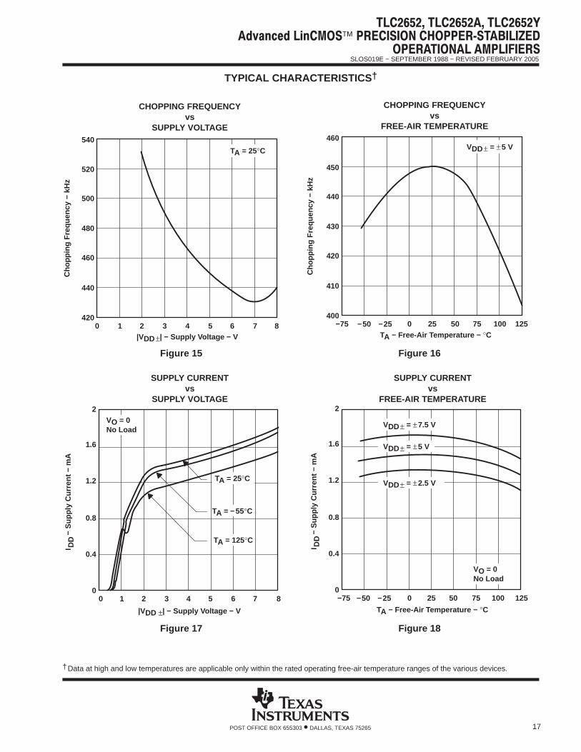
Figure 15
|VDD±| − Supply Voltage − V
480
460
440
4200 1 2 3 4 5
500
520
CHOPPING FREQUENCYvs
SUPPLY VOLTAGE540
6 7 8
TA = 25°C
Cho
ppin
g F
requ
ency
− k
Hz
Figure 16
−50 −25TA − Free-Air Temperature − °C
430
420
410
400−75 0 25 50
440
450
CHOPPING FREQUENCYvs
FREE-AIR TEMPERATURE460
75 100 125
VDD± = ±5 V
Cho
ppin
g F
requ
ency
− k
Hz
Figure 17
|VDD ±| − Supply Voltage − V
IDD
− S
uppl
y C
urre
nt −
mA
I DD
1.2
0.8
0.4
00 2 3 5
1.6
SUPPLY CURRENTvs
SUPPLY VOLTAGE2
7 81 4 6
TA = 25°C
TA = −55°C
TA = 125°C
VO = 0No Load
−50 −25
TA − Free-Air Temperature − °C
1.2
0.8
0.4
0−75 0 50
1.6
SUPPLY CURRENTvs
FREE-AIR TEMPERATURE2
100 12525 75
VDD± = ±5 V
VDD± = ±7.5 V
VDD± = ±2.5 V
VO = 0No Load
IDD
− S
uppl
y C
urre
nt −
mA
I DD
Figure 18
†Data at high and low temperatures are applicable only within the rated operating free-air temperature ranges of the various devices.
SLOS019E − SEPTEMBER 1988 − REVISED FEBRUARY 2005
18 POST OFFICE BOX 655303 • DALLAS, TEXAS 75265
TYPICAL CHARACTERISTICS †
Figure 19
−4
0
−120 1 2 3 4 5
IOS
− S
hort
-Circ
uit O
utpu
t Cur
rent
− m
A
4
8
SHORT-CIRCUIT OUTPUT CURRENTvs
SUPPLY VOLTAGE12
6 7 8|VDD ±| − Supply Voltage − V
I OS
VO = 0TA = 25°C
−8
VID = −100 mV
VID = 100 mV
Figure 20
−50 −25
0
−10
−15−75 0 25 50
5
10
SHORT-CIRCUIT OUTPUT CURRENTvs
FREE-AIR TEMPERATURE15
75 100 125TA − Free-Air Temperature − °C
VID = 100 mV
VID = −100 mV
VDD± = ±5 VVO = 0
IOS
− S
hort
-Circ
uit O
utpu
t Cur
rent
− m
AI O
S
−5
Figure 21
2
1
00 1 2 3 4 5
3
4
6 7 8|VDD±| − Supply Voltage − V
SLEW RATEvs
SUPPLY VOLTAGE
RL = 10 kΩCL = 100 pFTA = 25°C
SR−
SR+
SR
− S
lew
Rat
e −
V?u
ssµV
/
Figure 22
−50 −25
2
1
0−75 0 25 50
SR
− S
lew
Rat
e −
V?u
s
3
SLEW RATEvs
FREE-AIR TEMPERATURE4
75 100 125TA − Free-Air Temperature − °C
sµV
/
VDD± = ±5 VRL = 10 kΩ CL = 100 pF
SR+
SR−
†Data at high and low temperatures are applicable only within the rated operating free-air temperature ranges of the various devices.
SLOS019E − SEPTEMBER 1988 − REVISED FEBRUARY 2005
19POST OFFICE BOX 655303 • DALLAS, TEXAS 75265
TYPICAL CHARACTERISTICS
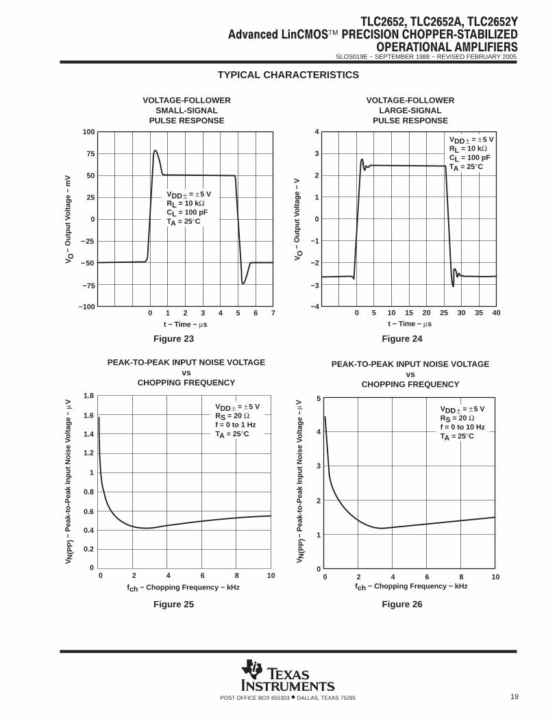
Figure 23
−25
t − Time − µs
VO
− O
utpu
t Vol
tage
− m
V
0
−75
−1000 1 2 3
25
75
VOLTAGE-FOLLOWERSMALL-SIGNAL
PULSE RESPONSE100
4 5 6 7
50
VO
VDD± = ±5 VRL = 10 kΩ CL = 100 pFTA = 25°C
−50
Figure 24
t − Time − µs
VO
− O
utpu
t Vol
tage
− V
VO
0
−1
−3
−40 5 10 15 20
1
3
VOLTAGE-FOLLOWERLARGE-SIGNAL
PULSE RESPONSE4
25 30 35 40
−2
2
VDD± = ±5 VRL = 10 kΩ CL = 100 pFTA = 25°C
Figure 25
fch − Chopping Frequency − kHz
PEAK-TO-PEAK INPUT NOISE VOLTAGEvs
CHOPPING FREQUENCY
0
0.2
0.4
0.6
0.8
1
1.2
1.4
1.6
1.8
0 2 4 6 8 10
VN
(PP
) −
Pea
k-to
-Pea
k In
put N
oise
Vol
tage
−uV
N(P
P)
V
VDD± = ±5 VRS = 20 Ω f = 0 to 1 HzTA = 25°C
µV
Figure 26
fch − Chopping Frequency − kHz
3
2
1
00 2 4 6
VN
(PP
) −
Pea
k-to
-Pea
k In
put N
oise
Vol
tage
− u
V
4
PEAK-TO-PEAK INPUT NOISE VOLTAGEvs
CHOPPING FREQUENCY
5
8 10
N(P
P)
V
VDD± = ±5 VRS = 20 Ω f = 0 to 10 HzTA = 25°C
µV
SLOS019E − SEPTEMBER 1988 − REVISED FEBRUARY 2005
20 POST OFFICE BOX 655303 • DALLAS, TEXAS 75265
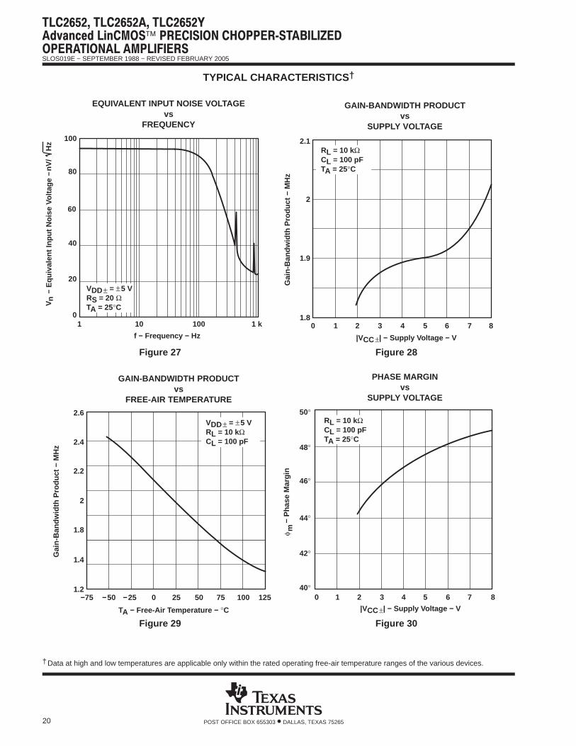
TYPICAL CHARACTERISTICS †
Vn
− E
quiv
alen
t Inp
ut N
oise
Vol
tage
− n
V/H
z
80
40
20
0
100
60
1 10 100 1 k
f − Frequency − Hz
EQUIVALENT INPUT NOISE VOLTAGEvs
FREQUENCY
Vn
VDD± = ±5 VRS = 20 Ω TA = 25°C
nV/
Hz
Figure 27 Figure 28
|VCC±| − Supply Voltage − V
1.9
1.80 1 2 3 4 5
Gai
n-B
andw
idth
Pro
duct
− M
Hz
2
GAIN-BANDWIDTH PRODUCTvs
SUPPLY VOLTAGE
2.1
6 7 8
RL = 10 kΩCL = 100 pFTA = 25°C
Figure 29
−50
TA − Free-Air Temperature − °C
2
1.8
1.4
1.2−75 0 25 50
Gai
n-B
andw
idth
Pro
duct
− M
Hz
2.2
2.4
GAIN-BANDWIDTH PRODUCTvs
FREE-AIR TEMPERATURE
2.6
75 100 125
VDD± = ±5 VRL = 10 kΩ CL = 100 pF
−25
Figure 30
|VCC±| − Supply Voltage − V
om −
Pha
se M
argi
n
0 2 3 5
PHASE MARGINvs
SUPPLY VOLTAGE
7 81 4 6
RL = 10 kΩCL = 100 pFTA = 25°C
φ m
50°
48°
46°
44°
42°
40°
†Data at high and low temperatures are applicable only within the rated operating free-air temperature ranges of the various devices.
SLOS019E − SEPTEMBER 1988 − REVISED FEBRUARY 2005
21POST OFFICE BOX 655303 • DALLAS, TEXAS 75265
TYPICAL CHARACTERISTICS †
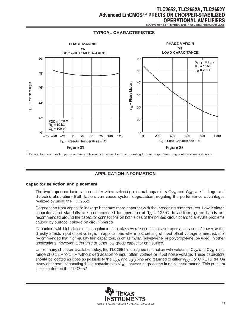
Figure 31
−50 −25
50°
48°
46°
44°
42°
40°
TA − Free-Air Temperature − °C−75 0 50
PHASE MARGINvs
FREE-AIR TEMPERATURE
100 12525 75
VDD± = ±5 VRL = 10 kΩCL = 100 pF
om −
Pha
se M
argi
n φ m
Figure 32
0 200 400 600
PHASE MARGINvs
LOAD CAPACITANCE
800 1000
VDD± = ±5 VRL = 10 kΩTA = 25°C
CL − Load Capacitance − pF
om −
Pha
se M
argi
n φ m
60°
50°
40°
30°
20°
10°
0°
†Data at high and low temperatures are applicable only within the rated operating free-air temperature ranges of the various devices.
APPLICATION INFORMATION
capacitor selection and placement
The two important factors to consider when selecting external capacitors CXA and CXB are leakage anddielectric absorption. Both factors can cause system degradation, negating the performance advantagesrealized by using the TLC2652.
Degradation from capacitor leakage becomes more apparent with the increasing temperatures. Low-leakagecapacitors and standoffs are recommended for operation at TA = 125°C. In addition, guard bands arerecommended around the capacitor connections on both sides of the printed circuit board to alleviate problemscaused by surface leakage on circuit boards.
Capacitors with high dielectric absorption tend to take several seconds to settle upon application of power, whichdirectly affects input offset voltage. In applications where fast settling of input offset voltage is needed, it isrecommended that high-quality film capacitors, such as mylar, polystyrene, or polypropylene, be used. In otherapplications, however, a ceramic or other low-grade capacitor can suffice.
Unlike many choppers available today, the TLC2652 is designed to function with values of CXA and CXB in therange of 0.1 µF to 1 µF without degradation to input offset voltage or input noise voltage. These capacitorsshould be located as close as possible to the CXA and CXB pins and returned to either VDD− or C RETURN. Onmany choppers, connecting these capacitors to VDD− causes degradation in noise performance. This problemis eliminated on the TLC2652.
SLOS019E − SEPTEMBER 1988 − REVISED FEBRUARY 2005
22 POST OFFICE BOX 655303 • DALLAS, TEXAS 75265
APPLICATION INFORMATION
internal/external clock
The TLC2652 has an internal clock that sets the chopping frequency to a nominal value of 450 Hz. On 8-pinpackages, the chopping frequency can only be controlled by the internal clock; however, on all 14-pin packagesand the 20-pin FK package, the device chopping frequency can be set by the internal clock or controlledexternally by use of the INT/EXT and CLK IN pins. To use the internal 450-Hz clock, no connection is necessary.If external clocking is desired, connect INT/EXT to VDD− and the external clock to CLK IN. The external clocktrip point is 2.5 V above the negative rail; however, CLK IN can be driven from the negative rail to 5 V abovethe negative rail. If this level is exceeded, damage could occur to the device unless the current into CLK IN islimited to ±5 mA. When operating in the single-supply configuration, this feature allows the TLC2652 to be drivendirectly by 5-V TTL and CMOS logic. A divide-by-two frequency divider interfaces with CLK IN andsets the clock chopping frequency. The duty cycleof the external clock is not critical but should bekept between 30% and 60%.
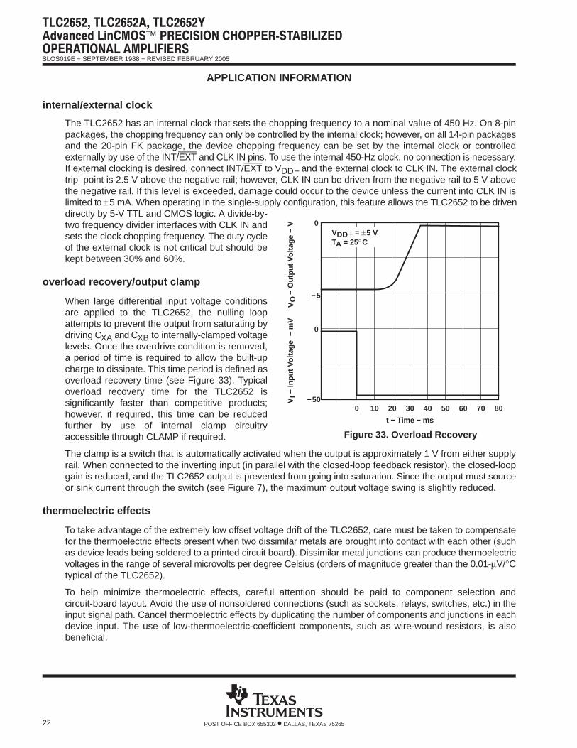
overload recovery/output clamp
When large differential input voltage conditionsare applied to the TLC2652, the nulling loopattempts to prevent the output from saturating bydriving CXA and CXB to internally-clamped voltagelevels. Once the overdrive condition is removed,a period of time is required to allow the built-upcharge to dissipate. This time period is defined asoverload recovery time (see Figure 33). Typicaloverload recovery time for the TLC2652 issignificantly faster than competitive products;however, if required, this time can be reducedfurther by use of internal clamp circuitryaccessible through CLAMP if required.
The clamp is a switch that is automatically activated when the output is approximately 1 V from either supplyrail. When connected to the inverting input (in parallel with the closed-loop feedback resistor), the closed-loopgain is reduced, and the TLC2652 output is prevented from going into saturation. Since the output must sourceor sink current through the switch (see Figure 7), the maximum output voltage swing is slightly reduced.
thermoelectric effects
To take advantage of the extremely low offset voltage drift of the TLC2652, care must be taken to compensatefor the thermoelectric effects present when two dissimilar metals are brought into contact with each other (suchas device leads being soldered to a printed circuit board). Dissimilar metal junctions can produce thermoelectricvoltages in the range of several microvolts per degree Celsius (orders of magnitude greater than the 0.01-µV/°Ctypical of the TLC2652).
To help minimize thermoelectric effects, careful attention should be paid to component selection andcircuit-board layout. Avoid the use of nonsoldered connections (such as sockets, relays, switches, etc.) in theinput signal path. Cancel thermoelectric effects by duplicating the number of components and junctions in eachdevice input. The use of low-thermoelectric-coefficient components, such as wire-wound resistors, is alsobeneficial.
0
0 10 20 30 40
VI −
Inpu
t Vol
tage
− m
V
VO
− O
utpu
t Vol
tage
− V
t − Time − ms
0
50 60 70 80
VI
VO
VDD± = ±5 VTA = 25°C
Figure 33. Overload Recovery
−5
−50
SLOS019E − SEPTEMBER 1988 − REVISED FEBRUARY 2005
23POST OFFICE BOX 655303 • DALLAS, TEXAS 75265
APPLICATION INFORMATION
latch-up avoidance
Because CMOS devices are susceptible to latch-up due to their inherent parasitic thyristors, the TLC2652 inputsand output are designed to withstand −100-mA surge currents without sustaining latch-up; however, techniquesto reduce the chance of latch-up should be used whenever possible. Internal protection diodes should not, bydesign, be forward biased. Applied input and output voltages should not exceed the supply voltage by more than300 mV. Care should be exercised when using capacitive coupling on pulse generators. Supply transientsshould be shunted by the use of decoupling capacitors (0.1 µF typical) located across the supply rails as closeto the device as possible.
The current path established if latch-up occurs is usually between the supply rails and is limited only by theimpedance of the power supply and the forward resistance of the parasitic thyristor. The chance of latch-upoccurring increases with increasing temperature and supply voltage.
electrostatic discharge protection
The TLC2652 incorporates internal ESD-protection circuits that prevent functional failures at voltages at orbelow 2000 V. Care should be exercised in handling these devices, as exposure to ESD may result indegradation of the device parametric performance.
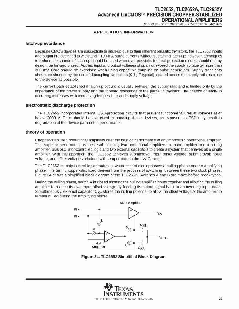
theory of operation
Chopper-stabilized operational amplifiers offer the best dc performance of any monolithic operational amplifier.This superior performance is the result of using two operational amplifiers, a main amplifier and a nullingamplifier, plus oscillator-controlled logic and two external capacitors to create a system that behaves as a singleamplifier. With this approach, the TLC2652 achieves submicrovolt input offset voltage, submicrovolt noisevoltage, and offset voltage variations with temperature in the nV/°C range.
The TLC2652 on-chip control logic produces two dominant clock phases: a nulling phase and an amplifyingphase. The term chopper-stabilized derives from the process of switching between these two clock phases.Figure 34 shows a simplified block diagram of the TLC2652. Switches A and B are make-before-break types.
During the nulling phase, switch A is closed shorting the nulling amplifier inputs together and allowing the nullingamplifier to reduce its own input offset voltage by feeding its output signal back to an inverting input node.Simultaneously, external capacitor CXA stores the nulling potential to allow the offset voltage of the amplifier toremain nulled during the amplifying phase.
NullAmplifier
IN+
IN−
Main Amplifier
VO
VDD−
CXA
CXBB
A
B
A
+
+
−
−
Figure 34. TLC2652 Simplified Block Diagram
SLOS019E − SEPTEMBER 1988 − REVISED FEBRUARY 2005
24 POST OFFICE BOX 655303 • DALLAS, TEXAS 75265
APPLICATION INFORMATION
theory of operation (continued)
During the amplifying phase, switch B is closed connecting the output of the nulling amplifier to a noninvertinginput of the main amplifier. In this configuration, the input offset voltage of the main amplifier is nulled. Also,external capacitor CXB stores the nulling potential to allow the offset voltage of the main amplifier to remainnulled during the next nulling phase.
This continuous chopping process allows offset voltage nulling during variations in time and temperature overthe common-mode input voltage range and power supply range. In addition, because the low-frequency signalpath is through both the null and main amplifiers, extremely high gain is achieved.
The low-frequency noise of a chopper amplifier depends on the magnitude of the component noise prior tochopping and the capability of the circuit to reduce this noise while chopping. The use of the Advanced LinCMOSprocess, with its low-noise analog MOS transistors and patent-pending input stage design, significantly reducesthe input noise voltage.
The primary source of nonideal operation in chopper-stabilized amplifiers is error charge from the switches. Ascharge imbalance accumulates on critical nodes, input offset voltage can increase, especially with increasingchopping frequency. This problem has been significantly reduced in the TLC2652 by use of a patent-pendingcompensation circuit and the Advanced LinCMOS process.
The TLC2652 incorporates a feed-forward design that ensures continuous frequency response. Essentially, thegain magnitude of the nulling amplifier and compensation network crosses unity at the break frequency of themain amplifier. As a result, the high-frequency response of the system is the same as the frequency responseof the main amplifier. This approach also ensures that the slewing characteristics remain the same during boththe nulling and amplifying phases.
PACKAGE OPTION ADDENDUM
www.ti.com 24-Aug-2018
Addendum-Page 1
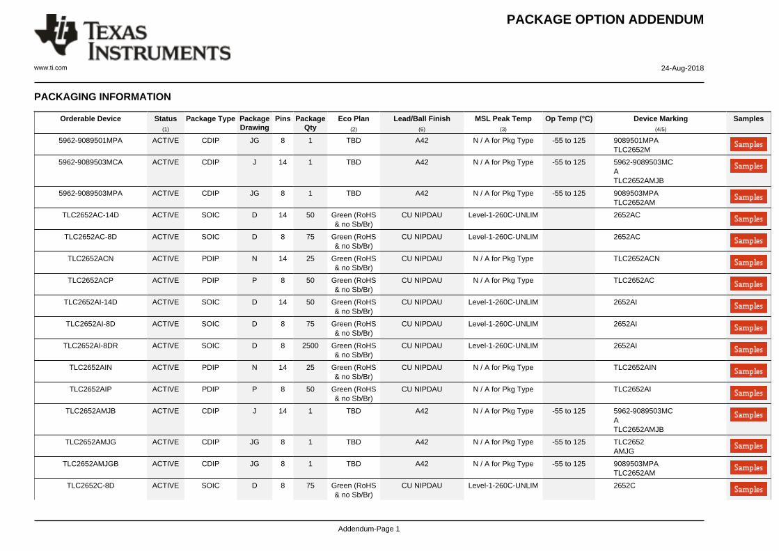
PACKAGING INFORMATION
Orderable Device Status(1)
Package Type PackageDrawing
Pins PackageQty
Eco Plan(2)
Lead/Ball Finish(6)
MSL Peak Temp(3)
Op Temp (°C) Device Marking(4/5)
Samples
5962-9089501MPA ACTIVE CDIP JG 8 1 TBD A42 N / A for Pkg Type -55 to 125 9089501MPATLC2652M
5962-9089503MCA ACTIVE CDIP J 14 1 TBD A42 N / A for Pkg Type -55 to 125 5962-9089503MCATLC2652AMJB
5962-9089503MPA ACTIVE CDIP JG 8 1 TBD A42 N / A for Pkg Type -55 to 125 9089503MPATLC2652AM
TLC2652AC-14D ACTIVE SOIC D 14 50 Green (RoHS& no Sb/Br)
CU NIPDAU Level-1-260C-UNLIM 2652AC
TLC2652AC-8D ACTIVE SOIC D 8 75 Green (RoHS& no Sb/Br)
CU NIPDAU Level-1-260C-UNLIM 2652AC
TLC2652ACN ACTIVE PDIP N 14 25 Green (RoHS& no Sb/Br)
CU NIPDAU N / A for Pkg Type TLC2652ACN
TLC2652ACP ACTIVE PDIP P 8 50 Green (RoHS& no Sb/Br)
CU NIPDAU N / A for Pkg Type TLC2652AC
TLC2652AI-14D ACTIVE SOIC D 14 50 Green (RoHS& no Sb/Br)
CU NIPDAU Level-1-260C-UNLIM 2652AI
TLC2652AI-8D ACTIVE SOIC D 8 75 Green (RoHS& no Sb/Br)
CU NIPDAU Level-1-260C-UNLIM 2652AI
TLC2652AI-8DR ACTIVE SOIC D 8 2500 Green (RoHS& no Sb/Br)
CU NIPDAU Level-1-260C-UNLIM 2652AI
TLC2652AIN ACTIVE PDIP N 14 25 Green (RoHS& no Sb/Br)
CU NIPDAU N / A for Pkg Type TLC2652AIN
TLC2652AIP ACTIVE PDIP P 8 50 Green (RoHS& no Sb/Br)
CU NIPDAU N / A for Pkg Type TLC2652AI
TLC2652AMJB ACTIVE CDIP J 14 1 TBD A42 N / A for Pkg Type -55 to 125 5962-9089503MCATLC2652AMJB
TLC2652AMJG ACTIVE CDIP JG 8 1 TBD A42 N / A for Pkg Type -55 to 125 TLC2652AMJG
TLC2652AMJGB ACTIVE CDIP JG 8 1 TBD A42 N / A for Pkg Type -55 to 125 9089503MPATLC2652AM
TLC2652C-8D ACTIVE SOIC D 8 75 Green (RoHS& no Sb/Br)
CU NIPDAU Level-1-260C-UNLIM 2652C
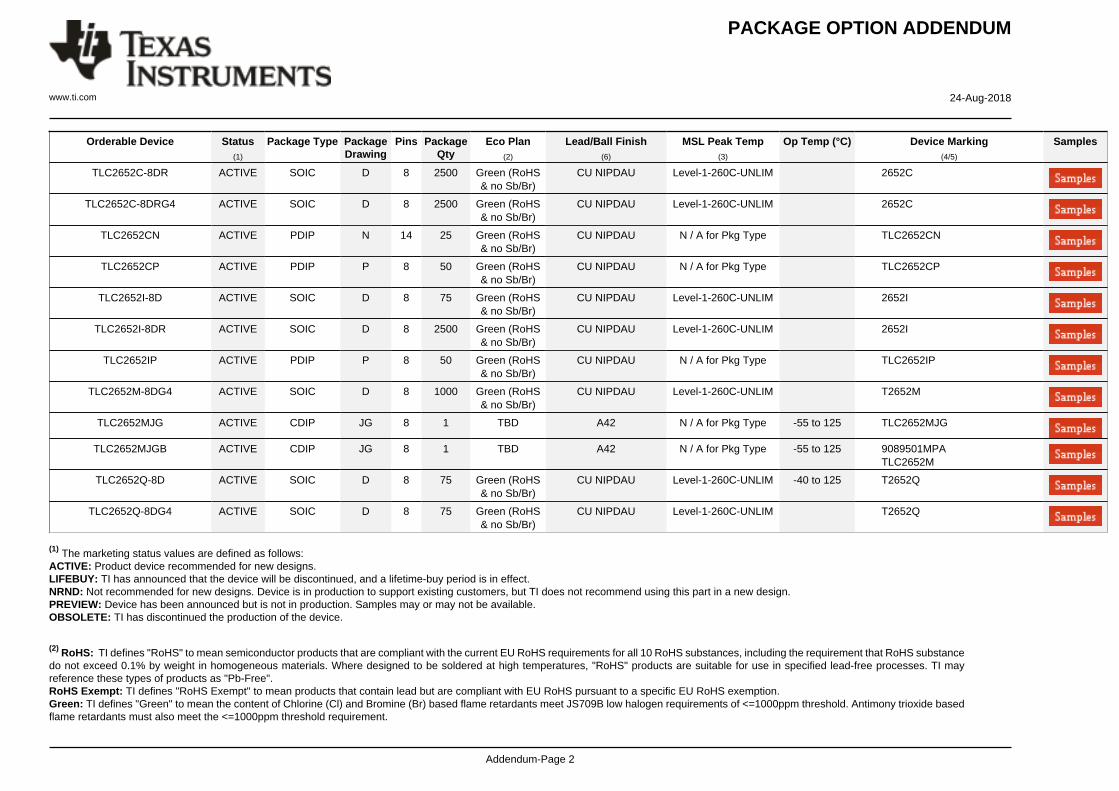
PACKAGE OPTION ADDENDUM
www.ti.com 24-Aug-2018
Addendum-Page 2
Orderable Device Status(1)
Package Type PackageDrawing
Pins PackageQty
Eco Plan(2)
Lead/Ball Finish(6)
MSL Peak Temp(3)
Op Temp (°C) Device Marking(4/5)
Samples
TLC2652C-8DR ACTIVE SOIC D 8 2500 Green (RoHS& no Sb/Br)
CU NIPDAU Level-1-260C-UNLIM 2652C
TLC2652C-8DRG4 ACTIVE SOIC D 8 2500 Green (RoHS& no Sb/Br)
CU NIPDAU Level-1-260C-UNLIM 2652C
TLC2652CN ACTIVE PDIP N 14 25 Green (RoHS& no Sb/Br)
CU NIPDAU N / A for Pkg Type TLC2652CN
TLC2652CP ACTIVE PDIP P 8 50 Green (RoHS& no Sb/Br)
CU NIPDAU N / A for Pkg Type TLC2652CP
TLC2652I-8D ACTIVE SOIC D 8 75 Green (RoHS& no Sb/Br)
CU NIPDAU Level-1-260C-UNLIM 2652I
TLC2652I-8DR ACTIVE SOIC D 8 2500 Green (RoHS& no Sb/Br)
CU NIPDAU Level-1-260C-UNLIM 2652I
TLC2652IP ACTIVE PDIP P 8 50 Green (RoHS& no Sb/Br)
CU NIPDAU N / A for Pkg Type TLC2652IP
TLC2652M-8DG4 ACTIVE SOIC D 8 1000 Green (RoHS& no Sb/Br)
CU NIPDAU Level-1-260C-UNLIM T2652M
TLC2652MJG ACTIVE CDIP JG 8 1 TBD A42 N / A for Pkg Type -55 to 125 TLC2652MJG
TLC2652MJGB ACTIVE CDIP JG 8 1 TBD A42 N / A for Pkg Type -55 to 125 9089501MPATLC2652M
TLC2652Q-8D ACTIVE SOIC D 8 75 Green (RoHS& no Sb/Br)
CU NIPDAU Level-1-260C-UNLIM -40 to 125 T2652Q
TLC2652Q-8DG4 ACTIVE SOIC D 8 75 Green (RoHS& no Sb/Br)
CU NIPDAU Level-1-260C-UNLIM T2652Q
(1) The marketing status values are defined as follows:ACTIVE: Product device recommended for new designs.LIFEBUY: TI has announced that the device will be discontinued, and a lifetime-buy period is in effect.NRND: Not recommended for new designs. Device is in production to support existing customers, but TI does not recommend using this part in a new design.PREVIEW: Device has been announced but is not in production. Samples may or may not be available.OBSOLETE: TI has discontinued the production of the device.
(2) RoHS: TI defines "RoHS" to mean semiconductor products that are compliant with the current EU RoHS requirements for all 10 RoHS substances, including the requirement that RoHS substancedo not exceed 0.1% by weight in homogeneous materials. Where designed to be soldered at high temperatures, "RoHS" products are suitable for use in specified lead-free processes. TI mayreference these types of products as "Pb-Free".RoHS Exempt: TI defines "RoHS Exempt" to mean products that contain lead but are compliant with EU RoHS pursuant to a specific EU RoHS exemption.Green: TI defines "Green" to mean the content of Chlorine (Cl) and Bromine (Br) based flame retardants meet JS709B low halogen requirements of <=1000ppm threshold. Antimony trioxide basedflame retardants must also meet the <=1000ppm threshold requirement.
PACKAGE OPTION ADDENDUM
www.ti.com 24-Aug-2018
Addendum-Page 3
(3) MSL, Peak Temp. - The Moisture Sensitivity Level rating according to the JEDEC industry standard classifications, and peak solder temperature.
(4) There may be additional marking, which relates to the logo, the lot trace code information, or the environmental category on the device.
(5) Multiple Device Markings will be inside parentheses. Only one Device Marking contained in parentheses and separated by a "~" will appear on a device. If a line is indented then it is a continuationof the previous line and the two combined represent the entire Device Marking for that device.
(6) Lead/Ball Finish - Orderable Devices may have multiple material finish options. Finish options are separated by a vertical ruled line. Lead/Ball Finish values may wrap to two lines if the finishvalue exceeds the maximum column width.
Important Information and Disclaimer:The information provided on this page represents TI's knowledge and belief as of the date that it is provided. TI bases its knowledge and belief on informationprovided by third parties, and makes no representation or warranty as to the accuracy of such information. Efforts are underway to better integrate information from third parties. TI has taken andcontinues to take reasonable steps to provide representative and accurate information but may not have conducted destructive testing or chemical analysis on incoming materials and chemicals.TI and TI suppliers consider certain information to be proprietary, and thus CAS numbers and other limited information may not be available for release.
In no event shall TI's liability arising out of such information exceed the total purchase price of the TI part(s) at issue in this document sold by TI to Customer on an annual basis.
OTHER QUALIFIED VERSIONS OF TLC2652, TLC2652A, TLC2652AM, TLC2652M :
• Catalog: TLC2652A, TLC2652
• Military: TLC2652M, TLC2652AM
NOTE: Qualified Version Definitions:
• Catalog - TI's standard catalog product
• Military - QML certified for Military and Defense Applications
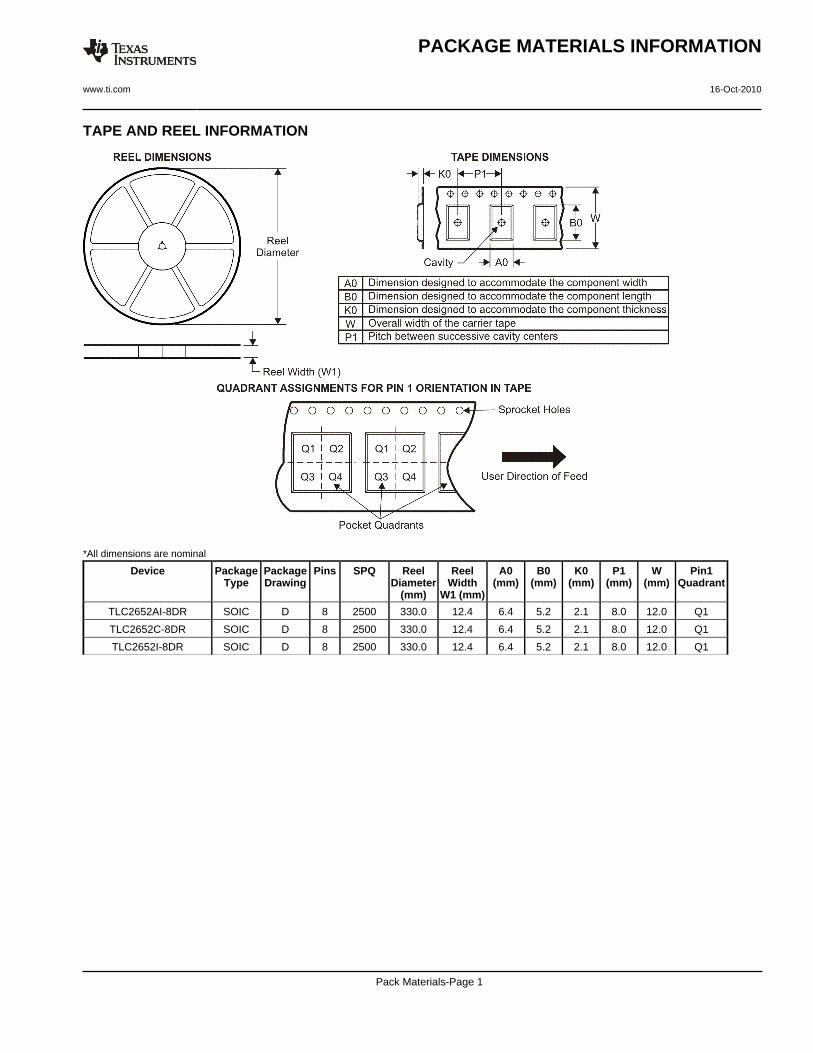
TAPE AND REEL INFORMATION
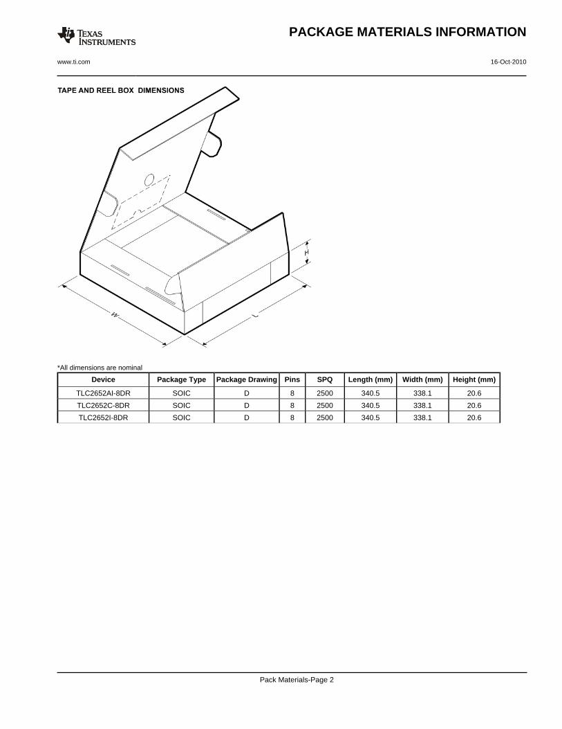
*All dimensions are nominal
Device PackageType
PackageDrawing
Pins SPQ ReelDiameter
(mm)
ReelWidth
W1 (mm)
A0(mm)
B0(mm)
K0(mm)
P1(mm)
W(mm)
Pin1Quadrant
TLC2652AI-8DR SOIC D 8 2500 330.0 12.4 6.4 5.2 2.1 8.0 12.0 Q1
TLC2652C-8DR SOIC D 8 2500 330.0 12.4 6.4 5.2 2.1 8.0 12.0 Q1
TLC2652I-8DR SOIC D 8 2500 330.0 12.4 6.4 5.2 2.1 8.0 12.0 Q1
PACKAGE MATERIALS INFORMATION
www.ti.com 16-Oct-2010
Pack Materials-Page 1
*All dimensions are nominal
Device Package Type Package Drawing Pins SPQ Length (mm) Width (mm) Height (mm)
TLC2652AI-8DR SOIC D 8 2500 340.5 338.1 20.6
TLC2652C-8DR SOIC D 8 2500 340.5 338.1 20.6
TLC2652I-8DR SOIC D 8 2500 340.5 338.1 20.6
PACKAGE MATERIALS INFORMATION
www.ti.com 16-Oct-2010
Pack Materials-Page 2
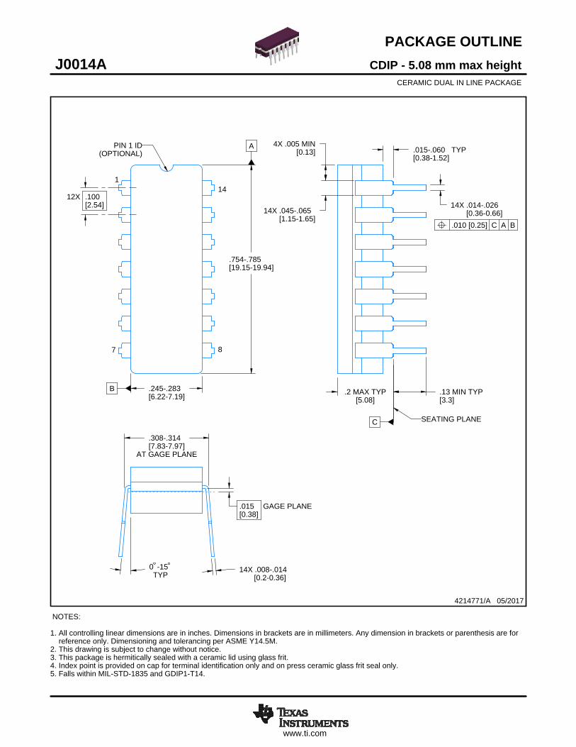
www.ti.com
PACKAGE OUTLINE
C
14X .008-.014 [0.2-0.36]TYP
-150
AT GAGE PLANE
-.314.308-7.977.83[ ]
14X -.026.014-0.660.36[ ]14X -.065.045
-1.651.15[ ]
.2 MAX TYP[5.08]
.13 MIN TYP[3.3]
TYP-.060.015-1.520.38[ ]
4X .005 MIN[0.13]
12X .100[2.54]
.015 GAGE PLANE[0.38]
A
-.785.754-19.9419.15[ ]
B -.283.245-7.196.22[ ]
CDIP - 5.08 mm max heightJ0014ACERAMIC DUAL IN LINE PACKAGE
4214771/A 05/2017
NOTES: 1. All controlling linear dimensions are in inches. Dimensions in brackets are in millimeters. Any dimension in brackets or parenthesis are for reference only. Dimensioning and tolerancing per ASME Y14.5M.2. This drawing is subject to change without notice. 3. This package is hermitically sealed with a ceramic lid using glass frit.4. Index point is provided on cap for terminal identification only and on press ceramic glass frit seal only.5. Falls within MIL-STD-1835 and GDIP1-T14.
7 8
141
PIN 1 ID(OPTIONAL)
SCALE 0.900
SEATING PLANE
.010 [0.25] C A B
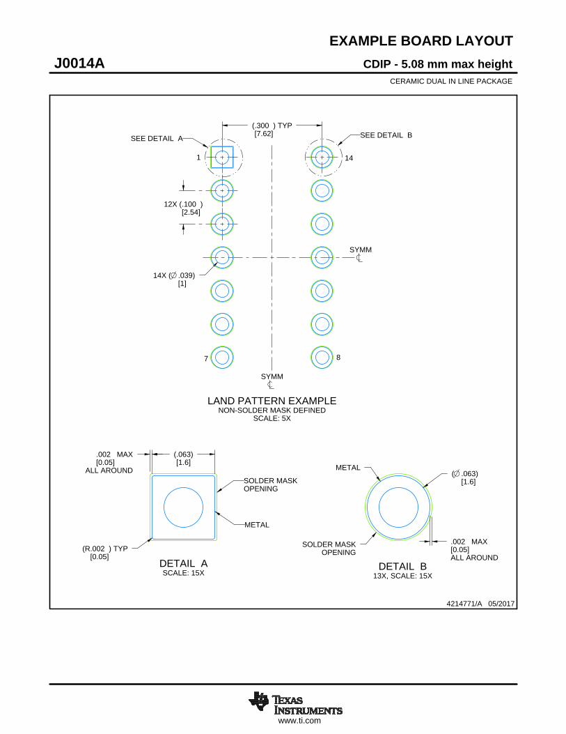
www.ti.com
EXAMPLE BOARD LAYOUT
ALL AROUND[0.05]
MAX.002
.002 MAX[0.05]ALL AROUND
SOLDER MASKOPENING
METAL
(.063)[1.6]
(R.002 ) TYP[0.05]
14X ( .039)[1]
( .063)[1.6]
12X (.100 )[2.54]
(.300 ) TYP[7.62]
CDIP - 5.08 mm max heightJ0014ACERAMIC DUAL IN LINE PACKAGE
4214771/A 05/2017
LAND PATTERN EXAMPLENON-SOLDER MASK DEFINED
SCALE: 5X
SEE DETAIL A SEE DETAIL B
SYMM
SYMM
1
7 8
14
DETAIL ASCALE: 15X
SOLDER MASKOPENING
METAL
DETAIL B13X, SCALE: 15X
MECHANICAL DATA
MCER001A – JANUARY 1995 – REVISED JANUARY 1997
POST OFFICE BOX 655303 • DALLAS, TEXAS 75265
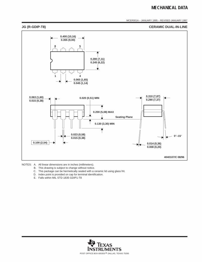
JG (R-GDIP-T8) CERAMIC DUAL-IN-LINE
0.310 (7,87)0.290 (7,37)
0.014 (0,36)0.008 (0,20)
Seating Plane
4040107/C 08/96
5
40.065 (1,65)0.045 (1,14)
8
1
0.020 (0,51) MIN
0.400 (10,16)0.355 (9,00)
0.015 (0,38)0.023 (0,58)
0.063 (1,60)0.015 (0,38)
0.200 (5,08) MAX
0.130 (3,30) MIN
0.245 (6,22)0.280 (7,11)
0.100 (2,54)
0°–15°
NOTES: A. All linear dimensions are in inches (millimeters).B. This drawing is subject to change without notice.C. This package can be hermetically sealed with a ceramic lid using glass frit.D. Index point is provided on cap for terminal identification.E. Falls within MIL STD 1835 GDIP1-T8
IMPORTANT NOTICE
Texas Instruments Incorporated (TI) reserves the right to make corrections, enhancements, improvements and other changes to itssemiconductor products and services per JESD46, latest issue, and to discontinue any product or service per JESD48, latest issue. Buyersshould obtain the latest relevant information before placing orders and should verify that such information is current and complete.TI’s published terms of sale for semiconductor products (http://www.ti.com/sc/docs/stdterms.htm) apply to the sale of packaged integratedcircuit products that TI has qualified and released to market. Additional terms may apply to the use or sale of other types of TI products andservices.Reproduction of significant portions of TI information in TI data sheets is permissible only if reproduction is without alteration and isaccompanied by all associated warranties, conditions, limitations, and notices. TI is not responsible or liable for such reproduceddocumentation. Information of third parties may be subject to additional restrictions. Resale of TI products or services with statementsdifferent from or beyond the parameters stated by TI for that product or service voids all express and any implied warranties for theassociated TI product or service and is an unfair and deceptive business practice. TI is not responsible or liable for any such statements.Buyers and others who are developing systems that incorporate TI products (collectively, “Designers”) understand and agree that Designersremain responsible for using their independent analysis, evaluation and judgment in designing their applications and that Designers havefull and exclusive responsibility to assure the safety of Designers' applications and compliance of their applications (and of all TI productsused in or for Designers’ applications) with all applicable regulations, laws and other applicable requirements. Designer represents that, withrespect to their applications, Designer has all the necessary expertise to create and implement safeguards that (1) anticipate dangerousconsequences of failures, (2) monitor failures and their consequences, and (3) lessen the likelihood of failures that might cause harm andtake appropriate actions. Designer agrees that prior to using or distributing any applications that include TI products, Designer willthoroughly test such applications and the functionality of such TI products as used in such applications.TI’s provision of technical, application or other design advice, quality characterization, reliability data or other services or information,including, but not limited to, reference designs and materials relating to evaluation modules, (collectively, “TI Resources”) are intended toassist designers who are developing applications that incorporate TI products; by downloading, accessing or using TI Resources in anyway, Designer (individually or, if Designer is acting on behalf of a company, Designer’s company) agrees to use any particular TI Resourcesolely for this purpose and subject to the terms of this Notice.TI’s provision of TI Resources does not expand or otherwise alter TI’s applicable published warranties or warranty disclaimers for TIproducts, and no additional obligations or liabilities arise from TI providing such TI Resources. TI reserves the right to make corrections,enhancements, improvements and other changes to its TI Resources. TI has not conducted any testing other than that specificallydescribed in the published documentation for a particular TI Resource.Designer is authorized to use, copy and modify any individual TI Resource only in connection with the development of applications thatinclude the TI product(s) identified in such TI Resource. NO OTHER LICENSE, EXPRESS OR IMPLIED, BY ESTOPPEL OR OTHERWISETO ANY OTHER TI INTELLECTUAL PROPERTY RIGHT, AND NO LICENSE TO ANY TECHNOLOGY OR INTELLECTUAL PROPERTYRIGHT OF TI OR ANY THIRD PARTY IS GRANTED HEREIN, including but not limited to any patent right, copyright, mask work right, orother intellectual property right relating to any combination, machine, or process in which TI products or services are used. Informationregarding or referencing third-party products or services does not constitute a license to use such products or services, or a warranty orendorsement thereof. Use of TI Resources may require a license from a third party under the patents or other intellectual property of thethird party, or a license from TI under the patents or other intellectual property of TI.TI RESOURCES ARE PROVIDED “AS IS” AND WITH ALL FAULTS. TI DISCLAIMS ALL OTHER WARRANTIES ORREPRESENTATIONS, EXPRESS OR IMPLIED, REGARDING RESOURCES OR USE THEREOF, INCLUDING BUT NOT LIMITED TOACCURACY OR COMPLETENESS, TITLE, ANY EPIDEMIC FAILURE WARRANTY AND ANY IMPLIED WARRANTIES OFMERCHANTABILITY, FITNESS FOR A PARTICULAR PURPOSE, AND NON-INFRINGEMENT OF ANY THIRD PARTY INTELLECTUALPROPERTY RIGHTS. TI SHALL NOT BE LIABLE FOR AND SHALL NOT DEFEND OR INDEMNIFY DESIGNER AGAINST ANY CLAIM,INCLUDING BUT NOT LIMITED TO ANY INFRINGEMENT CLAIM THAT RELATES TO OR IS BASED ON ANY COMBINATION OFPRODUCTS EVEN IF DESCRIBED IN TI RESOURCES OR OTHERWISE. IN NO EVENT SHALL TI BE LIABLE FOR ANY ACTUAL,DIRECT, SPECIAL, COLLATERAL, INDIRECT, PUNITIVE, INCIDENTAL, CONSEQUENTIAL OR EXEMPLARY DAMAGES INCONNECTION WITH OR ARISING OUT OF TI RESOURCES OR USE THEREOF, AND REGARDLESS OF WHETHER TI HAS BEENADVISED OF THE POSSIBILITY OF SUCH DAMAGES.Unless TI has explicitly designated an individual product as meeting the requirements of a particular industry standard (e.g., ISO/TS 16949and ISO 26262), TI is not responsible for any failure to meet such industry standard requirements.Where TI specifically promotes products as facilitating functional safety or as compliant with industry functional safety standards, suchproducts are intended to help enable customers to design and create their own applications that meet applicable functional safety standardsand requirements. Using products in an application does not by itself establish any safety features in the application. Designers mustensure compliance with safety-related requirements and standards applicable to their applications. Designer may not use any TI products inlife-critical medical equipment unless authorized officers of the parties have executed a special contract specifically governing such use.Life-critical medical equipment is medical equipment where failure of such equipment would cause serious bodily injury or death (e.g., lifesupport, pacemakers, defibrillators, heart pumps, neurostimulators, and implantables). Such equipment includes, without limitation, allmedical devices identified by the U.S. Food and Drug Administration as Class III devices and equivalent classifications outside the U.S.TI may expressly designate certain products as completing a particular qualification (e.g., Q100, Military Grade, or Enhanced Product).Designers agree that it has the necessary expertise to select the product with the appropriate qualification designation for their applicationsand that proper product selection is at Designers’ own risk. Designers are solely responsible for compliance with all legal and regulatoryrequirements in connection with such selection.Designer will fully indemnify TI and its representatives against any damages, costs, losses, and/or liabilities arising out of Designer’s non-compliance with the terms and provisions of this Notice.
Mailing Address: Texas Instruments, Post Office Box 655303, Dallas, Texas 75265Copyright © 2018, Texas Instruments Incorporated