Embed Size (px)
Citation preview
SLVS063E − NOVEMBER 1988 − REVISED OCTOBER 2003
1POST OFFICE BOX 655303 • DALLAS, TEXAS 75265
Low Temperature Coefficient
Wide Operating Current . . . 400 µAto 10 mA
0.27-Ω Dynamic Impedance
±1% Tolerance Available
Specified Temperature Stability
Easily Trimmed for Minimum TemperatureDrift
Fast Turnon
description/ordering information
The LM236-2.5, LM336-2.5, and LM336B-2.5integrated circuits are precision 2.5-V shuntregulator diodes. These reference circuitsoperate as low-temperature-coefficient 2.5-VZener diodes with a 0.2-Ω dynamic impedance. Athird terminal provided on the circuit allows thereference voltage and temperature coefficient tobe trimmed easily.
The series is useful as precision 2.5-V low-voltage references (VZ) for digital voltmeters, power supplies, oroperational-amplifier circuitry. The 2.5-V voltage reference makes it convenient to obtain a stable reference from5-V logic supplies. Devices in this series operate as shunt regulators, and can be used as either positive ornegative voltage references.
The LM236-2.5 is characterized for operation from −25°C to 85°C. The LM336-2.5 and LM336B-2.5 arecharacterized for operation from 0°C to 70°C.
ORDERING INFORMATION
TA PACKAGE † ORDERABLEPART NUMBER
TOP-SIDEMARKING
Tube of 75 LM336D-2-5336-25
SOIC (D)Reel of 2500 LM336DR-2-5
336-25
SOIC (D)Tube of 75 LM336BD-2-5
336B25
0°C to 70°CReel of 2500 LM336BDR−2-5
336B25
0°C to 70°CBulk of 1000 LM336LP-2-5
336-25
TO-226 / TO-92 (LP)Reel of 2000 LM336LPR-2-5
336-25
TO-226 / TO-92 (LP)Bulk of 1000 LM336BLP-2-5
336B25Reel of 2000 LM336BLPR-2-5
336B25
−25°C to 85°C SOIC (D)Tube of 75 LM236D-2-5
236-25−25°C to 85°C SOIC (D)Reel of 2500 LM236DR-2-5
236-25
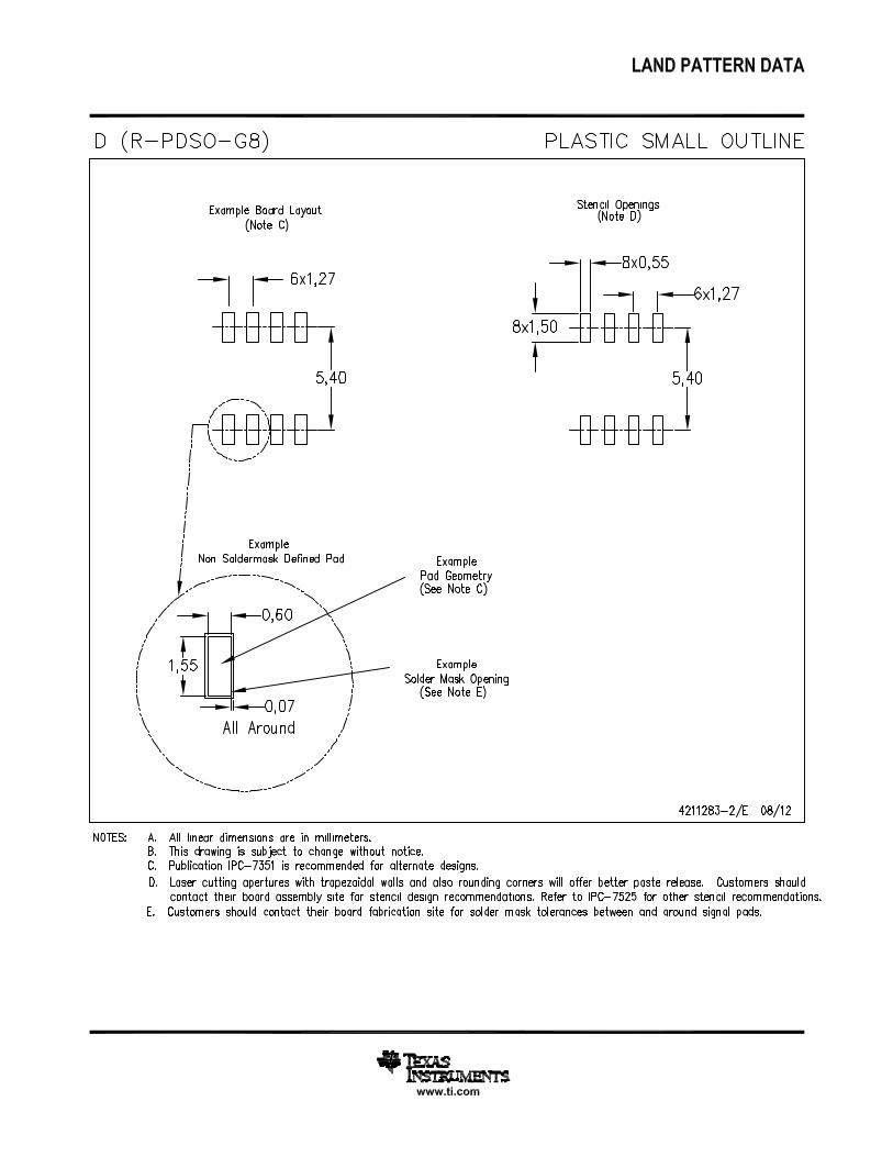
† Package drawings, standard packing quantities, thermal data, symbolization, and PCB design guidelines areavailable at www.ti.com/sc/package.
Copyright 2003, Texas Instruments Incorporated !" # $%&" !# '%()$!" *!"&*%$"# $ " #'&$$!"# '& "+& "&# &,!# #"%&"##"!*!* -!!". *%$" '$&##/ *&# " &$&##!). $)%*&"&#"/ !)) '!!&"&#
1
2
3
4
8
7
6
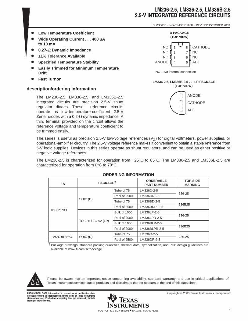
5
NCNCNC
ANODE
CATHODENCNCADJ
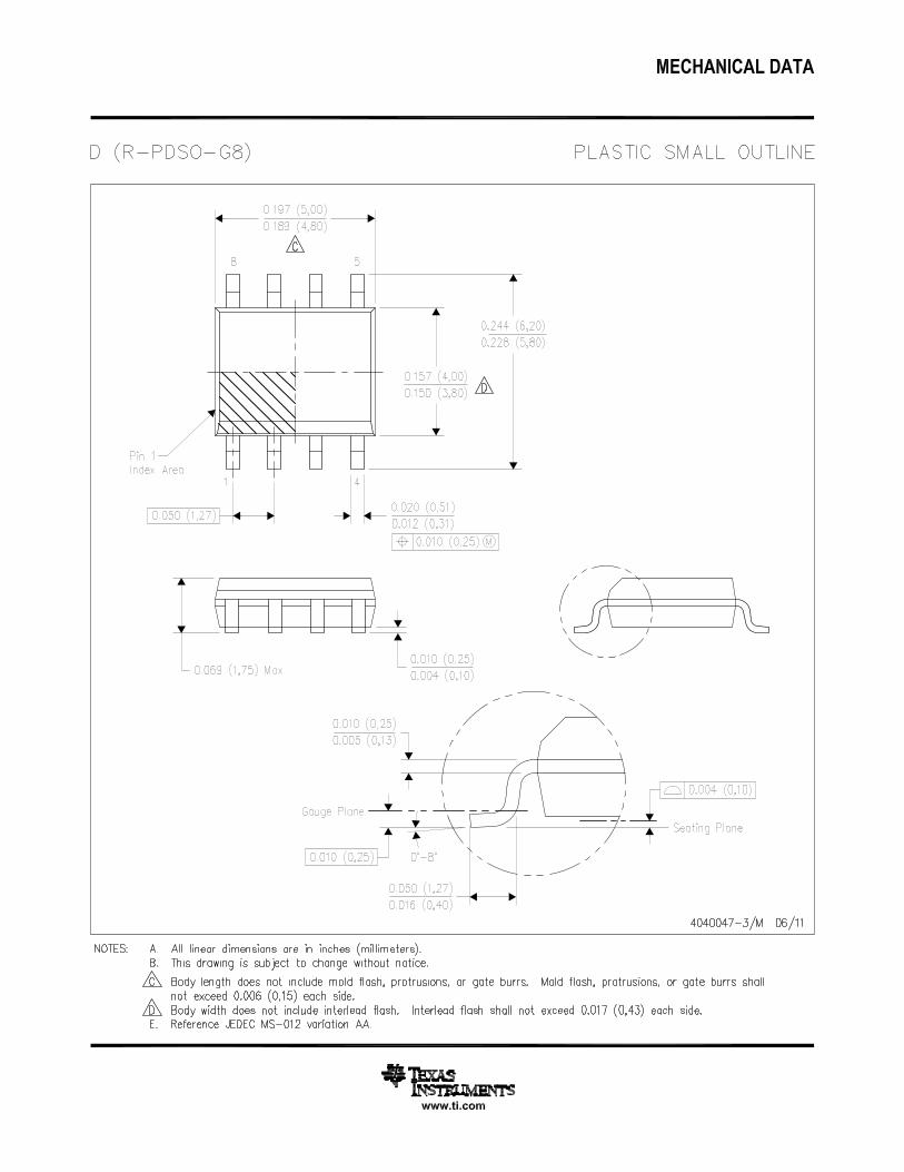
D PACKAGE(TOP VIEW)
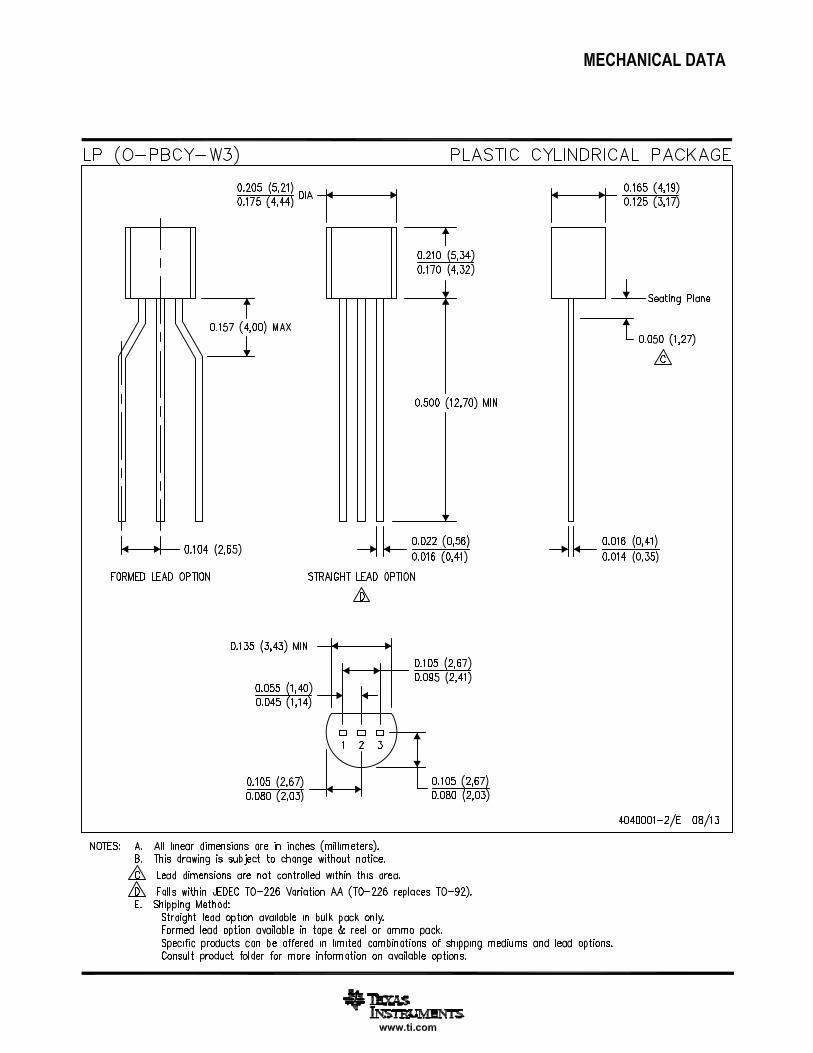
LM336-2.5, LM336B-2.5 . . . LP PACKAGE(TOP VIEW)
NC − No internal connection
ANODE
CATHODE
ADJ
Please be aware that an important notice concerning availability, standard warranty, and use in critical applications ofTexas Instruments semiconductor products and disclaimers thereto appears at the end of this data sheet.
SLVS063E − NOVEMBER 1988 − REVISED OCTOBER 2003
2 POST OFFICE BOX 655303 • DALLAS, TEXAS 75265
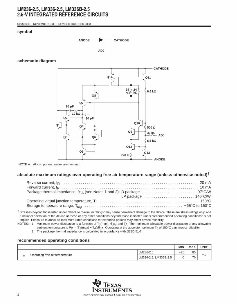
symbol
CATHODEANODE
ADJ
schematic diagram
CATHODE
Q11
6.6 kΩ24kΩ
24kΩ
Q14
Q8
Q7
Q2
20 pF
10 kΩ30 pF
Q10
Q3
Q1
Q5
Q4
Q6
Q9
Q12
Q13
500 Ω
30 kΩ
6.6 kΩ
720 Ω
ADJ
ANODE
NOTE A: All component values are nominal.
absolute maximum ratings over operating free-air temperature range (unless otherwise noted) †
Reverse current, IR 20 mA. . . . . . . . . . . . . . . . . . . . . . . . . . . . . . . . . . . . . . . . . . . . . . . . . . . . . . . . . . . . . . . . . . . . . . Forward current, IF 10 mA. . . . . . . . . . . . . . . . . . . . . . . . . . . . . . . . . . . . . . . . . . . . . . . . . . . . . . . . . . . . . . . . . . . . . . . Package thermal impedance, θJA (see Notes 1 and 2): D package 97°C/W. . . . . . . . . . . . . . . . . . . . . . . . . . . .
LP package 140°C/W. . . . . . . . . . . . . . . . . . . . . . . . . . Operating virtual junction temperature, TJ 150°C. . . . . . . . . . . . . . . . . . . . . . . . . . . . . . . . . . . . . . . . . . . . . . . . . . . Storage temperature range, Tstg −65°C to 150°C. . . . . . . . . . . . . . . . . . . . . . . . . . . . . . . . . . . . . . . . . . . . . . . . . . .
† Stresses beyond those listed under “absolute maximum ratings” may cause permanent damage to the device. These are stress ratings only, andfunctional operation of the device at these or any other conditions beyond those indicated under “recommended operating conditions” is notimplied. Exposure to absolute-maximum-rated conditions for extended periods may affect device reliability.
NOTES: 1. Maximum power dissipation is a function of TJ(max), θJA, and TA. The maximum allowable power dissipation at any allowableambient temperature is PD = (TJ(max) − TA)/θJA. Operating at the absolute maximum TJ of 150°C can impact reliability.
2. The package thermal impedance is calculated in accordance with JESD 51-7.
recommended operating conditionsMIN MAX UNIT
TA Operating free-air temperatureLM236-2.5 −25 85
°CTA Operating free-air temperatureLM336-2.5, LM336B-2.5 0 70
°C
SLVS063E − NOVEMBER 1988 − REVISED OCTOBER 2003
3POST OFFICE BOX 655303 • DALLAS, TEXAS 75265
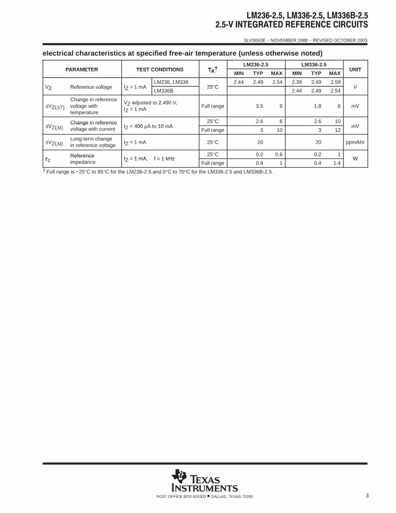
electrical characteristics at specified free-air temperature (unless otherwise noted)
PARAMETER TEST CONDITIONS TA†LM236-2.5 LM336-2.5
UNITPARAMETER TEST CONDITIONS TA†MIN TYP MAX MIN TYP MAX
UNIT
VZ Reference voltage IZ = 1 mALM236, LM336
25°C2.44 2.49 2.54 2.39 2.49 2.59
VVZ Reference voltage IZ = 1 mALM336B
25°C2.44 2.49 2.54
V
∆VZ(∆T)
Change in referencevoltage withtemperature
VZ adjusted to 2.490 V,IZ = 1 mA
Full range 3.5 9 1.8 6 mV
∆VZ( I)Change in reference
IZ = 400 A to 10 mA25°C 2.6 6 2.6 10
mV∆VZ(∆I)Change in referencevoltage with current IZ = 400 µA to 10 mA
Full range 3 10 3 12mV
∆VZ(∆t)Long-term changein reference voltage
IZ = 1 mA 25°C 20 20 ppm/khr
zzReference
IZ = 1 mA, f = 1 kHz25°C 0.2 0.6 0.2 1
WzzReferenceimpedance
IZ = 1 mA, f = 1 kHzFull range 0.4 1 0.4 1.4
W
† Full range is −25°C to 85°C for the LM236-2.5 and 0°C to 70°C for the LM336-2.5 and LM336B-2.5.
SLVS063E − NOVEMBER 1988 − REVISED OCTOBER 2003
4 POST OFFICE BOX 655303 • DALLAS, TEXAS 75265
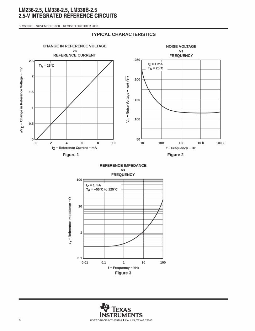
TYPICAL CHARACTERISTICS
Figure 1
∆V
−
Cha
nge
in R
efer
ence
Vol
tage
− m
VZ
1.5
1
0.5
00 2 4 6
2
CHANGE IN REFERENCE VOLTAGEvs
REFERENCE CURRENT
2.5
8 10IZ − Reference Current − mA
TA = 25°C
Figure 2
150
100
5010 100 1 k
200
f − Frequency − Hz
NOISE VOLTAGEvs
FREQUENCY250
10 k 100 k
IZ = 1 mATA = 25°C
− N
oise
Vol
tage
−V
nnV
/H
z
0.01 0.1 1
f − Frequency − kHz
10 100
REFERENCE IMPEDANCEvs
FREQUENCY
10
1
0.1
100
IZ = 1 mATA = −55°C to 125°C
Ωz z
− R
efer
ence
Impe
danc
e −
Figure 3
SLVS063E − NOVEMBER 1988 − REVISED OCTOBER 2003
5POST OFFICE BOX 655303 • DALLAS, TEXAS 75265
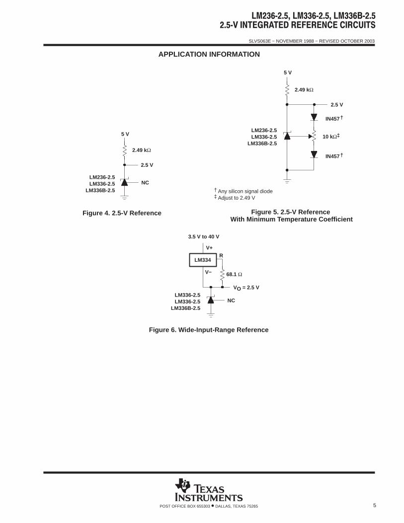
APPLICATION INFORMATION
2.49 kΩ
2.5 V
LM236-2.5LM336-2.5
LM336B-2.5
5 V
NC
Figure 4. 2.5-V Reference
2.49 kΩ
LM236-2.5LM336-2.5
LM336B-2.5
IN457†
IN457†
10 kه
5 V
† Any silicon signal diode‡ Adjust to 2.49 V
2.5 V
Figure 5. 2.5-V Reference With Minimum Temperature Coefficient
LM336-2.5LM336-2.5
LM336B-2.5
LM334
V+
V−
3.5 V to 40 V
68.1 Ω
VO = 2.5 V
R
NC
Figure 6. Wide-Input-Range Reference
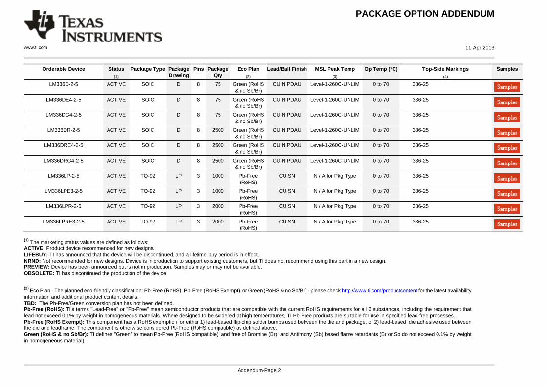
PACKAGE OPTION ADDENDUM
www.ti.com 11-Apr-2013
Addendum-Page 1
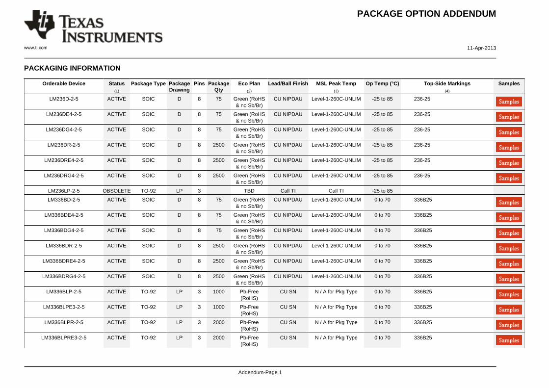
PACKAGING INFORMATION
Orderable Device Status(1)
Package Type PackageDrawing
Pins PackageQty
Eco Plan(2)
Lead/Ball Finish MSL Peak Temp(3)
Op Temp (°C) Top-Side Markings(4)
Samples
LM236D-2-5 ACTIVE SOIC D 8 75 Green (RoHS& no Sb/Br)
CU NIPDAU Level-1-260C-UNLIM -25 to 85 236-25
LM236DE4-2-5 ACTIVE SOIC D 8 75 Green (RoHS& no Sb/Br)
CU NIPDAU Level-1-260C-UNLIM -25 to 85 236-25
LM236DG4-2-5 ACTIVE SOIC D 8 75 Green (RoHS& no Sb/Br)
CU NIPDAU Level-1-260C-UNLIM -25 to 85 236-25
LM236DR-2-5 ACTIVE SOIC D 8 2500 Green (RoHS& no Sb/Br)
CU NIPDAU Level-1-260C-UNLIM -25 to 85 236-25
LM236DRE4-2-5 ACTIVE SOIC D 8 2500 Green (RoHS& no Sb/Br)
CU NIPDAU Level-1-260C-UNLIM -25 to 85 236-25
LM236DRG4-2-5 ACTIVE SOIC D 8 2500 Green (RoHS& no Sb/Br)
CU NIPDAU Level-1-260C-UNLIM -25 to 85 236-25
LM236LP-2-5 OBSOLETE TO-92 LP 3 TBD Call TI Call TI -25 to 85
LM336BD-2-5 ACTIVE SOIC D 8 75 Green (RoHS& no Sb/Br)
CU NIPDAU Level-1-260C-UNLIM 0 to 70 336B25
LM336BDE4-2-5 ACTIVE SOIC D 8 75 Green (RoHS& no Sb/Br)
CU NIPDAU Level-1-260C-UNLIM 0 to 70 336B25
LM336BDG4-2-5 ACTIVE SOIC D 8 75 Green (RoHS& no Sb/Br)
CU NIPDAU Level-1-260C-UNLIM 0 to 70 336B25
LM336BDR-2-5 ACTIVE SOIC D 8 2500 Green (RoHS& no Sb/Br)
CU NIPDAU Level-1-260C-UNLIM 0 to 70 336B25
LM336BDRE4-2-5 ACTIVE SOIC D 8 2500 Green (RoHS& no Sb/Br)
CU NIPDAU Level-1-260C-UNLIM 0 to 70 336B25
LM336BDRG4-2-5 ACTIVE SOIC D 8 2500 Green (RoHS& no Sb/Br)
CU NIPDAU Level-1-260C-UNLIM 0 to 70 336B25
LM336BLP-2-5 ACTIVE TO-92 LP 3 1000 Pb-Free(RoHS)
CU SN N / A for Pkg Type 0 to 70 336B25
LM336BLPE3-2-5 ACTIVE TO-92 LP 3 1000 Pb-Free(RoHS)
CU SN N / A for Pkg Type 0 to 70 336B25
LM336BLPR-2-5 ACTIVE TO-92 LP 3 2000 Pb-Free(RoHS)
CU SN N / A for Pkg Type 0 to 70 336B25
LM336BLPRE3-2-5 ACTIVE TO-92 LP 3 2000 Pb-Free(RoHS)
CU SN N / A for Pkg Type 0 to 70 336B25
PACKAGE OPTION ADDENDUM
www.ti.com 11-Apr-2013
Addendum-Page 2
Orderable Device Status(1)
Package Type PackageDrawing
Pins PackageQty
Eco Plan(2)
Lead/Ball Finish MSL Peak Temp(3)
Op Temp (°C) Top-Side Markings(4)
Samples
LM336D-2-5 ACTIVE SOIC D 8 75 Green (RoHS& no Sb/Br)
CU NIPDAU Level-1-260C-UNLIM 0 to 70 336-25
LM336DE4-2-5 ACTIVE SOIC D 8 75 Green (RoHS& no Sb/Br)
CU NIPDAU Level-1-260C-UNLIM 0 to 70 336-25
LM336DG4-2-5 ACTIVE SOIC D 8 75 Green (RoHS& no Sb/Br)
CU NIPDAU Level-1-260C-UNLIM 0 to 70 336-25
LM336DR-2-5 ACTIVE SOIC D 8 2500 Green (RoHS& no Sb/Br)
CU NIPDAU Level-1-260C-UNLIM 0 to 70 336-25
LM336DRE4-2-5 ACTIVE SOIC D 8 2500 Green (RoHS& no Sb/Br)
CU NIPDAU Level-1-260C-UNLIM 0 to 70 336-25
LM336DRG4-2-5 ACTIVE SOIC D 8 2500 Green (RoHS& no Sb/Br)
CU NIPDAU Level-1-260C-UNLIM 0 to 70 336-25
LM336LP-2-5 ACTIVE TO-92 LP 3 1000 Pb-Free(RoHS)
CU SN N / A for Pkg Type 0 to 70 336-25
LM336LPE3-2-5 ACTIVE TO-92 LP 3 1000 Pb-Free(RoHS)
CU SN N / A for Pkg Type 0 to 70 336-25
LM336LPR-2-5 ACTIVE TO-92 LP 3 2000 Pb-Free(RoHS)
CU SN N / A for Pkg Type 0 to 70 336-25
LM336LPRE3-2-5 ACTIVE TO-92 LP 3 2000 Pb-Free(RoHS)
CU SN N / A for Pkg Type 0 to 70 336-25
(1) The marketing status values are defined as follows:ACTIVE: Product device recommended for new designs.LIFEBUY: TI has announced that the device will be discontinued, and a lifetime-buy period is in effect.NRND: Not recommended for new designs. Device is in production to support existing customers, but TI does not recommend using this part in a new design.PREVIEW: Device has been announced but is not in production. Samples may or may not be available.OBSOLETE: TI has discontinued the production of the device.
(2) Eco Plan - The planned eco-friendly classification: Pb-Free (RoHS), Pb-Free (RoHS Exempt), or Green (RoHS & no Sb/Br) - please check http://www.ti.com/productcontent for the latest availabilityinformation and additional product content details.TBD: The Pb-Free/Green conversion plan has not been defined.Pb-Free (RoHS): TI's terms "Lead-Free" or "Pb-Free" mean semiconductor products that are compatible with the current RoHS requirements for all 6 substances, including the requirement thatlead not exceed 0.1% by weight in homogeneous materials. Where designed to be soldered at high temperatures, TI Pb-Free products are suitable for use in specified lead-free processes.Pb-Free (RoHS Exempt): This component has a RoHS exemption for either 1) lead-based flip-chip solder bumps used between the die and package, or 2) lead-based die adhesive used betweenthe die and leadframe. The component is otherwise considered Pb-Free (RoHS compatible) as defined above.Green (RoHS & no Sb/Br): TI defines "Green" to mean Pb-Free (RoHS compatible), and free of Bromine (Br) and Antimony (Sb) based flame retardants (Br or Sb do not exceed 0.1% by weightin homogeneous material)
PACKAGE OPTION ADDENDUM
www.ti.com 11-Apr-2013
Addendum-Page 3
(3) MSL, Peak Temp. -- The Moisture Sensitivity Level rating according to the JEDEC industry standard classifications, and peak solder temperature.
(4) Multiple Top-Side Markings will be inside parentheses. Only one Top-Side Marking contained in parentheses and separated by a "~" will appear on a device. If a line is indented then it is acontinuation of the previous line and the two combined represent the entire Top-Side Marking for that device.
Important Information and Disclaimer:The information provided on this page represents TI's knowledge and belief as of the date that it is provided. TI bases its knowledge and belief on informationprovided by third parties, and makes no representation or warranty as to the accuracy of such information. Efforts are underway to better integrate information from third parties. TI has taken andcontinues to take reasonable steps to provide representative and accurate information but may not have conducted destructive testing or chemical analysis on incoming materials and chemicals.TI and TI suppliers consider certain information to be proprietary, and thus CAS numbers and other limited information may not be available for release.
In no event shall TI's liability arising out of such information exceed the total purchase price of the TI part(s) at issue in this document sold by TI to Customer on an annual basis.
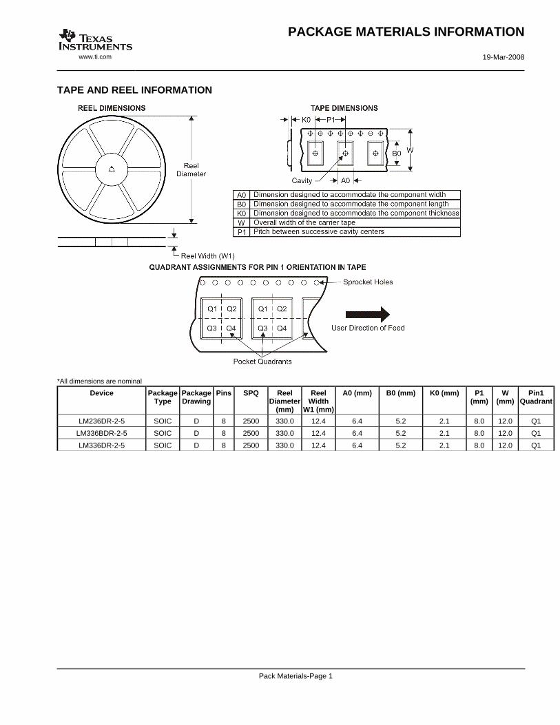
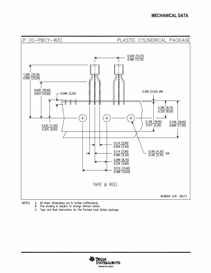
TAPE AND REEL INFORMATION
*All dimensions are nominal
Device PackageType
PackageDrawing
Pins SPQ ReelDiameter
(mm)
ReelWidth
W1 (mm)
A0 (mm) B0 (mm) K0 (mm) P1(mm)
W(mm)
Pin1Quadrant
LM236DR-2-5 SOIC D 8 2500 330.0 12.4 6.4 5.2 2.1 8.0 12.0 Q1
LM336BDR-2-5 SOIC D 8 2500 330.0 12.4 6.4 5.2 2.1 8.0 12.0 Q1
LM336DR-2-5 SOIC D 8 2500 330.0 12.4 6.4 5.2 2.1 8.0 12.0 Q1
PACKAGE MATERIALS INFORMATION
www.ti.com 19-Mar-2008
Pack Materials-Page 1
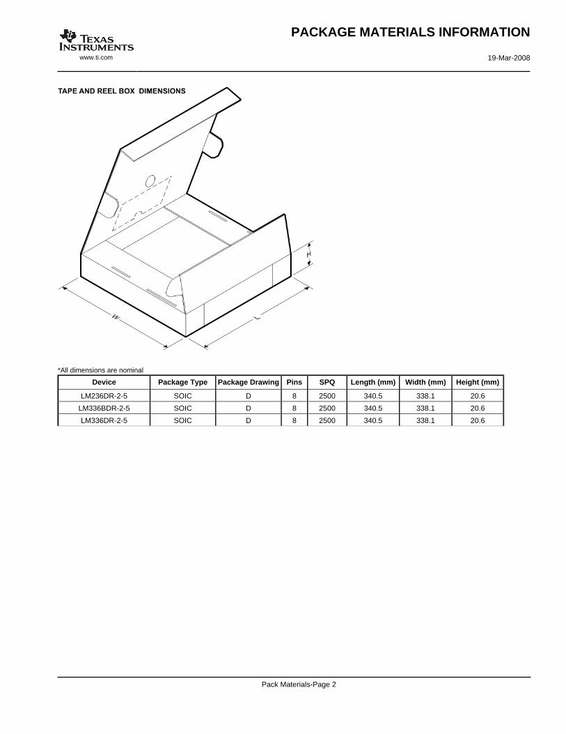
*All dimensions are nominal
Device Package Type Package Drawing Pins SPQ Length (mm) Width (mm) Height (mm)
LM236DR-2-5 SOIC D 8 2500 340.5 338.1 20.6
LM336BDR-2-5 SOIC D 8 2500 340.5 338.1 20.6
LM336DR-2-5 SOIC D 8 2500 340.5 338.1 20.6
PACKAGE MATERIALS INFORMATION
www.ti.com 19-Mar-2008
Pack Materials-Page 2
IMPORTANT NOTICE
Texas Instruments Incorporated and its subsidiaries (TI) reserve the right to make corrections, enhancements, improvements and otherchanges to its semiconductor products and services per JESD46, latest issue, and to discontinue any product or service per JESD48, latestissue. Buyers should obtain the latest relevant information before placing orders and should verify that such information is current andcomplete. All semiconductor products (also referred to herein as “components”) are sold subject to TI’s terms and conditions of salesupplied at the time of order acknowledgment.
TI warrants performance of its components to the specifications applicable at the time of sale, in accordance with the warranty in TI’s termsand conditions of sale of semiconductor products. Testing and other quality control techniques are used to the extent TI deems necessaryto support this warranty. Except where mandated by applicable law, testing of all parameters of each component is not necessarilyperformed.
TI assumes no liability for applications assistance or the design of Buyers’ products. Buyers are responsible for their products andapplications using TI components. To minimize the risks associated with Buyers’ products and applications, Buyers should provideadequate design and operating safeguards.
TI does not warrant or represent that any license, either express or implied, is granted under any patent right, copyright, mask work right, orother intellectual property right relating to any combination, machine, or process in which TI components or services are used. Informationpublished by TI regarding third-party products or services does not constitute a license to use such products or services or a warranty orendorsement thereof. Use of such information may require a license from a third party under the patents or other intellectual property of thethird party, or a license from TI under the patents or other intellectual property of TI.
Reproduction of significant portions of TI information in TI data books or data sheets is permissible only if reproduction is without alterationand is accompanied by all associated warranties, conditions, limitations, and notices. TI is not responsible or liable for such altereddocumentation. Information of third parties may be subject to additional restrictions.
Resale of TI components or services with statements different from or beyond the parameters stated by TI for that component or servicevoids all express and any implied warranties for the associated TI component or service and is an unfair and deceptive business practice.TI is not responsible or liable for any such statements.
Buyer acknowledges and agrees that it is solely responsible for compliance with all legal, regulatory and safety-related requirementsconcerning its products, and any use of TI components in its applications, notwithstanding any applications-related information or supportthat may be provided by TI. Buyer represents and agrees that it has all the necessary expertise to create and implement safeguards whichanticipate dangerous consequences of failures, monitor failures and their consequences, lessen the likelihood of failures that might causeharm and take appropriate remedial actions. Buyer will fully indemnify TI and its representatives against any damages arising out of the useof any TI components in safety-critical applications.
In some cases, TI components may be promoted specifically to facilitate safety-related applications. With such components, TI’s goal is tohelp enable customers to design and create their own end-product solutions that meet applicable functional safety standards andrequirements. Nonetheless, such components are subject to these terms.
No TI components are authorized for use in FDA Class III (or similar life-critical medical equipment) unless authorized officers of the partieshave executed a special agreement specifically governing such use.
Only those TI components which TI has specifically designated as military grade or “enhanced plastic” are designed and intended for use inmilitary/aerospace applications or environments. Buyer acknowledges and agrees that any military or aerospace use of TI componentswhich have not been so designated is solely at the Buyer's risk, and that Buyer is solely responsible for compliance with all legal andregulatory requirements in connection with such use.
TI has specifically designated certain components as meeting ISO/TS16949 requirements, mainly for automotive use. In any case of use ofnon-designated products, TI will not be responsible for any failure to meet ISO/TS16949.
Products Applications
Audio www.ti.com/audio Automotive and Transportation www.ti.com/automotive
Amplifiers amplifier.ti.com Communications and Telecom www.ti.com/communications
Data Converters dataconverter.ti.com Computers and Peripherals www.ti.com/computers
DLP® Products www.dlp.com Consumer Electronics www.ti.com/consumer-apps
DSP dsp.ti.com Energy and Lighting www.ti.com/energy
Clocks and Timers www.ti.com/clocks Industrial www.ti.com/industrial
Interface interface.ti.com Medical www.ti.com/medical
Logic logic.ti.com Security www.ti.com/security
Power Mgmt power.ti.com Space, Avionics and Defense www.ti.com/space-avionics-defense
Microcontrollers microcontroller.ti.com Video and Imaging www.ti.com/video
RFID www.ti-rfid.com
OMAP Applications Processors www.ti.com/omap TI E2E Community e2e.ti.com
Wireless Connectivity www.ti.com/wirelessconnectivity
Mailing Address: Texas Instruments, Post Office Box 655303, Dallas, Texas 75265Copyright © 2013, Texas Instruments Incorporated