Embed Size (px)
Citation preview
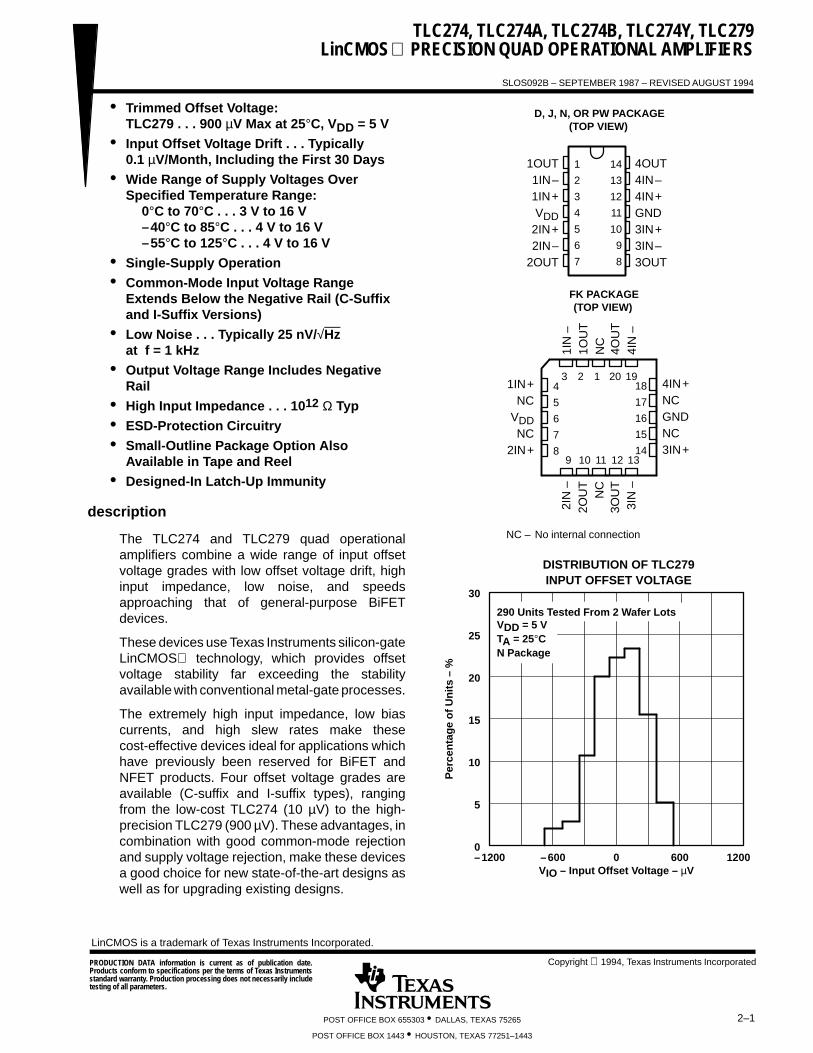
TLC274, TLC274A, TLC274B, TLC274Y, TLC279 LinCMOS PRECISION QUAD OPERATIONAL AMPLIFIERS
SLOS092B – SEPTEMBER 1987 – REVISED AUGUST 1994
Copyright 1994, Texas Instruments Incorporated
2–1POST OFFICE BOX 655303 • DALLAS, TEXAS 75265
POST OFFICE BOX 1443 • HOUSTON, TEXAS 77251–1443
• Trimmed Offset Voltage:TLC279 . . . 900 µV Max at 25°C, VDD = 5 V
• Input Offset Voltage Drif t . . . Typically0.1 µV/Month, Including the First 30 Days
• Wide Range of Supply Voltages OverSpecified Temperature Range:
0°C to 70°C . . . 3 V to 16 V–40°C to 85°C . . . 4 V to 16 V–55°C to 125°C . . . 4 V to 16 V
• Single-Supply Operation
• Common-Mode Input Voltage RangeExtends Below the Negative Rail (C-Suffixand I-Suffix Versions)
• Low Nois e . . . Typically 25 nV/ √Hzat f = 1 kHz
• Output Voltage Range Includes NegativeRail
• High Input Impedanc e . . . 1012 Ω Typ
• ESD-Protection Circuitry
• Small-Outline Package Option AlsoAvailable in Tape and Reel
• Designed-In Latch-Up Immunity
description
The TLC274 and TLC279 quad operationalamplifiers combine a wide range of input offsetvoltage grades with low offset voltage drift, highinput impedance, low noise, and speedsapproaching that of general-purpose BiFETdevices.
These devices use Texas Instruments silicon-gateLinCMOS technology, which provides offsetvoltage stability far exceeding the stabilityavailable with conventional metal-gate processes.
The extremely high input impedance, low biascurrents, and high slew rates make thesecost-effective devices ideal for applications whichhave previously been reserved for BiFET andNFET products. Four offset voltage grades areavailable (C-suffix and I-suffix types), rangingfrom the low-cost TLC274 (10 µV) to the high-precision TLC279 (900 µV). These advantages, incombination with good common-mode rejectionand supply voltage rejection, make these devicesa good choice for new state-of-the-art designs aswell as for upgrading existing designs.
–1200
Per
cent
age
of U
nits
– %
VIO – Input Offset Voltage – µV
30
12000
–600 0 600
5
10
15
20
25VDD = 5 VTA = 25°CN Package
DISTRIBUTION OF TLC279INPUT OFFSET VOLTAGE
1
2
3
4
5
6
7
14
13
12
11
10
9
8
1OUT1IN–1IN+VDD
2IN+2IN–
2OUT
4OUT4IN–4IN+GND3IN+3IN–3OUT
D, J, N, OR PW PACKAGE(TOP VIEW)
3 2 1 20 19
9 10 11 12 13
4
5
6
7
8
18
17
16
15
14
4IN+NCGNDNC3IN+
1IN+NC
VDDNC
2IN+
FK PACKAGE(TOP VIEW)
1IN
–1O
UT
NC
3OU
T3I
N –
4OU
T4I
N –
2IN
–2O
UT
NC
NC – No internal connection
290 Units Tested From 2 Wafer Lots
PRODUCTION DATA information is current as of publication date.Products conform to specifications per the terms of Texas Instrumentsstandard warranty. Production processing does not necessarily includetesting of all parameters.
LinCMOS is a trademark of Texas Instruments Incorporated.

TLC274, TLC274A, TLC274B, TLC274Y, TLC279LinCMOS PRECISION QUAD OPERATIONAL AMPLIFIERS
SLOS092B – SEPTEMBER 1987 – REVISED AUGUST 1994
2–2 POST OFFICE BOX 655303 • DALLAS, TEXAS 75265POST OFFICE BOX 1443 • HOUSTON, TEXAS 77251–1443
description (continued)
In general, many features associated with bipolar technology are available on LinCMOS operationalamplifiers, without the power penalties of bipolar technology. General applications such as transducerinterfacing, analog calculations, amplifier blocks, active filters, and signal buffering are easily designed with theTLC274 and TLC279. The devices also exhibit low voltage single-supply operation, making them ideally suitedfor remote and inaccessible battery-powered applications. The common-mode input voltage range includes thenegative rail.
A wide range of packaging options is available, including small-outline and chip-carrier versions for high-densitysystem applications.
The device inputs and outputs are designed to withstand –100-mA surge currents without sustaining latch-up.
The TLC274 and TLC279 incorporate internal ESD-protection circuits that prevent functional failures at voltagesup to 2000 V as tested under MIL-STD-883C, Method 3015.2; however, care should be exercised in handlingthese devices as exposure to ESD may result in the degradation of the device parametric performance.
The C-suffix devices are characterized for operation from 0°C to 70°C. The I-suffix devices are characterizedfor operation from –40°C to 85°C. The M-suffix devices are characterized for operation over the full militarytemperature range of –55°C to 125°C.
AVAILABLE OPTIONS
TV
PACKAGED DEVICESCHIP
TAVIOmaxAT 25°C
SMALL OUTLINE
(D)
CHIPCARRIER
(FK)
CERAMICDIP(J)
PLASTIC DIP(N)
TSSOP(PW)
CHIPFORM
(Y)
0°C to 70°C
900 µV2 mV5 mV
10 mV
TLC279CDTLC274BCDTLC274ACDTLC274CD
————
————
TLC279CNTLC274BCNTLC274ACNTLC274CN
———
TLC274CPW
———
TLC274Y
40°C 85°C
900 µV TLC279ID — — TLC279IN — —
–40°C to 85°C
900 µV2 mV
TLC279IDTLC274BID
——
——
TLC279INTLC274BIN
——
——–40°C to 85°C 2 mV
5 mVTLC274BIDTLC274AID — —
TLC274BINTLC274AIN — —
10 mV TLC274ID — — TLC274IN — —
–55°C to 125°C900 µV10 mV
TLC279MDTLC274MD
TLC279MFKTLC274MFK
TLC279MJTLC274MJ
TLC279MNTLC274MN
——
——
The D package is available taped and reeled. Add R suffix to the device type (e.g., TLC279CDR).

TLC274, TLC274A, TLC274B, TLC274Y, TLC279 LinCMOS PRECISION QUAD OPERATIONAL AMPLIFIERS
SLOS092B – SEPTEMBER 1987 – REVISED AUGUST 1994
2–3POST OFFICE BOX 655303 • DALLAS, TEXAS 75265POST OFFICE BOX 1443 • HOUSTON, TEXAS 77251–1443
equivalent schematic (each amplifier)
VDD
P4P3
R6
N5R2
P2
R1
P1
IN–
IN+
N1
R3 D1 R4 D2
N2
GND
N3
R5C1
N4
R7
N6 N7
OUT
P6P5

TLC274, TLC274A, TLC274B, TLC274Y, TLC279LinCMOS PRECISION QUAD OPERATIONAL AMPLIFIERS
SLOS092B – SEPTEMBER 1987 – REVISED AUGUST 1994
2–4 POST OFFICE BOX 655303 • DALLAS, TEXAS 75265POST OFFICE BOX 1443 • HOUSTON, TEXAS 77251–1443
TLC274Y chip information
These chips, when properly assembled, display characteristics similar to the TLC274C. Thermal compressionor ultrasonic bonding may be used on the doped-aluminum bonding pads. Chips may be mounted withconductive epoxy or a gold-silicon preform.
BONDING PAD ASSIGNMENTS
CHIP THICKNESS: 15 TYPICAL
BONDING PADS: 4 × 4 MINIMUM
TJmax = 150°C
TOLERANCES ARE ±10%.
ALL DIMENSIONS ARE IN MILS.
PIN (11) IS INTERNALLY CONNECTEDTO BACKSIDE OF CHIP.
+
–1OUT
1IN+
1IN–
VDD(4)
(6)
(3)
(2)
(5)
(1)
–
+(7) 2IN+
2IN–2OUT
11
GND
+
–3OUT
3IN+
3IN–
(13)
(10)
(9)
(12)
(8)
–
+(14)4OUT
4IN+
4IN–
68
108
(1) (2) (3) (4) (5) (6) (7)
(8)(9)(10)(11)(12)(13)(14)

TLC274, TLC274A, TLC274B, TLC274Y, TLC279 LinCMOS PRECISION QUAD OPERATIONAL AMPLIFIERS
SLOS092B – SEPTEMBER 1987 – REVISED AUGUST 1994
2–5POST OFFICE BOX 655303 • DALLAS, TEXAS 75265POST OFFICE BOX 1443 • HOUSTON, TEXAS 77251–1443
absolute maximum ratings over operating free-air temperature range (unless otherwise noted) †
Supply voltage, VDD (see Note 1) 18 V. . . . . . . . . . . . . . . . . . . . . . . . . . . . . . . . . . . . . . . . . . . . . . . . . . . . . . . . . . . Differential input voltage, VID (see Note 2) ±VDD. . . . . . . . . . . . . . . . . . . . . . . . . . . . . . . . . . . . . . . . . . . . . . . . . . Input voltage range, VI (any input) –0.3 V to VDD. . . . . . . . . . . . . . . . . . . . . . . . . . . . . . . . . . . . . . . . . . . . . . . . . . . Input current, II ±5 mA. . . . . . . . . . . . . . . . . . . . . . . . . . . . . . . . . . . . . . . . . . . . . . . . . . . . . . . . . . . . . . . . . . . . . . . . . . Output current, lO (each output) ±30 mA. . . . . . . . . . . . . . . . . . . . . . . . . . . . . . . . . . . . . . . . . . . . . . . . . . . . . . . . . Total current into VDD 45 mA. . . . . . . . . . . . . . . . . . . . . . . . . . . . . . . . . . . . . . . . . . . . . . . . . . . . . . . . . . . . . . . . . . . . Total current out of GND 45 mA. . . . . . . . . . . . . . . . . . . . . . . . . . . . . . . . . . . . . . . . . . . . . . . . . . . . . . . . . . . . . . . . . . Duration of short-circuit current at (or below) 25°C (see Note 3) unlimited. . . . . . . . . . . . . . . . . . . . . . . . . . . . . . Continuous total dissipation See Dissipation Rating Table. . . . . . . . . . . . . . . . . . . . . . . . . . . . . . . . . . . . . . . . . . . Operating free-air temperature, TA: C suffix 0°C to 70°C. . . . . . . . . . . . . . . . . . . . . . . . . . . . . . . . . . . . . . . . . . . .
I suffix –40°C to 85°C. . . . . . . . . . . . . . . . . . . . . . . . . . . . . . . . . . . . . . . . . . . M suffix –55°C to 125°C. . . . . . . . . . . . . . . . . . . . . . . . . . . . . . . . . . . . . . . .
Storage temperature range –65°C to 150°C. . . . . . . . . . . . . . . . . . . . . . . . . . . . . . . . . . . . . . . . . . . . . . . . . . . . . . . Case temperature for 60 seconds: FK package 260°C. . . . . . . . . . . . . . . . . . . . . . . . . . . . . . . . . . . . . . . . . . . . . . Lead temperature 1,6 mm (1/16 inch) from case for 10 seconds: D, N, or PW package 260°C. . . . . . . . . . . . Lead temperature 1,6 mm (1/16 inch) from case for 60 seconds: J package 300°C. . . . . . . . . . . . . . . . . . . . .
† Stresses beyond those listed under “absolute maximum ratings” may cause permanent damage to the device. These are stress ratings only, andfunctional operation of the device at these or any other conditions beyond those indicated under “recommended operating conditions” is notimplied. Exposure to absolute-maximum-rated conditions for extended periods may affect device reliability.
NOTES: 1. All voltage values, except differential voltages, are with respect to network ground.2. Differential voltages are at the noninverting input with respect to the inverting input.3. The output may be shorted to either supply. Temperature and/or supply voltages must be limited to ensure that the maximum
dissipation rating is not exceeded (see application section).
DISSIPATION RATING TABLE
PACKAGETA ≤ 25°C
POWER RATINGDERATING FACTORABOVE TA = 25°C
TA = 70°CPOWER RATING
TA = 85°CPOWER RATING
TA = 125°CPOWER RATING
D 950 mW 7.6 mW/°C 608 mW 494 mW —
FK 1375 mW 11.0 mW/°C 880 mW 715 mW 275 mW
J 1375 mW 11.0 mW/°C 880 mW 715 mW 275 mW
N 1575 mW 12.6 mW/°C 1008 mW 819 mW —
PW 700 mW 5.6 mW/°C 448 mW — —
recommended operating conditions
C SUFFIX I SUFFIX M SUFFIXUNIT
MIN MAX MIN MAX MIN MAXUNIT
Supply voltage, VDD 3 16 4 16 4 16 V
Common-mode input voltage VICVDD = 5 V –0.2 3.5 –0.2 3.5 0 3.5
VCommon-mode input voltage, VICVDD = 10 V –0.2 8.5 –0.2 8.5 0 8.5
V
Operating free-air temperature, TA 0 70 –40 85 –55 125 °C

TLC274, TLC274A, TLC274B, TLC274Y, TLC279LinCMOS PRECISION QUAD OPERATIONAL AMPLIFIERS
SLOS092B – SEPTEMBER 1987 – REVISED AUGUST 1994
2–6 POST OFFICE BOX 655303 • DALLAS, TEXAS 75265POST OFFICE BOX 1443 • HOUSTON, TEXAS 77251–1443
electrical characteristics at specified free-air temperature, V DD = 5 V (unless otherwise noted)
PARAMETER TEST CONDITIONS TA†TLC274C, TLC274AC,TLC274BC, TLC279C UNITPARAMETER TEST CONDITIONS TA
MIN TYP MAXUNIT
V I ff l
TLC274CVO = 1.4 V, VIC = 0, 25°C 1.1 10
V
V I ff l
TLC274CVO 1.4 V,RS = 50 Ω,
VIC 0,RL = 10 kΩ Full range 12
mV
V I ff l
TLC274ACVO = 1.4 V, VIC = 0, 25°C 0.9 5
mV
VIO Input offset voltage
TLC274ACVO 1.4 V,RS = 50 Ω,
VIC 0,RL = 10 kΩ Full range 6.5
VIO Input offset voltage
TLC274BCVO = 1.4 V, VIC = 0, 25°C 340 2000
V
TLC274BCVO 1.4 V,RS = 50 Ω,
VIC 0,RL = 10 kΩ Full range 3000
µV
TLC279CVO = 1.4 V, VIC = 0, 25°C 320 900
µV
TLC279CVO 1.4 V,RS = 50 Ω,
VIC 0,RL = 10 kΩ Full range 1500
αVIOAverage temperature coefficient of inputoffset voltage
25°C to 70°C 1.8 µV/°C
IIO Input offset current (see Note 4) VO = 2 5 V VIC = 2 5 V25°C 0.1
pAIIO Input offset current (see Note 4) VO = 2.5 V, VIC = 2.5 V70°C 7 300
pA
IIB Input bias current (see Note 4) VO = 2 5 V VIC = 2 5 V25°C 0.6
pAIIB Input bias current (see Note 4) VO = 2.5 V, VIC = 2.5 V70°C 40 600
pA
VICRCommon-mode input voltage range
25°C–0.2
to4
–0.3to
4.2V
VICRCommon mode input voltage range(see Note 5)
Full range–0.2
to3.5
V
V Hi h l l l V 100 V R 10 kΩ
25°C 3.2 3.8
VVOH High-level output voltage VID = 100 mV, RL = 10 kΩ 0°C 3 3.8 VOH g p g ID L70°C 3 3.8
V L l l l V 100 V I 0
25°C 0 50
VVOL Low-level output voltage VID = –100 mV, IOL = 0 0°C 0 50 mVOL p g ID OL70°C 0 50
ALarge signal differential voltage
V 0 25 V 2 V R 10 kΩ
25°C 5 23
V/ VAVDLarge-signal differential voltageamplification
VO = 0.25 V to 2 V, RL = 10 kΩ 0°C 4 27 V/mVVD amplification O L70°C 4 20
CMRR C d j i i V V i
25°C 65 80
dBCMRR Common-mode rejection ratio VIC = VICRmin 0°C 60 84 dBj IC ICR70°C 60 85
kSupply voltage rejection ratio
V 5 V 10 V V 1 4 V
25°C 65 95
dBkSVRSupply-voltage rejection ratio(∆VDD/∆VIO)
VDD = 5 V to 10 V, VO = 1.4 V 0°C 60 94 dBSVR (∆VDD/∆VIO) DD O70°C 60 96
I S l (f lifi )VO = 2 5 V VIC = 2 5 V
25°C 2.7 6.4
AIDD Supply current (four amplifiers)VO = 2.5 V,No load
VIC = 2.5 V,0°C 3.1 7.2 mADD pp y ( p ) No load
70°C 2.3 5.2
† Full range is 0°C to 70°C.NOTES: 4. The typical values of input bias current and input offset current below 5 pA were determined mathematically.
5. This range also applies to each input individually.

TLC274, TLC274A, TLC274B, TLC274Y, TLC279 LinCMOS PRECISION QUAD OPERATIONAL AMPLIFIERS
SLOS092B – SEPTEMBER 1987 – REVISED AUGUST 1994
2–7POST OFFICE BOX 655303 • DALLAS, TEXAS 75265POST OFFICE BOX 1443 • HOUSTON, TEXAS 77251–1443
electrical characteristics at specified free-air temperature, V DD = 10 V (unless otherwise noted)
PARAMETER TEST CONDITIONS TA†TLC274C, TLC274AC,TLC274BC, TLC279C UNITPARAMETER TEST CONDITIONS TA
MIN TYP MAXUNIT
V I ff l
TLC274CVO = 1.4 V, VIC = 0, 25°C 1.1 10
V
V I ff l
TLC274CVO 1.4 V,RS = 50 Ω,
VIC 0,RL = 10 kΩ Full range 12
mV
V I ff l
TLC274ACVO = 1.4 V, VIC = 0, 25°C 0.9 5
mV
VIO Input offset voltage
TLC274ACVO 1.4 V,RS = 50 Ω,
VIC 0,RL = 10 kΩ Full range 6.5
VIO Input offset voltage
TLC274BCVO = 1.4 V, VIC = 0, 25°C 390 2000
V
TLC274BCVO 1.4 V,RS = 50 Ω,
VIC 0,RL = 10 kΩ Full range 3000
µV
TLC279CVO = 1.4 V, VIC = 0, 25°C 370 1200
µV
TLC279CVO 1.4 V,RS = 50 Ω,
VIC 0,RL = 10 kΩ Full range 1900
αVIOAverage temperature coefficient of inputoffset voltage
25°C to 70°C 2 µV/°C
IIO Input offset current (see Note 4) VO = 5 V VIC = 5 V25°C 0.1
pAIIO Input offset current (see Note 4) VO =.5 V, VIC = 5 V70°C 7 300
pA
IIB Input bias current (see Note 4) VO = 5 V VIC = 5 V25°C 0.7
pAIIB Input bias current (see Note 4) VO = 5 V, VIC = 5 V70°C 50 600
pA
VICRCommon-mode input voltage range
25°C–0.2
to9
–0.3to
9.2V
VICRCommon mode input voltage range(see Note 5)
Full range–0.2
to8.5
V
V Hi h l l l V 100 V R 10 kΩ
25°C 8 8.5
VVOH High-level output voltage VID = 100 mV, RL = 10 kΩ 0°C 7.8 8.5 VOH g p g ID L70°C 7.8 8.4
V L l l l V 100 V I 0
25°C 0 50
VVOL Low-level output voltage VID = –100 mV, IOL = 0 0°C 0 50 mVOL p g ID OL70°C 0 50
ALarge signal differential voltage
V 1 V 6 V R 10 kΩ
25°C 10 36
V/ VAVDLarge-signal differential voltageamplification
VO = 1 V to 6 V, RL = 10 kΩ 0°C 7.5 42 V/mVVD amplification O L70°C 7.5 32
CMRR C d j i i V V i
25°C 65 85
dBCMRR Common-mode rejection ratio VIC = VICRmin 0°C 60 88 dBj IC ICR70°C 60 88
kSupply voltage rejection ratio
V 5 V 10 V V 1 4 V
25°C 65 95
dBkSVRSupply-voltage rejection ratio(∆VDD/∆VIO)
VDD = 5 V to 10 V, VO = 1.4 V 0°C 60 94 dBSVR (∆VDD/∆VIO) DD O70°C 60 96
I S l (f lifi )V 5 V V 5 V
25°C 3.8 8
AIDD Supply current (four amplifiers)VO = 5 V,No load
VIC = 5 V,0°C 4.5 8.8 mADD pp y ( p )
No load70°C 3.2 6.8
† Full range is 0°C to 70°C.NOTES: 4. The typical values of input bias current and input offset current below 5 pA were determined mathematically.
5. This range also applies to each input individually.

TLC274, TLC274A, TLC274B, TLC274Y, TLC279LinCMOS PRECISION QUAD OPERATIONAL AMPLIFIERS
SLOS092B – SEPTEMBER 1987 – REVISED AUGUST 1994
2–8 POST OFFICE BOX 655303 • DALLAS, TEXAS 75265POST OFFICE BOX 1443 • HOUSTON, TEXAS 77251–1443
electrical characteristics at specified free-air temperature, V DD = 5 V (unless otherwise noted)
PARAMETER TEST CONDITIONS TA†TLC274I, TLC274AI,TLC274BI, TLC279I UNITTAMIN TYP MAX
V I ff l
TLC274IVO = 1.4 V, VIC = 0, 25°C 1.1 10
V
V I ff l
TLC274I O ,RS = 50 Ω,
IC ,RL = 10 kΩ Full range 13
mV
V I ff l
TLC274AIVO = 1.4 V, VIC = 0, 25°C 0.9 5
mV
VIO Input offset voltage
TLC274AI O ,RS = 50 Ω,
IC ,RL = 10 kΩ Full range 7
VIO Input offset voltage
TLC274BIVO = 1.4 V, VIC = 0, 25°C 340 2000
V
TLC274BI O ,RS = 50 Ω,
IC ,RL = 10 kΩ Full range 3500
µV
TLC279IVO = 1.4 V, VIC = 0, 25°C 320 900
µV
TLC279I O ,RS = 50 Ω,
IC ,RL = 10 kΩ Full range 2000
αVIOAverage temperature coefficient of inputoffset voltage
25°C to 85°C 1.8 µV/°C
IIO Input offset current (see Note 4) VO = 2 5 V VIC = 2 5 V25°C 0.1
pAIIO Input offset current (see Note 4) VO = 2.5 V, VIC = 2.5 V85°C 24 1000
pA
IIB Input bias current (see Note 4) VO = 2 5 V VIC = 2 5 V25°C 0.6
pAIIB Input bias current (see Note 4) VO = 2.5 V, VIC = 2.5 V85°C 200 2000
pA
VICRCommon-mode input voltage range
25°C–0.2
to4
–0.3to
4.2V
VICRp g g
(see Note 5)Full range
–0.2to
3.5V
V Hi h l l l V 100 V R 10 kΩ25°C 3.2 3.8
VVOH High-level output voltage VID = 100 mV, RL = 10 kΩ –40°C 3 3.8 VOH g p g ID L85°C 3 3.8
V L l l l V 100 V I 0
25°C 0 50
VVOL Low-level output voltage VID = –100 mV, IOL = 0 –40°C 0 50 mVOL p g ID OL85°C 0 50
ALarge signal differential voltage
V 0 25 V 2 V R 10 kΩ25°C 5 23
V/ VAVDLarge-signal differential voltageamplification
VO = 0.25 V to 2 V, RL = 10 kΩ –40°C 3.5 32 V/mVVD amplification O L85°C 3.5 19
CMRR C d j i i V V i
25°C 65 80
dBCMRR Common-mode rejection ratio VIC = VICRmin –40°C 60 81 dBj IC ICR85°C 60 86
kSupply voltage rejection ratio
V 5 V 10 V V 1 4 V
25°C 65 95
dBkSVRSupply-voltage rejection ratio (∆VDD/∆VIO)
VDD = 5 V to 10 V, VO = 1.4 V –40°C 60 92 dBSVR (∆VDD/∆VIO) DD O85°C 60 96
I S l (f lifi )VO = 2 5 V VIC = 2 5 V
25°C 2.7 6.4
AIDD Supply current (four amplifiers)VO = 2.5 V,No load
VIC = 2.5 V,–40°C 3.8 8.8 mADD pp y ( p ) No load
85°C 2.1 4.8† Full range is –40°C to 85°C.NOTES: 4. The typical values of input bias current and input offset current below 5 pA were determined mathematically.
5. This range also applies to each input individually.

TLC274, TLC274A, TLC274B, TLC274Y, TLC279 LinCMOS PRECISION QUAD OPERATIONAL AMPLIFIERS
SLOS092B – SEPTEMBER 1987 – REVISED AUGUST 1994
2–9POST OFFICE BOX 655303 • DALLAS, TEXAS 75265POST OFFICE BOX 1443 • HOUSTON, TEXAS 77251–1443
electrical characteristics at specified free-air temperature, V DD = 10 V (unless otherwise noted)
PARAMETER TEST CONDITIONS TA†TLC274I, TLC274AI,TLC274BI, TLC279I UNITPARAMETER TEST CONDITIONS TAMIN TYP MAX
UNIT
V I ff l
TLC274IVO = 1.4 V, VIC = 0, 25°C 1.1 10
V
V I ff l
TLC274IVO 1.4 V,RS = 50 Ω,
VIC 0,RL = 10 kΩ Full range 13
mV
V I ff l
TLC274AIVO = 1.4 V, VIC = 0, 25°C 0.9 5
mV
VIO Input offset voltage
TLC274AIVO 1.4 V,RS = 50 Ω,
VIC 0,RL = 10 kΩ Full range 7
VIO Input offset voltage
TLC274BIVO = 1.4 V, VIC = 0, 25°C 390 2000
V
TLC274BIVO 1.4 V,RS = 50 Ω,
VIC 0,RL = 10 kΩ Full range 3500
µV
TLC279IVO = 1.4 V, VIC = 0, 25°C 370 1200
µV
TLC279IVO 1.4 V,RS = 50 Ω,
VIC 0,RL = 10 kΩ Full range 2900
αVIOAverage temperature coefficient of inputoffset voltage
25°C to 85°C 2 µV/°C
IIO Input offset current (see Note 4) VO = 5 V VIC = 5 V25°C 0.1
pAIIO Input offset current (see Note 4) VO = 5 V, VIC = 5 V85°C 26 1000
pA
IIB Input bias current (see Note 4) VO = 5 V VIC = 5 V25°C 0.7
pAIIB Input bias current (see Note 4) VO = 5 V, VIC = 5 V85°C 220 2000
pA
VICRCommon-mode input voltage range
25°C–0.2
to9
–0.3to
9.2V
VICRCommon mode input voltage range(see Note 5)
Full range–0.2
to8.5
V
V Hi h l l l V 100 V R 10 kΩ
25°C 8 8.5
VVOH High-level output voltage VID = 100 mV, RL = 10 kΩ –40°C 7.8 8.5 VOH g p g ID L85°C 7.8 8.5
V L l l l V 100 V I 0
25°C 0 50
VVOL Low-level output voltage VID = –100 mV, IOL = 0 –40°C 0 50 mVOL p g ID OL85°C 0 50
ALarge signal differential voltage
V 1 V 6 V R 10 kΩ
25°C 10 36
V/ VAVDLarge-signal differential voltageamplification
VO = 1 V to 6 V, RL = 10 kΩ –40°C 7 47 V/mVVD amplification O L85°C 7 31
CMRR C d j i i V V i
25°C 65 85
dBCMRR Common-mode rejection ratio VIC = VICRmin –40°C 60 87 dBj IC ICR85°C 60 88
kSupply voltage rejection ratio
V 5 V 10 V V 1 4 V
25°C 65 95
dBkSVRSupply-voltage rejection ratio(∆VDD/∆VIO)
VDD = 5 V to 10 V, VO = 1.4 V –40°C 60 92 dBSVR (∆VDD/∆VIO) DD O85°C 60 96
I S l (f lifi )V 5 V V 5 V
25°C 3.8 8
AIDD Supply current (four amplifiers)VO = 5 V,No load
VIC = 5 V,–40°C 5.5 10 mADD pp y ( p )
No load85°C 2.9 6.4
† Full range is –40°C to 85°C.NOTES: 4. The typical values of input bias current and input offset current below 5 pA were determined mathematically.
5. This range also applies to each input individually.

TLC274, TLC274A, TLC274B, TLC274Y, TLC279LinCMOS PRECISION QUAD OPERATIONAL AMPLIFIERS
SLOS092B – SEPTEMBER 1987 – REVISED AUGUST 1994
2–10 POST OFFICE BOX 655303 • DALLAS, TEXAS 75265POST OFFICE BOX 1443 • HOUSTON, TEXAS 77251–1443
electrical characteristics at specified free-air temperature, V DD = 5 V (unless otherwise noted)
PARAMETER TEST CONDITIONS TA†TLC274M, TLC279M
UNITPARAMETER TEST CONDITIONS TA†MIN TYP MAX
UNIT
V I ff l
TLC274MVO = 1.4 V, VIC = 0, 25°C 1.1 10
mV
VIO Input offset voltage
TLC274MVO 1.4 V,RS = 50 Ω,
VIC 0,RL = 10 kΩ Full range 12
mV
VIO Input offset voltage
TLC279MVO = 1.4 V, VIC = 0, 25°C 320 900
µVTLC279MVO 1.4 V,RS = 50 Ω,
VIC 0,RL = 10 kΩ Full range 3750
µV
αVIOAverage temperature coefficient of inputoffset voltage
25°C to125°C 2.1 µV/°C
IIO Input offset current (see Note 4) VO = 2 5 V VIC = 2 5 V25°C 0.1 pA
IIO Input offset current (see Note 4) VO = 2.5 V, VIC = 2.5 V125°C 1.4 15 nA
IIB Input bias current (see Note 4) VO = 2 5 V VIC = 2 5 V25°C 0.6 pA
IIB Input bias current (see Note 4) VO = 2.5 V, VIC = 2.5 V125°C 9 35 nA
VICRCommon-mode input voltage range
25°C0to4
–0.3to
4.2V
VICRCommon mode input voltage range(see Note 5)
Full range0to
3.5V
V Hi h l l l V 100 V R 10 kΩ
25°C 3.2 3.8
VVOH High-level output voltage VID = 100 mV, RL = 10 kΩ –55°C 3 3.8 VOH g p g ID L125°C 3 3.8
V L l l l V 100 V I 0
25°C 0 50
VVOL Low-level output voltage VID = –100 mV, IOL = 0 –55°C 0 50 mVOL p g ID OL125°C 0 50
ALarge signal differential voltage
V 0 25 V 2 V R 10 kΩ
25°C 5 23
V/ VAVDLarge-signal differential voltageamplification
VO = 0.25 V to 2 V, RL = 10 kΩ –55°C 3.5 35 V/mVVD amplification O L125°C 3.5 16
CMRR C d j i i V V i
25°C 65 80
dBCMRR Common-mode rejection ratio VIC = VICRmin –55°C 60 81 dBj IC ICR125°C 60 84
k S l l j i i (∆V /∆V ) V 5 V 10 V V 1 4 V
25°C 65 95
dBkSVR Supply-voltage rejection ratio (∆VDD/∆VIO) VDD = 5 V to 10 V, VO = 1.4 V –55°C 60 90 dBSVR pp y g j ( DD IO) DD O125°C 60 97
I S l (f lifi )V 2 5 V V 2 5 V
25°C 2.7 6.4
AIDD Supply current (four amplifiers)VO = 2.5 V,No load
VIC = 2.5 V,–55°C 4 10 mADD pp y ( p )
No load125°C 1.9 4.4
† Full range is –55°C to 125°C.NOTES: 4. The typical values of input bias current and input offset current below 5 pA were determined mathematically.
5. This range also applies to each input individually.

TLC274, TLC274A, TLC274B, TLC274Y, TLC279 LinCMOS PRECISION QUAD OPERATIONAL AMPLIFIERS
SLOS092B – SEPTEMBER 1987 – REVISED AUGUST 1994
2–11POST OFFICE BOX 655303 • DALLAS, TEXAS 75265POST OFFICE BOX 1443 • HOUSTON, TEXAS 77251–1443
electrical characteristics at specified free-air temperature, V DD = 10 V (unless) otherwise noted)
PARAMETER TEST CONDITIONS TA†TLC274M, TLC279M
UNITPARAMETER TEST CONDITIONS TA†MIN TYP MAX
UNIT
V I ff l
TLC274MVO = 1.4 V, VIC = 0, 25°C 1.1 10
mV
VIO Input offset voltage
TLC274MVO 1.4 V,RS = 50 Ω,
VIC 0,RL = 10 kΩ Full range 12
mV
VIO Input offset voltage
TLC279MVO = 1.4 V, VIC = 0, 25°C 370 1200
µVTLC279MVO 1.4 V,RS = 50 Ω,
VIC 0,RL = 10 kΩ Full range 4300
µV
αVIOAverage temperature coefficient of inputoffset voltage
25°C to125°C 2.2 µV/°C
IIO Input offset current (see Note 4) VO = 5 V VIC = 5 V25°C 0.1 pA
IIO Input offset current (see Note 4) VO = 5 V, VIC = 5 V125°C 1.8 15 nA
IIB Input bias current (see Note 4) VO = 5 V VIC = 5 V25°C 0.7 pA
IIB Input bias current (see Note 4) VO = 5 V, VIC = 5 V125°C 10 35 nA
VICRCommon-mode input voltage range
25°C0to9
–0.3to
9.2V
VICRCommon mode input voltage range (see Note 5)
Full range0to
8.5V
V Hi h l l l V 100 V R 10 kΩ
25°C 8 8.5
VVOH High-level output voltage VID = 100 mV, RL = 10 kΩ –55°C 7.8 8.5 VOH g p g ID L125°C 7.8 8.4
V L l l l V 100 V I 0
25°C 0 50
VVOL Low-level output voltage VID = –100 mV, IOL = 0 –55°C 0 50 mVOL p g ID OL125°C 0 50
ALarge signal differential voltage
V 1 V 6 V R 10 kΩ
25°C 10 36
V/ VAVDLarge-signal differential voltageamplification
VO = 1 V to 6 V, RL = 10 kΩ –55°C 7 50 V/mVVD amplification O L125°C 7 27
CMRR C d j i i V V i
25°C 65 85
dBCMRR Common-mode rejection ratio VIC = VICRmin –55°C 60 87 dBj IC ICR125°C 60 86
kSupply voltage rejection ratio
V 5 V 10 V V 1 4 V
25°C 65 95
dBkSVRSupply-voltage rejection ratio (∆VDD/∆VIO)
VDD = 5 V to 10 V, VO = 1.4 V –55°C 60 90 dBSVR (∆VDD/∆VIO) DD O125°C 60 97
I S l (f lifi )V 5 V V 5 V
25°C 3.8 8
AIDD Supply current (four amplifiers)VO = 5 V,No load
VIC = 5 V,–55°C 6.0 12 mADD pp y ( p )
No load125°C 2.5 5.6
† Full range is –55°C to 125°C.NOTES: 4. The typical values of input bias current and input offset current below 5 pA were determined mathematically.
5. This range also applies to each input individually.

TLC274, TLC274A, TLC274B, TLC274Y, TLC279LinCMOS PRECISION QUAD OPERATIONAL AMPLIFIERS
SLOS092B – SEPTEMBER 1987 – REVISED AUGUST 1994
2–12 POST OFFICE BOX 655303 • DALLAS, TEXAS 75265POST OFFICE BOX 1443 • HOUSTON, TEXAS 77251–1443
operating characteristics at specified free-air temperature, V DD = 5 V
PARAMETER TEST CONDITIONS TA
TLC274C, TLC274AC,TLC274AC,
TLC274BC, TLC279C UNIT
MIN TYP MAX
SR Sl i iR 10 Ω
V 1 V
25°C 3.6
V/SR Sl i iR 10 Ω
VIPP = 1 V 0°C 4
V/SR Slew rate at unity gainRL = 10 Ω,CL = 20 PF
IPP70°C 3
V/µsSR Slew rate at unity gain CL = 20 PF,See Figure 1
V 2 5 V
25°C 2.9V/µs
See Figure 1VIPP = 2.5 V 0°C 3.1IPP
70°C 2.5
Vn Equivalent input noise voltagef = 1 kHz, See Figure 2
RS = 20 Ω , 25°C 25 nV/√Hz
B M i i b d id hVO = VOH CL = 20 PF
25°C 320
kHBOM Maximum output-swing bandwidthVO = VOH,RL = 10 kΩ,
CL = 20 PF,See Figure 1
0°C 340 kHzOM p gRL = 10 kΩ, See Figure 1
70°C 260
B U i i b d id hVI = 10 mV CL = 20 PF
25°C 1.7
MHB1 Unity-gain bandwidthVI = 10 mV, See Figure 3
CL = 20 PF,0°C 2 MHz1 y g
See Figure 370°C 1.3
φ Ph iVI = 10 mV f = B1
25°C 46°φm Phase margin
VI = 10 mV,CL = 20 PF,
f = B1,0°C 47°g CL = 20 PF,
70°C 44°
operating characteristics at specified free-air temperature, V DD = 10 V
PARAMETER TEST CONDITIONS TA
TLC274C, TLC274AC,TLC274AC,
TLC274BC, TLC279C UNIT
MIN TYP MAX
SR Sl i iR 10 Ω
V 1 V
25°C 5.3
V/SR Sl i iR 10 Ω
VIPP = 1 V 0°C 5.9
V/SR Slew rate at unity gainRL = 10 Ω,CL = 20 PF
IPP70°C 4.3
V/µsSR Slew rate at unity gain CL = 20 PF,See Figure 1
V 5 5 V
25°C 4.6V/µs
See Figure 1VIPP = 5.5 V 0°C 5.1IPP
70°C 3.8
Vn Equivalent input noise voltagef = 1 kHz, See Figure 2
RS = 20 Ω, 25°C 25 nV/√Hz
B M i i b d id hVO = VOH CL = 20 PF
25°C 200
kHBOM Maximum output-swing bandwidthVO = VOH,RL = 10 kΩ,
CL = 20 PF,See Figure 1
0°C 220 kHzOM p gRL = 10 kΩ, See Figure 1
70°C 140
B U i i b d id hVI = 10 mV CL = 20 PF
25°C 2.2
B1 Unity-gain bandwidthVI = 10 mV, See Figure 3
CL = 20 PF,0°C 2.5 MHz1 y g
See Figure 370°C 1.8
φ Ph iVI = 10 mV f = B1
25°C 49°φm Phase margin
VI = 10 mV,CL = 20 PF,
f = B1,See Figure 3 0°C 50°g CL = 20 PF, See Figure 3
70°C 46°

TLC274, TLC274A, TLC274B, TLC274Y, TLC279 LinCMOS PRECISION QUAD OPERATIONAL AMPLIFIERS
SLOS092B – SEPTEMBER 1987 – REVISED AUGUST 1994
2–13POST OFFICE BOX 655303 • DALLAS, TEXAS 75265POST OFFICE BOX 1443 • HOUSTON, TEXAS 77251–1443
operating characteristics at specified free-air temperature, V DD = 5 V
PARAMETER TEST CONDITIONS TA
TLC274I, TLC274AI,TLC274BI, TLC279I UNITTEST CONDITIONS TAMIN TYP MAX
UNIT
SR Sl i iR 10 kΩ
V 1 V
25°C 3.6
V/SR Sl i iR 10 kΩ
VIPP = 1 V –40°C 4.5
V/SR Slew rate at unity gainRL = 10 kΩ,CL = 20 PF
IPP85°C 2.8
V/µsSR Slew rate at unity gain CL = 20 PF,See Figure 1
V 2 5 V
25°C 2.9V/µs
See Figure 1VIPP = 2.5 V –40°C 3.5IPP
85°C 2.3
Vn Equivalent input noise voltagef = 1 kHz, See Figure 2
RS = 20 Ω,25°C 25 nV/√Hz
B M i i b d id hV V C 20 F
25°C 320
kHBOM Maximum output-swing bandwidthVO = VOH,RL = 10 kΩ,
CL = 20 PF,See Figure 1
–40°C 380 kHzOM p gRL = 10 kΩ, See Figure 1
85°C 250
B U i i b d id hV 10 mV C 20 F
25°C 1.7
MHB1 Unity-gain bandwidthVI = 10 mV, See Figure 3
CL = 20 PF,–40°C 2.6 MHz1 y g
See Figure 385°C 1.2
φ Ph iV 10 mV f B
25°C 46°φm Phase margin
VI = 10 mV,CL = 20 PF,
f = B1,See Figure 3
–40°C 49°gCL = 20 PF, See Figure 3
85°C 43°
operating characteristics at specified free-air temperature, V DD = 10 V
PARAMETER TEST CONDITIONS TA
TLC274I, TLC274AI,TLC274BI, TLC279I UNITTEST CONDITIONS TAMIN TYP MAX
UNIT
SR Sl i iR 10 Ω
V 1 V
25°C 5.3
V/SR Sl i iR 10 Ω
VIPP = 1 V –40°C 6.7
V/SR Slew rate at unity gainRL = 10 Ω,CL = 20 PF
IPP85°C 4
V/µsSR Slew rate at unity gain CL = 20 PF,See Figure 1
V 5 5 V
25°C 4.6V/µs
See Figure 1VIPP = 5.5 V –40°C 5.8IPP
85°C 3.5
Vn Equivalent input noise voltagef = 1 kHz, See Figure 2
RS = 20 Ω,25°C 25 nV/√Hz
B M i i b d id hV V C 20 F
25°C 200
kHBOM Maximum output-swing bandwidthVO = VOH,RL = 10 kΩ,
CL = 20 PF,See Figure 1
–40°C 260 kHzOM p gRL = 10 kΩ, See Figure 1
85°C 130
B U i i b d id hV 10 mV C 20 F
25°C 2.2
MHB1 Unity-gain bandwidthVI = 10 mV, See Figure 3
CL = 20 PF,–40°C 3.1 MHz1 y g
See Figure 385°C 1.7
φ Ph iV 10 mV f B
25°C 49°φm Phase margin
VI = 10 mV,CL = 20 PF,
f = B1,See Figure 3
–40°C 52°gCL = 20 PF, See Figure 3
85°C 46°

TLC274, TLC274A, TLC274B, TLC274Y, TLC279LinCMOS PRECISION QUAD OPERATIONAL AMPLIFIERS
SLOS092B – SEPTEMBER 1987 – REVISED AUGUST 1994
2–14 POST OFFICE BOX 655303 • DALLAS, TEXAS 75265POST OFFICE BOX 1443 • HOUSTON, TEXAS 77251–1443
operating characteristics at specified free-air temperature, V DD = 5 V
PARAMETER TEST CONDITIONS TATLC274M, TLC279M
UNITPARAMETER TEST CONDITIONS TAMIN TYP MAX
UNIT
SR Sl i iR 10 kΩ
V 1 V
25°C 3.6
V/SR Sl i iR 10 kΩ
VIPP = 1 V –55°C 4.7
V/SR Slew rate at unity gainRL = 10 kΩ,CL = 20 PF
IPP125°C 2.3
V/µsSR Slew rate at unity gain CL = 20 PF,See Figure 1
V 2 5 V
25°C 2.9V/µs
See Figure 1VIPP = 2.5 V –55°C 3.7IPP
125°C 2
Vn Equivalent input noise voltagef = 1 kHz,See Figure 2
RS = 20 Ω,25°C 25 nV/√Hz
B M i i b d id hV V C 20 F
25°C 320
BOM Maximum output-swing bandwidthVO = VOH,RL = 10 kΩ,
CL = 20 PF,See Figure 1
–55°C 400 kHzOM p gRL = 10 kΩ, See Figure 1
125°C 230
B U i i b d id hV 10 mV C 20 F
25°C 1.7
B1 Unity-gain bandwidthVI = 10 mV, See Figure 3
CL = 20 PF,–55°C 2.9 MHz1 y g
See Figure 3125°C 1.1
φ Ph iV 10 mV f B
25°C 46°φm Phase margin
VI = 10 mV,CL = 20 PF,
f = B1,See Figure 3
–55°C 49°gCL = 20 PF, See Figure 3
125°C 41°
operating characteristics at specified free-air temperature, V DD = 10 V
PARAMETER TEST CONDITIONS TATLC274M, TLC279M
UNITPARAMETER TEST CONDITIONS TAMIN TYP MAX
UNIT
SR Sl i iR 10 Ω
V 1 V
25°C 5.3
V/SR Sl i iR 10 Ω
VIPP = 1 V –55°C 7.1
V/SR Slew rate at unity gainRL = 10 Ω ,CL = 20 PF
IPP125°C 3.1
V/µsSR Slew rate at unity gain CL = 20 PF,See Figure 1
V 5 5 V
25°C 4.6V/µs
See Figure 1VIPP = 5.5 V –55°C 6.1IPP
125°C 2.7
Vn Equivalent input noise voltagef = 1 kHz,See Figure 2
RS = 20 Ω,25°C 25 nV/√Hz
B M i i b d id hV V C 20 F
25°C 200
kHBOM Maximum output-swing bandwidthVO = VOH,RL = 10 kΩ,
CL = 20 PF,See Figure 1
–55°C 280 kHzOM p gRL = 10 kΩ, See Figure 1
125°C 110
B U i i b d id hV 10 mV C 20 F
25°C 2.2
MHB1 Unity-gain bandwidthVI = 10 mV, See Figure 3
CL = 20 PF,–55°C 3.4 MHz1 y g
See Figure 3125°C 1.6
φ Ph iV 10 mV f B
25°C 49°φm Phase margin
VI = 10 mV,CL = 20 PF,
f = B1,See Figure 3
–55°C 52°gCL = 20 PF, See Figure 3
125°C 44°
TLC274, TLC274A, TLC274B, TLC274Y, TLC279 LinCMOS PRECISION QUAD OPERATIONAL AMPLIFIERS
SLOS092B – SEPTEMBER 1987 – REVISED AUGUST 1994
2–15POST OFFICE BOX 655303 • DALLAS, TEXAS 75265POST OFFICE BOX 1443 • HOUSTON, TEXAS 77251–1443
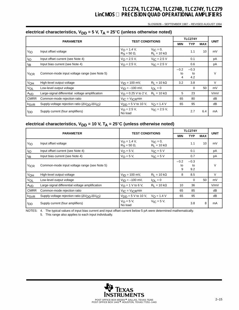
electrical characteristics, V DD = 5 V, TA = 25°C (unless otherwise noted)
PARAMETER TEST CONDITIONSTLC274Y
UNITPARAMETER TEST CONDITIONSMIN TYP MAX
UNIT
VIO Input offset voltageVO = 1.4 V,RS = 50 Ω,
VIC = 0,RL = 10 kΩ 1.1 10 mV
IIO Input offset current (see Note 4) VO = 2.5 V, VIC = 2.5 V 0.1 pA
IIB Input bias current (see Note 4) VO = 2.5 V, VIC = 2.5 V 0.6 pA
VICR Common-mode input voltage range (see Note 5)–0.2
to4
–0.3to
4.2V
VOH High-level output voltage VID = 100 mV, RL = 10 kΩ 3.2 3.8 V
VOL Low-level output voltage VID = –100 mV, IOL = 0 0 50 mV
AVD Large-signal differential voltage amplification VO = 0.25 V to 2 V, RL = 10 kΩ 5 23 V/mV
CMRR Common-mode rejection ratio VIC = VICRmin 65 80 dB
kSVR Supply-voltage rejection ratio (∆VDD/∆VIO) VDD = 5 V to 10 V, VO = 1.4 V 65 95 dB
IDD Supply current (four amplifiers)VO = 2.5 V,No load
VIC = 2.5 V,2.7 6.4 mA
electrical characteristics, V DD = 10 V, TA = 25°C (unless otherwise noted)
PARAMETER TEST CONDITIONSTLC274Y
UNITPARAMETER TEST CONDITIONSMIN TYP MAX
UNIT
VIO Input offset voltageVO = 1.4 V,RS = 50 Ω,
VIC = 0,RL = 10 kΩ 1.1 10 mV
IIO Input offset current (see Note 4) VO = 5 V, VIC = 5 V 0.1 pA
IIB Input bias current (see Note 4) VO = 5 V, VIC = 5 V 0.7 pA
VICR Common-mode input voltage range (see Note 5)–0.2
to9
–0.3to
9.2V
VOH High-level output voltage VID = 100 mV, RL = 10 kΩ 8 8.5 V
VOL Low-level output voltage VID = –100 mV, IOL = 0 0 50 mV
AVD Large-signal differential voltage amplification VO = 1 V to 6 V, RL = 10 kΩ 10 36 V/mV
CMRR Common-mode rejection ratio VIC = VICRmin 65 85 dB
kSVR Supply-voltage rejection ratio (∆VDD/∆VIO) VDD = 5 V to 10 V, VO = 1.4 V 65 95 dB
IDD Supply current (four amplifiers)VO = 5 V,No load
VIC = 5 V,3.8 8 mA
NOTES: 4. The typical values of input bias current and input offset current below 5 pA were determined mathematically.5. This range also applies to each input individually.

TLC274, TLC274A, TLC274B, TLC274Y, TLC279LinCMOS PRECISION QUAD OPERATIONAL AMPLIFIERS
SLOS092B – SEPTEMBER 1987 – REVISED AUGUST 1994
2–16 POST OFFICE BOX 655303 • DALLAS, TEXAS 75265POST OFFICE BOX 1443 • HOUSTON, TEXAS 77251–1443
operating characteristics, V DD = 5 V, TA = 25°C
PARAMETER TEST CONDITIONSTLC274Y
UNITPARAMETER TEST CONDITIONSMIN TYP MAX
UNIT
SR Slew rate at unity gainRL = 10 kΩ, CL = 20 PF, VIPP = 1 V 3.6
V/µsSR Slew rate at unity gainRL 10 kΩ,See Figure 1
CL 20 PF,
VIPP = 2.5 V 2.9V/µs
Vn Equivalent input noise voltage f = 1 kHz, RS = 20 Ω, See Figure 2 25 nV/√Hz
BOM Maximum output-swing bandwidthVO = VOH,See Figure 1
CL = 20 PF, RL = 10 kΩ,320 kHz
B1 Unity-gain bandwidth VI = 10 mV, CL = 20 PF, See Figure 3 1.7 MHz
φm Phase marginVI = 10 mV, See Figure 3
f = B1, CL = 20 PF,46°
operating characteristics, V DD = 10 V, TA = 25°C
PARAMETER TEST CONDITIONSTLC274Y
UNITPARAMETER TEST CONDITIONSMIN TYP MAX
UNIT
SR Slew rate at unity gainRL = 10 kΩ, CL = 20 PF, VIPP = 1 V 5.3
V/µsSR Slew rate at unity gainRL 10 kΩ,See Figure 1
CL 20 PF,
VIPP = 5.5 V 4.6V/µs
Vn Equivalent input noise voltage f = 1 kHz, RS = 20 Ω, See Figure 2 25 nV/√Hz
BOM Maximum output-swing bandwidthVO = VOH,See Figure 1
CL = 20 PF, RL = 10 kΩ,200 kHz
B1 Unity-gain bandwidth VI = 10 mV, CL = 20 PF, See Figure 3 2.2 MHz
φm Phase marginVI = 10 mV, See Figure 3
f = B1, CL = 20 PF,49°

TLC274, TLC274A, TLC274B, TLC274Y, TLC279 LinCMOS PRECISION QUAD OPERATIONAL AMPLIFIERS
SLOS092B – SEPTEMBER 1987 – REVISED AUGUST 1994
2–17POST OFFICE BOX 655303 • DALLAS, TEXAS 75265POST OFFICE BOX 1443 • HOUSTON, TEXAS 77251–1443
PARAMETER MEASUREMENT INFORMATION
single-supply versus split-supply test circuits
Because the TLC274 and TLC279 are optimized for single-supply operation, circuit configurations used for thevarious tests often present some inconvenience since the input signal, in many cases, must be offset fromground. This inconvenience can be avoided by testing the device with split supplies and the output load tied tothe negative rail. A comparison of single-supply versus split-supply test circuits is shown below. The use of eithercircuit gives the same result.
–
+
VDD
CL RLVI VI RLCL
–
+
VDD+
VDD–
(a) SINGLE SUPPLY (b) SPLIT SUPPLY
VOVO
Figure 1. Unity-Gain Amplifier
VDD
–
+VDD+
–
+
1/2 VDD
20 Ω
VO
2 kΩ
20 Ω
VDD–
20 Ω 20 Ω
2 kΩ
VO
(b) SPLIT SUPPLY(a) SINGLE SUPPLY
Figure 2. Noise-Test Circuit
VDD
–
+
10 kΩ
100 Ω
CL
1/2 VDD
VI VI
CL
100 Ω
10 kΩ
–
+
VDD+
VDD–
(b) SPLIT SUPPLY(a) SINGLE SUPPLY
VO VO
Figure 3. Gain-of-100 Inverting Amplifier

TLC274, TLC274A, TLC274B, TLC274Y, TLC279LinCMOS PRECISION QUAD OPERATIONAL AMPLIFIERS
SLOS092B – SEPTEMBER 1987 – REVISED AUGUST 1994
2–18 POST OFFICE BOX 655303 • DALLAS, TEXAS 75265POST OFFICE BOX 1443 • HOUSTON, TEXAS 77251–1443
PARAMETER MEASUREMENT INFORMATION
input bias current
Because of the high input impedance of the TLC274 and TLC279 operational amplifiers, attempts to measurethe input bias current can result in erroneous readings. The bias current at normal room ambient temperatureis typically less than 1 pA, a value that is easily exceeded by leakages on the test socket. Two suggestions areoffered to avoid erroneous measurements:
1. Isolate the device from other potential leakage sources. Use a grounded shield around and between thedevice inputs (see Figure 4). Leakages that would otherwise flow to the inputs are shunted away.
2. Compensate for the leakage of the test socket by actually performing an input bias current test (usinga picoammeter) with no device in the test socket. The actual input bias current can then be calculatedby subtracting the open-socket leakage readings from the readings obtained with a device in the testsocket.
One word of caution: many automatic testers as well as some bench-top operational amplifier testers use theservo-loop technique with a resistor in series with the device input to measure the input bias current (the voltagedrop across the series resistor is measured and the bias current is calculated). This method requires that adevice be inserted into the test socket to obtain a correct reading; therefore, an open-socket reading is notfeasible using this method.
V = VIC
148
17
Figure 4. Isolation Metal Around Device Inputs (J and N packages)
low-level output voltage
To obtain low-supply-voltage operation, some compromise was necessary in the input stage. This compromiseresults in the device low-level output being dependent on both the common-mode input voltage level as wellas the differential input voltage level. When attempting to correlate low-level output readings with those quotedin the electrical specifications, these two conditions should be observed. If conditions other than these are tobe used, please refer to Figures 14 through 19 in the Typical Characteristics of this data sheet.
input offset voltage temperature coefficient
Erroneous readings often result from attempts to measure temperature coefficient of input offset voltage. Thisparameter is actually a calculation using input offset voltage measurements obtained at two differenttemperatures. When one (or both) of the temperatures is below freezing, moisture can collect on both the deviceand the test socket. This moisture results in leakage and contact resistance, which can cause erroneous inputoffset voltage readings. The isolation techniques previously mentioned have no effect on the leakage since themoisture also covers the isolation metal itself, thereby rendering it useless. It is suggested that thesemeasurements be performed at temperatures above freezing to minimize error.

TLC274, TLC274A, TLC274B, TLC274Y, TLC279 LinCMOS PRECISION QUAD OPERATIONAL AMPLIFIERS
SLOS092B – SEPTEMBER 1987 – REVISED AUGUST 1994
2–19POST OFFICE BOX 655303 • DALLAS, TEXAS 75265POST OFFICE BOX 1443 • HOUSTON, TEXAS 77251–1443
PARAMETER MEASUREMENT INFORMATION
full-power response
Full-power response, the frequency above which the operational amplifier slew rate limits the output voltageswing, is often specified two ways: full-linear response and full-peak response. The full-linear response isgenerally measured by monitoring the distortion level of the output while increasing the frequency of a sinusoidalinput signal until the maximum frequency is found above which the output contains significant distortion. Thefull-peak response is defined as the maximum output frequency, without regard to distortion, above which fullpeak-to-peak output swing cannot be maintained.
Because there is no industry-wide accepted value for significant distortion, the full-peak response is specifiedin this data sheet and is measured using the circuit of Figure 1. The initial setup involves the use of a sinusoidalinput to determine the maximum peak-to-peak output of the device (the amplitude of the sinusoidal wave isincreased until clipping occurs). The sinusoidal wave is then replaced with a square wave of the same amplitude.The frequency is then increased until the maximum peak-to-peak output can no longer be maintained (Figure 5).A square wave is used to allow a more accurate determination of the point at which the maximum peak-to-peakoutput is reached.
(a) f = 1 kHz (b) BOM > f > 1 kHz (c) f = BOM (d) f > BOM
Figure 5. Full-Power-Response Output Signal
test time
Inadequate test time is a frequent problem, especially when testing CMOS devices in a high-volume,short-test-time environment. Internal capacitances are inherently higher in CMOS than in bipolar and BiFETdevices and require longer test times than their bipolar and BiFET counterparts. The problem becomes morepronounced with reduced supply levels and lower temperatures.
TLC274, TLC274A, TLC274B, TLC274Y, TLC279LinCMOS PRECISION QUAD OPERATIONAL AMPLIFIERS
SLOS092B – SEPTEMBER 1987 – REVISED AUGUST 1994
2–20 POST OFFICE BOX 655303 • DALLAS, TEXAS 75265POST OFFICE BOX 1443 • HOUSTON, TEXAS 77251–1443
TYPICAL CHARACTERISTICS
Table of Graphs
FIGURE
VIO Input offset voltage Distribution 6, 7
αVIO Temperature coefficient of input offset voltage Distribution 8, 9
V Hi h l l lvs High-level output current 10, 11
VOH High-level output voltagevs High level output currentvs Supply voltage
10, 1112OH g p g pp y g
vs Free-air temperature 13
V L l l l
vs Common-mode input voltage 14, 15
VOL Low-level output voltage
vs Common-mode input voltagevs Differential input voltage
14, 1516VOL Low-level output voltage vs Differential input voltage
vs Free-air temperature1617p
vs Low-level output current 18, 19
A L i l diff i l l lifi ivs Supply voltage 20
AVD Large-signal differential voltage amplificationvs Supply voltagevs Free-air temperature
2021VD g g g p p
vs Frequency 32, 33
IIB Input bias current vs Free-air temperature 22
IIO Input offset current vs Free-air temperature 22
VIC Common-mode input voltage vs Supply voltage 23
IDD Supply currentvs Supply voltage 24
IDD Supply currentvs Supply voltagevs Free-air temperature
2425
SR Slew ratevs Supply voltage 26
SR Slew ratevs Supply voltagevs Free-air temperature
2627
Normalized slew rate vs Free-air temperature 28
VO(PP) Maximum peak-to-peak output voltage vs Frequency 29
B1 Unity-gain bandwidthvs Free-air temperature 30
B1 Unity-gain bandwidthvs Free air temperaturevs Supply voltage
3031
Ph ivs Supply voltage 34
φm Phase marginvs Supply voltagevs Free-air temperature
3435φm g p
vs Load capacitance 36
Vn Equivalent input noise voltage vs Frequency 37
Phase shift vs Frequency 32, 33

TLC274, TLC274A, TLC274B, TLC274Y, TLC279 LinCMOS PRECISION QUAD OPERATIONAL AMPLIFIERS
SLOS092B – SEPTEMBER 1987 – REVISED AUGUST 1994
2–21POST OFFICE BOX 655303 • DALLAS, TEXAS 75265POST OFFICE BOX 1443 • HOUSTON, TEXAS 77251–1443
TYPICAL CHARACTERISTICS
50
40
30
20
10
43210–1–2–3–4
60
5VIO – Input Offset Voltage – mV
Per
cent
age
of U
nits
– %
0–5
N PackageTA = 25°CVDD = 10 V
–50
Per
cent
age
of U
nits
– %
VIO – Input Offset Voltage – mV5
60
–4 –3 –2 –1 0 1 2 3 4
10
20
30
40
50 TA= 25°CN Package
DISTRIBUTION OF TLC274INPUT OFFSET VOLTAGE
DISTRIBUTION OF TLC274INPUT OFFSET VOLTAGE
ÎÎÎÎÎÎÎÎÎÎÎÎÎÎÎÎÎÎÎÎÎÎÎÎ
753 Amplifiers Tested From 6 Wafer LotsVDD = 5 V
ÎÎÎÎÎÎÎÎÎÎÎÎÎÎÎÎÎÎÎÎÎÎ
753 Amplifiers Tested From 6 Wafer Lots
Figure 6 Figure 7
–100
Per
cent
age
of U
nits
– %
αVIO – Temperature Coefficient – µV/°C10
60
–8 –6 –4 –2 0 2 4 6 8
10
20
30
40
50
Outliers:
TA = 25°C to 125°CN Package
(1) 21.2 V/C
50
40
30
20
10
86420–2–4–6–8
60
10αVIO – Temperature Coefficient – µV/°C
Per
cent
age
of U
nits
– %
0–10
N PackageTA = 25°C to 125°C
ÎÎÎÎÎÎÎÎÎÎÎÎÎÎÎÎÎÎÎÎÎÎÎÎ
324 Amplifiers Tested From 8 Wafer Lots
Outliers:(1) 20.5 V/°C
DISTRIBUTION OF TLC274 AND TLC279INPUT OFFSET VOLTAGE
TEMPERATURE COEFFICIENT
DISTRIBUTION OF TLC274 AND TLC279INPUT OFFSET VOLTAGE
TEMPERATURE COEFFICIENT
VDD = 5 V
ÎÎÎÎÎÎÎÎÎÎÎÎÎÎÎÎÎÎÎÎÎÎ
324 Amplifiers Tested From 8 Wafer LotsVDD = 10 V
Figure 8 Figure 9

TLC274, TLC274A, TLC274B, TLC274Y, TLC279LinCMOS PRECISION QUAD OPERATIONAL AMPLIFIERS
SLOS092B – SEPTEMBER 1987 – REVISED AUGUST 1994
2–22 POST OFFICE BOX 655303 • DALLAS, TEXAS 75265POST OFFICE BOX 1443 • HOUSTON, TEXAS 77251–1443
TYPICAL CHARACTERISTICS †
00
– H
igh-
Leve
l Out
put V
olta
ge –
V
IOH – High-Level Output Current – mA
–10
5
–2 –4 –6 –8
1
2
3
4TA = 25°CVID = 100 mV
VDD = 5 V
VDD = 4 V
VDD = 3 V
00
IOH – High-Level Output Current – mA
–40
16
–10 –20 –30
2
4
6
8
10
12
14VDD = 16 V
VDD = 10 V
VID = 100 mVTA = 25°C
HIGH-LEVEL OUTPUT VOLTAGEvs
HIGH-LEVEL OUTPUT CURRENT
HIGH-LEVEL OUTPUT VOLTAGEvs
HIGH-LEVEL OUTPUT CURRENT
V OH
– H
igh-
Leve
l Out
put V
olta
ge –
VV O
H–35–5 –15 –25
Figure 10 Figure 11
0
VDD – Supply Voltage – V
162 4 6 8 10 12 14
14
12
10
8
6
4
2
16
0
VID = 100 mV
RL = 10 kΩTA = 25°C
HIGH-LEVEL OUTPUT VOLTAGEvs
SUPPLY VOLTAGE
HIGH-LEVEL OUTPUT VOLTAGEvs
FREE-AIR TEMPERATURE
VDD–1.7
VDD–1.8
VDD–1.9
VDD–2
VDD–2.1
VDD–2.2
VDD–2.3
1007550250–25–50
VDD–1.6
125
TA – Free-Air Temperature – °C
VDD–2.4–75
IOH = –5 mA
VID = 100 mAVDD = 5 V
VDD = 10 V
– H
igh-
Leve
l Out
put V
olta
ge –
VV O
H
– H
igh-
Leve
l Out
put V
olta
ge –
VV O
H
Figure 12 Figure 13
† Data at high and low temperatures are applicable only within the rated operating free-air temperature ranges of the various devices.

TLC274, TLC274A, TLC274B, TLC274Y, TLC279 LinCMOS PRECISION QUAD OPERATIONAL AMPLIFIERS
SLOS092B – SEPTEMBER 1987 – REVISED AUGUST 1994
2–23POST OFFICE BOX 655303 • DALLAS, TEXAS 75265POST OFFICE BOX 1443 • HOUSTON, TEXAS 77251–1443
TYPICAL CHARACTERISTICS †
2500
VIC – Common-Mode Input Voltage – V
300
350
400
450
500
2 4 6 8 10
VDD = 10 VIOL = 5 mATA = 25°C
VID = –1 V
VID = –2.5 V
VID = –100 mV
0300
– Lo
w-L
evel
Out
put V
olta
ge –
mV
VIC – Common-Mode Input Voltage – V4
700
1 2 3
400
500
600TA = 25°CIOL = 5 mAVDD = 5 V
VID = –100 mV
VID = –1 V
LOW-LEVEL OUTPUT VOLTAGEvs
COMMON-MODE INPUT VOLTAGE
LOW-LEVEL OUTPUT VOLTAGEvs
COMMON-MODE INPUT VOLTAGE
VO
L
– Lo
w-L
evel
Out
put V
olta
ge –
mV
VO
L1 3 5 7 9
650
350
450
550
Figure 14 Figure 15
LOW-LEVEL OUTPUT VOLTAGEvs
DIFFERENTIAL INPUT VOLTAGE
LOW-LEVEL OUTPUT VOLTAGEvs
FREE-AIR TEMPERATURE
0VID – Differential Input Voltage – V
–10–2 –4 –6 –8
800
700
600
500
400
300
200
100
0
VDD = 5 V
VDD = 10 V
–750
125
900
–50 –25 0 25 50 75 100
100
200
300
400
500
600
700
800
VIC = 0.5 VVID = –1 VIOL = 5 mA
VDD = 5 V
VDD = 10 V
TA – Free-Air Temperature – °C
– Lo
w-L
evel
Out
put V
olta
ge –
mV
VO
L
– Lo
w-L
evel
Out
put V
olta
ge –
mV
VO
L
IOL = 5 mAVIC = |VID/2|TA = 25°C
–9–1 –3 –5 –7
Figure 16 Figure 17
† Data at high and low temperatures are applicable only within the rated operating free-air temperature ranges of the various devices.

TLC274, TLC274A, TLC274B, TLC274Y, TLC279LinCMOS PRECISION QUAD OPERATIONAL AMPLIFIERS
SLOS092B – SEPTEMBER 1987 – REVISED AUGUST 1994
2–24 POST OFFICE BOX 655303 • DALLAS, TEXAS 75265POST OFFICE BOX 1443 • HOUSTON, TEXAS 77251–1443
TYPICAL CHARACTERISTICS †
0IOL – Low-Level Output Current – mA
3
300
5 10 15 20 25
0.5
1
1.5
2
2.5 TA = 25°CVIC = 0.5 VVID = –1 V
VDD = 10 V
ÎÎÎÎÎÎÎÎ
VDD = 16 V
0IOL – Low-Level Output Current – mA
1
80
1 2 3 4 5 6 7
0.1
0.2
0.3
0.4
0.5
0.6
0.7
0.8
0.9VID = –1 VVIC = 0.5 VTA = 25°C
VDD = 3 V
VDD = 4 V
VDD = 5 V
LOW-LEVEL OUTPUT VOLTAGEvs
LOW-LEVEL OUTPUT CURRENT
LOW-LEVEL OUTPUT VOLTAGEvs
LOW-LEVEL OUTPUT CURRENT
– Lo
w-L
evel
Out
put V
olta
ge –
VV
OL
– Lo
w-L
evel
Out
put V
olta
ge –
VV
OL
Figure 18 Figure 19
–75
50
1250
–50 –25 0 25 50 75 100
5
10
15
20
25
30
35
40
45
VDD = 5 V
VDD = 10 V
RL = 10 kΩ
0
60
160
2 4 6 8 10 12 14
10
20
30
40
50
VDD – Supply Voltage – V
TA = –55°C
RL = 10 kΩ
LARGE-SIGNALDIFFERENTIAL VOLTAGE AMPLIFICATION
vsSUPPLY VOLTAGE
LARGE-SIGNALDIFFERENTIAL VOLTAGE AMPLIFICATION
vsFREE-AIR TEMPERATURE
TA – Free-Air Temperature – °C
ÎÎÎÎÎÎ
TA = 25°CÎÎÎÎÎÎ
TA = 85°C
ÎÎÎÎTA = 125°C
ÎÎÎÎTA = 0°C
AV
D –
Lar
ge-S
igna
l Diff
eren
tial
ÁÁÁÁ
AV
DVo
ltage
Am
plifi
catio
n –
V/m
V
AV
D –
Lar
ge-S
igna
l Diff
eren
tial
ÁÁÁÁ
AV
DVo
ltage
Am
plifi
catio
n –
V/m
V
Figure 20 Figure 21
† Data at high and low temperatures are applicable only within the rated operating free-air temperature ranges of the various devices.

TLC274, TLC274A, TLC274B, TLC274Y, TLC279 LinCMOS PRECISION QUAD OPERATIONAL AMPLIFIERS
SLOS092B – SEPTEMBER 1987 – REVISED AUGUST 1994
2–25POST OFFICE BOX 655303 • DALLAS, TEXAS 75265POST OFFICE BOX 1443 • HOUSTON, TEXAS 77251–1443
TYPICAL CHARACTERISTICS †
INPUT BIAS CURRENT AND INPUT OFFSET CURRENTvs
FREE-AIR TEMPERATURE
COMMON-MODEINPUT VOLTAGE POSITIVE LIMIT
vsSUPPLY VOLTAGE
0VDD – Supply Voltage – V
16
160
2 4 6 8 10 12 14
2
4
6
8
10
12
14TA = 25°C
0.1125
10000
45 65 85 105
1
10
100
1000
25
– In
put B
ias
and
Offs
et C
urre
nts
– pA
VDD = 10 VVIC = 5 VSee Note A
ÎÎÎÎ
IIB
I IB
ICV
I IO
and
– C
omm
on-M
ode
Inpu
t Vol
tage
– V
TA – Free-Air Temperature – °C
ÎÎIIO
NOTE A: The typical values of input bias current and input offsetcurrent below 5 pA were determined mathematically.
Figure 22 Figure 23
SUPPLY CURRENTvs
SUPPLY VOLTAGE
SUPPLY CURRENTvs
FREE-AIR TEMPERATURE
0VDD – Supply Voltage – V
10
160
2 4 6 8 10 12 14
2
4
6
8
VO = VDD/2No Load
TA = –55°C
–75
– S
uppl
y C
urre
nt –
mA
4
1250
1
2
3
–50 –25 0 25 50 75 100
No LoadVO = VDD/2
VDD = 10 V
VDD = 5 V
5
6
7
8
I DD
TA – Free-Air Temperature – °C
– S
uppl
y C
urre
nt –
mA
I DD
1
3
5
7
9
ÎÎÎÎÎÎÎÎ
TA = 70°C
ÎÎÎÎTA = 125°C
ÎÎÎÎÎÎÎÎ
TA = 0°CÎÎÎÎÎÎTA = 25°C
Figure 24 Figure 25
† Data at high and low temperatures are applicable only within the rated operating free-air temperature ranges of the various devices.

TLC274, TLC274A, TLC274B, TLC274Y, TLC279LinCMOS PRECISION QUAD OPERATIONAL AMPLIFIERS
SLOS092B – SEPTEMBER 1987 – REVISED AUGUST 1994
2–26 POST OFFICE BOX 655303 • DALLAS, TEXAS 75265POST OFFICE BOX 1443 • HOUSTON, TEXAS 77251–1443
TYPICAL CHARACTERISTICS †
TA – Free-Air Temperature – °C125–50 –25 0 25 50 75 100
8
7
6
5
4
3
2
1
0–75
CL = 20 pFSee Figure 1
AV = 1RL = 10 k Ω
ÎÎÎÎÎÎÎÎÎÎ
VDD = 10 V
VDD = 5 VVIPP = 1 V
VDD = 5 VVIPP = 2.5 V
VDD = 10 VVIPP = 1 V
0VDD – Supply Voltage – V
160
2 4 6 8 10 12 14
1
2
3
4
5
6
7
8
CL = 20 pFRL = 10 k ΩVIPP = 1 VAV = 1
See Figure 1TA = 25°C
SLEW RATEvs
SUPPLY VOLTAGE
SLEW RATEvs
FREE-AIR TEMPERATURE
ÎÎÎÎÎÎÎÎÎÎ
VIPP = 5.5 V
µsS
R –
Sle
w R
ate
– V
/ µsS
R –
Sle
w R
ate
– V
/
Figure 26 Figure 27
–75
Nor
mal
ized
Sle
w R
ate
TA – Free-Air Temperature – °C125–50 –25 0 25 50 75 100
AV = 1VIPP = 1 VRL = 10 kΩCL = 20 pF
1.4
1.3
1.2
1.1
1
0.9
0.8
0.7
0.6
0.5
1.5
VDD = 10 V
VDD = 5 V
10f – Frequency – kHz
10
100000
1
2
3
4
5
6
7
8
9
100 1000
VDD = 10 V
VDD = 5 V
See Figure 1RL = 10 k Ω
TA = 125°CTA = 25°CTA = –55°C
NORMALIZED SLEW RATEvs
FREE-AIR TEMPERATURE
MAXIMUM PEAK-TO-PEAK OUTPUT VOLTAGEvs
FREQUENCY
– M
axim
um P
eak-
to-P
eak
Out
put V
olta
ge –
VV O
(PP
)
Figure 28 Figure 29
† Data at high and low temperatures are applicable only within the rated operating free-air temperature ranges of the various devices.

TLC274, TLC274A, TLC274B, TLC274Y, TLC279 LinCMOS PRECISION QUAD OPERATIONAL AMPLIFIERS
SLOS092B – SEPTEMBER 1987 – REVISED AUGUST 1994
2–27POST OFFICE BOX 655303 • DALLAS, TEXAS 75265POST OFFICE BOX 1443 • HOUSTON, TEXAS 77251–1443
TYPICAL CHARACTERISTICS †
VDD = 5 VVI = 10 mV
CL = 20 pFSee Figure 3
–75TA – Free-Air Temperature – °C
3
1251
–50 –25 0 25 50 75 100
1.5
2
2.5 See Figure 3TA = 25°CCL = 20 pFVI = 10 mV
0VDD – Supply Voltage – V
2.5
161
2 4 6 8 10 12 14
1.5
2
UNITY-GAIN BANDWIDTHvs
FREE-AIR TEMPERATURE
UNITY-GAIN BANDWIDTHvs
SUPPLY VOLTAGE
– U
nity
-Gai
n B
andw
idth
– M
Hz
B1
– U
nity
-Gai
n B
andw
idth
– M
Hz
B1
Figure 30 Figure 31
10f – Frequency – Hz
10 M0.1
100 1 k 10 k 100 k 1 M
1
10
102
103
104
105
106
150°
120°
90°
60°
30°
0°
180°
TA = 25°CRL = 10 k ΩVDD = 5 V
AVD
Phase Shift
107
LARGE-SIGNAL DIFFERENTIAL VOLTAGEAMPLIFICATION AND PHASE SHIFT
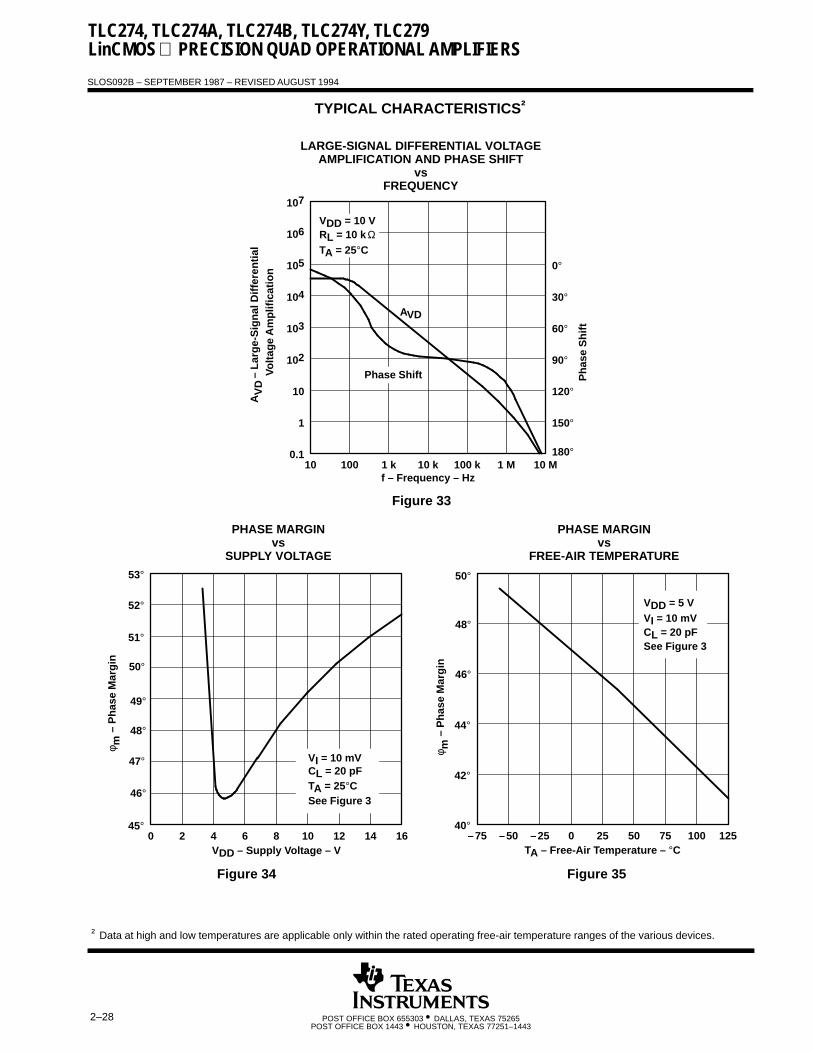
vsFREQUENCY
Pha
se S
hift
AV
D –
Lar
ge-S
igna
l Diff
eren
tial
ÁÁÁÁÁÁ
AV
DVo
ltage
Am
plifi
catio
n
Figure 32
† Data at high and low temperatures are applicable only within the rated operating free-air temperature ranges of the various devices.
TLC274, TLC274A, TLC274B, TLC274Y, TLC279LinCMOS PRECISION QUAD OPERATIONAL AMPLIFIERS
SLOS092B – SEPTEMBER 1987 – REVISED AUGUST 1994
2–28 POST OFFICE BOX 655303 • DALLAS, TEXAS 75265POST OFFICE BOX 1443 • HOUSTON, TEXAS 77251–1443
TYPICAL CHARACTERISTICS †
10f – Frequency – Hz
10 M0.1
100 1 k 10 k 100 k 1 M
1
10
102
103
104
105
106
180°
0°
30°
60°
90°
120°
150°
VDD = 10 VRL = 10 k ΩTA = 25°C
AVD
Phase Shift
107
LARGE-SIGNAL DIFFERENTIAL VOLTAGEAMPLIFICATION AND PHASE SHIFT
vsFREQUENCY
Pha
se S
hift
AV
D –
Lar
ge-S
igna
l Diff
eren
tial
ÁÁÁ
AV
DVo
ltage
Am
plifi
catio
n
Figure 33
0
– P
hase
Mar
gin
VDD – Supply Voltage – V
53°
162 4 6 8 10 12 14
51°
CL = 20 pFTA = 25°C
VI = 10 mV
See Figure 3
45°–75 125
40°–50 –25 0 25 50 75 100
42°
44°
VDD = 5 V
CL = 20 pFVI = 10 mV
See Figure 3
TA – Free-Air Temperature – °C
PHASE MARGINvs
SUPPLY VOLTAGE
PHASE MARGINvs
FREE-AIR TEMPERATURE
φ m
– P
hase
Mar
gin
φ m
52°
50°
49°
48°
47°
46°
50°
46°
48°
Figure 34 Figure 35
† Data at high and low temperatures are applicable only within the rated operating free-air temperature ranges of the various devices.

TLC274, TLC274A, TLC274B, TLC274Y, TLC279 LinCMOS PRECISION QUAD OPERATIONAL AMPLIFIERS
SLOS092B – SEPTEMBER 1987 – REVISED AUGUST 1994
2–29POST OFFICE BOX 655303 • DALLAS, TEXAS 75265POST OFFICE BOX 1443 • HOUSTON, TEXAS 77251–1443
TYPICAL CHARACTERISTICS
0CL – Capacitive Load – pF
10025°
20 40 60 80
30°
35°
See Figure 3
VI = 10 mVTA = 25°C
VDD = 5 V
1
– E
quiv
alen
t Inp
ut N
oise
Vol
tage
–
f – Frequency – Hz
400
10000
100
200
300
10 100
VDD = 5 V
TA = 25°CRS = 20 Ω
See Figure 2
PHASE MARGINvs
CAPACITIVE LOAD
EQUIVALENT INPUT NOISE VOLTAGEvs
FREQUENCY
nV/
Hz
– P
hase
Mar
gin
φ m
Vn
45°
50°
40°
10 30 50 70 90
Figure 36 Figure 37

TLC274, TLC274A, TLC274B, TLC274Y, TLC279LinCMOS PRECISION QUAD OPERATIONAL AMPLIFIERS
SLOS092B – SEPTEMBER 1987 – REVISED AUGUST 1994
2–30 POST OFFICE BOX 655303 • DALLAS, TEXAS 75265POST OFFICE BOX 1443 • HOUSTON, TEXAS 77251–1443
APPLICATION INFORMATION
single-supply operation
While the TLC274 and TLC279 perform well using dual power supplies (also called balanced or split supplies),the design is optimized for single-supply operation. This design includes an input common-mode voltage rangethat encompasses ground as well as an output voltage range that pulls down to ground. The supply voltagerange extends down to 3 V (C-suffix types), thus allowing operation with supply levels commonly available forTTL and HCMOS; however, for maximum dynamic range, 16-V single-supply operation is recommended.
Many single-supply applications require that a voltage be applied to one input to establish a reference level thatis above ground. A resistive voltage divider is usually sufficient to establish this reference level (see Figure 38).The low input bias current of the TLC274 and TLC279 permits the use of very large resistive values to implementthe voltage divider, thus minimizing power consumption.
The TLC274 and TLC279 work well in conjunction with digital logic; however, when powering both linear devicesand digital logic from the same power supply, the following precautions are recommended:
1. Power the linear devices from separate bypassed supply lines (see Figure 39); otherwise the lineardevice supply rails can fluctuate due to voltage drops caused by high switching currents in the digitallogic.
2. Use proper bypass techniques to reduce the probability of noise-induced errors. Single capacitivedecoupling is often adequate; however, high-frequency applications may require RC decoupling.
R4
VO
VDD
R2R1
VI
VREFR3 C
0.01 µF
–
+
VREF = VDDR3
R1 + R3
VO = (VREF – VI )R4R2
+ VREF
Figure 38. Inverting Amplifier With Voltage Reference
LogicLogicLogic
–
+
–
+
(a) COMMON SUPPLY RAILS
(b) SEPARATE BYPASSED SUPPLY RAILS (preferred)
Logic Logic LogicPowerSupply
PowerSupply
VO
VO
Figure 39. Common Versus Separate Supply Rails

TLC274, TLC274A, TLC274B, TLC274Y, TLC279 LinCMOS PRECISION QUAD OPERATIONAL AMPLIFIERS
SLOS092B – SEPTEMBER 1987 – REVISED AUGUST 1994
2–31POST OFFICE BOX 655303 • DALLAS, TEXAS 75265POST OFFICE BOX 1443 • HOUSTON, TEXAS 77251–1443
APPLICATION INFORMATION
input characteristics
The TLC274 and TLC279 are specified with a minimum and a maximum input voltage that, if exceeded at eitherinput, could cause the device to malfunction. Exceeding this specified range is a common problem, especiallyin single-supply operation. Note that the lower range limit includes the negative rail, while the upper range limitis specified at VDD – 1 V at TA = 25°C and at VDD – 1.5 V at all other temperatures.
The use of the polysilicon-gate process and the careful input circuit design gives the TLC274 and TLC279 verygood input offset voltage drift characteristics relative to conventional metal-gate processes. Offset voltage driftin CMOS devices is highly influenced by threshold voltage shifts caused by polarization of the phosphorusdopant implanted in the oxide. Placing the phosphorus dopant in a conductor (such as a polysilicon gate)alleviates the polarization problem, thus reducing threshold voltage shifts by more than an order of magnitude.The offset voltage drift with time has been calculated to be typically 0.1 µV/month, including the first month ofoperation.
Because of the extremely high input impedance and resulting low bias current requirements, the TLC274 andTLC279 are well suited for low-level signal processing; however, leakage currents on printed-circuit boards andsockets can easily exceed bias current requirements and cause a degradation in device performance. It is goodpractice to include guard rings around inputs (similar to those of Figure 4 in the Parameter MeasurementInformation section). These guards should be driven from a low-impedance source at the same voltage levelas the common-mode input (see Figure 40).
Unused amplifiers should be connected as grounded unity-gain followers to avoid possible oscillation.
noise performance
The noise specifications in operational amplifier circuits are greatly dependent on the current in the first-stagedifferential amplifier. The low input bias current requirements of the TLC274 and TLC279 result in a very lownoise current, which is insignificant in most applications. This feature makes the devices especially favorableover bipolar devices when using values of circuit impedance greater than 50 kΩ, since bipolar devices exhibitgreater noise currents.
VI
(a) NONINVERTING AMPLIFIER (c) UNITY-GAIN AMPLIFIER
–
+
(b) INVERTING AMPLIFIER
VI
–
+
–
+VIVO VO VO
Figure 40. Guard-Ring Schemes
output characteristics
The output stage of the TLC274 and TLC279 is designed to sink and source relatively high amounts of current(see typical characteristics). If the output is subjected to a short-circuit condition, this high current capability cancause device damage under certain conditions. Output current capability increases with supply voltage.
All operating characteristics of the TLC274 and TLC279 were measured using a 20-pF load. The devices drivehigher capacitive loads; however, as output load capacitance increases, the resulting response pole occurs atlower frequencies, thereby causing ringing, peaking, or even oscillation (see Figure 41). In many cases, addinga small amount of resistance in series with the load capacitance alleviates the problem.

TLC274, TLC274A, TLC274B, TLC274Y, TLC279LinCMOS PRECISION QUAD OPERATIONAL AMPLIFIERS
SLOS092B – SEPTEMBER 1987 – REVISED AUGUST 1994
2–32 POST OFFICE BOX 655303 • DALLAS, TEXAS 75265POST OFFICE BOX 1443 • HOUSTON, TEXAS 77251–1443
APPLICATION INFORMATION
output characteristics (continued)
–
+
2.5 V
VO
CL
–2.5 V
VI
(d) TEST CIRCUIT
TA = 25°Cf = 1 kHzVIPP = 1 V
(a) CL = 20 pF, RL = NO LOAD (b) C L = 130 pF, RL = NO LOAD
(c) CL = 150 pF, RL = NO LOAD
Figure 41. Effect of Capacitive Loads and Test Circuit
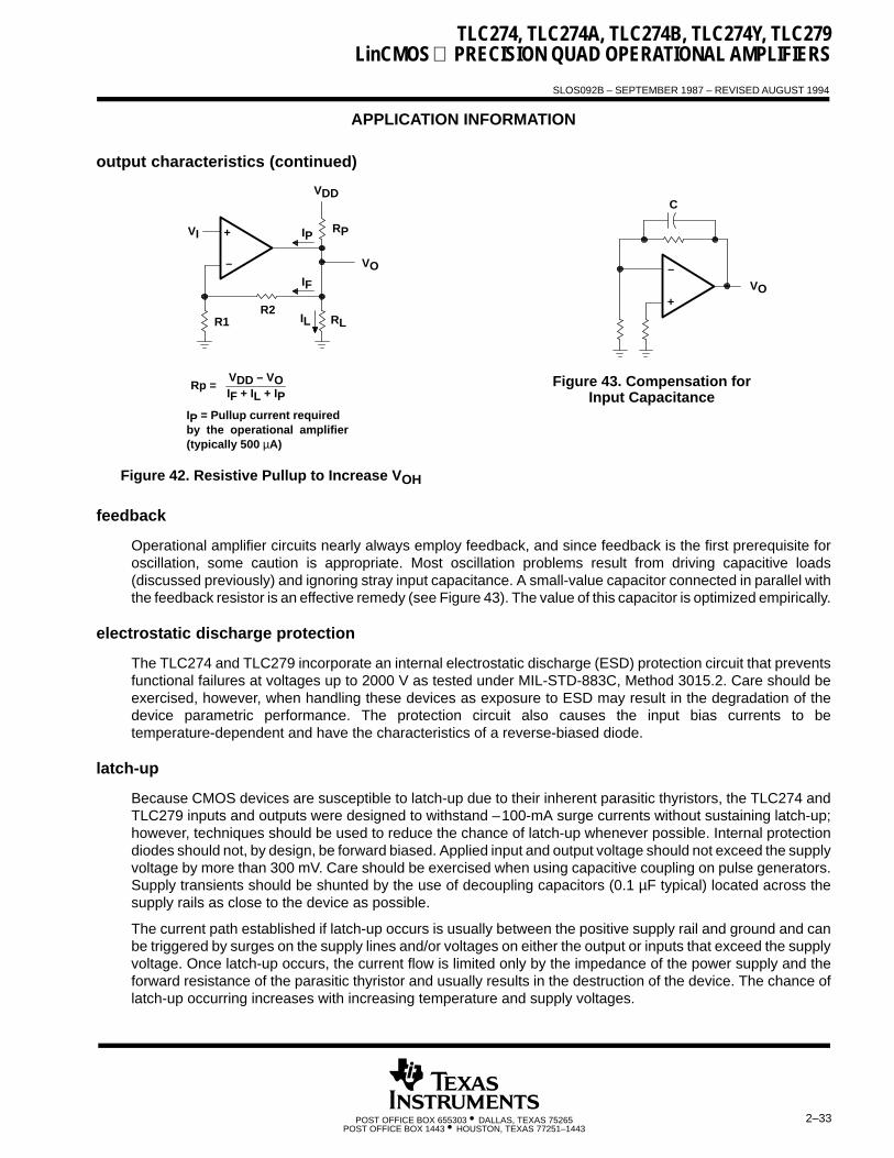
Although the TLC274 and TLC279 possess excellent high-level output voltage and current capability, methodsfor boosting this capability are available, if needed. The simplest method involves the use of a pullup resistor(RP) connected from the output to the positive supply rail (see Figure 42). There are two disadvantages to theuse of this circuit. First, the NMOS pulldown transistor N4 (see equivalent schematic) must sink a comparativelylarge amount of current. In this circuit, N4 behaves like a linear resistor with an on-resistance betweenapproximately 60 Ω and 180 Ω, depending on how hard the op amp input is driven. With very low values of RP,a voltage offset from 0 V at the output occurs. Second, pullup resistor RP acts as a drain load to N4 and the gainof the operational amplifier is reduced at output voltage levels where N5 is not supplying the output current.
TLC274, TLC274A, TLC274B, TLC274Y, TLC279 LinCMOS PRECISION QUAD OPERATIONAL AMPLIFIERS
SLOS092B – SEPTEMBER 1987 – REVISED AUGUST 1994
2–33POST OFFICE BOX 655303 • DALLAS, TEXAS 75265POST OFFICE BOX 1443 • HOUSTON, TEXAS 77251–1443
APPLICATION INFORMATION
output characteristics (continued)
–
+VI
VDD
RP
VO
R2R1 RL
IP
IF
IL
–
+
C
IP = Pullup current required by the operational amplifier(typically 500 µA)
VO
Rp =VDD – VOIF + IL + IP
Figure 42. Resistive Pullup to Increase V OH
Figure 43. Compensation forInput Capacitance
feedback
Operational amplifier circuits nearly always employ feedback, and since feedback is the first prerequisite foroscillation, some caution is appropriate. Most oscillation problems result from driving capacitive loads(discussed previously) and ignoring stray input capacitance. A small-value capacitor connected in parallel withthe feedback resistor is an effective remedy (see Figure 43). The value of this capacitor is optimized empirically.
electrostatic discharge protection
The TLC274 and TLC279 incorporate an internal electrostatic discharge (ESD) protection circuit that preventsfunctional failures at voltages up to 2000 V as tested under MIL-STD-883C, Method 3015.2. Care should beexercised, however, when handling these devices as exposure to ESD may result in the degradation of thedevice parametric performance. The protection circuit also causes the input bias currents to betemperature-dependent and have the characteristics of a reverse-biased diode.
latch-up
Because CMOS devices are susceptible to latch-up due to their inherent parasitic thyristors, the TLC274 andTLC279 inputs and outputs were designed to withstand –100-mA surge currents without sustaining latch-up;however, techniques should be used to reduce the chance of latch-up whenever possible. Internal protectiondiodes should not, by design, be forward biased. Applied input and output voltage should not exceed the supplyvoltage by more than 300 mV. Care should be exercised when using capacitive coupling on pulse generators.Supply transients should be shunted by the use of decoupling capacitors (0.1 µF typical) located across thesupply rails as close to the device as possible.
The current path established if latch-up occurs is usually between the positive supply rail and ground and canbe triggered by surges on the supply lines and/or voltages on either the output or inputs that exceed the supplyvoltage. Once latch-up occurs, the current flow is limited only by the impedance of the power supply and theforward resistance of the parasitic thyristor and usually results in the destruction of the device. The chance oflatch-up occurring increases with increasing temperature and supply voltages.

TLC274, TLC274A, TLC274B, TLC274Y, TLC279LinCMOS PRECISION QUAD OPERATIONAL AMPLIFIERS
SLOS092B – SEPTEMBER 1987 – REVISED AUGUST 1994
2–34 POST OFFICE BOX 655303 • DALLAS, TEXAS 75265POST OFFICE BOX 1443 • HOUSTON, TEXAS 77251–1443
APPLICATION INFORMATION
5 V
0.016 µF
–
+
Low Pass
HIgh Pass
Band PassR = 5 kΩ (3/d–1)
(see Note A)
–
+
0.016 µF
10 kΩ
10 kΩ
10 kΩ –
+
VI
5 kΩ
10 kΩ
10 kΩ
1/4TLC274
TLC2741/4
1/4TLC274
NOTE A: d = damping factor, 1/Q
Figure 44. State-Variable Filter
–
+
–
+
100 kΩ
VO
N.O.Reset
0.5 µFMylar
H.P.5082-2835
12 V
VI
TLC2741/4
TLC2741/4
Figure 45. Positive-Peak Detector

TLC274, TLC274A, TLC274B, TLC274Y, TLC279 LinCMOS PRECISION QUAD OPERATIONAL AMPLIFIERS
SLOS092B – SEPTEMBER 1987 – REVISED AUGUST 1994
2–35POST OFFICE BOX 655303 • DALLAS, TEXAS 75265POST OFFICE BOX 1443 • HOUSTON, TEXAS 77251–1443
APPLICATION INFORMATION
–
+
VI(see Note A)
1.2 kΩ
4.7 kΩ
0.1 µF
22 kΩ
47 kΩ
0.01 µF
TIS193
15 Ω
0.47 µF100 kΩ
1 kΩ20 kΩTL431
TIP31
10 kΩ
250 µF,25 V
+
– VO(see Note B)
110 Ω
1/4TLC274
NOTES: A. VI = 3.5 V to 15 VB. VO = 2 V, 0 to 1 A
Figure 46. Logic-Array Power Supply–
+
R1
9 V
100 kΩ
0.1 µF
R3
10 kΩ
10 kΩ VO (see Note B)
VO (see Note A)
R2TLC274
1/4
1/4TLC274
47 kΩ
C
100 kΩ
9 V
fO = 14C(R2)
R1R2
NOTES: A. VO(PP) = 8 VB. VO(PP) = 4 V
Figure 47. Single-Supply Function Generator

TLC274, TLC274A, TLC274B, TLC274Y, TLC279LinCMOS PRECISION QUAD OPERATIONAL AMPLIFIERS
SLOS092B – SEPTEMBER 1987 – REVISED AUGUST 1994
2–36 POST OFFICE BOX 655303 • DALLAS, TEXAS 75265POST OFFICE BOX 1443 • HOUSTON, TEXAS 77251–1443
APPLICATION INFORMATION
–
+
–
+
100 kΩ10 kΩ
5 V
VI–
VI+
–5 V
–
+
10 kΩ 95 kΩ
VO
R1, 10 kΩ(see Note A)
1/4TLC279
1/4TLC279
1/4TLC279
10 kΩ
NOTE A: CMRR adjustment must be noninductive.
Figure 48. Low-Power Instrumentation Amplifier
–
+
5 V
VI
VOR10 MΩ
2C540 pF
10 MΩR
270 pFC C
270 pF
5 MΩR/2
TLC2741/4
fNOTCH 1
2RC
Figure 49. Single-Supply Twin-T Notch Filter

IMPORTANT NOTICE
Texas Instruments (TI) reserves the right to make changes to its products or to discontinue any semiconductorproduct or service without notice, and advises its customers to obtain the latest version of relevant informationto verify, before placing orders, that the information being relied on is current.
TI warrants performance of its semiconductor products and related software to the specifications applicable atthe time of sale in accordance with TI’s standard warranty. Testing and other quality control techniques areutilized to the extent TI deems necessary to support this warranty. Specific testing of all parameters of eachdevice is not necessarily performed, except those mandated by government requirements.
Certain applications using semiconductor products may involve potential risks of death, personal injury, orsevere property or environmental damage (“Critical Applications”).
TI SEMICONDUCTOR PRODUCTS ARE NOT DESIGNED, INTENDED, AUTHORIZED, OR WARRANTEDTO BE SUITABLE FOR USE IN LIFE-SUPPORT APPLICATIONS, DEVICES OR SYSTEMS OR OTHERCRITICAL APPLICATIONS.
Inclusion of TI products in such applications is understood to be fully at the risk of the customer. Use of TIproducts in such applications requires the written approval of an appropriate TI officer. Questions concerningpotential risk applications should be directed to TI through a local SC sales office.
In order to minimize risks associated with the customer’s applications, adequate design and operatingsafeguards should be provided by the customer to minimize inherent or procedural hazards.
TI assumes no liability for applications assistance, customer product design, software performance, orinfringement of patents or services described herein. Nor does TI warrant or represent that any license, eitherexpress or implied, is granted under any patent right, copyright, mask work right, or other intellectual propertyright of TI covering or relating to any combination, machine, or process in which such semiconductor productsor services might be or are used.
Copyright 1995, Texas Instruments Incorporated
![LinCMOS Programmable Low-Power Operational ......Title LinCMOS Programmable Low-Power Operational Amplifiers (Rev. D) Author Texas Instruments, Incorporated [SLOS090,D ]](https://img.pdfslide.us/doc/110x75/60c520663ed5937ead0851c0/lincmos-programmable-low-power-operational-title-lincmos-programmable-low-power.jpg)