Embed Size (px)
Citation preview
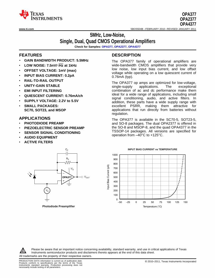
Input B
ias C
urr
ent (p
A)
-50 -25
1000
900
800
700
600
500
400
300
200
100
0
Temperature ( C)°
15050 1000 25 75 125
INPUT BIAS CURRENT vs TEMPERATURE
OPA377
CF
RF
VOUT
VB
VS
Photodiode Preamplifier
OPA377OPA2377OPA4377
www.ti.com SBOS504B –FEBRUARY 2010–REVISED JANUARY 2011
5MHz, Low-Noise,Single, Dual, Quad CMOS Operational Amplifiers
Check for Samples: OPA377, OPA2377, OPA4377
1FEATURES DESCRIPTION2• GAIN BANDWIDTH PRODUCT: 5.5MHz The OPA377 family of operational amplifiers are
wide-bandwidth CMOS amplifiers that provide very• LOW NOISE: 7.5nV/√Hz at 1kHzlow noise, low input bias current, and low offset• OFFSET VOLTAGE: 1mV (max)voltage while operating on a low quiescent current of
• INPUT BIAS CURRENT: 0.2pA 0.76mA (typ).• RAIL-TO-RAIL OUTPUT
The OPA377 op amps are optimized for low-voltage,• UNITY-GAIN STABLE single-supply applications. The exceptional
combination of ac and dc performance make them• EMI INPUT FILTERINGideal for a wide range of applications, including small• QUIESCENT CURRENT: 0.76mA/chsignal conditioning, audio, and active filters. In
• SUPPLY VOLTAGE: 2.2V to 5.5V addition, these parts have a wide supply range with• SMALL PACKAGES: excellent PSRR, making them attractive for
applications that run directly from batteries withoutSC70, SOT23, and MSOPregulation.
APPLICATIONS The OPA377 is available in the SC70-5, SOT23-5,• PHOTODIODE PREAMP and SO-8 packages. The dual OPA2377 is offered in
the SO-8 and MSOP-8, and the quad OPA4377 in the• PIEZOELECTRIC SENSOR PREAMPTSSOP-14 packages. All versions are specified for• SENSOR SIGNAL CONDITIONINGoperation from –40°C to +125°C.• AUDIO EQUIPMENT
• ACTIVE FILTERS
1
Please be aware that an important notice concerning availability, standard warranty, and use in critical applications of TexasInstruments semiconductor products and disclaimers thereto appears at the end of this data sheet.
2All trademarks are the property of their respective owners.
PRODUCTION DATA information is current as of publication date. © 2010–2011, Texas Instruments IncorporatedProducts conform to specifications per the terms of the TexasInstruments standard warranty. Production processing does notnecessarily include testing of all parameters.
OPA377OPA2377OPA4377SBOS504B –FEBRUARY 2010–REVISED JANUARY 2011 www.ti.com
This integrated circuit can be damaged by ESD. Texas Instruments recommends that all integrated circuits be handled withappropriate precautions. Failure to observe proper handling and installation procedures can cause damage.
ESD damage can range from subtle performance degradation to complete device failure. Precision integrated circuits may be moresusceptible to damage because very small parametric changes could cause the device not to meet its published specifications.
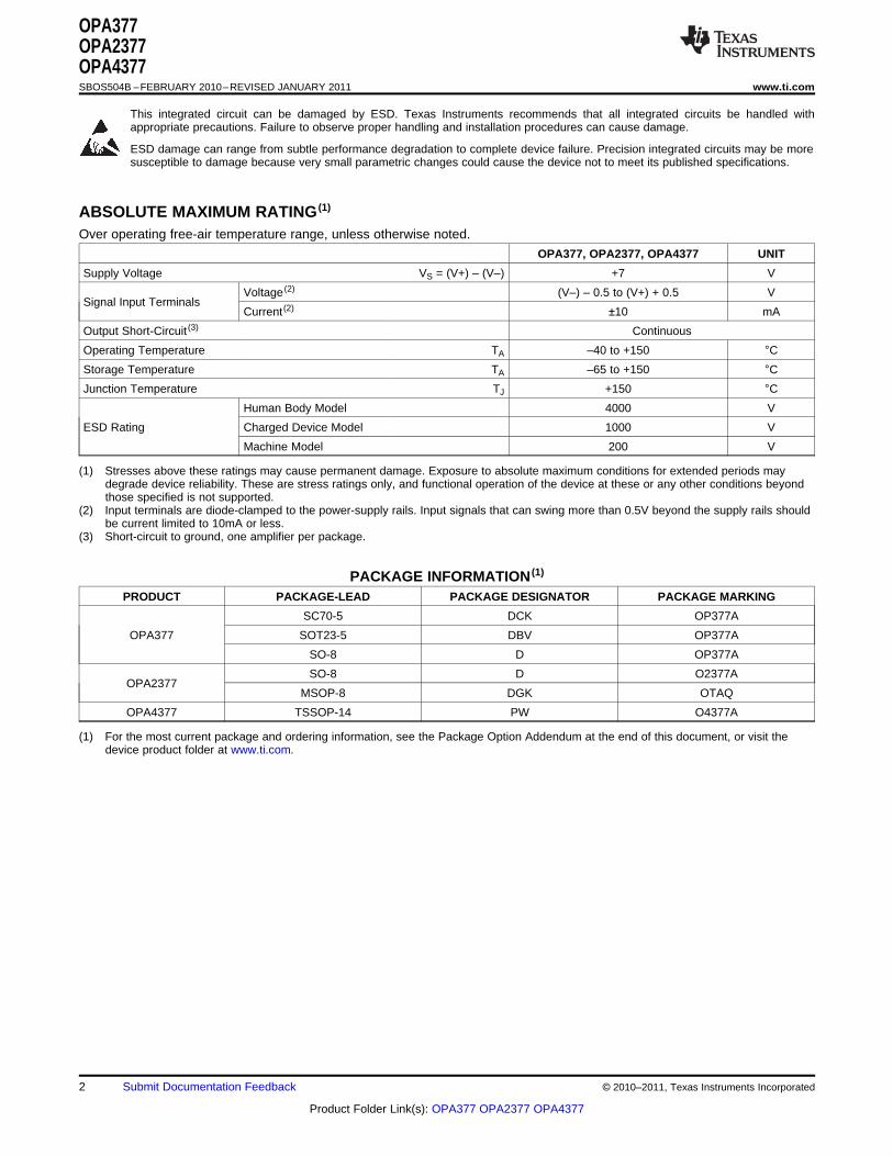
ABSOLUTE MAXIMUM RATING (1)
Over operating free-air temperature range, unless otherwise noted.
OPA377, OPA2377, OPA4377 UNIT
Supply Voltage VS = (V+) – (V–) +7 V
Voltage (2) (V–) – 0.5 to (V+) + 0.5 VSignal Input Terminals
Current (2) ±10 mA
Output Short-Circuit (3) Continuous
Operating Temperature TA –40 to +150 °CStorage Temperature TA –65 to +150 °CJunction Temperature TJ +150 °C
Human Body Model 4000 V
ESD Rating Charged Device Model 1000 V
Machine Model 200 V
(1) Stresses above these ratings may cause permanent damage. Exposure to absolute maximum conditions for extended periods maydegrade device reliability. These are stress ratings only, and functional operation of the device at these or any other conditions beyondthose specified is not supported.
(2) Input terminals are diode-clamped to the power-supply rails. Input signals that can swing more than 0.5V beyond the supply rails shouldbe current limited to 10mA or less.
(3) Short-circuit to ground, one amplifier per package.
PACKAGE INFORMATION (1)
PRODUCT PACKAGE-LEAD PACKAGE DESIGNATOR PACKAGE MARKING
SC70-5 DCK OP377A
OPA377 SOT23-5 DBV OP377A
SO-8 D OP377A
SO-8 D O2377AOPA2377
MSOP-8 DGK OTAQ
OPA4377 TSSOP-14 PW O4377A
(1) For the most current package and ordering information, see the Package Option Addendum at the end of this document, or visit thedevice product folder at www.ti.com.
2 Submit Documentation Feedback © 2010–2011, Texas Instruments Incorporated
Product Folder Link(s): OPA377 OPA2377 OPA4377
OPA377OPA2377OPA4377
www.ti.com SBOS504B –FEBRUARY 2010–REVISED JANUARY 2011
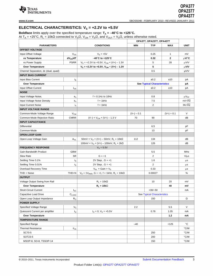
ELECTRICAL CHARACTERISTICS: VS = +2.2V to +5.5VBoldface limits apply over the specified temperature range: TA = –40°C to +125°C.At TA = +25°C, RL = 10kΩ connected to VS/2, VCM = VS/2, and VOUT = VS/2, unless otherwise noted.
OPA377, OPA2377, OPA4377
PARAMETERS CONDITIONS MIN TYP MAX UNIT
OFFSET VOLTAGE
Input Offset Voltage VOS VS = +5V 0.25 1 mV
vs Temperature dVOS/dT –40°C to +125°C 0.32 2 mV/°C
vs Power Supply PSRR VS = +2.2V to +5.5V, VCM < (V+) – 1.3V 5 28 mV/V
Over Temperature VS = +2.2V to +5.5V, VCM < (V+) – 1.3V 5 mV/V
Channel Separation, dc (dual, quad) 0.5 µV/V
INPUT BIAS CURRENT
Input Bias Current IB ±0.2 ±10 pA
Over Temperature See Typical Characteristics pA
Input Offset Current IOS ±0.2 ±10 pA
NOISE
Input Voltage Noise, en f = 0.1Hz to 10Hz 0.8 mVPP
Input Voltage Noise Density en f = 1kHz 7.5 nV/√Hz
Input Current Noise in f = 1kHz 2 fA/√Hz
INPUT VOLTAGE RANGE
Common-Mode Voltage Range VCM (V–) – 0.1 (V+) + 0.1 V
Common-Mode Rejection Ratio CMRR (V–) < VCM < (V+) – 1.3 V 70 90 dB
INPUT CAPACITANCE
Differential 6.5 pF
Common-Mode 13 pF
OPEN-LOOP GAIN
Open-Loop Voltage Gain AOL 50mV < VO < (V+) – 50mV, RL = 10kΩ 112 134 dB
100mV < VO < (V+) – 100mV, RL = 2kΩ 126 dB
FREQUENCY RESPONSE VS = 5.5V
Gain-Bandwidth Product GBW 5.5 MHz
Slew Rate SR G = +1 2 V/ms
Settling Time 0.1% tS 2V Step , G = +1 1.6 ms
Settling Time 0.01% tS 2V Step , G = +1 2 ms
Overload Recovery Time VIN × Gain > VS 0.33 ms
THD + Noise THD+N VO = 1VRMS, G = +1, f = 1kHz, RL = 10kΩ 0.00027 %
OUTPUT
Voltage Output Swing from Rail RL = 10kΩ 10 20 mV
Over Temperature RL = 10kΩ 40 mV
Short-Circuit Current ISC +30/–50 mA
Capacitive Load Drive CLOAD See Typical Characteristics
Open-Loop Output Impedance RO 150 Ω
POWER SUPPLY
Specified Voltage Range VS 2.2 5.5 V
Quiescent Current per amplifier IQ IO = 0, VS = +5.5V 0.76 1.05 mA
Over Temperature 1.2 mA
TEMPERATURE RANGE
Specified Range –40 +125 °C
Thermal Resistance qJA °C/W
SC70-5 250 °C/W
SOT23-5 200 °C/W
MSOP-8, SO-8, TSSOP-14 150 °C/W
© 2010–2011, Texas Instruments Incorporated Submit Documentation Feedback 3
Product Folder Link(s): OPA377 OPA2377 OPA4377
1
2
3
5
4
V+
-IN
OUT
V-
+IN
1
2
3
4
8
7
6
5
NC(1)
V+
OUT
NC(1)
NC(1)
-IN
+IN
V-
-
+
1
2
3
5
4
V+
OUT
+IN
V-
-IN
1
2
3
4
8
7
6
5
V+
OUT B
-IN B
+IN B
OUT A
-IN A
+IN A
V-
1
2
3
4
5
6
7
14
13
12
11
10
9
8
OUT D
-IN D
+IN D
V-
+IN C
-IN C
OUT C
OUT A
-IN A
+IN A
V+
+IN B
-IN B
OUT B
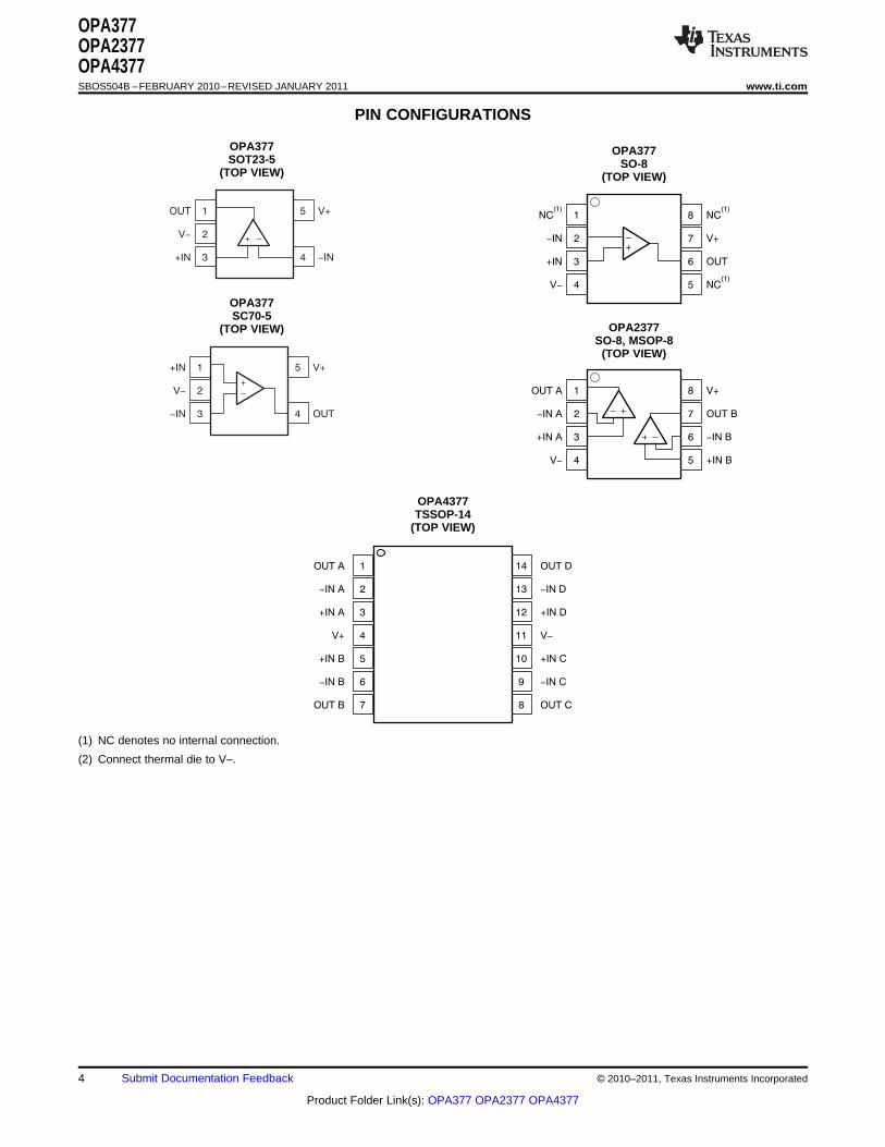
OPA377OPA2377OPA4377SBOS504B –FEBRUARY 2010–REVISED JANUARY 2011 www.ti.com
PIN CONFIGURATIONS
OPA377 OPA377SOT23-5 SO-8
(TOP VIEW) (TOP VIEW)
OPA377SC70-5
OPA2377(TOP VIEW)SO-8, MSOP-8
(TOP VIEW)
OPA4377TSSOP-14
(TOP VIEW)
(1) NC denotes no internal connection.
(2) Connect thermal die to V–.
4 Submit Documentation Feedback © 2010–2011, Texas Instruments Incorporated
Product Folder Link(s): OPA377 OPA2377 OPA4377
Pow
er-
Supply
Reje
ction R
atio (
dB
)
10
120
100
80
60
40
20
0
Frequency (Hz)
10M100k100 1k 10k 1M
V(+) Power-Supply Rejection Ratio
V( )- Power-Supply Rejection Ratio
Common-Mode
Rejection Ratio
Op
en
-Lo
op
Ga
in (
dB
)
0.1
160
140
120
100
80
60
40
20
0
-20
Ph
ase
Ma
rgin
()°
0
-20
-40
-60
-80
-100
-120
-140
-160
-180
Frequency (Hz)
10M1 100k10 100 1k 10k 1M
Gain
Phase
500nV
/div
1s/div
Op
en
-Lo
op
Ga
in a
nd
PS
RR
(d
B)
-50 -25
160
140
120
100
80
Temperature ( C)°
15050 1000 25 75 125
Open-Loop Gain (R = 10 )kWL
Power-Supply Rejection Ratio
(V = 2.2V to 5.5V)S
Vo
lta
ge
No
ise
(n
V/
)ÖH
z
1 10
100
10
1
Frequency (Hz)
100k100 1k 10k
Tota
l H
arm
on
ic D
isto
rtio
n +
No
ise
(%
)
10 100
1
0.1
0.01
0.001
0.0001
Frequency (Hz)
100k1k 10k
V = 5V, V = 2V, V = 1VS CM OUT RMS
Gain = 10V/V
Gain = 1V/V
OPA377OPA2377OPA4377
www.ti.com SBOS504B –FEBRUARY 2010–REVISED JANUARY 2011
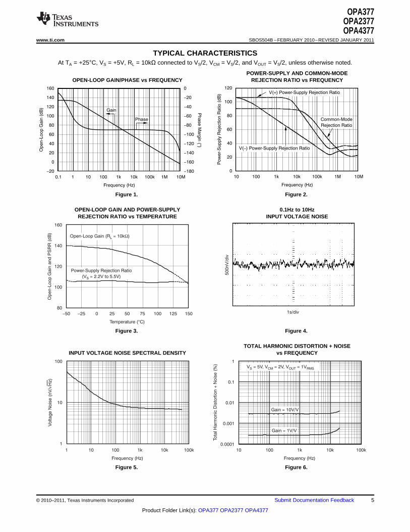
TYPICAL CHARACTERISTICSAt TA = +25°C, VS = +5V, RL = 10kΩ connected to VS/2, VCM = VS/2, and VOUT = VS/2, unless otherwise noted.
POWER-SUPPLY AND COMMON-MODEOPEN-LOOP GAIN/PHASE vs FREQUENCY REJECTION RATIO vs FREQUENCY
Figure 1. Figure 2.
OPEN-LOOP GAIN AND POWER-SUPPLY 0.1Hz to 10HzREJECTION RATIO vs TEMPERATURE INPUT VOLTAGE NOISE
Figure 3. Figure 4.
TOTAL HARMONIC DISTORTION + NOISEINPUT VOLTAGE NOISE SPECTRAL DENSITY vs FREQUENCY
Figure 5. Figure 6.
© 2010–2011, Texas Instruments Incorporated Submit Documentation Feedback 5
Product Folder Link(s): OPA377 OPA2377 OPA4377
Com
mon-M
ode R
eje
ction R
atio (
dB
)
-50 -25
110
100
90
80
70
60
50
Temperature ( C)°
15050 1000 25 75 125
Qu
iesce
nt
Cu
rre
nt
(A
)m
-50 -25
1000
900
800
700
600
500
Temperature ( C)°
15050 1000 25 75 125
Short
-Circuit C
urr
ent (m
A)
-50 -25
75
50
25
0
-25
-50
-75
-100
Temperature ( C)°
15050 1000 25 75 125
V = 2.75VS ±
ISC+
ISC-
Qu
iesce
nt
Cu
rre
nt
(A
)m
2.0 2.5
1000
900
800
700
600
500
Sh
ort-C
ircu
it Cu
rren
t (mA
)
50
40
30
20
10
0
Supply Voltage (V)
5.53.0 3.5 4.0 4.5 5.0
ISC+
IQ
Ou
tpu
t V
olta
ge
(V
)
0
3
2
1
0
-1
-2
-3
Output Current (mA)
8010 6020 30 40 50 70
+150 C° +125 C° +25 C° - °40 C
V = 2.75S ±
Input B
ias C
urr
ent (p
A)
-50 -25
Temperature ( C)°
15050 1000 25 75 125
1000
900
800
700
600
500
400
300
200
100
0
OPA377OPA2377OPA4377SBOS504B –FEBRUARY 2010–REVISED JANUARY 2011 www.ti.com
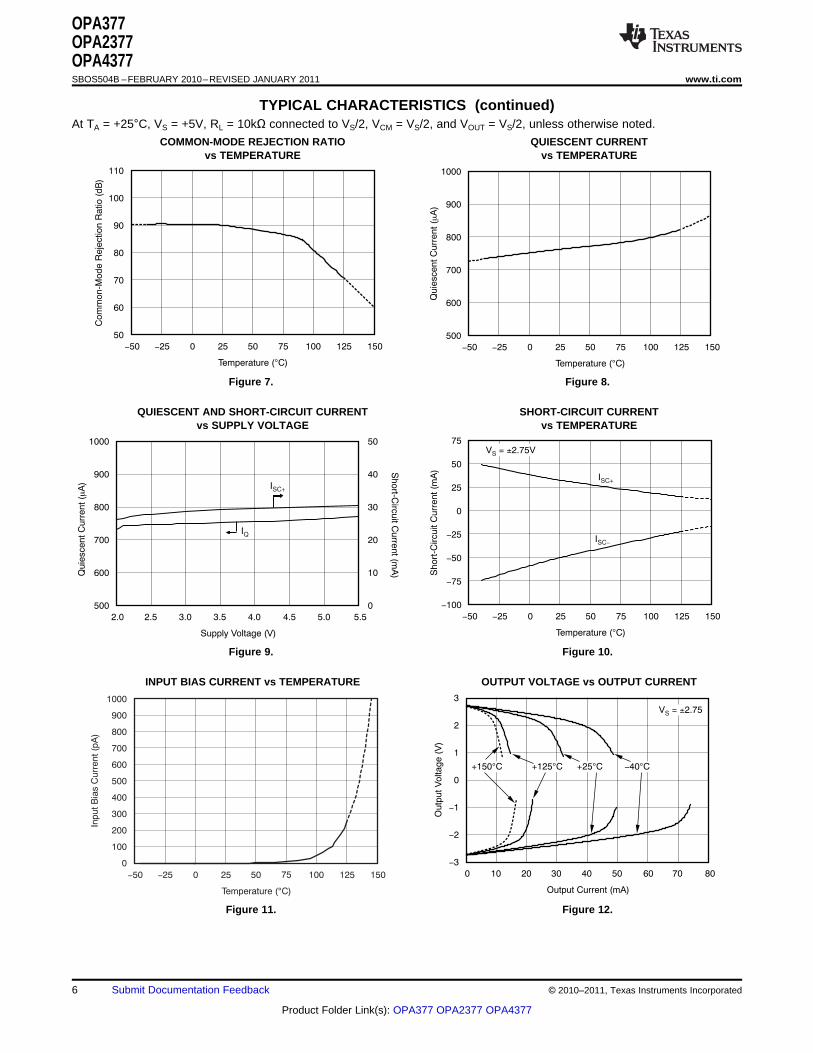
TYPICAL CHARACTERISTICS (continued)At TA = +25°C, VS = +5V, RL = 10kΩ connected to VS/2, VCM = VS/2, and VOUT = VS/2, unless otherwise noted.
COMMON-MODE REJECTION RATIO QUIESCENT CURRENTvs TEMPERATURE vs TEMPERATURE
Figure 7. Figure 8.
QUIESCENT AND SHORT-CIRCUIT CURRENT SHORT-CIRCUIT CURRENTvs SUPPLY VOLTAGE vs TEMPERATURE
Figure 9. Figure 10.
INPUT BIAS CURRENT vs TEMPERATURE OUTPUT VOLTAGE vs OUTPUT CURRENT
Figure 11. Figure 12.
6 Submit Documentation Feedback © 2010–2011, Texas Instruments Incorporated
Product Folder Link(s): OPA377 OPA2377 OPA4377
Ou
tpu
t V
olta
ge
(V
)P
P
1k
6
5
4
3
2
1
0
Frequency (Hz)
10M100k10k 1M
V = 5.5VS
V = 5VS
V = 2.5VS
Popula
tion
100
-100
200
-200
300
-300
400
-400
500
-500
600
-600
700
-700
800
-800
900
-900
1000
-1000
Offset Voltage ( V)m
0
50
mV
/div
Time (400ns/div)
G = +1
R = 10k
C
W
= 50pFL
L
Sm
all-
Sig
na
l O
ve
rsh
oo
t (%
)
10
50
40
30
20
10
0
Load Capacitance (pF)
1k100
G = +1V/V
1V
/div
Time (2 s/div)m
G = +1
R = 2kW
C = 50pFL
L
Se
ttlin
g T
ime
(s)
m
1
100
10
1
0.1
Closed-Loop Gain (V/V)
10010
0.01%
0.1%
OPA377OPA2377OPA4377
www.ti.com SBOS504B –FEBRUARY 2010–REVISED JANUARY 2011
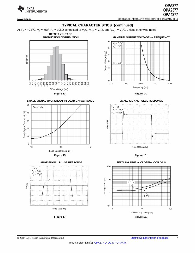
TYPICAL CHARACTERISTICS (continued)At TA = +25°C, VS = +5V, RL = 10kΩ connected to VS/2, VCM = VS/2, and VOUT = VS/2, unless otherwise noted.
OFFSET VOLTAGEPRODUCTION DISTRIBUTION MAXIMUM OUTPUT VOLTAGE vs FREQUENCY
Figure 13. Figure 14.
SMALL-SIGNAL OVERSHOOT vs LOAD CAPACITANCE SMALL-SIGNAL PULSE RESPONSE
Figure 15. Figure 16.
LARGE-SIGNAL PULSE RESPONSE SETTLING TIME vs CLOSED-LOOP GAIN
Figure 17. Figure 18.
© 2010–2011, Texas Instruments Incorporated Submit Documentation Feedback 7
Product Folder Link(s): OPA377 OPA2377 OPA4377
Channel S
epara
tion (
dB
)
10
140
120
100
80
60
40
0
Frequency (Hz)
100M1k100 10M10k 100k 1M
20
Open-L
oop O
utp
ut R
esis
tance (
)W
10
1k
100
10
1
0.1
Frequency (Hz)
10M1k100 10k 100k 1M
400 A Loadm
2mA Load
OPA377OPA2377OPA4377SBOS504B –FEBRUARY 2010–REVISED JANUARY 2011 www.ti.com
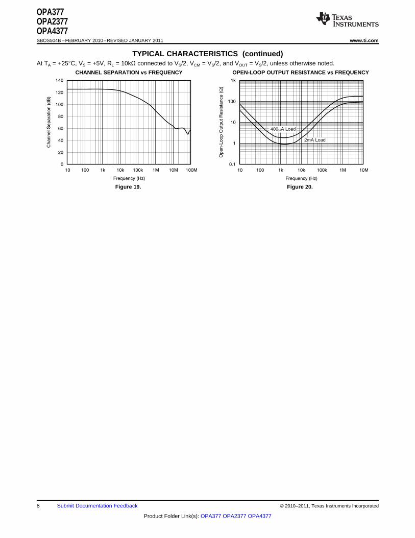
TYPICAL CHARACTERISTICS (continued)At TA = +25°C, VS = +5V, RL = 10kΩ connected to VS/2, VCM = VS/2, and VOUT = VS/2, unless otherwise noted.
CHANNEL SEPARATION vs FREQUENCY OPEN-LOOP OUTPUT RESISTANCE vs FREQUENCY
Figure 19. Figure 20.
8 Submit Documentation Feedback © 2010–2011, Texas Instruments Incorporated
Product Folder Link(s): OPA377 OPA2377 OPA4377
C1
100nF
R2
10kW
R1
1kW
+5V
VOUT
VIN
V = 2.5VCM
OPA377
Input O
ffset V
oltage (
mV
)
-0.5
3
2
1
0
-1
-2
-3
Input Common-Mode Voltage (V)
6.00 0.5 1.0 1.5 2.0 2.5 3.0 3.5 4.0 4.5 5.0 5.5
+V-V
OPA377OPA2377OPA4377
www.ti.com SBOS504B –FEBRUARY 2010–REVISED JANUARY 2011
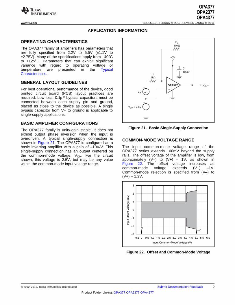
APPLICATION INFORMATION
OPERATING CHARACTERISTICS
The OPA377 family of amplifiers has parameters thatare fully specified from 2.2V to 5.5V (±1.1V to±2.75V). Many of the specifications apply from –40°Cto +125°C. Parameters that can exhibit significantvariance with regard to operating voltage ortemperature are presented in the TypicalCharacteristics.
GENERAL LAYOUT GUIDELINES
For best operational performance of the device, goodprinted circuit board (PCB) layout practices arerequired. Low-loss, 0.1mF bypass capacitors must beconnected between each supply pin and ground,placed as close to the device as possible. A singlebypass capacitor from V+ to ground is applicable tosingle-supply applications.
BASIC AMPLIFIER CONFIGURATIONSFigure 21. Basic Single-Supply ConnectionThe OPA377 family is unity-gain stable. It does not
exhibit output phase inversion when the input isoverdriven. A typical single-supply connection is COMMON-MODE VOLTAGE RANGEshown in Figure 21. The OPA377 is configured as a
The input common-mode voltage range of thebasic inverting amplifier with a gain of –10V/V. ThisOPA377 series extends 100mV beyond the supplysingle-supply connection has an output centered onrails. The offset voltage of the amplifier is low, fromthe common-mode voltage, VCM. For the circuitapproximately (V–) to (V+) – 1V, as shown inshown, this voltage is 2.5V, but may be any valueFigure 22. The offset voltage increases aswithin the common-mode input voltage range.common-mode voltage exceeds (V+) –1V.Common-mode rejection is specified from (V–) to(V+) – 1.3V.
Figure 22. Offset and Common-Mode Voltage
© 2010–2011, Texas Instruments Incorporated Submit Documentation Feedback 9
Product Folder Link(s): OPA377 OPA2377 OPA4377
5kW
OPA37710mA max
V+
VIN
VOUT
IOVERLOAD
10 toW
20W
V+
VIN
VOUT
RS
RL
CL
OPA377
OPA377OPA2377OPA4377SBOS504B –FEBRUARY 2010–REVISED JANUARY 2011 www.ti.com
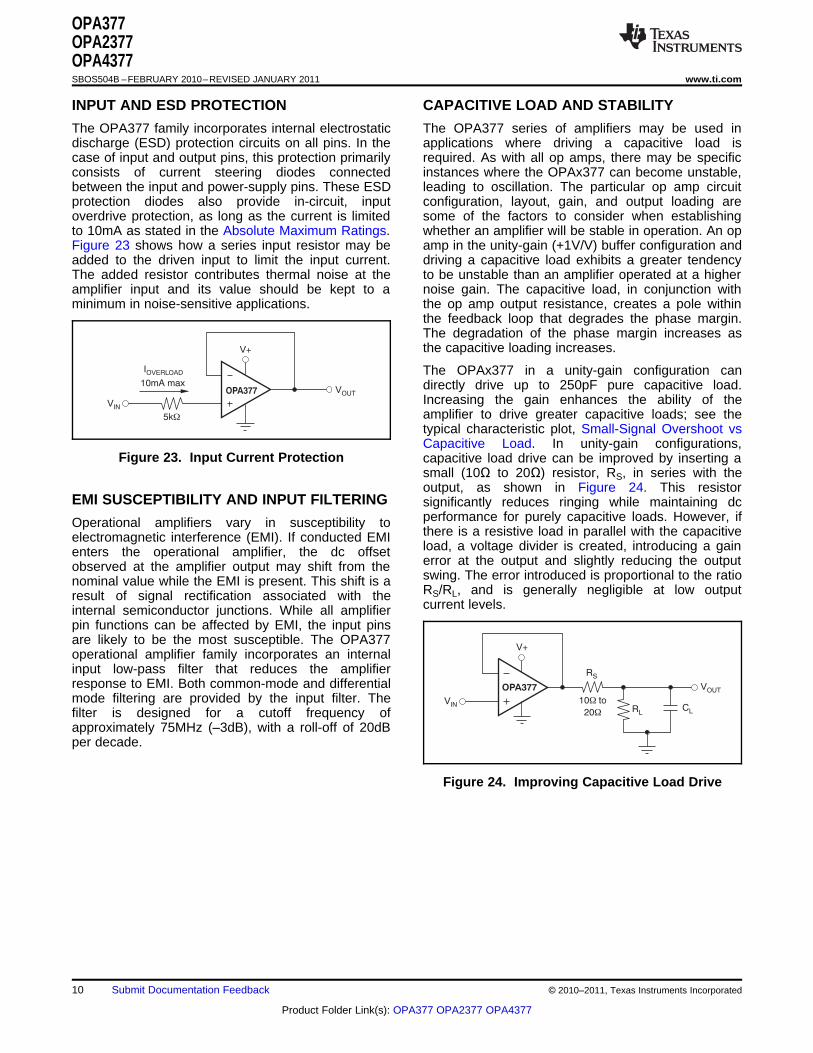
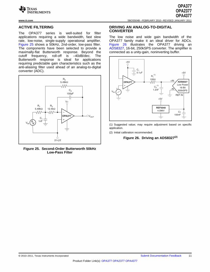
INPUT AND ESD PROTECTION CAPACITIVE LOAD AND STABILITY
The OPA377 family incorporates internal electrostatic The OPA377 series of amplifiers may be used indischarge (ESD) protection circuits on all pins. In the applications where driving a capacitive load iscase of input and output pins, this protection primarily required. As with all op amps, there may be specificconsists of current steering diodes connected instances where the OPAx377 can become unstable,between the input and power-supply pins. These ESD leading to oscillation. The particular op amp circuitprotection diodes also provide in-circuit, input configuration, layout, gain, and output loading areoverdrive protection, as long as the current is limited some of the factors to consider when establishingto 10mA as stated in the Absolute Maximum Ratings. whether an amplifier will be stable in operation. An opFigure 23 shows how a series input resistor may be amp in the unity-gain (+1V/V) buffer configuration andadded to the driven input to limit the input current. driving a capacitive load exhibits a greater tendencyThe added resistor contributes thermal noise at the to be unstable than an amplifier operated at a higheramplifier input and its value should be kept to a noise gain. The capacitive load, in conjunction withminimum in noise-sensitive applications. the op amp output resistance, creates a pole within
the feedback loop that degrades the phase margin.The degradation of the phase margin increases asthe capacitive loading increases.
The OPAx377 in a unity-gain configuration candirectly drive up to 250pF pure capacitive load.Increasing the gain enhances the ability of theamplifier to drive greater capacitive loads; see thetypical characteristic plot, Small-Signal Overshoot vsCapacitive Load. In unity-gain configurations,
Figure 23. Input Current Protection capacitive load drive can be improved by inserting asmall (10Ω to 20Ω) resistor, RS, in series with theoutput, as shown in Figure 24. This resistor
EMI SUSCEPTIBILITY AND INPUT FILTERING significantly reduces ringing while maintaining dcperformance for purely capacitive loads. However, ifOperational amplifiers vary in susceptibility tothere is a resistive load in parallel with the capacitiveelectromagnetic interference (EMI). If conducted EMIload, a voltage divider is created, introducing a gainenters the operational amplifier, the dc offseterror at the output and slightly reducing the outputobserved at the amplifier output may shift from theswing. The error introduced is proportional to the rationominal value while the EMI is present. This shift is aRS/RL, and is generally negligible at low outputresult of signal rectification associated with thecurrent levels.internal semiconductor junctions. While all amplifier
pin functions can be affected by EMI, the input pinsare likely to be the most susceptible. The OPA377operational amplifier family incorporates an internalinput low-pass filter that reduces the amplifierresponse to EMI. Both common-mode and differentialmode filtering are provided by the input filter. Thefilter is designed for a cutoff frequency ofapproximately 75MHz (–3dB), with a roll-off of 20dBper decade.
Figure 24. Improving Capacitive Load Drive
10 Submit Documentation Feedback © 2010–2011, Texas Instruments Incorporated
Product Folder Link(s): OPA377 OPA2377 OPA4377
C1
0.1 Fm
R
100W
1
(1)
+5V
VIN
ADS8327
Low Power
16-Bit
500kSPS
C3
(1)
1.2nF
C4
100nF
+5V
REF IN
-IN
+IN
REF5040
4.096V
+5V
OPA377
C1
1nF
C
150pF2
R3
5.49kW
R1
5.49kW
R2
12.4kW
V+
VOUT
VIN
OPA377
(V+)/2
OPA377OPA2377OPA4377
www.ti.com SBOS504B –FEBRUARY 2010–REVISED JANUARY 2011
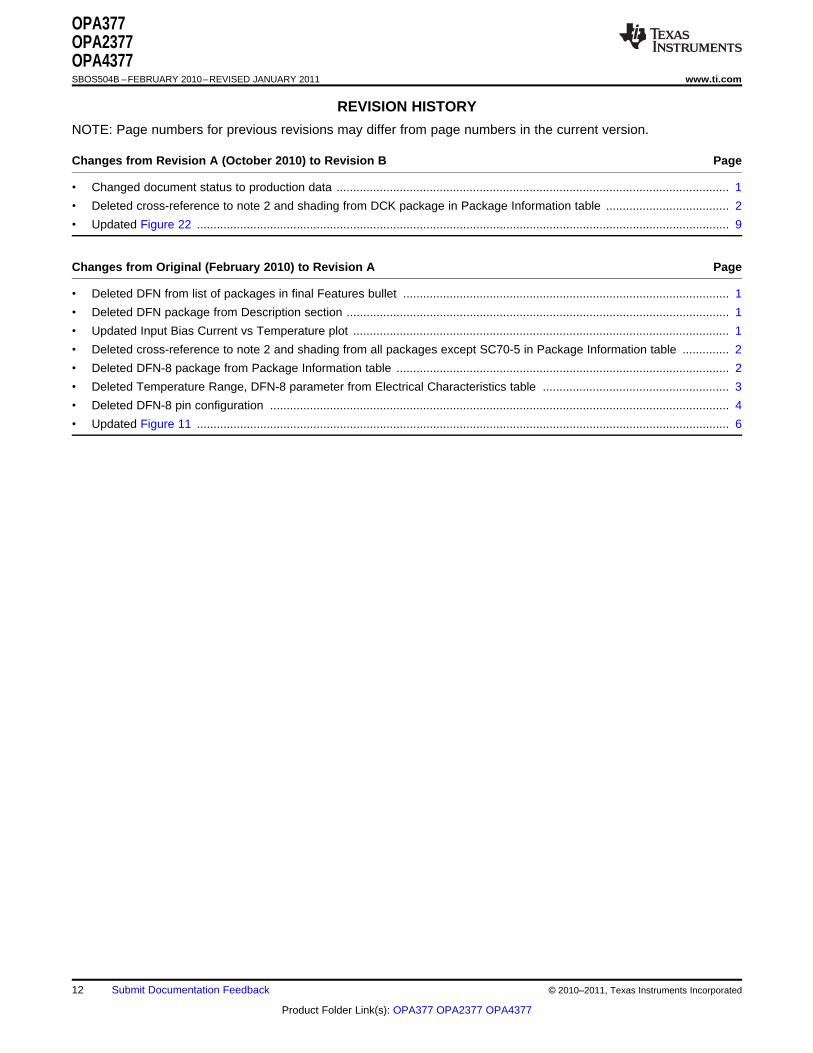
ACTIVE FILTERING DRIVING AN ANALOG-TO-DIGITALCONVERTER
The OPA377 series is well-suited for filterapplications requiring a wide bandwidth, fast slew The low noise and wide gain bandwidth of therate, low-noise, single-supply operational amplifier. OPA377 family make it an ideal driver for ADCs.Figure 25 shows a 50kHz, 2nd-order, low-pass filter. Figure 26 illustrates the OPA377 driving anThe components have been selected to provide a ADS8327, 16-bit, 250kSPS converter. The amplifier ismaximally-flat Butterworth response. Beyond the connected as a unity-gain, noninverting buffer.cutoff frequency, roll-off is –40dB/dec. TheButterworth response is ideal for applicationsrequiring predictable gain characteristics such as theanti-aliasing filter used ahead of an analog-to-digitalconverter (ADC).
(1) Suggested value; may require adjustment based on specificapplication.
(2) Initial calibration recommended.
Figure 26. Driving an ADS8327(2)
Figure 25. Second-Order Butterworth 50kHzLow-Pass Filter
© 2010–2011, Texas Instruments Incorporated Submit Documentation Feedback 11
Product Folder Link(s): OPA377 OPA2377 OPA4377
OPA377OPA2377OPA4377SBOS504B –FEBRUARY 2010–REVISED JANUARY 2011 www.ti.com
REVISION HISTORY
NOTE: Page numbers for previous revisions may differ from page numbers in the current version.
Changes from Revision A (October 2010) to Revision B Page
• Changed document status to production data ...................................................................................................................... 1
• Deleted cross-reference to note 2 and shading from DCK package in Package Information table ..................................... 2
• Updated Figure 22 ................................................................................................................................................................ 9
Changes from Original (February 2010) to Revision A Page
• Deleted DFN from list of packages in final Features bullet .................................................................................................. 1
• Deleted DFN package from Description section ................................................................................................................... 1
• Updated Input Bias Current vs Temperature plot ................................................................................................................. 1
• Deleted cross-reference to note 2 and shading from all packages except SC70-5 in Package Information table .............. 2
• Deleted DFN-8 package from Package Information table .................................................................................................... 2
• Deleted Temperature Range, DFN-8 parameter from Electrical Characteristics table ........................................................ 3
• Deleted DFN-8 pin configuration .......................................................................................................................................... 4
• Updated Figure 11 ................................................................................................................................................................ 6
12 Submit Documentation Feedback © 2010–2011, Texas Instruments Incorporated
Product Folder Link(s): OPA377 OPA2377 OPA4377
PACKAGE OPTION ADDENDUM
www.ti.com 18-Oct-2013
Addendum-Page 1
PACKAGING INFORMATION
Orderable Device Status(1)
Package Type PackageDrawing
Pins PackageQty
Eco Plan(2)
Lead/Ball Finish(6)
MSL Peak Temp(3)
Op Temp (°C) Device Marking(4/5)
Samples
OPA2377AID ACTIVE SOIC D 8 75 Green (RoHS& no Sb/Br)
CU NIPDAU Level-2-260C-1 YEAR -40 to 125 O2377A
OPA2377AIDGKR ACTIVE VSSOP DGK 8 2500 Green (RoHS& no Sb/Br)
CU NIPDAU |CU NIPDAUAG
Level-2-260C-1 YEAR -40 to 125 OTAQ
OPA2377AIDGKT ACTIVE VSSOP DGK 8 250 Green (RoHS& no Sb/Br)
CU NIPDAU |CU NIPDAUAG
Level-2-260C-1 YEAR -40 to 125 OTAQ
OPA2377AIDR ACTIVE SOIC D 8 2500 Green (RoHS& no Sb/Br)
CU NIPDAU Level-2-260C-1 YEAR -40 to 125 O2377A
OPA377AID ACTIVE SOIC D 8 75 Green (RoHS& no Sb/Br)
CU NIPDAU Level-2-260C-1 YEAR -40 to 125 OP377A
OPA377AIDBVR ACTIVE SOT-23 DBV 5 3000 Green (RoHS& no Sb/Br)
CU NIPDAU Level-2-260C-1 YEAR -40 to 125 PAG
OPA377AIDBVT ACTIVE SOT-23 DBV 5 250 Green (RoHS& no Sb/Br)
CU NIPDAU Level-2-260C-1 YEAR -40 to 125 PAG
OPA377AIDCKR ACTIVE SC70 DCK 5 3000 Green (RoHS& no Sb/Br)
CU NIPDAU Level-2-260C-1 YEAR -40 to 125 PAF
OPA377AIDCKT ACTIVE SC70 DCK 5 250 Green (RoHS& no Sb/Br)
CU NIPDAU Level-2-260C-1 YEAR -40 to 125 PAF
OPA377AIDR ACTIVE SOIC D 8 2500 Green (RoHS& no Sb/Br)
CU NIPDAU Level-2-260C-1 YEAR -40 to 125 OP377A
OPA4377AIPW ACTIVE TSSOP PW 14 90 Green (RoHS& no Sb/Br)
CU NIPDAU Level-2-260C-1 YEAR -40 to 125 OP4377A
OPA4377AIPWR ACTIVE TSSOP PW 14 2000 Green (RoHS& no Sb/Br)
CU NIPDAU Level-2-260C-1 YEAR -40 to 125 OP4377A
(1) The marketing status values are defined as follows:ACTIVE: Product device recommended for new designs.LIFEBUY: TI has announced that the device will be discontinued, and a lifetime-buy period is in effect.NRND: Not recommended for new designs. Device is in production to support existing customers, but TI does not recommend using this part in a new design.PREVIEW: Device has been announced but is not in production. Samples may or may not be available.OBSOLETE: TI has discontinued the production of the device.
(2) Eco Plan - The planned eco-friendly classification: Pb-Free (RoHS), Pb-Free (RoHS Exempt), or Green (RoHS & no Sb/Br) - please check http://www.ti.com/productcontent for the latest availabilityinformation and additional product content details.TBD: The Pb-Free/Green conversion plan has not been defined.
PACKAGE OPTION ADDENDUM
www.ti.com 18-Oct-2013
Addendum-Page 2
Pb-Free (RoHS): TI's terms "Lead-Free" or "Pb-Free" mean semiconductor products that are compatible with the current RoHS requirements for all 6 substances, including the requirement thatlead not exceed 0.1% by weight in homogeneous materials. Where designed to be soldered at high temperatures, TI Pb-Free products are suitable for use in specified lead-free processes.Pb-Free (RoHS Exempt): This component has a RoHS exemption for either 1) lead-based flip-chip solder bumps used between the die and package, or 2) lead-based die adhesive used betweenthe die and leadframe. The component is otherwise considered Pb-Free (RoHS compatible) as defined above.Green (RoHS & no Sb/Br): TI defines "Green" to mean Pb-Free (RoHS compatible), and free of Bromine (Br) and Antimony (Sb) based flame retardants (Br or Sb do not exceed 0.1% by weightin homogeneous material)
(3) MSL, Peak Temp. - The Moisture Sensitivity Level rating according to the JEDEC industry standard classifications, and peak solder temperature.
(4) There may be additional marking, which relates to the logo, the lot trace code information, or the environmental category on the device.
(5) Multiple Device Markings will be inside parentheses. Only one Device Marking contained in parentheses and separated by a "~" will appear on a device. If a line is indented then it is a continuationof the previous line and the two combined represent the entire Device Marking for that device.
(6) Lead/Ball Finish - Orderable Devices may have multiple material finish options. Finish options are separated by a vertical ruled line. Lead/Ball Finish values may wrap to two lines if the finishvalue exceeds the maximum column width.
Important Information and Disclaimer:The information provided on this page represents TI's knowledge and belief as of the date that it is provided. TI bases its knowledge and belief on informationprovided by third parties, and makes no representation or warranty as to the accuracy of such information. Efforts are underway to better integrate information from third parties. TI has taken andcontinues to take reasonable steps to provide representative and accurate information but may not have conducted destructive testing or chemical analysis on incoming materials and chemicals.TI and TI suppliers consider certain information to be proprietary, and thus CAS numbers and other limited information may not be available for release.
In no event shall TI's liability arising out of such information exceed the total purchase price of the TI part(s) at issue in this document sold by TI to Customer on an annual basis.
TAPE AND REEL INFORMATION
*All dimensions are nominal
Device PackageType
PackageDrawing
Pins SPQ ReelDiameter
(mm)
ReelWidth
W1 (mm)
A0(mm)
B0(mm)
K0(mm)
P1(mm)
W(mm)
Pin1Quadrant
OPA2377AIDGKR VSSOP DGK 8 2500 330.0 12.4 5.3 3.4 1.4 8.0 12.0 Q1
OPA2377AIDGKT VSSOP DGK 8 250 330.0 12.4 5.3 3.4 1.4 8.0 12.0 Q1
OPA2377AIDR SOIC D 8 2500 330.0 12.4 6.4 5.2 2.1 8.0 12.0 Q1
OPA377AIDBVR SOT-23 DBV 5 3000 180.0 8.4 3.23 3.17 1.37 4.0 8.0 Q3
OPA377AIDBVR SOT-23 DBV 5 3000 180.0 8.4 3.2 3.2 1.4 4.0 8.0 Q3
OPA377AIDBVT SOT-23 DBV 5 250 180.0 8.4 3.23 3.17 1.37 4.0 8.0 Q3
OPA377AIDBVT SOT-23 DBV 5 250 179.0 8.4 3.2 3.2 1.4 4.0 8.0 Q3
OPA377AIDCKR SC70 DCK 5 3000 179.0 8.4 2.2 2.5 1.2 4.0 8.0 Q3
OPA377AIDCKT SC70 DCK 5 250 179.0 8.4 2.2 2.5 1.2 4.0 8.0 Q3
OPA377AIDR SOIC D 8 2500 330.0 12.4 6.4 5.2 2.1 8.0 12.0 Q1
OPA4377AIPWR TSSOP PW 14 2000 330.0 12.4 6.9 5.6 1.6 8.0 12.0 Q1
PACKAGE MATERIALS INFORMATION
www.ti.com 8-May-2018
Pack Materials-Page 1
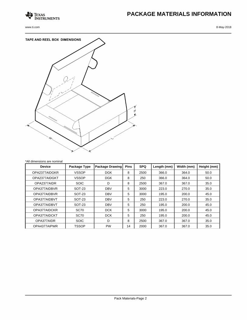
*All dimensions are nominal
Device Package Type Package Drawing Pins SPQ Length (mm) Width (mm) Height (mm)
OPA2377AIDGKR VSSOP DGK 8 2500 366.0 364.0 50.0
OPA2377AIDGKT VSSOP DGK 8 250 366.0 364.0 50.0
OPA2377AIDR SOIC D 8 2500 367.0 367.0 35.0
OPA377AIDBVR SOT-23 DBV 5 3000 223.0 270.0 35.0
OPA377AIDBVR SOT-23 DBV 5 3000 195.0 200.0 45.0
OPA377AIDBVT SOT-23 DBV 5 250 223.0 270.0 35.0
OPA377AIDBVT SOT-23 DBV 5 250 195.0 200.0 45.0
OPA377AIDCKR SC70 DCK 5 3000 195.0 200.0 45.0
OPA377AIDCKT SC70 DCK 5 250 195.0 200.0 45.0
OPA377AIDR SOIC D 8 2500 367.0 367.0 35.0
OPA4377AIPWR TSSOP PW 14 2000 367.0 367.0 35.0
PACKAGE MATERIALS INFORMATION
www.ti.com 8-May-2018
Pack Materials-Page 2
www.ti.com
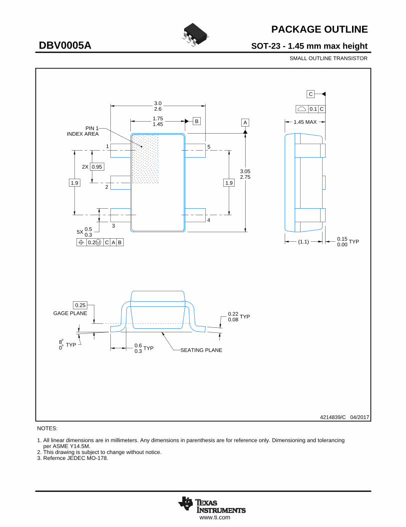
PACKAGE OUTLINE
C
TYP0.220.08
0.25
3.02.6
2X 0.95
1.9
1.45 MAX
TYP0.150.00
5X 0.50.3
TYP0.60.3
TYP80
1.9
A
3.052.75
B1.751.45
(1.1)
SOT-23 - 1.45 mm max heightDBV0005ASMALL OUTLINE TRANSISTOR
4214839/C 04/2017
NOTES: 1. All linear dimensions are in millimeters. Any dimensions in parenthesis are for reference only. Dimensioning and tolerancing per ASME Y14.5M.2. This drawing is subject to change without notice.3. Refernce JEDEC MO-178.
0.2 C A B
1
34
5
2
INDEX AREAPIN 1
GAGE PLANE
SEATING PLANE
0.1 C
SCALE 4.000
www.ti.com
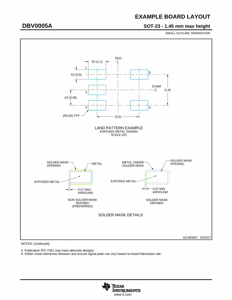
EXAMPLE BOARD LAYOUT
0.07 MAXARROUND
0.07 MINARROUND
5X (1.1)
5X (0.6)
(2.6)
(1.9)
2X (0.95)
(R0.05) TYP
4214839/C 04/2017
SOT-23 - 1.45 mm max heightDBV0005ASMALL OUTLINE TRANSISTOR
NOTES: (continued) 4. Publication IPC-7351 may have alternate designs. 5. Solder mask tolerances between and around signal pads can vary based on board fabrication site.
SYMM
LAND PATTERN EXAMPLEEXPOSED METAL SHOWN
SCALE:15X
PKG
1
3 4
5
2
SOLDER MASKOPENINGMETAL UNDER
SOLDER MASK
SOLDER MASKDEFINED
EXPOSED METAL
METALSOLDER MASKOPENING
NON SOLDER MASKDEFINED
(PREFERRED)
SOLDER MASK DETAILS
EXPOSED METAL
www.ti.com
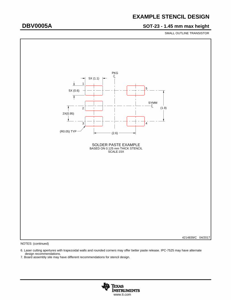
EXAMPLE STENCIL DESIGN
(2.6)
(1.9)
2X(0.95)
5X (1.1)
5X (0.6)
(R0.05) TYP
SOT-23 - 1.45 mm max heightDBV0005ASMALL OUTLINE TRANSISTOR
4214839/C 04/2017
NOTES: (continued) 6. Laser cutting apertures with trapezoidal walls and rounded corners may offer better paste release. IPC-7525 may have alternate design recommendations. 7. Board assembly site may have different recommendations for stencil design.
SOLDER PASTE EXAMPLEBASED ON 0.125 mm THICK STENCIL
SCALE:15X
SYMM
PKG
1
3 4
5
2
IMPORTANT NOTICE
Texas Instruments Incorporated (TI) reserves the right to make corrections, enhancements, improvements and other changes to itssemiconductor products and services per JESD46, latest issue, and to discontinue any product or service per JESD48, latest issue. Buyersshould obtain the latest relevant information before placing orders and should verify that such information is current and complete.TI’s published terms of sale for semiconductor products (http://www.ti.com/sc/docs/stdterms.htm) apply to the sale of packaged integratedcircuit products that TI has qualified and released to market. Additional terms may apply to the use or sale of other types of TI products andservices.Reproduction of significant portions of TI information in TI data sheets is permissible only if reproduction is without alteration and isaccompanied by all associated warranties, conditions, limitations, and notices. TI is not responsible or liable for such reproduceddocumentation. Information of third parties may be subject to additional restrictions. Resale of TI products or services with statementsdifferent from or beyond the parameters stated by TI for that product or service voids all express and any implied warranties for theassociated TI product or service and is an unfair and deceptive business practice. TI is not responsible or liable for any such statements.Buyers and others who are developing systems that incorporate TI products (collectively, “Designers”) understand and agree that Designersremain responsible for using their independent analysis, evaluation and judgment in designing their applications and that Designers havefull and exclusive responsibility to assure the safety of Designers' applications and compliance of their applications (and of all TI productsused in or for Designers’ applications) with all applicable regulations, laws and other applicable requirements. Designer represents that, withrespect to their applications, Designer has all the necessary expertise to create and implement safeguards that (1) anticipate dangerousconsequences of failures, (2) monitor failures and their consequences, and (3) lessen the likelihood of failures that might cause harm andtake appropriate actions. Designer agrees that prior to using or distributing any applications that include TI products, Designer willthoroughly test such applications and the functionality of such TI products as used in such applications.TI’s provision of technical, application or other design advice, quality characterization, reliability data or other services or information,including, but not limited to, reference designs and materials relating to evaluation modules, (collectively, “TI Resources”) are intended toassist designers who are developing applications that incorporate TI products; by downloading, accessing or using TI Resources in anyway, Designer (individually or, if Designer is acting on behalf of a company, Designer’s company) agrees to use any particular TI Resourcesolely for this purpose and subject to the terms of this Notice.TI’s provision of TI Resources does not expand or otherwise alter TI’s applicable published warranties or warranty disclaimers for TIproducts, and no additional obligations or liabilities arise from TI providing such TI Resources. TI reserves the right to make corrections,enhancements, improvements and other changes to its TI Resources. TI has not conducted any testing other than that specificallydescribed in the published documentation for a particular TI Resource.Designer is authorized to use, copy and modify any individual TI Resource only in connection with the development of applications thatinclude the TI product(s) identified in such TI Resource. NO OTHER LICENSE, EXPRESS OR IMPLIED, BY ESTOPPEL OR OTHERWISETO ANY OTHER TI INTELLECTUAL PROPERTY RIGHT, AND NO LICENSE TO ANY TECHNOLOGY OR INTELLECTUAL PROPERTYRIGHT OF TI OR ANY THIRD PARTY IS GRANTED HEREIN, including but not limited to any patent right, copyright, mask work right, orother intellectual property right relating to any combination, machine, or process in which TI products or services are used. Informationregarding or referencing third-party products or services does not constitute a license to use such products or services, or a warranty orendorsement thereof. Use of TI Resources may require a license from a third party under the patents or other intellectual property of thethird party, or a license from TI under the patents or other intellectual property of TI.TI RESOURCES ARE PROVIDED “AS IS” AND WITH ALL FAULTS. TI DISCLAIMS ALL OTHER WARRANTIES ORREPRESENTATIONS, EXPRESS OR IMPLIED, REGARDING RESOURCES OR USE THEREOF, INCLUDING BUT NOT LIMITED TOACCURACY OR COMPLETENESS, TITLE, ANY EPIDEMIC FAILURE WARRANTY AND ANY IMPLIED WARRANTIES OFMERCHANTABILITY, FITNESS FOR A PARTICULAR PURPOSE, AND NON-INFRINGEMENT OF ANY THIRD PARTY INTELLECTUALPROPERTY RIGHTS. TI SHALL NOT BE LIABLE FOR AND SHALL NOT DEFEND OR INDEMNIFY DESIGNER AGAINST ANY CLAIM,INCLUDING BUT NOT LIMITED TO ANY INFRINGEMENT CLAIM THAT RELATES TO OR IS BASED ON ANY COMBINATION OFPRODUCTS EVEN IF DESCRIBED IN TI RESOURCES OR OTHERWISE. IN NO EVENT SHALL TI BE LIABLE FOR ANY ACTUAL,DIRECT, SPECIAL, COLLATERAL, INDIRECT, PUNITIVE, INCIDENTAL, CONSEQUENTIAL OR EXEMPLARY DAMAGES INCONNECTION WITH OR ARISING OUT OF TI RESOURCES OR USE THEREOF, AND REGARDLESS OF WHETHER TI HAS BEENADVISED OF THE POSSIBILITY OF SUCH DAMAGES.Unless TI has explicitly designated an individual product as meeting the requirements of a particular industry standard (e.g., ISO/TS 16949and ISO 26262), TI is not responsible for any failure to meet such industry standard requirements.Where TI specifically promotes products as facilitating functional safety or as compliant with industry functional safety standards, suchproducts are intended to help enable customers to design and create their own applications that meet applicable functional safety standardsand requirements. Using products in an application does not by itself establish any safety features in the application. Designers mustensure compliance with safety-related requirements and standards applicable to their applications. Designer may not use any TI products inlife-critical medical equipment unless authorized officers of the parties have executed a special contract specifically governing such use.Life-critical medical equipment is medical equipment where failure of such equipment would cause serious bodily injury or death (e.g., lifesupport, pacemakers, defibrillators, heart pumps, neurostimulators, and implantables). Such equipment includes, without limitation, allmedical devices identified by the U.S. Food and Drug Administration as Class III devices and equivalent classifications outside the U.S.TI may expressly designate certain products as completing a particular qualification (e.g., Q100, Military Grade, or Enhanced Product).Designers agree that it has the necessary expertise to select the product with the appropriate qualification designation for their applicationsand that proper product selection is at Designers’ own risk. Designers are solely responsible for compliance with all legal and regulatoryrequirements in connection with such selection.Designer will fully indemnify TI and its representatives against any damages, costs, losses, and/or liabilities arising out of Designer’s non-compliance with the terms and provisions of this Notice.
Mailing Address: Texas Instruments, Post Office Box 655303, Dallas, Texas 75265Copyright © 2018, Texas Instruments Incorporated