Embed Size (px)
Citation preview
LM3900
AN-72 The LM3900: A New Current-Differencing Quad of Plus or Minus Input
Amplifiers
Literature Number: SNOA653
TL/H/7383
The
LM
3900:A
New
Curre
nt-D
iffere
ncin
gQ
uad
of
gIn
putA
mplifie
rsA
N-7
2
National SemiconductorApplication Note 72September 1972
The LM3900: A NewCurrent-Differencing Quadof g Input Amplifiers
PREFACE
With all the existing literature on ‘‘how to apply op amps’’ why should another application note be produced on this subject?
There are two answers to this question; 1) the LM3900 operates in quite an unusual manner (compared to a conventional op
amp) and therefore needs some explanation to familiarize a new user with this product, and 2) the standard op amp
applications assume a split power supply (g15 VDC) is available and our emphasis here is directed toward circuits for lower
cost single power supply control systems. Some of these circuits are simply ‘‘re-biased’’ versions of conventional handbook
circuits but many are new approaches which are made possible by some of the unique features of the LM3900.
Table of Contents
1.0 AN INTRODUCTION TO THE NEW ‘‘NORTON’’
AMPLIFIER
1.1 Basic Gain Stage
1.2 Obtaining a Non-inverting Input Function
1.3 The Complete Single-Supply Amplifier
2.0 INTRODUCTION TO APPLICATIONS OF THE LM3900
3.0 DESIGNING AC AMPLIFIERS
3.1 Single Power Supply Biasing
3.2 A Non-inverting Amplifier
3.3 ‘‘N VBE’’ Biasing
3.4 Biasing Using a Negative Supply
3.5 Obtaining High Input Impedance and High Gain
3.6 An Amplifier with a DC Gain Control
3.7 A Line-receiver Amplifier
4.0 DESIGNING DC AMPLIFIERS
4.1 Using Common-mode Biasing for VIN e 0 VDC
4.2 Adding an Output Diode for VO e 0 VDC
4.3 A DC Coupled Power Amplifier (IL s 3 Amps)
4.4 Ground Referencing a Differential Voltage
4.5 A Unity Gain Buffer Amplifier
5.0 DESIGNING VOLTAGE REGULATORS
5.1 Reducing the Input-output Voltage
5.2 Providing High Input Voltage Protection
5.3 High Input Voltage Protection and Low (VIN b VOUT)
5.4 Reducing Input Voltage Dependence and Adding
Short-Circuit Protection
6.0 DESIGNING RC ACTIVE FILTERS
6.1 Biasing the Amplifiers
6.2 A High Pass Active Filter
6.3 A Low Pass Active Filter
6.4 A Single-amplifier Bandpass Active Filter
6.5 A Two-amplifier Bandpass Active Filter
6.6 A Three-amplifier Bandpass Active Filter
6.7 Conclusions
7.0 DESIGNING WAVEFORM GENERATORS
7.1 Sinewave Oscillator
7.2 Squarewave Generator
7.0 DESIGNING WAVEFORM GENERATORS (Continued)
7.3 Pulse Generator
7.4 Triangle Waveform Generator
7.5 Sawtooth Waveform Generator
7.5.1 Generating a Very Slow Sawtooth Waveform
7.6 Staircase Waveform Generators
7.7 A Pulse Counter and a Voltage Variable
Pulse Counter
7.8 An Up-down Staircase Waveform Generator
8.0 DESIGNING PHASE-LOCKED LOOPS AND VOLTAGE
CONTROLLED OSCILLATORS
8.1 Voltage Controlled Oscillators (VCO)
8.2 Phase Comparator
8.3 A Complete Phase-locked Loop
8.4 Conclusions
9.0 DESIGNING DIGITAL AND SWITCHING CIRCUITS
9.1 An ‘‘OR’’ Gate
9.2 An ‘‘AND’’ Gate
9.3 A Bi-stable Multivibrator
9.4 Trigger Flip Flops
9.5 Monostable Multivibrators (One-shots)
9.5.1 A Two-amplifier One-shot
9.5.2 A Combination One-shot/Comparator Circuit
9.5.3 A One-amplifier One-shot (Positive Pulse)
9.5.4 A One-amplifier One-shot (Negative Pulse)
9.6 Comparators
9.6.1 A Comparator for Positive Input Voltages
9.6.2 A Comparator for Negative Input Voltages
9.6.3 A Power Comparator
9.6.4 A More Precise Comparator
9.7 Schmitt Triggers
10.0 SOME SPECIAL CIRCUIT APPLICATIONS
10.1 Current Sources and Sinks
10.1.1 A Fixed Current Source
10.1.2 A Voltage Variable Current Source
10.1.3 A Fixed Current Sink
10.1.4 A Voltage Variable Current Sink
C1995 National Semiconductor Corporation RRD-B30M115/Printed in U. S. A.

Table of Contents (Continued)
10.0 SOME SPECIAL CIRCUIT
APPLICATIONS (Continued)
10.2 Operation from g15 VDC Power Supplies
10.2.1 An AC Amplifier Operating with g15 VDCPower Supplies
10.2.2 A DC Amplifier Operating with g15 VDCPower Supplies
10.3 Tachometers
10.3.1 A Basic Tachometer
10.3.2 Extending VOUT (Minimum) to Ground
10.3.3 A Frequency Doubling Tachometer
10.4 A Squaring Amplifier
10.5 A Differentiator
10.6 A Difference Integrator
10.7 A Low Drift Sample and Hold Circuit
10.7.1 Reducing the ‘‘Effective’’ Input Biasing
Current
10.7.2 A Low Drift Ramp and Hold
10.7.3 Sample-Hold and Compare with New aVIN
10.0 SOME SPECIAL CIRCUIT
APPLICATIONS (Continued)
10.8 Audio Mixer or Channel Selector
10.9 A Low Frequency Mixer
10.10 A Peak Detector
10.11 Power Circuits
10.11.1 Lamp and/or Relay Drivers (s30 mA)
10.11.2 Lamp and/or Relay Drivers (s300 mA)
10.11.3 Positive Feedback Oscillators
10.12 High Voltage Operation
10.12.1 A High Voltage Inverting Amplifier
10.12.2 A High Voltage Non-inverting Amplifier
10.12.3 A Line Operated Audio Amplifier
10.13 Temperature Sensing
10.14 A ‘‘Programmable Unijunction’’
10.15 Adding a Differential Input Stage
List of Illustrations1 Basic Gain Stage
2 Adding a PNP Transistor to the Basic Gain Stage
3 Adding a Current Mirror to Achieve a Non-inverting Input
4 The Amplifier Stage
5 Open-loop Gain Characteristics
6 Schematic Diagram of the LM3900
7 An Equivalent Circuit of a Standard IC Op Amp
8 An Equivalent Circuit of the ‘‘Norton’’ Amplifier
9 Applying the LM3900 Equivalent Circuit
10 Biasing Equivalent Circuit
11 AC Equivalent Circuit
12 Inverting AC Amplifier Using Single-supply Biasing
13 Non-inverting AC Amplifier Using Voltage Reference Biasing
14 Inverting AC Amplifier Using N VBE Biasing
15 Negative Supply Biasing
16 A High ZIN High Gain Inverting AC Amplifier
17 An Amplifier with a DC Gain Control
18 A Line-receiver Amplifier
19 A DC Amplifier Employing Common-mode Biasing
20 An Ideal Circuit Model of a DC Amplifier with Zero Input Voltage
21 A Non-inverting DC Amplifier with Zero Volts Output for Zero Volts Input
22 Voltage Transfer Function for a DC Amplifier with a Voltage Gain of 10
23 A DC Power Amplifier
24 Ground Referencing a Differential Input DC Voltage
25 A Network to Invert and to Ground Reference a Negative DC Differential Input Voltage
26 A Unity-gain DC Buffer Amplifier
27 Simple Voltage Regulators
28 Reducing (VIN b VOUT)
29 High VIN Protection and Self-regulation
30 A High VIN Protected, Low (VIN b VOUT) Regulator
2
List of Illustrations (Continued)
31 Reducing VIN Dependence
32 Adding Short-Circuit Current Limiting
33 Biasing Considerations
34 A High Pass Active Filter
35 A Low Pass Active Filter
36 Biasing the Low Pass Filter
37 Biasing Equivalent Circuit
38 A One Op amp Bandpass Filter
39 A Two Op amp Bandpass Filter
40 The ‘‘Bi-quad’’ RC Active Bandpass Filter
41 A Sinewave Oscillator
42 A Squarewave Oscillator
43 A Pulse Generator
44 A Triangle Waveform Generator
45 Gated Sawtooth Generators
46 Generating Very Slow Sawtooth Waveforms
47 Pumping the Staircase Via Input Differentiator
48 A Free Running Staircase Generator
49 An Up-down Staircase Generator
50 A Voltage Controlled Oscillator
51 Adding Input Common-Mode Biasing Resistors
52 Reducing Temperature Drift
53 Improving Mark/Space Ratio
54 Phase Comparator
55 A Phase-Locked Loop
56 An ‘‘OR’’ Gate
57 An ‘‘AND’’ Gate
58 A Large Fan-in ‘‘AND’’ Gate
59 A Bi-Stable Multivibrator
60 A Trigger Flip Flop
61 A Two-amplifier Trigger Flip Flop
62 A One-Shot Multivibrator
63 A One-Shot Multivibrator with an Input Comparator
64 A One-Amplifier One-Shot (Positive Output)
65 A One-Amplifier One-Shot (Negative Output)
66 An Inverting Voltage Comparator
67 A Non-Inverting Low-voltage Comparator
68 A Non-Inverting Power Comparator
69 A More Precise Comparator
70 Schmitt Triggers
71 Fixed Current Sources
72 A Voltage Controlled Current Source
73 Fixed Current Sinks
74 A Voltage Controlled Current Sink
75 An AC Amplifier Operating with g15 VDC
76 DC Biasing for g15 VDC Operation
77 A DC Amplifier Operating with g15 VDC
78 A Basic Tachometer
79 Adding Biasing to Provide VO e 0 VDC
80 A Frequency Doubling Tachometer
81 A Squaring Amplifier with Hysteresis
82 A Differentiator Circuit
83 A Difference Integrator
3

List of Illustrations (Continued)
84 Reducing IB ‘‘Effective’’to Zero
85 A Low-Drift Ramp and Hold Circuit
86 Sample-Hold and Compare with New aVIN
87 Audio Mixing or Selection
88 A Low Frequency Mixer
89 A Peak Detector
90 Sinking 20 to 30 mA Loads
91 Boosting to 300 mA Loads
92 Positive Feedback Power Oscillators
93 A High Voltage Inverting Amplifier
94 A High Voltage Non-Inverting Amplifier
95 A Line Operated Audio Amplifier
96 Temperature Sensing
97 A ‘‘Programmable Unijunction’’
98 Adding a Differential Input Stage
4
The LM3900: A New Current-DifferencingQuad of g Input Amplifiers
1.0 An Introduction to the New‘‘Norton’’ AmplifierThe LM3900 represents a departure from conventional am-
plifier designs. Instead of using a standard transistor differ-
ential amplifier at the input, the non-inverting input function
has been achieved by making use of a ‘‘current-mirror’’ to
‘‘mirror’’ the non-inverting input current about ground and
then to extract this current from that which is entering the
inverting input terminal. Whereas the conventional op amp
differences input voltages, this amplifier differences input
currents and therefore the name ‘‘Norton Amp’’ has been
used to indicate this new type of operation. Many biasing
advantages are realized when operating with only a single
power supply voltage. The fact that currents can be passed
between the input terminals allows some unusual applica-
tions. If external, large valued input resistors are used (to
convert from input voltages to input currents) most of the
standard op amp applications can be realized.
Many industrial electronic control systems are designed that
operate off of only a single power supply voltage. The con-
ventional integrated-circuit operational amplifier (IC op amp)
is typically designed for split power supplies (g15 VDC) and
suffers from a poor output voltage swing and a rather large
minimum common-mode input voltage range (approximatelya 2 VDC) when used in a single power supply application. In
addition, some of the performance characteristics of these
op amps could be sacrificedÐespecially in favor of reduced
costs.
To meet the needs of the designers of low-cost, single-pow-
er-supply control systems, a new internally compensated
amplifier has been designed that operates over a power
supply voltage range of a4 VDC to 36 VDC with small
changes in performance characteristics and provides an
output peak-to-peak voltage swing that is only 1V less than
the magnitude of the power supply voltage. Four of these
amplifiers have been fabricated on a single chip and are
provided in the standard 14-pin dual-in-line package.
The cost, application and performance advantages of this
new quad amplifier will guarantee it a place in many single
power supply electronic systems. Many of the ‘‘housekeep-
ing’’ applications which are now handled by standard IC op
amps can also be handled by this ‘‘Norton’’ amplifier operat-
ing off the existing g15 VDC power supplies.
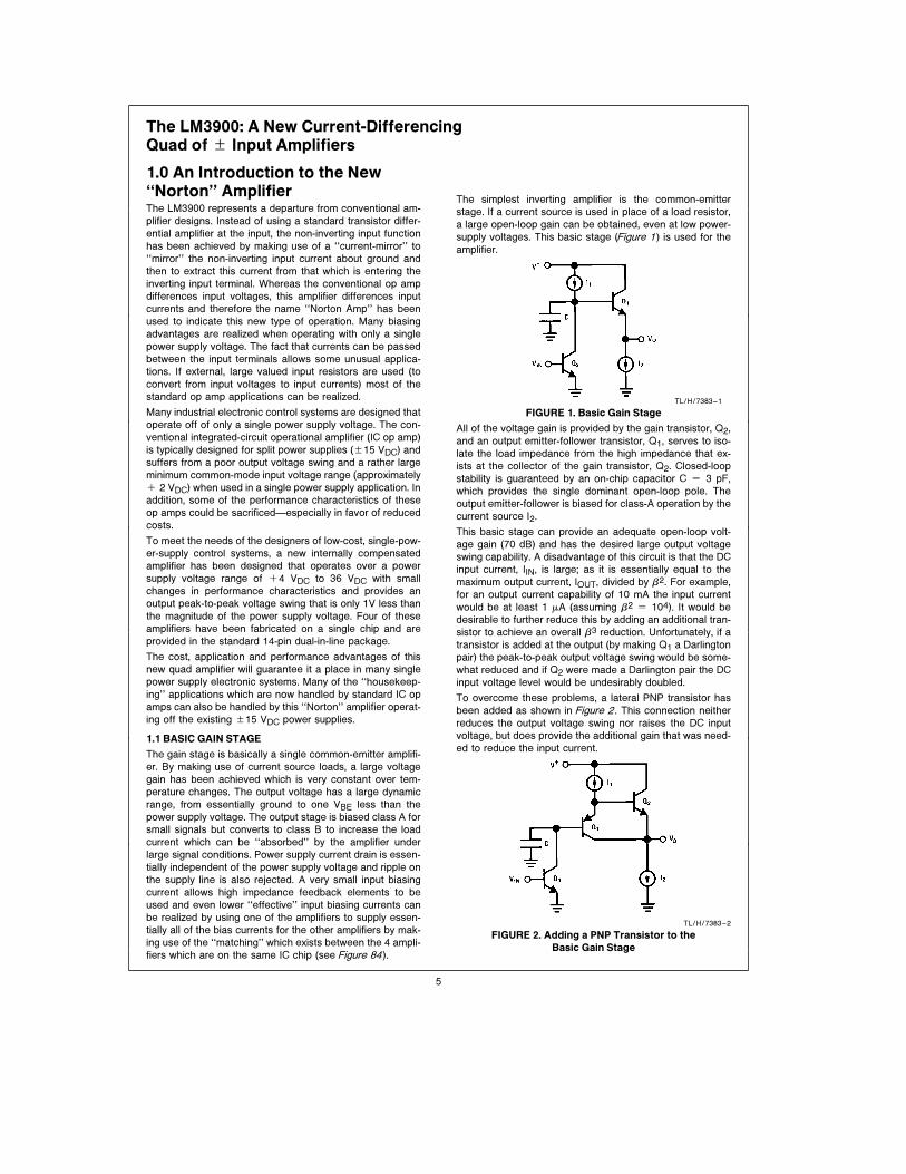
1.1 BASIC GAIN STAGE
The gain stage is basically a single common-emitter amplifi-
er. By making use of current source loads, a large voltage
gain has been achieved which is very constant over tem-
perature changes. The output voltage has a large dynamic
range, from essentially ground to one VBE less than the
power supply voltage. The output stage is biased class A for
small signals but converts to class B to increase the load
current which can be ‘‘absorbed’’ by the amplifier under
large signal conditions. Power supply current drain is essen-
tially independent of the power supply voltage and ripple on
the supply line is also rejected. A very small input biasing
current allows high impedance feedback elements to be
used and even lower ‘‘effective’’ input biasing currents can
be realized by using one of the amplifiers to supply essen-
tially all of the bias currents for the other amplifiers by mak-
ing use of the ‘‘matching’’ which exists between the 4 ampli-
fiers which are on the same IC chip (see Figure 84).
The simplest inverting amplifier is the common-emitter
stage. If a current source is used in place of a load resistor,
a large open-loop gain can be obtained, even at low power-
supply voltages. This basic stage (Figure 1) is used for the
amplifier.
TL/H/7383–1
FIGURE 1. Basic Gain Stage
All of the voltage gain is provided by the gain transistor, Q2,
and an output emitter-follower transistor, Q1, serves to iso-
late the load impedance from the high impedance that ex-
ists at the collector of the gain transistor, Q2. Closed-loop
stability is guaranteed by an on-chip capacitor C e 3 pF,
which provides the single dominant open-loop pole. The
output emitter-follower is biased for class-A operation by the
current source I2.
This basic stage can provide an adequate open-loop volt-
age gain (70 dB) and has the desired large output voltage
swing capability. A disadvantage of this circuit is that the DC
input current, IIN, is large; as it is essentially equal to the
maximum output current, IOUT, divided by b2. For example,
for an output current capability of 10 mA the input current
would be at least 1 mA (assuming b2 e 104). It would be
desirable to further reduce this by adding an additional tran-
sistor to achieve an overall b3 reduction. Unfortunately, if a
transistor is added at the output (by making Q1 a Darlington
pair) the peak-to-peak output voltage swing would be some-
what reduced and if Q2 were made a Darlington pair the DC
input voltage level would be undesirably doubled.
To overcome these problems, a lateral PNP transistor has
been added as shown in Figure 2. This connection neither
reduces the output voltage swing nor raises the DC input
voltage, but does provide the additional gain that was need-
ed to reduce the input current.
TL/H/7383–2
FIGURE 2. Adding a PNP Transistor to the
Basic Gain Stage
5
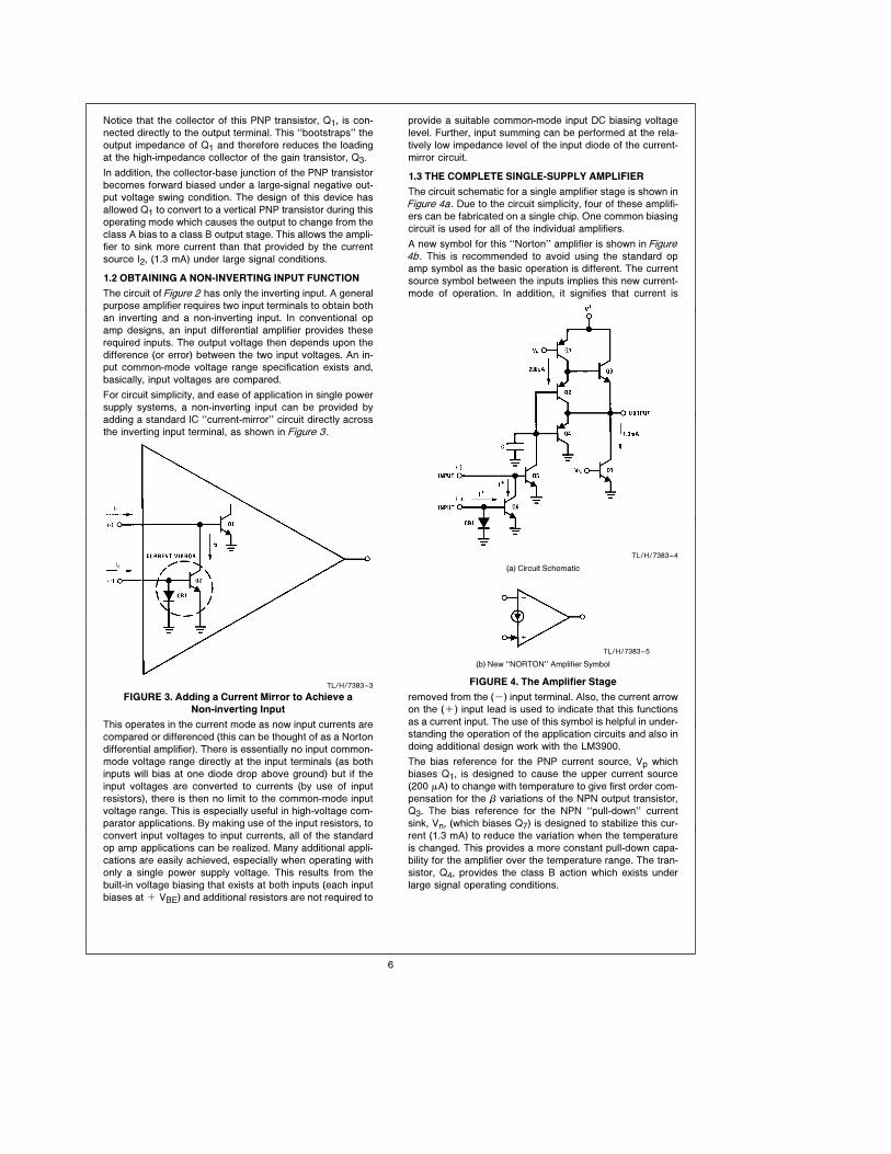
Notice that the collector of this PNP transistor, Q1, is con-
nected directly to the output terminal. This ‘‘bootstraps’’ the
output impedance of Q1 and therefore reduces the loading
at the high-impedance collector of the gain transistor, Q3.
In addition, the collector-base junction of the PNP transistor
becomes forward biased under a large-signal negative out-
put voltage swing condition. The design of this device has
allowed Q1 to convert to a vertical PNP transistor during this
operating mode which causes the output to change from the
class A bias to a class B output stage. This allows the ampli-
fier to sink more current than that provided by the current
source I2, (1.3 mA) under large signal conditions.
1.2 OBTAINING A NON-INVERTING INPUT FUNCTION
The circuit of Figure 2 has only the inverting input. A general
purpose amplifier requires two input terminals to obtain both
an inverting and a non-inverting input. In conventional op
amp designs, an input differential amplifier provides these
required inputs. The output voltage then depends upon the
difference (or error) between the two input voltages. An in-
put common-mode voltage range specification exists and,
basically, input voltages are compared.
For circuit simplicity, and ease of application in single power
supply systems, a non-inverting input can be provided by
adding a standard IC ‘‘current-mirror’’ circuit directly across
the inverting input terminal, as shown in Figure 3.
TL/H/7383–3
FIGURE 3. Adding a Current Mirror to Achieve a
Non-inverting Input
This operates in the current mode as now input currents are
compared or differenced (this can be thought of as a Norton
differential amplifier). There is essentially no input common-
mode voltage range directly at the input terminals (as both
inputs will bias at one diode drop above ground) but if the
input voltages are converted to currents (by use of input
resistors), there is then no limit to the common-mode input
voltage range. This is especially useful in high-voltage com-
parator applications. By making use of the input resistors, to
convert input voltages to input currents, all of the standard
op amp applications can be realized. Many additional appli-
cations are easily achieved, especially when operating with
only a single power supply voltage. This results from the
built-in voltage biasing that exists at both inputs (each input
biases at a VBE) and additional resistors are not required to
provide a suitable common-mode input DC biasing voltage
level. Further, input summing can be performed at the rela-
tively low impedance level of the input diode of the current-
mirror circuit.
1.3 THE COMPLETE SINGLE-SUPPLY AMPLIFIER
The circuit schematic for a single amplifier stage is shown in
Figure 4a. Due to the circuit simplicity, four of these amplifi-
ers can be fabricated on a single chip. One common biasing
circuit is used for all of the individual amplifiers.
A new symbol for this ‘‘Norton’’ amplifier is shown in Figure4b. This is recommended to avoid using the standard op
amp symbol as the basic operation is different. The current
source symbol between the inputs implies this new current-
mode of operation. In addition, it signifies that current is
TL/H/7383–4
(a) Circuit Schematic
TL/H/7383–5
(b) New ‘‘NORTON’’ Amplifier Symbol
FIGURE 4. The Amplifier Stage
removed from the (b) input terminal. Also, the current arrow
on the (a) input lead is used to indicate that this functions
as a current input. The use of this symbol is helpful in under-
standing the operation of the application circuits and also in
doing additional design work with the LM3900.
The bias reference for the PNP current source, Vp which
biases Q1, is designed to cause the upper current source
(200 mA) to change with temperature to give first order com-
pensation for the b variations of the NPN output transistor,
Q3. The bias reference for the NPN ‘‘pull-down’’ current
sink, Vn, (which biases Q7) is designed to stabilize this cur-
rent (1.3 mA) to reduce the variation when the temperature
is changed. This provides a more constant pull-down capa-
bility for the amplifier over the temperature range. The tran-
sistor, Q4, provides the class B action which exists under
large signal operating conditions.
6

The performance characteristics of each amplifier stage are
summarized below:
Power-supply voltage range ÀÀÀÀÀÀÀÀÀÀÀÀÀÀÀ4 to 36 VDC org2 to g18 VDC
Bias current drain per amplifier
stage ÀÀÀÀÀÀÀÀÀÀÀÀÀÀÀÀÀÀÀÀÀÀÀÀÀÀÀÀÀÀÀÀÀÀÀÀÀ1.3 mADC
Open loop:
Voltage gain (RL e 10k) ÀÀÀÀÀÀÀÀÀÀÀÀÀÀÀÀÀÀÀÀÀÀÀÀ70 dB
Unity-gain frequency ÀÀÀÀÀÀÀÀÀÀÀÀÀÀÀÀÀÀÀÀÀÀÀÀÀ2.5 MHz
Phase marginÀÀÀÀÀÀÀÀÀÀÀÀÀÀÀÀÀÀÀÀÀÀÀÀÀÀÀÀÀÀÀÀÀÀÀÀ40§Input resistanceÀÀÀÀÀÀÀÀÀÀÀÀÀÀÀÀÀÀÀÀÀÀÀÀÀÀÀÀÀÀÀÀ1 MX
Output resistanceÀÀÀÀÀÀÀÀÀÀÀÀÀÀÀÀÀÀÀÀÀÀÀÀÀÀÀÀÀÀÀ8 kX
Output voltage swing ÀÀÀÀÀÀÀÀÀÀÀÀÀÀÀÀÀÀÀÀÀ(VCC b 1) Vpp
Input bias currentÀÀÀÀÀÀÀÀÀÀÀÀÀÀÀÀÀÀÀÀÀÀÀÀÀÀÀÀÀÀ30 nADC
Slew rate ÀÀÀÀÀÀÀÀÀÀÀÀÀÀÀÀÀÀÀÀÀÀÀÀÀÀÀÀÀÀÀÀÀÀÀÀÀ0.5V/ms
As the bias currents are all derived from diode forward volt-
age drops, there is only a small change in bias current mag-
nitude as the power-supply voltage is varied. The open-loop
gain changes only slightly over the complete power supply
voltage range and is essentially independent of temperature
changes. The open-loop frequency response is compared
with the ‘‘741’’ op amp in Figure 5. The higher unity-gain
crossover frequency is seen to provide an additional 10 dB
of gain for all frequencies greater than 1 kHz.
TL/H/7383–6
FIGURE 5. Open-loop Gain Characteristics
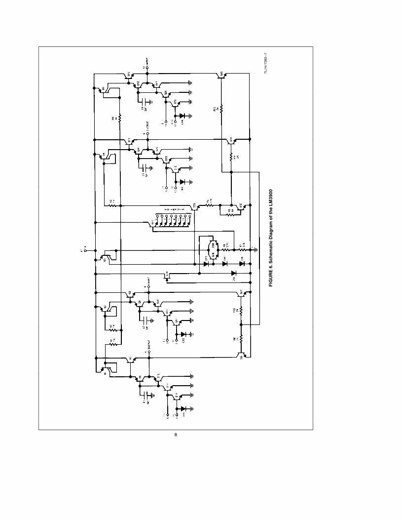
The complete schematic diagram of the LM3900 is shown in
Figure 6. The one resistor, R5, establishes the power con-
sumption of the circuit as it controls the conduction of tran-
sistor Q28. The emitter current of Q28 is used to bias the
NPN output class-A biasing current sources and the collec-
tor current of Q28 is the reference for the PNP current
source of each amplifier.
The biasing circuit is initially ‘‘started’’ by Q20, Q30 and CR6.
After start-up is achieved, Q30 goes OFF and the current
flow through the reference diodes: CR5, CR7 and CR8, is
dependent only on VBE/(R6 a R7). This guarantees that
the power supply current drain is essentially independent of
the magnitude of the power supply voltage.
The input clamp for negative voltages is provided by the
multi-emitter NPN transistor Q21. One of the emitters of this
transistor goes to each of the input terminals. The reference
voltage for the base of Q21 is provided by R6 and R7 and is
approximately VBE/2.
2.0 Introduction to Applications ofthe LM3900Like the standard IC op amp, the LM3900 has a wide range
of applications. A new approach must be taken to design
circuits with this ‘‘Norton’’ amplifier and the object of this
note is to present a variety of useful circuits to indicate how
conventional and unique new applications can be de-
signedÐespecially when operating with only a single power
supply voltage.
To understand the operation of the LM3900 we will com-
pare it with the more familiar standard IC op amp. When
operating on a single power supply voltage, the minimum
input common-mode voltage range of a standard op amp
limits the smallest value of voltage which can be applied to
both inputs and still have the amplifier respond to a differen-
tial input signal. In addition, the output voltage will not swing
completely from ground to the power supply voltage. The
output voltage depends upon the difference between the
input voltages and a bias current must be supplied to both
inputs. A simplified diagram of a standard IC op amp operat-
ing from a single power supply is shown inFigure 7. The (a)
and (b) inputs go only to current sources and therefore are
free to be biased or operated at any voltage values which
are within the input common-mode voltage range. The cur-
rent sources at the input terminals, IBa and IB
b, represent
the bias currents which must be supplied to both of the input
transistors of the op amp (base currents). The output circuit
is modeled as an active voltage source which depends upon
the open-loop gain of the amplifier, Av, and the difference
which exists between the input voltages, (Va b Vb).
TL/H/7383–8
FIGURE 7. An Equivalent Circuit of a Standard
IC Op Amp
An equivalent circuit for the ‘‘Norton’’ amplifier is shown in
Figure 8. The (a) and (b) inputs are both clamped by di-
odes to force them to be one-diode drop above groundÐal-
ways! They are not free to move and the ‘‘input common-
mode voltage range’’ directly at these input terminals is very
smallÐa few hundred mV centered about 0.5 VDC. This is
TL/H/7383–9
FIGURE 8. An Equivalent Circuit of the
‘‘Norton’’ Amplifier
7
TL/H
/7383–7
FIG
UR
E6.Schem
atic
Dia
gra
mofth
eLM
3900
8
why external voltages must be first converted to currents
(using resistors) before being applied to the inputsÐand is
the basis for the current-mode (or Norton) type of operation.
With external input resistorsÐthere is no limit to the ‘‘input
common-mode voltage range’’. The diode shown across the
(a) input actually exists as a diode in the circuit and the
diode across the (b) input is used to model the base-emit-
ter junction of the transistor which exists at this input.
Only the (b) input must be supplied with a DC biasing cur-
rent, IB. The (a) input couples only to the (b) input and
then to extract from this (b) input terminal the same current
(AI, the mirror gain, is approximately equal to 1) which is
entered (by the external circuitry) into the (a) input terminal.
This operation is described as a ‘‘current-mirror’’ as the cur-
rent entering the (a) input is ‘‘mirrored’’ or ‘‘reflected’’
about ground and is then extracted from the (b) input.
There is a maximum or near saturation value of current
which the ‘‘mirror’’ at the (a) input can handle. This is listed
on the data sheet as ‘‘maximum mirror current’’ and ranges
from approximately 6 mA at 25§C to 3.8 mA at 70§C.
This fact that the (a) input current modulates or affects the
(b) input current causes this amplifier to pass currents be-
tween the input terminals and is the basis for many new
application circuitsÐespecially when operating with only a
single power supply voltage.
The output is modeled as an active voltage source which
also depends upon the open-loop voltage gain, Av, but only
the (b) input voltage, Vb, (not the differential input volt-
age). Finally, the output voltage of the LM3900 can swing
from essentially ground (a90 mV) to within one VBE of the
power supply voltage.
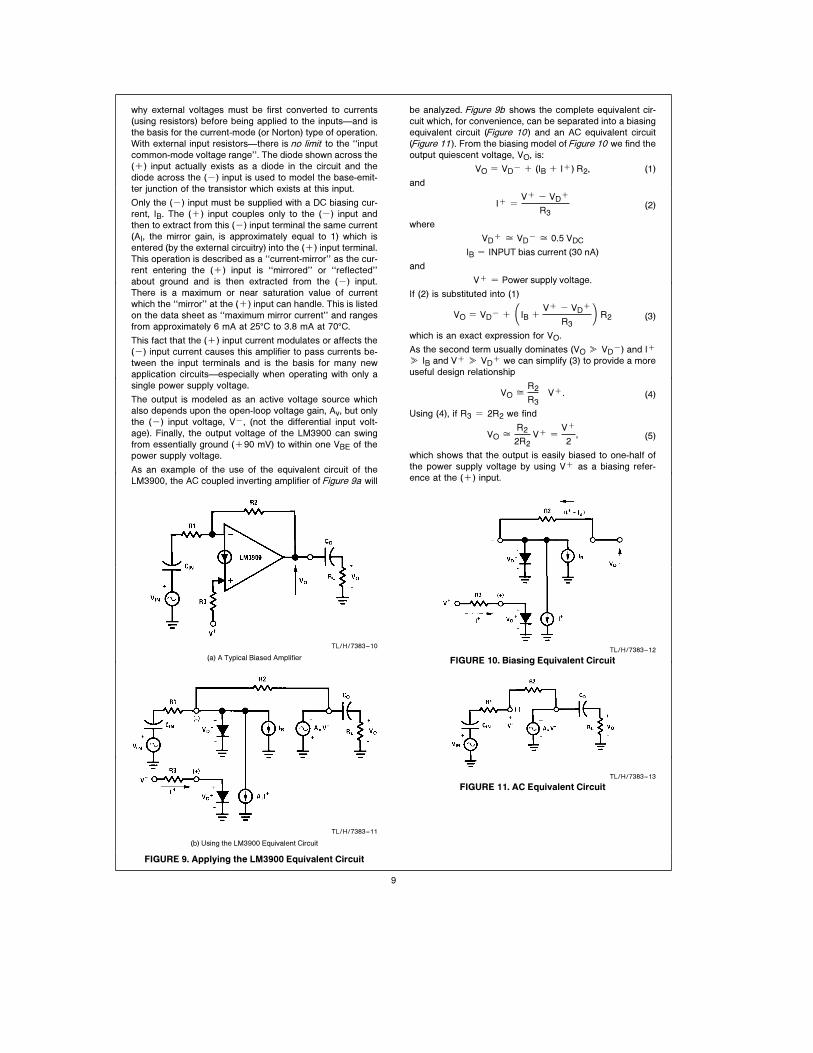
As an example of the use of the equivalent circuit of the
LM3900, the AC coupled inverting amplifier of Figure 9a will
be analyzed. Figure 9b shows the complete equivalent cir-
cuit which, for convenience, can be separated into a biasing
equivalent circuit (Figure 10) and an AC equivalent circuit
(Figure 11). From the biasing model of Figure 10 we find the
output quiescent voltage, VO, is:
VO e VDb a (IB a Ia) R2, (1)
and
Ia e
Va b VDa
R3(2)
where
VDa j VD
b j 0.5 VDC
IB e INPUT bias current (30 nA)
and
Va e Power supply voltage.
If (2) is substituted into (1)
VO e VDb a # IB a
Va b VDa
R3 J R2 (3)
which is an exact expression for VO.
As the second term usually dominates (VO n VDb) and Ia
n IB and Va n VDa we can simplify (3) to provide a more
useful design relationship
VO jR2
R3Va. (4)
Using (4), if R3 e 2R2 we find
VO jR2
2R2Va e
Va
2, (5)
which shows that the output is easily biased to one-half of
the power supply voltage by using Va as a biasing refer-
ence at the (a) input.
TL/H/7383–10
(a) A Typical Biased Amplifier
TL/H/7383–11
(b) Using the LM3900 Equivalent Circuit
FIGURE 9. Applying the LM3900 Equivalent Circuit
TL/H/7383–12
FIGURE 10. Biasing Equivalent Circuit
TL/H/7383–13
FIGURE 11. AC Equivalent Circuit
9

The AC equivalent circuit of Figure 11 is the same as that
which would result if a standard IC op amp were used with
the (a) input grounded. The closed-loop voltage gain AvCL,
is given by:
AvCLA
VO
VIN
j b
R2
R1(6)
if Av (open-loop) l
R2
R1.
The design procedure for an AC coupled inverting amplifier
using the LM3900 is therefore to first select R1, CIN, R2, and
CO as with a standard IC op amp and then to simply add R3e 2R2 as a final biasing consideration. Other biasing tech-
niques are presented in the following sections of this note.
For the switching circuit applications, the biasing model of
Figure 10 is adequate to predict circuit operation.
Although the LM3900 has four independent amplifiers, the
use of the label ‘‘(/4LM3900’’ will be shortened to simply
‘‘LM3900’’ for the application drawings contained in this
note.
3.0 Designing AC AmplifiersThe LM3900 readily lends itself to use as an AC amplifier
because the output can be biased to any desired DC level
within the range of the output voltage swing and the AC gain
is independent of the biasing network. In addition, the single
power supply requirement makes the LM3900 attractive for
any low frequency gain application. For lowest noise per-
formance, the (a) input should be grounded (Figure 9a) and
the output will then bias at aVBE. Although the LM3900 is
not suitable as an ultra low noise tape pre-amp, it is useful in
most other applications. The restriction to only shunt feed-
back causes a small input impedance. Transducers which
can be loaded can operate with this low input impedance.
The noise degradation which would result from the use of a
large input resistor limits the usefulness where low noise
and high input impedance are both required.
3.1 SINGLE POWER SUPPLY BIASING
The LM3900 can be biased in several different ways. The
circuit inFigure 12 is a standard inverting AC amplifier which
has been biased from the same power supply which is used
to operate the amplifier. (The design of this amplifier has
been presented in the previous section). Notice that if AC
ripple voltages are present on the Va power supply line
they will couple to the output with a ‘‘gain’’ of (/2. To elimi-
nate this, one source of ripple filtered voltage can be provid-
ed and then used for many amplifiers. This is shown in the
next section.
VODC e
Va
2
AV j b
R2
R1
TL/H/7383–14
FIGURE 12. Inverting AC Amplifier
Using Single-Supply Biasing
3.2 A NON-INVERTING AMPLIFIER
The amplifier in Figure 13 shows both a non-inverting AC
amplifier and a second method for DC biasing. Once again
the AC gain of the amplifier is set by the ratio of feedback
resistor to input resistor. The small signal impedance of the
diode at the (a) input should be added to the value of R1when calculating gain, as shown in Figure 13.
AV e
R3
R1 a rd
rd e
0.026
I2X
VODCe
Va
2TL/H/7383–15
FIGURE 13. Non-inverting AC Amplifier
Using Voltage Reference Biasing
By making R2 e R3, VODC will be equal to the reference
voltage which is applied to the resistor R2. The filtered
Va/2 reference shown can also be used for other amplifi-
ers.
3.3 ‘‘N VBE’’ BIASING
A third technique of output DC biasing is best described as
the ‘‘N VBE’’ method. This technique is shown in Figure 14and is most useful with inverting AC amplifier applications.
VBE e 0.5 VDC
VODC e VBE # 1 a
R2
R3 JAV j b
R2
R1
TL/H/7383–16
FIGURE 14. Inverting AC Amplifier Using N VBE Biasing
The input bias voltage (VBE) at the inverting input establish-
es a current through resistor R3 to ground. This current
must come from the output of the amplifier. Therefore, VOmust rise to a level which will cause this current to flow
through R2. The bias voltage, VO, may be calculated from
the ratio of R2 to R3 as follows:
VODC e VBE #1 a
R2
R3JWhen NVBE biasing is employed, values for resistors R1and R2 are first established and then resistor R3 is added to
provide the desired DC output voltage.
10
For a design example (Figure 14), a Z in e 1M and Av j 10
are required.
Select R1 e 1M.
Calculate R2 j AvR1 e 10M.
To bias the output voltage at 7.5 VDC, R3 is found as:
R3 e
R2
VO
vBE
b 1
e
10M
7.5
0.5b 1
or
R3 j 680 kX.
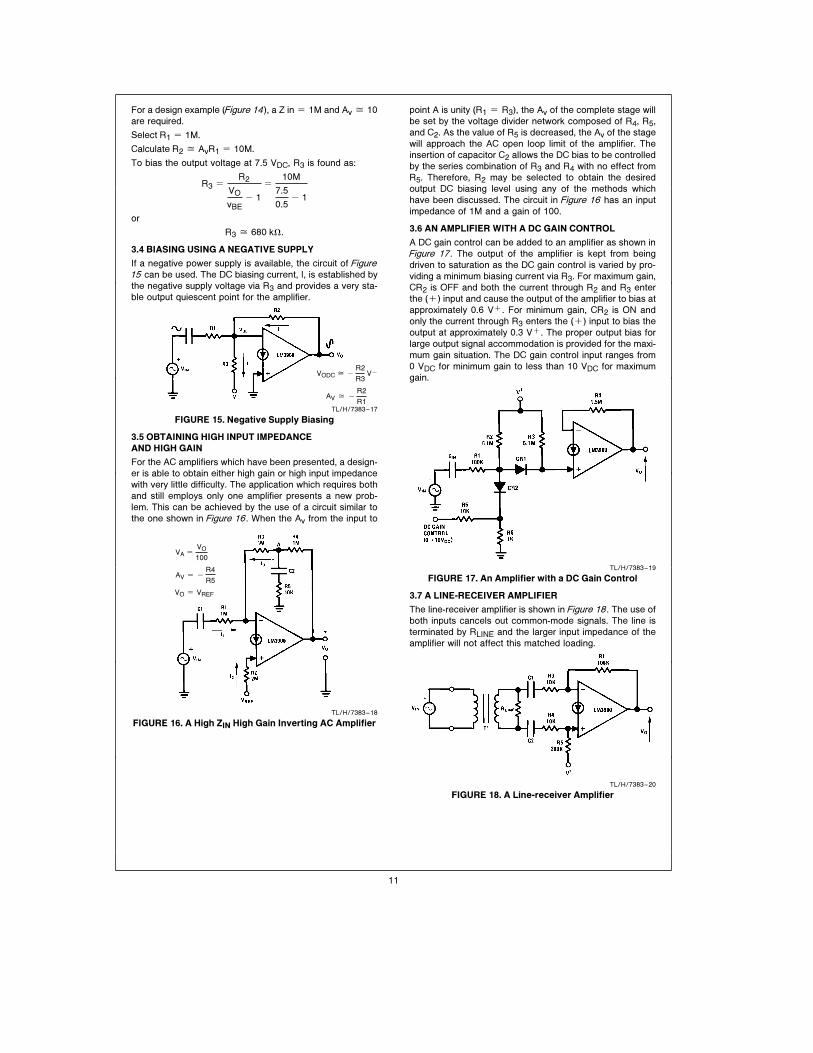
3.4 BIASING USING A NEGATIVE SUPPLY
If a negative power supply is available, the circuit of Figure15 can be used. The DC biasing current, I, is established by
the negative supply voltage via R3 and provides a very sta-
ble output quiescent point for the amplifier.
VODC j b
R2
R3Vb
AV j b
R2
R1TL/H/7383–17
FIGURE 15. Negative Supply Biasing
3.5 OBTAINING HIGH INPUT IMPEDANCE
AND HIGH GAIN
For the AC amplifiers which have been presented, a design-
er is able to obtain either high gain or high input impedance
with very little difficulty. The application which requires both
and still employs only one amplifier presents a new prob-
lem. This can be achieved by the use of a circuit similar to
the one shown in Figure 16. When the Av from the input to
VA e
VO
100
AV e b
R4
R5
VO e VREF
TL/H/7383–18
FIGURE 16. A High ZIN High Gain Inverting AC Amplifier
point A is unity (R1 e R3), the Av of the complete stage will
be set by the voltage divider network composed of R4, R5,
and C2. As the value of R5 is decreased, the Av of the stage
will approach the AC open loop limit of the amplifier. The
insertion of capacitor C2 allows the DC bias to be controlled
by the series combination of R3 and R4 with no effect from
R5. Therefore, R2 may be selected to obtain the desired
output DC biasing level using any of the methods which
have been discussed. The circuit in Figure 16 has an input
impedance of 1M and a gain of 100.
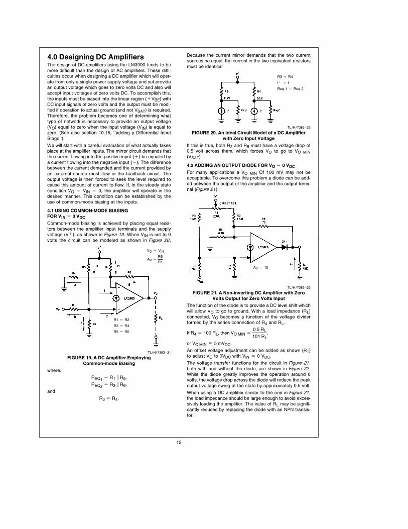
3.6 AN AMPLIFIER WITH A DC GAIN CONTROL
A DC gain control can be added to an amplifier as shown in
Figure 17. The output of the amplifier is kept from being
driven to saturation as the DC gain control is varied by pro-
viding a minimum biasing current via R3. For maximum gain,
CR2 is OFF and both the current through R2 and R3 enter
the (a) input and cause the output of the amplifier to bias at
approximately 0.6 Va. For minimum gain, CR2 is ON and
only the current through R3 enters the (a) input to bias the
output at approximately 0.3 Va. The proper output bias for
large output signal accommodation is provided for the maxi-
mum gain situation. The DC gain control input ranges from
0 VDC for minimum gain to less than 10 VDC for maximum
gain.
TL/H/7383–19
FIGURE 17. An Amplifier with a DC Gain Control
3.7 A LINE-RECEIVER AMPLIFIER
The line-receiver amplifier is shown in Figure 18. The use of
both inputs cancels out common-mode signals. The line is
terminated by RLINE and the larger input impedance of the
amplifier will not affect this matched loading.
TL/H/7383–20
FIGURE 18. A Line-receiver Amplifier
11
4.0 Designing DC AmplifiersThe design of DC amplifiers using the LM3900 tends to be
more difficult than the design of AC amplifiers. These diffi-
culties occur when designing a DC amplifier which will oper-
ate from only a single power supply voltage and yet provide
an output voltage which goes to zero volts DC and also will
accept input voltages of zero volts DC. To accomplish this,
the inputs must be biased into the linear region (aVBE) with
DC input signals of zero volts and the output must be modi-
fied if operation to actual ground (and not VSAT) is required.
Therefore, the problem becomes one of determining what
type of network is necessary to provide an output voltage
(VO) equal to zero when the input voltage (VIN) is equal to
zero. (See also section 10.15, ‘‘adding a Differential Input
Stage’’).
We will start with a careful evaluation of what actually takes
place at the amplifier inputs. The mirror circuit demands that
the current flowing into the positive input (a) be equaled by
a current flowing into the negative input (b). The difference
between the current demanded and the current provided by
an external source must flow in the feedback circuit. The
output voltage is then forced to seek the level required to
cause this amount of current to flow. If, in the steady state
condition VO e VIN e 0, the amplifier will operate in the
desired manner. This condition can be established by the
use of common-mode biasing at the inputs.
4.1 USING COMMON-MODE BIASING
FOR VIN e 0 VDC
Common-mode biasing is achieved by placing equal resis-
tors between the amplifier input terminals and the supply
voltage (Va), as shown in Figure 19. When VIN is set to 0
volts the circuit can be modeled as shown in Figure 20,
VO j VIN
AV e
R6
R1
R1 e R2
R3 e R4
R5 e R6
TL/H/7383–21
FIGURE 19. A DC Amplifier Employing
Common-mode Biasing
where:
REQ1e R1 ll R5,
REQ2e R2 ll R6,
and
R3 e R4.
Because the current mirror demands that the two current
sources be equal, the current in the two equivalent resistors
must be identical.
R3 e R4
Ia e Ib
Req 1 e Req 2
TL/H/7383–22
FIGURE 20. An Ideal Circuit Model of a DC Amplifier
with Zero Input Voltage
If this is true, both R2 and R6 must have a voltage drop of
0.5 volt across them, which forces VO to go to VO MIN(VSAT).
4.2 ADDING AN OUTPUT DIODE FOR VO e 0 VDC
For many applications a VO MIN Of 100 mV may not be
acceptable. To overcome this problem a diode can be add-
ed between the output of the amplifier and the output termi-
nal (Figure 21).
AV e 10
TL/H/7383–23
FIGURE 21. A Non-inverting DC Amplifier with Zero
Volts Output for Zero Volts Input
The function of the diode is to provide a DC level shift which
will allow VO to go to ground. With a load impedance (RL)
connected, VO becomes a function of the voltage divider
formed by the series connection of R4 and RL.
If R4 e 100 RL, then VO MIN e
0.5 RL
101 RL,
or VO MIN j 5 mVDC.
An offset voltage adjustment can be added as shown (R1)
to adjust VO to 0VDC with VIN e 0 VDC.
The voltage transfer functions for the circuit in Figure 21,
both with and without the diode, are shown in Figure 22.
While the diode greatly improves the operation around 0
volts, the voltage drop across the diode will reduce the peak
output voltage swing of the state by approximately 0.5 volt.
When using a DC amplifier similar to the one in Figure 21,
the load impedance should be large enough to avoid exces-
sively loading the amplifier. The value of RL may be signifi-
cantly reduced by replacing the diode with an NPN transis-
tor.
12
TL/H/7383–24
FIGURE 22. Voltage Transfer Function for a DC
Amplifier with a Voltage Gain of 10
4.3 A DC COUPLED POWER AMPLIFIER (IL s 3 AMPS)
The LM3900 may be used as a power amplifier by the addi-
tion of a Darlington pair at the output. The circuit shown in
Figure 23 can deliver in excess of 3 amps to the load when
the transistors are properly mounted on heat sinks.
TL/H/7383–25
FIGURE 23. A DC Power Amplifier
4.4 GROUND REFERENCING A DIFFERENTIAL
VOLTAGE
The circuit in Figure 24 employs the LM3900 to ground ref-
erence a DC differential input voltage. Current I1 is larger
TL/H/7383–26
FIGURE 24. Ground Referencing a Differential
Input DC Voltage
than current I3 by a factor proportional to the differential
voltage, VR. The currents labeled onFigure 24 are given by:
I1 e
V1 a VR b w
R1
I2 e w/R2
I3 e
(V1 b w)
R3
and I4 e
VO b w
R4
where
w A VBE at either input terminal of the LM3900.
Since the input current mirror demands that
Ib e Ia;
and Ia e I1 b I2
and Ib e I3 a I4
Therefore I4 e I1 b I2 b I3.
Substituting in from the above equation
VO b w
R4
e
(V1 a VR b w)
R1
b
(w)
R2
b
(V1 b w)
R3
and as R1 e R2 e R3 e R4
VO e (V1 a VR b w) b (w) b V1 a w a w
or
VO e VR.
The resistors are kept large to minimize loading. With the
10 MX resistors which are shown on the figure, an error
exists at small values of V1 due to the input bias current at
the (–) input. For simplicity this has been neglected in the
circuit description. Smaller R values reduce the percentage
error or the bias current can be supplied by an additional
amplifier (see Section 10.7.1).
For proper operation, the differential input voltage must be
limited to be within the output dynamic voltage range of the
amplifier and the input voltage V2 must be greater than 1
volt. For example; if V2 e 1 volt, the input voltage V1 may
vary over the range of 1 volt to b13 volts when operating
from a 15 volt supply. Common-mode biasing may be added
as shown in Figure 25 to allow both V1 and V2 to be nega-
tive.
VR e V2 b V1
TL/H/7383–27
FIGURE 25. A Network to Invert and to Ground
Reference a Negative DC Differential Input Voltage
4.5 A UNITY GAIN BUFFER AMPLIFIER
The buffer amplifier with a gain of one is the simplest DC
application for the LM3900. The voltage applied to the input
(Figure 26) will be reproduced at the output. However, the
input voltage must be greater than one VBE but less than
the maximum output swing. Common-mode biasing can be
added to extend VIN to 0 VDC, if desired.
13

VIN l VBE
TL/H/7383–28
FIGURE 26. A Unity-gain DC Buffer Amplifier
5.0 Designing Voltage RegulatorsMany voltage regulators can be designed which make use
of the basic amplifier of the LM3900. The simplest is shown
in Figure 27a where only a Zener diode and a resistor are
added. The voltage at the (–) input (one VBE j 0.5 VDC)
appears across R and therefore a resistor value of 510X will
cause approximately 1 mA of bias current to be drawn
through the Zener. This biasing is used to reduce the noise
output of the Zener as the 30 nA input current is too small
for proper Zener biasing. To compensate for a positive tem-
perature coefficient of the Zener, an additional resistor can
be added, R2, (Figure 27b) to introduce an arbitrary number,
N, of ‘‘effective’’ VBE drops into the expression for the out-
put voltage. The negative temperature coefficient of these
diodes will also be added to temperature compensate the
DC output voltage. For a larger output current, an emitter
follower (Q1 of Figure 27c) can be added. This will multiply
the 10 mA (max.) output current of the LM3900 by the b of
the added transistor. For example, a b e 30 will provide a
max. load current of 300 mA. This added transistor also
reduces the output impedance. An output frequency com-
pensation capacitor is generally not required but may be
added, if desired, to reduce the output impedance at high
frequencies.
The DC output voltage can be increased and still preserve
the temperature compensation of Figure 27b by adding re-
sistors RA and RB as shown in Figure 27d. This also can be
accomplished without the added transistor, Q1. The unregu-
lated input voltage, which is applied to pin 14 of the LM3900
(and to the collector of Q1, if used) must always exceed the
regulated DC output voltage by approximately 1V, when the
unit is not current boosted or approximately 2V when the
NPN current boosting transistor is added.
5.1 REDUCING THE INPUT-OUTPUT VOLTAGE
The use of an external PNP transistor will reduce the re-
quired (VIN b VOUT) to a few tenths of a volt. This will
depend on the saturation characteristics of the external
transistor at the operating current level. The circuit, shown
in Figure 28, uses the LM3900 to supply base drive to the
PNP transistor. The resistors R1 and R2 are used to allow
the output of the amplifier to turn OFF the PNP transistor. It
is important that pin 14 of the LM3900 be tied to the aVINline to allow this OFF control to properly operate. Larger
voltages are permissible (if the base-emitter junction of Q1is prevented from entering a breakdown by a shunting di-
ode, for example), but smaller voltages will not allow the
output of the amplifier to raise enough to give the OFF con-
trol.
The resistor, R3, is used to supply the required bias current
for the amplifier and R4 is again used to bias the Zener
diode. Due to a larger gain, a compensation capacitor, CO,
is required. Temperature compensation could be added as
was shown in Figure 27b.
VO e VZ a w
TL/H/7383–29
(a) Basic Current
VO e VZ a Nw
TL/H/7383–30
(b) Temperature Compensating
VO e VZ a w
TL/H/7383–31
(c) Current Boosting
TL/H/7383–32
(d) Raising VO Without Disturbing Temperature Compensation
FIGURE 27. Simple Voltage Regulators
14
TL/H/7383–33
FIGURE 28. Reducing (VIN b VOUT)
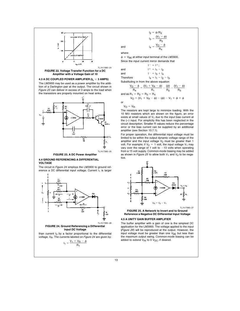
5.2 PROVIDING HIGH INPUT VOLTAGE PROTECTION
One of the four amplifiers can be used to regulate the sup-
ply line for the complete package (pin 14), to provide protec-
tion against large input voltage conditions, and in addition,
to supply current to an external load. This circuit is shown in
Figure 29. The regulated output voltage is the sum of the
Zener voltage, CR2, and the VBE of the inverting input termi-
nal. Again, temperature compensation can be added as in
Figure 27b. The second Zener, CR1, is a low tolerance com-
ponent which simply serves as a DC level shift to allow the
output voltage of the amplifier to control the conduction of
the external transistor, Q1. This Zener voltage should be
approximately one-half of the CR2 voltage to position the
DC Output voltage level of the amplifier approximately in the
center of the dynamic range.
TL/H/7383–34
FIGURE 29. High VIN Protection and Self-regulation
The base drive current for Q1 is supplied via R1. The maxi-
mum current through R1 should be limited to 10 mA as
IMAX e
VIN (MAX) b (VO a VBE)
R1
To increase the maximum allowed input voltage, reduce the
output ripple, or to reduce the (VIN b VOUT) requirements of
this circuit, the connection described in the next section is
recommended.
5.3 HIGH INPUT VOLTAGE PROTECTION AND LOW (VINb VOUT)
The circuit shown in Figure 30 basically adds one additional
transistor to the circuit of Figure 29 to improve the perform-
ance. In this circuit both transistors (Q1 and Q2) absorb any
high input voltages (and therefore need to be high voltage
devices) without any increases in current (as with R1 of Fig-ure 29). The resistor R1 (of Figure 30) provides a ‘‘start-up’’
current into the base of Q2.
A new input connection is shown on this regulator (the type
on Figure 29 could also be used) to control the DC output
voltage. The Zener is biased via R4 (at approximately 1 mA).
The resistors R3 and R6 provide gain (non-inverting) to al-
low establishing VO at any desired voltage larger than VZ.
Temperature compensation of either sign (gTC) can be ob-
tained by shunting a resistor from either the (a) input to
ground (to add a TC to VO) or from the (b) input to ground
(to add bTC to VO). To understand this, notice that the
resistor, R, from the (a) input to ground will add bN VBE to
VO where
N e 1 a
R3
R,
and VBE is the base emitter voltage of the transistor at the
(a) input. This then also adds a positive temperature
change at the output to provide the desired temperature
correction.
The added transistor, Q2, also increases the gain (which
reduces the output impedance) and if a power device is
used for Q1 large load currents (amps) can be supplied. This
regulator also supplies the power to the other three amplifi-
ers of the LM3900.
5.4 REDUCING INPUT VOLTAGE DEPENDENCE AND
ADDING SHORT-CIRCUIT PROTECTION
To reduce ripple feedthrough and input voltage depen-
dence, diodes can be added as shown in Figure 31 to drop-
out the start once start-up has been achieved. Short-circuit
protection can also be added as shown in Figure 32.
The emitter resistor of Q2 will limit the maximum current of
Q2 to (VO b 2 VBE)/R5.
TL/H/7383–35
FIGURE 30. A High VIN Protected, Low (VIN b VOUT) Regulator
15
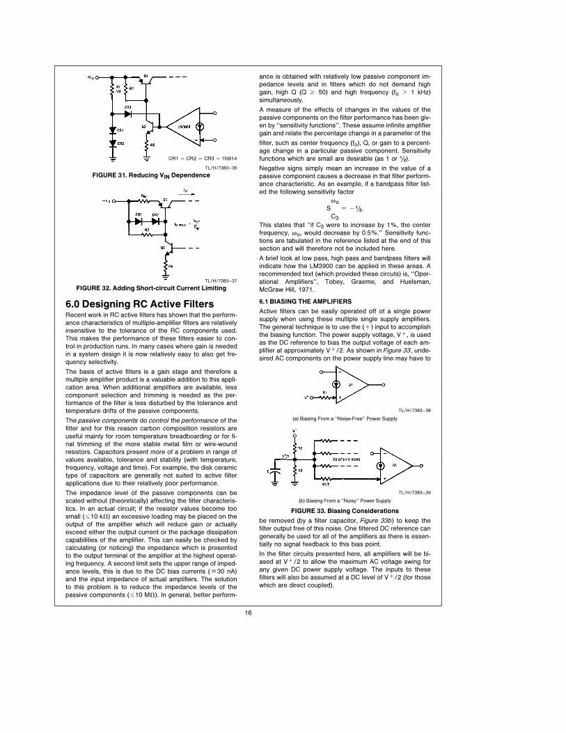
CR1 e CR2 e CR3 e 1N914
TL/H/7383–36
FIGURE 31. Reducing VIN Dependence
TL/H/7383–37
FIGURE 32. Adding Short-circuit Current Limiting
6.0 Designing RC Active FiltersRecent work in RC active filters has shown that the perform-
ance characteristics of multiple-amplifier filters are relatively
insensitive to the tolerance of the RC components used.
This makes the performance of these filters easier to con-
trol in production runs. In many cases where gain is needed
in a system design it is now relatively easy to also get fre-
quency selectivity.
The basis of active filters is a gain stage and therefore a
multiple amplifier product is a valuable addition to this appli-
cation area. When additional amplifiers are available, less
component selection and trimming is needed as the per-
formance of the filter is less disturbed by the tolerance and
temperature drifts of the passive components.
The passive components do control the performance of the
filter and for this reason carbon composition resistors are
useful mainly for room temperature breadboarding or for fi-
nal trimming of the more stable metal film or wire-wound
resistors. Capacitors present more of a problem in range of
values available, tolerance and stability (with temperature,
frequency, voltage and time). For example, the disk ceramic
type of capacitors are generally not suited to active filter
applications due to their relatively poor performance.
The impedance level of the passive components can be
scaled without (theoretically) affecting the filter characteris-
tics. In an actual circuit; if the resistor values become too
small (s10 kX) an excessive loading may be placed on the
output of the amplifier which will reduce gain or actually
exceed either the output current or the package dissipation
capabilities of the amplifier. This can easily be checked by
calculating (or noticing) the impedance which is presented
to the output terminal of the amplifier at the highest operat-
ing frequency. A second limit sets the upper range of imped-
ance levels, this is due to the DC bias currents (j30 nA)
and the input impedance of actual amplifiers. The solution
to this problem is to reduce the impedance levels of the
passive components (s10 MX). In general, better perform-
ance is obtained with relatively low passive component im-
pedance levels and in filters which do not demand high
gain, high Q (Q t 50) and high frequency (fo l 1 kHz)
simultaneously.
A measure of the effects of changes in the values of the
passive components on the filter performance has been giv-
en by ‘‘sensitivity functions’’. These assume infinite amplifier
gain and relate the percentage change in a parameter of the
filter, such as center frequency (fo), Q, or gain to a percent-
age change in a particular passive component. Sensitivity
functions which are small are desirable (as 1 or (/2).
Negative signs simply mean an increase in the value of a
passive component causes a decrease in that filter perform-
ance characteristic. As an example, if a bandpass filter list-
ed the following sensitivity factor
S
0o
C3
e b(/2.
This states that ‘‘if C3 were to increase by 1%, the center
frequency, 0o, would decrease by 0.5%.’’ Sensitivity func-
tions are tabulated in the reference listed at the end of this
section and will therefore not be included here.
A brief look at low pass, high pass and bandpass filters will
indicate how the LM3900 can be applied in these areas. A
recommended text (which provided these circuts) is, ‘‘Oper-
ational Amplifiers’’, Tobey, Graeme, and Huelsman,
McGraw Hill, 1971.
6.1 BIASING THE AMPLIFIERS
Active filters can be easily operated off of a single power
supply when using these multiple single supply amplifiers.
The general technique is to use the (a) input to accomplish
the biasing function. The power supply voltage, Va, is used
as the DC reference to bias the output voltage of each am-
plifier at approximately Va/2. As shown in Figure 33, unde-
sired AC components on the power supply line may have to
TL/H/7383–38
(a) Biasing From a ‘‘Noise-Free’’ Power Supply
TL/H/7383–39
(b) Biasing From a ‘‘Noisy’’ Power Supply
FIGURE 33. Biasing Considerations
be removed (by a filter capacitor, Figure 33b) to keep the
filter output free of this noise. One filtered DC reference can
generally be used for all of the amplifiers as there is essen-
tially no signal feedback to this bias point.
In the filter circuits presented here, all amplifiers will be bi-
ased at Va/2 to allow the maximum AC voltage swing for
any given DC power supply voltage. The inputs to these
filters will also be assumed at a DC level of Va/2 (for those
which are direct coupled).
16

6.2 A HIGH PASS ACTIVE FILTER
A single amplifier high pass RC active filter is shown in Fig-ure 34. This circuit is easily biased using the (a) input of the
LM3900. The resistor, R3, can be simply made equal to R2and a bias reference of Va/2 will establish the output Q
point at this value (Va/2). The input is capacitively coupled
(C1) and there are therefore no further DC biasing problems.
fc e 1 kHz
TL/H/7383–40
FIGURE 34. A High Pass Active Filter
The design procedure for this filter is to select the pass
band gain, HO, the Q and the corner frequency, fc. A Q
value of 1 gives only a slight peaking near the bandedge
(k2 dB) and smaller Q values decrease this peaking. The
slope of the skirt of this filter is 12 dB/octave (or 40 dB/dec-
ade). If the gain, HO, is unity all capacitors have the same
value. The design proceeds as:
Given: HO, Q and 0c e 2qfc
To find: R1, R2, C1, C2, and C3
let C1 e C3 and choose a convenient starting value.
Then:
R1 e
1
Q 0cC1 (2HO a 1)(1)
R2 e
Q
0cC1(2 HO a 1), (2)
and
C2 e
C1
HO. (3)
As a design example,
Require: HO e 1,
Q e 10,
and fc e 1 kHz (0c e 6.28 c 103 rps).
Start by selecting C1 e 300 pF and then from equation (1)
R1 e
1
(10) (6.28 c 103) (3 c 10b10) (3)
R1 e 17.7 kX
and from equation (2)
R2 e
10 (3)
(6.28 c 103) (3 c 10b10)
R2 e 15.9 MX
and from equation (3)
C2 e
C1
1e C1
Now we see that the value of R2 is quite large; but the other
components look acceptable. Here is where impedance
scaling comes in. We can reduce R2 to the more convenient
value of 10 MX which is a factor of 1.59:1. Reducing R1 by
this same scaling factor gives:
R1NEWe
17.7 c 103
1.59e 11.1 kX
and the capacitors are similarly reduced in impedance as:#C1 e C2 e C3JNEW e (1.59) (300) pF
C1NEWe 477 pF.
To complete the design, R3 is made equal to R2 (10 MX)
and a VREF of Va/2 is used to bias the output for large
signal accommodation.
Capacitor values should be adjusted to use standard valued
components by using impedance scaling as a wider range
of standard resistor values is generally available.
6.3 A LOW PASS ACTIVE FILTER
A single amplifier low pass filter is shown in Figure 35. The
resistor, R4, is used to set the output bias level and is se-
lected after the other resistors have been established.
GAIN e 1
fc e 1 kHz
TL/H/7383–41
FIGURE 35. A Low Pass Active Filter
The design procedure is as follows:
Given: HO, Q, and 0c e 2qfc
To find: R1, R2, R3, R4, C1, and C2
Let C1 be a convenient value,
then
C2 e KC1 (4)
where K is a constant which can be used to adjust compo-
nent values. For example, with K e 1, C1 e C2. Larger
values of K can be used to reduce R2 and R3 at the ex-
pense of a larger value for C2.
R1 e
R2
HO, (5)
R2 e
1
2Q 0C C1 Ð1 g 01 a
4Q2 (HO a 1)
K ( (6)
and
R3 e
1
0c2C1
2R2(K) (7)
As a design example:
Require: HO e 1,
Q e 1,
and fc e 1 kHz (0c e 6.28 c 103 rps).
17
Start by selecting C1 e 300 pF and K e 1 so C2 is also 300
pF (equation 4).
Now from equation (6)
R2 e
1
2 (1) (6.28 c 103) (3 c 10b10) Ð1 g 01 a4 (2) (R2 e 1.06 MX
Then from equation (5)
R1 e R2 e 1.06 MX
and finally from equation (7)
R3 e
1
(6.28 c 103)2 (3 c 10b10)2 (1.06 c 106) (1)
R3 e 266 kX.
To select R4, we assume the DC input level is 7 VDC and
the DC output of this filter is to also be 7 VDC. This gives us
the circuit ofFigure 36. Notice that HO e 1 gives us not only
TL/H/7383–42
FIGURE 36. Biasing the Low Pass Filter
equal resistor values (R1 and R2) but simplifies the DC bias
calculation as I1 e I2 and we have a DC amplifier with a
gain of b1 (so if the DC input voltage increases 1 VDC the
output voltage decreases 1 VDC). The resistors R1 and R2are in parallel so that the circuit simplifies to that shown in
Figure 37 where the actual resistance values have been
added. The resistor R4 is given by
R4 e 2#R1
2a R3J a R3
or, using values
R4 e 2 #1 MX
2a 266kJ j 1.5 MX
R1 ll R2 e R1/2
TL/H/7383–43
FIGURE 37. Biasing Equivalent Circuit
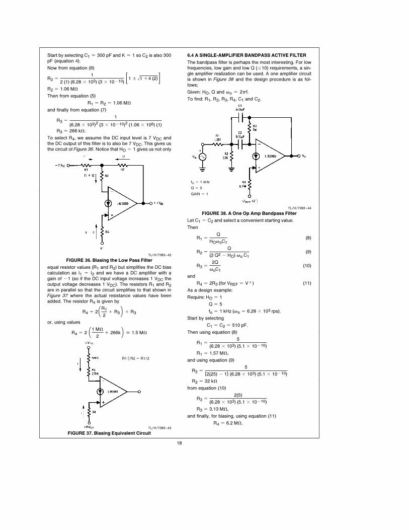
6.4 A SINGLE-AMPLIFIER BANDPASS ACTIVE FILTER
The bandpass filter is perhaps the most interesting. For low
frequencies, low gain and low Q (s10) requirements, a sin-
gle amplifier realization can be used. A one amplifier circuit
is shown in Figure 38 and the design procedure is as fol-
lows;
Given: HO, Q and 0o e 2qf.
To find: R1, R2, R3, R4, C1 and C2.
fo e 1 kHz
Q e 5
GAIN e 1
TL/H/7383–44
FIGURE 38. A One Op Amp Bandpass Filter
Let C1 e C2 and select a convenient starting value.
Then
R1 e
Q
HO0oC1(8)
R2 e
Q
(2 Q2 b HO) 0o C1(9)
R3 e
2Q
0oC1(10)
and
R4 e 2R3 (for VREF e Va) (11)
As a design example:
Require: HO e 1
Q e 5
fo e 1 kHz (0o e 6.28 c 103 rps).
Start by selecting
C1 e C2 e 510 pF.
Then using equation (8)
R1 e
5
(6.28 c 103) (5.1 c 10b10)
R1 e 1.57 MX,
and using equation (9)
R2 e
5
[2(25) b 1] (6.28 c 103) (5.1 c 10b10)
R2 e 32 kX
from equation (10)
R3 e
2(5)
(6.28 c 103) (5.1 c 10b10)
R3 e 3.13 MX,
and finally, for biasing, using equation (11)
R4 e 6.2 MX.
18
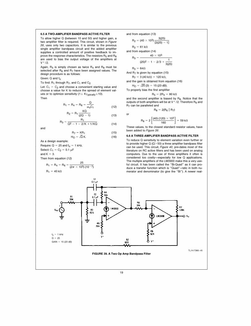
6.5 A TWO-AMPLIFIER BANDPASS ACTIVE FILTER
To allow higher Q (between 10 and 50) and higher gain, a
two amplifier filter is required. This circuit, shown in Figure39, uses only two capacitors. It is similar to the previous
single amplifier bandpass circuit and the added amplifier
supplies a controlled amount of positive feedback to im-
prove the response characteristics. The resistors R5 and R8are used to bias the output voltage of the amplifiers at
Va/2.
Again, R5 is simply chosen as twice R4 and R8 must be
selected after R6 and R7 have been assigned values. The
design procedure is as follows:
Given: Q and fo
To find: R1 through R7, and C1 and C2
Let: C1 e C2 and choose a convenient starting value and
choose a value for K to reduce the spread of element val-
ues or to optimize sensitivity (1s KTypicallys10).
Then
R1 e R4 e R6 e
Q
0oC1 (12)
R2 e R1KQ
(2Q b 1) (13)
R3 e
R1
Q2 b 1 b 2/K a1/KQ (14)
and
R7 e KR1 (15)
HO e 0Q K. (16)
As a design example:
Require: Q e 25 and fo e 1 kHz.
Select: C1 e C2 e 0.1 mF
and K e 3.
Then from equation (12)
R1 e R4 e R6 e
25
(2q c 103) (10b7)
R1 e 40 kX
and from equation (13)
R2 e (40 c 103)3(25)
[2(25) b 1]
R2 e 61 kX
and from equation (14)
R3 e
40 c 103
(25)2 b 1 b 2/3 a
1
3(25)
R3 e 64X
And R7 is given by equation (15)
R7 e 3 (40 kX) e 120 kX,
and the gain is obtained from equation (16)
HO e 025 (3) e 15 (23 dB).
To properly bias the first amplifier
R5 e 2R4 e 80 kX
and the second amplifier is biased by R8. Notice that the
outputs of both amplifiers will be at Va/2. Therefore R6 and
R7 can be paralleled and
R8 e 2(R6 ll R7)
or
R8 e 2 Ð (40) (120) c 103
160 ( e 59 kX
These values, to the closest standard resistor values, have
been added to Figure 39.
6.6 A THREE-AMPLIFIER BANDPASS ACTIVE FILTER
To reduce Q sensitivity to element variation even further or
to provide higher Q (Ql50) a three amplifier bandpass filter
can be used. This circuit, Figure 40, pre-dates most of the
literature on RC active filters and has been used on analog
computers. Due to the use of three amplifiers it often is
considered too costlyÐespecially for low Q applications.
The multiple amplifiers of the LM3900 make this a very use-
ful circuit. It has been called the ‘‘Bi-Quad’’ as it can pro-
duce a transfer function which is ‘‘Quad’’–ratic in both nu-
merator and denominator (to give the ‘‘Bi’’). A newer real-
fo e 1 kHz
Q e 25
GAIN e 15 (23 dB)
TL/H/7383–45
FIGURE 39. A Two Op Amp Bandpass Filter
19
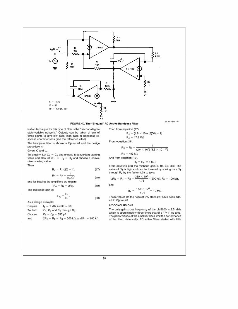
fo e 1 kHz
Q e 50
HO e 100 (40 dB)
TL/H/7383–46FIGURE 40. The ‘‘Bi-quad’’ RC Active Bandpass Filter
ization technique for this type of filter is the ‘‘second-degree
state-variable network.’’ Outputs can be taken at any of
three points to give low pass, high pass or bandpass re-
sponse characteristics (see the reference cited).
The bandpass filter is shown in Figure 40 and the design
procedure is:
Given: Q and fo.
To simplify: Let C1 e C2 and choose a convenient starting
value and also let 2R1 e R2 e R3 and choose a conve-
nient starting value.
Then:
R4 e R1 (2Q b 1), (17)
R5 e R7 e
1
0o C1,
(18)
and for biasing the amplifiers we require
R6 e R8 e 2R5. (19)
The mid-band gain is:
HO e
R4
R1.
(20)
As a design example;
Require: fo e 1 kHz and Q e 50.
To find: C1, C2 and R1 through R8.
Choose: C1 e C2 e 330 pF
and 2R1 e R2 e R3 e 360 kX, and R1 e 180 kX.
Then from equation (17),
R4 e (1.8 c 105) [2(50) b 1]
R4 e 17.8 MX
From equation (18),
R5 e R7 e
1
(2q c 103) (3.3 c 10b10)
R5 e 483 kX.
And from equation (19),
R6 e R8 j 1 MX.
From equation (20) the midband gain is 100 (40 dB). The
value of R4 is high and can be lowered by scaling only R1through R4 by the factor 1.78 to give:
2R1 e R2 e R3 e
360 c 103
1.78e 200 kX, R1 e 100 kX.
and
R4 e
17.8 c 106
1.78e 10 MX.
These values (to the nearest 5% standard) have been add-
ed to Figure 40.
6.7 CONCLUSIONS
The unity-gain cross frequency of the LM3900 is 2.5 MHz
which is approximately three times that of a ‘‘741’’ op amp.
The performance of the amplifier does limit the performance
of the filter. Historically, RC active filters started with little
20
concern for these practical problems. The sensitivity func-
tions were a big step forward as these demonstrated that
many of the earlier suggested realization techniques for RC
active filters had passive component sensitivity functions
which varied as Q or even Q2. The Bi-Quad circuit has re-
duced the problems with the passive components (sensitivi-
ty functions of 1 or (/2) and recently the contributions of the
amplifier on the performance of the filter are being investi-
gated. An excellent treatment (‘‘The Biquad: Part I Ð Some
Practical Design Considerations,‘‘ L.C. Thomas, IEEE
Transactions on Circuit Theory, Vol. CT-18, No. 3, May
1971) has indicated the limits imposed by the characteris-
tics of the amplifier by showing that the design value of Q
(QD) will differ from the actual measured value of Q (QA) by
the given relationship
QA e
QD
1 a
2QD
AO0a(0a b 20p)
(21)
where AO is the open loop gain of the amplifier, 0a is the
dominant pole of the amplifier and 0p is the resonant fre-
quency of the filter. The result is that the trade-off between
Q and center frequency (0p) can be determined for a given
set of amplifier characteristics. When QA differs significantly
from QD excessive dependence on amplifier characteristics
is indicated. An estimate of the limitations of an amplifier
can be made by arbitrarily allowing approximately a 10%
effect on QA which results if
2QD
AO0a(0a b 20p) e 0.1
or #0p
0a J e 2.5 c 10b2 #AO
QDJ a 0.5. (22)
As an example, using AO e 2800 for the LM3900 we can
estimate the maximum frequency where a QD e 50 would
be reasonable as
fp
fae 2.5 c 10b2 #2.8 c 103
5 c10 J a 0.5
or
fp
fae 1.9
therefore
fp e 1.9 fa.
Again, using data of the LM3900, fa e 1 kHz so this upper
frequency limit is approximately 2 kHz for the assumed Q of
50. As indicated in equation (26) the value of QA can actual-
ly exceed the value of QD (Q enhancement) and, as expect-
ed, the filter can even provide its own input (oscillating).
Excess phase shift in the high frequency characteristics of
the amplifier typically cause unexpected oscillations. Phase
compensation can be used in the Bi-Quad network to re-
duce this problem (see L.C. Thomas paper).
Designing for large passband gain also increases filter de-
pendency on the characteristics of the amplifier and finally
signal to noise ratio can usually be improved by taking gain
in an input RC active filter (again see L.C. Thomas paper).
Somewhat larger Q’s can be achieved by adding more filter
sections in either a synchronously tuned cascade (filters
tuned to same center frequency and taking advantage of
the bandwidth shrinkage factor which results from the series
connection) or as a standard multiple pole filter. All of the
conventional filters can be realized and selection is based
upon all of the performance requirements which the applica-
tion demands. The cost advantages of the LM3900, the rel-
atively large bandwidth and the ease of operation on a sin-
gle power supply voltage make this product an excellent
‘‘building block’’ for RC active filters.
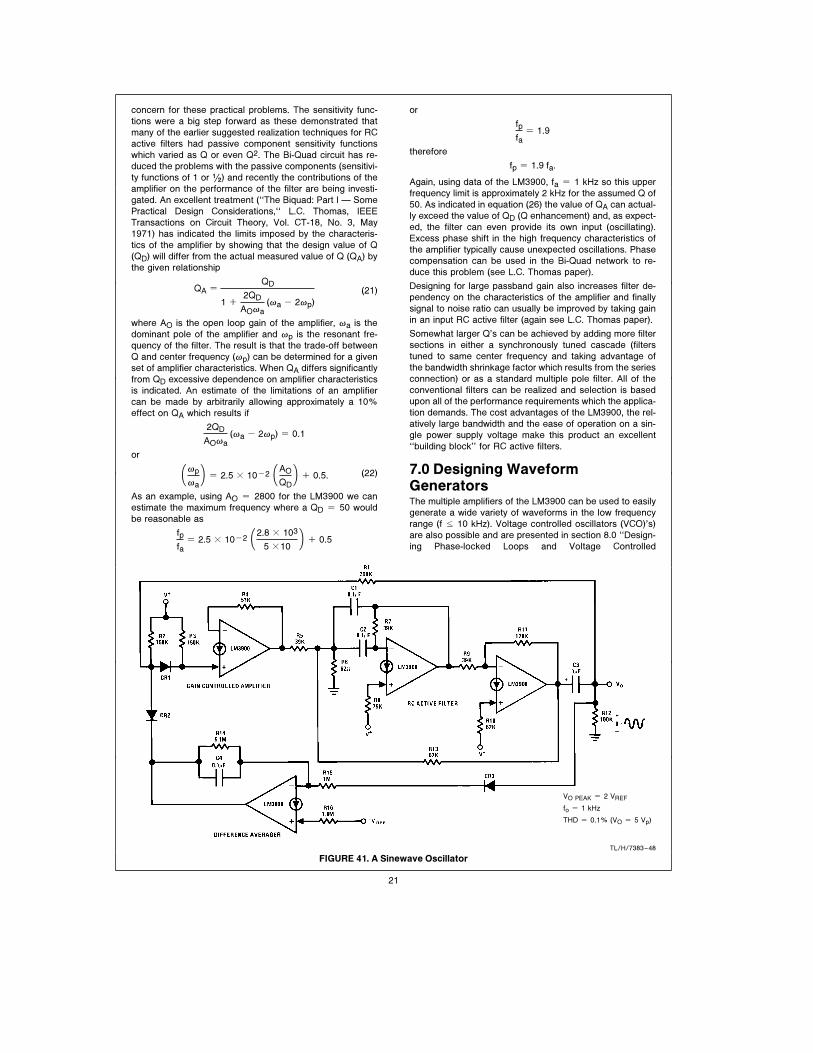
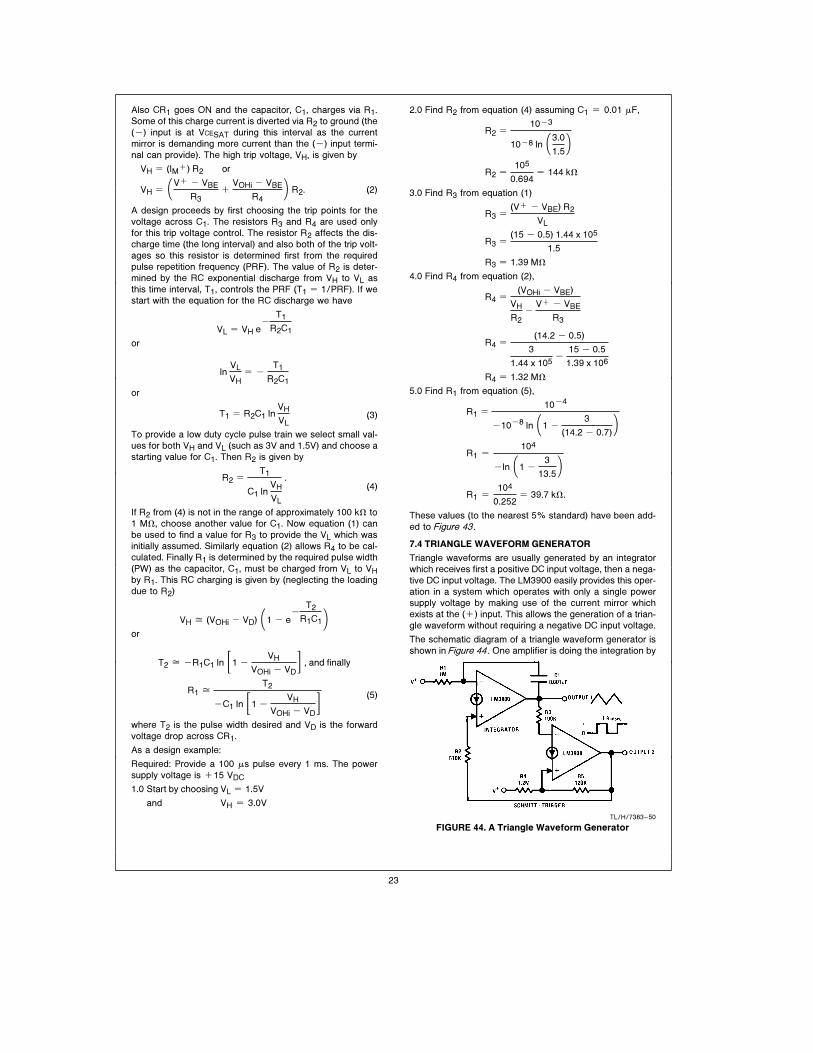
7.0 Designing WaveformGeneratorsThe multiple amplifiers of the LM3900 can be used to easily
generate a wide variety of waveforms in the low frequency
range (f s 10 kHz). Voltage controlled oscillators (VCO)’s)
are also possible and are presented in section 8.0 ‘‘Design-
ing Phase-locked Loops and Voltage Controlled
VO PEAK e 2 VREF
fo e 1 kHz
THD e 0.1% (VO e 5 Vp)
TL/H/7383–48
FIGURE 41. A Sinewave Oscillator
21
Oscillators.’’ In addition, power oscillators (such as noise
makers, etc.) are presented in section 10.11.3. The wave-
form generators which will be presented in this section are
mainly of the switching type, but for completeness a sine-
wave oscillator has been included.
7.1 A SINEWAVE OSCILLATOR
The design of a sinewave oscillator presents problems in
both amplitude stability (and predictability) and output wave-
form purity (THD). If an RC bandpass filter is used as a high
Q resonator for the oscillator circuit we can obtain an output
waveform with low distortion and eliminate the problem of
relative center frequency drift which exists if the active filter
were used simply to filter the output of a separate oscillator.
A sinewave oscillator which is based on this principle is
shown in Figure 41. The two-amplifier RC active filter is
used as it requires only two capacitors and provides an over-
all non-inverting phase characteristic. If we add a non-in-
verting gain controlled amplifier around the filter we obtain
the desired oscillator configuration. Finally, the sinewave
output voltage is sensed and regulated as the average value
is compared to a DC reference voltage, VREF, by use of a
differential averaging circuit. It can be shown that with the
values selected for R15 and R16 (ratio of 0.64/1) that there
is first order temperature compensation for CR3 and the
internal input diodes of the IC amplifier which is used for the
‘‘difference averager’’. Further, this also provides a simple
way to regulate and to predict the magnitude of the output
sinewave as
VO peak e 2 VREF
which is essentially independent of both temperature and
the magnitude of the power supply voltage (if VREF is de-
rived from a stable voltage source).
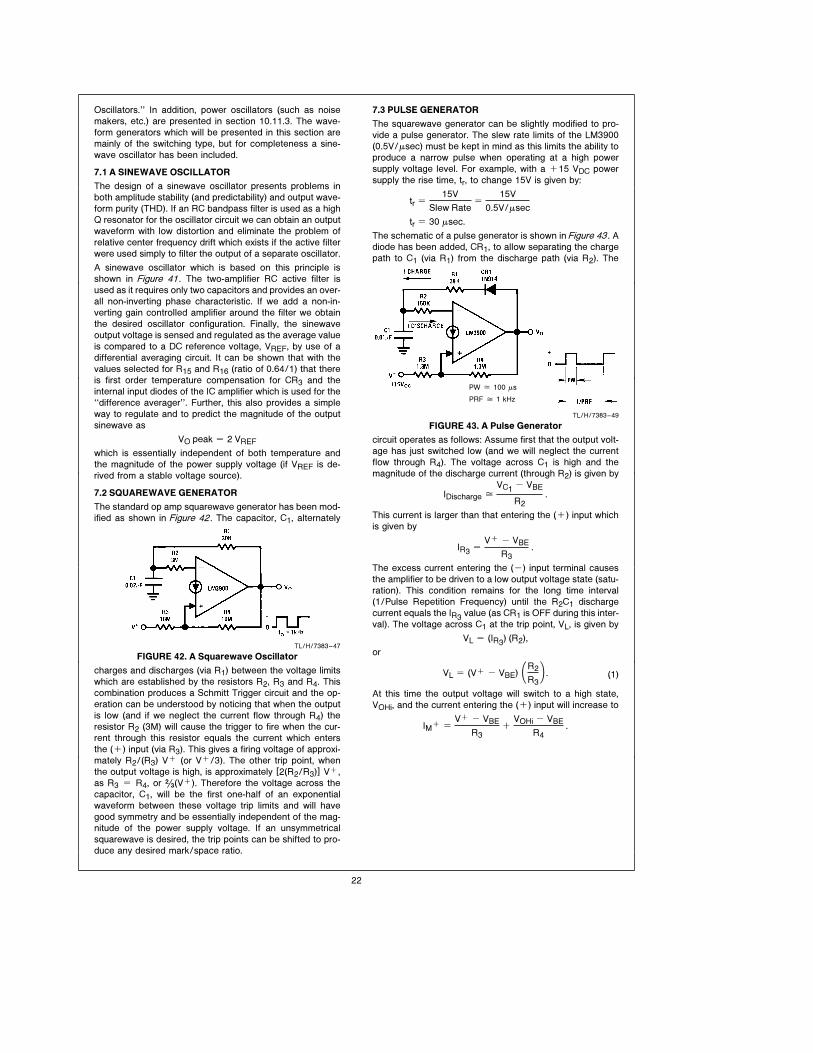
7.2 SQUAREWAVE GENERATOR
The standard op amp squarewave generator has been mod-
ified as shown in Figure 42. The capacitor, C1, alternately
TL/H/7383–47
FIGURE 42. A Squarewave Oscillator
charges and discharges (via R1) between the voltage limits
which are established by the resistors R2, R3 and R4. This
combination produces a Schmitt Trigger circuit and the op-
eration can be understood by noticing that when the output
is low (and if we neglect the current flow through R4) the
resistor R2 (3M) will cause the trigger to fire when the cur-
rent through this resistor equals the current which enters
the (a) input (via R3). This gives a firing voltage of approxi-
mately R2/(R3) Va (or Va/3). The other trip point, when
the output voltage is high, is approximately [2(R2/R3)] Va,
as R3 e R4, or )/3(Va). Therefore the voltage across the
capacitor, C1, will be the first one-half of an exponential
waveform between these voltage trip limits and will have
good symmetry and be essentially independent of the mag-
nitude of the power supply voltage. If an unsymmetrical
squarewave is desired, the trip points can be shifted to pro-
duce any desired mark/space ratio.
7.3 PULSE GENERATOR
The squarewave generator can be slightly modified to pro-
vide a pulse generator. The slew rate limits of the LM3900
(0.5V/msec) must be kept in mind as this limits the ability to
produce a narrow pulse when operating at a high power
supply voltage level. For example, with a a15 VDC power
supply the rise time, tr, to change 15V is given by:
tr e
15V
Slew Ratee
15V
0.5V/msec
tr e 30 msec.
The schematic of a pulse generator is shown inFigure 43. A
diode has been added, CR1, to allow separating the charge
path to C1 (via R1) from the discharge path (via R2). The
PRF j 1 kHz
PW j 100 ms
TL/H/7383–49
FIGURE 43. A Pulse Generator
circuit operates as follows: Assume first that the output volt-
age has just switched low (and we will neglect the current
flow through R4). The voltage across C1 is high and the
magnitude of the discharge current (through R2) is given by
IDischarge j
VC1b VBE
R2.
This current is larger than that entering the (a) input which
is given by
IR3e
Va b VBE
R3.
The excess current entering the (b) input terminal causes
the amplifier to be driven to a low output voltage state (satu-
ration). This condition remains for the long time interval
(1/Pulse Repetition Frequency) until the R2C1 discharge
current equals the IR3value (as CR1 is OFF during this inter-
val). The voltage across C1 at the trip point, VL, is given by
VL e (IR3) (R2),
or
VL e (Va b VBE) #R2
R3J . (1)
At this time the output voltage will switch to a high state,
VOHi, and the current entering the (a) input will increase to
IMa e
Va b VBE
R3
a
VOHi b VBE
R4.
22
Also CR1 goes ON and the capacitor, C1, charges via R1.
Some of this charge current is diverted via R2 to ground (the
(b) input is at VCESAT during this interval as the current
mirror is demanding more current than the (b) input termi-
nal can provide). The high trip voltage, VH, is given by
VH e (IMa) R2 or
VH e #Va b VBE
R3
a
VOHi b VBE
R4 J R2. (2)
A design proceeds by first choosing the trip points for the
voltage across C1. The resistors R3 and R4 are used only
for this trip voltage control. The resistor R2 affects the dis-
charge time (the long interval) and also both of the trip volt-
ages so this resistor is determined first from the required
pulse repetition frequency (PRF). The value of R2 is deter-
mined by the RC exponential discharge from VH to VL as
this time interval, T1, controls the PRF (T1 e 1/PRF). If we
start with the equation for the RC discharge we have
VL e VH eb
T1
R2C1
or
lnVL
VH
e b
T1
R2C1
or
T1 e R2C1 lnVH
VL(3)
To provide a low duty cycle pulse train we select small val-
ues for both VH and VL (such as 3V and 1.5V) and choose a
starting value for C1. Then R2 is given by
R2 e
T1
C1 lnVH
VL
.(4)
If R2 from (4) is not in the range of approximately 100 kX to
1 MX, choose another value for C1. Now equation (1) can
be used to find a value for R3 to provide the VL which was
initially assumed. Similarly equation (2) allows R4 to be cal-
culated. Finally R1 is determined by the required pulse width
(PW) as the capacitor, C1, must be charged from VL to VHby R1. This RC charging is given by (neglecting the loading
due to R2)
VH j (VOHi b VD) #1 b eb
T2
R1C1Jor
T2 j bR1C1 ln Ð1 b
VH
VOHi b VD ( , and finally
R1 jT2
bC1 ln Ð1 b
VH
VOHi b VD ( (5)
where T2 is the pulse width desired and VD is the forward
voltage drop across CR1.
As a design example:
Required: Provide a 100 ms pulse every 1 ms. The power
supply voltage is a15 VDC
1.0 Start by choosing VL e 1.5V
and VH e 3.0V
2.0 Find R2 from equation (4) assuming C1 e 0.01 mF,
R2 e
10b3
10b8 ln #3.0
1.5JR2 e
105
0.694e 144 kX
3.0 Find R3 from equation (1)
R3 e
(Va b VBE) R2
VL
R3 e
(15 b 0.5) 1.44 x 10⁵
1.5
R3 e 1.39 MX
4.0 Find R4 from equation (2),
R4 e
(VOHi b VBE)
VH
R2
b
Va b VBE
R3
R4 e
(14.2 b 0.5)
3
1.44 x 10⁵b
15 b 0.5
1.39 x 10⁶
R4 e 1.32 MX
5.0 Find R1 from equation (5),
R1 e
10b4
b10b8 ln #1 b
3
(14.2 b 0.7)JR1 e
104
bln #1 b
3
13.5JR1 e
104
0.252e 39.7 kX.
These values (to the nearest 5% standard) have been add-
ed to Figure 43.
7.4 TRIANGLE WAVEFORM GENERATOR
Triangle waveforms are usually generated by an integrator
which receives first a positive DC input voltage, then a nega-
tive DC input voltage. The LM3900 easily provides this oper-
ation in a system which operates with only a single power
supply voltage by making use of the current mirror which
exists at the (a) input. This allows the generation of a trian-
gle waveform without requiring a negative DC input voltage.
The schematic diagram of a triangle waveform generator is
shown inFigure 44. One amplifier is doing the integration by
TL/H/7383–50
FIGURE 44. A Triangle Waveform Generator
23
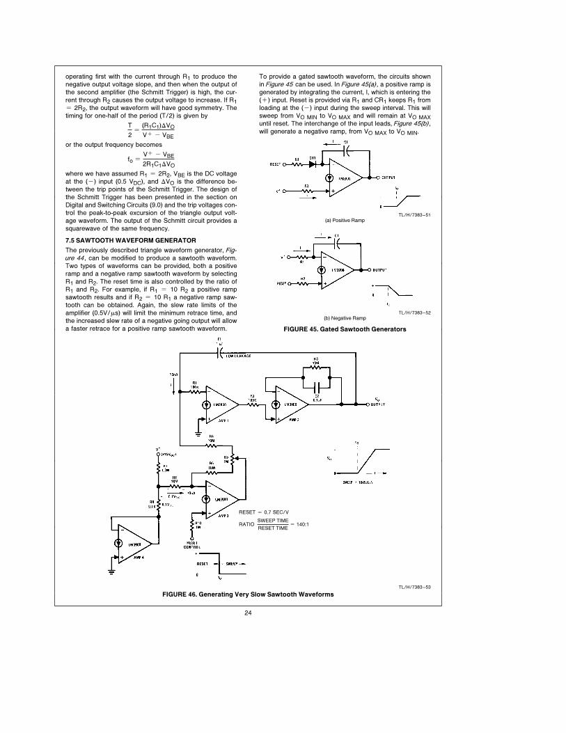
operating first with the current through R1 to produce the
negative output voltage slope, and then when the output of
the second amplifier (the Schmitt Trigger) is high, the cur-
rent through R2 causes the output voltage to increase. If R1e 2R2, the output waveform will have good symmetry. The
timing for one-half of the period (T/2) is given by
T
2e
(R1C1)DVO
Va b VBE
or the output frequency becomes
fo e
Va b VBE
2R1C1DVO
where we have assumed R1 e 2R2, VBE is the DC voltage
at the (b) input (0.5 VDC), and DVO is the difference be-
tween the trip points of the Schmitt Trigger. The design of
the Schmitt Trigger has been presented in the section on
Digital and Switching Circuits (9.0) and the trip voltages con-
trol the peak-to-peak excursion of the triangle output volt-
age waveform. The output of the Schmitt circuit provides a
squarewave of the same frequency.
7.5 SAWTOOTH WAVEFORM GENERATOR
The previously described triangle waveform generator, Fig-ure 44, can be modified to produce a sawtooth waveform.
Two types of waveforms can be provided, both a positive
ramp and a negative ramp sawtooth waveform by selecting
R1 and R2. The reset time is also controlled by the ratio of
R1 and R2. For example, if R1 e 10 R2 a positive ramp
sawtooth results and if R2 e 10 R1 a negative ramp saw-
tooth can be obtained. Again, the slew rate limits of the
amplifier (0.5V/ms) will limit the minimum retrace time, and
the increased slew rate of a negative going output will allow
a faster retrace for a positive ramp sawtooth waveform.
To provide a gated sawtooth waveform, the circuits shown
in Figure 45 can be used. In Figure 45(a) , a positive ramp is
generated by integrating the current, I, which is entering the
(a) input. Reset is provided via R1 and CR1 keeps R1 from
loading at the (b) input during the sweep interval. This will
sweep from VO MIN to VO MAX and will remain at VO MAXuntil reset. The interchange of the input leads, Figure 45(b) ,will generate a negative ramp, from VO MAX to VO MIN.
TL/H/7383–51(a) Positive Ramp
TL/H/7383–52(b) Negative Ramp
FIGURE 45. Gated Sawtooth Generators
RESET e 0.7 SEC/V
RATIOSWEEP TIME
RESET TIMEe 140:1
TL/H/7383–53
FIGURE 46. Generating Very Slow Sawtooth Waveforms
24
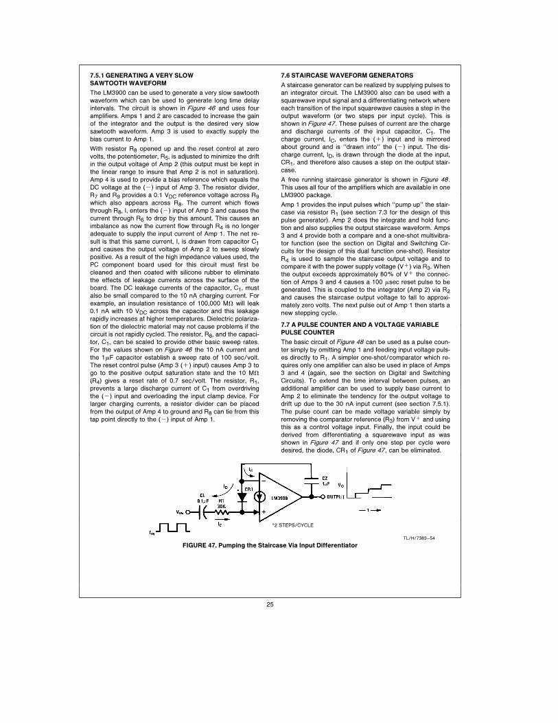
7.5.1 GENERATING A VERY SLOW
SAWTOOTH WAVEFORM
The LM3900 can be used to generate a very slow sawtooth
waveform which can be used to generate long time delay
intervals. The circuit is shown in Figure 46 and uses four
amplifiers. Amps 1 and 2 are cascaded to increase the gain
of the integrator and the output is the desired very slow
sawtooth waveform. Amp 3 is used to exactly supply the
bias current to Amp 1.
With resistor R8 opened up and the reset control at zero
volts, the potentiometer, R5, is adjusted to minimize the drift
in the output voltage of Amp 2 (this output must be kept in
the linear range to insure that Amp 2 is not in saturation).
Amp 4 is used to provide a bias reference which equals the
DC voltage at the (b) input of Amp 3. The resistor divider,
R7 and R9 provides a 0.1 VDC reference voltage across R9which also appears across R8. The current which flows
through R8, I, enters the (b) input of Amp 3 and causes the
current through R6 to drop by this amount. This causes an
imbalance as now the current flow through R4 is no longer
adequate to supply the input current of Amp 1. The net re-
sult is that this same current, I, is drawn from capacitor C1and causes the output voltage of Amp 2 to sweep slowly
positive. As a result of the high impedance values used, the
PC component board used for this circuit must first be
cleaned and then coated with silicone rubber to eliminate
the effects of leakage currents across the surface of the
board. The DC leakage currents of the capacitor, C1, must
also be small compared to the 10 nA charging current. For
example, an insulation resistance of 100,000 MX will leak
0.1 nA with 10 VDC across the capacitor and this leakage
rapidly increases at higher temperatures. Dielectric polariza-
tion of the dielectric material may not cause problems if the
circuit is not rapidly cycled. The resistor, R8, and the capaci-
tor, C1, can be scaled to provide other basic sweep rates.
For the values shown on Figure 46 the 10 nA current and
the 1mF capacitor establish a sweep rate of 100 sec/volt.
The reset control pulse (Amp 3 (a) input) causes Amp 3 to
go to the positive output saturation state and the 10 MX(R4) gives a reset rate of 0.7 sec/volt. The resistor, R1,
prevents a large discharge current of C1 from overdriving
the (b) input and overloading the input clamp device. For
larger charging currents, a resistor divider can be placed
from the output of Amp 4 to ground and R8 can tie from this
tap point directly to the (b) input of Amp 1.
7.6 STAIRCASE WAVEFORM GENERATORS
A staircase generator can be realized by supplying pulses to
an integrator circuit. The LM3900 also can be used with a
squarewave input signal and a differentiating network where
each transition of the input squarewave causes a step in the
output waveform (or two steps per input cycle). This is
shown in Figure 47. These pulses of current are the charge
and discharge currents of the input capacitor, C1. The
charge current, IC, enters the (a) input and is mirrored
about ground and is ‘‘drawn into’’ the (b) input. The dis-
charge current, ID, is drawn through the diode at the input,
CR1, and therefore also causes a step on the output stair-
case.
A free running staircase generator is shown in Figure 48.
This uses all four of the amplifiers which are available in one
LM3900 package.
Amp 1 provides the input pulses which ‘‘pump up’’ the stair-
case via resistor R1 (see section 7.3 for the design of this
pulse generator). Amp 2 does the integrate and hold func-
tion and also supplies the output staircase waveform. Amps
3 and 4 provide both a compare and a one-shot multivibra-
tor function (see the section on Digital and Switching Cir-
cuits for the design of this dual function one-shot). Resistor
R4 is used to sample the staircase output voltage and to
compare it with the power supply voltage (Va) via R3. When
the output exceeds approximately 80% of Va the connec-
tion of Amps 3 and 4 causes a 100 msec reset pulse to be
generated. This is coupled to the integrator (Amp 2) via R2and causes the staircase output voltage to fall to approxi-
mately zero volts. The next pulse out of Amp 1 then starts a
new stepping cycle.
7.7 A PULSE COUNTER AND A VOLTAGE VARIABLE
PULSE COUNTER
The basic circuit of Figure 48 can be used as a pulse coun-
ter simply by omitting Amp 1 and feeding input voltage puls-
es directly to R1. A simpler one-shot/comparator which re-
quires only one amplifier can also be used in place of Amps
3 and 4 (again, see the section on Digital and Switching
Circuits). To extend the time interval between pulses, an
additional amplifier can be used to supply base current to
Amp 2 to eliminate the tendency for the output voltage to
drift up due to the 30 nA input current (see section 7.5.1).
The pulse count can be made voltage variable simply by
removing the comparator reference (R3) from Va and using
this as a control voltage input. Finally, the input could be
derived from differentiating a squarewave input as was
shown in Figure 47 and if only one step per cycle were
desired, the diode, CR1 of Figure 47, can be eliminated.
*2 STEPS/CYCLE
TL/H/7383–54
FIGURE 47. Pumping the Staircase Via Input Differentiator
25
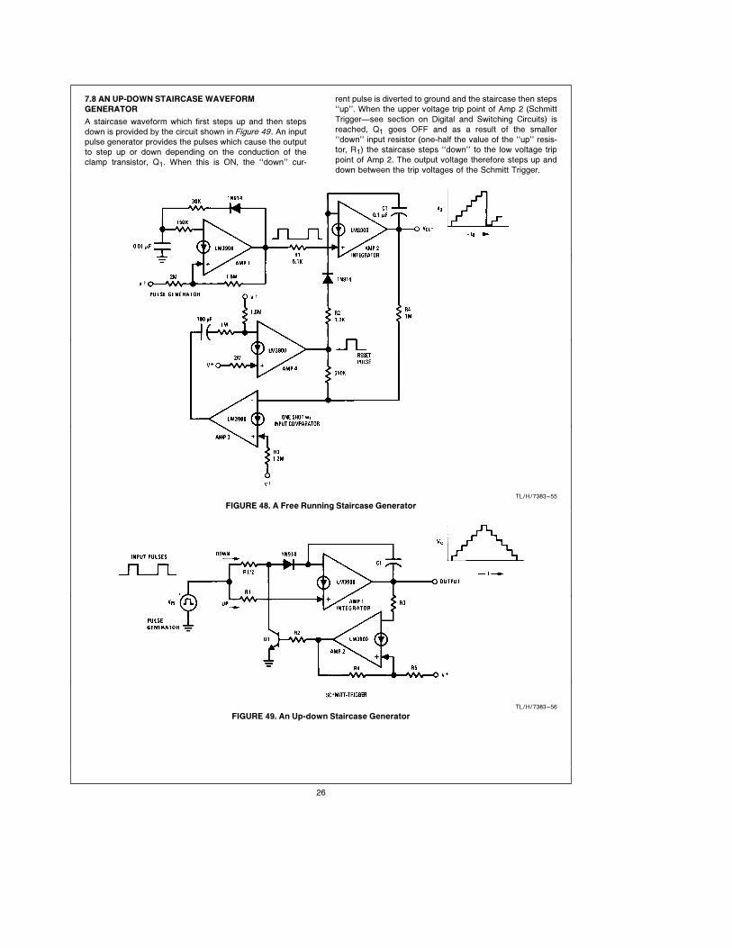
7.8 AN UP-DOWN STAIRCASE WAVEFORM
GENERATOR
A staircase waveform which first steps up and then steps
down is provided by the circuit shown in Figure 49. An input
pulse generator provides the pulses which cause the output
to step up or down depending on the conduction of the
clamp transistor, Q1. When this is ON, the ‘‘down’’ cur-
rent pulse is diverted to ground and the staircase then steps
‘‘up’’. When the upper voltage trip point of Amp 2 (Schmitt
TriggerÐsee section on Digital and Switching Circuits) is
reached, Q1 goes OFF and as a result of the smaller
‘‘down’’ input resistor (one-half the value of the ‘‘up’’ resis-
tor, R1) the staircase steps ‘‘down’’ to the low voltage trip
point of Amp 2. The output voltage therefore steps up and
down between the trip voltages of the Schmitt Trigger.
TL/H/7383–55
FIGURE 48. A Free Running Staircase Generator
TL/H/7383–56
FIGURE 49. An Up-down Staircase Generator
26
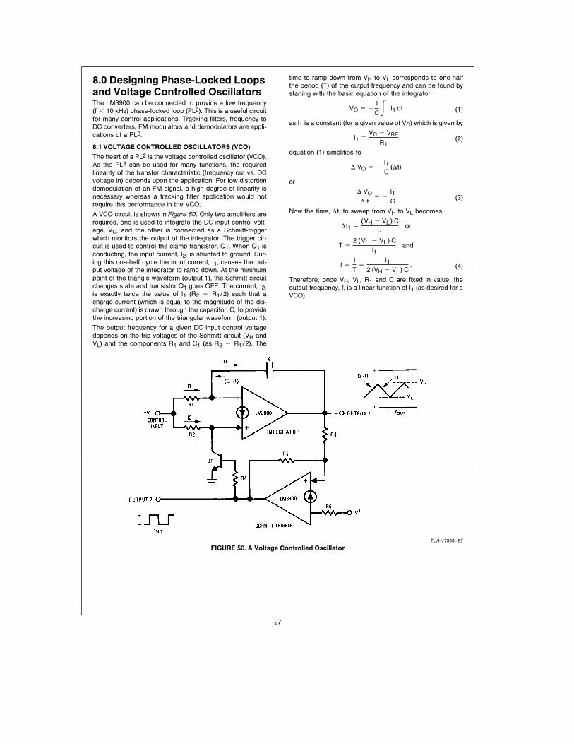
8.0 Designing Phase-Locked Loopsand Voltage Controlled OscillatorsThe LM3900 can be connected to provide a low frequency
(f k 10 kHz) phase-locked loop (PL2). This is a useful circuit
for many control applications. Tracking filters, frequency to
DC converters, FM modulators and demodulators are appli-
cations of a PL2.
8.1 VOLTAGE CONTROLLED OSCILLATORS (VCO)
The heart of a PL2 is the voltage controlled oscillator (VCO).
As the PL2 can be used for many functions, the required
linearity of the transfer characteristic (frequency out vs. DC
voltage in) depends upon the application. For low distortion
demodulation of an FM signal, a high degree of linearity is
necessary whereas a tracking filter application would not
require this performance in the VCO.
A VCO circuit is shown in Figure 50. Only two amplifiers are
required, one is used to integrate the DC input control volt-
age, VC, and the other is connected as a Schmitt-trigger
which monitors the output of the integrator. The trigger cir-
cuit is used to control the clamp transistor, Q1. When Q1 is
conducting, the input current, I2, is shunted to ground. Dur-
ing this one-half cycle the input current, I1, causes the out-
put voltage of the integrator to ramp down. At the minimum
point of the triangle waveform (output 1), the Schmitt circuit
changes state and transistor Q1 goes OFF. The current, I2,
is exactly twice the value of I1 (R2 e R1/2) such that a
charge current (which is equal to the magnitude of the dis-
charge current) is drawn through the capacitor, C, to provide
the increasing portion of the triangular waveform (output 1).
The output frequency for a given DC input control voltage
depends on the trip voltages of the Schmitt circuit (VH and
VL) and the components R1 and C1 (as R2 e R1/2). The
time to ramp down from VH to VL corresponds to one-half
the period (T) of the output frequency and can be found by
starting with the basic equation of the integrator
VO e b
1
C # I1 dt (1)
as I1 is a constant (for a given value of VC) which is given by
I1 e
VC b VBE
R1(2)
equation (1) simplifies to
D VO e b
I1
C(Dt)
or
D VO
D te b
I1
C(3)
Now the time, Dt, to sweep from VH to VL becomes
Dt1 e
(VH b VL ) C
I1or
T e
2 (VH b VL ) C
I1and
f e
1
Te
I1
2 (VH b VL ) C. (4)
Therefore, once VH, VL, R1 and C are fixed in value, the
output frequency, f, is a linear function of I1 (as desired for a
VCO).
TL/H/7383–57
FIGURE 50. A Voltage Controlled Oscillator
27
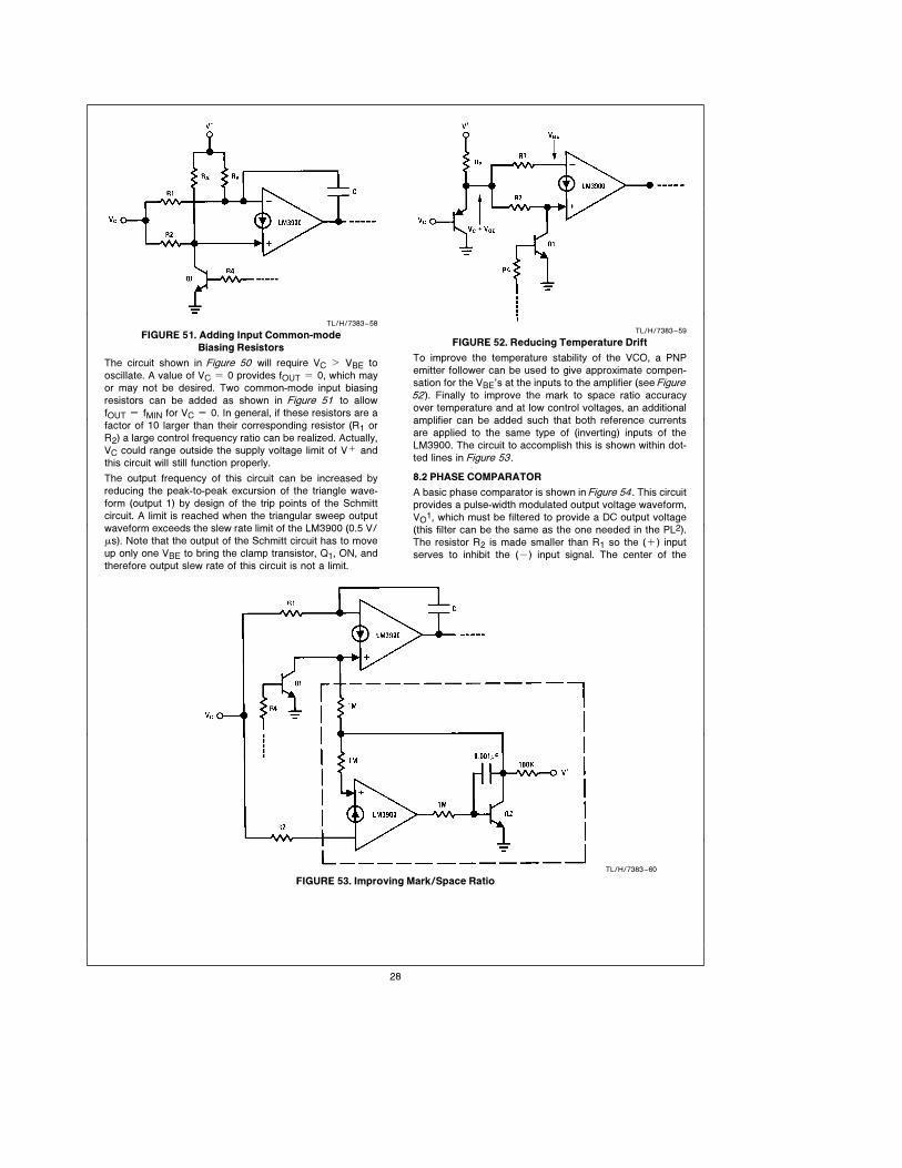
TL/H/7383–58
FIGURE 51. Adding Input Common-mode
Biasing Resistors
The circuit shown in Figure 50 will require VC l VBE to
oscillate. A value of VC e 0 provides fOUT e 0, which may
or may not be desired. Two common-mode input biasing
resistors can be added as shown in Figure 51 to allow
fOUT e fMIN for VC e 0. In general, if these resistors are a
factor of 10 larger than their corresponding resistor (R1 or
R2) a large control frequency ratio can be realized. Actually,
VC could range outside the supply voltage limit of Va and
this circuit will still function properly.
The output frequency of this circuit can be increased by
reducing the peak-to-peak excursion of the triangle wave-
form (output 1) by design of the trip points of the Schmitt
circuit. A limit is reached when the triangular sweep output
waveform exceeds the slew rate limit of the LM3900 (0.5 V/
ms). Note that the output of the Schmitt circuit has to move
up only one VBE to bring the clamp transistor, Q1, ON, and
therefore output slew rate of this circuit is not a limit.
TL/H/7383–59
FIGURE 52. Reducing Temperature Drift
To improve the temperature stability of the VCO, a PNP
emitter follower can be used to give approximate compen-
sation for the VBE’s at the inputs to the amplifier (seeFigure52). Finally to improve the mark to space ratio accuracy
over temperature and at low control voltages, an additional
amplifier can be added such that both reference currents
are applied to the same type of (inverting) inputs of the
LM3900. The circuit to accomplish this is shown within dot-
ted lines in Figure 53.
8.2 PHASE COMPARATOR
A basic phase comparator is shown inFigure 54. This circuit
provides a pulse-width modulated output voltage waveform,
VO1, which must be filtered to provide a DC output voltage
(this filter can be the same as the one needed in the PL2).
The resistor R2 is made smaller than R1 so the (a) input
serves to inhibit the (b) input signal. The center of the
TL/H/7383–60
FIGURE 53. Improving Mark/Space Ratio
28
dynamic range is indicated by the waveforms shown on the
figure (90§ phase difference between fIN and fVCO).
RANGE OF VODC
Va
2s VODC s Va
TL/H/7383–61
FIGURE 54. Phase Comparator
The filtered DC output voltage will center at 3Va/4 and can
range from Va/2 to Va as the phase error ranges from 0
degrees to 180 degrees.
8.3 A COMPLETE PHASE-LOCKED LOOP
A phase-locked loop can be realized with three of the ampli-
fiers as shown in Figure 55. This has a center frequency of
approximately 3 kHz. To increase the lock range, DC gain
can be added at the input to the VCO by using the fourth
amplifier of the LM3900. If the gain is inverting, the limited
DC dynamic range out of the phase detector can be in-
creased to improve the frequency lock range. With inverting
gain, the input to the VCO could go to zero volts. This will
cause the output of the VCO to go high (Va) and will latch if
applied to the (a) input of the phase comparator. Therefore
apply the VCO signal to the (b) input of the phase compar-
ator or add the common-mode biasing resistors of Figure51.
8.4 CONCLUSIONS
One LM3900 package (4 amplifiers) can provide all of the
operations necessary to make a phase-locked loop. In addi-
tion, a VCO is a generally useful component for other sys-
tem applications.
9.0 Designing Digital and SwitchingCircuitsThe amplifiers of the LM3900 can be over-driven and used
to provide a large number of low speed digital and switching
circuit applications for control systems which operate off of
single power supply voltages larger than the standarda5 VDC digital limit. The large voltage swing and slower
speed are both advantages for most industrial control sys-
tems. Each amplifier of the LM3900 can be thought of as ‘‘a
super transistor’’ with a b of 1,000,000 (25 nA input current
and 25 mA output current) and with a non-inverting input
feature. In addition, the active pull-up and pull-down which
exists at the output will supply larger currents than the sim-
ple resistor pull-ups which are used in digital logic gates.
Finally, the low input currents allow timing circuits which
minimize the capacitor values as large impedance levels
can be used with the LM3900.
TL/H/7383–62
FIGURE 55. A Phase-locked Loop
29
9.1 AN ‘‘OR’’ GATE
An OR gate can be realized by the circuit shown in Figure56. A resistor (150 kX) from Va to the (b) input keeps the
output of the amplifier in a low voltage saturated state for all
inputs A, B, and C at 0V. If any one of the input signals were
to go high (j Va) the current flow through the 75 kX input
resistor will cause the amplifier to switch to the positive out-
put saturation state (VO j Va). The current loss through
the other input resistors (which have an input in the low
voltage state) represents an insignificant amount of the total
input current which is provided by the, at least one, high
voltage input. More than three inputs can be OR’ed if de-
sired.
f e AaBaC
TL/H/7383–63
FIGURE 56. An ‘‘OR’’ Gate
The ‘‘fan-out’’ or logical drive capability is large (50 gates if
each gate input has a 75 kX resistor) due to the 10 mA
output current capability of the LM3900. A NOR gate can be
obtained by interchanging the inputs to the LM3900.
9.2 AN ‘‘AND’’ GATE
A three input AND gate is shown in Figure 57. This gate
requires all three inputs to be high in order to have sufficient
current entering the (a) input to cause the output of the
amplifier to switch high. The addition of R2 causes a smaller
current to enter the (a) input when only two of the inputs
are high. (A two input AND gate would not require a resistor
f e A#B#CTL/H/7383–64
FIGURE 57. An ‘‘AND’’ Gate
as R2). More than three inputs becomes difficult with this
resistor summing approach as the (a) input is too close to
having the necessary current to switch just prior to the last
input going high. For a larger fan-in an input diode network
(similar to DTL) is recommended as shown in Figure 58.
Interchange the inputs for a NAND gate.
f e A#B#C#D#E#F
All Diodes 1N914 or Equiv. TL/H/7383–65
FIGURE 58. A Large Fan-in ‘‘AND’’ Gate
9.3 A BI-STABLE MULTIVIBRATOR
A bi-stable multivibrator (as asynchronous RS flip-flop) can
be realized as shown in Figure 59. Positive feedback is pro-
vided by resistor R4 which causes the latching. A positive
pulse at the ‘‘set’’ input causes the output to go high and a
‘‘reset’’ positive pulse will return the output to essentially
0VDC.
TL/H/7383–66
FIGURE 59. A Bi-stable Multivibrator
30
9.4 TRIGGER FLIP FLOPS
Trigger flip flops are useful to divide an input frequency as
each input pulse will cause the output of a trigger flip flop to
change state. Again, due to the absence of a clocking signal
input, this is for an asynchronous logic application. A circuit
which uses only one amplifier is shown in Figure 60. Steer-
ing of the differentiated positive input trigger is provided by
the diode CR2. For a low output voltage state, CR2 shunts
the trigger away from the (b) input and resistor R3 couples
this positive input trigger to the (a) input terminal. This
causes the output to switch high. The high voltage output
state now keeps CR2 OFF and the smaller value of (R5 a
R6) compared with R3 causes a larger positive input trigger
to be coupled to the (b) input which causes the output to
switch to the low voltage state.
A second trigger flip flop can be made which consists of two
amplifiers and also provides a complementary output. This
connection is shown in Figure 61.
9.5 MONOSTABLE MULTIVIBRATORS (ONE-SHOTS)
Monostable multivibrators can be made using one or two of
the amplifiers of the LM3900. In addition, the output can be
designed to be either high or low in the quiescent state.
Further, to increase the usefulness, a one-shot can be de-
signed which triggers at a particular DC input voltage level
to serve the dual role of providing first a comparator and
then a pulse generator.
TL/H/7383–67
FIGURE 60. A Trigger Flip Flop
TL/H/7383–68
FIGURE 61. A Two-amplifier Trigger Flip Flop
31

# Speeds Recovery
PW t 2 c 10C
TL/H/7383–69
FIGURE 62. A One-shot Multivibrator
9.5.1 A TWO-AMPLIFIER ONE-SHOT
A circuit for a two-amplifier one-shot is shown in Figure 62.
As the resistor, R2, from Va to the (b) input is smaller than
R5 (from Va to the (a) input), amplifier 2 will be biased to a
low-voltage output in the quiescent state. As a result, no
current is supplied to the (b) input of amplifier 1 (via R3)
which causes the output of this amplifier to be in the high
voltage state. Capacitor C1 therefore has essentially the full
Va supply voltage across it (Vab2 VBE). Now when a dif-
ferentiated trigger (due to C2) causes amplifier 1 to be driv-
en ON (output voltage drops to essentially zero volts) this
negative transient is coupled (via C1) to the (b) input of
amplifier 2 which causes the output of this amplifier to be
driven high (to positive saturation). This condition remains
while C1 discharges via (R1) from approximately Va to ap-
proximately Va/2. This time interval is the pulse width
(PW). After C1 no longer diverts sufficient current of R2away from the (b) input of amplifier 2 (i.e., C1 is discharged
to approximately Va/2 V) the stable DC state is restoredÐ
amplifier 2 output low and amplifier 1 output high.
This circuit can be rapidly re-triggered due to the action of
the diode, CR1. This re-charges C1 as amplifier 1 drives full
output current capability (approximately 10 mA) through C1,
CR1 and into the saturated (b) input of amplifier 2 to
ground. The only time limit is the 10 mA available from am-
plifier 1 and the value of C1. If a rapid reset is not required,
CR1 can be omitted.
Trips At VIN j 0.8 Va
VIN must fall k 0.8 Va prior to t2
TL/H/7383–70
FIGURE 63. A One-shot Multivibrator
with an Input Comparator
9.5.2 A COMBINATION ONE-SHOT/COMPARATOR
CIRCUIT
In many applications a pulse is required if a DC input signal
exceeds a predetermined value. This exists in free-running
oscillators where after a particular output level has been
reached a reset pulse must be generated to recycle the
oscillator. This double function is provided with the circuit of
Figure 63. The resistors R5 and R6 of amplifier 1 provide the
inputs to a comparator and, as shown, an input signal, VIN,
is compared with the supply voltage, Va. The output volt-
age of amplifier 1 is normally in a high voltage state and will
fall and initiate the generation of the output pulse when VINis R6/R5 Va or approximately 80% of Va. To keep VINfrom disturbing the pulse generation it is required that VINfall to less than the trip voltage prior to the termination of
the output pulse. This is the case when this circuit is used to
generate a reset pulse and therefore this causes no prob-
lems.
9.5.3 A ONE-AMPLIFIER ONE-SHOT (POSITIVE PULSE)
A one-shot circuit can be realized using only one amplifier
as shown in Figure 64.
The resistor R2 keeps the output in the low voltage state. A
differentiated positive trigger causes the output to switch to
the high voltage state and resistor R5 latches this state. The
capacitor, C1, charges from essentially ground to approxi-
mately Va/4 where the circuit latches back to the quiescent
state. The diode, CR1, is used to allow a rapid re-triggering.
TL/H/7383–71
FIGURE 64. A One-amplifier One-shot (Positive Output)
32
9.5.4 A ONE-AMPLIFIER ONE-SHOT (NEGATIVE PULSE)
A one-amplifier one-shot multivibrator which has a quies-
cent state with the output high and which falls to zero volts
for the pulse duration is shown in Figure 65.
TL/H/7383–72
FIGURE 65. A One-Amplifier One-Shot
(Negative Output)
The sum of the currents through R2 and R3 keeps the (b)
input at essentially ground. This causes VO to be in the high
voltage state. A differentiated negative trigger waveform
causes the output to switch to the low voltage state. The
large voltage across C1 now provides input current via R1 to
keep the output low until C1 is discharged to approximately
Va/10. At this time the output switches to the stable high
voltage state.
If the R4C2 network is moved to the (b) input terminal, the
circuit will trigger on a differentiated positive trigger wave-
form.
9.6 COMPARATORS
The voltage comparator is a function required for most sys-
tem operations and can easily be performed by the LM3900.
Both an inverting and a non-inverting comparator can be
obtained.
9.6.1 A COMPARATOR FOR POSITIVE
INPUT VOLTAGES
The circuit inFigure 66 is an inverting comparator. To insure
proper operation, the reference voltage must be larger than
Voltage Limit
No Positive
TL/H/7383–73
FIGURE 66. An Inverting Voltage Comparator
VBE, but there is no upper limit as long as the input resistor
is large enough to guarantee that the input current will not
exceed 200 mA.
9.6.2 A COMPARATOR FOR NEGATIVE
INPUT VOLTAGES
Adding a common-mode biasing network to the comparator
inFigure 66 makes it possible to compare voltages between
zero and one volt as well as the comparison of rather large
negative voltages, Figure 67. When working with negative
voltages, the current supplied by the common-mode net-
work must be large enough to satisfy both the current drain
demands of the input voltages and the bias current require-
ment of the amplifier.
No Negative
Voltage Limit
If Properly
Biased
TL/H/7383–74
FIGURE 67. A Non-inverting Low-voltage Comparator
9.6.3 A POWER COMPARATOR
When used in conjunction with an external transistor, this
power comparator will drive loads which require more cur-
rent than the IC amplifier is capable of supplying. Figure 68shows a non-inverting comparator which is capable of driv-
ing a 12V, 40 mA panel lamp.
TL/H/7383–75
FIGURE 68. A Non-inverting Power Comparator
9.6.4 A MORE PRECISE COMPARATOR
A more precise comparator can be designed by using a sec-
ond amplifier such that the input voltages of the same type
of inputs are compared. The (b) input voltages of two am-
plifiers are naturally more closely matched initially and track
well with temperature changes. The comparator of Figure69 uses this concept.
33
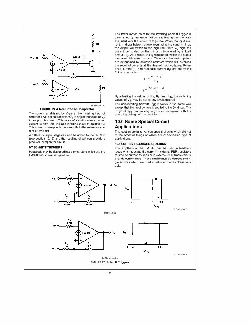
TL/H/7383–76
FIGURE 69. A More Precise Comparator
The current established by VREF at the inverting input of
amplifier 1 will cause transistor Q1 to adjust the value of VAto supply this current. This value of VA will cause an equal
current to flow into the non-inverting input of amplifier 2.
This current corresponds more exactly to the reference cur-
rent of amplifier 1.
A differential input stage can also be added to the LM3900
(see section 10.16) and the resulting circuit can provide a
precision comparator circuit.
9.7 SCHMITT TRIGGERS
Hysteresis may be designed into comparators which use the
LM3900 as shown in Figure 70.
The lower switch point for the inverting Schmitt-Trigger is
determined by the amount of current flowing into the posi-
tive input with the output voltage low. When the input cur-
rent, I3, drops below the level required by the current mirror,
the output will switch to the high limit. With VO high, the
current demanded by the mirror is increased by a fixed
amount, I2. As a result, the I3 required to switch the output
increases this same amount. Therefore, the switch points
are determined by selecting resistors which will establish
the required currents at the desired input voltages. Refer-
ence current (I1) and feedback current (I2) are set by the
following equation.
I1 e
Va b w
RB
I2 e
VO MAX b w
RF
By adjusting the values of RB, RF, and RIN, the switching
values of VIN may be set to any levels desired.
The non-inverting Schmitt Trigger works in the same way
except that the input voltage is applied to the (a) input. The
range of VIN may be very large when compared with the
operating voltage of the amplifier.
10.0 Some Special CircuitApplicationsThis section contains various special circuits which did not
fit the order of things or which are one-of-a-kind type of
applications.
10.1 CURRENT SOURCES AND SINKS
The amplifiers of the LM3900 can be used in feedback
loops which regulate the current in external PNP transistors
to provide current sources or in external NPN transistors to
provide current sinks. These can be multiple sources or sin-
gle sources which are fixed in value or made voltage vari-
able.
TL/H/7383–77
(a) Inverting
TL/H/7383–78
(b) Non-inverting
FIGURE 70. Schmitt Triggers
34
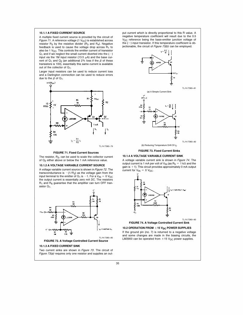
10.1.1 A FIXED CURRENT SOURCE
A multiple fixed current source is provided by the circuit of
Figure 71. A reference voltage (1 VDC) is established across
resistor R3 by the resistive divider (R3 and R4). Negative
feedback is used to cause the voltage drop across R1 to
also be 1 VDC. This controls the emitter current of transistor
Q1 and if we neglect the small current diverted into the (b)
input via the 1M input resistor (13.5 mA) and the base cur-
rent of Q1 and Q2 (an additional 2% loss if the b of these
transistors is 100), essentially this same current is available
out of the collector of Q1.
Larger input resistors can be used to reduce current loss
and a Darlington connection can be used to reduce errors
due to the b of Q1.
I2 e
R1
R2I1
TL/H/7383–79
FIGURE 71. Fixed Current Sources
The resistor, R2, can be used to scale the collector current
of Q2 either above or below the 1 mA reference value.
10.1.2 A VOLTAGE VARIABLE CURRENT SOURCE
A voltage variable current source is shown inFigure 72. The
transconductance is b(1/R2) as the voltage gain from the
input terminal to the emitter of Q1 is b1. For a VIN e 0 VDCthe output current is essentially zero mA DC. The resistors
R1 and R6 guarantee that the amplifier can turn OFF tran-
sistor Q1.
TL/H/7383–80
FIGURE 72. A Voltage Controlled Current Source
10.1.3 A FIXED CURRENT SINK
Two current sinks are shown in Figure 73. The circuit of
Figure 73(a) requires only one resistor and supplies an out-
put current which is directly proportional to this R value. A
negative temperature coefficient will result due to the 0.5
VDC reference being the base-emitter junction voltage of
the (b) input transistor. If this temperature coefficient is ob-
jectionable, the circuit of Figure 73(b) can be employed.
TL/H/7383–81
(a) A Simple Current Sink
TL/H/7383–82
(b) Reducing Temperature Drift Of IO
FIGURE 73. Fixed Current Sinks
10.1.4 A VOLTAGE VARIABLE CURRENT SINK
A voltage variable current sink is shown in Figure 74. The
output current is 1 mA per volt of VIN (as R5 e 1 kX and the
gain is a1). This circuit provides approximately 0 mA output
current for VIN e 0 VDC.
TL/H/7383–83
FIGURE 74. A Voltage Controlled Current Sink
10.2 OPERATION FROM g15 VDC POWER SUPPLIES
If the ground pin (no. 7) is returned to a negative voltage
and some changes are made in the biasing circuits, the
LM3900 can be operated from g15 VDC power supplies.
35
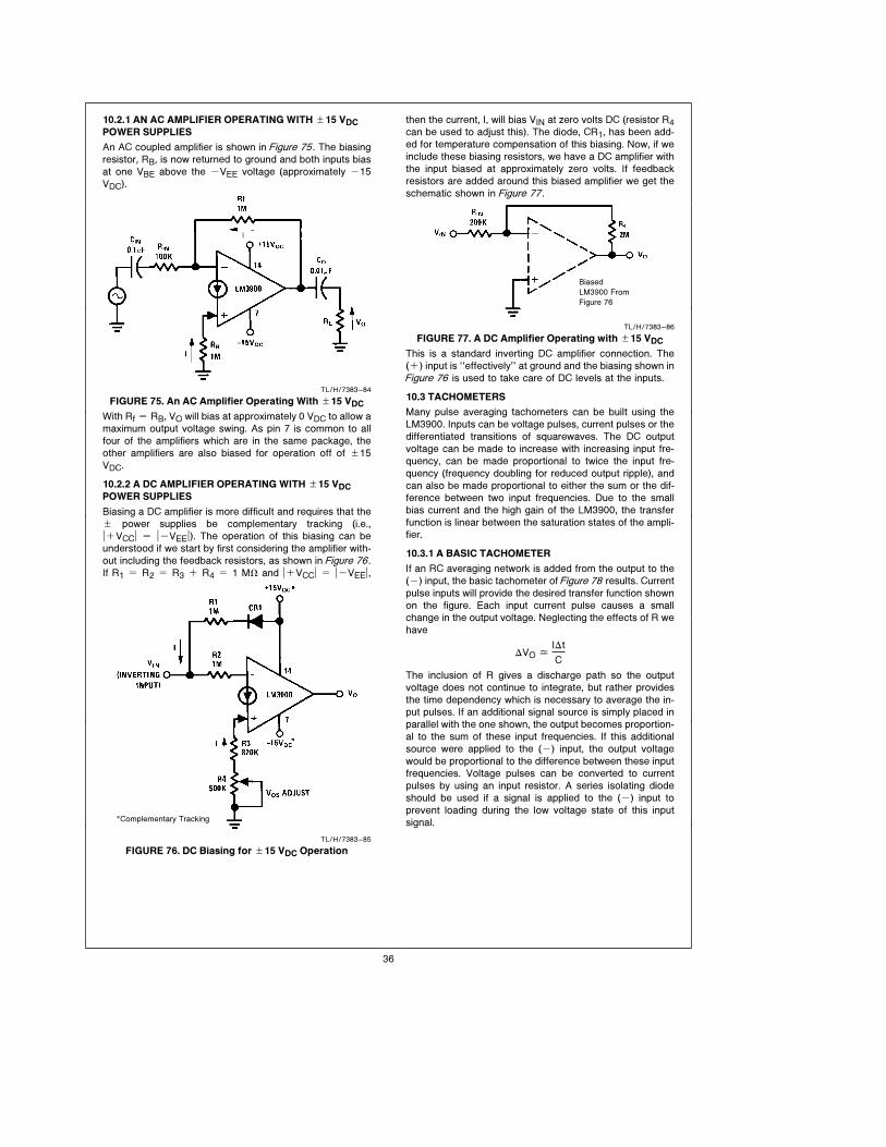
10.2.1 AN AC AMPLIFIER OPERATING WITH g15 VDCPOWER SUPPLIES
An AC coupled amplifier is shown in Figure 75. The biasing
resistor, RB, is now returned to ground and both inputs bias
at one VBE above the bVEE voltage (approximately b15
VDC).
TL/H/7383–84
FIGURE 75. An AC Amplifier Operating With g15 VDC
With Rf e RB, VO will bias at approximately 0 VDC to allow a
maximum output voltage swing. As pin 7 is common to all
four of the amplifiers which are in the same package, the
other amplifiers are also biased for operation off of g15
VDC.
10.2.2 A DC AMPLIFIER OPERATING WITH g15 VDCPOWER SUPPLIES
Biasing a DC amplifier is more difficult and requires that theg power supplies be complementary tracking (i.e.,
laVCCl e lbVEEl). The operation of this biasing can be
understood if we start by first considering the amplifier with-
out including the feedback resistors, as shown in Figure 76.
If R1 e R2 e R3 a R4 e 1 MX and laVCCl e lbVEEl,
*Complementary Tracking
TL/H/7383–85
FIGURE 76. DC Biasing for g15 VDC Operation
then the current, I, will bias VIN at zero volts DC (resistor R4can be used to adjust this). The diode, CR1, has been add-
ed for temperature compensation of this biasing. Now, if we
include these biasing resistors, we have a DC amplifier with
the input biased at approximately zero volts. If feedback
resistors are added around this biased amplifier we get the
schematic shown in Figure 77.
Biased
LM3900 From
Figure 76
TL/H/7383–86
FIGURE 77. A DC Amplifier Operating with g15 VDC
This is a standard inverting DC amplifier connection. The
(a) input is ‘‘effectively’’ at ground and the biasing shown in
Figure 76 is used to take care of DC levels at the inputs.
10.3 TACHOMETERS
Many pulse averaging tachometers can be built using the
LM3900. Inputs can be voltage pulses, current pulses or the
differentiated transitions of squarewaves. The DC output
voltage can be made to increase with increasing input fre-
quency, can be made proportional to twice the input fre-
quency (frequency doubling for reduced output ripple), and
can also be made proportional to either the sum or the dif-
ference between two input frequencies. Due to the small
bias current and the high gain of the LM3900, the transfer
function is linear between the saturation states of the ampli-
fier.
10.3.1 A BASIC TACHOMETER
If an RC averaging network is added from the output to the
(b) input, the basic tachometer ofFigure 78 results. Current
pulse inputs will provide the desired transfer function shown
on the figure. Each input current pulse causes a small
change in the output voltage. Neglecting the effects of R we
have
DVO jIDt
C
The inclusion of R gives a discharge path so the output
voltage does not continue to integrate, but rather provides
the time dependency which is necessary to average the in-
put pulses. If an additional signal source is simply placed in
parallel with the one shown, the output becomes proportion-
al to the sum of these input frequencies. If this additional
source were applied to the (b) input, the output voltage
would be proportional to the difference between these input
frequencies. Voltage pulses can be converted to current
pulses by using an input resistor. A series isolating diode
should be used if a signal is applied to the (b) input to
prevent loading during the low voltage state of this input
signal.
36
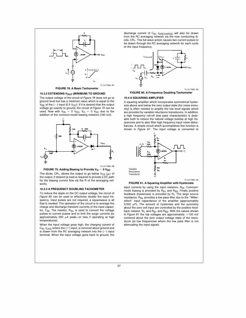
TL/H/7383–87
FIGURE 78. A Basic Tachometer
10.3.2 EXTENDING VOUT (MINIMUM) TO GROUND
The output voltage of the circuit of Figure 78 does not go to
ground level but has a minimum value which is equal to the
VBE of the (b) input (0.5 VDC). If it is desired that the output
voltage go exactly to ground, the circuit of Figure 79 can be
used. Now with VIN e 0 VDC, VO e 0 VDC due to the
addition of the common-mode biasing resistors (180 kX).
TL/H/7383–88
FIGURE 79. Adding Biasing to Provide VO e 0 VDC
The diode, CR1, allows the output to go below VCE SAT of
the output, if desired (a load is required to provide a DC path
for the biasing current flow via the R of the averaging net-
work).
10.3.3 A FREQUENCY DOUBLING TACHOMETER
To reduce the ripple on the DC output voltage, the circuit of
Figure 80 can be used to effectively double the input fre-
quency. Input pulses are not required, a squarewave is all
that is needed. The operation of the circuit is to average the
charge and discharge transient currents of the input capaci-
tor, CIN. The resistor, RIN, is used to convert the voltage
pulses to current pulses and to limit the surge currents (to
approximately 200 mA peakÐor less if operating at high
temperatures).
When the input voltage goes high, the charging current of
CIN, ICHG enters the (a) input, is mirrored about ground and
is drawn from the RC averaging network into the (b) input
terminal. When the input voltage goes back to ground, the
discharge current of CIN, IDISCHARGE will also be drawn
from the RC averaging network via the now conducting di-
ode, CR1. This full wave action causes two current pulses to
be drawn through the RC averaging network for each cycle
of the input frequency.
TL/H/7383–89
FIGURE 80. A Frequency Doubling Tachometer
10.4 A SQUARING AMPLIFIER
A squaring amplifier which incorporates symmetrical hyster-
esis above and below the zero output state (for noise immu-
nity) is often needed to amplify the low level signals which
are provided by variable reluctance transducers. In addition,
a high frequency roll-off (low pass characteristic) is desir-
able both to reduce the natural voltage buildup at high fre-
quencies and to also filter high frequency input noise distur-
bances. A simple circuit which accomplishes this function is
shown in Figure 81. The input voltage is converted to
VariableReluctanceTransducer
TL/H/7383–90
FIGURE 81. A Squaring Amplifier with Hysteresis
input currents by using the input resistors, RIN. Common-
mode biasing is provided by RB1 and RB2. Finally positive
feedback (hysteresis) is provided by Rf. The large source
resistance, RIN, provides a low pass filter due to the ‘‘Miller-
effect’’ input capacitance of the amplifier (approximately
0.002 mF). The amount of hysteresis and the symmetry
about the zero volt input are controlled by the positive feed-
back resistor, Rf, and RB1 and RB2. With the values shown
in Figure 81 the trip voltages are approximately g150 mV
centered about the zero output voltage state of the trans-
ducer (at low frequencies where the low pass filter is not
attenuating the input signal).
37
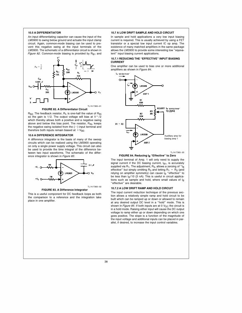
10.5 A DIFFERENTIATOR
An input differentiating capacitor can cause the input of the
LM3900 to swing below ground and actuate the input clamp
circuit. Again, common-mode biasing can be used to pre-
vent this negative swing at the input terminals of the
LM3900. The schematic of a differentiator circuit is shown in
Figure 82. Common-mode biasing is provided by RB1 and
AV e
1
2
TL/H/7383–91
FIGURE 82. A Differentiator Circuit
RB2. The feedback resistor, Rf, is one-half the value of RINso the gain is 1/2. The output voltage will bias at Va/2
which thereby allows both a positive and a negative swing
above and below this bias point. The resistor, RIN, keeps
the negative swing isolated from the (b) input terminal and
therefore both inputs remain biased at aVBE.
10.6 A DIFFERENCE INTEGRATOR
A difference integrator is the basis of many of the sweep
circuits which can be realized using the LM3900 operating
on only a single power supply voltage. This circuit can also
be used to provide the time integral of the difference be-
tween two input waveforms. The schematic of the differ-
ence integrator is shown in Figure 83.
TL/H/7383–92
FIGURE 83. A Difference Integrator
This is a useful component for DC feedback loops as both
the comparison to a reference and the integration take
place in one amplifier.
10.7 A LOW DRIFT SAMPLE AND HOLD CIRCUIT
In sample and hold applications a very low input biasing
current is required. This is usually achieved by using a FET
transistor or a special low input current IC op amp. The
existence of many matched amplifiers in the same package
allows the LM3900 to provide some interesting low ‘‘equiva-
lent’’ input biasing current applications.
10.7.1 REDUCING THE ‘‘EFFECTIVE’’ INPUT BIASING
CURRENT
One amplifier can be used to bias one or more additional
amplifiers as shown in Figure 84.
biasing amp 1
Auxilliary amp for
TL/H/7383–93
FIGURE 84. Reducing IB ‘‘Effective’’ to Zero
The input terminal of Amp. 1 will only need to supply the
signal current if the DC biasing current, IB1, is accurately
supplied via R1. The adjustment, R3, allows a zeroing of ‘‘IBeffective’’ but simply omitting R3 and letting R1 e R2 (and
relying on amplifier symmetry) can cause IB ‘‘effective’’ to
be less than IB/10 (3 nA). This is useful in circuit applica-
tions such as sample and hold, where small values of IB‘‘effective’’ are desirable.
10.7.2 A LOW DRIFT RAMP AND HOLD CIRCUIT
The input current reduction technique of the previous sec-
tion allows a relatively simple ramp and hold circuit to be
built which can be ramped up or down or allowed to remain
at any desired output DC level in a ‘‘hold’’ mode. This is
shown in Figure 85. If both inputs are at 0 VDC the circuit is
in a hold mode. Raising either input will cause the DC output
voltage to ramp either up or down depending on which one
goes positive. The slope is a function of the magnitude of
the input voltage and additional inputs can be placed in par-
allel, if desired, to increase the input control variables.
38
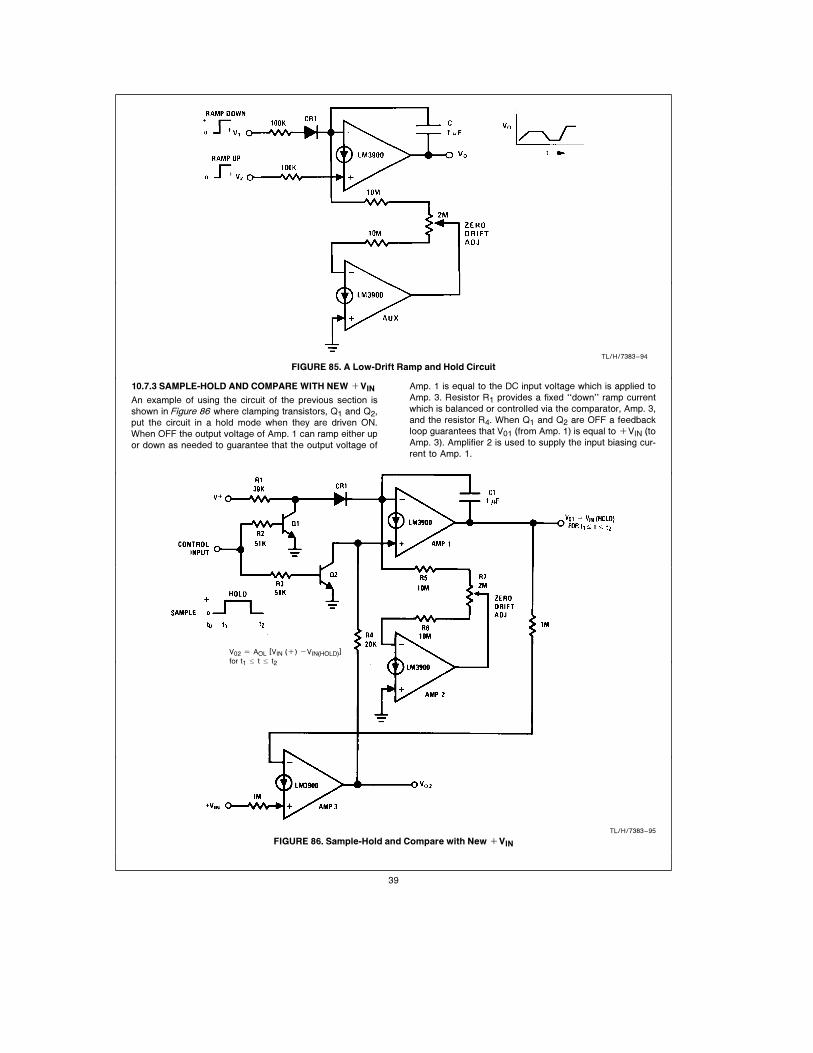
TL/H/7383–94
FIGURE 85. A Low-Drift Ramp and Hold Circuit
10.7.3 SAMPLE-HOLD AND COMPARE WITH NEW aVIN
An example of using the circuit of the previous section is
shown in Figure 86 where clamping transistors, Q1 and Q2,
put the circuit in a hold mode when they are driven ON.
When OFF the output voltage of Amp. 1 can ramp either up
or down as needed to guarantee that the output voltage of
Amp. 1 is equal to the DC input voltage which is applied to
Amp. 3. Resistor R1 provides a fixed ‘‘down’’ ramp current
which is balanced or controlled via the comparator, Amp. 3,
and the resistor R4. When Q1 and Q2 are OFF a feedback
loop guarantees that V01 (from Amp. 1) is equal to aVIN (to
Amp. 3). Amplifier 2 is used to supply the input biasing cur-
rent to Amp. 1.
V02 e AOL [VIN (a) bVIN(HOLD)]for t1 s t s t2
TL/H/7383–95
FIGURE 86. Sample-Hold and Compare with New aVIN
39

The stored voltage appears at the output, V01 of Amp. 1,
and as Amp. 3 is active, a continued comparison is made
between V01 and VIN and the output of Amp. 3 fully
switches based on this comparison. A second loop could
force VIN to be maintained at the stored value (V01) by mak-
ing use of V02 as an error signal for this second loop. There-
fore, a control system could be manually controlled to bring
it to a particular operating condition; then, by exercising the
hold control, the system would maintain this operating con-
dition due to the analog memory provided by V01.
10.8 AUDIO MIXER OR CHANNEL SELECTOR
The multiple amplifiers of the LM3900 can be used for audio
mixing (many amplifiers simultaneously providing signals
which are added to generate a composite output signal) or
for channel selection (only one channel enabled at a time).
Three amplifiers are shown being summed into a fourth am-
plifier in Figure 87.
If a power amplifier were available, all four amplifiers could
feed the single input of the power amplifier. For audio mixing
all amplifiers are simultaneously active. Particular amplifiers
can be gated OFF by making use of DC control signals
which are applied to the (a) inputs to provide a channel
select feature. As shown on Figure 87, Amp. 3 is active (as
sw 3 is closed) and Amps. 1 and 2 are driven to positive
output voltage saturation by the 5.1M which is applied to the
(a) inputs. The DC output voltage bias level of the active
amplifier is approximately 0.8 VDC and could be raised if
larger signal levels were to be accommodated. Frequency
shaping networks can be added either to the individual am-
plifiers or to the common amplifier, as desired. Switching
transients may need to be filtered at the DC control points if
the output amplifier is active during the switching intervals.
TL/H/7383–96
FIGURE 87. Audio Mixing or Selection
40
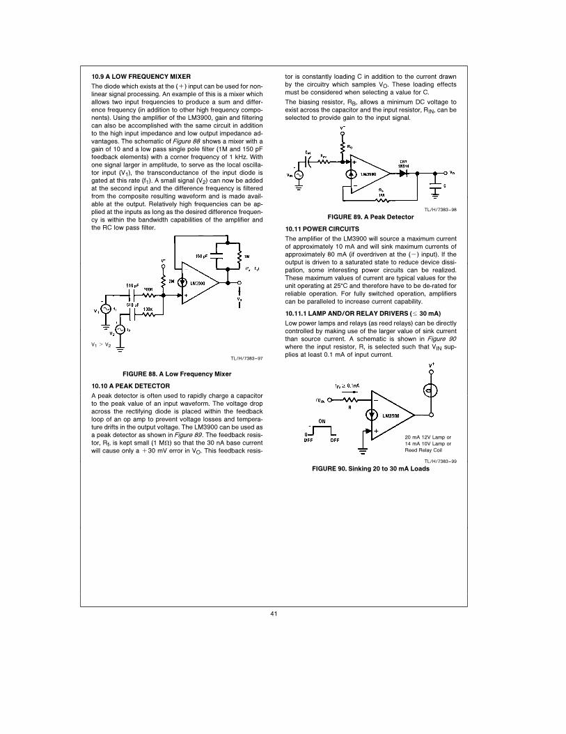
10.9 A LOW FREQUENCY MIXER
The diode which exists at the (a) input can be used for non-
linear signal processing. An example of this is a mixer which
allows two input frequencies to produce a sum and differ-
ence frequency (in addition to other high frequency compo-
nents). Using the amplifier of the LM3900, gain and filtering
can also be accomplished with the same circuit in addition
to the high input impedance and low output impedance ad-
vantages. The schematic of Figure 88 shows a mixer with a
gain of 10 and a low pass single pole filter (1M and 150 pF
feedback elements) with a corner frequency of 1 kHz. With
one signal larger in amplitude, to serve as the local oscilla-
tor input (V1), the transconductance of the input diode is
gated at this rate (f1). A small signal (V2) can now be added
at the second input and the difference frequency is filtered
from the composite resulting waveform and is made avail-
able at the output. Relatively high frequencies can be ap-
plied at the inputs as long as the desired difference frequen-
cy is within the bandwidth capabilities of the amplifier and
the RC low pass filter.
TL/H/7383–97
V1 l V2
FIGURE 88. A Low Frequency Mixer
10.10 A PEAK DETECTOR
A peak detector is often used to rapidly charge a capacitor
to the peak value of an input waveform. The voltage drop
across the rectifying diode is placed within the feedback
loop of an op amp to prevent voltage losses and tempera-
ture drifts in the output voltage. The LM3900 can be used as
a peak detector as shown in Figure 89. The feedback resis-
tor, Rf, is kept small (1 MX) so that the 30 nA base current
will cause only a a30 mV error in VO. This feedback resis-
tor is constantly loading C in addition to the current drawn
by the circuitry which samples VO. These loading effects
must be considered when selecting a value for C.
The biasing resistor, RB, allows a minimum DC voltage to
exist across the capacitor and the input resistor, RIN, can be
selected to provide gain to the input signal.
TL/H/7383–98
FIGURE 89. A Peak Detector
10.11 POWER CIRCUITS
The amplifier of the LM3900 will source a maximum current
of approximately 10 mA and will sink maximum currents of
approximately 80 mA (if overdriven at the (b) input). If the
output is driven to a saturated state to reduce device dissi-
pation, some interesting power circuits can be realized.
These maximum values of current are typical values for the
unit operating at 25§C and therefore have to be de-rated for
reliable operation. For fully switched operation, amplifiers
can be paralleled to increase current capability.
10.11.1 LAMP AND/OR RELAY DRIVERS (s 30 mA)
Low power lamps and relays (as reed relays) can be directly
controlled by making use of the larger value of sink current
than source current. A schematic is shown in Figure 90where the input resistor, R, is selected such that VIN sup-
plies at least 0.1 mA of input current.
20 mA 12V Lamp or
14 mA 10V Lamp or
Reed Relay Coil
TL/H/7383–99
FIGURE 90. Sinking 20 to 30 mA Loads
41
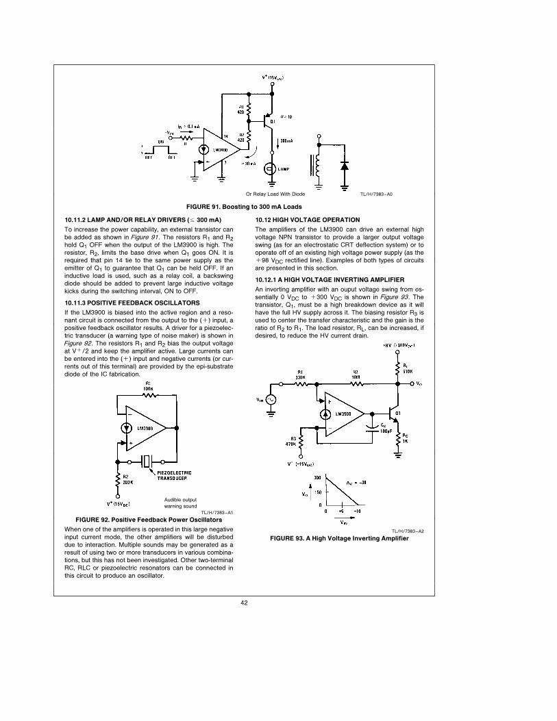
Or Relay Load With Diode TL/H/7383–A0
FIGURE 91. Boosting to 300 mA Loads
10.11.2 LAMP AND/OR RELAY DRIVERS (s 300 mA)
To increase the power capability, an external transistor can
be added as shown in Figure 91. The resistors R1 and R2hold Q1 OFF when the output of the LM3900 is high. The
resistor, R2, limits the base drive when Q1 goes ON. It is
required that pin 14 tie to the same power supply as the
emitter of Q1 to guarantee that Q1 can be held OFF. If an
inductive load is used, such as a relay coil, a backswing
diode should be added to prevent large inductive voltage
kicks during the switching interval, ON to OFF.
10.11.3 POSITIVE FEEDBACK OSCILLATORS
If the LM3900 is biased into the active region and a reso-
nant circuit is connected from the output to the (a) input, a
positive feedback oscillator results. A driver for a piezoelec-
tric transducer (a warning type of noise maker) is shown in
Figure 92. The resistors R1 and R2 bias the output voltage
at Va/2 and keep the amplifier active. Large currents can
be entered into the (a) input and negative currents (or cur-
rents out of this terminal) are provided by the epi-substrate
diode of the IC fabrication.
warning sound
Audible output
TL/H/7383–A1
FIGURE 92. Positive Feedback Power Oscillators
When one of the amplifiers is operated in this large negative
input current mode, the other amplifiers will be disturbed
due to interaction. Multiple sounds may be generated as a
result of using two or more transducers in various combina-
tions, but this has not been investigated. Other two-terminal
RC, RLC or piezoelectric resonators can be connected in
this circuit to produce an oscillator.
10.12 HIGH VOLTAGE OPERATION
The amplifiers of the LM3900 can drive an external high
voltage NPN transistor to provide a larger output voltage
swing (as for an electrostatic CRT deflection system) or to
operate off of an existing high voltage power supply (as thea98 VDC rectified line). Examples of both types of circuits
are presented in this section.
10.12.1 A HIGH VOLTAGE INVERTING AMPLIFIER
An inverting amplifier with an ouput voltage swing from es-
sentially 0 VDC to a300 VDC is shown in Figure 93. The
transistor, Q1, must be a high breakdown device as it will
have the full HV supply across it. The biasing resistor R3 is
used to center the transfer characteristic and the gain is the
ratio of R2 to R1. The load resistor, RL, can be increased, if
desired, to reduce the HV current drain.
TL/H/7383–A2
FIGURE 93. A High Voltage Inverting Amplifier
42
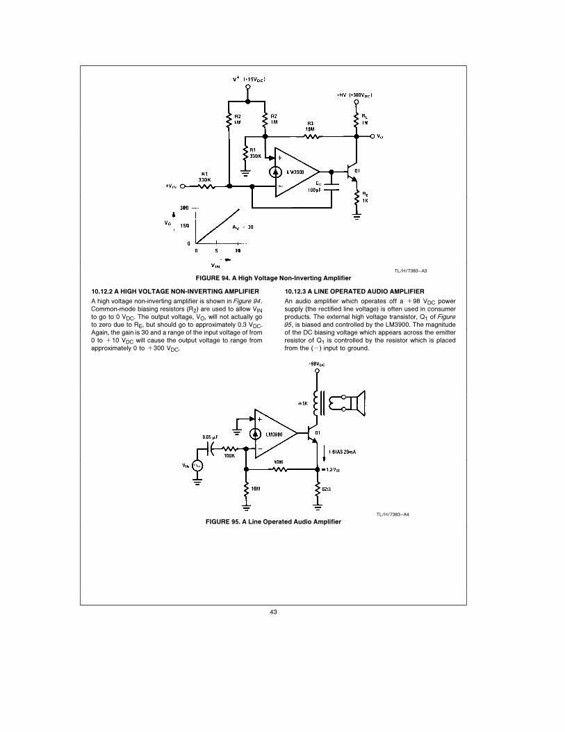
TL/H/7383–A3
FIGURE 94. A High Voltage Non-Inverting Amplifier
10.12.2 A HIGH VOLTAGE NON-INVERTING AMPLIFIER
A high voltage non-inverting amplifier is shown in Figure 94.
Common-mode biasing resistors (R2) are used to allow VINto go to 0 VDC. The output voltage, VO, will not actually go
to zero due to RE, but should go to approximately 0.3 VDC.
Again, the gain is 30 and a range of the input voltage of from
0 to a10 VDC will cause the output voltage to range from
approximately 0 to a300 VDC.
10.12.3 A LINE OPERATED AUDIO AMPLIFIER
An audio amplifier which operates off a a98 VDC power
supply (the rectified line voltage) is often used in consumer
products. The external high voltage transistor, Q1 of Figure95, is biased and controlled by the LM3900. The magnitude
of the DC biasing voltage which appears across the emitter
resistor of Q1 is controlled by the resistor which is placed
from the (b) input to ground.
TL/H/7383–A4
FIGURE 95. A Line Operated Audio Amplifier
43
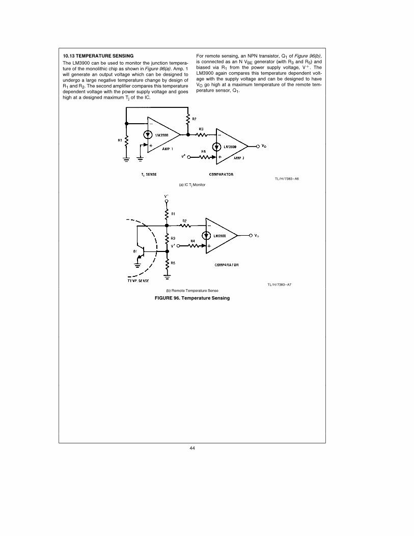
10.13 TEMPERATURE SENSING
The LM3900 can be used to monitor the junction tempera-
ture of the monolithic chip as shown in Figure 96(a) . Amp. 1
will generate an output voltage which can be designed to
undergo a large negative temperature change by design of
R1 and R2. The second amplifier compares this temperature
dependent voltage with the power supply voltage and goes
high at a designed maximum Tj of the IC.
For remote sensing, an NPN transistor, Q1 of Figure 96(b) ,is connected as an N VBE generator (with R3 and R5) and
biased via R1 from the power supply voltage, Va. The
LM3900 again compares this temperature dependent volt-
age with the supply voltage and can be designed to have
VO go high at a maximum temperature of the remote tem-
perature sensor, Q1.
TL/H/7383–A6
(a) IC Tj Monitor
TL/H/7383–A7
(b) Remote Temperature Sense
FIGURE 96. Temperature Sensing
44
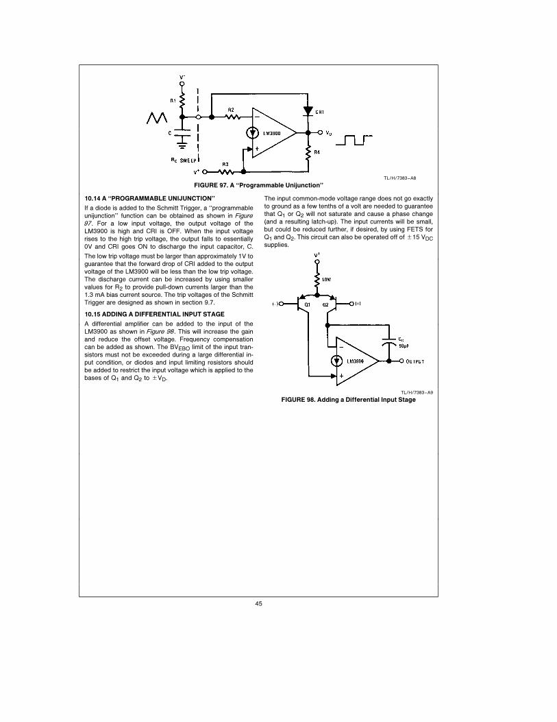
TL/H/7383–A8
FIGURE 97. A ‘‘Programmable Unijunction’’
10.14 A ‘‘PROGRAMMABLE UNIJUNCTION’’
If a diode is added to the Schmitt Trigger, a ‘‘programmable
unijunction’’ function can be obtained as shown in Figure97. For a low input voltage, the output voltage of the
LM3900 is high and CRI is OFF. When the input voltage
rises to the high trip voltage, the output falls to essentially
0V and CRI goes ON to discharge the input capacitor, C.
The low trip voltage must be larger than approximately 1V to
guarantee that the forward drop of CRI added to the output
voltage of the LM3900 will be less than the low trip voltage.
The discharge current can be increased by using smaller
values for R2 to provide pull-down currents larger than the
1.3 mA bias current source. The trip voltages of the Schmitt
Trigger are designed as shown in section 9.7.
10.15 ADDING A DIFFERENTIAL INPUT STAGE
A differential amplifier can be added to the input of the
LM3900 as shown in Figure 98. This will increase the gain
and reduce the offset voltage. Frequency compensation
can be added as shown. The BVEBO limit of the input tran-
sistors must not be exceeded during a large differential in-
put condition, or diodes and input limiting resistors should
be added to restrict the input voltage which is applied to the
bases of Q1 and Q2 to gVD.
The input common-mode voltage range does not go exactly
to ground as a few tenths of a volt are needed to guarantee
that Q1 or Q2 will not saturate and cause a phase change
(and a resulting latch-up). The input currents will be small,
but could be reduced further, if desired, by using FETS for
Q1 and Q2. This circuit can also be operated off of g15 VDCsupplies.
TL/H/7383–A9
FIGURE 98. Adding a Differential Input Stage
45
AN
-72
The
LM
3900:A
New
Curr
ent-
Diffe
rencin
gQ
uad
of
gIn
putA
mplifiers
LIFE SUPPORT POLICY
NATIONAL’S PRODUCTS ARE NOT AUTHORIZED FOR USE AS CRITICAL COMPONENTS IN LIFE SUPPORT
DEVICES OR SYSTEMS WITHOUT THE EXPRESS WRITTEN APPROVAL OF THE PRESIDENT OF NATIONAL
SEMICONDUCTOR CORPORATION. As used herein:
1. Life support devices or systems are devices or 2. A critical component is any component of a life
systems which, (a) are intended for surgical implant support device or system whose failure to perform can
into the body, or (b) support or sustain life, and whose be reasonably expected to cause the failure of the life
failure to perform, when properly used in accordance support device or system, or to affect its safety or
with instructions for use provided in the labeling, can effectiveness.
be reasonably expected to result in a significant injury
to the user.
National Semiconductor National Semiconductor National Semiconductor National SemiconductorCorporation Europe Hong Kong Ltd. Japan Ltd.1111 West Bardin Road Fax: (a49) 0-180-530 85 86 13th Floor, Straight Block, Tel: 81-043-299-2309Arlington, TX 76017 Email: cnjwge@ tevm2.nsc.com Ocean Centre, 5 Canton Rd. Fax: 81-043-299-2408Tel: 1(800) 272-9959 Deutsch Tel: (a49) 0-180-530 85 85 Tsimshatsui, KowloonFax: 1(800) 737-7018 English Tel: (a49) 0-180-532 78 32 Hong Kong
Fran3ais Tel: (a49) 0-180-532 93 58 Tel: (852) 2737-1600Italiano Tel: (a49) 0-180-534 16 80 Fax: (852) 2736-9960
National does not assume any responsibility for use of any circuitry described, no circuit patent licenses are implied and National reserves the right at any time without notice to change said circuitry and specifications.

IMPORTANT NOTICE
Texas Instruments Incorporated and its subsidiaries (TI) reserve the right to make corrections, modifications, enhancements, improvements,and other changes to its products and services at any time and to discontinue any product or service without notice. Customers shouldobtain the latest relevant information before placing orders and should verify that such information is current and complete. All products aresold subject to TI’s terms and conditions of sale supplied at the time of order acknowledgment.
TI warrants performance of its hardware products to the specifications applicable at the time of sale in accordance with TI’s standardwarranty. Testing and other quality control techniques are used to the extent TI deems necessary to support this warranty. Except wheremandated by government requirements, testing of all parameters of each product is not necessarily performed.
TI assumes no liability for applications assistance or customer product design. Customers are responsible for their products andapplications using TI components. To minimize the risks associated with customer products and applications, customers should provideadequate design and operating safeguards.
TI does not warrant or represent that any license, either express or implied, is granted under any TI patent right, copyright, mask work right,or other TI intellectual property right relating to any combination, machine, or process in which TI products or services are used. Informationpublished by TI regarding third-party products or services does not constitute a license from TI to use such products or services or awarranty or endorsement thereof. Use of such information may require a license from a third party under the patents or other intellectualproperty of the third party, or a license from TI under the patents or other intellectual property of TI.
Reproduction of TI information in TI data books or data sheets is permissible only if reproduction is without alteration and is accompaniedby all associated warranties, conditions, limitations, and notices. Reproduction of this information with alteration is an unfair and deceptivebusiness practice. TI is not responsible or liable for such altered documentation. Information of third parties may be subject to additionalrestrictions.
Resale of TI products or services with statements different from or beyond the parameters stated by TI for that product or service voids allexpress and any implied warranties for the associated TI product or service and is an unfair and deceptive business practice. TI is notresponsible or liable for any such statements.
TI products are not authorized for use in safety-critical applications (such as life support) where a failure of the TI product would reasonablybe expected to cause severe personal injury or death, unless officers of the parties have executed an agreement specifically governingsuch use. Buyers represent that they have all necessary expertise in the safety and regulatory ramifications of their applications, andacknowledge and agree that they are solely responsible for all legal, regulatory and safety-related requirements concerning their productsand any use of TI products in such safety-critical applications, notwithstanding any applications-related information or support that may beprovided by TI. Further, Buyers must fully indemnify TI and its representatives against any damages arising out of the use of TI products insuch safety-critical applications.
TI products are neither designed nor intended for use in military/aerospace applications or environments unless the TI products arespecifically designated by TI as military-grade or "enhanced plastic." Only products designated by TI as military-grade meet militaryspecifications. Buyers acknowledge and agree that any such use of TI products which TI has not designated as military-grade is solely atthe Buyer's risk, and that they are solely responsible for compliance with all legal and regulatory requirements in connection with such use.
TI products are neither designed nor intended for use in automotive applications or environments unless the specific TI products aredesignated by TI as compliant with ISO/TS 16949 requirements. Buyers acknowledge and agree that, if they use any non-designatedproducts in automotive applications, TI will not be responsible for any failure to meet such requirements.
Following are URLs where you can obtain information on other Texas Instruments products and application solutions:
Products Applications
Audio www.ti.com/audio Communications and Telecom www.ti.com/communications
Amplifiers amplifier.ti.com Computers and Peripherals www.ti.com/computers
Data Converters dataconverter.ti.com Consumer Electronics www.ti.com/consumer-apps
DLP® Products www.dlp.com Energy and Lighting www.ti.com/energy
DSP dsp.ti.com Industrial www.ti.com/industrial
Clocks and Timers www.ti.com/clocks Medical www.ti.com/medical
Interface interface.ti.com Security www.ti.com/security
Logic logic.ti.com Space, Avionics and Defense www.ti.com/space-avionics-defense
Power Mgmt power.ti.com Transportation and Automotive www.ti.com/automotive
Microcontrollers microcontroller.ti.com Video and Imaging www.ti.com/video
RFID www.ti-rfid.com
OMAP Mobile Processors www.ti.com/omap
Wireless Connectivity www.ti.com/wirelessconnectivity
TI E2E Community Home Page e2e.ti.com
Mailing Address: Texas Instruments, Post Office Box 655303, Dallas, Texas 75265Copyright © 2011, Texas Instruments Incorporated