Embed Size (px)
Citation preview

Clemson UniversityTigerPrints
All Dissertations Dissertations
8-2011
THERMOELECTRIC PROPERTIES OFNICKEL AND TITANIUM CO-INTERCALATED TITANIUM DISELENIDETimothy HolgateClemson University, [email protected]
Follow this and additional works at: https://tigerprints.clemson.edu/all_dissertations
Part of the Materials Science and Engineering Commons
This Dissertation is brought to you for free and open access by the Dissertations at TigerPrints. It has been accepted for inclusion in All Dissertations byan authorized administrator of TigerPrints. For more information, please contact [email protected].
Recommended CitationHolgate, Timothy, "THERMOELECTRIC PROPERTIES OF NICKEL AND TITANIUM CO-INTERCALATED TITANIUMDISELENIDE" (2011). All Dissertations. 810.https://tigerprints.clemson.edu/all_dissertations/810

i
THERMOELECTRIC PROPERTIES OF NICKEL AND TITANIUM CO-INTERCALATED TITANIUM DISELENIDE
A Dissertation Presented to
the Graduate School of Clemson University
In Partial Fulfillment of the Requirements for the Degree
Doctor of Philosophy Materials Science and Engineering
by Timothy Charles Holgate
August 2011
Accepted by: Dr. Terry Tritt, Committee Chair
Dr. Jian He Dr. Jian Luo
Dr. Eric Skaar Dr. Stephen Foulger

ii
ABSTRACT
Thermoelectric materials are involved in the direct conversion between thermal
and electrical energy. They may be used to generate power from a thermal gradient or to
pump heat in or out of a system when driven with DC power. Much of the recent
advances in thermoelectric research have been in materials whose thermoelectric
efficiency has been optimized at temperatures above room temperature where power
generation is the main application.
The question that I seek to answer in this dissertation is to use our standard
experimental techniques in order to assess the possibility of a class of transition metal
dichalcogenides bases on TiSe2 that are suitable candidates for thermoelectric
applications. In addition, a further question is to understand the individual roles of
intercalating titanium and nickel into the van der Waal planes of these materials and to
investigate their effects on the electrical and thermal transport properties as well as the
structure (including microstructure) of these materials.
The work presented herein has focused on deriving a thermoelectric material with
a maximum ZT in the temperature range between 100 K and room temperature. Some of
the niche applications of thermoelectric cooling in this temperature range include high-
speed computing, active cooling of detectors, and most importantly, in the region of 100
to 120 K, the viability of superconducting electronic systems without the need of
liquefied gasses.
iii
Transition metal dichalcogenides are layered structures with a weakly bonded van
der Waals gap between a-b planes. This gap may be intercalated by many different
atomic and molecular species, which may significantly affect the structural and transport
properties. Intercalation therefore provides a wide-ranging tuning “knob” for optimizing
the thermal and electrical transport properties of the host material.
Several compounds chosen from this group of materials were synthesized and
intercalated with 3d and 4d transition metals. Thermal and electrical transport properties
were measured and the best candidate, TiSe2, was chosen as the host matrix for
optimization through co-intercalation with nickel and excess titanium. Additionally, the
material was further optimized by the substitution of sulfur on selenium sites. While the
maximum thermoelectric efficiency as judge by the dimensionless figure-of-merit (ZT)
was increased, the temperature of that optimization (Tmax) was also increased to
temperatures near and above room temperature where the state-of-the-art Bi2Te3’s
efficiency has been already optimized and is much higher than those of the materials in
this work.
Though the goal of developing a material whose ZT is maximized at temperatures
below room temperature was not achieved, the overall thermoelectric efficiency of TiSe2
has been increased by the co-intercalation of nickel and titanium, and then further
increased by the substitution of selenium with sulfur. The individual roles of each of the
intercalants, as well as the substitution of sulfur, in the manipulation and optimization of
the thermal and electrical transport properties have been analyzed and understood in
terms of fundamental solid-state theory and principles and are explained herein.

iv
DEDICATION
I dedicate this dissertation to the two men who most influenced and inspired me to
love science and learning, but certainly not just the learning of science. These men have
both done so much to broaden my thinking and understanding of world and the people in
it. From them I have learned of history, politics, philosophy, patience, service, charity,
and grace. I hope that I have given to them at least a fraction of what I’ve received, or
perhaps, as I know would be their wishes, that someday I may give a full measure to
those who will come into my life as I did theirs. While serving as two of the greatest
mentors I’ve ever known, they have both become dear friends I hope to keep for life:
Wynn Mott and Jian He.

v
ACKNOWLEDGMENTS
First of all, I would like to thank my advisor and friend, Dr. Terry Tritt, who
accepted me into his group without hesitation when he was not looking to add to his
numbers. Dr. Tritt has given me many wonderful opportunities, more than generous
support, and years of friendship and mentorship. Being connected to his name alone has
done me a great service. He has played the role of friend, mentor, teacher, and worthy
adversary (in pool volleyball). To ask for more in an advisor would be like getting a
Ferrari and not liking the color.
To the rest of my committee, I am very appreciative. A heart felt thanks goes out
to Dr. Jian Luo, Dr. Stephen Foulger, Dr. Eric Skaar, and Dr. Jian He for giving up their
time to serve on my committee. Furthermore, I appreciate the support, encouragement,
and many helpful suggestions that brought this work to fruition.
I would also like to thank all of my fellow group members, past and present, who
have made my time at Clemson an enjoyable one. To Dr. Jian He, from whom I have
learned a great many things; to Dr. Liebenberg, from whom I have received a great deal
of encouragement; to Dr. Xiaohua Ji, who gave me my Chinese name; to Brad and
Justine Edwards, who made my first two years a whole lot of fun; to Su Zhe, for all the
laughs (even when I was the only one laughing); to Dr. Florin Lung, who was my first
and most interesting officemate; to Dale Hitchcock, my friend, officemate, occasional
landlord, drinking buddy, and there when I needed him; to Jennifer Graff, a great friend

vi
and thermocouple maker; to Song Zhu and his wife Milan, for all the dumplings, and to
all the others of the Tritt group, I owe my deepest gratitude.
I like to thank the collaborators, researchers, and technicians outside of Clemson
University that have contributed to this work. First and foremost, I would like to thank
Dr. Holger Kleinke of the University of Waterloo, with whom I have collaborated for
most of my graduate career. Dr. Kleinke has also been a great source of encouragement,
knowledge, and friendship. Were Canada not so cold, I would have begged for a
postdoctoral position in his group. I would further like to thank Chris Fleisher at the
University of Georgia for EPMA data and the tours of the UGA campus, as well as Dr.
Ma at the University of South Carolina’s College of Engineering and Computing for the
X-ray photoelectron spectroscopy data. My gratitude also goes out to Dr. Yonggao
(Jack) Yan at the National Institute of Standards and Technology for assistance with low
temperature heat capacity measurements.
Finally, I would like to thank the fellow graduate and undergraduate students in
my group who assisted me with sample synthesis (Matthew Hendrix), literature searches
and various calculations (Menghan Zhou), low temperature thermal conductivity
measurements (Song Zhu), and VSM measurements (Dale Hitchcock and Dr. Jian He).
You assistance was invaluable and much appreciated.

vii
TABLE OF CONTENTS TITLE PAGE....................................................................................................................... i ABSTRACT........................................................................................................................ ii DEDICATION................................................................................................................... iv ACKNOWLEDGMENTS ...................................................................................................v LIST OF TABLES............................................................................................................. ix LIST OF FIGURES ............................................................................................................ x CHAPTER I. Introduction to Thermoelectrics...................................................................1 Thermoelectric Materials .................................................................1 Seebeck and Peltier Effects..............................................................7 Thermal and Electrical Transport ..................................................11 II. Material Introduction .................................................................................27 Chalcogenides and Thermoelectrics ..............................................27 Structures of Transition Metal Dichalcogenides............................28 Charge Density Waves...................................................................30 Intercalation ...................................................................................31 The Uniqueness of Titanium Diselenide........................................32 Current Thermoelectric Studies .....................................................33 III. Measurement Systems and Techniques .....................................................38 Low Temperature Transport ..........................................................38 Seebeck and Electrical Resistivity.....................................38 Thermal Conductivity ........................................................41 Hall Coefficient..................................................................45 Specific Heat Capacity.......................................................48 High Temperature Transport..........................................................50 Seebeck and Electrical Resistivity.....................................50 Thermal Conductivity and Diffusivity...............................53 Differential Scanning Calorimetry.....................................55

viii
Table of Contents (Continued) IV. Synthesis and Processing ...........................................................................60 Sample Synthesis ...........................................................................60 Processing ......................................................................................62 Compositional Analysis .................................................................73 Sample Density ..............................................................................74 V. Structural and Compositional Analysis .....................................................67 Structure Analysis Using X-ray Diffraction ..................................67 Compositional Analysis .................................................................73 Sample Density ..............................................................................74 VI. Thermal Transport Properties ....................................................................83 Low Temperature Specific Heat Capacity of NixTi1+δSe2 .............83 Low Temperature Thermal Conductivity of NixTi1+δSe2...............84 Low Temperature Thermal Conductivity of NixTi1+δSe2-ySy .........86 VII. Electronic Transport Properties .................................................................97 Electrical Resistivity and Seebeck of NixTi1+δSe2 .........................97 Low Temperature Electrical Resistivity and Seebeck
of NixTi1+δSe2-ySy ...............................................................99 VIII. Conclusion and Final Remarks ................................................................110 APPENDICES .................................................................................................................113 A: Band Structure and Density of States Calculations .................................113 B: Magnetic Susceptibility of NixTi1+δSe2....................................................116 C: Complete Sample List..............................................................................121 REFERENCES ................................................................................................................123

ix
LIST OF TABLES Table ..................................................................................................................Page 4.1 Profile of elements used for synthesis .......................................................60 4.2 Synthesis parameters..................................................................................61 4.3 Samples synthesized ..................................................................................62 4.4 Spark plasma sintering (SPS) program parameters ...................................66 5.1 X-ray diffraction (XRD) pattern overlay of before and after SPS processing...............................................................................68 5.2 Lattice parameters calculated from high resolution XRD patterns............71
5.3 Interplanar spacing of peaks ......................................................................71 5.4 Results of the deconvolution of the (0 0 1) peak in XCh115.....................72 5.5 Nickel concentrations and secondary (0 0 1) peak positions.....................72 5.6 Electron probe microanalysis (EPMA) compositions normalized to two selenium per formula ..........................................................74 5.7 Comparison of measured to theoretical densities of two normalization schemes: one titanium; two selenium.....................75 5.8 Phase fractions used in estimating theoretical density...............................78 5.9 Comparison of measured and estimated densities using two phase scenario ................................................................................79 5.10 Contributes of each phase to the total density ...........................................79 5.11 Lattice parameters and densities of NixTi1+δSe2-ySy...................................79 6.1 Low temperature heat capacity fit parameters ...........................................84 B-1 Magnetic fit parameters of the magnetic susceptibility ...........................119 C-1 Complete sample list................................................................................121 C-2 Sample list with nominal composition, room temperature transport properties, and SPS conditions .....................................122

x
LIST OF FIGURES Figure .................................................................................................................Page
1.1 Thermopower, electrical conductivity, and power factor versus carrier concentration ..........................................................24 1.2 Sample band structure plot.........................................................................24 1.3 Density of occupied states .........................................................................25 1.4 Schematic band structures of metals, semimetals, semiconductors and insulators .................................................................................25 1.5 The Seebeck effect from a density of states perspective ...........................26 1.6 Effect of thermal and electric potential gradients on the Fermi surface .................................................................................26 1.7 Two carrier conduction under thermal and electric fields .........................26 2.1 1T and 2H polytypes of MX2.....................................................................34 2.2 Fermi surface of TiSe2 ...............................................................................35 2.3 TiSe2 band structure...................................................................................36 2.4 Trigonal unit cell of TiSe2..........................................................................37 3.1 Low temperature Seebeck and resistivity mount .......................................56 3.2 Low temperature thermal conductivity mount...........................................57 3.3 Hall coefficient measurement configuration..............................................58 3.4 Thermocouple placement on ZEM-2 .........................................................59 3.5 ZEM-2 probe configuration .......................................................................59 5.1 Overlay of XRD patters taken before and after SPS processing ...............80 5.2 (0 0 1) peak of XCh115 with one and two peak fits ..................................81 5.3 Deconvolution of the (0 0 1) peaks of XCh124 and XCh119....................82 6.1 Low temperature heat capacity with Dulong-Petit limit............................88 6.2 Heat capacity below 5 K with cp/T vs. T2 inset .........................................89 6.3 Measure and estimated density versus Debye temperature .......................90 6.4 Total thermal conductivity of NixTi1+δSe2 .................................................91 6.5 Contributions to the measured thermal conductivity .................................92 6.6 Lattice thermal conductivity of NixTi1+δSe2...............................................93 6.7 Total thermal conductivity of NixTi1+δSe2-ySy ...........................................94 6.8 Radiation corrected total thermal conductivity of NixTi1+δSe2-ySy ............95 6.9 Radiation corrected lattice thermal conductivity of NixTi1+δSe2-ySy..........96 7.1 Low temperature electrical resistivity of NixTi1+δSe2 ..............................101 7.2 Low and high temperature Seebeck Coefficient of NixTi1+δSe2-ySy with reference data.......................................................................102

xi
List of Figures (Continued) Figure .............................................................................................................................Page
7.3 Low temperature Seebeck coefficient of NixTi1+δSe2-ySy with reference data.......................................................................103 7.4 Low temperature power factor of NixTi1+δSe2 .........................................104 7.5 Low and high temperature power factor of NixTi1+δSe2 ..........................105 7.6 Effective carrier concentration versus temperature of NixTi1+δSe2..........106 7.7 Low temperature electrical resistivity of NixTi1+δSe2-ySy with reference data.......................................................................107 7.8 Low temperature Seebeck coefficient of NixTi1+δSe2-ySy with reference data.......................................................................108 7.9 Low temperature power factor of NixTi1+δSe2-ySy with reference data ...............................................................................109 8.1 Low temperature ZT of NixTi1+δSe2-ySy with reference data....................112 A-1 Density of electronic state (DOS) of TiSe2 and TiSe ..............................114 A-2 DOS of Ni0.25TiSe2 and Ti1.25Se2 .............................................................115

1
CHAPTER ONE INTRODUCTION TO THERMOELECTRICS
Thermoelectric Materials
In the May 1959 issue of Physics Today, George Vineyard wrote a book review in
which he began by telling of a report from a news correspondent from Hong Kong that
said “a strange device was being exported from Red China, capable of powering a radio
by the heat from a kerosene lamp.”1 Vineyard then pointed out that the book on which he
was writing a review contained photos, diagrams, details, and some theoretical
descriptions of this device.2 This book was actually a reprinting of two books written by
Abram Ioffe et al. and was published in Russian three years earlier. At this time,
thermoelectrics research had been underway for half a century.
In 1929, Ioffe indicated that semiconductors were the best candidates for
thermoelectric power generation. This was later reiterated by H. J. Goldsmid and R. W.
Douglas in 1954.3 To understand the attractiveness of semiconductors one must
understand how the thermal and electronic transport properties are related to the
thermoelectric efficiency of a material. In 1910, Altenkirch first attempted to describe
the thermoelectric efficiency.4 Ioffe later presented the Z parameter from which we get
the modern “dimensionless figure-of-merit”, ZT:5
2 2
ZT T Tα α σρκ κ
= = (1.1)

2
The Z parameter is simply a convenient collection of the material transport
parameters (α: Seebeck coefficient, ρ: electrical resistivity, σ: electrical conductivity, κ:
thermal conductivity, and T: temperature in Kelvin) that are used in the derivation of the
overall conversion efficiency defined as the power produced by the power supplied to the
system. For thermoelectric power generation, this becomes the electrical power output
by the system ( P EJ= , where J is the current density and E is the electric field that
consist of contributions from both Ohm’s law and the Seebeck effect: E J Tρ α= − + ∇ )
divided by the heat flux (typically in Watts/cm2) into the system ( Q TJ Tα κ= + ∇ , in
which the first term is the reversible Peltier heat term and the second is the irreversible
Fourier heat flow term.6 Note that this formulation uses the electrical linear power
density and linear thermal flux. To obtain the efficiency of the entire thermoelectric
element, the P/Q ratio must be integrated over the entire length of the element through a
change of variable— /dx dT T= ∇ :
max 0
1 11 ( )[ ]1 ( )
hot
cold
L T mhot cold
x Tcoldhot
mhot
ZTT TP Pdx dT
TQ T Q T ZTT
η=
+ −−= = =∇ + +
∫ ∫ (1.2)
Here Tm is the temperature at which ZT is a maximum, and the efficiency will
therefore be maximized when Tm is the average of Thot and Tcold ( ( ) / 2m hot coldT T T= + ). In
the limit that ZT is very large the maximum efficiency reaches the Carnot efficiency,
which is the first term in parentheses in Eqn. 1.2. It can also be seen here that
maximizing the ∆T maximized both the Carnot efficiency as well as the thermoelectric
portion of Eq. 1.2 (this, of course, ignores the fact that ZT is temperature dependent is not

3
necessarily constant across a materials under a temperature gradient). In the case of
Peltier cooling, the overall conversion efficiency, φ , is maximized by minimizing the ∆T.
This is consistent with conceptual thinking as one may imagine what happens to a Peltier
cooling system just after being switched on: immediately after, as the ∆T is zero, it is
easy to begin “pumping” heat from one side to the other.
1 ( )
( )[ ]1 1
hotm
cold cold
hot cold m
TZT
T T
T T ZTφ
+ −=
− + + (1.3)
From this representation it is clear that a good thermoelectric material will possess
a high Seebeck coefficient (α), a high electrical thermal conductivity (σ), and a low total
thermal conductivity (κ). Optimizing these parameters simultaneously has long since
proven to be quite difficult as they are interdependent. For reasons explained later in this
chapter, the Seebeck coefficient is somewhat less coupled to the thermal conductivity
whereas the electrical and thermal conductivities are coupled, since the electrons can
carry energy (heat) as well as charge. This fact in addition to ZT being proportional to α2
and only linearly dependent on the electrical conductivity leads one to agree with Ioffe
and Goldsmid in that a greater gain in ZT can be achieved in semiconductors (high α,
moderate σ) over metals (low α, very high σ).
One way in which the classification of a material as an insulator, semiconductor,
or a metal may be determined is by the carrier concentration, n. While the electrical
conductivity is directly proportional to the carrier concentration, that of the Seebeck
coefficient is inversely proportional with different specific dependencies for different
regions of the carrier concentration spectrum. By observing a graph of α2 and σ plotted

4
with arbitrary units versus the carrier concentration, an approximate dependence of the
thermoelectric power factor (the numerator of Eq. (1.1)— 2PF Tα σ= ) on the carrier
concentration (n) may be estimated, as first shown by Ioffe over 50 years ago. The
results suggests that the PF will be maximum when n is on the order of ~1018-1019 cm-3
(Fig. 1.1). The precise n for which the PF is maximized is material specific as α and σ
are affected not only by the carrier concentration, but also by the carrier mobilities. One
consequence of the relationship between σ and n, however, is that the magnitude and
temperature dependence of the electrical conductivity may be used as a rough indicator of
a materials classification, but conductivity is not the most fundamental choice.
Strictly speaking, the classification of a material as an insulator, semiconductor,
semimetal, or metal is made by investigating the electronic band structure. The kinetic
energy states available to electrons in a material (those quantum mechanically allowable
when the periodic potentials of the nuclei are considered) as a function of the wave vector
(k) may be calculated along various directions (in reciprocal k-space) of the crystal. In
the simplest case (no thermal or other excitations) the electrons that come with the nuclei
will fill the states from the lowest energy states on up while obeying the Pauli-Exclusion
principle. The energy of the highest occupied state is known as the Fermi energy
( ( 0)F highest occupiedE Tε= = ). This construct is known as the band structure of a material;
an example is shown in Fig. 1.2.
At finite temperatures it becomes statistically probable that electrons will be
excited into higher energy states. As electrons are Fermions, they obey Fermi-Dirac
statistics and the number density of electrons with energies of a given interval comes

5
from integrating the density of occupied states (the product of the temperature dependent
Fermi distribution function and the density of allowable energy states) over the interval:
( ) ( ) ( )E E
E En f g dε ε ε
+∆
∆ = ⋅ ⋅∫ (1.4)
where ( )En ∆ is the concentration of electrons with energies in the interval [ , ]E E∆ , ( )f ε
is the Fermi (Fermi-Dirac) distribution function:
( )/1( )
1Bk Tf
e ε µε −=+
, (1.5)
and ( )g ε is the density of electronic states:
( ) (the number of states per unit energy)dNg
dε
ε≡ (1.6)
This is schematically represented for an n-type semiconductor in Fig. 1.3, where it can be
seen that the average energy of conduction electrons can be defined and is not necessarily
equal to the Fermi level, µ. Later the charge carrier mobilities will be defined with the
same Greek letter µ, but will carry a subscript.
At absolute zero, the Fermi distribution function is a step function at the Fermi
energy with ( ) 1Ff Eε < = and ( ) 0Ff Eε > = . For non-zero temperatures this step
becomes an exponentially sloped function. Since ( )f ε is a statistical distribution and
electrons are fermions, the energy at which ( ) 1/ 2f ε = has a particularly significant
meaning: a state with this energy has the same probability of being occupied as being
unoccupied. Thus, this energy level, known as the Fermi level in semiconductor physics,
is equivalent to the chemical potential: 1 2fµ ε == . Since the total number of fermions
must always be conserved, µ must change with temperature in a way such that Eq. (1.4)

6
will be constant when integrated over all energies. For metals, then only the electrons
within kBT of µ contribute to the conduction and they obey Fermi Dirac statistics,
however for a semiconductor there are many more allowable states in the conduction
band than electrons that could occupy these states, therefore Boltzmann probability
statistics can be used for describing both intrinsic and non-degenerate semiconductors.
The construct described above allows for the electronic classification of materials
in terms of the Fermi energy and the density of states near the EF. In the case of
semiconductors, there is a region just above or below EF where ( ) 0g ε = for given
energy interval. This region of forbidden energies is called the band gap, and the bands
just below the gap are called the valance band while those above the gap are known as
the conduction band. When the bandgap is on the order of ~1 – 100 kBT—i.e.: ~0.02 to 2
eV at 300K—thermal excitation of electrons across the gap is probable at finite
temperatures. This excitation of electrons across the bandgap and into the conduction
band leaves a hole behind in the valence band. This hole may propagate throughout the
material as an electron from the valence band of an adjacent atom ‘jumps’ laterally (in
terms of energy) to fill it until it is filled by an electron that ‘relaxes’ from a conduction
band. Since the population of electrons in the conduction band depends on the size of the
bandgap and temperature, the carrier concentration and electrical conductivity of a
semiconductor is relatively low and also heavily temperature dependent.
When the bandgap is larger, on the order of several eV, excitation of carriers
across the gap is very improbable (at least at temperatures relevant to most any
application in the lab or in industry) and the material will be electronically insulating.

7
Remembering that electronic bands are made up of allowable energy states
mapped through reciprocal k-space, one can understand a semimetal as the result of
overlapping bands near EF. This scenario is referred to as a negative bandgap that can be
direct or indirect (overlapping at different k-points). While the density of states is non-
zero near the Fermi energy, it is still low relative to that of a metal. This results in a
carrier concentration and electrical conductivity that is much less than that of a metal,
typically by a factor of 1000 or so for the conductivity.
Metals may be uniquely defined as a material that has a well defined Fermi
surface, which is defined as a continuous function of constant energy (EF, in particular)
that is mapped throughout three-dimensional k-space. At T=0, all electronic states inside
this surface are filled while all states outside are empty. While semimetals and
semiconductors may contain regions of k-space where ‘pockets’ of a continuous surface
exist, only metals have a continuous Fermi surface everywhere.
Seebeck and Peltier Effects
Thermoelectricity involves the direct conversion from thermal to electrical energy
and a particular way of transporting heat by electronic conduction. The first is achieved
by the Seebeck effect while the latter is known as the Peltier effect. In 1821, Thomas
Johann Seebeck noticed that upon heating one junction of a loop of two dissimilar metals
the needle of a nearby compass was deflected. What Seebeck thought was a thermo-
magnetic effect was actually due to magnetic induction arising from a current in the wire

8
loop. The current was a result of an electric field produced from what is now known as
the Seebeck effect.
The electric field produced in Seebeck’s experiment was actually the result of
two competing electric fields. Since only one junction of the loop was heated, each of the
two dissimilar metals experienced a thermal gradient. At first, let us consider what is
happening in just one of the wires. At the “hot” end of the wire the average energy of the
electrons in the conduction bands is shifted towards higher energy due to the increase in
thermal energy, and more directly, a change in the electronic distribution function, which
is a product of the temperature dependent Fermi-Dirac occupation function (which is
universal) and the electron density of states (which is system-dependent) (Fig. 1.4).
A difference in the average energy of the conduction electrons of the two ends of
a material will cause the electrons to migrate towards the “cold” end where there are
unoccupied states with lower energies relative to the average energy of the “hot” side
electrons. As the Fermi-Direct occupation function at the cold end is shifted upward by
the rising electric field produced by the accumulation of electrons, the average energy of
the conduction electrons will be uniform across the sample and there will be no more net
migration of electrons (Fig. 1.5). A more simplistic explanation, at least in metals, is
understood by seeing the conduction electrons as a free flowing gas of electrons, known
as a “Fermi-gas”. Heating one end of a material will cause an increase in the
thermodynamic chemical potential of the electrons there, and they will therefore diffuse
to the cold end until the forces due to coulomb repulsion balance the forces of the thermal
diffusion.

9
In either case, the net flow of electrons towards the cold end of a material due to a
thermal difference will result in a potential difference between the two ends. In fact, it is
more correct to talk in terms of spatial gradients—a thermal gradient in a material will
produce an electric potential gradient. These two are proportional to each other by what
is known as the Seebeck coefficient:
V Tα∇ = − ⋅∇ (1.7)
One may immediately notice two important properties of the Seebeck coefficient.
The first is that it is fundamentally a rank two tensor. In the case that a material is
homogeneous, or in the case that one is only concerned about the overall Seebeck
coefficient of a composite, one may evaluate the situation just at two spatial points of the
system. For instance, by elevating the temperature of one end of a wire while thermally
sinking the other, and then measuring the resulting potential difference between the two
ends, one can determine the overall Seebeck coefficient of the material:
V
Tα ∆= −
∆ (1.8)
From this notation a second important property is clear—the sign of the Seebeck
coefficient will typically indicate whether the dominate carriers are holes or electrons in a
semiconductor. It can be a bit more complicated in a metal where a term of (dσ/dE) at E
= EF is involved.. In the simpler description, if the material is predominantly n-type, and
only electrons are involved in conduction, the end with a higher temperature will have
fewer electrons and therefore have a higher, or less negative, potential. This will result in
both V∆ and T∆ being positive, and thus α being negative. With degenerate

10
semiconductors and semimetals there is often both hole and electron bands contributing
to electrical transport and the resulting Seebeck coefficient, at any particular temperature,
will take the sign of the dominant carrier at that temperature. Determining the dominant
carrier involves more than just the ratio of electrons to holes. The electron and hole
mobilities and effective masses as well as their temperature dependences must also be
considered.
While the Seebeck effect can be used for generating power from a thermal
gradient, the related Peltier effect uses electrical power to actively heat or cool a system.
In 1834, Jean-Charles Peltier discovered that current flowing through a junction of
dissimilar metals caused the junction’s temperature to either increase or decrease,
depending on the direction of the current. In truth, the Peltier Effect is a result of a
difference in the Fermi levels (or chemical potentials) of the two dissimilar materials,
when brought in contact with each other. As the charge carrier moves through this
junction it will either gain or reject energy through the absorption or rejection of heat.
Since the Fermi level describes the average energy of the most energetic
conduction electrons, an electron driven by an electric field across a junction from a
lower Fermi level to a higher will need to absorb heat from the lattice of the material with
the lower Fermi level. When current is reversed, the electrons (or holes) will dump heat
back to the lattice as they go from a higher Fermi level to a lower. The rate of heat being
absorbed or emitted to the lattice at a junction is proportional to current:
Q I= Π ⋅& (1.9)

11
The Peltier coefficient ( Π ) is actually defined in terms of a current loop and is
defined by the relative coefficient of the two dissimilar materials, which is directly
related to the relative Seebeck coefficient of the materials.
( )( )AB A B A BQ I I T Iα α= Π ⋅ = Π − Π ⋅ = − ⋅& (1.10)
Thermal and Electrical Transport
Both thermal (phonons) and electronic (electrons, electron holes) quanta may
propagate through a medium when acted upon by driving forces. The motive response is
proportional to the driving force by a quantity that is an inherent property of the material.
In a sort of F m a= ⋅ construct (more relevantly: 1a m F−= ⋅ ) the thermal (κ ) and
electrical (σ ) conductivities relate the rate of flow of heat ( Qr
) or charge ( eJr
) under a
thermal ( T∇r
) or potential ( E V= −∇r r
) gradient, respectively.
Thermal: Q Tκ= − ∇r r
(1.11)
Electrical: eJ Eσ=r r
(1.12)
This formulation assumes the steady-state condition where only one driving
potential is present and that both the thermal and electrical conductivities are isotropic.
The reality of the situation is that there are cross-terms that arise from the interplay
between phonons and electrons. Eq. 1.13 is the matrix representation two interdependent
fluxes occurring in a system with L12 and L21 being the cross-terms:
11 12
21 22
e L LJ V
L LQ T
∇ = −∇ (1.13)

12
Lord Kelvin was the first to address this issue using a pseudo-thermodynamical
approach that resulted in the Kelvin relations of thermoelectricity.7 Later Onsager
revisited this problem and showed in general that the cross terms between multiple
interdependent, irreversible processes of a system are reciprocal in the absence of
magnetic field.8 H.B. Callen pointed out that “the trick” to obtaining full physical
meaning from the parameters from Onsager’s relations depends on picking the correct
driving forces for the system.9 While Eq. (1.13) allows one to easily arrive at 11L σ=
and 22L κ= , the cross-terms do not lead to physically meaningful quantities. Callen
showed that by first relating the rate of entropy production to the flow of charge and heat,
a more meaningful formulation could be obtained where the driving forces are the
gradients of the electrochemical potential and inverse temperature.
( ) ,
1 1 1t
t t q t
TS U J S S
S U J J JT T T
µ
µ µ
= − ∇ ⋅ = →
= ∇ ⋅ − = ∇ ⋅ − ∇ ⋅
r rr r&
r r r r&
(1.14)
In Eq. 1.14 the arrows above a quantity represents a flux density of that quantity.
Also, note that here Jr
is the particle current density of electrons and not the charge
current density— eJ eJ=r r
Since entropy production is a sum of all driving forces
multiplied by their resulting flux densities— i ii
S F J= ⋅∑r r
& , we arrive at the following
driving forces:
1
11 121
21 22 ( )e
L LJ T
L LQ T
µ−
−
− ∇ = ∇
(1.15)
13
By comparing Eq. (1.15) with the steadystate scenario where 0J =r
to the Fourier
heat equation (Q Tκ= − ∇r
) the thermal conductivity may be written as a function of the
Lij‘s:
11 22 12 212
11
L L L L
T Lκ −= (1.16)
. Since Onsager showed that L12=L21:, κ now becomes 2 211 22 12 11( ) / ( )L L L T Lκ = − ,
and like Callen, I will collect the terms in the numerator (which is in fact the determinant
of Lij) and call them D:
211
D
L Tκ = (1.17)
In the scenario where the system is isothermal ( 0T∇ = ) and writing the electrical
current density in terms of the electrical conductivity and the gradient of the
electrochemical potential ( ( / )e eJ eJ eσ µ= = − ∇r r
), the electrical conductivity can also be
written in terms of Lij:
2
11e L
Tσ = (1.18)
Knowing that the rate of heat flow is related to the rate of entropy flow by
temperature (Q TS=r r
), solving the first element of Eq. (1.15) ( Jr
) for µ∇ , substituting it
into the second element of Eq. (1.15) ( Qr
), and then dividing by T gives the rate of
entropy flow (Eq. (1.19)). As with solving for κ in the previous paragraph, a change of
variable in the gradient was used ( 1 1 1 2( / ) ( / )( / ) /xT x T dT dx T T T T− − −∇ = ∂ ∂ = ∂ ∂ = −∇ ).

14
123
11 11e
L DS J T
eL T L T
−= − ∇& (1.19)
This formulation is meaningful because it allows for the defining of the entropy
flow in terms of parameters that can be macroscopically controlled: the current density
and the temperature gradient. The coefficient multiplying the electrical current density is
the entropy flow per electron. This is in fact the Seebeck coefficient:
12
11
L
eL Tα −= (1.20)
Now the matrix elements of Lij—what Callen calls the “kinetic coefficients”—can
be written in terms of measurable material properties α, σ, and κ:
2
2 3 211 12 21 222 , , and T T
L L L L T Te e
σ ασ α σ κ= = = − = + (1.21)
The above treatment of the electron and heat fluxes reveals their interdependence
through the cross term, L12, as it shows the effect of one driving force on the current
density that corresponds to the other driving force. This result was arrived at using quasi-
equilibrium thermodynamic quantities and does not take into account the quantum
mechanical wave nature of electrons, yet it still leads to meaningful descriptions of
thermoelectric phenomena.
From the term L22, which relates the flow of heat to the temperature gradient after
the steady-state condition is reached ( 0J =r
), it is intuitive to expect that electrons will
play a roll in the conduction of heat. The total thermal conductivity is therefore
comprised of at least two terms: one phononic (lattice) and one electronic.
T ph elκ κ κ= + (1.22)

15
In insulators the conduction of heat is purely phononic, but in metals the second
term dominates. For degenerate semiconductors and semimetals the two terms are on the
same order, and now it becomes clear that maximizing ZT by maximizing σ while
simultaneously minimizing Tκ is not necessarily an easy task as the electrical and
thermal conductivities are somewhat intertwined, in that the electrons or charge carriers
transport both charge and energy as they move through a material.
To more fully understand the relationship between elκ and σ we will first
describe the Drude model of electronic transport theory. Shortly after the electron was
discovered, Drude wrote a paper on the electronic theory of metals in which he proposed
that heat was conducted in metals almost entirely by electrons.10 He erroneously
assumed that the heat capacity of an electron was independent of temperature and only
proportional to the number of electrons via the equipartition function:
32el BC nk= (for three dimensions) (1.23)
Drude used this heat capacity in an equation for the electronic thermal
conductivity based on kinetic theory where the free electrons are considered to behave
collectively as an “electron gas”:11
213el elv Cκ τ= ⟨ ⟩ (1.24)
When the average velocity of the electrons ( 2v⟨ ⟩ ) is taken from the classical
kinetic energy due to thermal motion ( 212 eE m v⟨ ⟩ = ⟨ ⟩ ) being equated to the Maxwell-

16
Boltzmann statistical value ( 32 BE k T⟨ ⟩ = ), resulting in 2 3 /B ev k T m⟨ ⟩ = , the result
becomes:
231 3 3
3 2 2B B
el Be e
k T nk Tnk
m m
τκ τ= ⋅ ⋅ ⋅ = (1.25)
So far we have not discussed anything about the nature and cause of the relaxation
time (τ ). Simply put, it is the average time between scattering events for the electrons.
Since the number of electrons under consideration, N >>1, the relaxation time is a good
average to describe the scattering for all the electrons. A free electron in an electric field
will accelerate unimpeded. In a crystal field with periodic potentials from the ions of the
lattice, electrons still accelerate but take differently than an electron in a vacuum because
the electric field produced by the ions (lattice potentials) must be considered.
The reality of the solid state, however, is one of imperfections and defects. Even
the thermal motion of the ions putting them off-center of the lattice points is quite
sufficient to disrupt the periodicity of the lattice potentials in a way that interacts with the
electron and changes its momentum (of course this may only take place when the
resulting changes in the electrons momentum obey conservation of energy and
momentum and Fermi-Dirac statistics—for example, there must be quantum
mechanically allowable, unoccupied states for the electron to enter). Impurities, crystal
defects, and thermal vibrations (phonons) may all cause an electron to change its
momentum—this is called scattering the electron. The average time between scattering
events (since N >> 1) may be interpreted as the relaxation time and is denoted by τ .

17
The electrical conductivity should also be proportional to the relaxation time.
With the total current density ( eJr
) simply being a counting game of the number of
electrons ( n ), each with the same charge ( e), and an average velocity ( vr ), one can
substitute the velocity with the classical momentum divided by the electron mass ( / ep mr )
to obtain the following:
ee
neJ p
m= −
r r (1.26)
The change in momentum due to a an external electric field over an infinitesimal
time interval ( t∆ ), while considering the probability of a scattering event that mitigates
the electric fields effect on the momentum of scattered electrons happening during that
interval being tτ
∆ , will lead to an approximation where the change in momentum over
time is equal to the force due to the external field ( f eE= −r r
) minus the initial momentum
divided by the scattering time:12
p pp f eE
τ τ = − = − +
r rrr& (1.27)
The steady-state definition of the electrical conductivity is the proportionality
constant of the current density to the applied electric field:
eJ Eσ=r r
(1.28)
Since in the steady-state the net change in momentum is zero, the momentum
becomes:
p e Eτ=rr (1.29)

18
Now the substitution of Eqs. (1.28) and (1.29) into Eq. (1.26) gives the relaxation
time approximation to the electrical conductivity:
2
e
ne
m
τσ = (1.30)
Here it is necessary to point out that even though the actual rest mass of an
electron has been used in both the thermal and electrical conductivities of electrons,
present convention is to used an effective mass, *m , that takes into account the effect of
the crystal field on the kinetics of electrons. This is essentially to say that the electrons
are not truly free and they ‘feel’ the effects of the crystal field (lattice) potentials.
While Drude got the electronic heat capacity wrong, one major success of his
model comes from looking at the ratio of the electronic thermal conductivity to the
electrical conductivity (the Wiedemann-Franz relation):
2
82 2
3 1.1 102
Bk WT x T
e K
κσ
− Ω = ≈
(1.31)
This states that the ratio is proportional to the temperature by a constant. This
constant is very close to the known value of the Lorenz number (2.45x10⁻⁸ W-Ω/K2))—
named after Ludvig Lorenz who first determined the relationship between the ratio of
conductivities and temperature. Nearly thirty years later Sommerfield derived a better
formulation of the electronic heat capacity that was linearly dependent on temperature (as
was experimental data) and lead to a better model for the thermal conductivity, and thus
the correct Lorenz number.
The success of Sommerfeld’s approach13 came from applying the quantum
mechanical Fermi-Dirac statistics to electrons rather than the classical Maxwell-

19
Boltzmann distribution function.14 This of course led to there only being certain
allowable energy states that can only be occupied by two electrons each (one spin up, one
spin down) due to the Pauli Exclusion Principle. By filling the allowable energy states
from the ground (lowest possible energy) up, a new and important quantity (the Fermi
energy, FE ) was defined as the energy of the electrons in the highest occupied state
(assuming no thermal or other excitation). The resulting formulas for the electronic
specific heat and the consequential thermal conductivity (from Eq. (1.24) where 2v⟨ ⟩ is
replaced by the square of the Fermi velocity, Fv , which corresponds to the kinetic energy
equal to FE ) become:
2 212el B
F
TC n k
Eπ= (1.32)
2 2 216el B F
F
Tn k v
Eκ π τ= (1.33)
Now comparing the Wiedemann-Franz ratio of the electronic thermal, (Eq. (1.33),
and electrical, Eq. (1.30), conductivities (and remembering that 212F e FE m v= ) will result
in the correct Lorenz number, which can be used to estimate the electronic contribution to
the total thermal conductivity of a material:
2 2
802 2
WΩ2.45 103 K
el B
el
kT L T x T
e
κ πσ
− = = ≈
(1.34)
Indeed, this relationship holds true for many metals at room temperature. A very
good explanation of why the Lorenz number in the Wiedemann-Franz relation loses its
validity at lower temperatures and for materials other than pure metals has been presented

20
by John Singleton in his book Band Theory and the Electronic Properties of Solids.12
Singleton points out that the relaxation time (τ ) in Eqs. (1.30) and (1.33) are not
necessarily the same. The difference comes from that fact that the thermal and electrical
conductivities represent the transport of two different quantities by the same carrier—the
electron. In terms of electrical conductivity, the electrical relaxation time ( στ ) represents
the average time between scattering events that cause an electron to lose its forward
motion in the crystal (relative to the direction of the electric field that is driving it). The
thermal relaxation time ( κτ ) represents the average time between scattering evens that
cause the electron to ‘relax’ from its thermally excited state. Uher describes relaxation
time as the time scale required for electrons in an excited state (either thermally or
electronically) to re-equilibrate.15
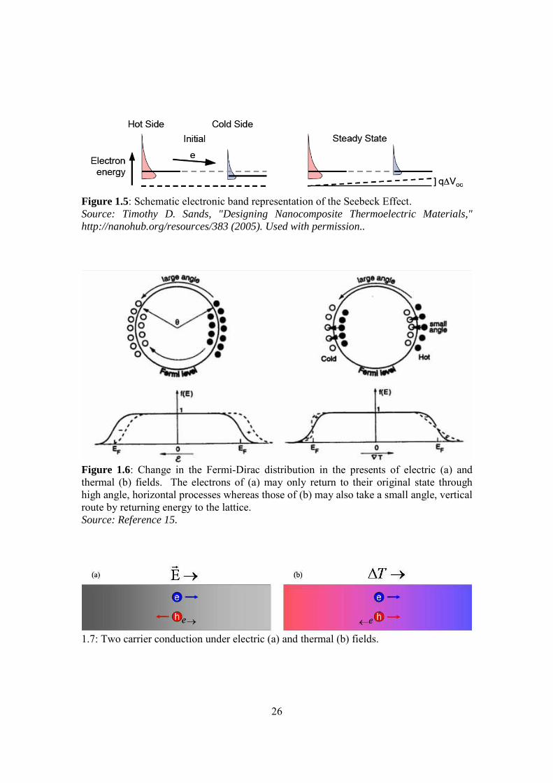
Fig. 1.6 shows the shift in the Fermi distribution of electrons due to an external
field and the reshaping of the Fermi distribution due to a temperature gradient. In the
case of an external electric field, the Fermi distribution is translated along the direction of
the electric field (Fig. 1.6a); under a thermal gradient, the exponential tail of the Fermi
distribution function is reduced on the “cold” side while it is elongated at the “hot” end
(Fig. 1.6b).
The “failure” of the Wiedemann-Franz relationship to determine the electronic
contribution to the total thermal conductivity is an important issue in thermoelectrics.
Enhancing ZT is often approached by attempting to lower the thermal conductivity while
preserving the electrical conductivity. The obvious route is to independently minimize
the lattice thermal conductivity. In order to identify and understand the effects of the
21
methods employed to do so we must calculate and remove the electronic contribution to
the total thermal conductivity.
At very low temperatures and above the Debye temperature of a material the
Wiedemann-Franz holds and the Lorenz number can be used to subtract the electronic
contribution (see Eqs. (1.22) and (1.34)):
00.1 and , D DT T L Lκ σθ θ τ τ< > ≈ ≈ (1.35)
0ph T L Tκ κ σ= − (1.36)
At temperatures in the range of D D0.1 <T<θ θ , and especially in semiconductors,
the value of L falls below that of 0L . For narrow bandgap semiconductors, the value
tends toward 2.0 or -8 -22.1 10x W KΩ . Though the value may vary a little between
different materials, it is sufficient to use -8 -20 2 10L x W K= Ω when investigating the
trends in the lattice thermal conductivity within a material system where the composition
is only changed by a few percent.
Most narrow bandgap semiconductors and semimetals have both hole and
electron bands near the Fermi energy. At higher temperatures, the interval F BE k T±
expands and more minority carriers become involved in electronic conduction. Since the
migration of holes in one direction by default mean the migration of electrons in the
opposite of another, bipolar conduction—the conduction of both holes and electrons—in
an electric field will result in a net migration of electrons in the same direction (for now
we consider only an external electric field; so, 0xT∇ = . Therefore, holes and electrons
both contribute to electronic conduction (Fig. 1.7a).

22
e hσ σ σ= + (1.37)
Under a thermal gradient with no external electric field, however, holes and
electrons compensate each other as they both migrate to the cold end (Fig. 1.7b). In the
case of holes, this can be understood by considering the hole to migrate in a random walk
fashion. Since the electrons that neighbor holes at the hot end have more thermal energy,
and thus a higher probability of ‘jumping’ to the hole than those of the cold end, holes
become ‘frozen’ at the cold end. This results in a net migration of electrons towards the
hot end. The promotion (excitation) of minority carriers at high temperatures will
inevitably result in a maximum in the Seebeck coefficient as the total Seebeck becomes a
sum of each carrier’s Seebeck weighted by its electrical conductivity and normalized by
the total electrical conductivity (when 0xT∇ = ).
e e h h
e h
α σ α σασ σ
+=+
(1.38)
There is an additional consequence of bipolar conduction that shows up in the
form of a rising tail in the total thermal conductivity where a nearly flat 1T − (for high T )
is expected. This tail comes from the electronic contribution, which is no longer just
proportional to the total electrical conductivity. The electronic thermal conductivity is
not only an addition of the individual carrier conductivities ( electronic e hκ κ κ= + ), but an
additional term known as the bipolar thermodiffusion effect term becomes significant as
Peltier-like heating occurs between different bands.16 This term is proportional to
temperature and the square of the difference between hα and eα .

23
( )2e helectronic e h h e
e h
Tσ σκ κ κ α α
σ σ= + + −
+ (1.39)
While the example has been made for the most extreme case, electrons and holes,
the truth is that bipolar conduction and diffusion may occur anytime there is more than
one band involved. The bands may only differ in dispersion and therefore effective mass.
However, the bipolar thermodiffusion effect will be most noticed in narrow bandgap
semiconductors in which valence hole bands and conduction electron bands are both near
the Fermi level and where the magnitudes of eα , hα , and h eα α− remain high while eσ
and hσ remain at least moderate.

24
Figure 1.1: α, σ, and PF plotted versus carrier concentration. Source: http://www.its.caltech.edu/~jsnyder/thermoelectrics/index.html.
Figure 1.2: Sample band structure plot. The vertical axis represents the energy of electronic states while the horizontal axis is the k-values of the electron momentum.

25
Figure 1.3: Example of an n-type semiconductor’s density of occupied states. Source: Timothy D. Sands, "Designing Nanocomposite Thermoelectric Materials," http://nanohub.org/resources/383 (2005). Used with permission.
Figure 1.4: Simplified electronic band structures of (a) metals, (b) semimetals, (c) semiconductors, (d) and insulators. In reality, there are more than just one valence and one conduction band. Also, the bands are not necessarily symmetric and parabolic.
26
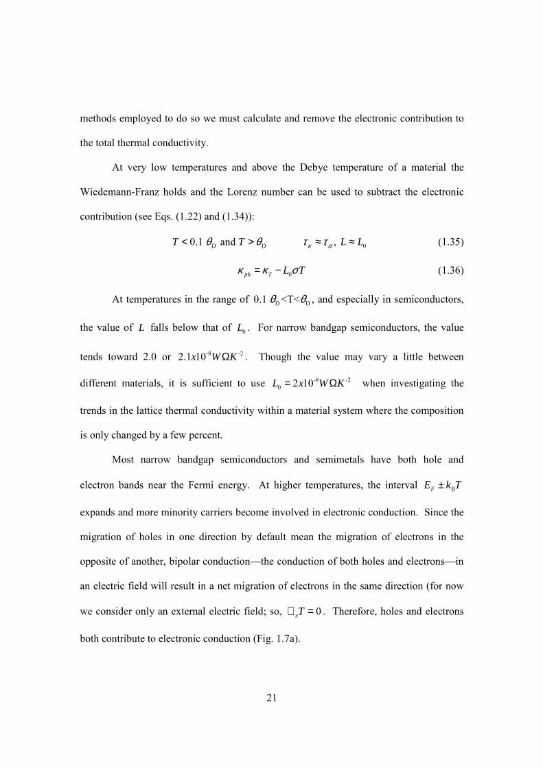
Figure 1.5: Schematic electronic band representation of the Seebeck Effect. Source: Timothy D. Sands, "Designing Nanocomposite Thermoelectric Materials," http://nanohub.org/resources/383 (2005). Used with permission..
Figure 1.6: Change in the Fermi-Dirac distribution in the presents of electric (a) and thermal (b) fields. The electrons of (a) may only return to their original state through high angle, horizontal processes whereas those of (b) may also take a small angle, vertical route by returning energy to the lattice. Source: Reference 15.
1.7: Two carrier conduction under electric (a) and thermal (b) fields.

27
CHAPTER TWO MATERIALS INTRODUCTION
Chalcogenides and Thermoelectrics
The chalcogenide group plays a special role in thermoelectrics. As discussed in
the introduction, good thermoelectric materials will be either degenerate semiconductors
or semimetals. These classes of materials are best defined by their band structure where a
degenerate semiconductor is a material with a small band gap (for thermoelectrics, a rule
of thumb is EG = 10kBT: ~0.25eV at room temperature) and contains impurity
levels/bands in the gap, whereas semimetals have of an indirect overlapping of
conduction and valance bands at different k-points. These types of materials are often
composed of at least one element from the pnictide or chalcogenide groups because it is
the difference in electronegativities between constituent elements that gives rise to
forbidden states at or near the Fermi energy and thus band gaps. Pnictogens and
chalcogens possess sufficient electronegativity values that when combined with metals or
semimetals, this criterion is met. Halogens, of course, are so electronegative that they
form ionic compounds when combined with most elements and therefore no band
structure exists. Intermetallics, on the other hand, have far too many states at and above
the Fermi energy, and are thus too metallic for thermoelectric applications.

28
Structures of Transition Metal Dichalcogenides
Transition metal dichalcogenides form a broad class of materials that contain
everything from metals to insulators (when you include oxygen as a chalcogenide). Even
in the case of titanium and the specific stoichiometry of TiX2 (dichalcogenides, where X
is a chalcogen), we can find all four classes of materials—insulator: TiO2, semiconductor:
TiS2, semimetal: TiSe2, and metal: TiTe2. Since insulators are of no value to this work
we will exclude oxides from further discussions.
Dichalcogenides of group IV and V transition metals form a layered structure that
consists of X-M-X layers separated by a van der Waals gap. These structures form
several polytypes that depend on the coordination of the chalcogen atoms within the
layers and the coordination between the layers themselves. F. R. Gamble put together a
very good paper detailing the effects of atomic radii and electronegativities on the
resulting structures for these materials.17
In terms of chalcogen-metal coordination, they may form with octahedral or
trigonal prismatic coordination (denoted with prefixes 1T- and 2H-, respectively). Fig.
2.1 shows the difference between the two coordination schemes. In the 1T and in some
2H polytypes (the 2H polytype can form two different ways depending on the interlayer
alignment), there are vacancies equidistantly positioned between the Ti atoms along the
c-axis. Gamble showed that the 2H structure with trigonal prismatic coordination is
preferred and will be adopted when the geometry of the cell due to the relative atomic
radii of the metal and chalcogen atoms permits. He further showed that the effective radii
of both constituents depend on the fractional ionic character of the bond, and by

29
definition, their differences in electronegativities. The important consequence of the
chalcogen coordination is its effect on the metal d band. For the trigonal prismatic 2H
coordination, the 2zd band is separated from the rest of the d bands as it is shifted
towards lower energies.18,19,20 Hughes and Liang19 suggest that it is the filling of this
band that determines octahedral or trigonal prismatic coordination. Yoffe21 indicated that
the 2zd band is just above EF in the 1T materials but at or just below EF in 2H
compounds. With the 2zd band resulting in a sharp peak in the density of states (DOS)
just above EF, the 1T materials will be thermoelectrically advantageous when intercalated
as EF may be raised to where the slope of the DOS is high (remembering
( )EDOS Eα ∝ ∂ ).
Fermi surfaces based on electronic structure calculations by Doran22 showed the
1T structures to have electron pockets in the shape of a column along the LML direction,
while the 2H structures have similar shaped hole pockets along AΓA (Fig. 2.2). Wilson
et al.23 implicate this unique Fermi surface geometry as evidence of the 2D nature of the
system as a layered structure. While this leads to anisotropy of the transport properties, it
may also prove useful as a mechanism for favorably decoupling the thermal and electrical
properties for optimization of the thermoelectric figure-of-merit, ZT.
Both titanium diselenide and disulfide form in the 1T polytype. Compared to the
other dichalcogenides of group IV transition metals, those of titanium form less X-M-X
bonds with a smaller fractional character. This is a result of the small atomic radii of Ti
compared to Zr and Hf.19 This, in addition to the positioning of the Ti 3d bands as a

30
result of the 1T structure, leads to a very small band gap in the case of both TiSe2 and
TiS2. Friend et al.24 reported TiS2 to be a narrow bandgap semiconductor with a bandgap
of 0.2 – 0.3 eV, and predicted TiSe2 to be a semimetal with a small, indirect overlapping
of the Ti-3d and Se-4p bands. Boehm and Isomaki determined the overlap of these bands
to be between 0.18 and 0.5 eV with angle-resolved photoemission spectroscopy
(ARPES).25 Using better angular and energetically resolved ARPES measurements,
Andersen et al. determined the overlap of the bands to be less than 0.12 eV while
resolving a spin-orbital splitting of the Se-4p orbital, which crosses EF to give rise to hole
carriers.26
Charge Density Waves
Several of the groups IV and V dichalcogenides of both 1T and 2H polytypes
undergo a periodic lattice distortion due to charge distribution rearrangement below some
temperature.23 Known as a charge density wave (CDW) state, the adoption of a
superlattice is a consequence of the unique Fermi surfaces of the materials that supports
the necessary electron-phonon interactions. In the special case of TiSe2, the CDW state is
a result of electron-hole pairing (exciton) and the subsequent interactions with the
phonons of the lattice (the so-called Overhauser type27).28 The CDW transition gives rise
to a significant peak in the Seebeck coefficient, which makes these materials at least
attractive for low temperature thermoelectric studies.43,29 On the other hand, the CDW
state generally results in a reduction of carrier concentration and, consequently, a

31
reduction in the electrical conductivity. The hope is to gain more from the increased
Seebeck than what is lost in electrical conductivity.
Intercalation
Intercalation of transition metal dichalcogenides has been widely studied, but
rarely in terms of thermoelectric applications. Yoffe’s paper21 reviewed, in general, the
effects of intercalating many atomic and molecular species into transition metal
dichalcogenides. The paper describes, in general and with some specific examples, the
effect of intercalating nitrogen hydrides, organic amines, alkali, and 3d transition metals
on the electronic properties. There have been a considerable number of efforts in
studying the ion conduction properties of Li doped transition metal dichalcogenides
where the charge transfer between the intercalants and the host layers is complete (for
example30,31,32,33). Many of these studies focused on the use of alkali intercalated
transition metal dichalcogenides as ionic conductors. Gamble et al.34 showed that by
intercalating polymers such as stearamide that the van der Waals gap may be opened
widely, resulting in an electronically 2D system where the X-M-X layers are separated by
a distance nearly ten times their thickness.
While many 3d metal intercalation studies of decades past were focused on
finding a route to high TC superconductivity, these focused on materials of the 2H and
mixed polytypic (i.e. 4H) materials where the density of states at the Fermi surface tend
to be higher.35 Only recently has superconductivity been found in an octahedrally
coordinated structure—the 1T-CuxTiSe2.36 Pure TiSe2 has even been found to exhibit a

32
pressure induced superconductivity state between 2 and 4GPa.37 These and other recent
studies of Cu intercalated TiSe2 have explored the competition between the charge
density wave and superconducting states.38,39
The Uniqueness of Titanium Diselenide
The electronic structure of TiSe2 (Fig 2.3) along with the uncommon Overhauser
type CDW transition that arises from it makes this particular transition metal
dichalcogenides a unique and interesting material for any electronic transport studies.
The small, indirect overlapping of the Ti-3d and Se-4p bands becomes increasingly
important when 3d metal intercalants occupy the octahedrally coordinated voids at (0 0
½) (Fig. 2.4). Since the indirect band overlap of the hole bands of the Se-4p orbitals at Γ
and the Ti-3d bands at L is small (<120 meV), the ratio of the electron to hole
concentration (ne/nh) is very sensitive to both the concentration of intercalants and the
number of valence electrons of the intercalants species. If all intercalants act as electron
donors to the host matrix, as Yoffe suggested,21 then more electrons per unit cell raises EF
so that fewer holes may be present until the maximum of the Se-4p band is filled. As
more recent studies show, the effect of a guest 3d intercalants on the local band structure
of the host TiSe2 matrix can be complicated and is species specific. This means the
situation becomes more than an electron counting scheme as the 3d orbitals of the
intercalants may become hybridized with those of the host Ti atoms (but to a varying
degree of hybridization).40 The charge transfer may be nearly complete, as is believed to
be the case with Cr intercalation,21 or the 3d states of the intercalants may be highly

33
localized, as is the case with Co.40 The result is a wide range tuning mechanism for
optimizing the band structure of MxTiSe2 in a thermoelectrically favorably way.
Current Thermoelectric Studies
Some researchers have made use of the relative band structures of TiSe2 and TiS2
to optimize the thermopower (Seebeck) in the ternary TiSe2-xSx.41,42 As mentioned
above, the more negative sulfur renders TiS2 a narrow bandgap semiconductor. Since the
overlap of the bands in TiSe2 is so small, substitution of only 0.1–0.3 sulfur per formula
is enough to open a bandgap in TiSe2-xSx to bring put it in the degenerate semiconductor
class in which thermoelectrics are usually found. Only one recent study published in
2009 has focused on MxTiSe2-ySy as potential thermoelectric candidate. Hor and Cava43
intercalated small amounts of Cu (x < 4%) into MxTiSe2-ySy while varying y from 0 to
0.3. This was the first study of this material where both the electronic and thermal
properties where measured so that ZT could be calculated. They found a maximum ZT of
0.07 at room temperature in Cu0.02TiSe1.7S0.3. The thermal conductivity was not reported
for the unintercalated TiSe2-xSx, leaving out an understanding of the effect of sulfur
substitution on the thermal transport. Additionally, Cu adds a large number of electrons
per unit cell, and while this may offset the number of holes favorable, it may shift the
Fermi energy past where the peak in the electronic DOS of the Ti-3d bands is positioned.
A study of the effects of intercalating other 3d transition metals, or possible a
combination of them, on the thermal and electronic transport for thermoelectric
applications is of interest by lacking.

34
Figure 2.1: Examples of 1T (a) and 2H (b and c) polytypes of the transition metal dichalcogenides. Chalcogens are represented by the green, smaller spheres. While the 1T unit cell contains only one X-M-X layer (the z=0 plane cuts through the M layer), the 2H contains two X-M-X layers. The X-M-X bonds are represented by the dashed lines.

35
Figure 2.2: Columnar hole and electron pockets in the Fermi surfaces of 2H-TaSe2 and 1T-TaS2, respectively. Reprinted from: NJ Doran, “Electronic structure and band theory of transition metal Dichalcogenides” Physica 99 (1980) 227-237, with permission from Elsevier.

36
Figure 2.3: Band structure of 1T-TiSe2. The Se-4p maximum at Γ and the Ti3-d minimum at L can both be seen crossing the Fermi energy (E = 0). Reprinted from: P Aebi, T Pillo, H Berger, and F Levy, "On the search for Fermi surface nesting in quasi-2D materials" J. Elec. Spec. Phenom. 117-118 (2001) 433-449, with permission from Elsevier.

37
Figure 2.4: Trigonal unit cell of TiSe2. Full occupation of the vacancy sites at (0 0 ½) give the NiAs structure of TiSe (s.g. P63/mmc).

38
CHAPTER THREE
TRANSPORT PROPERTIES MEASUREMENT TECHNIQUES
Low Temperature Transport
Low temperature electrical and thermal transport measurements often provide a
great deal of insight into the intrinsic character of a system. Low temperatures mean a
reduced phonon population and less thermal excitation of electrons, which, consequently,
means less phonon-phonon and phonon-electron interactions. Particularly when
temperatures are below about 10% of the Debye temperature ( Dθ ) of a material, structure
and defects (structural, magnetic, impurity, etc.) become the dominant scattering
mechanisms for both electrons and phonons.
Seebeck and Electrical Resistivity
Seebeck and electrical resistivity were simultaneously measured using a custom
designed system44 that employs the differential and traditional four-probe techniques,
respectively. Using removable chip mounts (Fig. 3.1), samples were mounted between a
copper base thermally sunk to the system and a copper pad with a heater affixed to the
transverse side using silver paint. Current input wires were soldered to the two copper
pieces while the two voltage leads for resistivity measurements were attached directly to
the sample (of length l) at about 1/3l and 2/3l. Voltage leads for Seebeck measurements
were soldered directly to the copper blocks with the assumption that the very high
thermal and electrical conductivities of copper result in no potential or thermal gradients

39
within each copper piece. The temperature difference was measured using a differential
thermocouple that was embedded into the copper blocks near the sample contact surface.
Measuring both cooling and warming curves between room temperature (~300 K)
and 10 K, the system was set to a constant cooling/heating rate of 0.25 K/min and the
sample heater was set to maintain a constant temperature difference between the two
copper blocks (and assumedly between the two ends of the sample) of about 5 K. The
low slew rate of the system allowed for a quasi-steady-state scenario where the change in
temperature that occurs during the time to complete the measurements (~1-2 sec) is very
small. A high data density was obtained by taking measurements every 120 seconds.
Quantities actually measured were voltages of the system thermocouple,
differential sample thermocouple, potential difference between copper blocks, and
potential difference between leads affixed to the sample. Tables were used to convert the
voltages of the system and differential thermocouples to obtain the system (base)
temperature and the ∆T, respectively. The measurement temperature was then taken to be
the base temp plus half the ∆T:
12measure baseT T T= + ∆ (3.1)
The Seebeck coefficient at a given temperature was simple taken to be the
voltage between the copper blocks divided by the temperature difference. Since the
copper blocks and the copper wires used to measure the voltages are at different
temperatures, this actually creates a two conductor scenario analogous with Seebeck’s
wire loop of two dissimilar metals. So, the open circuit voltage measured between the
two copper leads gives the sum of the Seebeck voltages of the copper wires and the

40
sample. The Seebeck voltage of the copper wires was calculated for the measured ∆T
and subtracted:
Cu measured measuredsample Cu
T V V
T T
αα α∆ −= = −∆ ∆
(3.2)
Since a constant ∆T was maintained across the sample, the voltage between the
resistivity leads on the sample also contains a contribution from the Seebeck effect
( ( )measured IRV V I Tα= + ∆ ). By measuring the voltage between the leads with the current
on, and then with the current reversed, the thermoelectric voltage may be removed and
the resistance of the sample between the leads may be calculated using Eq. (3.3):
( ) ( ) [ ( ) ] [ ( ) ]( ) ( )
measured measured IR IR IRV I V I V I T V I T VR
I I I I I
α α+ − + −
+ − + −
− + ∆ − + ∆= = =− −
(3.3)
Here ∆T is the temperature difference between the two leads, which is unknown.
This ∆T is not to be confused with the one measured between the copper blocks by the
differential thermal couple that is used to determine the Seebeck coefficient. Also,
Vmeasured in Eq. (3.3) is measured between leads attached directly to the sample, as
opposed to the Vmeasured in Eq. (3.2), which is measured between the leads attached
directly to the copper blocks and is used to measure the Seebeck coefficient.
Since the resistance of the sample should be independent of current and I I− += − ,
we have ( ) ( )IR IRV I V I− += − . Also, the current is measured by measuring the voltage
across a known standard resistor that is in series with sample. With the resistance of the
material between the two leads known, the electrical resistivity may be easily determined
if the sample geometry is well defined and known. Typically, the largest uncertainty in

41
determining the sample’s resistivity comes from the measurement of the sample
dimensions. Specifically, for a rectangular sample with a uniform cross-section of area,
A, and length between leads, l, the resistivity, ρ, is:
R A
lρ ⋅= (3.4)
Thermal Conductivity
Low temperature thermal conductivity was calculated from thermal conductance
data obtained from a custom designed system45 that employs the steady-state power
sweeping technique. Sample specimens used for low temperature electrical resistivity
and Seebeck measurements were also used for low temperature thermal conductivity
measurements so that the uncertainty of the sample’s cross sectional area would cancel
out when ZT, Eq. (1.1), is calculated. Samples were mounted on commercial pucks
designed by Quantum Design for their PPMS® system’s AC Transport option. The
pucks were modified for thermal conductivity measurements (Fig. 3.2) and used in a
custom built, cryocooler system that measured thermal conductance from 10 to 300 K.
The system and technique is described in detail in reference 45.
The following equation was used to calculate the thermal conductivity, κ, from
the thermal conductance, K, the cross-sectional area, A, and the length, l, between the two
junctions of a differential thermal couple used to measure the ∆T between two points of
the sample:
K A
lκ ⋅= (3.5)

42
The thermal conductance of the section of the sample between the two points
where ∆T is measured, K, was determined at each temperature by the steady-state
equation: P K T= ∆ , where P is the heating power input into the sample. By measuring
the temperature difference of the differential thermocouple and the heating power input in
the sample for a range of heating powers, K may be determined as the slope of P vs ∆T.
The base temperature was stabilized to within +/- 30 mK of the set temperature before
any data acquisition was taken. This stability of +/- 30 mK was maintained throughout
the entire measurement sequence at each temperature set-point. Once a steady-state
condition was reached, the current input into the heater was calculated from a measured
voltage drop across a standard resistor in series with the heater, and the electrical power
input into the heater was calculated from P=I2R. Since the nominal value of the heater
resistance was not nearly precise enough for this calculation, the resistance was
determined using Ohm’s law and the voltage drop across the heater was measured for
each calculation of the power using a four probe configuration at the sample puck. Since
thermal loss through conduction along leads must be minimized, only two leads ran from
the heater to the sample puck, and then four wires from the puck to the measurement
panel. The small error arising from voltage drops along the two leads from the puck to
heater has been determined and is accounted for in calculations of the heater power.
The heating power input into the sample was therefore calculated as the corrected
electrical power input into the heater minus any thermal loss terms
( 2sample heater lossP I R P= − ). The loss terms were minimized by using small diameter (.004”)
phosphor bronze (κPB ~ 70 Wm-1K-1 at 300 K, compared to κCu ~ 400 Wm-1K-1) leads to

43
the heater in order to minimize loss through conduction. The differential thermocouples
were made using .001” constantan-chromel-constantan whose small diameter and
relatively low thermal conductivity (both: κ ~ 20 Wm-1K-1 at 300 K) result in a very low
thermal conductance. In order to accurately measure the ∆T of sample, two 38 AWG
copper wires coated with enamel insulation were affixed to the sample perpendicular to
the length at two points using Stycast®. The insulation on outer side of the wires is then
removed to expose the copper to which the junctions of the thermocouple are soldered to
achieve maximum thermal contact while keeping the thermocouple electrically insulated
from the sample.
An additional source of power loss is through radiation from the sample, heater,
and wires. This radiative loss term starts to become a concern typically above T ≈ 200K.
The rate of radiative heat transfer between an object and its surroundings depends on the
surface area and emissivity of the object (sample) and the temperature difference between
the object and its surroundings according to the Stefan Boltzmann law (actually the
difference in the fourth power of the temperatures). Besides minimizing the heat
conduction through the wire leads to minimize the heat available for radiation, a copper
cap was placed over the puck in thermal contact with the system base to introduce a
surrounding that minimizes the temperature difference. Additionally, the cap was gold
plated on the inside to provide a reflective coating to reflect the radiation back to the
sample.
Because the surface area should be minimized, the dimensions should be chosen
to reduce the surface area relative to thermal conductance (which is directly proportional

44
to the cross-section). Since the surface area is directly proportional to length while the
thermal conductance is inversely proportional to length, a very short, fat sample would be
preferred. However, since a thermal gradient must be established and a ∆T measured
between two points whose separation must be measured, a minimum length of at least 4-6
mm is needed. To maximize the cross-sectional area while minimizing the surfaces area
for a sample of a given length, the cross-section ought to be square.
Although a short sample with a large cross-section is preferred for thermal
conductivity measurements, the opposite is true for electrical resistivity measurements.
The length should be maximized to allow for creating a so that the separation between the
voltage leads may be maximized since the resistance, and thus the voltage that arises
from Ohm’s law, is maximized. This is simply an issue of signal-to-noise ratio. A small
cross-section if favorable for two reasons; the first being that the resistance is inversely
proportional to the cross-section, and the second is that a uniform current density at and
between the resistivity voltage leads is necessary. Tritt suggests placing the leads no
closer than the width of the sample (assuming square cross-section) from the ends, where
the current is input.46
Since the Seebeck coefficient is measured simultaneously with electrical
resistivity, maximizing the length makes creating a sufficient ∆T possible within the
limitations of the heater power and sample thermal conductivity. A sufficient ∆T will
result in a Seebeck voltage that is large enough to be accurately measured against the
inherent signal noise and voltmeter capabilities.

45
When calculating ZT, it is essential to use transport data all measured on the same
sample and along the same direction. This will ensure that the ZT is indeed
representative of the specimen, as-is, with all defects, texturing, anisotropy, etc. included.
Additionally, since the dimensions go into the calculations of both the electrical and
thermal conductivities in the same way, the uncertainties in sample cross sectional area
will cancel as the ratio becomes a ratio of conductances instead of conductivities in ZT.
The lengths that are used for resistivity and thermal conductivity are typically not exactly
the same so they do not cancel. To balance requirements on the sample dimensions
between electrical and thermal transport measurements, samples were cut out of the
center of a densified, polycrystalline pellet of about 2 mm thick to be 2 mm wide and 6-8
mm long. Both the voltage leads for resistivity measurements and the copper rails for
thermocouple fixing were placed at about 2-2.5 mm from either end.
Hall Coefficient
As discussed in the first chapter, the thermoelectric power factor ( 2PF Tα σ= )
may be maximized at some carrier concentration. It is therefore useful to determine the
carrier concentration via of the Hall Effect.
In 1879, Edwin Hall first made quantitative measurements of the deflection of
current due to a magnetic field by driving a current through a rectangular section of gold
foil placed in a magnetic field perpendicular to the face of the foil and then measuring the
transverse voltage.47 Because at the time the electron was yet to be discovered, the best
that Hall could do in terms of modeling was to not that the voltage produced is directly

46
proportional to the product of the magnetic field strength and the primary current. In
1904, Henrik Lorentz correctly derived the force, Fr
, that describes the reaction of a
particle with a charge q traveling with a velocity, vr , in a magnetic field, Br
:48
F qv B= ×r rr (3.6)
This magnetic force will be balanced by the electrostatic force ( F eE=r r
) that
arises from the deflected electrons ‘piling’ up at one of the material. Writing the electric
field in terms of the potential difference divided by the distance and the velocity of Eq.
(3.6) in terms of the current, I, and then equating the two forces gives a result for the
voltage that arises due to the Hall effect in terms of the thickness of the material, d, and
the carrier concentration, n:
H
IBV
ned= H
IBV
ned= (3.7)
In general one must use and average of 4 voltages [(+I, +B), (-I, +B), (-I, -B), (+I,
-B)] in order to cancel out all the thermal contributions, such and thermoelectric, Nerst
effect and Ettinghausen effect, etc.). We use with the PPMS an ac current and reverse the
field and average to get the correct Hall voltage.
Fig. 3.3a schematically shows the Hall effect on a stream of electrons
characterized by a current I passing through a thin slab of a material of thickness d in a
magnetic field of strength B. Eq. (3.7) is only valid when the voltage is measured
between two points that fall on a line perpendicular to the flow of current, which must be
uniformly distributed through the cross-section of the sample. If the two voltage leads

47
are not attached perfectly perpendicular to the current, then an additional voltage will
arise from Ohm’s law.
The left side of Fig. 3.3b depicts a three probe configuration (five if you include
the current leads) where the positive lead for the Hall voltage is replaced by two leads
attached at points that are collinear with a line parallel to the flow of current. These two
leads are connected to the opposite ends of a high precision potentiometer. The center
tap of the potentiometer is then used as the positive lead of the Hall voltage. If the
potentiometer is balanced so that the voltage is zero when the magnetic field is zero,
regardless of the driving current, then any voltage that arises must be strictly due to the
Hall effect.
The Hall coefficient was measured on a few select samples to probe the carrier
concentration as a function of nickel concentration in NixTi1+δSe2. Using the
configuration depicted in Fig. 3.3b, the Hall voltage was measured as the magnetic field
was swept from -0.5 Tesla to +0.5 Tesla while the temperature and current remained
constant. The slope of VH versus B is then I/(ned). The effective carrier concentration
was readily obtained from the slope. This was repeated for several temperatures in the
range of 100 – 300 K.
It is important to note that this is the effective carrier concentration as it is an
average of the hole and electron concentrations (p and n, respectively) weighted by each
carrier’s mobility (µp and µn).49
( ) ( )2 2
2 2 2h e
effh e
p n p nn
p n p n
µ µ βµ µ β
+ += =
− −, where e
h
µβµ
= (3.8)

48
Specific Heat Capacity
Low temperature specific heat capacity may provide several important pieces of
information about a sample. When the data is taken up to room temperature, the shape
may indicate that where the Dulong-Petit value of cv becomes valid. Above the
temperatures where cp becomes a linear function of T, the cv saturates at the Dulong-Petit
limit. So, if the cp of a sample is beginning to become linear just below 300 K, it is
appropriate to assume that the cv has saturated above 100°C (~373 K).
Since both the ions in the lattice and the electrons associated with those ions may
store heat, the total heat capacity of a system will have at least two terms. The heat
stored in the vibrational modes of the ions (phonons) has been most accurately modeled
by Peter Debye.50 His approach was to associate the vibrational modes of the lattice to
phonon wave energies and then to use Bose-Einstein statistics to obtain the total energy
of all phonon modes.
4 3
3 0
91
DT TB
xD
Nk T xU dx
T e=
−∫ (3.9)
By differentiating the total energy with respect to temperature, Debye arrived at
an equation for the phononic heat capacity that provided a very good fit to the
experimental data of insulators over all temperatures:51
3 4
20
9( 1)
D T x
V B xD
U T x eC Nk dx
T e
θ
θ ∂= = ∂ −
∫ (3.10)
The phononic heat capacity therefore depends on the temperature, T, the total
number of atoms, N, and a parameter known as the Debye temperature, θD. The Debye

49
temperature is a collection of universal and material specific constants, such as Planck’s
constant, h, the Boltzmann constant, kB, the velocity of sound in the material, vs, and the
number of atoms per unit volume, N/V:
1
31 62
sD
B
hv N
k Vθ
π =
(3.11)
In the limit of DT θ>> , the integral of Eq. (3.9) may be simplified by the
approximation 1xe x≈ + . This results in 3V BC Nk= —the classical Dulong-Petit limit.
In the low temperature limit, where DT θ<< , an approximation may be made to the
integral in Eq. (3.9) that results in a simplified low temperature phononic heat capacity—
Eq. (3.12). The accuracy of Eq. (3.12) to predict the heat capacity of materials below 5 –
8 K was the great success of Debye’s model.
4
33
125
BV
D
NkC T
πθ
= (3.12)
When electrons are no longer localized to an ion core, they may store and
transport heat independently of the lattice. From Chapter 1, Eq. (1.32) gives the
electronic contribution to the heat capacity and the total heat capacity of conducting
materials at low temperatures is:
2 2 4
33
121 2 5
B BV
F D
n k NkC T T
E
π πθ
= + (3.13)
From Eq. (3.13) it can be seen that low temperature (below 5 K) cp data may be fit
with a linear plus a cubed term, and the coefficients may be used to determine the Fermi
energy and Debye temperature of the system. The fact that cp is measured instead of cv is

50
of no consequence as cp≈cv at low temperatures. Knowing EF and θD can be useful as the
latter may be used to calculate the velocity of sound, to which the lattice thermal
conductivity is related, and EF has much to do with electronic transport.
The specific heat at a constant pressure was measured on a Quantum Design
PPMS® system from 1.7 to 300 K at the National Institute for Standards and Technology
by Dr. Yonggao Yan. The heat capacity was determined for each sample by the
relaxation method52 where heat is input into the sample stage (and sample, when present)
for a time and then shut off. The temperature of the platform is measured with a
Cernox® thermometer as a function of time and the total heat capacity of the stage and
sample (plus any thermal contact media used, such as grease) is determined by the time it
required for the temperature to reach the initial temperature. Determining the sample
heat capacity therefore involved measuring an addendum of the stage and thermal contact
grease. EF and θD were subsequently determined for all samples with cp’s measured.
High Temperature Transport
Seebeck and Electrical Resistivity
The Seebeck coefficient and resistivity were measure simultaneously with the
commercial ZEM-2 system from ULVAC Technologies, Inc. Measurements were taken
from 50°C to 300°C. While the sample stability and the capabilities of the ZEM-2 would
allow for measurements up to at least 500°C, data was taken only to 300°C because the
Seebeck coefficients and thus the ZT’s of the samples reach a maximum between 200 and

51
300°C due to bipolar conduction. A high density of data points was not necessary in the
temperature range measured as no sharp features were expected in the data. This fact, in
addition to data density being proportional to the time required to obtain the data, resulted
in data being taken every 50°C.
Like the low temperature systems, the ZEM-2 employs the four-probe technique
for measuring electrical resistivity. Unlike the former, the ZEM-2 utilizes mechanical
springs to make pressure contacts of the current input posts and the voltage leads.
Additionally, the voltage leads themselves are of a different nature. The ZEM-2 uses a
method where each lead is actually a thermocouple rather than a single wire. The
thermocouple junction is located just outside the end of a two-bore ceramic tube that
houses the thermocouple’s leads, and is mechanically pressed to the side of the sample to
give good thermal and electrical contact. The advantage of this method is that both the
temperature and electric potential may be probed at the point of contact. As two such
thermocouple probes are aligned vertically along the sample, the two temperatures (T1
and T2) of their points of contact may be measured to obtain ∆T while measuring the
potential difference between the negative leads of each thermocouple will yield both the
Seebeck voltage (when I=0) and the voltage due to Ohm’s law (plus Seebeck, when
I≠0)—Fig. 3.4.
The sequence used for measurements involved stabilizing the system at a base
temperature and then raising the temperature of the lower arm of the probe to achieve a
temperature gradient across the sample. Once the ∆T is stabilized, the voltages of each
probe thermocouple as well as the voltage between the negative leads of each

52
thermocouple are measured with the current off, and then with the current on. The
system will persistently make measurements at an interval of about once every few
seconds while tracking the latest three data points. Once the standard deviation of the
most recent three measurements is low enough, the average will be recorded and the
system moves to a higher ∆T to repeat stabilization and measurement. The ∆T set-points
used were 5, 10, and 15°C above each base temperature.
The raw data is recorded in a tab delimited text file that must by analyzed by an
addition program. The raw data contains one line per each T+∆T measured with the
following columns: T (TTC1, see Fig. 3.4), ∆T (TTC2-TTC1), ρ (sample resistivity at T+∆T),
αwire (tabulated Seebeck of negative lead of thermocouple at ∆T), and ∆DC (Vα). The
analysis software will calculate one Seebeck coefficient and resistivity value for each
base temperature set (meaning T + [∆T=5, 10, 15°C]. Both T and ρ are simply averaged
from the set. The Seebeck voltages (Vα) must first be corrected by addition of the
contribution of the thermocouple leads ( [ ] , ,a b a b sample measured wireV V V V V Tα α α+ = − → = + ∆ ).
The Seebeck coefficient is then calculated from the slope of the corrected Seebeck
voltage versus ∆T:
( ), vs. sample sampleslope V Tαα = ∆ (3.14)
Fig. 3.5 schematically shows the ZEM-2 probe configuration. The system
temperature is measured by a thermocouple that is inserted into a metal sheath that
encloses the parts shown in the figure (base thermocouple and sheath are now shown).
This thermocouple is used to measure the base temperature, which is controlled by six
halogen lamps at the focal point of six curved reflecting surfaces surrounding the probe.

53
Once the base temperature is stabilized, the platinum heater located in the lower arm of
the probe is used to achieve a temperature difference across the sample. This ∆T is
measured by thermocouples located in upper and lower probe arms, and as such, the
actual ∆T between the sample thermocouples used for measuring Seebeck and resistivity
will be lower.
Thermal Conductivity and Diffusivity
Due to the high level of radiation loss that comes with high temperature thermal
conductance measurements, the thermal conductivity was not measured directly above
room temperature. Instead, the total thermal conductivity above room temperature was
calculated from the mass density (ρD), specific heat (cv), and thermal diffusivity (D):
D vc Dκ ρ= (3.15)
The density was measured using Archimedes’ principle where the buoyancy force
of the samples submerged in water was determined and used to calculate the volume. Eq.
(3.15) requires the specific heat at a constant volume, which is much more difficult to
measure than the specific heat at a constant pressure (cp). In instances where the high
temperature thermal conductivity was calculated, the Dulong-Petit limit53 (cD-P) of the
specific heat capacity at a constant volume (cv) was used. The Dulong-Petit law restricts
the maximum value of cv to 3kB per atom.54 This results in 3 / . .vc aR f w= where cv is in
units of J·°C/g, a is the number of atoms per formula, R is the ideal gas constant, and f.w.
is the formula weight. Unless there is a structural or electronic transition above room

54
temperature, cv ought to approach and saturate at the value of cD-P. As differential
scanning calorimetry curves show no such transitions, the Dulong-Petit limit is thought to
be valid for high temperature calculations of the thermal conductivity.
A Netzsch LFA 457 MicroFlash system was used to measure the thermal
diffusivity on a few select samples. This system pulses a laser on the bottom of the
sample and then measures the temperature profile of the top as a function of time with an
infrared detector. The calculation of the diffusivity of the material comes from
measuring the half-time of the rise and saturation of the infrared detector signal. By
solving the 1-D heat flow equation using Fourier analysis and the boundary conditions of
the sample geometry, the thermal diffusivity may be determined from the half-time of the
signal rise, from a relationship known as the Parker equation:55
2
1/2
0.138785 LD
t= (3.16)
Because the initial goal of this project was to probe the low temperature
thermoelectric properties, most samples were cut for the low temperature measurements
before running high temperature thermal analysis, which requires the whole pellet.
Differential Scanning Calorimetry
A very useful tool for thermal analysis of a material is differential scanning
calorimetry (DSC). This technique uses the relationship between heat exchange,
temperature, and the total heat capacity of a material to probe many types of structural
and other transitions that affect the specific heat capacity of a material. Glass transitions,

55
solid-solid phase transitions, partial or full melting, degassing, etc. may all give
signatures in a DSC curve. This may be used to determine melting points, sample purity,
decomposition temperature, and when the signal is calibrated using a standard, cp.
DSC curves were measured on a few select samples on a Netzsch Pegasus 404 C.
This system uses a platinum stage that accommodates two small crucibles. The crucibles
are platinum with alumina liners and platinum lids. On the underside of the stage,
beneath each crucible, one junction of a differential thermocouple is attached. When the
two points of contact with the stage (beneath each crucible) are isothermal, the signal
from the differential thermocouple leads will be zero. As heat is evenly input into the
system at a constant rate, the difference in total thermal capacities of the contents of the
two crucibles will result in a difference in their temperatures and thus a DSC signal.
The nature of this method of analysis is so sensitive that differences in the two
sides of the stage as well as in the two crucibles must be accounted for. For this reason a
baseline is often measured (always in the case of determining cp). For determining
sample stability (i.e. looking to exclude the occurrence of decomposition or melting up to
a particular temperature) a baseline is not necessary as only the shape of the DSC curve is
relevant.

56
Figure 3.1: Removable sample mounts for low temperature resistivity and Seebeck coefficient measurements. Source: See reference 44.

57
Figure 3.2: Thermal conductivity measurement sample mount. Source: See reference 45.

58
Figure 3.3a: Deflection of electrons moving in a magnetic field give rise to the Hall voltage, VH.
Figure 3.3b: Hall effect measurement schematic. For a homogeneous sample, the potential at the spatial center between the +VA and +VB leads can be found by adjusting a potentiometer in the configuration shown in the figure on the right so that the potential difference between –V and the center tap of the potentiometer is zero when the magnetic field is turned off.

59
Figure 3.4: ZEM-2 probe sample thermocouple arrangement with signals measured and their interpretations.
Figure 3.5: ZEM-2 probe schematic. The upper and lower arms of the probe are movable in the vertical position and are used to hold the sample. The platinum resistance heater is used to reach the ∆T set-points as measured by the upper and lower thermocouples. Probe thermocouples in contact with the side of the sample are used for measuring Seebeck and resistivity. The base temperature is measured with an external thermocouple attached to a metal sheath (not shown) that covers the apparatus shown and is supported by the ceramic rails at the top of the image.

60
CHAPTER FOUR
SAMPLE SYNTHESIS AND PROCESSING
Sample Synthesis
All samples were synthesized by mixing raw elemental powders in stoichiometric
proportions inside of a quartz tube. Table 4.1 contains the details of the powders used in
sample synthesis. Because of the propensity of copper to oxidize, the Cu powders were
first etched in dilute HCl and then rinsed with distilled water and then alcohol. The tubes
were subsequently evacuated to below 30 mTorr and then sealed using a hydrogen torch.
The sealed tubes were placed, upright, into bench-top muffle furnaces with
programmable temperature controllers. All samples were synthesized using the same
temperature program (Table 4.2), with a reaction temperature of 650°C and a final hold
time of 5 days.
Material Manufacturer Purity Form/Particle Size
Ni Alfa Aesar Puratronics 99.996% Powder -120 Mesh
Cu Alfa Aesar 99.5% Powder -100 Mesh
Ti Strem 99.5% Powder -325 Mesh
Ta Alfa Aesar 99.96% Powder -60 Mesh
Se Alfa Aesar 99.9% Powder -325 Mesh
S Alfa Aesar Puratronics 99.999% Pieces ~2-3 mm Table 4.1: Elemental suppliers, purities, and sizes.

61
Step Set Point (°C) Rate (°C/hour) Duration (hours)
Initial Ramp 500 125 4
Preliminary Hold 500 N/A 12
Final Ramp 650 50 3
Final Hold 650 N/A 120 Table 4.2: Sample synthesis parameters.
Based on the work of Hor and Cava43 (see Chapter 2) the first samples
synthesized were Cu0.02TaSe1.8S0.2 (XCh100) and Ni0.02TiSe1.8S0.2 (XCh101). The goal
with the latter was to switch Cu (one of Hor and Cava’s best samples was
Cu0.02TiSe1.8S0.2) with Ni to see the effects of other 3d intercalants on electronic transport.
Intercalating Cu into sulfur substituted TaSe2 was more or less a venture of curiosity.
Initial transport measurements resulted in the project focusing on TiSe2-based
compounds. Initially, the ratio of Se to S was varies for a constant 2% Ni per formula.
While the properties of the Ni intercalated samples (XCh111-114) were improved over
Hor and Cava’s Cu doped samples, it was necessary to attempt to understand the role of
the nickel intercalant. Therefore, a series of samples with varying amounts of Ni
intercalated into TiSe2 was prepared (XCh115-126). Finally, samples were prepared and
processed under different conditions to see the effects of the processing on the structure
and transport properties (XCh127-129; XCh130-132 are divisions of the former that were
processed at different temperatures).

62
Table 4.3: Samples list with nominal compositions. Samples are referred to as XCh[num], where [num] is the sample number. The sample number is sequential and follows chronologically the order of synthesis. The samples are grouped in terms of relevant compositions and investigation goals.
Processing
All samples were densified using spark plasma sintering (SPS). Like hot
pressing, the SPS process uses uni-axial loading in a high temperature environment to
compact powders and induce grain inter-growth to form a solid pellet. The main
difference between the two processes is in the source and nature of the heating. In spark
plasma sintering, the sample itself is the source of the heat as current driven through the
sample causes joule heating at the grain boundaries, which is contrary to a hot press
where the sample is externally heated by a large graphite element that surrounds the die
and punches that contain the sample.
The current supplied to the sample was rectified into a pulsed direct current. The
system, being able to control the output in terms of alternating between on for a number
of pulses and then off for a number of pulses in a sort of gating fashion, was set to on for
63
12 pulses and off for 2 pulses. The reason for using a pulsing direct current instead of a
regulated one has to do with maximizing the arcing action that is the signature of the SPS
process. The purpose of using an alternating on-off gating action is to allow for the
system to have some sort of relaxation time to prevent overheating.
The nature of the heating in spark plasma sintering comes with both advantages
and disadvantages. The most obvious advantages of internally heating the sample are
higher ramping rates, greater control of the sample temperature, and reduced processing
time. The processing time of the SPS is reduced over the hot press (usually
20%SPS HPt t≈ ) since the entire chamber is not heated in the SPS and therefore the thermal
mass of what is actually heated, and then cooled, is much lower. The higher heating rates
result in a greater preservation of the microstructure as less time is spent at lower
temperatures where surface diffusion dominates over bulk diffusion.56 Preserving small
grain size or unique and complex microstructures is often advantageous for
thermoelectrics as they are often effective in suppressing the lattice thermal conductivity
in a material. Because of the SPS process’ greater efficiency in initial neck formation by
grain boundary pre-wetting and then in promoting densification via crystal diffusion (due
to the localized heating), the pressures involved SPS processing are lower than those
required for hot pressing—typically, 25%SPS HPP P≈ .
One possible consequence of the electric field used in the SPS process is
electromigration. This is a result of momentum being transferred from the current
carriers to the ions of the conductor, which in the case of SPS, is the sample.57 This
effect is not necessarily a concern to this work because the rate of electromigration

64
depends on the current density, activation energy of ions. While the current densities
used in this work were high (200 – 400 A/cm2—not taking pores into account), this is an
order of magnitude lower than, for example, those used in the experiments of reference
57. Additionally, the time scale involved with electromigration is generally on the order
of days, if not weeks, compared to just minutes for this work. These comparisons
considered, the possibility of electromigration in the processing of all samples in this
work was ignored.
The processing of all samples began with grinding the precursor powders using an
agate mortar and pestle. Each sample was removed from the sealed quartz tube in which
it was synthesized, ground, and loaded into a die for SPS processing within a time frame
of one to two hours. This was done to minimize any oxidation of the powders. The dies
were ½” inside diameter and made out of graphite, as were the punches. A small hole
was drilled into the side of each die at half the height and just deep enough so that the
distance from the end of the bore to the inside wall of the die was about 1-2 mm. This
hole accommodates the thermocouple of the system that is used to monitor the processing
temperature.
The processing parameters were initially controlled manually throughout the
duration of the sintering process in order to determine the appropriate temperature and
force. The force (actually the pressure, which depends on the diameter of the die to
which the force is applied) is not as critical for most samples when processing with SPS
compared to HP. Generally, 30 to 50 MPa is sufficient, but the only way to know the
appropriate force is through trial and error. If the sample does not begin sintering, or

65
does not sinter enough before the temperature of processing reaches near the
decomposition or melting point of the material, then the pressure must be increased.
Simply using a very high pressure for all samples is not favorable as the load is not
isostatic and therefore a higher pressure means a higher possibility of texturing that
would result in anisotropy in the transport and mechanical properties.
While the force is set in the beginning of the process and remains constant, the
temperature is actively controlled throughout the process by adjusting the current limiting
knob. Monitoring the z-axis position (z) of the rams is key to determining the
temperature at which sintering begins and saturates. The initial ramping targets a heating
rate of 300 – 400 °C/min, and as the die (sample, die and punches, actually) begins to
heat up, the z will first drop as to maintain constant force as it compensates the thermal
expansion of the system. Once the temperature reaches roughly 60% of the
decomposition or melting limit of the material, the rate was slowed to about 100 – 200
°C/min until the z begins to increase. At this point the temperature is allowed to rise an
additional 5-10% and then held constant. The duration of the hold time is determined by
the travel of z—once it begins to level off, the process is then deemed to be finished.
The first sample to be densified was XCh100 (Cu0.02TaSe1.8S0.2). The force was
set to 5.3 kN, which results in ~50 MPa when applied to the ½” (inside) diameter dies
that were used for all samples. The temperature was increased as described in the
previous paragraph until the z began to increase as the sample began to sinter and
compact—near 730 – 750°C. The hold temperature was maintained at 800°C for about 6
– 8 minutes. The second sample, XCh101 (Ni0.02TiSe1.8S0.2), was likewise processed

66
with roughly the same parameters. Both samples came out of the dies as solid pellets
without cracks. Even after samples were cut for measurements, they appeared to be
macroscopically homogenous and without visible defects. As the processing was
assumed to be successful, and to ensure consistency of processing dependent effects
between all samples, a temperature program was set for all samples (Table 4.4). Using
the programmable temperature controller allowed for further maximization of the initial
heating rate.
Step Set Point (°C) Rate (°C/min) Duration (minutes)
Initial Ramp 600 600 1
Approach Sintering 750 150 1
Approach Hold 800 50 1
Hold 800 0 6 Table 4.4: Automated temperature program used for all samples XCh102 through XCh126, except XCh109.
For reasons explained in the following chapter, samples XCh127 through XCh132
were synthesized with the intention of looking at the effects of different processing
temperatures on the final composition, structure, and subsequent transport properties.
Samples XCh127-130 were processed with a similar program as described in Table 4.4
with a final hold temperature of 650°C and duration of 6 minutes. Samples XCh131-132
where likewise processed with a final hold temperature of 725°C for 6 minutes.

67
CHAPTER FIVE
STRUCTURAL AND COMPOSITIONAL ANALYSIS
Structure Analysis Using X-ray Diffraction
The initial phase analysis performed between synthesis and densification was
performed with a bench-top X-ray diffractometer (Rigaku MiniFlex). Synthesized
powders were ground using an agate mortar and pestle to maximize the random sampling
of crystallite orientations. Cu-kα radiation was used which included both kα1 and kα2
wavelengths. Using a two-theta goniometer, data was collected in 0.01° steps with a scan
rate of 1.0°/min.
These initial XRD scans showed the samples with no Ni to be single phase (TiSe2,
spacegroup 3 1P m ). In all samples that contained Ni, there were peaks indicating a
secondary phase of NiSe2. The relative intensities of these peaks increased with
increasing Ni content and the area fraction of the strongest NiSe2 peak to the strongest
TiSe2 peak of XCh118 (~5% Ni) was roughly 4%, suggesting that most of the Ni simply
formed NiSe2 during synthesis rather than going into the TiSe2 matrix as an intercalant.
Since most references indicate that a several step process was necessary for reaching a
homogeneous intercalated phase, this should be expected. The surprising result of the
SPS process, as shown in Fig. 5.1, is that it removed all observable traces of the
secondary phase. A look at the shift in the (002) peak towards higher 2θ and the
broadening of the (110) peak after SPS indicate that the Ni does go from the secondary
phase to the vacancies in the van der Waals gap of the host TiSe2 matrix.

68
Table 5.1: Comparison of before and after SPS processing XRD data. The table above contains data for XCh115 while the lower table is of XCh118.
Pieces cut from spark plasma sintered pellets were also ground and sent to the
University of Waterloo for high resolution X-ray analysis by Dr. Holger Kleinke’s group.
Obtaining high resolution data was necessary for refining the structure parameters.
Diffraction patterns were obtained with monochromated Cu-kα1 radiation using an INEL
XRG 3000 diffractometer equipped with a position-sensitive detector. Data was

69
collected from 2θ = 8 to 118° with a bin-width of .029°. Since a position sensitive
detector collects counts from the full range simultaneously, it is the collection time that
contributes the fidelity of the pattern rather than a scan rate—the count time for the high
resolution patters was 18 to 20 hours. While the bin-width of the high resolution data is
larger than that of the bench-top Rigaku system, the short sample-to-detector distance of
the Rigaku system is roughly half that of the INEL system, and the surface area of the
Rigaku detector is also larger than that of the INEL detector. These two differences
result in the Rigaku detector being less spatially resolved as it covers a greater portion of
the solid angle. Additionally, the combination of the Rigaku’s scan rate and step size
results in a count time of 0.6 seconds per step. This is far lower than the 18 to 20 hours
of counting for all angles with the INEL system.
The XRD patterns taken with the INEL system were indeed much smoother than
those taken with the Rigaku system. The background was easily fitted and removed, and
then the peak profiles fitted. Most peaks were easily profiled with the exception of the
peak located near 2θ=14.5° for all samples. In the TiSe2 phase, this peak corresponds to
the (001) planes. Figure 5.2a shows the (001) peak of sample XCh115. As seen, the
peak profile is not well profiled using just one peak. Using the MDI Jade software
package, the peaks were deconvoluted (Table 5.4). Since only the (001) peak is not fitted
well with one peak, it is unlikely that a separate phase exist on a macroscopic level—as
in separate crystallites. It is more likely that the effect of having both Ni and Ti in the
vacancies between a-b layers results in an order-disorder scenario where layers may
appear ‘corrugated’ or ‘dimpled’. This effect may not be apparent in higher reflections

70
across multiple planes because the range of the order-disorder is small enough that it is
lost in the added broadening that naturally comes with higher reflections. That is to say,
that the (002) peak may be a convolution of two peaks which are both broad and centered
closer together so that they can be fit as one peak.
Table 5.2 displays the c and a lattice parameters calculated from the high
resolution XRD patters. The c lattice parameter was calculated by doubling the d-spacing
determined from the (002), and also by doubling the difference between (001) and (002).
The latter method is used to negate any possible offset in 2θ. In a like manner, the a
lattice parameter was calculated from the difference of the (100) and (300) peaks. A
factor of 3/2 comes from the fact that (300) plane spacing is 1/3 that of (100) as a result
of being in reciprocal space, and a factor of 2/√3 (=1/sin[60]) arises from the trigonal
shape of the unit cell. From samples XCh115 to XCh119 both the c and a lattice
parameters increase with both increasing Ni and decreasing Ti. Sample XCh118 does not
necessarily follow this trend, but as it is shown in the later chapters, this sample also
breaks trends in some transport and other physical properties.
The apparent trend itself is somewhat surprising. While studies of Ni
intercalation show a trend of decreasing c with increasing Ni (up to at least x = .25),61
quantitative studies of the effect of excess Ti on the lattice parameters are lacking.
However, if all the vacancy sites of the van der Waals gap are filled with Ti, then the
structure becomes TiSe which have the lattice parameters c = 6.301 Å and a = 3.571 Å.
The TiSe structure preserves the octahedral coordination of the Se and Ti but now forms
a three dimensional structure with no van der Waals gap. The c and a are expanded as

71
the Ti atoms at z = 0 are hybridized with those at z = 1/2 and their covalent radii must be
accommodated. Subsequently one should expect the c lattice parameter to expand with
increasing excess Ti. The observed trend does not follow what is expected for either the
Ni or the excess Ti. It may be perhaps that Ni + Ti in the van der Waals gap has a unique
effect on the lattice at relatively low concentrations, but as the Ni content increases while
the excess Ti decreases, the c parameter will begin to follow the trend of decreasing with
the increasing Ni.
Table 5.2: Lattice parameters calculated from high resolution XRD data. The c parameter was calculated two ways: as double the difference between the d-spacing of the (001) and (002) peaks, and as double the d-spacing of the (002) peak. The amount of Ni and excess Titanium were determined from EPMA (see next section: Compositional Analysis).
Table 5.3: d-spacing of several peaks for all samples measured. Here the (001) peak has not been deconvoluted so the d-spacings are a result of the best fit using single peaks.

72
Table 5.4: Deconvolution of the (001) peak from high resolution XRD data. The separation (in 2θ) of deconvoluted peaks increases with Ni concentration.
Table 5.5: The trend of increasing secondary (001) peak d-spacing roughly correlates to both increasing nickel and decreasing excess titanium content.
Due to sample throughput limitations of the high resolution XRD at the
University of Waterloo, only a few samples could be analyzed with high resolution XRD.
The samples of the sulfur substituted system (NixTi1+δSe2-ySy, XCh111-114) could only
be analyzed by low resolution XRD. The c lattice parameter was calculated using the
difference in d001 and d002 planes, while a was determined from the (100) peak. The
results are presented in Table 5.11 and discussed further in the following sections.

73
Compositional Analysis
In order to understand the relationship between the transport properties, structure
parameters, and intercalant concentrations of the samples, compositional analysis was
required. We decided to use electron micro-probe analysis, EMPA, in order to better
determine the composition of the many samples reported herein. This was performed at
the University of Georgia’s (UGA) Geology Department by Chris Fleisher. All samples
of the two series NixTi1+δSe2 (XCh115 – XCh132) and NixTi1+δSe2-ySy (XCh111 –
XCh114) were set in conducting epoxy and polished with up to 1200 grit metallurgical
sand paper.
At UGA, the samples were briefly re-polished in order to freshen the surface and
then sputtered with graphite. Using an electron-probe micro analyzer, the system was
first optimized with the appropriate standards. Each sample was then spot analyzed in 4
to 6 random locations, making sure to sample any areas of contrast that showed up on the
scanning electron image. The resulting data points were averaged and converted from
weight percent to atomic percent to determine the stoichiometry of each sample.
The EPMA data revealed that all samples had a Ti:(Se,S) ratio greater than 1:2, with the
exception of XCh114 (Ni0.037Ti0.996Se1.815S0.185). It was then necessary to determine
whether the off-stoichiometry was due to chalcogen vacancies or excess Ti. Woo et al.58
have shown that Ti1+xSe2 crystals may be synthesized with x being as high as 0.2.
Additionally, the samples were synthesized at 650°C and processed at 800°C. DiSalvo et
al. showed that synthesis temperatures higher than 700°C (but possibly even lower)
resulted in an amount of excess titanium in the van der Waals gap proportional to the

74
synthesis temperature.59 While the higher processing temperature of the spark plasma
sintering used to pelletize the powders proved effective in removing secondary phases, it
appears to have also removed some selenium from the system, therefore resulting in
excess titanium. The density studies described in the next session provide addition proof
that this is indeed the case.
Table 5.6: Sample compositions normalized to 2 chalcogens per formula.
Sample Density
The density of each sample was measured using Archimedes’ method with water
as the medium. Each sample was measured twice to confirm the results. In order to
confirm whether the off-stoichiometry is due to excess Ti or Se vacancies, the theoretical
density was calculated for composition of both scenarios. The unit cell used in these
calculations was determined from the experimental lattice parameters.
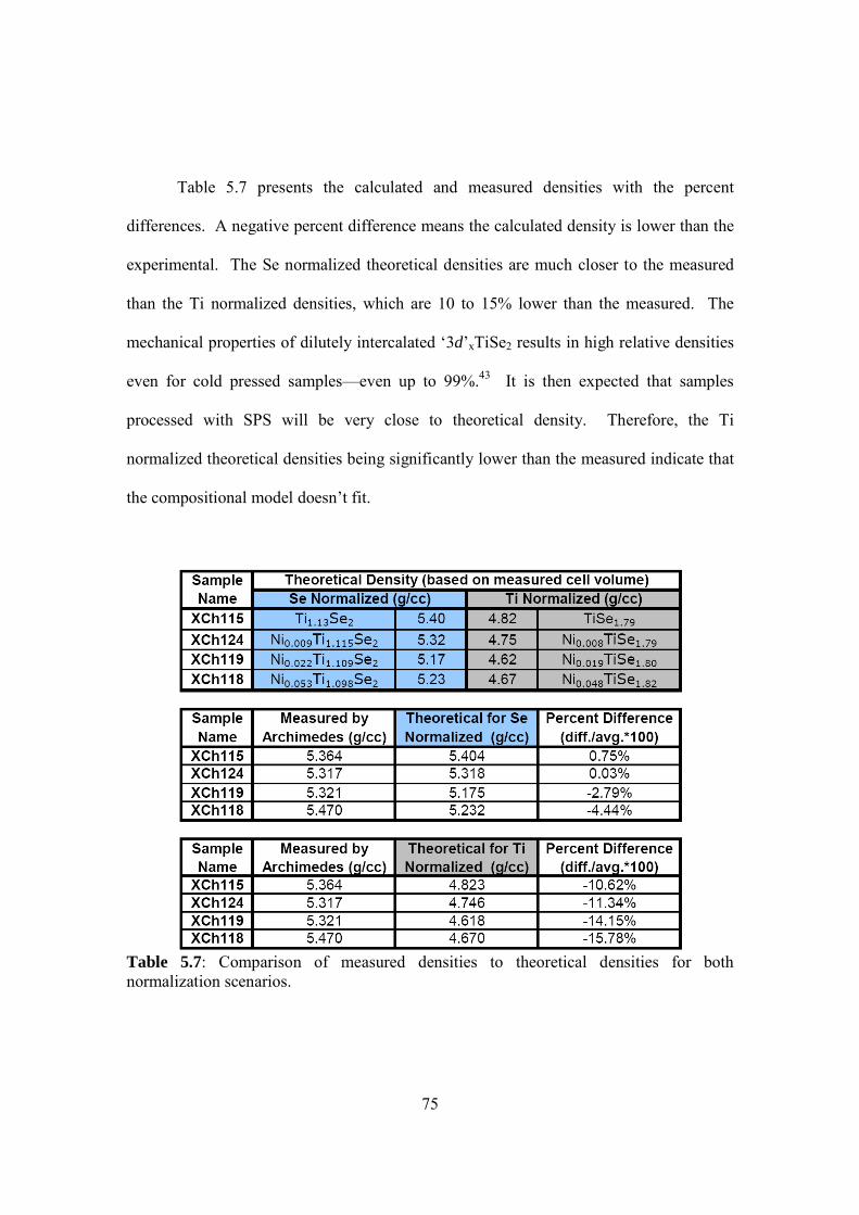
75
Table 5.7 presents the calculated and measured densities with the percent
differences. A negative percent difference means the calculated density is lower than the
experimental. The Se normalized theoretical densities are much closer to the measured
than the Ti normalized densities, which are 10 to 15% lower than the measured. The
mechanical properties of dilutely intercalated ‘3d’xTiSe2 results in high relative densities
even for cold pressed samples—even up to 99%.43 It is then expected that samples
processed with SPS will be very close to theoretical density. Therefore, the Ti
normalized theoretical densities being significantly lower than the measured indicate that
the compositional model doesn’t fit.
Table 5.7: Comparison of measured densities to theoretical densities for both normalization scenarios.

76
While the Se normalized theoretical densities are much closer than those of the Ti
normalized to experimental values, the percent difference is still a little high. This
difference comes partly from the uncertainty involved with the density measurement,
which is on the order of 1 – 2%. An additional source of error is in the determined lattice
parameters. While the XRD data indicates a single phase, the peaks used to determine
the lattice are a bit complex in terms of their width and shape. This is due to the effects
of two different intercalant species being dispersed throughout the van der Waals gap,
with each expected to have different effects on the lattice constant (especially the c
parameter).
An additional attempt was made to determine the theoretical density of the
densified samples by considering the intercalated bulk to be made up of several pure
phases with known structural parameters—TiSe (note: the formula of the whole unit cell
is Ti2Se2) and NixTiSe2. The lattice parameters used for cell volume calculations of TiSe
were taken from the literature.60 The lattice parameters used for NixTiSe2 were calculated
using Vegard’s Rule with data obtained from Arnaud et al.61 The total density was then
estimated to be the atomic masses of the elements of each phase summed according to
stoichiometry, divided by the unit cell volume, and then apportioned by the phase
fractions.
2
., '
(1 )( 2 ) 2 ( )
x
Ni Ti Se Ti Seest
Ni TiSe Vegard s Law TiSe
Xm m m m m
V V
δ δρ + − + += + (5.1)
Table 5.8 reveals the details of this calculation while Table 5.9 displays the
resulting theoretical densities, which agree quite well (at least within the limit of the

77
uncertainty of the density measurements) with experimental data. It must be mentioned
that the measured densities do not vary much from sample to sample (less than 3%
between most and less dense), and the spread of the estimated densities is even less
(~1%). In Table 5.10 the contribution to the total estimated density from each phase is
shown. From the EPMA data, it appears that the amount of excess Ti is roughly
inversely related to the amount of Ni. This trend is followed by the phase contributions
of TiSe and NixTiSe2, and the result is only a weak spread in the estimated densities. The
measured densities follow this trend much more than the theoretical densities obtained
from experimental lattice parameters of the system. As discussed in earlier in this
chapter, the peaks of the XRD patterns appear to be complex and defining a single value
for the peak position from which the lattice parameters were determined may not be
valid. These results suggest that the Ni and Ti intercalants do not randomly mix in the
van der Waals gap, but due to their opposite effects on c, they create separate regions of
Ti and Ni intercalation.
78
Table 5.8: Constituent phase cell parameters, volume, and fraction. Literature values were used for constituent lattice parameters and thus cell volumes. Theoretical densities were determined by summing the constituents’ densities scaled by their phase fractions.

79
Table 5.9: Comparison of the measured densities and the densities calculated from volume fractions of constituent phases.
Table 5.10: The individual contributions of the TiSe and NixTiSe2 phases to the total estimated densities. Excess titanium appears to be inversely proportional to the amount of intercalated nickel, though the trend is loosely correlated. The result is that the phase contributions follow the same trend, and the total estimated density is roughly independent of composition within the series.
Table 5.11: The lattice parameters from which the density of the sulfur substituted samples was calculated were determined from low resolution XRD data. The theoretical densities increase with increasing Ni as expected. The measured densities follow the opposite trend and decrease with increasing Ni.

80
Figure 5.1: Comparison of pre- and post-SPS. While the c lattice parameter calculated by the (001) peak was calculated to have expanded, the shift in the (002) peak indicates the van der Waals gap to have decreased slightly.
XXRRDD AAnnaallyyssiiss Before
SPS
(101)
(002)
NiSe2 Peaks
Broadening due
to disorder
Shift in c

81
Figure 5.2a: The (001) peak of all samples could not be easily profiled using single peaks. This is the best possible fit obtained for XCh115.
Figure 5.2b: The (001) peak of XCh115 is a convolution of two peaks.

82
Figure 5.3: Deconvolution of the (001) peaks of XCh124 and XCh119. The area fraction of a second peak required to fit the peak becomes less as the Ni and excess Ti increase.

83
CHAPTER SIX
THERMAL TRANSPORT PROPERTIES
Low Temperature Specific Heat Capacity of NixTi1+δSe2
Eq. (3.13) gives the electronic and phononic contributions to the specific heat
capacity as a function of temperature. Dividing the heat capacity by the temperature and
collecting constants results in the temperature (and of course molar) specific heat
capacity to be written as a function of a constant, γ, and a T2 term multiplied by β. The
first constant represents the electronic contribution to the specific heat capacity and β
represents the phononic (lattice) contribution. Plotting cpT-1 versus T2 allows for easy
linear fitting, which will yield the constants of interest.
2pcT
Tγ β= + (5.2)
The results of the fitting are presented in Table 6.1. The Debye temperature
remains nearly constant as the Ni is increased up to sample XCH118 (Ni0.053Ti1.098Se2), of
which θD is increased. Eq. (3.11) defines the Debye temperature and shows its
dependence on the velocity of sounds in the material and density of atoms per unit
volume. The trend in density from Table 5.9 appears to correlate to the trend in θD, and a
plot of both measured and theoretical densities versus Debye temperature is shown in Fig.
6.3.

84
Table 6.1: Results of low temperature ( 5T K< ) fitting of the specific heat. The Debye temperature ( Dθ ) and the Fermi energy (EF) were determined from β and γ, respectively, using Eqs. (3.13) and (5.2).
Low Temperature Thermal Conductivity of NixTi1+δSe2
The intercalation of Ni into Ti1+δSe2 appears to lower the low temperature
crystalline peak that is expected in an ordered crystal with only a few defects/impurities
at the temperature where phonon-phonon scattering compensates the decreasing effect of
defect scattering. This indicates, as may be corroborated by Fig. 5.1, that the Ni adds to
the disorder of the system, and the thermal conductivity below 100 K decreases with
increasing Ni. Towards room temperature, however, the electronic contribution to the
total thermal conductivity comes into play and the higher electrical conductivity of the
samples with more Ni results in an increase in total thermal conductivity of the Ni
intercalated samples over the samples that were not intercalated.
Fig. 6.4 shows the low temperature total thermal conductivity of the NixTi1+δSe2
system. Due to the nature of the measurement technique, the radiative loss must be
corrected for at high temperatures. In order to correct for the radiation that increases with
temperature, the electronic contribution was first calculated using the Wiedemann-Franz
relation shown in Eq. (1.34) with a Lorenz number appropriate for degenerate
semiconductors and semimetals—2.1x10⁻⁸ W-Ω/K2. The electronic contribution was

85
then subtracted and the remaining thermal conductivity attributed to the lattice, κph, and
radiation contributions. The κph vs. temperature curve was then analyzed. At higher
temperatures, above the peak temperature, κph should show a 1/T dependence due to
phonon-phonon interactions. The higher temperature data for κph was fit with a three
term formula accounting for (1) a constant term that indicates the minimum value at
which the κph will saturate, (2) the T-1 dependence of κph, and (3) a T3 radiation term:
3( )ph
Bfit A CT
Tκ = + + (5.3)
This model fit the data above 225 K very well and the total and lattice thermal
conductivities were corrected for radiative losses. Fig. 6.5 shows all the contributions to
the uncorrected total thermal conductivity of XCh118. At room temperature, the
correction is only on the order of 10 to 12%. This was essentially the same for all
samples since sample geometries were very similar. Fig. 6.6 compares the corrected
lattice thermal conductivities of NixTi1+δSe2. Now that the electronic contributions have
been subtracted, there is a clear trend of decreasing lattice thermal conductivity with
increasing Ni for all the samples shown. The lattice thermal conductivity is proportional
to the cube of the Debye temperature divided by the square of the Grüneisen parameter,
( 3 2/ph D Gκ θ γ∝ ),15 and it can be seen from Table 6.1 that the Debye temp of XCh115
(Ti1.130Se2) and XCh119 (Ni0.022Ti1.109Se2) are nearly the same. The reduction in thermal
conductivity must be due to an increase in γG, which is proportional to the thermal
expansion coefficient and inversely proportional to the density ( /G T Dγ α ρ∝ ). The
measured and estimated theoretical densities of are nearly the same (Table 5.9). All of

86
this at least suggest that the decrease in lattice thermal conductivity is due to an increase
in the thermal expansion coefficient, Tα . While this was not measured, it certainly is
possible as the increase of Ni and the disorder it adds to the lattice of the system may
increase the anharmonicity of the phonon modes. While this same argument may suggest
that Tα should also be higher for XCh118 (Ni0.053Ti1.098Se2), the reduction in the Debye
temperature indicates a reduction in available phonon modes. The likely case is that both
a reduction of the phonon density of states as well as an increase in the anharmonicity of
the system is the result for further reduction of the lattice thermal conductivity.
Low Temperature Thermal Conductivity of NixTi1+δSe2-ySy
The sulfur substituted system exhibited a lower total thermal conductivity than the
NixTi1+δSe2 system. As compared to CuxTiSe2-ySy data from Hor and Cava,43 the thermal
conductivities of the NixTi1+δSe2-ySy system are still lower, and show more of an
amorphous behavior (Fig. 6.7). The total and lattice thermal conductivities of the sulfur-
substituted samples were also corrected for radiation loss, and the results are shown in
Figs. 6.8 and 6.9, respectively. It is observed from the data that the lattice thermal
conductivity is not monotonically related to the Ni concentration.
Sample XCh114 (Ni0.037Ti0.996Se1.815S0.185) is the only sample of either series to not
have excess Ti. The small deficiency of Ti may be due to Ni substitution on Ti sites
made energetically favorable by the distortions of the lattice from the sulfur substitutions,
or the deficiency may be false—resulting from the uncertainty of the EPMA data. In
either case, it is interesting to compare samples XCh111 (Ti1.041Se1.787S0.213) and XCh114.

87
Both samples have only one atomic species in the van der Waals gap. As a result, the
intercalants may order themselves within the gap to increase the crystallinity. The two
samples with both Ni and Ti in the gap exhibit more of an amorphous behavior.
All samples of the NixTi1+δSe2-ySy series exhibit both lower total and lattice
thermal conductivity values versus those of the NixTi1+δSe2 series. This is mostly most
likely due to the lower densities of the sulfur-substituted samples (between 4.66 and 4.87
g/cm3 versus 5.32 to 5.47 g/cm3 for the system without sulfur). An additional source of
the reduction in the lattice thermal conductivity may come from the added disorder that
the sulfur creates in the structure of the a-b planes, as well as from the effects of mass
fluctuation on phonon scattering. Perhaps a useful future study would be the effect of
sulfur substitution on the phonon dispersion relation and consequential phonon density of
states.

88
Figure 6.1: Specific heat with Dulong-Petit limit of cv in the inset.

89
Figure 6.2: Specific heat of NixTi1+δSe2 below 5 K. The inset is cpT
-1 plotted versus T2 with linear fit lines.

90
Figure 6.3: Measured and estimated theoretical densities versus the Debye temperatures calculated from low temperature cp data.

91
Figure 6.4: Total thermal conductivity of NixTi1+δSe2 after radiation correction. Inset shows the uncorrected data as measured.

92
Figure 6.5: Radiation correction to the thermal conductivity of Ni0.053Ti1.098Se2. The relative magnitudes of the corrections were comparable between samples.

93
Figure 6.6: Lattice thermal conductivity of NixTi1+δSe2 after radiation correction. The unexpected plateau feature between 75 and 150 K in Ni0.022Ti1.109Se2 is probably a result of the charge density wave transition. This feature may also be present in Ti1.130Se2 but may weaker or be hidden in the higher crystalline peak.

94
Figure 6.7: Total thermal conductivity of NixTi1+δSe2-ySy before radiation correction. Thermal conductivity of similar Cu intercalated compounds from Hor and Cava.43

95
Figure 6.8: Radiation corrected total thermal conductivity of NixTi1+δSe2-ySy.

96
Figure 6.9: Radiation corrected lattice thermal conductivity of NixTi1+δSe2-ySy.

97
CHAPTER SEVEN
ELECTRONIC TRANSPORT PROPERTIES
Electrical Resistivity and Seebeck of NixTi1+δSe2
The electronic transport measurements of the NixTi1+δSe2 system are sensitive to
both the sample species and amount of intercalants. The electronic structure of the
semimetal TiSe2 has special implications for the transport properties when it comes to
doping and alloying. With both holes and electron bands meeting at the Fermi energy at
different k-points, just a few percent of intercalants can significantly affect the number
and sign of the carriers as well as the density of states at the Fermi energy. Appendix A
gives electronic density of states diagrams for several relevant compounds to show the
effects of Ni and excess Ti in the van der Waals gap.
From Fig. 7.1 it can be seen that the intercalation suppresses the magnitude of the
charge density wave (CDW) anomaly as observed from the resistivity versus temperature
curves shown for the NixTi1+δSe2 system. The onset temperature of the anomaly is also
systematically shifted towards lower temperatures. This is a further indication of Ni
inducing disorder in the lattice. In the sample with the most Ni, XCh118
(Ni0.053Ti1.098Se2), there is no evidence of a CDW transition that can be observed.
The low and high temperature Seebeck coefficient (thermopower) values are
compared to the low temperature data of TiSe2 (DiSalvo et al.)59 in Fig. 7.2. In sample
XCh115 (Ti1.130Se2), the CDW peak is considerably suppressed but still at roughly the
same temperature that of pristine TiSe2. The magnitude and temperature dependence of

98
the thermopower above 150 K are, however, very different. The thermopower of TiSe2
rapidly goes to zero and changes sign by room temperature. In XCh115, the
thermopower remains below -50 µV/K up to 575 K with a gently sloping region between
200 and 400 K. By comparing the DOS of TiSe2 in Fig. A-1 with that of Ti1.25Se2 in Fig.
A-2, the addition of Ti into the vacancies of the van der Waals gap results in extra Ti-3d
states just above EF. These bands most likely add electron states and along with itinerate
3d electrons to compensate the hole concentration that must increase with temperature in
the TiSe2 host. This picture is corroborated by the effective carrier concentrations
calculated from the Hall resistivity as shown in (Fig. 7.6).
The addition of Ni into the van der Waals gap further suppresses the charge
density wave anomalies at low temperatures but increases the temperature at which the
maximum thermopower is reached. This temperature, having to do with bipolar
conduction, is related to the ratio of holes to electrons. The trends in the temperature
dependencies of the effective carrier concentrations at room temperature correlate to the
high temperature thermopower data—showing a more negative slope as it approaches the
temperature regime above room temperature as the maximum temperature for the
thermopower is shifted upwards.
The power factor was calculated from the electrical resistivity and the
thermopower ( 2 /PF Tα ρ= ). The linear, metallic behavior of the three samples with the
most nickel (XCh119, XCh123, and XCh124) results in a quadratic trend in their power
factors. Due to the curvature of the thermopower in the samples with less nickel, the PF
exhibits a down turn above ~100 K. The high and full temperature range for the power

99
factors are shown in Fig. 7.4. The high temperature turnover in the power factors of all
samples comes from the bipolar conduction induced turnovers in the thermopower.
XCh123 and XCh118, having the highest thermopower maximum temperature, exhibit
the highest power factors at the highest temperatures.
Low Temperature Electrical Resistivity and Seebeck of NixTi1+δSe2-ySy
The low temperature transport properties of NixTi1+δSe2-ySy were measured and are
compared with those of the Cu intercalated CuxTiSe2-ySy.43 The electrical resistivity
versus temperature curves displayed in Fig. 7.7 shows all the nickel intercalated, sulfur
substituted samples to be metallic with the magnitude of the most resistive sample
remaining under 1 mΩ-cm at room temperature. A clear correlation between the
resistivity and the Ni, excess Ti, or Se:S trends independently. The expected trends are
that the resistivity should increase with increasing Ni and excess Ti, whereas they should
decrease with increasing sulfur. Observing the three samples with Ni, the excess Ti and
the sulfur concentrations decrease with increasing Ni. Additionally, the packing densities
of the samples also decrease with increasing Ni. Unfortunately, there are too many
variables in the system to make a clear correlation of these data with either the Ni or Ti
intercalants. However it is clear that these samples are all considerably lower than those
of the Cu intercalated samples in the reference.
As is typical in thermoelectrics research, the gains in electrical conductivity were
offset with losses in the Seebeck coefficients. Fig. 7.8 presents the low temperature
Seebeck coefficent data of NixTi1+δSe2-ySy and selected samples from the reference. The

100
charge density wave anomaly is unobservable in all NixTi1+δSe2-ySy samples with the
exception of XCh112 (Ni0.011Ti1.036Se1.780S0.220). However, in XCh12, the anomaly is very
small—much smaller than that of XCh115 (Ti1.130Se2) and all the Cu intercalated samples
shown. This indicates that the excess Ti (which is about three times less in all sulfur
substituted samples than in the unsubstituted samples) in conjunction with the
substitution of sulfur is enough to suppress the formation of excitons (hole-electron
pairing), or at least prevent exciton-phonon interactions that result in a CDW. Note that
the Seebeck coefficient of TiSe1.8S0.2 of the reference exhibits quite a large CDW
anomaly.
The power factors of the sulfur substituted samples are plotted with reference data
in Fig. 7.9. Due to the absence of a CDW, all sulfur substituted samples of this work
exhibit a T2 dependence, with the exception of XCh112, which happens to be near linear
above 100 K due to the small presence of the CDW anomaly in the Seebeck coefficient.
This results in XCh112 having the highest power factor at room temperature of about 3.3
Wm-1K-1. The temperature dependencies of the Ni intercalated samples suggests that
their power factor values above room temperature will be higher than the best samples
from Hor and Cava’s work.

101
Figure 7.1: Low temperature electrical resistivity of NixTi1+δSe2.

102
Figure 7.2: Low and high temperature Seebeck coefficients of NixTi1+δSe2 with reference data of pristine TiSe2 from DiSalvo et al.59

103
Figure 7.3: Low temperature Seebeck coefficients of NixTi1+δSe2 with reference data of pristine TiSe2 from DiSalvo et al.59

104
Figure 7.4: Low and temperature power factor of NixTi1+δSe2.

105
Figure 7.5: Low and high temperature power factor of NixTi1+δSe2.
106
Figure 7.6: Effective carrier concentration as a function of temperature.

107
Figure 7.7: Low temperature electrical resistivity of NixTi1+δSe2-ySy.

108
Figure 7.8: Low temperature Seebeck coefficients of NixTi1+δSe2-ySy.

109
Figure 7.9: Low temperature power factors of NixTi1+δSe2-ySy.

110
CHAPTER 8
CONCLUSION AND FINAL REMARKS
The goal of this study was to see if a viable, cheap, and relatively environmentally
safe thermoelectric material can be made from a system that is traditionally hasn’t been
sought after for thermoelectric studies. Despite exhibiting a charge density wave
transition—which competes with thermoelectricity for the Fermi surface—TiSe2 was
chosen to be a good candidate. This is due to its structural and electronic versatility in
terms of the large number of atoms—both in variety and quantity—that it may host in
between its layers, and its unique band structure that is in the “ grey area” between a
metal and semiconductor, and also between a majority hole carrier and majority electron
carrier system.
The structural, thermal, and electronic properties of Ni and Ti co-intercalation do
not follow the conventional trends of the single 3d intercalated TiSe2 systems, including
NixTiSe2. The synergetic combination of two intercalants has provided a new way to
improve the thermoelectric properties of this system. The effects of the intercalants have
been explained and understood in terms of their independent and collaborated effects on
the disorder of the crystal structure, independent effects on the density of electronic states
at the Fermi energy, contribution of carriers to the system, and their effects on the
phononic transport of the system.
The additional parameter of sulfur substitution on the selenium sites has also been
studied and compared to similar recent studies of other, single intercalant systems. The

111
co-intercalation of both Ni and Ti into the mixed system Ti(Se,S)2 has resulted in an
enhanced ZT for this system. To date very little complete thermoelectric data has been
published on 3d-intercalated TiSe2, and Hor and Cava’s work, published in 2009,
represent the current state of the thermoelectric studies of this material. Fig. 8.1 displays
the ZT of NixTi1+δSe2-ySy with that of Hor and Cava’s best sample.
While a ZT of ~0.09 has been realized in sample XCh112 at room temperature,
this is well below the ZT~ 1 – 2 range that the state-of-the-art materials possess.
Therefore, titanium and nickel co-intercalated titanium diselenide, even with sulfur
substitution, are not viable thermoelectrics. Still, these materials are rich in interesting
electrical transport phenomena and have proved to be an ideal system for the
investigation and understanding of the effects on intercalation on the electronic structure
and resulting electronic transport properties.

112
Figure 8.1: Low temperature ZT of NixTi1+δSe2-ySy. The maximum ZT in Hor and Cava’s CuxTiSe2-ySy system was found for x=0.02, y=0.3 with ZT~0.07 at 300 K, over which sample XCh112 (Ni0.011Ti1.036Se1.780S0.220) shows nearly a 30% increase.

113
APPENDICES
Appendix A
Band Structure and Density of States Calculations
The electronic band structures of several compounds were calculated using the
Stuttgard TB-LMTO software package. This program employs the linear muffin tin
orbital (LMTO) and the atomic spheres approximation. Calculations were performed
with 16 points along each k-vector. In the case of intercalated supercells, the lattice
parameters used were multiples of c and a parameters determined by Vegard’s rule.

114
Figure A-1: The extra layer of Ti atoms located in the van der Waals gap at (0 0 ½) result in added states at EF. As shown in Fig. A-2, even just 25% excess Ti results in these added states.
115
Figure A-2: Density of States for TiSe2 with 25% Ni and 25% Ti in the van der Waals gap vacancies.

116
Appendix B
Magnetic Susceptibility of NixTi1+δSe2
Thermoelectric phenomena by nature pertain to the lattice and charge degrees of
freedom, and the magnetic properties that originate from the spin degree of freedom are
usually not of interest in thermoelectric materials research. However, the magnetic
susceptibility at low temperatures may provide some useful information about the
structural and electronic states of the system. The susceptibility is defined as the
moment, M, of a material in an external magnetic field of strength, B.
M
Bχ = (5.4)
Conduction electrons are paramagnetic in terms of their response to an external
magnetic field (actually, the susceptibility of conduction electrons contains both a
paramagnetic term and a weaker, negative diamagnetic term that arises from the Lorentz
force and is equal to one-third the contribution from Pauli paramagnetism).62 While their
susceptibility (χ) should follow a T-1 Curie dependence, the fact that only those electrons
within kBT of EF are available to the conduction bands results in their χ being temperature
independent.51 The paramagnetic susceptibility of conduction electrons is therefore:
21 3
2B
p pF F
k T
T E E
µχ χ∝ ⋅ → = (5.5)
The ion cores of the lattice may also exhibit paramagnetic behavior, but with the
total population participating, the T-1 behavior is observed. However, the ion cores may
exhibit the tendency to ferromagnetically (or antiferromagnetically) order themselves by
way of an exchange field, BE, that must be added to the applied field when evaluating the

117
magnetic susceptibility.63 In the temperature regime where there is enough thermal
energy prevent the ions from actually achieving the ferromagnetic ordering, the result is a
paramagnetic susceptibility that follows the Curie-Weiss Law:51
C W
C
Tχ
θ− =−
(5.6)
The parameter θ is related to the strength of the exchange field, and in
ferromagnets, θ is the Curie temperature (TC)—the temperature at which thermal energy
overcomes the exchange field and the material goes from ferromagnetic to paramagnetic.
This value may be negative, which indicates that there nearest neighbor interactions of
the exchange field are of the antiferromagnetic type. The Curie constant (C) is related to
the effective moment of the paramagnetic ions by the gyromagnetic ratio (g) and the spin
angular momentum (S):
2 22 2( 1)
3 3eff BB
B B
pg S SC
k k
µµ+= = (5.7)
There have been a few studies of the effects of 3d metal intercalation on the
magnetic properties of MxTiSe2.40,64,65,66 At low concentrations of magnetic intercalants,
many of these are paramagnetic with a Curie-Weiss ‘tail’ above 5 K. As with many of
the materials in the references, the magnetic susceptibilities of all samples measured in
this study were fit over the entire temperature regime (~7 – 300 K) with a constant term
that contains all diamagnetic and Pauli free-spin contributions and a Curie-Weiss term:
0 0C W
C
Tχ χ χ χ
θ−= + = +−
(5.8)

118
From Eq. (5.7) the effective moment may be deduced. Comparing the effective
moments of the intercalants (Ti and Se ions have no magnetic moments) with the
corresponding value for a free ion will give an indication of the degree to which the
orbitals of the intercalants are hybridized with the Ti-3d and Se-4p orbitals of the host.65
The effective moment ought to also correlate to the change in the c lattice parameter as
the bonding of the intercalants to the layers of the TiSe2 host matrix will effect the
separation between layers.64,65 If the diamagnetic contribution to 0χ can be calculated,
then the Pauli free-spin term may be calculated and EF estimated from Eq. (5.5).
The magnetic moment versus temperature was measured for a selection of
samples from the NixTi1+δSe2 set using a vibrating sample magnetometer (VSM) option
of a Quantum Design PPMS®. Sample pieces weighing between 25 and 50 mg were cut
from the same pellets from which the bar samples for thermal and electrical transport
measurements were cut. The samples were each placed at the center of a quartz paddle
about 3 inches long, and held in place by heat shrink tubing that covered the whole length
of the paddle. Measurements were taken from 7 K to room temperature under a field of 1
– 2 Tesla.
The magnetic moment was measured on the same selection of samples for which
the heat capacity and high resolution XRD were measured. All samples show a Curie-
Weiss behavior indicating the samples to be paramagnetic. The data was fit to extract the
Pauli paramagnetic contribution from the carrier free spins and the effective moments of
the ions. As with the Debye temperature and other properties, the effective moment of
the localized ions increases with increasing Ni content until sample XCh118. This may

119
indicate that the Ni atoms in sample XCh118 are more strongly bonded to the layers,
which would be supported by the metallic behavior of its resistivity and Seebeck.
Table B-1: The magnetic parameters of NixTi1+δSe2 determined by VSM. The diamagnetic contribution was assumed to be a constant and taken from Baranov et al.64,Error! Bookmark not defined. The data of Baranov et al. is listed here for comparison. In their work, the nickel concentration was nominal and the possibility of excess Ti was not investigated.

120
Figure B-1: Curie-Weiss behavior of the localized magnetic moments of the ions in NixTi1+δSe2.

121
Appendix C
Complete Sample List
Though the scope of this work focuses on the effects of Ni and Ti co-intercalation
in TiSe2 and TiSe1.8S0.2, many other samples were synthesized and the low temperature
electronic transport properties measured. The initial samples (XCh100 – XCh110) were
chosen for thermoelectric investigations based of recent literature reports of similar
compounds (XCh101, -103, -107, and -109), which would become the bases for the work
of this dissertation. Some were selected base on preliminary band structure calculations
(XCh104 – 106, -110), while others were selected purely out of curiosity—note that
these were some of the early samples that, while they showed interesting charge density
wave behavior, they were not potential thermoelectrics (XCh100, -102, and -108). The
samples XCh127 – XCh132 were prepared for the purpose of investigating the effect of
synthesis temperature on the amount of excess Ti, which is discussed in Appendix D.
Table C-1: Complete list of samples synthesized grouped by relevant compositions. The sample number ID follows chronological order of synthesis.

122
Table C-2: Nominal compositions, processing conditions, and room temperature transport properties of all samples.

123
REFERENCES 1 G Vineyard, Phys. Today 12 (1959) 42. 2 AF Ioffe, LS Stil'bans, EK Iordanishvili, TS Stavitskaya, and A Gelbtuch,
Semiconductor Thermoelements and Thermoelectric Cooling (Infosearch, London, 1957).
3 HJ Goldsmid and RW Douglas, “The use of semiconductors in thermoelectric refrigeration” Br. J. Appl. Phys. 5 (1954) 386.
4 E Altenkirch, “Elektrothermische kälteerzeugung und reversible elektrische Heizung” Phys. Z. 12 (1911) 920.
5 AF Ioffe, LS Stil’bans, EK Iordanishvili, and TS Stavitskaya, Termoelektricheskoe Okhlazhdenie. (U.S.S.R. Academy of Sciences, Moscow-Leningrad, 1949).
6 GJ Snyder, “Thermoelectric Power Generation: Efficiency and Compatibility”, Chapter 9 of Thermoelectrics Handbook: Macro to Nano, edited by DM Rowe. (CRC Press, Boca Raton, FL, 2006).
7 W Thompson, Collected Papers I (University Press, Cambridge, 1882), 232-291. 8 L Onsager, Phys. Rev. 37 (1931) 405; 38 (1931) 9 HB Callen, “The Application of Onsager’s Reciprocal Relations to Thermoelectric,
Thermomagnetic, and Galvomagnetic Effects” Phys. Rev. 73 (1948) 1349-1358. 10 P Drude, “Zur Elektronentheorie der Metalle“ Ann. d. Phys. 306 (1900) 566-613. 11 JH Yang, Chapter 1.1 of “Thermal Conductivity: Theory, Properties, and
Applications”, edited by Terry M. Tritt (Kluwer Academic/Plenum Publishers, New York, 2004).
12 John Singleton, Band Theory and Electronic Properties of Solids (Oxford University Press, New York, 2001).
13 A Sommerfeld and NH Frank, “The Statistical Theory of Thermoelectric, Galvano- and Thermomagnetic Phenomena in Metals” Rev. Mod. Phys. 3 (1931) 1-42.
14 NF Mott and H Jones, The Theory of the Properties of Metals and Alloys (Dover for Oxford University Press, New York, 1958).
15 Ctirad Uher, Chapter 1.2 of Thermal Conductivity: Theory, Properties, and Applications, edited by Terry M. Tritt. (Kluwer Academic/Plenum Publishers, New York, 2004).
16 H Fröhlich and C Kittel, “Remark on the Paper by Prof. G. Busch” Physica 20 (1954) 1086.
17 FR Gamble, “Ionicity, Atomic Radii, and Structure in the Layered Dichalcogenides of Groups IVb, Vb, and VIb Transition Metals” J. Solid State Chem. 9 (1974) 358-367.
18 LF Mattheiss, “Band Structures of Transition-Metal-Dichalcogenide Layer Compounds” Phys. Rev. B 8 (1973) 3719-3740.
19 HP Hughes and WY Liang, “Vacuum ultraviolet reflectivity spectra of the disulphides and diselenides of titanium, zirconium, and hafnium” J. Phys. C: Solid State Phys. 10 (1977) 1079-1087.
20 HP Hughes, "Structural distortions in TiSe2 and related materials—a possible Jahn Teller effect?” J. Phys. C: Solid State Phys. 10 (1977) L319-L323.

124
21 AD Yoffe, "Physical Properties of Intercalated Solids" Solid State Ionics 9 & 10
(1983) 59-70. 22 NJ Doran, “Electronic structure and band theory of transition metal dichalcogenides”
Physica B+C 99 (1980) 227-237. 23 A Wilson, FJ Di Salvo, and S Mahajan, "Charge-Density Waves in Metallic, Layered,
Transition-Metal Dichalcogenides" Phys. Rev. Lett. 32 (1974) 882-885. 24 RH Friend, D Jérome, WY Liang, JC Mikkelsen, and AD Yoffe, "Semimetallic
character of TiSe2 and semiconductor character of TiS2 under pressure" J. Phys. C: Solid State Phys. 10 (1977) L705-L708.
25 J von Boehm and HM Isomäki, "Relativisitic p-d gaps of 1T TiSe2, TiS2, ZrSe2 and ZrS2" J. Phys. C.: Solid State Phys. 15 (1982) L733-L737.
26 O Anderson, R Manzke, and M Skibowski, “Three-Dimensional and Relativistic Effects in Layered 1T-TiSe2” Phys. Rev. Lett. 55 (1985) 2188-2191.
27 AW Overhauser, "Exchange and Correlation Instabilities of Simple Metals" Phys. Rev. 167 (1968) 691-698.
28 G Li, WZ Hu, D Qian, D Hsieh, MZ Hasan, E Morosan, RJ Cava, and NL Wang, “Semimetal to semimetal charge density wave transition in 1T-TiSe2” Phys. Rev. Lett. 99 (2007) 027404.
29 JM Lopez-Castillo, A Amara, S Jandl, JP Jay-Gerin, C Ayache, and MJ Aubin, "Phonon-drag effect in TiSe2-xSx mixed compounds" Phys. Rev. B 36 (1987) 4249-4253.
30 MB Dines, "Lithium intercalation via n-Butyllithium of the layered transition metal dichalcogenides" Mater. Res. Bull. 10 (1975) 287-291.
31 MS Whittingham and FR Gamble Jr., "The lithium intercalates of the transition metal dichalcogenides" Mater. Res. Bull. 10 (1975) 363-371.
32 BG Silbernagel, "Lithium intercalation complexes of layered transition metal dichalcogenides: An NMR survey of physical properties" Solid State Commun. 17 (1975) 361-365.
33 C Ramírez and W Schattke, "Diffusion and intercalation of alkali atoms in transition metal dichalcogenides" Surf. Sci. 482-485 (2001) 424-429.
34 FR Gamble and TH Geballe, Inclusion Compounds (Plenum Press, New York, 1976). 35 M Ikebe and Y Muto, “Effect of alloying and intercalation on superconductivity of
transition metal dichalcogenides” Synthetic Met. 5 (1983) 229-244. 36 E Morosan, HW Zandbergen, BS Dennis, JWG Bos, Y Onose, T Klimczuk, AP
Ramirez, NP Ong, and RJ Cava, “Superconductivity in CuxTiSe2” Nature Physics 2 (2006) 544-550.
37 AF Kusmartseva, B Sipos, H Berger, L Forró, and E Tutiš, “Pressure Induced Superconductivity in Pristine 1T-TiSe2” Phys. Rev. Lett. 103 (2009) 236401-4.
38 J van Wezel, P Nahai-Williamson, and SS Saxena, "Exciton-phonon interactions and superconductivity bordering charge order in TiSe2" Phys. Rev. B 83 (2011) 024502-10.
125
39 G Wu, HX Yang, L Zhao, XG Luo, T Wu, GY Wang, and XH Chen, "Transport
properties of single-crystalline CuxTiSe2 (0.015≤x≤0.110)" Phys. Rev. B 76 (2007) 024513.
40 AN Titov, AV Kuranov, VG Pleschev, YM Yarmoshenko, MV Yablonskikh, AV Postnikov, S Plogmann, M Neumann, AV Ezhov, and EZ Kurmaev, "Electronic structure of CoxTiSe2 and CrxTiSe2" Phys. Rev. B 63 (2001) 035106.
41 AA Lakhani, S Jandl, C Ayache, and JP Jay-Gerin, "Thermoelectric power of TiSe2-xSx mixed crystals at low temperatures" Phys. Rev. B 28 (1983) 1978-1982.
42 Y Hirota, K Ichiyama, N Hosoi, Y Oikawa, Y Miyahara, VA Kulbachinskii, and H Ozaki, "Thermoelectric properties of mixed layered compounds TiS2-xSex (0≤×≤2)" IEEE Proceedings of the 21st Annual Conference on Thermoelectrics (2002) 159.
43 YS Hor and RJ Cava, “The low temperature thermoelectric properties of CuxTiSe2-ySy” Mat. Res. Bull. 44 (2009) 1375-1378.
44 AL Pope, RT Littleton IV, and TM Tritt, “Apparatus for the rapid measurement of electrical transport properties for both ‘needle-like’ and bulk materials” Rev. Sci. Instrum. 72 (2001) 3129-3131.
45 AL Pope, B Zawilski, and TM Tritt, "Description of removable sample mount apparatus for rapid thermal conductivity measurements" Cryogenics 41 (2001) 725–731.
46 TM Tritt, “Electrical the Thermal Transport Measurement Techniques for Evaluation of the Figure-of-Merit of Bulk Thermoelectric Materials”, Chapter 23 of Thermoelectrics Handbook: Macro to Nano, edited by DM Rowe. (CRC Press, Boca Raton, FL, 2006).
47 Edwin Hall, "On a New Action of the Magnet on Electric Currents" Am. J. Math. 2 (1987) 287–292.
48 HA Lorentz, “The Motion of Electrons in Metallic Bodies I, II, and III” Proc. K. Ned. Akad. Wet. 7 (1904) 438-453, 585-593, and 684-691.
49 S. O. Kasap, Principles of Electronic Materials and Devices (McGraw-Hill, New York, 2000).
50 P Debye, “Zur Theorie der spezifischen Waerme” Ann. Phys. (Leipzig) 39 (1912) 789. 51 C Kittel, Introduction to Solid State Physics, 8th Ed. (John Wiley and Sons, New York,
2005). 52 R Bachmann, F J DiSalvo, et al. “Heat Capacity Measurements on Small Samples at
Low Temperatures” Rev. Sci. Instrum. 43 (1972) 205. 53 A Petit and P Dulong, "Recherches sur quelques points importants de la Théorie de la
Chaleur" Ann. Chim. Phys. 10 (1819) 395-413. English translation: Ann. of Phil. 14 (1819) 189-198.
54 GS Nolas, J Sharp, and HJ Goldsmid, Thermoelectrics: Basic Principles and New Materials Developments (Springer-Verlag, Berlin/Heidelberg, 2001).
55 WJ Parker, RJ Jenkins, CP Butler, and GL Abbott, "Flash Method of Determining Thermal Diffusivity, Heat Capacity, and Thermal Conductivity" J. Appl. Phys. 32 (1961) 1679-1684.

126
56 AV Sergueeva, DM Hulbert, NA Mara, and AK Mukherjee, “Mechanical Properties of
Nanostructured Materials”, Chapter 3 of Nanostructured Materials, edited by G Wilde. (Elsevier, Oxford, 2009).
57 HB Huntington and AR Grone, "Current-Induced Marker Motion in Gold Wires" J. Phys. Chem. Solids 20 (1961) 76-87.
58 KC Woo, FC Brown, WL McMillan, RJ Miller, MJ Schaffman, and MP Sears, "Superlattice formation in titanium diselenide" Phys. Rev. B 14 (1976) 1342-1347.
59 FJ Di Salvo, DE Moncton, JV Waszczak, “Electronic properties and superlattice formation in the semimetal TiSe2” Phys. Rev. B 14 (1976) 4321-4328.
60 F Gronvold and FJ Langmyhr, “X-Ray Study of Titanium Selenides” Acta Chem. Scand. 15 (1961) 1949-1962.
61 Y Arnaud, M Chevreton, A Ahouandjinou, M Danot, and J Rouxel, “Etude Structurale des Composés MxTiSe2, (M = Fe, Co, Ni)” J. Solid State Chem. 18 (1976) 9-15.
62 U Mizutani, Introduction to the Electron Theory of Metals (Cambridge University Press, Cambridge, 2001).
63 P Weiss, “L'hypothèse du champ moléculaire et la propriété ferromagnétique” J. Phys. Theor. Appl. 6 (1907) 661-690.
64 VG Pleschov, NV Baranov, AN Titov, K Inoue, MI Bartashevich, and T Goto “Magnetic properties of Cr-intercalated TiSe2” J. Alloy. Compd. 320 (2001) 13–17.
65 Y Tazuke and T Takeyama, “Magnetic Properties of 3d Transition Element Intercalated Compounds MxTiSe2” J. Phys. Soc. Jpn. 66 (1997) 827-830.
66 AV Postnikov, M Neumann, S Plogmann, YM Yarmoshenko, AN Titov, and AV Kuranov, “Magnetic properties of 3d-doped TiSe2 and TiTe2 intercalate compounds” Comp. Mater. Sci. 17 (2000) 450-454.