Embed Size (px)
Citation preview
HAL Id: tel-00554333https://tel.archives-ouvertes.fr/tel-00554333
Submitted on 10 Jan 2011
HAL is a multi-disciplinary open accessarchive for the deposit and dissemination of sci-entific research documents, whether they are pub-lished or not. The documents may come fromteaching and research institutions in France orabroad, or from public or private research centers.
L’archive ouverte pluridisciplinaire HAL, estdestinée au dépôt et à la diffusion de documentsscientifiques de niveau recherche, publiés ou non,émanant des établissements d’enseignement et derecherche français ou étrangers, des laboratoirespublics ou privés.
Theoretical and Experimental Studies of SemiconductorBased Photonic Devices for All-Optical Signal
Processing at 40 Gbit/s and BeyondMinh Nguyet Ngo
To cite this version:Minh Nguyet Ngo. Theoretical and Experimental Studies of Semiconductor Based Photonic Devicesfor All-Optical Signal Processing at 40 Gbit/s and Beyond. Engineering Sciences [physics]. UniversitéRennes 1, 2010. English. �NNT : 2010REN1E004�. �tel-00554333�
N d’ordre : 2010REN1E004 Annee 2010
These / Universite de Rennes 1sous le sceau de l’Universite Europeenne de Bretagne
pour le grade de
Docteur de l’Universite de Rennes 1Mention : Physique
Ecole Doctorale : Sciences de la Matierepresentee par
Minh Nguyet Ngopreparee a l’unite de recherche Foton CNRS UMR 6082
Equipe Foton-Enssat/FOT et PERSYSTU.F.R. S.D.L.M.
Theoretical andExperimentalStudies ofSemiconductorBased PhotonicDevices forAll-Optical SignalProcessing at40 Gbit/s andBeyond
These soutenue a Lannionle 20/07/2010
devant le jury compose de :
Herve FOLLIOTProfesseur - INSA de Rennes / President
Jean-Louis OUDARDirecteur de Recherche CNRS - LPN / Rapporteur
Daniel DOLFIIngenieur de Recherche, Expert - Thales R&T /Rapporteur
Ernesto CIARAMELLAMaıtre de Conferences - Scuola SuperioreSant’Anna / Examinateur
Romain BRENOTIngenieur de Recherche et de Formation- Alcatel-Lucent Thales III-V Lab / Examinateur
Jean-Claude SIMONProfesseur - Universite de Rennes 1 / Directeur dethese

ii

To Grandma,to Dad,to Mom
to my dear sis.
A ma grand-mere,a mes parentsa ma p’tite-soeur.
Remerciements
Cette these comme beaucoup d’autres ne peut pas etre menee a bien sans la collaborationet le soutien de nombreuses personnes.
Avant tout, je voudrais exprimer toute ma gratitude a Jean-Claude Simon, directeur dulaboratoire FOTON, pour m’avoir accueilli dans son laboratoire et surtout pour sa directionde cette these. Jean-Claude a su etre efficace malgre les lourdes taches qui l’incombaient.
Je tiens evidemment a remercier les membres du jury, Jean-Louis Oudar, Daniel Dolfi,pour avoir accepter d’etre rapporteurs, Herve Folliot, Romain Brenot et Ernesto Ciaramellapour avoir d’accepter de participer a l’evaluation de mes travaux lors de la soutenance.
On n’oublie pas ses premiers pas. Je souhaite remercier particulierement GwenaelleVaudel et Vincent Roncin pour m’avoir fait decouvrir le monde de la recherche en m’accompagnantpendant toutes premieres manips et tous premiers articles.
Les travaux de cette these ne sont certainement pas menes jusqu’aux resultats au-jourd’hui sans le travail quotidien de l’equipe du platforme Persyst. Je voudrais remercierLaurent Bramerie et Mathilde Gay pour tous leurs conseils et tout le temps qu’ils m’ontaccordee, Sebastien Lobo pour avoir ete toujours disponible dans le laboratoire, Marcia DeCosta Silva et Kevin Lengle pour m’avoir accompagnee avec leur bonne humeur.
Merci a Arthur O’Hare, avec qui j’ai travaille pendant tout un ete a la fin de la these. Unmoment ’stressant’ a devenu finalement un bon souvenir. Son air apaisant, son humour, seshistoires m’ont donne la force pour rester optimiste et motivee. Un ami a qui j’ai partagedes moments inoubliables.
Je n’oublie pas des gens qui ont donne beaucoup de temps pour me transferer leurscompetences et leurs precieuses experiences. Merci a Monique Thual pour m’avoir apprisa faire des fibres microlentillees (que j’en fait pleines plus tard), merci a Philippe Rochardpour m’avoir appris a faire des modules de laser (que je puisse en fait toute seule maintenantcomme une grande). Et merci a Stephane Balac qui m’a fait tellement progresse sur mescompetences en modelisation.
Je tiens aussi a remercier toutes les personnes du laboratoire FOTON avec lesquellesj’ai pu travaille ou simplement passe un bon cafe ensemble : Pascal Bernard, ThierryChartier, Patrice Feron, Jean-Marc Goujon, Olivier Vaudel, Stephane Blin, Jean-FrancoisHayau, Alexandra Lagrost, Sylvain Feve, Ronan Le Page. J’ai une pensee particuliere auxpersonnels administratifs et techniques : Danielle Graviou, Rejane Le Roy, Nelly Vaucelle,Catherine Delen, Michelle Grout, Serge Le Flecher, Henry L’her, Michel Guillou, StephaneChehayed, Christian Sauquet, sans qui je n’aurai pas eu un esprit aussi libre pour plongerdans mon travail dans le laboratoire.
Je voudrais egalement remercier Liam Barry, Douglas Reid, Jesper Mork, Mike VanDer Poel, Per Lunnemann Hansen, Sara Ek pour m’avoir accueilli pendant plusieurs se-maines dans leurs laboratoires a Dublin et a Copenhague. Avec peu de temps mais si bonenvironnement, j’ai pu profite des echanges d’idees tres fructueux.
J’adresse une grande gratitude a Irene et Michel Joindot, qui ont accepte de relire lemanuscrit, sans qui le rapport de these n’aura certainement pas la qualite d’aujourd’hui.
Merci a mes amis : Ngoc, Romain, Shan, et mes amis vietnamiens a Lannion pour leuramitie et leur humour.
Merci a ma famille pour leur inconditionnel amour et leur confiance (comme toujours).Merci a Trung qui etait toujours la, a mes cotes et qui a devenu ma famille.
Contents
List of Acronyms viii
List of Figures viii
List of Tables viii
Introduction 1
I Semiconductor Optical Amplifiers for 2R Regeneration 7
1 Optical fibre communication systems and all-optical regeneration 9
1.1 Optical fibre communication systems . . . . . . . . . . . . . . . . . . . . . . 9
1.1.1 Transmission link description . . . . . . . . . . . . . . . . . . . . . . 10
1.1.2 Modulation formats . . . . . . . . . . . . . . . . . . . . . . . . . . . 11
1.1.2.1 NRZ format . . . . . . . . . . . . . . . . . . . . . . . . . . 11
1.1.2.2 RZ format . . . . . . . . . . . . . . . . . . . . . . . . . . . 12
1.1.3 Transmitter . . . . . . . . . . . . . . . . . . . . . . . . . . . . . . . . 12
1.1.4 Receiver . . . . . . . . . . . . . . . . . . . . . . . . . . . . . . . . . . 14
1.1.5 Signal degradations . . . . . . . . . . . . . . . . . . . . . . . . . . . 15
1.1.5.1 Fibre losses . . . . . . . . . . . . . . . . . . . . . . . . . . . 15
1.1.5.2 Chromatic dispersion . . . . . . . . . . . . . . . . . . . . . 17
1.1.5.3 Polarisation Mode Dispersion . . . . . . . . . . . . . . . . . 19
1.1.5.4 Non-linear effects . . . . . . . . . . . . . . . . . . . . . . . 20
1.1.5.5 Amplified spontaneous emission . . . . . . . . . . . . . . . 21
1.1.6 Transmission quality criteria . . . . . . . . . . . . . . . . . . . . . . 22
1.1.6.1 Optical Signal to Noise Ratio . . . . . . . . . . . . . . . . . 22
1.1.6.2 Eye diagrams . . . . . . . . . . . . . . . . . . . . . . . . . . 23
1.1.6.3 Quality factors . . . . . . . . . . . . . . . . . . . . . . . . . 24
1.1.6.4 Bit Error Rate . . . . . . . . . . . . . . . . . . . . . . . . . 25
1.2 Signal regeneration and all-optical techniques . . . . . . . . . . . . . . . . . 29
1.2.1 Signal regeneration . . . . . . . . . . . . . . . . . . . . . . . . . . . . 29
1.2.1.1 1R regeneration . . . . . . . . . . . . . . . . . . . . . . . . 30
1.2.1.2 2R regeneration . . . . . . . . . . . . . . . . . . . . . . . . 30
1.2.1.3 3R regeneration . . . . . . . . . . . . . . . . . . . . . . . . 32
1.2.2 Techniques for all-optical 2R regeneration . . . . . . . . . . . . . . . 33
vi CONTENTS
1.2.2.1 Fibre based devices . . . . . . . . . . . . . . . . . . . . . . 33
1.2.2.2 Semiconductor Optical Amplifier based devices . . . . . . . 35
1.2.2.3 Microcavity Saturable Absorber based devices . . . . . . . 36
1.3 Chapter summary . . . . . . . . . . . . . . . . . . . . . . . . . . . . . . . . 38
2 Experimental characterisation of different SOA structures 39
2.1 Semiconductor Optical Amplifiers for optical signal processing . . . . . . . . 39
2.1.1 SOA basic description . . . . . . . . . . . . . . . . . . . . . . . . . . 41
2.1.2 Gain saturation . . . . . . . . . . . . . . . . . . . . . . . . . . . . . . 45
2.1.3 SOA dynamics . . . . . . . . . . . . . . . . . . . . . . . . . . . . . . 49
2.1.3.1 Gain dynamics . . . . . . . . . . . . . . . . . . . . . . . . . 49
2.1.3.2 Phase dynamics . . . . . . . . . . . . . . . . . . . . . . . . 51
2.2 Static characteristics . . . . . . . . . . . . . . . . . . . . . . . . . . . . . . . 54
2.2.1 Description of the investigated SOAs . . . . . . . . . . . . . . . . . . 54
2.2.2 Amplified spontaneous emission investigation . . . . . . . . . . . . . 56
2.2.3 Static gain measurements . . . . . . . . . . . . . . . . . . . . . . . . 60
2.3 Dynamics characterisation . . . . . . . . . . . . . . . . . . . . . . . . . . . . 65
2.3.1 Gain dynamics experiment . . . . . . . . . . . . . . . . . . . . . . . 66
2.3.2 Gain compression-response time trade-off . . . . . . . . . . . . . . . 68
2.3.3 Impact of bias current . . . . . . . . . . . . . . . . . . . . . . . . . . 71
2.3.4 Recovery acceleration by shifted filtering in wavelength conversion . 74
2.3.4.1 Physical mechanisms . . . . . . . . . . . . . . . . . . . . . 74
2.3.4.2 Experimental results . . . . . . . . . . . . . . . . . . . . . . 78
2.3.5 Impact of the SOA length . . . . . . . . . . . . . . . . . . . . . . . . 81
2.3.6 Impact of probe wavelength . . . . . . . . . . . . . . . . . . . . . . . 83
2.3.7 Impact of pulse duration . . . . . . . . . . . . . . . . . . . . . . . . . 86
2.3.8 Limit of gain recovery acceleration by assist light . . . . . . . . . . . 88
2.3.9 SOA dynamics assessment by degenerate pump-probe experiment . . 90
2.3.10 Phase dynamics . . . . . . . . . . . . . . . . . . . . . . . . . . . . . 93
2.4 Chapter summary . . . . . . . . . . . . . . . . . . . . . . . . . . . . . . . . 95
3 Numerical study of SOA dynamics 97
3.1 SOA model . . . . . . . . . . . . . . . . . . . . . . . . . . . . . . . . . . . . 97
3.2 Gain and phase dynamics of SOA . . . . . . . . . . . . . . . . . . . . . . . . 101
3.2.1 Fitting process for relaxation time evaluation . . . . . . . . . . . . . 101
3.2.2 Gain dynamics investigation . . . . . . . . . . . . . . . . . . . . . . . 102
3.2.2.1 Gain compression-response time trade-off . . . . . . . . . . 102
3.2.2.2 Influence of probe signal power on gain dynamics . . . . . 104
3.2.2.3 Limit of gain recovery acceleration by assist light . . . . . . 104
3.2.3 Phase dynamics investigation . . . . . . . . . . . . . . . . . . . . . . 106
3.2.3.1 Rate equation of phase evolution . . . . . . . . . . . . . . . 106
3.2.3.2 Contributions of intraband and interband processes to phasechanges . . . . . . . . . . . . . . . . . . . . . . . . . . . . . 107
3.2.3.3 Phase recovery time for various gain compressions . . . . . 107
3.2.3.4 Gain and phase delay . . . . . . . . . . . . . . . . . . . . . 108
3.3 Chapter summary . . . . . . . . . . . . . . . . . . . . . . . . . . . . . . . . 110
CONTENTS vii
4 Investigation of SOA optical gates for 2R regeneration at 40 Gbit/s 111
4.1 Semiconductor optical amplifier for noise compression . . . . . . . . . . . . 112
4.1.1 Principle . . . . . . . . . . . . . . . . . . . . . . . . . . . . . . . . . 112
4.1.2 Noise compression assessment of SOA in self-saturation . . . . . . . 113
4.2 Experimental assessment of 2R regenerator schemes based on cascades ofSOA and SA . . . . . . . . . . . . . . . . . . . . . . . . . . . . . . . . . . . 116
4.2.1 Principles . . . . . . . . . . . . . . . . . . . . . . . . . . . . . . . . . 116
4.2.1.1 Saturable absorber for optical regeneration . . . . . . . . . 116
4.2.1.2 Cascade of SOA and SA for 2R regeneration . . . . . . . . 117
4.2.2 First configuration: SOA followed by SA . . . . . . . . . . . . . . . . 118
4.2.2.1 Eye diagrams observations . . . . . . . . . . . . . . . . . . 120
4.2.2.2 Results of BER measurements . . . . . . . . . . . . . . . . 121
4.2.3 Second configuration: SA followed by SOA . . . . . . . . . . . . . . 122
4.2.3.1 Eye diagrams observations . . . . . . . . . . . . . . . . . . 123
4.2.3.2 Results of BER measurements . . . . . . . . . . . . . . . . 124
4.2.4 Spectrum deformation . . . . . . . . . . . . . . . . . . . . . . . . . . 125
4.3 Numerical study of the SOA-SA regenerator . . . . . . . . . . . . . . . . . . 127
4.3.1 Modelling descriptions . . . . . . . . . . . . . . . . . . . . . . . . . . 127
4.3.2 Impact of the SOA response time . . . . . . . . . . . . . . . . . . . . 130
4.3.3 Impact of the SA reflectivity . . . . . . . . . . . . . . . . . . . . . . 132
4.4 Chapter summary . . . . . . . . . . . . . . . . . . . . . . . . . . . . . . . . 133
II All-Optical Clock Recovery 135
Introduction on all-optical clock recovery 137
5 All-optical clock recovery for 3R regeneration 139
5.1 Clock recovery . . . . . . . . . . . . . . . . . . . . . . . . . . . . . . . . . . 139
5.1.1 Role of clock recovery function in optical networks . . . . . . . . . . 139
5.1.2 Different techniques for clock extraction . . . . . . . . . . . . . . . . 140
5.1.2.1 Filtering technique . . . . . . . . . . . . . . . . . . . . . . . 140
5.1.2.2 Phase-locked loop technique . . . . . . . . . . . . . . . . . 142
5.1.2.3 Injection locking in oscillating systems without retroaction 143
5.2 Solution based on self-pulsating semiconductor lasers . . . . . . . . . . . . . 144
5.2.1 Operation principle . . . . . . . . . . . . . . . . . . . . . . . . . . . . 145
5.2.2 Advantages and limitations . . . . . . . . . . . . . . . . . . . . . . . 145
6 Experimental study of all-optical clock recovery devices based on self-pulsating semiconductor lasers 149
6.1 Characterisation techniques . . . . . . . . . . . . . . . . . . . . . . . . . . . 149
6.1.1 Components characteristics . . . . . . . . . . . . . . . . . . . . . . . 149
6.1.2 Timing jitter . . . . . . . . . . . . . . . . . . . . . . . . . . . . . . . 150
6.1.3 Temporal analysis . . . . . . . . . . . . . . . . . . . . . . . . . . . . 151
6.1.4 Spectral analysis . . . . . . . . . . . . . . . . . . . . . . . . . . . . . 151
6.1.5 Remodulation technique . . . . . . . . . . . . . . . . . . . . . . . . . 153
6.1.6 System analysis . . . . . . . . . . . . . . . . . . . . . . . . . . . . . . 154
6.2 Clock recovery performances of bulk based and quantum-dot based SP lasers 154
6.2.1 Experimental set-up . . . . . . . . . . . . . . . . . . . . . . . . . . . 154
viii CONTENTS
6.2.2 Results of BER measurements . . . . . . . . . . . . . . . . . . . . . 1556.3 Passive pre-filtering for performance enhancement . . . . . . . . . . . . . . 157
6.3.1 Proposed configuration using passive pre-filtering . . . . . . . . . . . 1576.3.2 Filter characterisation . . . . . . . . . . . . . . . . . . . . . . . . . . 1586.3.3 Temporal and spectral analyses . . . . . . . . . . . . . . . . . . . . . 1616.3.4 Results of BER measurements . . . . . . . . . . . . . . . . . . . . . 162
6.4 Polarisation sensitivity assessment . . . . . . . . . . . . . . . . . . . . . . . 1646.4.1 Experimental set-up . . . . . . . . . . . . . . . . . . . . . . . . . . . 1646.4.2 Polarisation sensitivity of QD-SP laser based OCR . . . . . . . . . . 1656.4.3 Polarisation sensitivity of SP laser cascade based OCR . . . . . . . . 166
6.5 Resistance to polarisation mode dispersion . . . . . . . . . . . . . . . . . . . 1676.5.1 PMD emulator . . . . . . . . . . . . . . . . . . . . . . . . . . . . . . 1686.5.2 Impact of PMD on receiver sensitivity . . . . . . . . . . . . . . . . . 1686.5.3 Resistance of bulk-SP laser based OCR to PMD effect . . . . . . . . 171
Summary of optical clock recovery investigations 174
Conclusions 178
Bibliography 183
Appendix 1: Jahn’s SOA model 199
Appendix 2: Agrawal’s SOA model 206
Appendix 3: Publications 210

List of Acronyms
1R Reamplifying
2R Reshaping Reamplifying
3R Retiming Reshaping Reamplifying
AR Anti-Reflection
ASE Amplified Spontaneous Emission
ASK Amplitude Shift Keying
BER Bit Error Rate
BG-FP filter Bragg Grating Fabry-Perot filter
BH Buried Heterostructure
BP Band-Pass
CB Conduction Band
CH Carrier Heating
CR Clock Recovery
CW Continuous Wave
DBR Distributed Bragg Reflector
DCF Dispersion Compensating Fibre
DFB Distributed FeedBack
DGD Differential Group Delay
DH Double Heterojunctions
DI Delay Interferometer
DPSK Differential Phase Shift Keying
DSF Dispersion Shifted Fibre
EA ElectroAbsorption
EAM ElectroAbsorption Modulator
EDFA Erbium Doped Fibre Amplifier
ER Extinction Ratio
ETDM Electrical Time Division Multiplexing
FEC Forward Error Correction Code
FSK Frequency Shift Keying
FSR Free Spectral Range
FWM Four Wave Mixing
FTTH Fiber To The Home
GVD Group Velocity Dispersion
HNL Highly Non-Linear
IC Integrated Circuit
ISI InterSymbole Interference

x CONTENTS
LAN Local Area Network
MAN Metro Area Network
MFD Mode Field Diameter
NF Noise Figure
NOLM Non-linear Optical Loop Mirror
NRZ Non Return to Zero
NZ-DSF Non Zero Dispersion Shifted Fibre
OC Optical Circulator
OCR Optical Clock Recovery
OSA Optical Spectrum Analyser
OSNR Optical Signal to Noise Ratio
OSO Optical Sampling Oscilloscope
OTDM Optical Time Division Multiplexing
PC Polarisation Controller
PLL Phase Locked Loop
PMD Polarisation Mode Dispersion
PON Passive Optical Network
PRBS Pseudo Random Bit Sequence
PSD Power Spectral Density
PSK Phase Shift Keying
QD Quantum-Dot
QW Quantum-Well
QWR Quantum-Wire
RF Radio Frequency
RMS Root-Mean Square
R-SOA Reflective Semiconductor Optical Amplifier
RZ Return to Zero
SA Saturable Absorber
SBS Stimulated Brillouin Scattering
SHB Spectral Hole Burning
SMF Single Mode Fibre
SOA Semiconductor Optical Amplifier
SOA-MZI SOA-based Mach-Zehnder Interferometer
SP Self-Pulsating
SPM Self Phase Modulation
SRS Stimulated Raman Scattering
SSB Single Side Band
TDM Time Division Multiplexing
TE Transverse Electric
TM Transverse Magnetic
TPA Two Photon Absorption
VB Valence Band
VCO Voltage Controlled Oscillator
VOA Variable Optical Attenuator
WAN Wide Area Network
WDM Wavelength Division Multiplexing
WL Wetting Layer
XGM Cross Gain Modulation
XPM Cross Phase Modulation
List of Figures
1.1 Point-to-point fibre links with periodic loss compensation through (a) regen-erators and (b) optical amplifiers . . . . . . . . . . . . . . . . . . . . . . . . 10
1.2 Example of an NRZ format signal in time (a) and in spectral domains (b) . 11
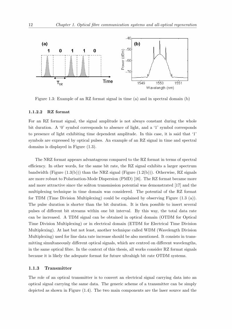
1.3 Example of an RZ format signal in time (a) and in spectral domain (b) . . 12
1.4 Generic scheme of an optical transmitter . . . . . . . . . . . . . . . . . . . . 13
1.5 Generic scheme of a digital optical receiver . . . . . . . . . . . . . . . . . . 14
1.6 Illustration of an RZ format signal at a transmitter output (a) and the signalafter a long fibre transmission (b) . . . . . . . . . . . . . . . . . . . . . . . . 15
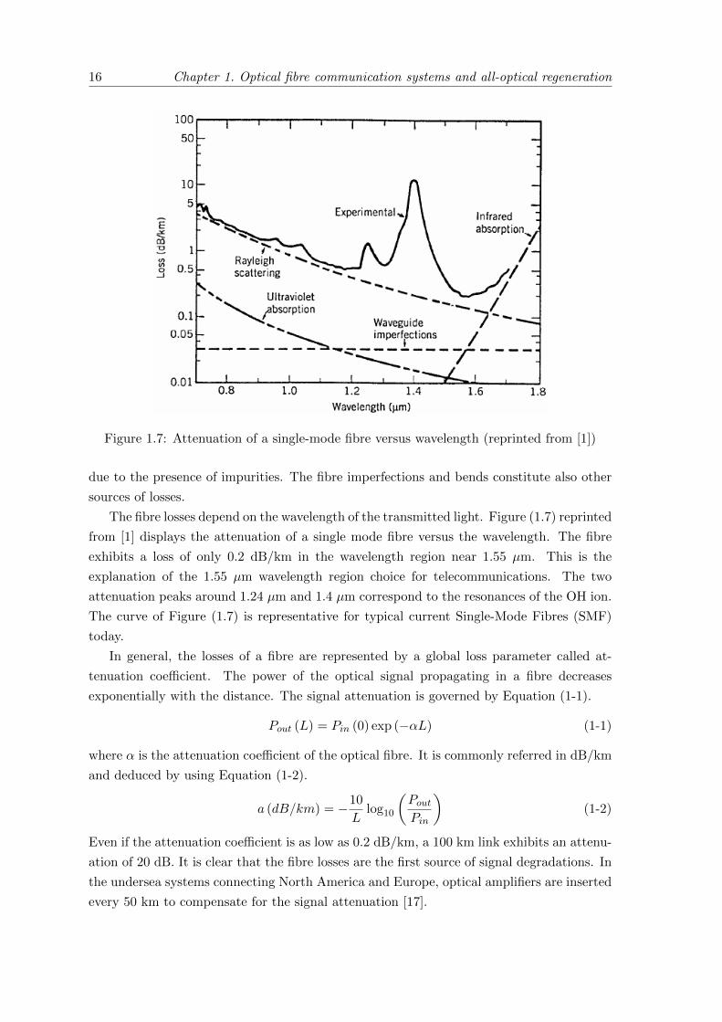
1.7 Attenuation of a single-mode fibre versus wavelength (reprinted from [1]) . 16
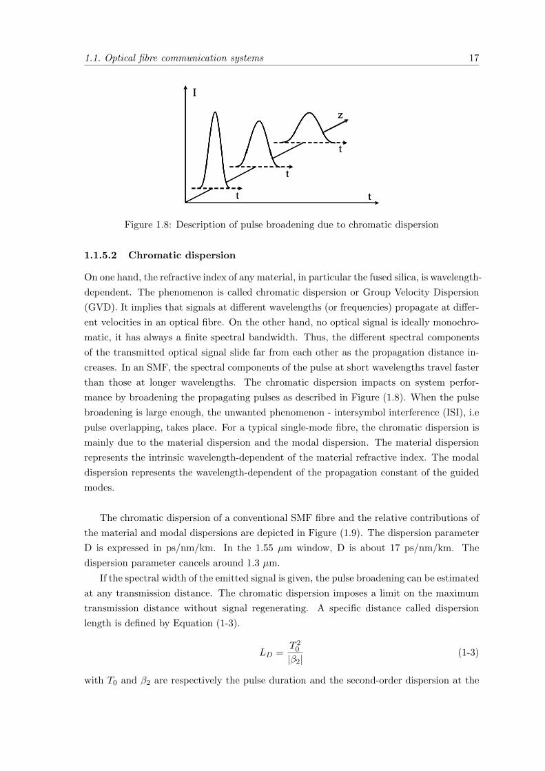
1.8 Description of pulse broadening due to chromatic dispersion . . . . . . . . . 17
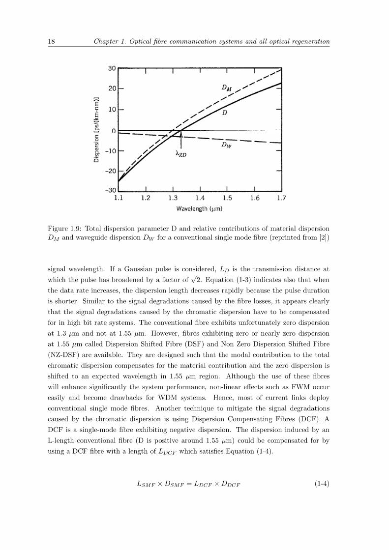
1.9 Total dispersion parameter D and relative contributions of material disper-sion DM and waveguide dispersion DW for a conventional single mode fibre(reprinted from [2]) . . . . . . . . . . . . . . . . . . . . . . . . . . . . . . . . 18
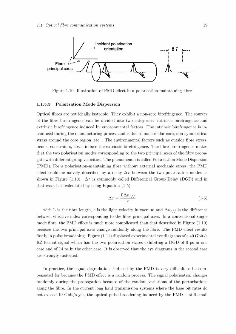
1.10 Illustration of PMD effect in a polarisation-maintaining fibre . . . . . . . . 19
1.11 Experimental eye diagrams of a 40 Gbit/s RZ format signal exhibiting 0 psDGD (a) and 14 ps DGD (b) . . . . . . . . . . . . . . . . . . . . . . . . . . 20
1.12 Illustration of FWM in a 10 km Dispersion Shifted Fibre . . . . . . . . . . . 22
1.13 Principle of OSNR measurement using OSA . . . . . . . . . . . . . . . . . . 23
1.14 Electrical (a) and optical (b) eye diagrams of an RZ signal . . . . . . . . . . 24
1.15 Illustration of amplitude fluctuation on electrical eye diagrams and detectedvoltage histogram . . . . . . . . . . . . . . . . . . . . . . . . . . . . . . . . . 25
1.16 Illustration of timing jitter on electrical eye diagrams and correspondinghistogram . . . . . . . . . . . . . . . . . . . . . . . . . . . . . . . . . . . . . 26
1.17 Examples of BER vs input receiver power curves . . . . . . . . . . . . . . . 27
1.18 Illustration of three regeneration levels: reamplifying, reshaping and retimingof an RZ format signal . . . . . . . . . . . . . . . . . . . . . . . . . . . . . . 29
1.19 Principle of 1R regeneration . . . . . . . . . . . . . . . . . . . . . . . . . . . 30
1.20 Reshaping principle with step-like characteristic function . . . . . . . . . . . 31
1.21 Generic scheme of 2R regenerator in self-modulation regime . . . . . . . . . 31
1.22 Generic scheme of 2R regenerator in cross-modulation regime . . . . . . . . 32
1.23 Generic scheme of 3R regeneration . . . . . . . . . . . . . . . . . . . . . . . 33
1.24 Generic scheme of fibre based NOLM . . . . . . . . . . . . . . . . . . . . . . 34
1.25 Schematic diagram of Mamyshev regenerator (reprinted from [3]) . . . . . . 34
1.26 Principle scheme of an SOA Mach-Zehnder Interferometer in differential con-figuration . . . . . . . . . . . . . . . . . . . . . . . . . . . . . . . . . . . . . 36
2.1 Picture of an SOA (a) and cross-section scheme of a buried heterostructure (b) 41
xii LIST OF FIGURES
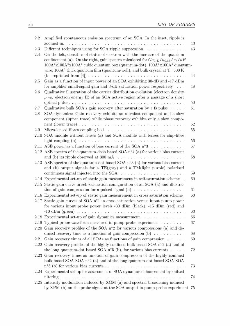
2.2 Amplified spontaneous emission spectrum of an SOA. In the inset, ripple iszoomed in. . . . . . . . . . . . . . . . . . . . . . . . . . . . . . . . . . . . . . 43
2.3 Different techniques using for SOA ripple suppression . . . . . . . . . . . . 43
2.4 On the left, densities of states of electron with the increase of the quantumconfinement (a). On the right, gain spectra calculated forGa0.47In0.53As/InP100A◦x100A◦x100A◦ cubic quantum box (quantum-dot), 100A◦x100A◦ quantum-wire, 100A◦ thick quantum film (quantum-well), and bulk crystal at T=300 K(b - reprinted from [4]) . . . . . . . . . . . . . . . . . . . . . . . . . . . . . . 44
2.5 Gain as a function of input power of an SOA exhibiting 30-dB and -17 dBmfor amplifier small-signal gain and 3-dB saturation power respectively . . . 48
2.6 Qualitative illustration of the carrier distribution evolution (electron densityρ vs. electron energy E) of an SOA active region after a passage of a shortoptical pulse . . . . . . . . . . . . . . . . . . . . . . . . . . . . . . . . . . . . 50
2.7 Qualitative bulk SOA’s gain recovery after saturation by a fs pulse . . . . . 51
2.8 SOA dynamics: Gain recovery exhibits an ultrafast component and a slowcomponent (upper trace) while phase recovery exhibits only a slow compo-nent (lower trace) . . . . . . . . . . . . . . . . . . . . . . . . . . . . . . . . . 52
2.9 Micro-lensed fibres coupling bed . . . . . . . . . . . . . . . . . . . . . . . . 55
2.10 SOA module without lenses (a) and SOA module with lenses for chip-fibrelight coupling (b) . . . . . . . . . . . . . . . . . . . . . . . . . . . . . . . . . 56
2.11 ASE power as a function of bias current of the SOA n◦3 . . . . . . . . . . . 57
2.12 ASE spectra of the quantum-dash based SOA n◦4 (a) for various bias currentand (b) its ripple observed at 300 mA . . . . . . . . . . . . . . . . . . . . . 58
2.13 ASE spectra of the quantum-dot based SOA n◦3 (a) for various bias currentand (b) output signals for a TE(gray) and a TM(light purple) polarisedcontinuous signal injected into the SOA . . . . . . . . . . . . . . . . . . . . 59
2.14 Experimental set-up of static gain measurement in self-saturation scheme . 60
2.15 Static gain curve in self-saturation configuration of an SOA (a) and illustra-tion of gain compression for a pulsed signal (b) . . . . . . . . . . . . . . . . 61
2.16 Experimental set-up of static gain measurement in cross saturation scheme 63
2.17 Static gain curves of SOA n◦1 in cross saturation versus input pump powerfor various input probe power levels -30 dBm (black), -15 dBm (red) and-10 dBm (green) . . . . . . . . . . . . . . . . . . . . . . . . . . . . . . . . . 63
2.18 Experimental set-up of gain dynamics measurement . . . . . . . . . . . . . 66
2.19 Typical probe waveform measured in pump-probe experiment . . . . . . . . 67
2.20 Gain recovery profiles of the SOA n◦2 for various compressions (a) and de-duced recovery time as a function of gain compression (b) . . . . . . . . . . 68
2.21 Gain recovery times of all SOAs as functions of gain compression . . . . . . 69
2.22 Gain recovery profiles of the highly confined bulk based SOA n◦2 (a) and ofthe long quantum-dot based SOA n◦5 (b), for various bias currents . . . . . 72
2.23 Gain recovery times as function of gain compression of the highly confinedbulk based SOA-SOA n◦2 (a) and of the long quantum-dot based SOA-SOAn◦5 (b) for various bias currents . . . . . . . . . . . . . . . . . . . . . . . . . 73
2.24 Experimental set-up for assessment of SOA dynamics enhancement by shiftedfiltering . . . . . . . . . . . . . . . . . . . . . . . . . . . . . . . . . . . . . . 74
2.25 Intensity modulation induced by XGM (a) and spectral broadening inducedby XPM (b) on the probe signal at the SOA output in pump-probe experiment 75
LIST OF FIGURES xiii
2.26 Simulated impact of filter position with respect to the initial probe signalwavelength on recovery profile . . . . . . . . . . . . . . . . . . . . . . . . . . 75
2.27 Probe transmittance (dashed line) at the blue-shifted filter output and evo-lutions of the SOA gain (red line) and of the induced chirp (blue line) . . . 76
2.28 Numerical results of SOA+filter system dynamics for a fixed output modula-tion ratio of 3 dB for different position of filter. (a-c) SOA gain modulationin three cases and(d-f) corresponding output probe signal . . . . . . . . . . 77
2.29 Experimental probe spectra at the SOA output and in front of the filter(black curves) and the filter shapes with a blue-shift (blue curve) in (a) andwith a red-shift (red curve) in (c). Probe spectra at the filter output in caseof blue-shifted filtering (b) and of red-shifted filtering (d) . . . . . . . . . . 79
2.30 Experimental probe waveforms at the (QDot SOA + filter) output for differ-ent configurations: (a) centred filter, (b) red-shifted filter and (c) blue-shiftedfilter . . . . . . . . . . . . . . . . . . . . . . . . . . . . . . . . . . . . . . . . 80
2.31 Measured gain recovery waveforms at maximum bias current of the 2-mmQDot SOA (a) and of the 5-mm QDot SOA (b) for various gain compressions 81
2.32 Measured gain recovery waveforms at low input probe power level for the2-mm length QDot SOA and the 5-mm length QDot SOA . . . . . . . . . . 82
2.33 ASE spectrum of the 2-mm QDot SOA at 200 mA of bias current and re-spective positions of pump and probe signals in both experiments . . . . . . 84
2.34 Gain recovery forms of the 2-mm QDot SOA(SOA n◦3) for two differentprobe wavelengths (a) and time axis is expanded in (b) . . . . . . . . . . . 84
2.35 Static gain measurements (a) and recovery time evolutions as functions ofgain compression (b) at different wavelengths . . . . . . . . . . . . . . . . . 86
2.36 Gain recovery waveforms for various gain compressions and for pump pulsedurations of 2.5 ps (a) and of 7.5 ps (b) (SOA n◦6) . . . . . . . . . . . . . . 87
2.37 Recovery time as functions of gain compression for different pump pulsedurations . . . . . . . . . . . . . . . . . . . . . . . . . . . . . . . . . . . . . 88
2.38 Gain recovery waveforms for various ratios Pprobe/Psat and for pump pulsedurations of 2.5 ps (a) and of 7.5 ps (b) (SOA n◦6). Gain compression wasfixed at 3 dB. . . . . . . . . . . . . . . . . . . . . . . . . . . . . . . . . . . . 89
2.39 Experimental and triple-exponential fit of gain recovery trace of the SOAn◦3. In inset, the curve is expanded. . . . . . . . . . . . . . . . . . . . . . . 91
2.40 Experimental gain recovery trace of the SOA n◦3 from the picosecond exper-iment and a bi-exponential fit (a), or a triple-exponential fit (b) . . . . . . . 92
2.41 Experimental phase recovery of the 2-mm length QDot SOA for different biascurrents (measurements of Per Lunnemann and Sara Ek of DTU Fotonik) . 93
3.1 Static gain (a) and dynamic gain (b) curves of the SOA n◦2. The staticgain curve was obtained in auto saturation configuration without the probesignal. The dynamic gain curve was obtained with Pprobe/Psat = 10 dB andthe gain compression was 3 dB. . . . . . . . . . . . . . . . . . . . . . . . . . 102
3.2 Gain recovery shapes of the SOA n◦2 for gain compressions of 1.7 dB (a) and5 dB (b) with Pprobe/Psat = 10dB . . . . . . . . . . . . . . . . . . . . . . . . 103
3.3 Gain recovery shapes for various gain compressions (a) and deduced recoverytimes (b) with Pprobe/Psat = 10dB . . . . . . . . . . . . . . . . . . . . . . . 103
xiv LIST OF FIGURES
3.4 Gain recovery shapes for various ratios Pprobe/Psat (a) and evolutions ofcorresponding recovery time and gain compression (b) with Ppump/Psat =−2.5 dB . . . . . . . . . . . . . . . . . . . . . . . . . . . . . . . . . . . . . . 104
3.5 Gain recovery shapes for various ratios Pprobe/Psat at a fixed gain compressionof 3 dB with (a) current density of 1 (a.u) and (b) current density of 1.5 (a.u)105
3.6 Phase recovery for various values of αT . The gain compression was fixed at3 dB and α = 5. In inset, the curves are expanded. . . . . . . . . . . . . . . 107
3.7 Phase recovery shapes (a) and deduced recovery times (b) for various gaincompressions with Pprobe/Psat = 10 dB . . . . . . . . . . . . . . . . . . . . . 108
3.8 Observation of gain compression and phase deviation delay, αT = 1 and α = 5109
3.9 Synchronisation of phase and gain modulations in case αT = α = 5 . . . . . 110
4.1 Gain as a function of input power of an SOA (a) and characteristic functionof an optical gate based on the SOA in self-saturation (b) . . . . . . . . . . 112
4.2 Set-up for noise compression experiment using SOA in self-saturation . . . . 113
4.3 Signal eye diagrams at the SOA optical gate input (a) and at the SOA opticalgate output for input signal powers of -5 dBm (b), of -2 dBm (c) and thecorresponding gain compression traces (d), (e) respectively . . . . . . . . . . 114
4.4 BER evolution vs decision threshold (a) and vs Rx input power (b) of thedata signals at the SOA optical gate input and output for different gaincompressions . . . . . . . . . . . . . . . . . . . . . . . . . . . . . . . . . . . 115
4.5 Photograph of SA chip, fibre array and SA module . . . . . . . . . . . . . . 116
4.6 SA reflectivity as a function of input power . . . . . . . . . . . . . . . . . . 117
4.7 Reflectivity of an SA (a), gain of an SOA (b) and transmission function of acascade SOA-SA (c) . . . . . . . . . . . . . . . . . . . . . . . . . . . . . . . 118
4.8 Experimental set-up for noise compression assessment of the first regeneratorconfiguration (SOA followed by SA) . . . . . . . . . . . . . . . . . . . . . . 119
4.9 Eye diagrams of the cross-gain modulated signal at the SOA output . . . . 120
4.10 Signal eye diagrams at the regenerator input (a), after passing through theSOA (b) and at the regenerator output (SA output) (c) . . . . . . . . . . . 120
4.11 BER evolution vs decision threshold (a) and vs Rx input power (b) of datasignals at the regenerator input, output and at the SOA output . . . . . . . 121
4.12 Experimental set-up for noise compression assessment of the second regener-ator configuration (SA followed by SOA) . . . . . . . . . . . . . . . . . . . . 122
4.13 Signal eye diagrams at the regenerator input (a), after passing through theSA (b) and at the regenerator output (Filter 1 output) (c) . . . . . . . . . . 123
4.14 BER evolution vs decision threshold (a) and vs Rx input power (b) of datasignals at the regenerator input, output and at the SA output . . . . . . . . 124
4.15 Spectrum evolutions of the optical signal passing through the regenerator inthe two configurations . . . . . . . . . . . . . . . . . . . . . . . . . . . . . . 126
4.16 Reflectivity spectrum of the SA . . . . . . . . . . . . . . . . . . . . . . . . . 127
4.17 Experiment scheme of the numerical study . . . . . . . . . . . . . . . . . . . 127
4.18 Modelled and measured SA reflectivity evolutions versus input power . . . . 128
4.19 Signal eye diagrams at the regenerator input (a) and output (b) and thecorresponding BER evolutions versus decision threshold (c), with an OSNRof 15 dB/nm for the transmitted signal . . . . . . . . . . . . . . . . . . . . . 129
4.20 SA reflectivity (a) and SOA gain (b) recoveries . . . . . . . . . . . . . . . . 130
LIST OF FIGURES xv
4.21 Evolutions of 40 Gbit/s signal Q factor (black squares) and of extinctionratio (red circles) for various long life-time of the SOA . . . . . . . . . . . . 131
4.22 Noise reduction on the ‘space’ level of the output signal when the SOA longlife-time decreases from 80 ps (a) to 20 ps (b) . . . . . . . . . . . . . . . . . 132
4.23 Evolution of 40 Gbit/s signal Q factor versus SA small-signal reflectivity . . 1324.24 BER evolutions of the regenerator output signal for different SA reflectivities:
-14 dB (black squares) and -25 dB (red circles) . . . . . . . . . . . . . . . . 133
5.1 Operating principle of an optical CR based on spectral line filtering technique1415.2 Basic structure of a conventinal phase-locked loop for CR . . . . . . . . . . 1425.3 Operation of an OCR using SP laser in unlocked regime (a) and locked regime
(b) . . . . . . . . . . . . . . . . . . . . . . . . . . . . . . . . . . . . . . . . . 146
6.1 Eye diagrams of an injected data signal (yellow) and the extracted clock(green) delivered by an SP laser . . . . . . . . . . . . . . . . . . . . . . . . . 151
6.2 Example phase noise curve shapes of an injected data signal (red) and clockdelivered by a CR(black) . . . . . . . . . . . . . . . . . . . . . . . . . . . . . 152
6.3 Principle of the remodulation experiment . . . . . . . . . . . . . . . . . . . 1536.4 Experimental set-up for BER measurements of two CR configurations based
on bulk-SP and QD-SP lasers . . . . . . . . . . . . . . . . . . . . . . . . . . 1556.5 BER of a function of Rx input power for 2 OCRs based on bulk-SP laser and
QD-SP laser . . . . . . . . . . . . . . . . . . . . . . . . . . . . . . . . . . . . 1566.6 Scheme of OCR configuration consisting of a Bragg Gratings Fabry-Perot
filter followed by the bulk-SP laser . . . . . . . . . . . . . . . . . . . . . . . 1576.7 Transmission spectrum of the BG-FP filter . . . . . . . . . . . . . . . . . . 1596.8 Temporal trace (upper) and spectral trace (lower) of the intermediate optical
clock delivered by the BG-FP filter . . . . . . . . . . . . . . . . . . . . . . . 1606.9 Output recovered clock pulses recovered by the bulk-SP laser when an optical
data signal is injected (a) and an optical clock is injected (b) . . . . . . . . 1616.10 Clock phase noise curves obtained when the bulk-SP laser is injected optical
data (bright curve) and an optical clock (dark curve) . . . . . . . . . . . . . 1626.11 BER as a function of Rx input power for two OCR schemes: the bulk-SP
laser alone (green) and with the BG-FP filter for pre-filtering (red) . . . . . 1636.12 Experimental set-up for polarisation sensitivity assessment . . . . . . . . . . 1646.13 BER as a function of Rx input power measured on the remodulated clock
recovered by the QD-SP laser based OCR for various input signal polarisationorientations . . . . . . . . . . . . . . . . . . . . . . . . . . . . . . . . . . . . 165
6.14 Induced penalty at a BER of 10−9 as a function of input signal polarisationangle . . . . . . . . . . . . . . . . . . . . . . . . . . . . . . . . . . . . . . . . 166
6.15 OCR configuration based on cascade of the two SP lasers . . . . . . . . . . 1666.16 BER as a function of Rx input power of remodulated clock provided by the
OCR constituted of cascade of the two SP lasers for various input signalpolarisation orientations . . . . . . . . . . . . . . . . . . . . . . . . . . . . . 167
6.17 Experimental set-up for assessment of PMD impact on receiver sensitivity . 1686.18 Scheme of receiver opto-electronic CR . . . . . . . . . . . . . . . . . . . . . 1696.19 Signal eye diagrams (yellow) and clock temporal traces recovered by receiver
optoelectronic CR circuit(green) for various DGD values of injected data signal1696.20 BER as a function of Rx input power in back-to-back configuration for various
DGD values of optical data signal . . . . . . . . . . . . . . . . . . . . . . . . 170

xvi LIST OF FIGURES
6.21 Experimental set-up for PMD resistance assessment of an OCR based onbulk-SP laser . . . . . . . . . . . . . . . . . . . . . . . . . . . . . . . . . . . 171
6.22 Signal eye diagrams in front of the bulk-SP laser OCR (yellow) and extractedclock signals (green) for various DGD values . . . . . . . . . . . . . . . . . . 172
6.23 BER as a function of Rx input power of remodulated clock given by bulk-SPlaser OCR for various DGD of the transmitted data signal . . . . . . . . . . 173
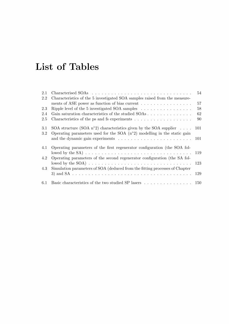
List of Tables
2.1 Characterised SOAs . . . . . . . . . . . . . . . . . . . . . . . . . . . . . . . 542.2 Characteristics of the 5 investigated SOA samples raised from the measure-
ments of ASE power as function of bias current . . . . . . . . . . . . . . . . 572.3 Ripple level of the 5 investigated SOA samples . . . . . . . . . . . . . . . . 582.4 Gain saturation characteristics of the studied SOAs . . . . . . . . . . . . . . 622.5 Characteristics of the ps and fs experiments . . . . . . . . . . . . . . . . . . 90
3.1 SOA structure (SOA n◦2) characteristics given by the SOA supplier . . . . 1013.2 Operating parameters used for the SOA (n◦2) modelling in the static gain
and the dynamic gain experiments . . . . . . . . . . . . . . . . . . . . . . . 101
4.1 Operating parameters of the first regenerator configuration (the SOA fol-lowed by the SA) . . . . . . . . . . . . . . . . . . . . . . . . . . . . . . . . . 119
4.2 Operating parameters of the second regenerator configuration (the SA fol-lowed by the SOA) . . . . . . . . . . . . . . . . . . . . . . . . . . . . . . . . 123
4.3 Simulation parameters of SOA (deduced from the fitting processes of Chapter3) and SA . . . . . . . . . . . . . . . . . . . . . . . . . . . . . . . . . . . . . 129
6.1 Basic characteristics of the two studied SP lasers . . . . . . . . . . . . . . . 150

xviii LIST OF TABLES

Introduction

Introduction 3
Today, information is transmitted throughout the world mainly through digital com-
munication systems with a bit rate, expressed in number of transmitted bits per second,
depending on the applications. Data flow from your USB key to your computer at typi-
cal speed of 480 Mbit/s. Internet providers announce 100 Mbit/s subscriber connections
thanks to recent FTTH (Fibre-To-The-Home) deployments [5]. The optical fibres of the
SEA-ME-WE 3 cables [6], which connect 33 countries and 4 continents from Western Eu-
rope (including France) to the Far East (including Vietnam) and Australia, offer a total
capacity of 480 Gbit/s (48 wavelengths carrying 10 Gbit/s). Regardless of the position in
the networks, the bandwidth demand grows continuously, mainly due to the growth of data
traffic. The transmission capacity of the optical fibre links can be expanded by increasing
both the number of WDM (Wavelength Division Multiplexing) channels and the bit rate
per WDM channel. The base rate of the backbone networks is likely moving from 10 Gbit/s
to 40 Gbit/s [7]. The capacity limit of the present networks is set largely by the use of
electronic elements. For the generation 160 Gbit/s TDM systems, while electronic signal
processing is not available yet, many fundamental functions based on optical devices are
attracting a lot of investigations [8].
In long and ultralong haul links such as submarine intercontinental connections, the
transmitted optical signal has to be amplified periodically. For the bit rates exceeding
40 Gbit/s, deployment of only opto-electronic repeaters will increase dramatically the sys-
tem complexity, cost and power consumption. Long term solutions for signal regeneration
in future high capacity optical networks concern all-optical regeneration which could allow
optical data transmission over virtually unlimited distances. All-optical regenerators used
for future WDM networks must satisfy at least the conditions of low power consumption,
compactness, low-cost and WDM compatibility. Since many years, all-optical regenerators
and their sub-functions have been extensively studied at FOTON laboratory, where this
thesis has been realised. Some important works should be mentioned. A polarisation in-
sensitive 3R regenerator based on semiconductor based NOLM architecture which allows
a cascade of at least 1000 repeaters without any detected error has been demonstrated at
10 Gbit/s [9]. At this bit rate, a high performance WDM compatible 2R regenerator based
on a Saturable Absorber (SA) and a Semiconductor Optical Amplifier (SOA) allowing the
transmission over 11000 km with only 18 cascaded regenerators for a BER of 10−4 [10]. 2R
and 3R regenerators for 40 Gbit/s operation have been also successfully developed. The 2R
regenerator, which is a combination of an SA and a fibre followed by an optical filter, allows
a distance improvement ratio of at least 3.3 among its 8 channels [11]. The regenerator
is WDM compatible and potentially low-cost. 3R regeneration using synchronous modula-
tion allows significant margin enhancements on receiver decision time and threshold to be
obtained [12]. The transmission distance has been also improved from 13000 km to 90000
km in comparison with 2R regeneration case (without the synchronous modulation). Such
3R regeneration quality could not be obtained without the Optical Clock Recovery (OCR)
consisting of a cascade of a bulk based Self-Pulsating (bulk-SP) laser and a Quantum-Dot
4 Introduction
Self-Pulsating (QD-SP) laser. The good timing jitter filtering of the OCR is attributed to
the QD-SP laser, which was demonstrated multi-data-rate compatible [13] and therefore
totally adequate for applications in high bit rate OTDM systems.
The key elements of the all-optical regenerators are non-linear optical gate and OCR
device. The objectives of this thesis were to develop and explore different non-linear gates
and OCRs based on semiconductor technology for optical signal regeneration at 40 Gbit/s
and beyond. As sub-functions for 2R regeneration, non-linear gates based on Semiconductor
Optical Amplifier (SOA) were considered. The high non-linearity of the SOA is its greatest
advantage for optical signal processing. Besides its cost efficiency, compactness, potential
integrability, wide spectral bandwidth and low power consumption are other features which
explain why the SOA continues to receive a lot of attention. As far as OCR devices are
concerned, different configurations using SP lasers were assessed in system environment. A
simple solution was also proposed to enhance the recovered clock quality.
The content of the thesis is divided into two parts with 4 and 2 chapters respectively.
The first part including 4 chapters is dedicated to the results of the investigations on
SOA based non-linear optical gates for 2R regeneration.
Chapter 1 outlines basic notions about optical fibre communication systems which are
used in the manuscript. The reviewed definitions are point-to-point transmission link, usual
modulation formats (RZ and NRZ), transmitter and receiver. Signal degradations during
propagation inside optical fibres are described to highlight the need for signal regeneration
and typical criteria used to specify signal quality are defined. To limit signal impairments
and increase the transmission distance, in-line repeaters are inserted periodically into the
fibre link. The repeaters could provide different regeneration capacities. The principles
of 1R (Reamplifying), 2R (Reamplifying and Reshaping) and 3R (Reamplifying, Reshap-
ing and Retiming) regenerations are described. Finally, a brief review on SOA based 2R
regenerators is presented.
Chapter 2 is devoted to a basic description of Semiconductor Optical Amplifiers and
especially their non-linear properties and high speed dynamics which are used for signal
regeneration. Under saturation by short pulses (of a few picoseconds), it is found that
ultrafast dynamics due to intraband relaxation effects could be exploited for high speed sig-
nal processing. Results of experimental study of different SOA structures are summarised.
These SOAs have been designed and manufactured by the Alcatel-Lucent Thales III-V Lab
in the framework of the French national project FUTUR for all-optical regeneration applica-
tions. The experimental investigations are focused on two main aspects: gain non-linearity
and gain dynamics. The results suggest that highly confined bulk based SOAs and long
quantum-dot SOAs are good candidates for operations at bit rates exceeding 40 Gbit/s. Nu-
merical investigations demonstrate that by associating the long quantum-dot liked sample
with assist techniques such as shifted filtering, operation at 160 Gbit/s without patterning
Introduction 5
effects could be possible.
Chapter 3 is dedicated to numerical study of the SOA dynamics. According to the
experimental results presented in Chapter 2, numerical investigations are necessary to ex-
amine the influences of ultrafast processes on the gain dynamics and consequently on the
reshaping capability of the SOA based 2R regenerator schemes. A simple phenomelogical
SOA model including intraband effects will be useful to realise these preliminary studies.
Such an SOA model, based on that proposed by [14] and then developed by [15], allows
deeper understanding of SOA gain and phase dynamics to be obtained.
Chapter 4 investigates signal reshaping capability of cascades of an SOA and a saturable
absorber. Amplitude noise compression experiments demonstrate the signal regeneration
capability of the SOA-SA regenerators. The complementary roles of the SOA and SA in the
reshaping task are clarified by analysing noise transformation effects when the two devices
operate separately. Finally, a numerical study using the SOA model developed in Chapter
3 explains how the regenerator performance changes when the device intrinsic parameters
change.
The second part including 2 chapters is devoted to the study on SP laser based OCR
devices for 3R regeneration.
Chapter 5 reviews the different roles of the clock recovery (CR) function in transmission
systems. Usual clock extraction techniques and their advantages as well as their limitations
are discussed. Especially, the principle and the state-of-the-art of the CR technique using
SP semiconductor lasers are detailed.
Chapter 6 presents all experimental assessments realised on different OCR configura-
tions. The optical clock signal extracted by the OCR based on a bulk-SP laser exhibits
insufficient quality to be used for regeneration applications. The introduction of a pas-
sive pre-filtering in front of the laser is explored to enhance the recovered clock quality.
Otherwise, a quantum-dot SP laser allows high quality clock to be obtained but such OCR
function is strongly polarisation sensitive. Therefore, polarisation sensitivity of the different
OCRs is assessed. At last, a primary study is devoted to OCR resistance to Polarisation
Mode Dispersion.

6 Introduction
Part I
Semiconductor Optical Amplifiers
for 2R Regeneration

Chapter 1
Optical fibre communication
systems and all-optical
regeneration
In this chapter, basic notions on optical fibre communication systems are reviewed. The
basics of all-optical regeneration as well as the devoted techniques are also developed. The
purpose of the chapter is to describe the thesis context and to present the essential notions
in the manuscript.
In the first section, a basic transmission link concept of optical fibre communication sys-
tems is depicted. The largely used modulation formats (NRZ and RZ) are then described.
Fundamental elements of the transmission link including transmitter and receiver are dis-
cussed. Next, we focus on the main signal degradations induced during the transmission
over fibre links. At last, typical criteria used to specify signal quality are defined.
In the second section, all-optical regeneration processes (1R, 2R and 3R) and associated
techniques are firstly developed. Secondly, reshaping devices using SOA which are studied
during this thesis are discussed. Their different operating configurations are described and
a review of literature is also presented.
1.1 Optical fibre communication systems
The optical fibre communication systems can be found in any level of the network: core
network, Wide Area Network (WAN), Metro Area Network (MAN), Local Area Network
(LAN) and access network. Long haul fibre links (thousands of kilometres) such as subma-
rine cables constitute the backbone or the core of a telecommunication network. A WAN
is usually constituted of communication links covering a broad area such as a country. A
MAN is optimized for a geographical area ranging from several blocks of buildings to entire
cities. A LAN is a network covering a smaller area such as a campus or a building. On one
hand, access network are likely in the same order as a LAN. On the other hand, the ‘access
10 Chapter 1. Optical fibre communication systems and all-optical regeneration
FibreTx TxRx
FibreTxRx Rx
FibreTxRx
Transmitter Regenerator Regenerator Regenerator Receiver
FibreTx
FibreRx
Fibre
Transmitter Receiver
Optical amplifier
Optical amplifier
Optical amplifier
(a)
(b)
FibreTx TxRx
FibreTxRx Rx
FibreTxRx
Transmitter Regenerator Regenerator Regenerator Receiver
FibreTx TxRx TxRx
FibreTxRx TxRx Rx
FibreTxRx Rx
FibreTxRx TxRx
Transmitter Regenerator Regenerator Regenerator Receiver
FibreTx
FibreRx
Fibre
Transmitter Receiver
Optical amplifier
Optical amplifier
Optical amplifier
FibreTx
FibreRx
Fibre
Transmitter Receiver
Optical amplifier
Optical amplifier
Optical amplifier
(a)
(b)
Figure 1.1: Point-to-point fibre links with periodic loss compensation through (a) regener-ators and (b) optical amplifiers
network’ term refers to the last transmission links which connect final users (subscribers)
to their immediate service (telephone, television, Internet) provider. As an example of fibre
links in access network, Fibre-To-The-Home (FTTH) service has been available in France
from March 2007. All these networks can be designed by using point-to-point, point-to-
multipoint, hub, ring or star topology. However, the most practical topology varies from
one to another.
1.1.1 Transmission link description
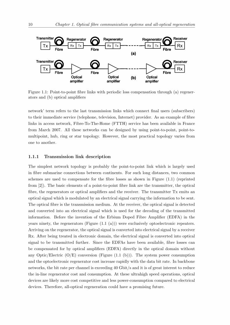
The simplest network topology is probably the point-to-point link which is largely used
in fibre submarine connections between continents. For such long distances, two common
schemes are used to compensate for the fibre losses as shown in Figure (1.1) (reprinted
from [2]). The basic elements of a point-to-point fibre link are the transmitter, the optical
fibre, the regenerators or optical amplifiers and the receiver. The transmitter Tx emits an
optical signal which is modulated by an electrical signal carrying the information to be sent.
The optical fibre is the transmission medium. At the receiver, the optical signal is detected
and converted into an electrical signal which is used for the decoding of the transmitted
information. Before the invention of the Erbium Doped Fibre Amplifier (EDFA) in the
years ninety, the regenerators (Figure (1.1 (a))) were exclusively optoelectronic repeaters.
Arriving on the regenerator, the optical signal is converted into electrical signal by a receiver
Rx. After being treated in electronic domain, the electrical signal is converted into optical
signal to be transmitted further. Since the EDFAs have been available, fibre losses can
be compensated for by optical amplifiers (EDFA) directly in the optical domain without
any Optic/Electric (O/E) conversion (Figure (1.1 (b))). The system power consumption
and the optoelectronic regenerator cost increase rapidly with the data bit rate. In backbone
networks, the bit rate per channel is exceeding 40 Gbit/s and it is of great interest to reduce
the in-line regenerator cost and consumption. At these ultrahigh speed operations, optical
devices are likely more cost competitive and less power-consumption compared to electrical
devices. Therefore, all-optical regeneration could have a promising future.
1.1. Optical fibre communication systems 11
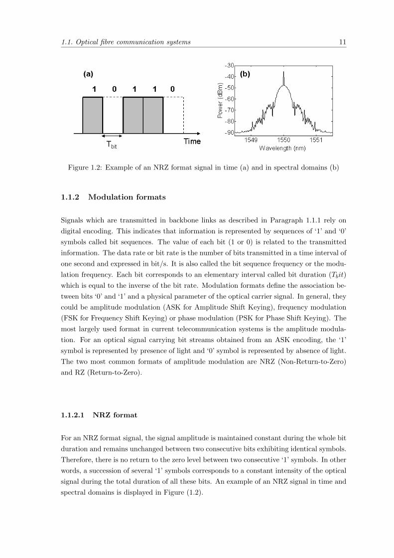
Figure 1.2: Example of an NRZ format signal in time (a) and in spectral domains (b)
1.1.2 Modulation formats
Signals which are transmitted in backbone links as described in Paragraph 1.1.1 rely on
digital encoding. This indicates that information is represented by sequences of ‘1’ and ‘0’
symbols called bit sequences. The value of each bit (1 or 0) is related to the transmitted
information. The data rate or bit rate is the number of bits transmitted in a time interval of
one second and expressed in bit/s. It is also called the bit sequence frequency or the modu-
lation frequency. Each bit corresponds to an elementary interval called bit duration (Tbit)
which is equal to the inverse of the bit rate. Modulation formats define the association be-
tween bits ‘0’ and ‘1’ and a physical parameter of the optical carrier signal. In general, they
could be amplitude modulation (ASK for Amplitude Shift Keying), frequency modulation
(FSK for Frequency Shift Keying) or phase modulation (PSK for Phase Shift Keying). The
most largely used format in current telecommunication systems is the amplitude modula-
tion. For an optical signal carrying bit streams obtained from an ASK encoding, the ‘1’
symbol is represented by presence of light and ‘0’ symbol is represented by absence of light.
The two most common formats of amplitude modulation are NRZ (Non-Return-to-Zero)
and RZ (Return-to-Zero).
1.1.2.1 NRZ format
For an NRZ format signal, the signal amplitude is maintained constant during the whole bit
duration and remains unchanged between two consecutive bits exhibiting identical symbols.
Therefore, there is no return to the zero level between two consecutive ‘1’ symbols. In other
words, a succession of several ‘1’ symbols corresponds to a constant intensity of the optical
signal during the total duration of all these bits. An example of an NRZ signal in time and
spectral domains is displayed in Figure (1.2).
12 Chapter 1. Optical fibre communication systems and all-optical regeneration
Figure 1.3: Example of an RZ format signal in time (a) and in spectral domain (b)
1.1.2.2 RZ format
For an RZ format signal, the signal amplitude is not always constant during the whole
bit duration. A ‘0’ symbol corresponds to absence of light, and a ‘1’ symbol corresponds
to presence of light exhibiting time dependent amplitude. In this case, it is said that ‘1’
symbols are expressed by optical pulses. An example of an RZ signal in time and spectral
domains is displayed in Figure (1.3).
The NRZ format appears advantageous compared to the RZ format in terms of spectral
efficiency. In other words, for the same bit rate, the RZ signal exhibits a larger spectrum
bandwidth (Figure (1.3(b))) than the NRZ signal (Figure (1.2(b))). Otherwise, RZ signals
are more robust to Polarisation-Mode Dispersion (PMD) [16]. The RZ format became more
and more attractive since the soliton transmission potential was demonstrated [17] and the
multiplexing technique in time domain was considered. The potential of the RZ format
for TDM (Time Division Multiplexing) could be explained by observing Figure (1.3 (a)).
The pulse duration is shorter than the bit duration. It is then possible to insert several
pulses of different bit streams within one bit interval. By this way, the total data rate
can be increased. A TDM signal can be obtained in optical domain (OTDM for Optical
Time Division Multiplexing) or in electrical domain (ETDM for Electrical Time Division
Multiplexing). At last but not least, another technique called WDM (Wavelength Division
Multiplexing) used for line data rate increase should be also mentioned. It consists in trans-
mitting simultaneously different optical signals, which are centred on different wavelengths,
in the same optical fibre. In the context of this thesis, all works consider RZ format signals
because it is likely the adequate format for future ultrahigh bit rate OTDM systems.
1.1.3 Transmitter
The role of an optical transmitter is to convert an electrical signal carrying data into an
optical signal carrying the same data. The generic scheme of a transmitter can be simply
depicted as shown in Figure (1.4). The two main components are the laser source and the
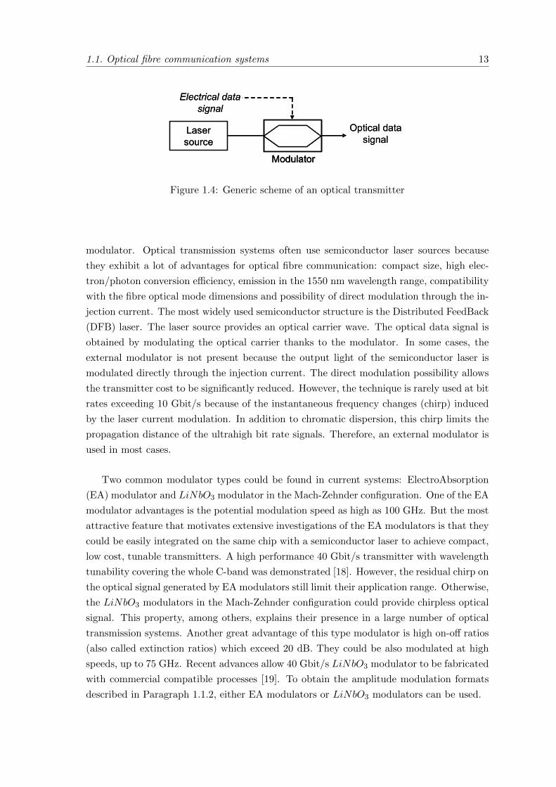
1.1. Optical fibre communication systems 13
Laser source
Electrical data signal
Modulator
Optical data signal
Laser source
Electrical data signal
ModulatorModulator
Optical data signal
Figure 1.4: Generic scheme of an optical transmitter
modulator. Optical transmission systems often use semiconductor laser sources because
they exhibit a lot of advantages for optical fibre communication: compact size, high elec-
tron/photon conversion efficiency, emission in the 1550 nm wavelength range, compatibility
with the fibre optical mode dimensions and possibility of direct modulation through the in-
jection current. The most widely used semiconductor structure is the Distributed FeedBack
(DFB) laser. The laser source provides an optical carrier wave. The optical data signal is
obtained by modulating the optical carrier thanks to the modulator. In some cases, the
external modulator is not present because the output light of the semiconductor laser is
modulated directly through the injection current. The direct modulation possibility allows
the transmitter cost to be significantly reduced. However, the technique is rarely used at bit
rates exceeding 10 Gbit/s because of the instantaneous frequency changes (chirp) induced
by the laser current modulation. In addition to chromatic dispersion, this chirp limits the
propagation distance of the ultrahigh bit rate signals. Therefore, an external modulator is
used in most cases.
Two common modulator types could be found in current systems: ElectroAbsorption
(EA) modulator and LiNbO3 modulator in the Mach-Zehnder configuration. One of the EA
modulator advantages is the potential modulation speed as high as 100 GHz. But the most
attractive feature that motivates extensive investigations of the EA modulators is that they
could be easily integrated on the same chip with a semiconductor laser to achieve compact,
low cost, tunable transmitters. A high performance 40 Gbit/s transmitter with wavelength
tunability covering the whole C-band was demonstrated [18]. However, the residual chirp on
the optical signal generated by EA modulators still limit their application range. Otherwise,
the LiNbO3 modulators in the Mach-Zehnder configuration could provide chirpless optical
signal. This property, among others, explains their presence in a large number of optical
transmission systems. Another great advantage of this type modulator is high on-off ratios
(also called extinction ratios) which exceed 20 dB. They could be also modulated at high
speeds, up to 75 GHz. Recent advances allow 40 Gbit/s LiNbO3 modulator to be fabricated
with commercial compatible processes [19]. To obtain the amplitude modulation formats
described in Paragraph 1.1.2, either EA modulators or LiNbO3 modulators can be used.
14 Chapter 1. Optical fibre communication systems and all-optical regeneration
Low-passfilter
Ampli Decisioncircuit
Clockrecovery
Electricaldata signal
Electrical circuit
Optical data signal
PhotodiodeLow-pass
filter
AmpliAmpli Decisioncircuit
Clockrecovery
Electricaldata signal
Electrical circuit
Optical data signal
Photodiode
Figure 1.5: Generic scheme of a digital optical receiver
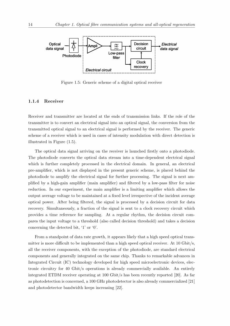
1.1.4 Receiver
Receiver and transmitter are located at the ends of transmission links. If the role of the
transmitter is to convert an electrical signal into an optical signal, the conversion from the
transmitted optical signal to an electrical signal is performed by the receiver. The generic
scheme of a receiver which is used in cases of intensity modulation with direct detection is
illustrated in Figure (1.5).
The optical data signal arriving on the receiver is launched firstly onto a photodiode.
The photodiode converts the optical data stream into a time-dependent electrical signal
which is further completely processed in the electrical domain. In general, an electrical
pre-amplifier, which is not displayed in the present generic scheme, is placed behind the
photodiode to amplify the electrical signal for further processing. The signal is next am-
plified by a high-gain amplifier (main amplifier) and filtered by a low-pass filter for noise
reduction. In our experiment, the main amplifier is a limiting amplifier which allows the
output average voltage to be maintained at a fixed level irrespective of the incident average
optical power. After being filtered, the signal is processed by a decision circuit for data
recovery. Simultaneously, a fraction of the signal is sent to a clock recovery circuit which
provides a time reference for sampling. At a regular rhythm, the decision circuit com-
pares the input voltage to a threshold (also called decision threshold) and takes a decision
concerning the detected bit, ‘1’ or ‘0’.
From a standpoint of data rate growth, it appears likely that a high speed optical trans-
mitter is more difficult to be implemented than a high speed optical receiver. At 10 Gbit/s,
all the receiver components, with the exception of the photodiode, are standard electrical
components and generally integrated on the same chip. Thanks to remarkable advances in
Integrated Circuit (IC) technology developed for high speed microelectronic devices, elec-
tronic circuitry for 40 Gbit/s operations is already commercially available. An entirely
integrated ETDM receiver operating at 100 Gbit/s has been recently reported [20]. As far
as photodetection is concerned, a 100 GHz photodetector is also already commercialized [21]
and photodetector bandwidth keeps increasing [22].
1.1. Optical fibre communication systems 15
t
a)
t
b)t
a)
t
a)
t
b)
t
b)
Figure 1.6: Illustration of an RZ format signal at a transmitter output (a) and the signalafter a long fibre transmission (b)
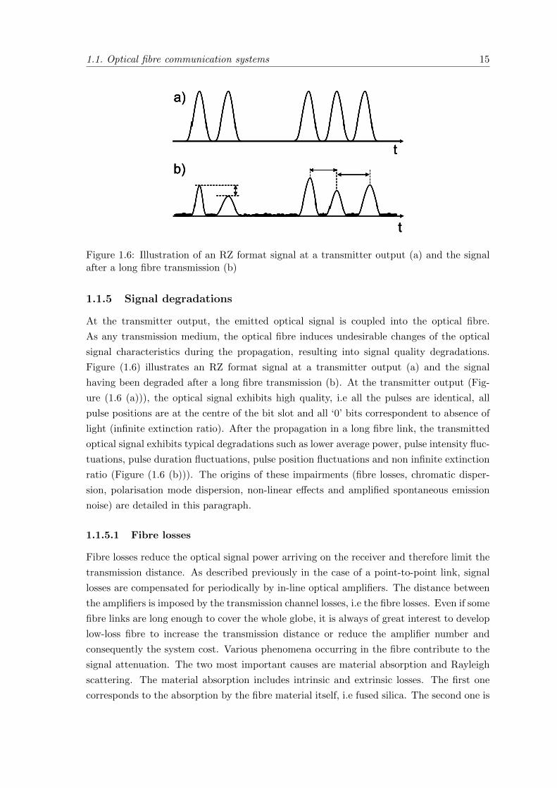
1.1.5 Signal degradations
At the transmitter output, the emitted optical signal is coupled into the optical fibre.
As any transmission medium, the optical fibre induces undesirable changes of the optical
signal characteristics during the propagation, resulting into signal quality degradations.
Figure (1.6) illustrates an RZ format signal at a transmitter output (a) and the signal
having been degraded after a long fibre transmission (b). At the transmitter output (Fig-
ure (1.6 (a))), the optical signal exhibits high quality, i.e all the pulses are identical, all
pulse positions are at the centre of the bit slot and all ‘0’ bits correspondent to absence of
light (infinite extinction ratio). After the propagation in a long fibre link, the transmitted
optical signal exhibits typical degradations such as lower average power, pulse intensity fluc-
tuations, pulse duration fluctuations, pulse position fluctuations and non infinite extinction
ratio (Figure (1.6 (b))). The origins of these impairments (fibre losses, chromatic disper-
sion, polarisation mode dispersion, non-linear effects and amplified spontaneous emission
noise) are detailed in this paragraph.
1.1.5.1 Fibre losses
Fibre losses reduce the optical signal power arriving on the receiver and therefore limit the
transmission distance. As described previously in the case of a point-to-point link, signal
losses are compensated for periodically by in-line optical amplifiers. The distance between
the amplifiers is imposed by the transmission channel losses, i.e the fibre losses. Even if some
fibre links are long enough to cover the whole globe, it is always of great interest to develop
low-loss fibre to increase the transmission distance or reduce the amplifier number and
consequently the system cost. Various phenomena occurring in the fibre contribute to the
signal attenuation. The two most important causes are material absorption and Rayleigh
scattering. The material absorption includes intrinsic and extrinsic losses. The first one
corresponds to the absorption by the fibre material itself, i.e fused silica. The second one is
16 Chapter 1. Optical fibre communication systems and all-optical regeneration
Figure 1.7: Attenuation of a single-mode fibre versus wavelength (reprinted from [1])
due to the presence of impurities. The fibre imperfections and bends constitute also other
sources of losses.
The fibre losses depend on the wavelength of the transmitted light. Figure (1.7) reprinted
from [1] displays the attenuation of a single mode fibre versus the wavelength. The fibre
exhibits a loss of only 0.2 dB/km in the wavelength region near 1.55 µm. This is the
explanation of the 1.55 µm wavelength region choice for telecommunications. The two
attenuation peaks around 1.24 µm and 1.4 µm correspond to the resonances of the OH ion.
The curve of Figure (1.7) is representative for typical current Single-Mode Fibres (SMF)
today.
In general, the losses of a fibre are represented by a global loss parameter called at-
tenuation coefficient. The power of the optical signal propagating in a fibre decreases
exponentially with the distance. The signal attenuation is governed by Equation (1-1).
Pout (L) = Pin (0) exp (−αL) (1-1)
where α is the attenuation coefficient of the optical fibre. It is commonly referred in dB/km
and deduced by using Equation (1-2).
a (dB/km) = −10
Llog10
(PoutPin
)(1-2)
Even if the attenuation coefficient is as low as 0.2 dB/km, a 100 km link exhibits an attenu-
ation of 20 dB. It is clear that the fibre losses are the first source of signal degradations. In
the undersea systems connecting North America and Europe, optical amplifiers are inserted
every 50 km to compensate for the signal attenuation [17].
1.1. Optical fibre communication systems 17
t
I
z
t
t
t
t
I
z
t
t
t
Figure 1.8: Description of pulse broadening due to chromatic dispersion
1.1.5.2 Chromatic dispersion
On one hand, the refractive index of any material, in particular the fused silica, is wavelength-
dependent. The phenomenon is called chromatic dispersion or Group Velocity Dispersion
(GVD). It implies that signals at different wavelengths (or frequencies) propagate at differ-
ent velocities in an optical fibre. On the other hand, no optical signal is ideally monochro-
matic, it has always a finite spectral bandwidth. Thus, the different spectral components
of the transmitted optical signal slide far from each other as the propagation distance in-
creases. In an SMF, the spectral components of the pulse at short wavelengths travel faster
than those at longer wavelengths. The chromatic dispersion impacts on system perfor-
mance by broadening the propagating pulses as described in Figure (1.8). When the pulse
broadening is large enough, the unwanted phenomenon - intersymbol interference (ISI), i.e
pulse overlapping, takes place. For a typical single-mode fibre, the chromatic dispersion is
mainly due to the material dispersion and the modal dispersion. The material dispersion
represents the intrinsic wavelength-dependent of the material refractive index. The modal
dispersion represents the wavelength-dependent of the propagation constant of the guided
modes.
The chromatic dispersion of a conventional SMF fibre and the relative contributions of
the material and modal dispersions are depicted in Figure (1.9). The dispersion parameter
D is expressed in ps/nm/km. In the 1.55 µm window, D is about 17 ps/nm/km. The
dispersion parameter cancels around 1.3 µm.
If the spectral width of the emitted signal is given, the pulse broadening can be estimated
at any transmission distance. The chromatic dispersion imposes a limit on the maximum
transmission distance without signal regenerating. A specific distance called dispersion
length is defined by Equation (1-3).
LD =T 20
|β2|(1-3)
with T0 and β2 are respectively the pulse duration and the second-order dispersion at the
18 Chapter 1. Optical fibre communication systems and all-optical regeneration
Figure 1.9: Total dispersion parameter D and relative contributions of material dispersionDM and waveguide dispersion DW for a conventional single mode fibre (reprinted from [2])
signal wavelength. If a Gaussian pulse is considered, LD is the transmission distance at
which the pulse has broadened by a factor of√
2. Equation (1-3) indicates also that when
the data rate increases, the dispersion length decreases rapidly because the pulse duration
is shorter. Similar to the signal degradations caused by the fibre losses, it appears clearly
that the signal degradations caused by the chromatic dispersion have to be compensated
for in high bit rate systems. The conventional fibre exhibits unfortunately zero dispersion
at 1.3 µm and not at 1.55 µm. However, fibres exhibiting zero or nearly zero dispersion
at 1.55 µm called Dispersion Shifted Fibre (DSF) and Non Zero Dispersion Shifted Fibre
(NZ-DSF) are available. They are designed such that the modal contribution to the total
chromatic dispersion compensates for the material contribution and the zero dispersion is
shifted to an expected wavelength in 1.55 µm region. Although the use of these fibres
will enhance significantly the system performance, non-linear effects such as FWM occur
easily and become drawbacks for WDM systems. Hence, most of current links deploy
conventional single mode fibres. Another technique to mitigate the signal degradations
caused by the chromatic dispersion is using Dispersion Compensating Fibres (DCF). A
DCF is a single-mode fibre exhibiting negative dispersion. The dispersion induced by an
L-length conventional fibre (D is positive around 1.55 µm) could be compensated for by
using a DCF fibre with a length of LDCF which satisfies Equation (1-4).
LSMF ×DSMF = LDCF ×DDCF (1-4)
1.1. Optical fibre communication systems 19
τ∆
Fibre principal axes
Incident polarisation orientation τ∆ τ∆
Fibre principal axes
Incident polarisation orientation
Figure 1.10: Illustration of PMD effect in a polarisation-maintaining fibre
1.1.5.3 Polarisation Mode Dispersion
Optical fibres are not ideally isotropic. They exhibit a non-zero birefringence. The sources
of the fibre birefringence can be divided into two categories: intrinsic birefringence and
extrinsic birefringence induced by environmental factors. The intrinsic birefringence is in-
troduced during the manufacturing process and is due to noncircular core, non-symmetrical
stress around the core region, etc... The environmental factors such as outside fibre stress,
bends, constraints, etc... induce the extrinsic birefringence. The fibre birefringence makes
that the two polarisation modes corresponding to the two principal axes of the fibre propa-
gate with different group velocities. The phenomenon is called Polarisation Mode Dispersion
(PMD). For a polarisation-maintaining fibre without external mechanic stress, the PMD
effect could be naively described by a delay ∆τ between the two polarisation modes as
shown in Figure (1.10). ∆τ is commonly called Differential Group Delay (DGD) and in
that case, it is calculated by using Equation (1-5).
∆τ =L∆neff
c(1-5)
with L is the fibre length, c is the light velocity in vacuum and ∆neff is the difference
between effective index corresponding to the fibre principal axes. In a conventional single
mode fibre, the PMD effect is much more complicated than that described in Figure (1.10)
because the two principal axes change randomly along the fibre. The PMD effect results
firstly in pulse broadening. Figure (1.11) displayed experimental eye diagrams of a 40 Gbit/s
RZ format signal which has the two polarisation states exhibiting a DGD of 0 ps in one
case and of 14 ps in the other case. It is observed that the eye diagrams in the second case
are strongly distorted.
In practice, the signal degradations induced by the PMD is very difficult to be com-
pensated for because the PMD effect is a random process. The signal polarisation changes
randomly during the propagation because of the random variations of the perturbations
along the fibre. In the current long haul transmission systems where the base bit rates do
not exceed 10 Gbit/s yet, the optical pulse broadening induced by the PMD is still small
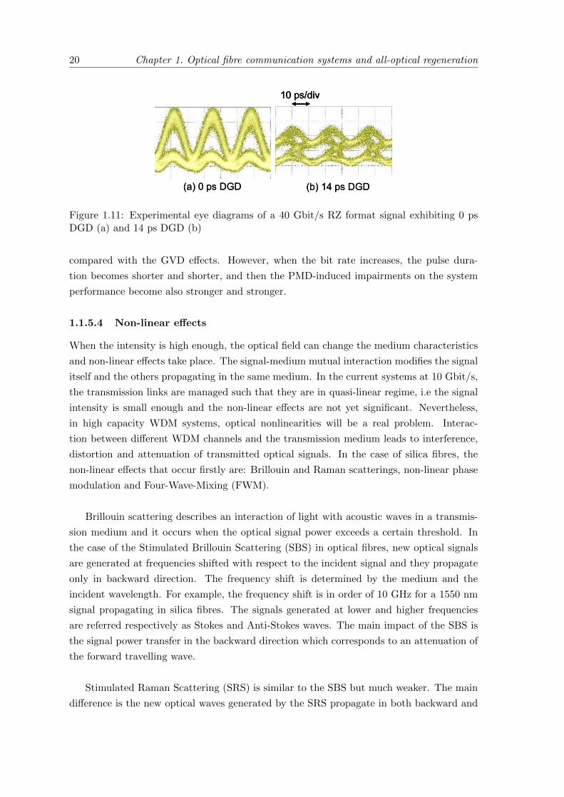
20 Chapter 1. Optical fibre communication systems and all-optical regeneration
10 ps/div
(a) 0 ps DGD (b) 14 ps DGD
10 ps/div10 ps/div
(a) 0 ps DGD (b) 14 ps DGD
Figure 1.11: Experimental eye diagrams of a 40 Gbit/s RZ format signal exhibiting 0 psDGD (a) and 14 ps DGD (b)
compared with the GVD effects. However, when the bit rate increases, the pulse dura-
tion becomes shorter and shorter, and then the PMD-induced impairments on the system
performance become also stronger and stronger.
1.1.5.4 Non-linear effects
When the intensity is high enough, the optical field can change the medium characteristics
and non-linear effects take place. The signal-medium mutual interaction modifies the signal
itself and the others propagating in the same medium. In the current systems at 10 Gbit/s,
the transmission links are managed such that they are in quasi-linear regime, i.e the signal
intensity is small enough and the non-linear effects are not yet significant. Nevertheless,
in high capacity WDM systems, optical nonlinearities will be a real problem. Interac-
tion between different WDM channels and the transmission medium leads to interference,
distortion and attenuation of transmitted optical signals. In the case of silica fibres, the
non-linear effects that occur firstly are: Brillouin and Raman scatterings, non-linear phase
modulation and Four-Wave-Mixing (FWM).
Brillouin scattering describes an interaction of light with acoustic waves in a transmis-
sion medium and it occurs when the optical signal power exceeds a certain threshold. In
the case of the Stimulated Brillouin Scattering (SBS) in optical fibres, new optical signals
are generated at frequencies shifted with respect to the incident signal and they propagate
only in backward direction. The frequency shift is determined by the medium and the
incident wavelength. For example, the frequency shift is in order of 10 GHz for a 1550 nm
signal propagating in silica fibres. The signals generated at lower and higher frequencies
are referred respectively as Stokes and Anti-Stokes waves. The main impact of the SBS is
the signal power transfer in the backward direction which corresponds to an attenuation of
the forward travelling wave.
Stimulated Raman Scattering (SRS) is similar to the SBS but much weaker. The main
difference is the new optical waves generated by the SRS propagate in both backward and
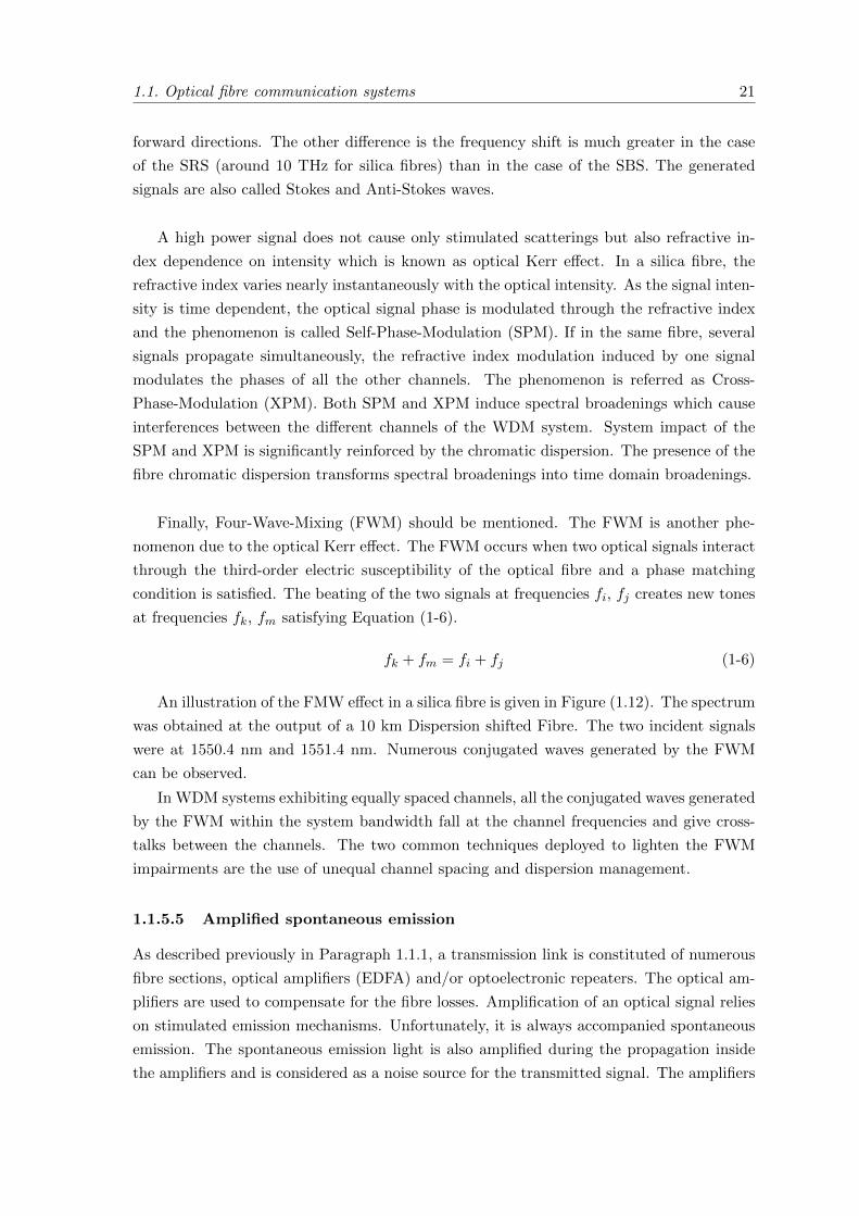
1.1. Optical fibre communication systems 21
forward directions. The other difference is the frequency shift is much greater in the case
of the SRS (around 10 THz for silica fibres) than in the case of the SBS. The generated
signals are also called Stokes and Anti-Stokes waves.
A high power signal does not cause only stimulated scatterings but also refractive in-
dex dependence on intensity which is known as optical Kerr effect. In a silica fibre, the
refractive index varies nearly instantaneously with the optical intensity. As the signal inten-
sity is time dependent, the optical signal phase is modulated through the refractive index
and the phenomenon is called Self-Phase-Modulation (SPM). If in the same fibre, several
signals propagate simultaneously, the refractive index modulation induced by one signal
modulates the phases of all the other channels. The phenomenon is referred as Cross-
Phase-Modulation (XPM). Both SPM and XPM induce spectral broadenings which cause
interferences between the different channels of the WDM system. System impact of the
SPM and XPM is significantly reinforced by the chromatic dispersion. The presence of the
fibre chromatic dispersion transforms spectral broadenings into time domain broadenings.
Finally, Four-Wave-Mixing (FWM) should be mentioned. The FWM is another phe-
nomenon due to the optical Kerr effect. The FWM occurs when two optical signals interact
through the third-order electric susceptibility of the optical fibre and a phase matching
condition is satisfied. The beating of the two signals at frequencies fi, fj creates new tones
at frequencies fk, fm satisfying Equation (1-6).
fk + fm = fi + fj (1-6)
An illustration of the FMW effect in a silica fibre is given in Figure (1.12). The spectrum
was obtained at the output of a 10 km Dispersion shifted Fibre. The two incident signals
were at 1550.4 nm and 1551.4 nm. Numerous conjugated waves generated by the FWM
can be observed.
In WDM systems exhibiting equally spaced channels, all the conjugated waves generated
by the FWM within the system bandwidth fall at the channel frequencies and give cross-
talks between the channels. The two common techniques deployed to lighten the FWM
impairments are the use of unequal channel spacing and dispersion management.
1.1.5.5 Amplified spontaneous emission
As described previously in Paragraph 1.1.1, a transmission link is constituted of numerous
fibre sections, optical amplifiers (EDFA) and/or optoelectronic repeaters. The optical am-
plifiers are used to compensate for the fibre losses. Amplification of an optical signal relies
on stimulated emission mechanisms. Unfortunately, it is always accompanied spontaneous
emission. The spontaneous emission light is also amplified during the propagation inside
the amplifiers and is considered as a noise source for the transmitted signal. The amplifiers
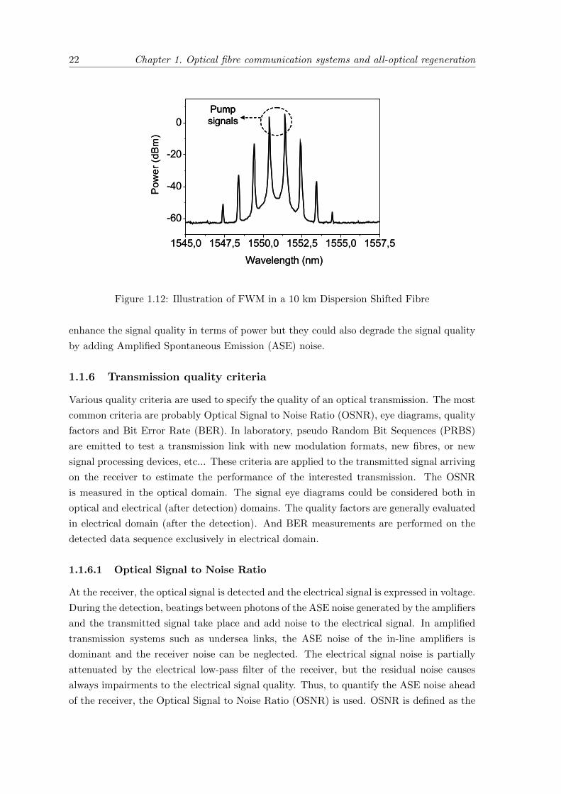
22 Chapter 1. Optical fibre communication systems and all-optical regeneration
1545,0 1547,5 1550,0 1552,5 1555,0 1557,5
-60
-40
-20
0
Pow
er (d
Bm
)
Wavelength (nm)
Pump signals
1545,0 1547,5 1550,0 1552,5 1555,0 1557,5
-60
-40
-20
0
Pow
er (d
Bm
)
Wavelength (nm)
Pump signalsPump signals
Figure 1.12: Illustration of FWM in a 10 km Dispersion Shifted Fibre
enhance the signal quality in terms of power but they could also degrade the signal quality
by adding Amplified Spontaneous Emission (ASE) noise.
1.1.6 Transmission quality criteria
Various quality criteria are used to specify the quality of an optical transmission. The most
common criteria are probably Optical Signal to Noise Ratio (OSNR), eye diagrams, quality
factors and Bit Error Rate (BER). In laboratory, pseudo Random Bit Sequences (PRBS)
are emitted to test a transmission link with new modulation formats, new fibres, or new
signal processing devices, etc... These criteria are applied to the transmitted signal arriving
on the receiver to estimate the performance of the interested transmission. The OSNR
is measured in the optical domain. The signal eye diagrams could be considered both in
optical and electrical (after detection) domains. The quality factors are generally evaluated
in electrical domain (after the detection). And BER measurements are performed on the
detected data sequence exclusively in electrical domain.
1.1.6.1 Optical Signal to Noise Ratio
At the receiver, the optical signal is detected and the electrical signal is expressed in voltage.
During the detection, beatings between photons of the ASE noise generated by the amplifiers
and the transmitted signal take place and add noise to the electrical signal. In amplified
transmission systems such as undersea links, the ASE noise of the in-line amplifiers is
dominant and the receiver noise can be neglected. The electrical signal noise is partially
attenuated by the electrical low-pass filter of the receiver, but the residual noise causes
always impairments to the electrical signal quality. Thus, to quantify the ASE noise ahead
of the receiver, the Optical Signal to Noise Ratio (OSNR) is used. OSNR is defined as the
1.1. Optical fibre communication systems 23
-35
-30
-25
-20
-15
-10
-5
0
1540 1542 1544 1546 1548 1550Wavelength (nm)
Pow
er (d
Bm)
Zone1 Zone 2
-35
-30
-25
-20
-15
-10
-5
0
1540 1542 1544 1546 1548 1550Wavelength (nm)
Pow
er (d
Bm)
Zone1 Zone 2
Figure 1.13: Principle of OSNR measurement using OSA
ratio of the signal power to the noise power measured over a given spectral bandwidth and
calculated by using Equation (1-7).
OSNR =PsignalPnoise
(1-7)
The OSNR over a spectral band of width B can be measured by using an Optical
Spectrum Analyser (OSA). Principle of the measurement is described in Figure (1.13).
The power integrated within the signal bandwidth B (zone 1) includes both signal and
noise power contributions and thus corresponds to Psignal + Pnoise. The power integrated
within zone 2 (spectral bandwidth of B) corresponds to the noise power Pnoise only. If the
measured powers are expressed in dBm and the OSNR is expressed in dB, their relations
are given by Equation (1-8).
OSNRdB = 10 log10
(10
(Psignal+Pnoise)dBm−(Pnoise)dBm
10 − 1
)(1-8)
If Psignal >> Pnoise, then ONSR could be approximated by Equation (1-9). However,
this approximation is reliable only if OSNRdB > 13dB.
OSNRdB = (P signal + Pnoise)dBm − (Pnoise)dBm (1-9)
1.1.6.2 Eye diagrams
An eye diagram is the superposition of all the waveforms corresponding to all the possible bit
sequences. In general, signal eye diagrams are achieved in the electrical domain after being
detected by a photodiode, and are observed thanks to an electrical sampling oscilloscope.
The electrical eye diagrams are representative for the optical signal only if the photodiode
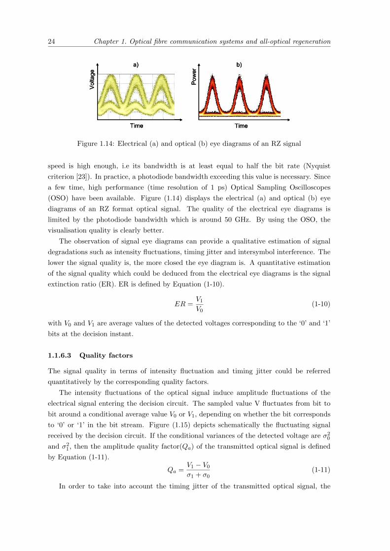
24 Chapter 1. Optical fibre communication systems and all-optical regeneration
Time
Voltage
a)
Time
Power
b)
Time
Voltage
a)
Time
Voltage
a)
Time
Power
b)
Time
Power
b)
Figure 1.14: Electrical (a) and optical (b) eye diagrams of an RZ signal
speed is high enough, i.e its bandwidth is at least equal to half the bit rate (Nyquist
criterion [23]). In practice, a photodiode bandwidth exceeding this value is necessary. Since
a few time, high performance (time resolution of 1 ps) Optical Sampling Oscilloscopes
(OSO) have been available. Figure (1.14) displays the electrical (a) and optical (b) eye
diagrams of an RZ format optical signal. The quality of the electrical eye diagrams is
limited by the photodiode bandwidth which is around 50 GHz. By using the OSO, the
visualisation quality is clearly better.
The observation of signal eye diagrams can provide a qualitative estimation of signal
degradations such as intensity fluctuations, timing jitter and intersymbol interference. The
lower the signal quality is, the more closed the eye diagram is. A quantitative estimation
of the signal quality which could be deduced from the electrical eye diagrams is the signal
extinction ratio (ER). ER is defined by Equation (1-10).
ER =V1V0
(1-10)
with V0 and V1 are average values of the detected voltages corresponding to the ‘0’ and ‘1’
bits at the decision instant.
1.1.6.3 Quality factors
The signal quality in terms of intensity fluctuation and timing jitter could be referred
quantitatively by the corresponding quality factors.
The intensity fluctuations of the optical signal induce amplitude fluctuations of the
electrical signal entering the decision circuit. The sampled value V fluctuates from bit to
bit around a conditional average value V0 or V1, depending on whether the bit corresponds
to ‘0’ or ‘1’ in the bit stream. Figure (1.15) depicts schematically the fluctuating signal
received by the decision circuit. If the conditional variances of the detected voltage are σ20and σ21, then the amplitude quality factor(Qa) of the transmitted optical signal is defined
by Equation (1-11).
Qa =V1 − V0σ1 + σ0
(1-11)
In order to take into account the timing jitter of the transmitted optical signal, the
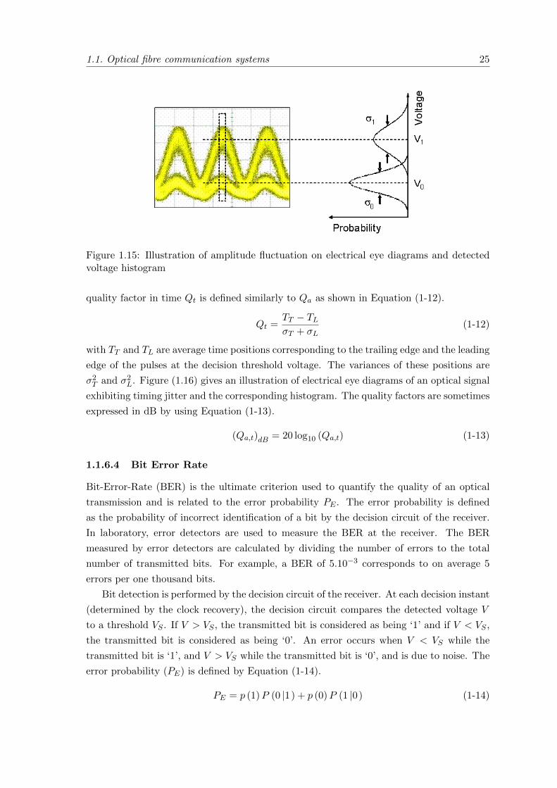
1.1. Optical fibre communication systems 25
Figure 1.15: Illustration of amplitude fluctuation on electrical eye diagrams and detectedvoltage histogram
quality factor in time Qt is defined similarly to Qa as shown in Equation (1-12).
Qt =TT − TLσT + σL
(1-12)
with TT and TL are average time positions corresponding to the trailing edge and the leading
edge of the pulses at the decision threshold voltage. The variances of these positions are
σ2T and σ2L. Figure (1.16) gives an illustration of electrical eye diagrams of an optical signal
exhibiting timing jitter and the corresponding histogram. The quality factors are sometimes
expressed in dB by using Equation (1-13).
(Qa,t)dB = 20 log10 (Qa,t) (1-13)
1.1.6.4 Bit Error Rate
Bit-Error-Rate (BER) is the ultimate criterion used to quantify the quality of an optical
transmission and is related to the error probability PE . The error probability is defined
as the probability of incorrect identification of a bit by the decision circuit of the receiver.
In laboratory, error detectors are used to measure the BER at the receiver. The BER
measured by error detectors are calculated by dividing the number of errors to the total
number of transmitted bits. For example, a BER of 5.10−3 corresponds to on average 5
errors per one thousand bits.
Bit detection is performed by the decision circuit of the receiver. At each decision instant
(determined by the clock recovery), the decision circuit compares the detected voltage V
to a threshold VS . If V > VS , the transmitted bit is considered as being ‘1’ and if V < VS ,
the transmitted bit is considered as being ‘0’. An error occurs when V < VS while the
transmitted bit is ‘1’, and V > VS while the transmitted bit is ‘0’, and is due to noise. The
error probability (PE) is defined by Equation (1-14).
PE = p (1)P (0 |1) + p (0)P (1 |0) (1-14)
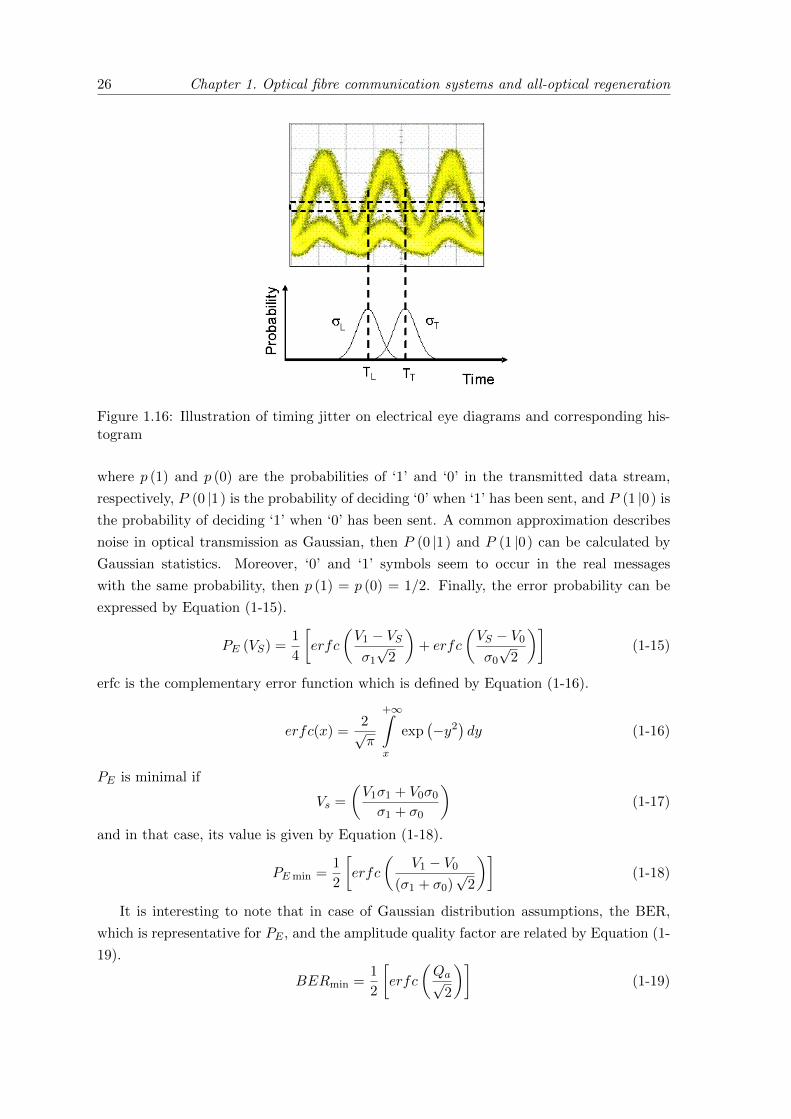
26 Chapter 1. Optical fibre communication systems and all-optical regeneration
Figure 1.16: Illustration of timing jitter on electrical eye diagrams and corresponding his-togram
where p (1) and p (0) are the probabilities of ‘1’ and ‘0’ in the transmitted data stream,
respectively, P (0 |1) is the probability of deciding ‘0’ when ‘1’ has been sent, and P (1 |0) is
the probability of deciding ‘1’ when ‘0’ has been sent. A common approximation describes
noise in optical transmission as Gaussian, then P (0 |1) and P (1 |0) can be calculated by
Gaussian statistics. Moreover, ‘0’ and ‘1’ symbols seem to occur in the real messages
with the same probability, then p (1) = p (0) = 1/2. Finally, the error probability can be
expressed by Equation (1-15).
PE (VS) =1
4
[erfc
(V1 − VSσ1√
2
)+ erfc
(VS − V0σ0√
2
)](1-15)
erfc is the complementary error function which is defined by Equation (1-16).
erfc(x) =2√π
+∞∫x
exp(−y2
)dy (1-16)
PE is minimal if
Vs =
(V1σ1 + V0σ0σ1 + σ0
)(1-17)
and in that case, its value is given by Equation (1-18).
PEmin =1
2
[erfc
(V1 − V0
(σ1 + σ0)√
2
)](1-18)
It is interesting to note that in case of Gaussian distribution assumptions, the BER,
which is representative for PE , and the amplitude quality factor are related by Equation (1-
19).
BERmin =1
2
[erfc
(Qa√
2
)](1-19)
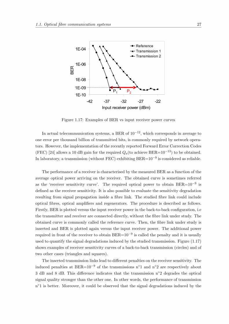
1.1. Optical fibre communication systems 27
1E-10
1E-08
1E-06
1E-04
-42 -37 -32 -27 -22Input receiver power (dBm)
BER
ReferenceTransmission 1Transmission 2
P11E-09
P21E-10
1E-08
1E-06
1E-04
-42 -37 -32 -27 -22Input receiver power (dBm)
BER
ReferenceTransmission 1Transmission 2
P11E-09
P2
Figure 1.17: Examples of BER vs input receiver power curves
In actual telecommunication systems, a BER of 10−12, which corresponds in average to
one error per thousand billion of transmitted bits, is commonly required by network opera-
tors. However, the implementation of the recently reported Forward Error Correction Codes
(FEC) [24] allows a 10 dB gain for the required Qa(to achieve BER=10−13) to be obtained.
In laboratory, a transmission (without FEC) exhibiting BER=10−9 is considered as reliable.
The performance of a receiver is characterised by the measured BER as a function of the
average optical power arriving on the receiver. The obtained curve is sometimes referred
as the ‘receiver sensitivity curve’. The required optical power to obtain BER=10−9 is
defined as the receiver sensitivity. It is also possible to evaluate the sensitivity degradation
resulting from signal propagation inside a fibre link. The studied fibre link could include
optical fibres, optical amplifiers and regenerators. The procedure is described as follows.
Firstly, BER is plotted versus the input receiver power in the back-to-back configuration, i.e
the transmitter and receiver are connected directly, without the fibre link under study. The
obtained curve is commonly called the reference curve. Then, the fibre link under study is
inserted and BER is plotted again versus the input receiver power. The additional power
required in front of the receiver to obtain BER=10−9 is called the penalty and it is usually
used to quantify the signal degradations induced by the studied transmission. Figure (1.17)
shows examples of receiver sensitivity curves of a back-to-back transmission (circles) and of
two other cases (triangles and squares).
The inserted transmission links lead to different penalties on the receiver sensitivity. The
induced penalties at BER=10−9 of the transmissions n◦1 and n◦2 are respectively about
3 dB and 8 dB. This difference indicates that the transmission n◦2 degrades the optical
signal quality stronger than the other one. In other words, the performance of transmission
n◦1 is better. Moreover, it could be observed that the signal degradations induced by the

28 Chapter 1. Optical fibre communication systems and all-optical regeneration
transmission n◦2 are so important that the BER of 10−10 would be unreachable because an
error floor appears at a BER superior to 10−10.
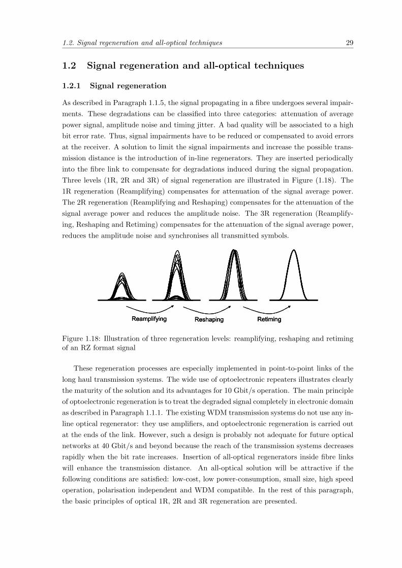
1.2. Signal regeneration and all-optical techniques 29
1.2 Signal regeneration and all-optical techniques
1.2.1 Signal regeneration
As described in Paragraph 1.1.5, the signal propagating in a fibre undergoes several impair-
ments. These degradations can be classified into three categories: attenuation of average
power signal, amplitude noise and timing jitter. A bad quality will be associated to a high
bit error rate. Thus, signal impairments have to be reduced or compensated to avoid errors
at the receiver. A solution to limit the signal impairments and increase the possible trans-
mission distance is the introduction of in-line regenerators. They are inserted periodically
into the fibre link to compensate for degradations induced during the signal propagation.
Three levels (1R, 2R and 3R) of signal regeneration are illustrated in Figure (1.18). The
1R regeneration (Reamplifying) compensates for attenuation of the signal average power.
The 2R regeneration (Reamplifying and Reshaping) compensates for the attenuation of the
signal average power and reduces the amplitude noise. The 3R regeneration (Reamplify-
ing, Reshaping and Retiming) compensates for the attenuation of the signal average power,
reduces the amplitude noise and synchronises all transmitted symbols.
Reamplifying Reshaping RetimingReamplifyingReamplifying ReshapingReshaping RetimingRetiming
Figure 1.18: Illustration of three regeneration levels: reamplifying, reshaping and retimingof an RZ format signal
These regeneration processes are especially implemented in point-to-point links of the
long haul transmission systems. The wide use of optoelectronic repeaters illustrates clearly
the maturity of the solution and its advantages for 10 Gbit/s operation. The main principle
of optoelectronic regeneration is to treat the degraded signal completely in electronic domain
as described in Paragraph 1.1.1. The existing WDM transmission systems do not use any in-
line optical regenerator: they use amplifiers, and optoelectronic regeneration is carried out
at the ends of the link. However, such a design is probably not adequate for future optical
networks at 40 Gbit/s and beyond because the reach of the transmission systems decreases
rapidly when the bit rate increases. Insertion of all-optical regenerators inside fibre links
will enhance the transmission distance. An all-optical solution will be attractive if the
following conditions are satisfied: low-cost, low power-consumption, small size, high speed
operation, polarisation independent and WDM compatible. In the rest of this paragraph,
the basic principles of optical 1R, 2R and 3R regeneration are presented.
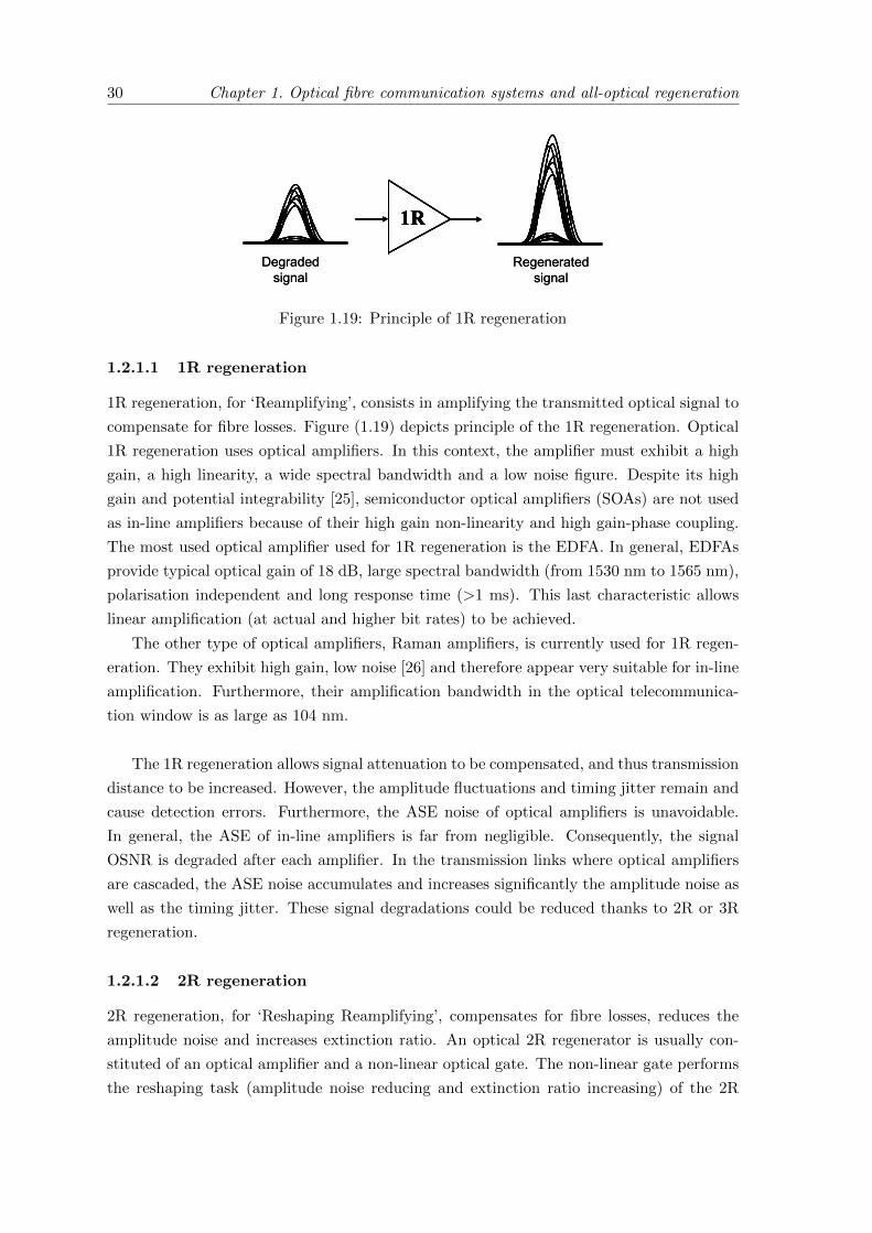
30 Chapter 1. Optical fibre communication systems and all-optical regeneration
1R
Degraded signal
Regenerated signal
1R1R1R
Degraded signal
Regenerated signal
Figure 1.19: Principle of 1R regeneration
1.2.1.1 1R regeneration
1R regeneration, for ‘Reamplifying’, consists in amplifying the transmitted optical signal to
compensate for fibre losses. Figure (1.19) depicts principle of the 1R regeneration. Optical
1R regeneration uses optical amplifiers. In this context, the amplifier must exhibit a high
gain, a high linearity, a wide spectral bandwidth and a low noise figure. Despite its high
gain and potential integrability [25], semiconductor optical amplifiers (SOAs) are not used
as in-line amplifiers because of their high gain non-linearity and high gain-phase coupling.
The most used optical amplifier used for 1R regeneration is the EDFA. In general, EDFAs
provide typical optical gain of 18 dB, large spectral bandwidth (from 1530 nm to 1565 nm),
polarisation independent and long response time (>1 ms). This last characteristic allows
linear amplification (at actual and higher bit rates) to be achieved.
The other type of optical amplifiers, Raman amplifiers, is currently used for 1R regen-
eration. They exhibit high gain, low noise [26] and therefore appear very suitable for in-line
amplification. Furthermore, their amplification bandwidth in the optical telecommunica-
tion window is as large as 104 nm.
The 1R regeneration allows signal attenuation to be compensated, and thus transmission
distance to be increased. However, the amplitude fluctuations and timing jitter remain and
cause detection errors. Furthermore, the ASE noise of optical amplifiers is unavoidable.
In general, the ASE of in-line amplifiers is far from negligible. Consequently, the signal
OSNR is degraded after each amplifier. In the transmission links where optical amplifiers
are cascaded, the ASE noise accumulates and increases significantly the amplitude noise as
well as the timing jitter. These signal degradations could be reduced thanks to 2R or 3R
regeneration.
1.2.1.2 2R regeneration
2R regeneration, for ‘Reshaping Reamplifying’, compensates for fibre losses, reduces the
amplitude noise and increases extinction ratio. An optical 2R regenerator is usually con-
stituted of an optical amplifier and a non-linear optical gate. The non-linear gate performs
the reshaping task (amplitude noise reducing and extinction ratio increasing) of the 2R
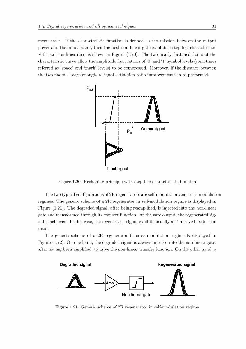
1.2. Signal regeneration and all-optical techniques 31
regenerator. If the characteristic function is defined as the relation between the output
power and the input power, then the best non-linear gate exhibits a step-like characteristic
with two non-linearities as shown in Figure (1.20). The two nearly flattened floors of the
characteristic curve allow the amplitude fluctuations of ‘0’ and ‘1’ symbol levels (sometimes
referred as ‘space’ and ‘mark’ levels) to be compressed. Moreover, if the distance between
the two floors is large enough, a signal extinction ratio improvement is also performed.
Pout
Pin
Input signal
Output signal
Pout
Pin
Input signal
Output signal
Figure 1.20: Reshaping principle with step-like characteristic function
The two typical configurations of 2R regenerators are self-modulation and cross-modulation
regimes. The generic scheme of a 2R regenerator in self-modulation regime is displayed in
Figure (1.21). The degraded signal, after being reamplified, is injected into the non-linear
gate and transformed through its transfer function. At the gate output, the regenerated sig-
nal is achieved. In this case, the regenerated signal exhibits usually an improved extinction
ratio.
The generic scheme of a 2R regenerator in cross-modulation regime is displayed in
Figure (1.22). On one hand, the degraded signal is always injected into the non-linear gate,
after having been amplified, to drive the non-linear transfer function. On the other hand, a
Regenerated signal
Non-linear gate
Ampli
Degraded signal Regenerated signal
Non-linear gate
Ampli
Degraded signalDegraded signal
Figure 1.21: Generic scheme of 2R regenerator in self-modulation regime
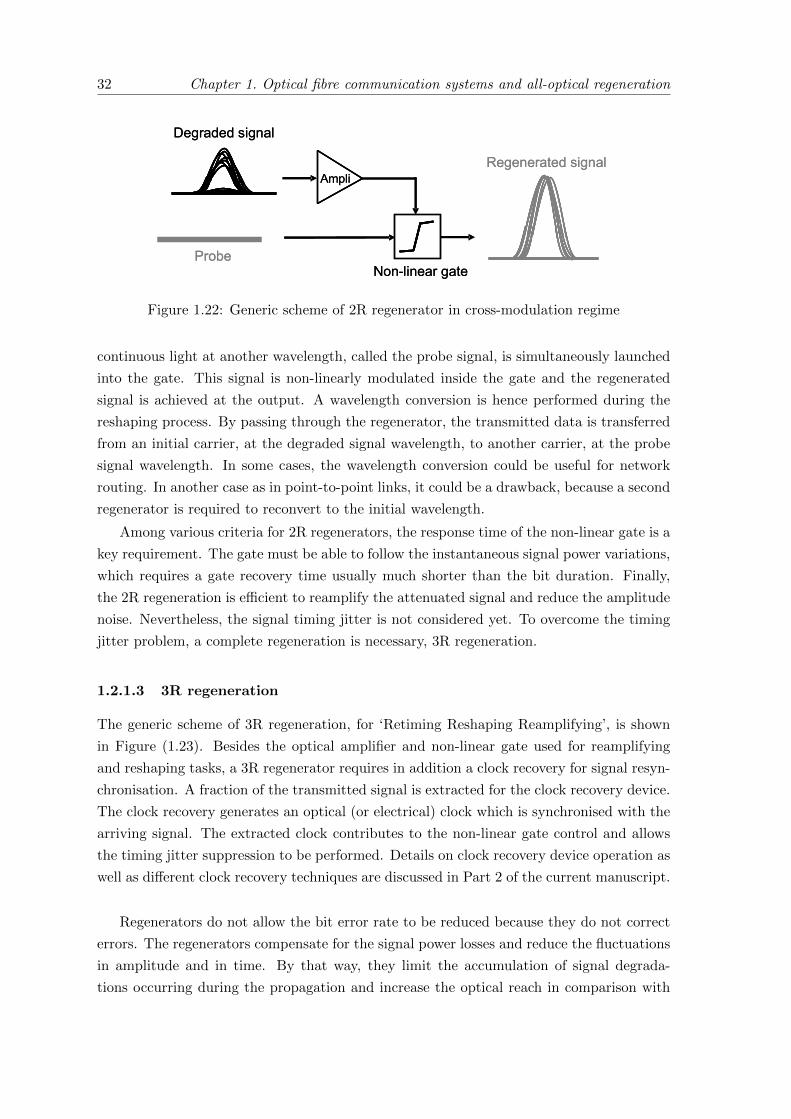
32 Chapter 1. Optical fibre communication systems and all-optical regeneration
Regenerated signal
ProbeNon-linear gate
Ampli
Degraded signal
Regenerated signal
ProbeNon-linear gate
Ampli
Degraded signal
Figure 1.22: Generic scheme of 2R regenerator in cross-modulation regime
continuous light at another wavelength, called the probe signal, is simultaneously launched
into the gate. This signal is non-linearly modulated inside the gate and the regenerated
signal is achieved at the output. A wavelength conversion is hence performed during the
reshaping process. By passing through the regenerator, the transmitted data is transferred
from an initial carrier, at the degraded signal wavelength, to another carrier, at the probe
signal wavelength. In some cases, the wavelength conversion could be useful for network
routing. In another case as in point-to-point links, it could be a drawback, because a second
regenerator is required to reconvert to the initial wavelength.
Among various criteria for 2R regenerators, the response time of the non-linear gate is a
key requirement. The gate must be able to follow the instantaneous signal power variations,
which requires a gate recovery time usually much shorter than the bit duration. Finally,
the 2R regeneration is efficient to reamplify the attenuated signal and reduce the amplitude
noise. Nevertheless, the signal timing jitter is not considered yet. To overcome the timing
jitter problem, a complete regeneration is necessary, 3R regeneration.
1.2.1.3 3R regeneration
The generic scheme of 3R regeneration, for ‘Retiming Reshaping Reamplifying’, is shown
in Figure (1.23). Besides the optical amplifier and non-linear gate used for reamplifying
and reshaping tasks, a 3R regenerator requires in addition a clock recovery for signal resyn-
chronisation. A fraction of the transmitted signal is extracted for the clock recovery device.
The clock recovery generates an optical (or electrical) clock which is synchronised with the
arriving signal. The extracted clock contributes to the non-linear gate control and allows
the timing jitter suppression to be performed. Details on clock recovery device operation as
well as different clock recovery techniques are discussed in Part 2 of the current manuscript.
Regenerators do not allow the bit error rate to be reduced because they do not correct
errors. The regenerators compensate for the signal power losses and reduce the fluctuations
in amplitude and in time. By that way, they limit the accumulation of signal degrada-
tions occurring during the propagation and increase the optical reach in comparison with
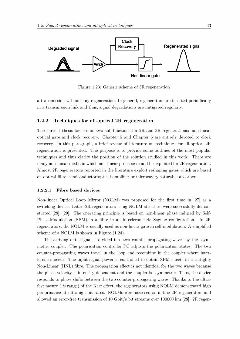
1.2. Signal regeneration and all-optical techniques 33
Regenerated signal
Non-linear gate
Ampli
Clock RecoveryDegraded signal Regenerated signal
Non-linear gate
AmpliAmpliAmpli
Clock RecoveryDegraded signalDegraded signal
Figure 1.23: Generic scheme of 3R regeneration
a transmission without any regeneration. In general, regenerators are inserted periodically
in a transmission link and thus, signal degradations are mitigated regularly.
1.2.2 Techniques for all-optical 2R regeneration
The current thesis focuses on two sub-functions for 2R and 3R regenerations: non-linear
optical gate and clock recovery. Chapter 5 and Chapter 6 are entirely devoted to clock
recovery. In this paragraph, a brief review of literature on techniques for all-optical 2R
regeneration is presented. The purpose is to provide some outlines of the most popular
techniques and thus clarify the position of the solution studied in this work. There are
many non-linear media in which non-linear processes could be exploited for 2R regeneration.
Almost 2R regenerators reported in the literature exploit reshaping gates which are based
on optical fibre, semiconductor optical amplifier or microcavity saturable absorber.
1.2.2.1 Fibre based devices
Non-linear Optical Loop Mirror (NOLM) was proposed for the first time in [27] as a
switching device. Later, 2R regenerators using NOLM structure were successfully demon-
strated [28], [29]. The operating principle is based on non-linear phase induced by Self-
Phase-Modulation (SPM) in a fibre in an interferometric Sagnac configuration. In 2R
regenerators, the NOLM is usually used as non-linear gate in self-modulation. A simplified
scheme of a NOLM is shown in Figure (1.24).
The arriving data signal is divided into two counter-propagating waves by the asym-
metric coupler. The polarisation controller PC adjusts the polarization states. The two
counter-propagating waves travel in the loop and recombine in the coupler where inter-
ferences occur. The input signal power is controlled to obtain SPM effects in the Highly
Non-Linear (HNL) fibre. The propagation effect is not identical for the two waves because
the phase velocity is intensity dependent and the coupler is asymmetric. Thus, the device
responds to phase shifts between the two counter-propagating waves. Thanks to the ultra-
fast nature ( fs range) of the Kerr effect, the regenerators using NOLM demonstrated high
performance at ultrahigh bit rates. NOLMs were assessed as in-line 2R regenerators and
allowed an error-free transmission of 10 Gbit/s bit streams over 100000 km [28]. 2R regen-
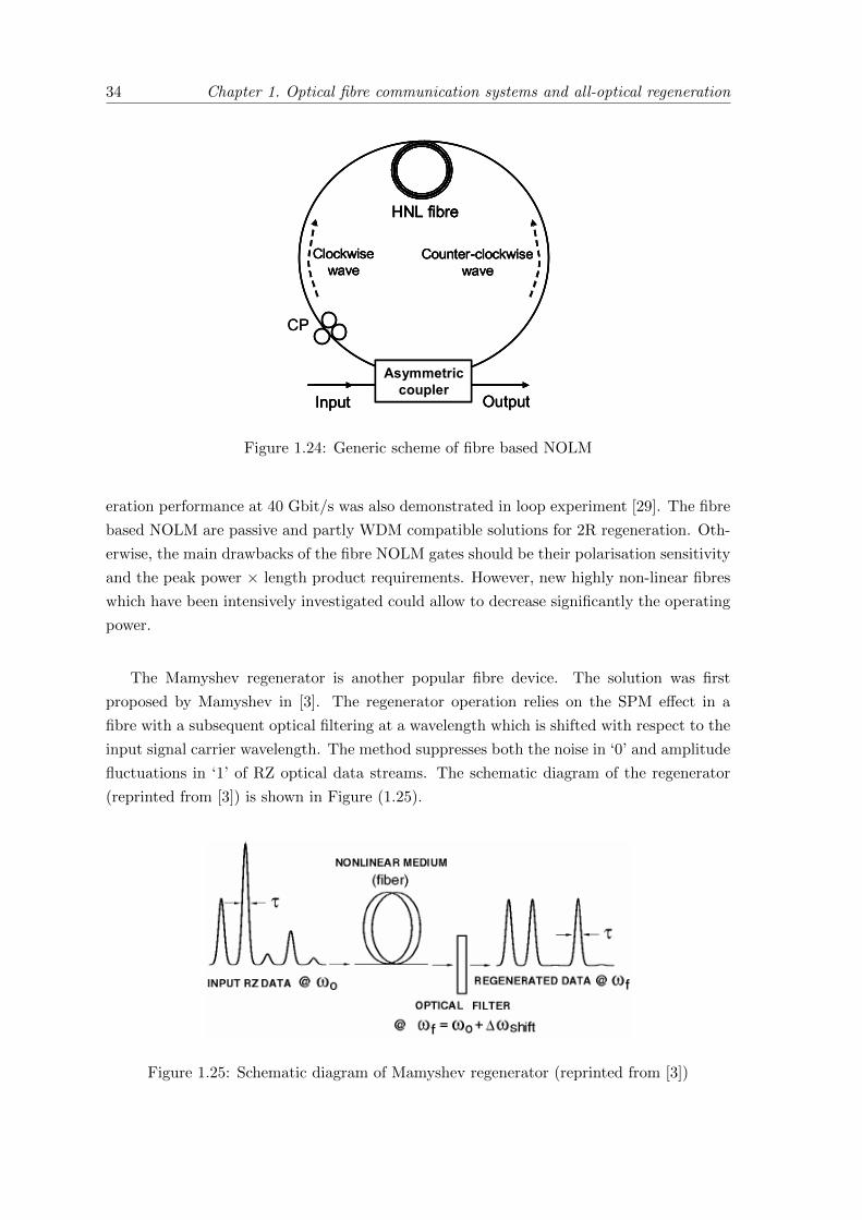
34 Chapter 1. Optical fibre communication systems and all-optical regeneration
Asymmetriccoupler
HNL fibre
Input Output
Clockwisewave
Counter-clockwisewave
CP
Asymmetriccoupler
HNL fibre
Input Output
Clockwisewave
Counter-clockwisewave
Asymmetriccoupler
HNL fibreHNL fibre
Input Output
Clockwisewave
Counter-clockwisewave
CP
Figure 1.24: Generic scheme of fibre based NOLM
eration performance at 40 Gbit/s was also demonstrated in loop experiment [29]. The fibre
based NOLM are passive and partly WDM compatible solutions for 2R regeneration. Oth-
erwise, the main drawbacks of the fibre NOLM gates should be their polarisation sensitivity
and the peak power × length product requirements. However, new highly non-linear fibres
which have been intensively investigated could allow to decrease significantly the operating
power.
The Mamyshev regenerator is another popular fibre device. The solution was first
proposed by Mamyshev in [3]. The regenerator operation relies on the SPM effect in a
fibre with a subsequent optical filtering at a wavelength which is shifted with respect to the
input signal carrier wavelength. The method suppresses both the noise in ‘0’ and amplitude
fluctuations in ‘1’ of RZ optical data streams. The schematic diagram of the regenerator
(reprinted from [3]) is shown in Figure (1.25).
Figure 1.25: Schematic diagram of Mamyshev regenerator (reprinted from [3])
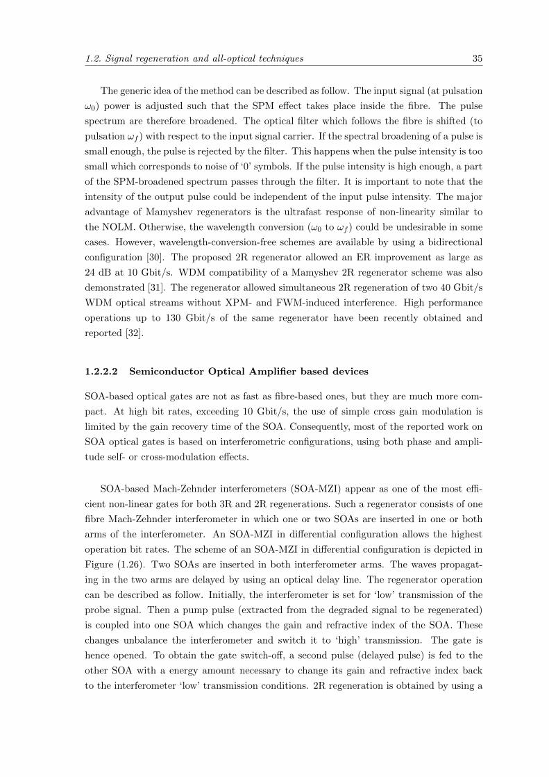
1.2. Signal regeneration and all-optical techniques 35
The generic idea of the method can be described as follow. The input signal (at pulsation
ω0) power is adjusted such that the SPM effect takes place inside the fibre. The pulse
spectrum are therefore broadened. The optical filter which follows the fibre is shifted (to
pulsation ωf ) with respect to the input signal carrier. If the spectral broadening of a pulse is
small enough, the pulse is rejected by the filter. This happens when the pulse intensity is too
small which corresponds to noise of ‘0’ symbols. If the pulse intensity is high enough, a part
of the SPM-broadened spectrum passes through the filter. It is important to note that the
intensity of the output pulse could be independent of the input pulse intensity. The major
advantage of Mamyshev regenerators is the ultrafast response of non-linearity similar to
the NOLM. Otherwise, the wavelength conversion (ω0 to ωf ) could be undesirable in some
cases. However, wavelength-conversion-free schemes are available by using a bidirectional
configuration [30]. The proposed 2R regenerator allowed an ER improvement as large as
24 dB at 10 Gbit/s. WDM compatibility of a Mamyshev 2R regenerator scheme was also
demonstrated [31]. The regenerator allowed simultaneous 2R regeneration of two 40 Gbit/s
WDM optical streams without XPM- and FWM-induced interference. High performance
operations up to 130 Gbit/s of the same regenerator have been recently obtained and
reported [32].
1.2.2.2 Semiconductor Optical Amplifier based devices
SOA-based optical gates are not as fast as fibre-based ones, but they are much more com-
pact. At high bit rates, exceeding 10 Gbit/s, the use of simple cross gain modulation is
limited by the gain recovery time of the SOA. Consequently, most of the reported work on
SOA optical gates is based on interferometric configurations, using both phase and ampli-
tude self- or cross-modulation effects.
SOA-based Mach-Zehnder interferometers (SOA-MZI) appear as one of the most effi-
cient non-linear gates for both 3R and 2R regenerations. Such a regenerator consists of one
fibre Mach-Zehnder interferometer in which one or two SOAs are inserted in one or both
arms of the interferometer. An SOA-MZI in differential configuration allows the highest
operation bit rates. The scheme of an SOA-MZI in differential configuration is depicted in
Figure (1.26). Two SOAs are inserted in both interferometer arms. The waves propagat-
ing in the two arms are delayed by using an optical delay line. The regenerator operation
can be described as follow. Initially, the interferometer is set for ‘low’ transmission of the
probe signal. Then a pump pulse (extracted from the degraded signal to be regenerated)
is coupled into one SOA which changes the gain and refractive index of the SOA. These
changes unbalance the interferometer and switch it to ‘high’ transmission. The gate is
hence opened. To obtain the gate switch-off, a second pulse (delayed pulse) is fed to the
other SOA with a energy amount necessary to change its gain and refractive index back
to the interferometer ‘low’ transmission conditions. 2R regeneration is obtained by using a
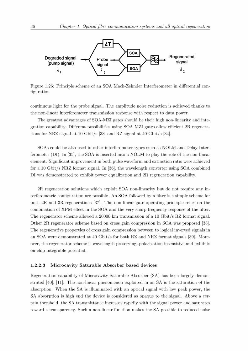
36 Chapter 1. Optical fibre communication systems and all-optical regeneration
SOA
SOA
∆T∆T
SOA
SOA
Degraded signal (pump signal)
Probe signal
Regenerated signal
1λ 2λ 2λ
SOA
SOA
∆T∆T∆T∆T
SOA
SOA
Degraded signal (pump signal)
Probe signal
Regenerated signal
1λ 2λ 2λ
Figure 1.26: Principle scheme of an SOA Mach-Zehnder Interferometer in differential con-figuration
continuous light for the probe signal. The amplitude noise reduction is achieved thanks to
the non-linear interferometer transmission response with respect to data power.
The greatest advantages of SOA-MZI gates should be their high non-linearity and inte-
gration capability. Different possibilities using SOA MZI gates allow efficient 2R regenera-
tions for NRZ signal at 10 Gbit/s [33] and RZ signal at 40 Gbit/s [34].
SOAs could be also used in other interferometer types such as NOLM and Delay Inter-
ferometer (DI). In [35], the SOA is inserted into a NOLM to play the role of the non-linear
element. Significant improvement in both pulse waveform and extinction ratio were achieved
for a 10 Gbit/s NRZ format signal. In [36], the wavelength converter using SOA combined
DI was demonstrated to exhibit power equalization and 2R regeneration capability.
2R regeneration solutions which exploit SOA non-linearity but do not require any in-
terferometric configuration are possible. An SOA followed by a filter is a simple scheme for
both 2R and 3R regenerations [37]. The non-linear gate operating principle relies on the
combination of XPM effect in the SOA and the very sharp frequency response of the filter.
The regenerator scheme allowed a 20000 km transmission of a 10 Gbit/s RZ format signal.
Other 2R regenerator scheme based on cross gain compression in SOA was proposed [38].
The regenerative properties of cross gain compression between to logical inverted signals in
an SOA were demonstrated at 40 Gbit/s for both RZ and NRZ format signals [39]. More-
over, the regenerator scheme is wavelength preserving, polarization insensitive and exhibits
on-chip integrable potential.
1.2.2.3 Microcavity Saturable Absorber based devices
Regeneration capability of Microcavity Saturable Absorber (SA) has been largely demon-
strated [40], [11]. The non-linear phenomenon exploited in an SA is the saturation of the
absorption. When the SA is illuminated with an optical signal with low peak power, the
SA absorption is high end the device is considered as opaque to the signal. Above a cer-
tain threshold, the SA transmittance increases rapidly with the signal power and saturates
toward a transparency. Such a non-linear function makes the SA possible to reduced noise
1.2. Signal regeneration and all-optical techniques 37
on the ‘0’ level, resulting in a higher contrast between ‘1’ and ‘0’ levels.
SAs do not suppress amplitude noise on the ‘1’ level, which makes it incomplete for a
regenerator. Various complementary devices have been proposed to be combined with an
SA for a complete 2R regenerator solution. One passive scheme is using optical filtering of
non-linear (soliton) pulses for ‘1’ noise suppression [41]. In the absence of chirp, a pulse
intensity increase or decrease corresponds to a spectral broadening or narrowing. An optical
filter will cause higher loss when intensity increases, and lower loss when intensity decreases.
Thus, the filter plays the role of a power control or power equalisation function. The 2R
regenerator scheme was demonstrated its efficiency at 40 Gbit/s in loop experiment [41].
It allows the transmission distance to be increased from 1300 km (without regenerator) to
7600 km (with regenerator) for a Q-factor of 13 dB. The first advantage of such regenerator
is that it is totally passive. Moreover, the solution is WDM compatible, it demonstrates
efficient 2R regeneration over a 13 nm wavelength range in the 1550 nm window [11].
Another solution is using SOA for ‘1’ level noise suppression. 2R regeneration at 10 Gbit/s
and WDM compatibility of the SOA-SA regenerator has been proven [10]. The regenerator
scheme is fully compatible with photonic integration and hence promises compact, low-cost
WDM 2R regeneration. Recently, novel saturable absorber which treats the high power
levels was proposed [42] and cascaded with the classical saturable absorber to constitute a
complete 2R regenerator scheme [43]. The dual-stage SA gate demonstrates its regenerative
properties at 40 Gbit/s. The two SAs are based on the same technology which promises
compact, low-cost, passive solutions for high speed 2R regeneration.
38 Chapter 1. Optical fibre communication systems and all-optical regeneration
1.3 Chapter summary
This first chapter presented the context of the thesis and introduced the basic notions of
optical fibre communication systems.
Our studies rely mainly on the point-to-point link type which is described in the first
section. The functional blocks used to emit and receive the transmitted optical signal as
well as the common modulation formats (RZ and NRZ) are described. Signal degrada-
tions occurring during the propagation are also developed to show the necessity of signal
regeneration, especially for long and ultralong haul transmissions. Fibre losses are the first
factor that leads to signal degradations and limits the transmission distance. When the bit
rate increases impairments caused by chromatic and polarisation mode dispersions become
rapidly critical factors. Non-linear effects and ASE accumulation are other sources of signal
degradations which could not be neglected. Finally, various criteria which are employed to
estimate the performance of a transmission are presented. Signal quality could be evaluated
qualitatively by observing electrical and/or optical eye diagrams. Quantitative criteria such
as the optical signal to noise ratio, quality factor and bit error rate are used to specify the
signal quality and estimate the system performance.
In the second section, regeneration processes (1R, 2R and 3R) and their principles are re-
viewed. It seems likely that all-optical regeneration solutions are more adequate for future
ultrahigh speed transmission systems rather than complex and ‘power hungry’ optoelec-
tronic solutions. A brief review of literature on 2R regeneration techniques is presented.
Fibre-based devices are advantageous for ultrahigh bit rate systems thanks to the ultrafast
response of the Kerr effect. Otherwise, semiconductor based devices could provide entirely
integrable and low cost solutions for 2R regeneration.
Chapter 2
Experimental characterisation of
different SOA structures
2.1 Semiconductor Optical Amplifiers for optical signal pro-
cessing
When monomode fibre imposed as the main information transporter in backbone network,
signal attenuation became the first factor that limited transmission distance. Optical am-
plifiers based on semiconductor or erbium-doped fibre were studied and developed with
the first goal of amplifying optical signal and thus improving the link budget. The Erbium
Doped Fibre Amplifier (EDFA) was invented in 1985 and led to a revolution in optical com-
munication systems in association with Wavelength Division Multiplexing (WDM). Only
in the 90s, optical amplifiers began being introduced in commercial transmission system,
firstly in terrestrial links. Nowadays, EDFA found their place in long haul links inside the
1550 nm window as linear amplifier.
First Semiconductor Optical Amplifiers (SOAs) were studied nearly at the same time
as the invention of semiconductor laser in the sixties. SOAs began attracting particular
interest for functional applications since the late of the eighties when InP/InGaAsP SOAs
designed to operate in the 1300 nm and 1550 nm windows appeared [25] and progress in anti-
reflection coating technology enabled fabrication of true travelling-wave amplifiers [44]. The
main applications of SOAs in current advanced optical communications could be divided
into 2 categories: booster amplification and non-linear signal processing applications.
There is an increasing interest in using SOA for booster amplification, particularly in
Metro and Access Networks. In this type of applications, a medium gain SOA is acceptable
as it is used to compensate for the loss of tens of km of SMF fibre. Broad optical band-
widths (up to 80 nm [45]) of SOA exhibit also advantage as an amplifier in transparent
network. Another type of SOA called Reflective SOA (R-SOA) finds its place in reflective
WDM-PON architectures, where the R-SOA is used as an amplifying modulator within a
‘colourless’ optical network unit.
40 Chapter 2. Experimental characterisation of different SOA structures
For many years, our laboratory has been working on optical functions for backbone
networks, such as all-optical regeneration and wavelength conversion. SOA with its poten-
tial in non-linear applications does not escape from our interest. The reason why EDFA,
not SOA, is chosen for long haul optical communications systems is also the reason why
SOA, not EDFA, is the active element of choice for optical signal processing: combination
of non-linearity and response time. Fibre amplifiers exhibit negligible non-linearities while
SOAs’ non-linearities can be severe. This fact makes that SOAs are much more suitable for
optical signal processing than fibre based amplifiers. The difference of response times be-
tween EDFA and SOA (from several milliseconds down to tens of picoseconds respectively)
is another reason. Amplification of an optical signal consumes carriers. When a modulated
light is injected into an amplifier, its gain is not maintained constant but passes transiently
by saturating state where the gain is depleted. If the amplifier does not provide the same
gain for all the data bits, patterning effects take place and quality of the optical data signal
is significantly degraded. To avoid distortion of the signal, the magnitude of gain satura-
tion must be sufficiently small, or the amplifier must be fast enough such that transient
gain changes do not affect the following bits. In the case of an EDFA, the gain recovery
time is typically in the millisecond region. For data rates of several Gigabit-per-second
regime (typical in point-to-point links of backbone networks), EDFA operates in the regime
of mean power saturation. The recovery time is much longer than the bit period (around
hundreds picoseconds) so that the amplifier effectively averages the power over very long
bit sequences. On the other hand, the order of magnitude of the carrier lifetimes in a SOA
is between some nanoseconds and some tens of picoseconds, which is much shorter than
those of an EDFA and are comparable to bit time slot for data rates of several Gbit/s.
Such dynamics of SOAs promise a potential for bit-by-bit signal processing.
The main goal of this chapter is to present experimental characterisation results of
different SOA structures. These SOAs are designed and fabricated by the Alcatel-Lucent
Thales III-V Lab in the frame work of the project FUTUR in order to perform functions
of optical regeneration and wavelength conversion at 40 Gbit/s and up to 160 Gbit/s.
As far as bulk based SOAs, two chips with a same waveguide length but with different
confinement factors are studied. As far as quantum-dot based SOAs are concerned, two
chips with different waveguide lengths are analysed. A quantum-dash SOA is also studied.
Our experimental studies concentrate on two mains aspects: gain non-linearity and gain
dynamics. All results are given in Sections 2.2 and 2.3. In the following of this section 2.1,
we remind briefly some basic descriptions of an SOA and some essential backgrounds about
gain saturation and SOA dynamics behaviour. These basic descriptions are principally
based on those of [46], [47], [48].
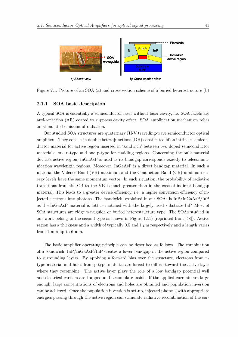
2.1. Semiconductor Optical Amplifiers for optical signal processing 41
SOA waveguide
a) Above view
N InP
SubstrateN-InP
P-InP
Electrode
InGaAsPactive region
b) Cross section view
SOA waveguide
a) Above view
SOA waveguide
SOA waveguide
SOA waveguide
a) Above view
N InP
SubstrateN-InP
P-InP
Electrode
InGaAsPactive region
b) Cross section view
N InP
SubstrateN-InP
P-InP
Electrode
InGaAsPactive region
N InP
SubstrateN-InP
P-InPN InP
SubstrateN-InP
P-InP
Electrode
InGaAsPactive region
b) Cross section view
Figure 2.1: Picture of an SOA (a) and cross-section scheme of a buried heterostructure (b)
2.1.1 SOA basic description
A typical SOA is essentially a semiconductor laser without laser cavity, i.e. SOA facets are
anti-reflection (AR) coated to suppress cavity effect. SOA amplification mechanism relies
on stimulated emission of radiation.
Our studied SOA structures are quaternary III-V travelling-wave semiconductor optical
amplifiers. They consist in double heterojunctions (DH) constituted of an intrinsic semicon-
ductor material for active region inserted in ‘sandwich’ between two doped semiconductor
materials: one n-type and one p-type for cladding regions. Concerning the bulk material
device’s active region, InGaAsP is used as its bandgap corresponds exactly to telecommu-
nication wavelength regions. Moreover, InGaAsP is a direct bandgap material. In such a
material the Valence Band (VB) maximum and the Conduction Band (CB) minimum en-
ergy levels have the same momentum vector. In such situation, the probability of radiative
transitions from the CB to the VB is much greater than in the case of indirect bandgap
material. This leads to a greater device efficiency, i.e. a higher conversion efficiency of in-
jected electrons into photons. The ‘sandwich’ exploited in our SOAs is InP/InGaAsP/InP
as the InGaAsP material is lattice matched with the largely used substrate InP. Most of
SOA structures are ridge waveguide or buried heterostructure type. The SOAs studied in
our work belong to the second type as shown in Figure (2.1) (reprinted from [48]). Active
region has a thickness and a width of typically 0.5 and 1 µm respectively and a length varies
from 1 mm up to 6 mm.
The basic amplifier operating principle can be described as follows. The combination
of a ‘sandwich’ InP/InGaAsP/InP creates a lower bandgap in the active region compared
to surrounding layers. By applying a forward bias over the structure, electrons from n-
type material and holes from p-type material are forced to diffuse toward the active layer
where they recombine. The active layer plays the role of a low bandgap potential well
and electrical carriers are trapped and accumulate inside. If the applied currents are large
enough, large concentrations of electrons and holes are obtained and population inversion
can be achieved. Once the population inversion is set-up, injected photons with appropriate
energies passing through the active region can stimulate radiative recombination of the car-
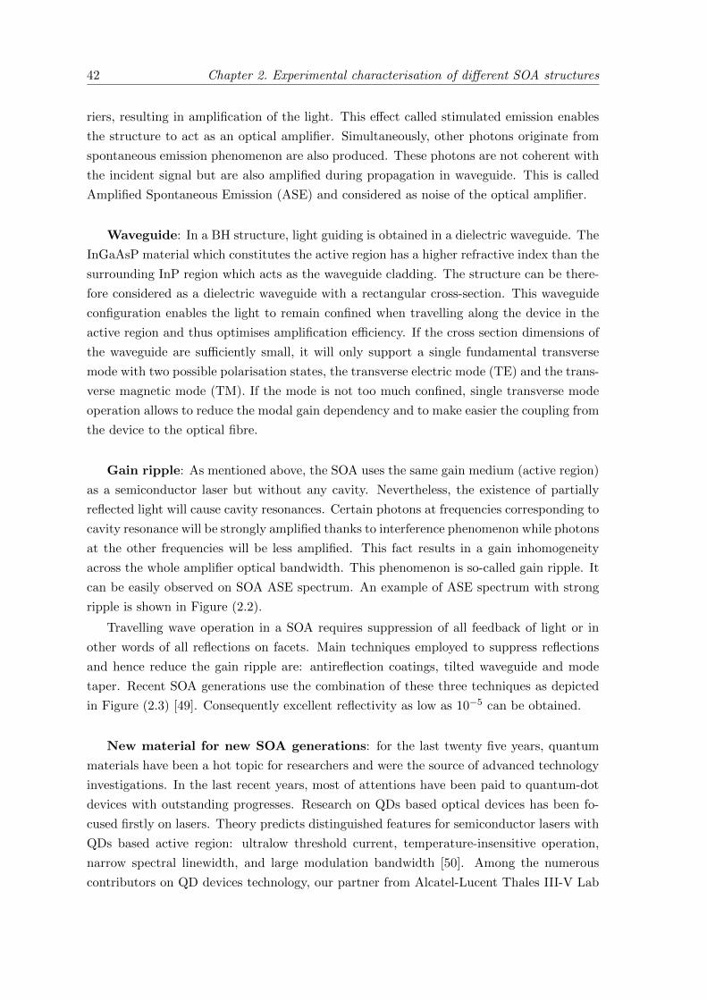
42 Chapter 2. Experimental characterisation of different SOA structures
riers, resulting in amplification of the light. This effect called stimulated emission enables
the structure to act as an optical amplifier. Simultaneously, other photons originate from
spontaneous emission phenomenon are also produced. These photons are not coherent with
the incident signal but are also amplified during propagation in waveguide. This is called
Amplified Spontaneous Emission (ASE) and considered as noise of the optical amplifier.
Waveguide: In a BH structure, light guiding is obtained in a dielectric waveguide. The
InGaAsP material which constitutes the active region has a higher refractive index than the
surrounding InP region which acts as the waveguide cladding. The structure can be there-
fore considered as a dielectric waveguide with a rectangular cross-section. This waveguide
configuration enables the light to remain confined when travelling along the device in the
active region and thus optimises amplification efficiency. If the cross section dimensions of
the waveguide are sufficiently small, it will only support a single fundamental transverse
mode with two possible polarisation states, the transverse electric mode (TE) and the trans-
verse magnetic mode (TM). If the mode is not too much confined, single transverse mode
operation allows to reduce the modal gain dependency and to make easier the coupling from
the device to the optical fibre.
Gain ripple: As mentioned above, the SOA uses the same gain medium (active region)
as a semiconductor laser but without any cavity. Nevertheless, the existence of partially
reflected light will cause cavity resonances. Certain photons at frequencies corresponding to
cavity resonance will be strongly amplified thanks to interference phenomenon while photons
at the other frequencies will be less amplified. This fact results in a gain inhomogeneity
across the whole amplifier optical bandwidth. This phenomenon is so-called gain ripple. It
can be easily observed on SOA ASE spectrum. An example of ASE spectrum with strong
ripple is shown in Figure (2.2).
Travelling wave operation in a SOA requires suppression of all feedback of light or in
other words of all reflections on facets. Main techniques employed to suppress reflections
and hence reduce the gain ripple are: antireflection coatings, tilted waveguide and mode
taper. Recent SOA generations use the combination of these three techniques as depicted
in Figure (2.3) [49]. Consequently excellent reflectivity as low as 10−5 can be obtained.
New material for new SOA generations: for the last twenty five years, quantum
materials have been a hot topic for researchers and were the source of advanced technology
investigations. In the last recent years, most of attentions have been paid to quantum-dot
devices with outstanding progresses. Research on QDs based optical devices has been fo-
cused firstly on lasers. Theory predicts distinguished features for semiconductor lasers with
QDs based active region: ultralow threshold current, temperature-insensitive operation,
narrow spectral linewidth, and large modulation bandwidth [50]. Among the numerous
contributors on QD devices technology, our partner from Alcatel-Lucent Thales III-V Lab
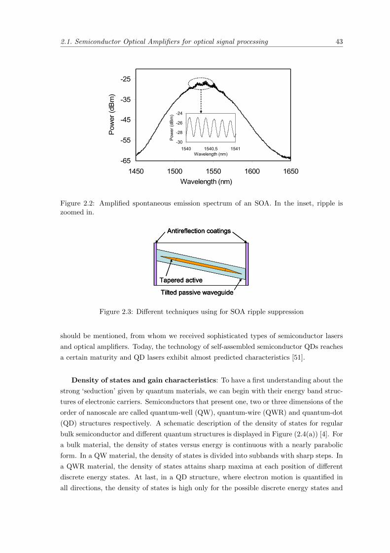
2.1. Semiconductor Optical Amplifiers for optical signal processing 43
-65
-55
-45
-35
-25
1450 1500 1550 1600 1650Wavelength (nm)
Pow
er (d
Bm
)
-30
-28
-26
-24
1540 1540,5 1541Wavelength (nm)
Pow
er (d
Bm
)
-65
-55
-45
-35
-25
1450 1500 1550 1600 1650Wavelength (nm)
Pow
er (d
Bm
)
-30
-28
-26
-24
1540 1540,5 1541Wavelength (nm)
Pow
er (d
Bm
)
Figure 2.2: Amplified spontaneous emission spectrum of an SOA. In the inset, ripple iszoomed in.
Antireflection coatings
Tilted passive waveguide
Tapered active
Antireflection coatingsAntireflection coatings
Tilted passive waveguideTilted passive waveguide
Tapered activeTapered active
Figure 2.3: Different techniques using for SOA ripple suppression
should be mentioned, from whom we received sophisticated types of semiconductor lasers
and optical amplifiers. Today, the technology of self-assembled semiconductor QDs reaches
a certain maturity and QD lasers exhibit almost predicted characteristics [51].
Density of states and gain characteristics: To have a first understanding about the
strong ‘seduction’ given by quantum materials, we can begin with their energy band struc-
tures of electronic carriers. Semiconductors that present one, two or three dimensions of the
order of nanoscale are called quantum-well (QW), quantum-wire (QWR) and quantum-dot
(QD) structures respectively. A schematic description of the density of states for regular
bulk semiconductor and different quantum structures is displayed in Figure (2.4(a)) [4]. For
a bulk material, the density of states versus energy is continuous with a nearly parabolic
form. In a QW material, the density of states is divided into subbands with sharp steps. In
a QWR material, the density of states attains sharp maxima at each position of different
discrete energy states. At last, in a QD structure, where electron motion is quantified in
all directions, the density of states is high only for the possible discrete energy states and
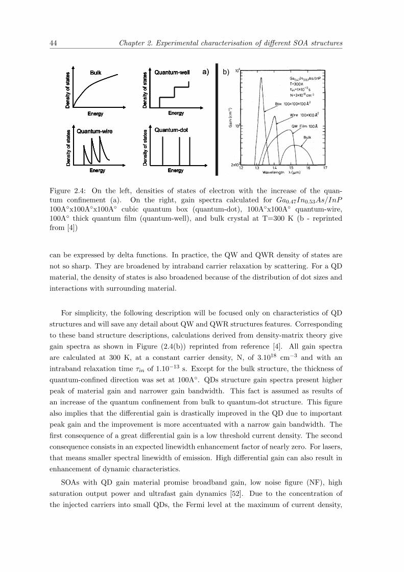
44 Chapter 2. Experimental characterisation of different SOA structures
Energy
Den
sity
of s
tate
s Bulk
Energy
Den
sity
of s
tate
s Quantum-well
Energy
Den
sity
of s
tate
s Quantum-wire
Energy
Den
sity
of s
tate
s Quantum-dot
a) b)
Energy
Den
sity
of s
tate
s Bulk
Energy
Den
sity
of s
tate
s Quantum-well
Energy
Den
sity
of s
tate
s Quantum-wire
Energy
Den
sity
of s
tate
s Quantum-dot
Energy
Den
sity
of s
tate
s Bulk
Energy
Den
sity
of s
tate
s Quantum-well
Energy
Den
sity
of s
tate
s Quantum-wire
Energy
Den
sity
of s
tate
s Quantum-dot
Energy
Den
sity
of s
tate
s Bulk
Energy
Den
sity
of s
tate
s Bulk
Energy
Den
sity
of s
tate
s Quantum-well
Energy
Den
sity
of s
tate
s Quantum-well
Energy
Den
sity
of s
tate
s Quantum-wire
Energy
Den
sity
of s
tate
s Quantum-wire
Energy
Den
sity
of s
tate
s Quantum-dot
Energy
Den
sity
of s
tate
s Quantum-dot
a) b)
Figure 2.4: On the left, densities of states of electron with the increase of the quan-tum confinement (a). On the right, gain spectra calculated for Ga0.47In0.53As/InP100A◦x100A◦x100A◦ cubic quantum box (quantum-dot), 100A◦x100A◦ quantum-wire,100A◦ thick quantum film (quantum-well), and bulk crystal at T=300 K (b - reprintedfrom [4])
can be expressed by delta functions. In practice, the QW and QWR density of states are
not so sharp. They are broadened by intraband carrier relaxation by scattering. For a QD
material, the density of states is also broadened because of the distribution of dot sizes and
interactions with surrounding material.
For simplicity, the following description will be focused only on characteristics of QD
structures and will save any detail about QW and QWR structures features. Corresponding
to these band structure descriptions, calculations derived from density-matrix theory give
gain spectra as shown in Figure (2.4(b)) reprinted from reference [4]. All gain spectra
are calculated at 300 K, at a constant carrier density, N, of 3.1018 cm−3 and with an
intraband relaxation time τin of 1.10−13 s. Except for the bulk structure, the thickness of
quantum-confined direction was set at 100A◦. QDs structure gain spectra present higher
peak of material gain and narrower gain bandwidth. This fact is assumed as results of
an increase of the quantum confinement from bulk to quantum-dot structure. This figure
also implies that the differential gain is drastically improved in the QD due to important
peak gain and the improvement is more accentuated with a narrow gain bandwidth. The
first consequence of a great differential gain is a low threshold current density. The second
consequence consists in an expected linewidth enhancement factor of nearly zero. For lasers,
that means smaller spectral linewidth of emission. High differential gain can also result in
enhancement of dynamic characteristics.
SOAs with QD gain material promise broadband gain, low noise figure (NF), high
saturation output power and ultrafast gain dynamics [52]. Due to the concentration of
the injected carriers into small QDs, the Fermi level at the maximum of current density,
2.1. Semiconductor Optical Amplifiers for optical signal processing 45
which is limited by the thermal effect, is significantly increased. Direct consequence of this
phenomenon is the expansion of gain wavelength range [46], [47]. High saturation output
power and low NF result from a combination of a highly filled carrier reservoir (assigned
to wetting-layer) and a small overlap between the optical field and the QDs [53]. A general
description of ultrafast gain dynamics of QD SOA will be presented later in Section 2.1.3.
QD SOA with record widest bandwidth of 120 nm and high output saturation power higher
than 19 dBm was demonstrated [52], a low NF close to 5 dB was achieved [52], [51]. Ultrafast
dynamics of QD SOA also make effective all-optical signal processing without important
patterning effects possible at ultrahigh bit rates of 40 Gbit/s and 160 Gbit/s [54], [55].
2.1.2 Gain saturation
If a large enough forward current is applied to a SOA, a population inversion in active region
can be achieved. The SOA presents a gain for optical signals satisfying the Bernard and
Duraffourg condition (Equation (2-1)), i.e. if the photon energies are larger than the energy
bandgap between the conduction and the valence bands and smaller than the gap between
their Fermi levels, which are representative of how the bands are filled with carriers.
Eg < E < ∆EF (2-1)
E is the photon energy
Eg is the bandgap
∆EF is the distance between the Fermi levels of the conduction and valance bands
Amplification of light consumes carriers as it relies on electron-hole recombinations by
stimulated emission. The amplification of an optical signal therefore decreases the density
of carriers. If the optical signal power is large enough such that consequent stimulated
emission consumes more carriers than that could be supplied by injected bias current, then
the presence of optical signal leads to a drop of total carrier density or in other words a de-
crease of overall-optical gain. The phenomenon is called gain saturation. When the injected
light is a modulated signal, i.e. a pulse stream, the gain saturation varies in time and the
phenomenon is rather called gain compression or dynamic gain saturation. This dynamic
gain saturation of an SOA will be discussed in details in Section 2.1.3. In this section, we
consider the gain saturation by an injected continuous optical signal. In this case the SOA
gain is in a steady state, and gain saturation analysis provides primary information about
the non-linearity provided by SOAs.
There are a lot of SOA models with varying complexity [56], [57], [15], [58]. To describe
the gain saturation in a steady state, we use the model presented by [56] which appears as
one of the simplest models while providing a clear understanding about gain saturation.
The model considers an optical signal propagating along a travelling-wave SOA. It
is assumed that the width w and the thickness d of the active region are small enough
46 Chapter 2. Experimental characterisation of different SOA structures
compared to the scattering length to consider the carrier density as nearly uniform along
the transverse dimensions. In practice, our SOA are in order of 1 µm of width and 0.5 µm
of thickness, the assumption is then verified. By averaging over the active region, carrier
density evolution is given by the differential Equation (2-2):
∂M
∂t=
I
qV− M
τs− g (M)
hω0|A|2 (2-2)
M is the carrier density
I is the injected current
V is the volume of the active region
τs is the carrier relaxation time
h is the reduced Planck constant
ω0 is the signal pulsation in vacuum
A (z, t) is the slowly-varying envelope associated with the optical field
t is the time
z is the spatial variable along the amplifier length
g (M) is the intrinsic gain of the SOA
On the right side of Equation (2-2), the first term represents the carrier density supplied
by external injected current. The second one represents the loss of carrier density due to
interband relaxation and the last one represents the drop of carrier density due to stimulated
emission. In a static regime, the carrier density M is a constant; the left side of Equation (2-
2) cancels. The carrier density value satisfies Equation (2-3):
I
qV− M
τs− g (M)
hω0|A|2 = 0 (2-3)
The intrinsic gain is a function of carrier density and defined by Equation (2-4):
g (M) = Γa (M −M0) (2-4)
Γ is the confinement factor
a is the material gain coefficient
M0 is the carrier density required for transparency
If we define the saturation energy Esat and the small-signal intrinsic gain g0 by (2-5)
and (2-6):
Esat =hω0σ
a(2-5)
g0 = ΓaM0
(I
I0− 1
)(2-6)
with the mode cross section:
σ =wd
Γ(2-7)
2.1. Semiconductor Optical Amplifiers for optical signal processing 47
the current at the transparency
I0 =qVM0
τs(2-8)
and the power of the optical signal:
P = |A|2 (2-9)
then, Equation (2-3) can be written as Equation (2-10):
g0 − gτs
− gP
Esat= 0 (2-10)
Equation (2-10) can be resolved directly to obtain Equation (2-11) relating the intrinsic
gain g as a function of the signal input power.
g (z) =g0
1 + P (z)Psat
(2-11)
with the saturation power defined as:
Psat =Esatτs
(2-12)
Equation (2-12) demonstrates clearly the phenomenon of gain saturation mentioned
above. A large enough input power will lead to a decrease of the intrinsic gain and con-
sequently of the overall amplifier gain. Psat is a parameter characterising the SOA gain
saturation. It represents the input signal power value such that the intrinsic gain drops to
a half of its maximal value, i.e g0/2.
In practice, it is not possible to measure the intrinsic gain g. On the contrary, we can
measure the signal power at the SOA input and output to deduce the amplifier gain, i.e
the gain accumulated by the signal along the amplifier length. We remind also that the
considered optical signal is continuous, then if we consider in the reference frame moving
at the group velocity of light, the signal power P will be a function of only z and not be a
function of time t any more. By neglecting internal loss of the amplifier, equation governing
the evolution of the optical power is given by Equation (2-13):
dP
dz= gP (2-13)
By integrating Equation (2-13) over the amplifier length, we obtain Equation (2-14):
P (L) = P (0) exp
L∫0
g (z) dz
(2-14)
Amplifier gain G accumulated by the incident signal by passing through the SOA is
defined by Equation (2-15):
G =P (L)
P (0)= exp
L∫0
g (z) dz
(2-15)
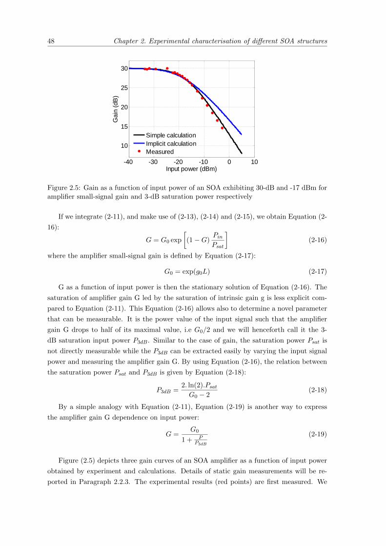
48 Chapter 2. Experimental characterisation of different SOA structures
-40 -30 -20 -10 0 10
10
15
20
25
30
Input power (dBm)
Gai
n (d
B)
Simple calculationImplicit calculationMeasured
Figure 2.5: Gain as a function of input power of an SOA exhibiting 30-dB and -17 dBm foramplifier small-signal gain and 3-dB saturation power respectively
If we integrate (2-11), and make use of (2-13), (2-14) and (2-15), we obtain Equation (2-
16):
G = G0 exp
[(1−G)
PinPsat
](2-16)
where the amplifier small-signal gain is defined by Equation (2-17):
G0 = exp(g0L) (2-17)
G as a function of input power is then the stationary solution of Equation (2-16). The
saturation of amplifier gain G led by the saturation of intrinsic gain g is less explicit com-
pared to Equation (2-11). This Equation (2-16) allows also to determine a novel parameter
that can be measurable. It is the power value of the input signal such that the amplifier
gain G drops to half of its maximal value, i.e G0/2 and we will henceforth call it the 3-
dB saturation input power P3dB. Similar to the case of gain, the saturation power Psat is
not directly measurable while the P3dB can be extracted easily by varying the input signal
power and measuring the amplifier gain G. By using Equation (2-16), the relation between
the saturation power Psat and P3dB is given by Equation (2-18):
P3dB =2. ln(2).PsatG0 − 2
(2-18)
By a simple analogy with Equation (2-11), Equation (2-19) is another way to express
the amplifier gain G dependence on input power:
G =G0
1 + PP3dB
(2-19)
Figure (2.5) depicts three gain curves of an SOA amplifier as a function of input power
obtained by experiment and calculations. Details of static gain measurements will be re-
ported in Paragraph 2.2.3. The experimental results (red points) are first measured. We
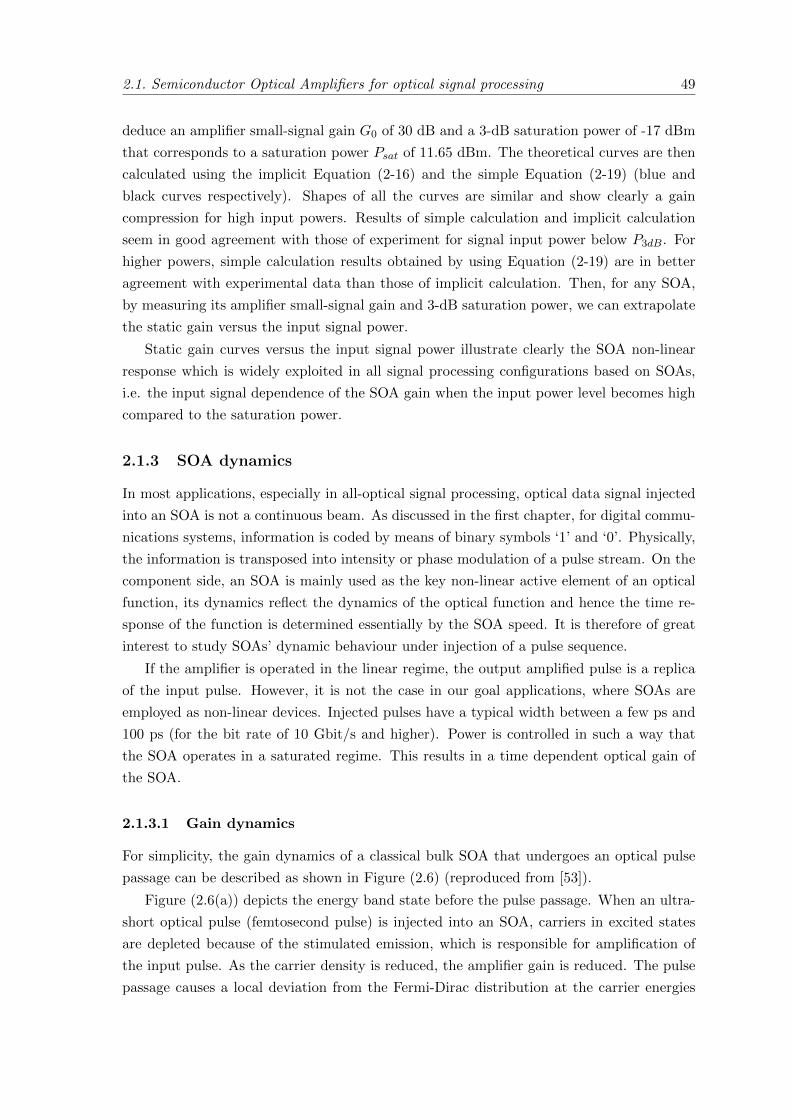
2.1. Semiconductor Optical Amplifiers for optical signal processing 49
deduce an amplifier small-signal gain G0 of 30 dB and a 3-dB saturation power of -17 dBm
that corresponds to a saturation power Psat of 11.65 dBm. The theoretical curves are then
calculated using the implicit Equation (2-16) and the simple Equation (2-19) (blue and
black curves respectively). Shapes of all the curves are similar and show clearly a gain
compression for high input powers. Results of simple calculation and implicit calculation
seem in good agreement with those of experiment for signal input power below P3dB. For
higher powers, simple calculation results obtained by using Equation (2-19) are in better
agreement with experimental data than those of implicit calculation. Then, for any SOA,
by measuring its amplifier small-signal gain and 3-dB saturation power, we can extrapolate
the static gain versus the input signal power.
Static gain curves versus the input signal power illustrate clearly the SOA non-linear
response which is widely exploited in all signal processing configurations based on SOAs,
i.e. the input signal dependence of the SOA gain when the input power level becomes high
compared to the saturation power.
2.1.3 SOA dynamics
In most applications, especially in all-optical signal processing, optical data signal injected
into an SOA is not a continuous beam. As discussed in the first chapter, for digital commu-
nications systems, information is coded by means of binary symbols ‘1’ and ‘0’. Physically,
the information is transposed into intensity or phase modulation of a pulse stream. On the
component side, an SOA is mainly used as the key non-linear active element of an optical
function, its dynamics reflect the dynamics of the optical function and hence the time re-
sponse of the function is determined essentially by the SOA speed. It is therefore of great
interest to study SOAs’ dynamic behaviour under injection of a pulse sequence.
If the amplifier is operated in the linear regime, the output amplified pulse is a replica
of the input pulse. However, it is not the case in our goal applications, where SOAs are
employed as non-linear devices. Injected pulses have a typical width between a few ps and
100 ps (for the bit rate of 10 Gbit/s and higher). Power is controlled in such a way that
the SOA operates in a saturated regime. This results in a time dependent optical gain of
the SOA.
2.1.3.1 Gain dynamics
For simplicity, the gain dynamics of a classical bulk SOA that undergoes an optical pulse
passage can be described as shown in Figure (2.6) (reproduced from [53]).
Figure (2.6(a)) depicts the energy band state before the pulse passage. When an ultra-
short optical pulse (femtosecond pulse) is injected into an SOA, carriers in excited states
are depleted because of the stimulated emission, which is responsible for amplification of
the input pulse. As the carrier density is reduced, the amplifier gain is reduced. The pulse
passage causes a local deviation from the Fermi-Dirac distribution at the carrier energies
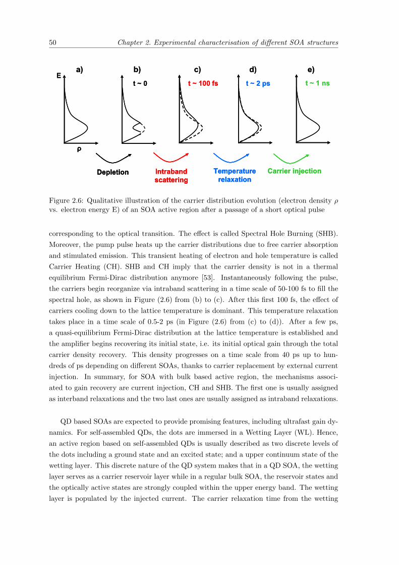
50 Chapter 2. Experimental characterisation of different SOA structures
E
ρ
t ~ 100 fst ~ 0 t ~ 2 ps t ~ 1 ns
Depletion Intrabandscattering
Temperaturerelaxation
Carrier injection
a) b) c) d) e)E
ρ
t ~ 100 fst ~ 0 t ~ 2 ps t ~ 1 ns
DepletionDepletion IntrabandscatteringIntrabandscattering
Temperaturerelaxation
Temperaturerelaxation
Carrier injectionCarrier injection
a) b) c) d) e)
Figure 2.6: Qualitative illustration of the carrier distribution evolution (electron density ρvs. electron energy E) of an SOA active region after a passage of a short optical pulse
corresponding to the optical transition. The effect is called Spectral Hole Burning (SHB).
Moreover, the pump pulse heats up the carrier distributions due to free carrier absorption
and stimulated emission. This transient heating of electron and hole temperature is called
Carrier Heating (CH). SHB and CH imply that the carrier density is not in a thermal
equilibrium Fermi-Dirac distribution anymore [53]. Instantaneously following the pulse,
the carriers begin reorganize via intraband scattering in a time scale of 50-100 fs to fill the
spectral hole, as shown in Figure (2.6) from (b) to (c). After this first 100 fs, the effect of
carriers cooling down to the lattice temperature is dominant. This temperature relaxation
takes place in a time scale of 0.5-2 ps (in Figure (2.6) from (c) to (d)). After a few ps,
a quasi-equilibrium Fermi-Dirac distribution at the lattice temperature is established and
the amplifier begins recovering its initial state, i.e. its initial optical gain through the total
carrier density recovery. This density progresses on a time scale from 40 ps up to hun-
dreds of ps depending on different SOAs, thanks to carrier replacement by external current
injection. In summary, for SOA with bulk based active region, the mechanisms associ-
ated to gain recovery are current injection, CH and SHB. The first one is usually assigned
as interband relaxations and the two last ones are usually assigned as intraband relaxations.
QD based SOAs are expected to provide promising features, including ultrafast gain dy-
namics. For self-assembled QDs, the dots are immersed in a Wetting Layer (WL). Hence,
an active region based on self-assembled QDs is usually described as two discrete levels of
the dots including a ground state and an excited state; and a upper continuum state of the
wetting layer. This discrete nature of the QD system makes that in a QD SOA, the wetting
layer serves as a carrier reservoir layer while in a regular bulk SOA, the reservoir states and
the optically active states are strongly coupled within the upper energy band. The wetting
layer is populated by the injected current. The carrier relaxation time from the wetting
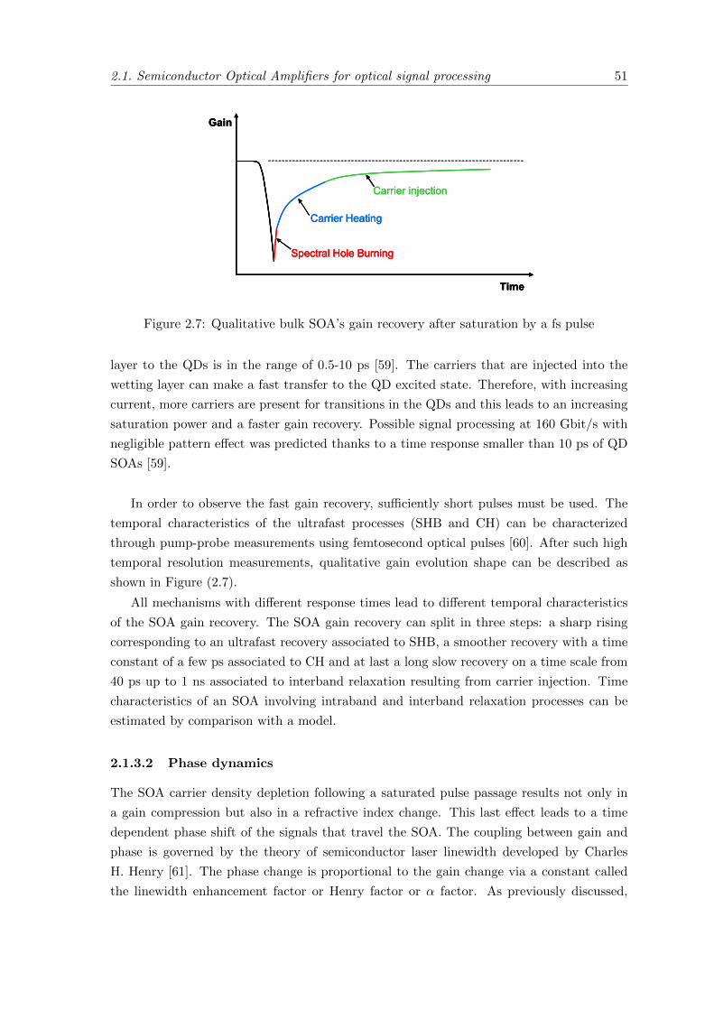
2.1. Semiconductor Optical Amplifiers for optical signal processing 51
Gain
Time
Spectral Hole Burning
Carrier Heating
Carrier injection
Gain
Time
Gain
Time
Spectral Hole BurningSpectral Hole Burning
Carrier HeatingCarrier Heating
Carrier injectionCarrier injection
Figure 2.7: Qualitative bulk SOA’s gain recovery after saturation by a fs pulse
layer to the QDs is in the range of 0.5-10 ps [59]. The carriers that are injected into the
wetting layer can make a fast transfer to the QD excited state. Therefore, with increasing
current, more carriers are present for transitions in the QDs and this leads to an increasing
saturation power and a faster gain recovery. Possible signal processing at 160 Gbit/s with
negligible pattern effect was predicted thanks to a time response smaller than 10 ps of QD
SOAs [59].
In order to observe the fast gain recovery, sufficiently short pulses must be used. The
temporal characteristics of the ultrafast processes (SHB and CH) can be characterized
through pump-probe measurements using femtosecond optical pulses [60]. After such high
temporal resolution measurements, qualitative gain evolution shape can be described as
shown in Figure (2.7).
All mechanisms with different response times lead to different temporal characteristics
of the SOA gain recovery. The SOA gain recovery can split in three steps: a sharp rising
corresponding to an ultrafast recovery associated to SHB, a smoother recovery with a time
constant of a few ps associated to CH and at last a long slow recovery on a time scale from
40 ps up to 1 ns associated to interband relaxation resulting from carrier injection. Time
characteristics of an SOA involving intraband and interband relaxation processes can be
estimated by comparison with a model.
2.1.3.2 Phase dynamics
The SOA carrier density depletion following a saturated pulse passage results not only in
a gain compression but also in a refractive index change. This last effect leads to a time
dependent phase shift of the signals that travel the SOA. The coupling between gain and
phase is governed by the theory of semiconductor laser linewidth developed by Charles
H. Henry [61]. The phase change is proportional to the gain change via a constant called
the linewidth enhancement factor or Henry factor or α factor. As previously discussed,
52 Chapter 2. Experimental characterisation of different SOA structures
650 700 750 800 850 900 950 10000.2
0.4
0.6
0.8
1
Time (ps)
Nor
mal
ised
gai
n
650 700 750 800 850 900 950 1000
0
0.5
1
Time (ps)
Nor
mal
ised
pha
se
Figure 2.8: SOA dynamics: Gain recovery exhibits an ultrafast component and a slowcomponent (upper trace) while phase recovery exhibits only a slow component (lower trace)
the gain is recovered through three different mechanisms: SHB, CH and carrier interband
relaxation. Separate measurements of gain and phase recovery have shown different α-
factor values associated to the three processes [62]. The α value has been estimated to
be 0 for the SHB process, 1 for the CH process and 5-8 for the normal carrier band to
band relaxation [63]. The small α factors for fast processes suggest that the phase recovery
is slower than the gain recovery. This last prediction has been demonstrated by some
experiments [64], [62], [65]. Trace examples of gain and of phase recoveries are illustrated
in Figure (2.8) obtained by simulation using the model that will be developed in Chapter
3. The SOA is supposed to be saturated by a 2 ps pulse stream.
The gain recovery trace displays two steps with two different temporal characteristics.
The first step can be characterised by a time constant in order of few ps. This first gain
recovery part is dominated by intraband relaxations (SHB and CH). The SHB effect is
masked by the pulse length which is much longer than the SHB process and can not be
observed because of the long pulse duration compared to the time scale of SHB effect (2 ps
vs. 100 fs). However, as the pulse length is a little bit longer than the CH dynamics, this
last contribution can be seen in the first part of the gain recovery curve. The second step
exhibits a temporal characteristic in order of 100 ps that is the signature of carrier interband
relaxation. On the other side, phase recovery rather seems to be characterised by only one
time constant in the same order of 100 ps. This last observation illustrates the fact that the
coupling between phase and gain changes caused by total carrier density reduction is much
stronger than the coupling phase gain associated to the ultrafast intraband processes. This
phase-gain dynamics difference should be taken into account carefully in signal processing

2.1. Semiconductor Optical Amplifiers for optical signal processing 53
configurations that exploit simultaneously cross-gain and cross-phase modulations in SOAs.
54 Chapter 2. Experimental characterisation of different SOA structures
2.2 Static characteristics
2.2.1 Description of the investigated SOAs
As previously mentioned in Section 2.1, all the SOAs studied in this thesis have been
supplied by the Alcatel-Lucent Thales III-V Lab in the framework of the national project
FUTUR. SOAs with different structures and materials are designed and fabricated in order
to perform functions of optical regeneration and wavelength conversion at 40 Gbit/s up to
160 Gbit/s. The main factor that limits SOA based signal processing function performances
for bit rates superior to 10 Gbit/s is the SOA dynamics that is not so fast. It is shown
that the effective carrier lifetime which is related to the SOA time response, can be reduced
by increasing the waveguide confinement factor [66]. Ultrafast gain dynamics are also
expected from new quantum structures [50], [53]. In such vision, we investigated various
SOA structures described in Table (2.1). The SOA structure information is given by our
SOA supplier.
Chip Material Confinement Waveguide Maximalnumber length (mm) bias current (mA)
1 Bulk 20 % 1 300
2 Bulk 80 % 1 400
3 Quantum-dot 6 QDot layers 2 500
4 Quantum-dash 6 QDash layers 2 300
5 Quantum-dot 3 QDot layers 5 800
Table 2.1: Characterised SOAs
All SOAs are buried heterostructures except for the sample n◦5 which is a ridge waveg-
uide. For standard SOAs based on bulk material, two chips with the same waveguide
length but different confinement factors are studied. The material of active region is In-
GaAsP which is grown on an InP substrate. As far as quantum material based SOAs are
concerned, two quantum-dot SOAs with different waveguide length are analysed, as well
as a quantum-dash (elongated dot) SOA [51]. Supplied SOAs are chips on submount. The
last three SOAs are constituted of InAs/InP QD material allowing operation in the telecom
wavelength window [1.4 µm-1.6 µm] [51]. For all characterisations, unless mentioned, SOAs
are controlled at typical room temperature, i.e. 25◦C.
In almost characterisation experiments, laser signal that is injected into SOAs is guided
by an optical fibre and signal emitted by SOAs has to be transported also by an optical
fibre to the analysis instrument. Coupling between SOA chips and fibres is realised by two
injection benches using micro-lensed fibres and lenses for coupling.
Micro-lensed fibre coupling bed
Micro-lensed fibre coupling bed is shown in Figure (2.9). It consists mainly of a chip
support including temperature control and translation in y and z directions, a bias current
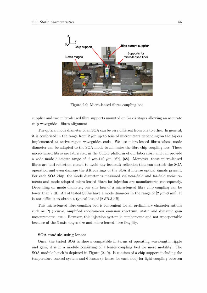
2.2. Static characteristics 55
3-axis stagesSupports for
micro-lensed fiber
Bias current supplierChip support
xy
z
3-axis stagesSupports for
micro-lensed fiber
Bias current supplierChip support
3-axis stages3-axis stagesSupports for
micro-lensed fiber
Bias current supplier
Supports for micro-lensed fiber
Supports for micro-lensed fiber
Bias current supplierBias current supplierChip supportChip support
xy
z
xy
z
Figure 2.9: Micro-lensed fibres coupling bed
supplier and two micro-lensed fibre supports mounted on 3-axis stages allowing an accurate
chip waveguide - fibres alignment.
The optical mode diameter of an SOA can be very different from one to other. In general,
it is comprised in the range from 2 µm up to tens of micrometers depending on the tapers
implemented at active region waveguides ends. We use micro-lensed fibres whose mode
diameter can be adapted to the SOA mode to minimise the fibre-chip coupling loss. These
micro-lensed fibres are fabricated in the CCLO platform of our laboratory and can provide
a wide mode diameter range of [2 µm-140 µm] [67], [68]. Moreover, these micro-lensed
fibres are anti-reflection coated to avoid any feedback reflection that can disturb the SOA
operation and even damage the AR coatings of the SOA if intense optical signals present.
For each SOA chip, the mode diameter is measured via near-field and far-field measure-
ments and mode-adapted micro-lensed fibres for injection are manufactured consequently.
Depending on mode diameter, one side loss of a micro-lensed fibre chip coupling can be
lower than 2 dB. All of tested SOAs have a mode diameter in the range of [2 µm-8 µm]. It
is not difficult to obtain a typical loss of [2 dB-3 dB].
This micro-lensed fibre coupling bed is convenient for all preliminary characterisations
such as P(I) curve, amplified spontaneous emission spectrum, static and dynamic gain
measurements, etc... However, this injection system is cumbersome and not transportable
because of the 3-axis stages size and micro-lensed fibre fragility.
SOA module using lenses
Once, the tested SOA is shown compatible in terms of operating wavelength, ripple
and gain, it is in a module consisting of a lenses coupling bed for more mobility. The
SOA module bench is depicted in Figure (2.10). It consists of a chip support including the
temperature control system and 6 lenses (3 lenses for each side) for light coupling between
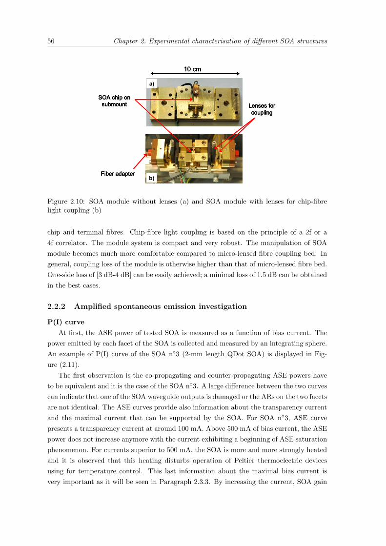
56 Chapter 2. Experimental characterisation of different SOA structures
SOA chip on submount Lenses for
coupling
Fiber adapter
a)
b)
10 cm
SOA chip on submount Lenses for
coupling
Fiber adapter
a)
b)
SOA chip on submount
SOA chip on submount Lenses for
couplingLenses for coupling
Fiber adapterFiber adapter
a)
b)
10 cm10 cm
Figure 2.10: SOA module without lenses (a) and SOA module with lenses for chip-fibrelight coupling (b)
chip and terminal fibres. Chip-fibre light coupling is based on the principle of a 2f or a
4f correlator. The module system is compact and very robust. The manipulation of SOA
module becomes much more comfortable compared to micro-lensed fibre coupling bed. In
general, coupling loss of the module is otherwise higher than that of micro-lensed fibre bed.
One-side loss of [3 dB-4 dB] can be easily achieved; a minimal loss of 1.5 dB can be obtained
in the best cases.
2.2.2 Amplified spontaneous emission investigation
P(I) curve
At first, the ASE power of tested SOA is measured as a function of bias current. The
power emitted by each facet of the SOA is collected and measured by an integrating sphere.
An example of P(I) curve of the SOA n◦3 (2-mm length QDot SOA) is displayed in Fig-
ure (2.11).
The first observation is the co-propagating and counter-propagating ASE powers have
to be equivalent and it is the case of the SOA n◦3. A large difference between the two curves
can indicate that one of the SOA waveguide outputs is damaged or the ARs on the two facets
are not identical. The ASE curves provide also information about the transparency current
and the maximal current that can be supported by the SOA. For SOA n◦3, ASE curve
presents a transparency current at around 100 mA. Above 500 mA of bias current, the ASE
power does not increase anymore with the current exhibiting a beginning of ASE saturation
phenomenon. For currents superior to 500 mA, the SOA is more and more strongly heated
and it is observed that this heating disturbs operation of Peltier thermoelectric devices
using for temperature control. This last information about the maximal bias current is
very important as it will be seen in Paragraph 2.3.3. By increasing the current, SOA gain
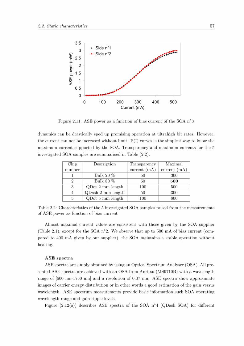
2.2. Static characteristics 57
0
0,5
1
1,5
2
2,5
3
3,5
0 100 200 300 400 500Current (mA)
AS
E p
ower
(mW
)
Side n°1Side n°2
Figure 2.11: ASE power as a function of bias current of the SOA n◦3
dynamics can be drastically sped up promising operation at ultrahigh bit rates. However,
the current can not be increased without limit. P(I) curves is the simplest way to know the
maximum current supported by the SOA. Transparency and maximum currents for the 5
investigated SOA samples are summarised in Table (2.2).
Chip Description Transparency Maximalnumber current (mA) current (mA)
1 Bulk 20 % 50 300
2 Bulk 80 % 50 500
3 QDot 2 mm length 100 500
4 QDash 2 mm length 50 300
5 QDot 5 mm length 100 800
Table 2.2: Characteristics of the 5 investigated SOA samples raised from the measurementsof ASE power as function of bias current
Almost maximal current values are consistent with those given by the SOA supplier
(Table 2.1), except for the SOA n◦2. We observe that up to 500 mA of bias current (com-
pared to 400 mA given by our supplier), the SOA maintains a stable operation without
heating.
ASE spectra
ASE spectra are simply obtained by using an Optical Spectrum Analyser (OSA). All pre-
sented ASE spectra are achieved with an OSA from Anritsu (MS9710B) with a wavelength
range of [600 nm-1750 nm] and a resolution of 0.07 nm. ASE spectra show approximate
images of carrier energy distribution or in other words a good estimation of the gain versus
wavelength. ASE spectrum measurements provide basic information such SOA operating
wavelength range and gain ripple levels.
Figure (2.12(a)) describes ASE spectra of the SOA n◦4 (QDash SOA) for different
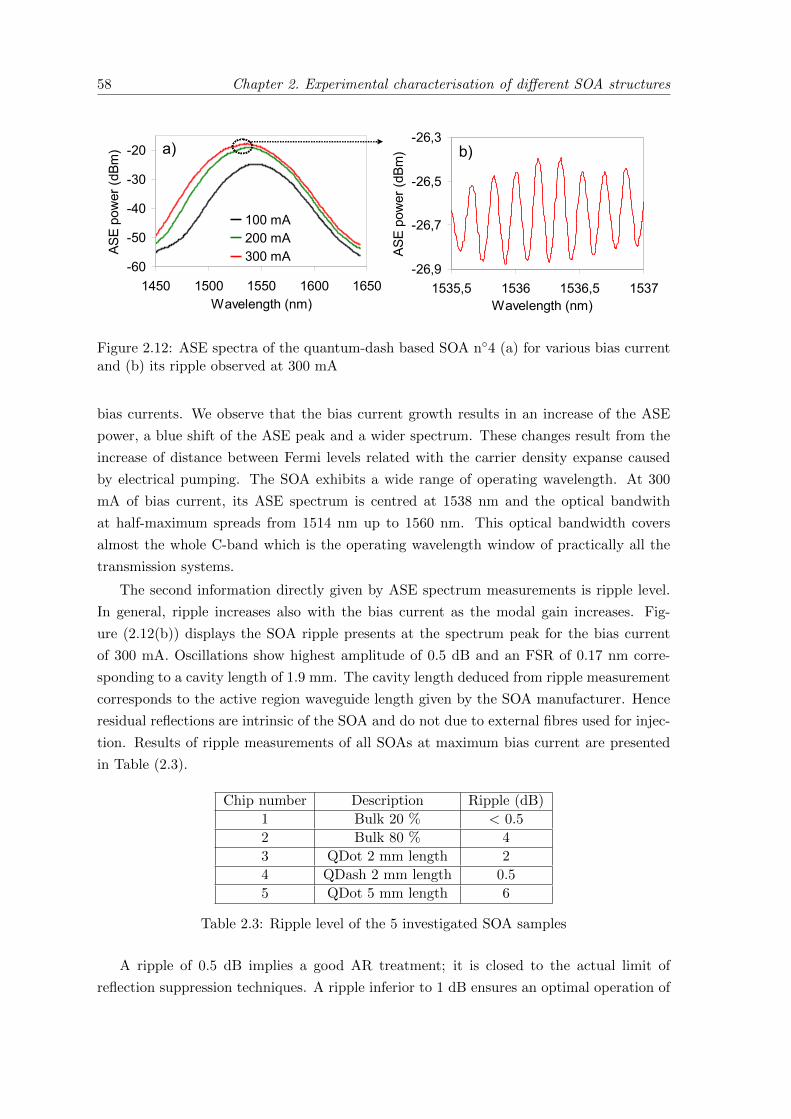
58 Chapter 2. Experimental characterisation of different SOA structures
-60
-50
-40
-30
-20
1450 1500 1550 1600 1650Wavelength (nm)
ASE
pow
er (d
Bm)
100 mA200 mA300 mA
-26,9
-26,7
-26,5
-26,3
1535,5 1536 1536,5 1537Wavelength (nm)
ASE
pow
er (d
Bm)a) b)
-60
-50
-40
-30
-20
1450 1500 1550 1600 1650Wavelength (nm)
ASE
pow
er (d
Bm)
100 mA200 mA300 mA
-26,9
-26,7
-26,5
-26,3
1535,5 1536 1536,5 1537Wavelength (nm)
ASE
pow
er (d
Bm)a) b)
Figure 2.12: ASE spectra of the quantum-dash based SOA n◦4 (a) for various bias currentand (b) its ripple observed at 300 mA
bias currents. We observe that the bias current growth results in an increase of the ASE
power, a blue shift of the ASE peak and a wider spectrum. These changes result from the
increase of distance between Fermi levels related with the carrier density expanse caused
by electrical pumping. The SOA exhibits a wide range of operating wavelength. At 300
mA of bias current, its ASE spectrum is centred at 1538 nm and the optical bandwith
at half-maximum spreads from 1514 nm up to 1560 nm. This optical bandwidth covers
almost the whole C-band which is the operating wavelength window of practically all the
transmission systems.
The second information directly given by ASE spectrum measurements is ripple level.
In general, ripple increases also with the bias current as the modal gain increases. Fig-
ure (2.12(b)) displays the SOA ripple presents at the spectrum peak for the bias current
of 300 mA. Oscillations show highest amplitude of 0.5 dB and an FSR of 0.17 nm corre-
sponding to a cavity length of 1.9 mm. The cavity length deduced from ripple measurement
corresponds to the active region waveguide length given by the SOA manufacturer. Hence
residual reflections are intrinsic of the SOA and do not due to external fibres used for injec-
tion. Results of ripple measurements of all SOAs at maximum bias current are presented
in Table (2.3).
Chip number Description Ripple (dB)
1 Bulk 20 % < 0.5
2 Bulk 80 % 4
3 QDot 2 mm length 2
4 QDash 2 mm length 0.5
5 QDot 5 mm length 6
Table 2.3: Ripple level of the 5 investigated SOA samples
A ripple of 0.5 dB implies a good AR treatment; it is closed to the actual limit of
reflection suppression techniques. A ripple inferior to 1 dB ensures an optimal operation of
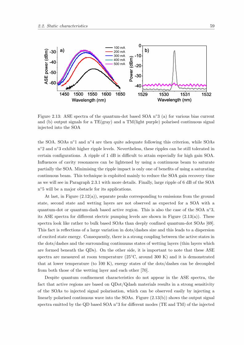
2.2. Static characteristics 59
1529 1530 1531 1532
-40
-30
-20
-10
0
Pow
er (d
Bm
)
Wavelength (nm)1450 1500 1550 1600 1650
-60
-50
-40
-30A
SE
pow
er (d
Bm
)
Wavelength (nm)
100 mA 200 mA 300 mA 400 mA 500 mA
a) b)
1529 1530 1531 1532
-40
-30
-20
-10
0
Pow
er (d
Bm
)
Wavelength (nm)1450 1500 1550 1600 1650
-60
-50
-40
-30A
SE
pow
er (d
Bm
)
Wavelength (nm)
100 mA 200 mA 300 mA 400 mA 500 mA
a) b)
Figure 2.13: ASE spectra of the quantum-dot based SOA n◦3 (a) for various bias currentand (b) output signals for a TE(gray) and a TM(light purple) polarised continuous signalinjected into the SOA
the SOA. SOAs n◦1 and n◦4 are then quite adequate following this criterion, while SOAs
n◦2 and n◦3 exhibit higher ripple levels. Nevertheless, these ripples can be still tolerated in
certain configurations. A ripple of 1 dB is difficult to attain especially for high gain SOA.
Influences of cavity resonances can be lightened by using a continuous beam to saturate
partially the SOA. Minimising the ripple impact is only one of benefits of using a saturating
continuous beam. This technique is exploited mainly to reduce the SOA gain recovery time
as we will see in Paragraph 2.3.1 with more details. Finally, large ripple of 6 dB of the SOA
n◦5 will be a major obstacle for its applications.
At last, in Figure (2.12(a)), separate peaks corresponding to emissions from the ground
state, second state and wetting layers are not observed as expected for a SOA with a
quantum-dot or quantum-dash based active region. This is also the case of the SOA n◦3,
its ASE spectra for different electric pumping levels are shown in Figure (2.13(a)). These
spectra look like rather to bulk based SOAs than deeply confined quantum-dot SOAs [69].
This fact is reflections of a large variation in dots/dashes size and this leads to a dispersion
of excited state energy. Consequently, there is a strong coupling between the active states in
the dots/dashes and the surrounding continuums states of wetting layers (thin layers which
are formed beneath the QDs). On the other side, it is important to note that these ASE
spectra are measured at room temperature (25◦C, around 300 K) and it is demonstrated
that at lower temperature (to 100 K), energy states of the dots/dashes can be decoupled
from both those of the wetting layer and each other [70].
Despite quantum confinement characteristics do not appear in the ASE spectra, the
fact that active regions are based on QDot/Qdash materials results in a strong sensitivity
of the SOAs to injected signal polarisation, which can be observed easily by injecting a
linearly polarised continuous wave into the SOAs. Figure (2.13(b)) shows the output signal
spectra emitted by the QD based SOA n◦3 for different modes (TE and TM) of the injected
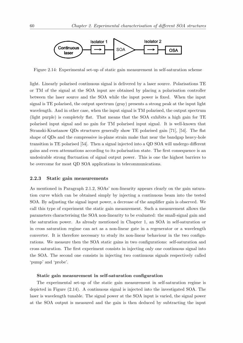
60 Chapter 2. Experimental characterisation of different SOA structures
OSAContinuouslaser
SOA
Isolator 1 Isolator 2
OSAContinuouslaser
SOA OSAContinuouslaser
Continuouslaser
SOASOA
Isolator 1 Isolator 2
Figure 2.14: Experimental set-up of static gain measurement in self-saturation scheme
light. Linearly polarised continuous signal is delivered by a laser source. Polarisations TE
or TM of the signal at the SOA input are obtained by placing a polarisation controller
between the laser source and the SOA while the input power is fixed. When the input
signal is TE polarised, the output spectrum (gray) presents a strong peak at the input light
wavelength. And in other case, when the input signal is TM polarised, the output spectrum
(light purple) is completely flat. That means that the SOA exhibits a high gain for TE
polarised input signal and no gain for TM polarised input signal. It is well-known that
Stranski-Krastanow QDs structures generally show TE polarised gain [71], [54]. The flat
shape of QDs and the compressive in-plane strain make that near the bandgap heavy-hole
transition is TE polarised [54]. Then a signal injected into a QD SOA will undergo different
gains and even attenuations according to its polarisation state. The first consequence is an
undesirable strong fluctuation of signal output power. This is one the highest barriers to
be overcome for most QD SOA applications in telecommunications.
2.2.3 Static gain measurements
As mentioned in Paragraph 2.1.2, SOAs’ non-linearity appears clearly on the gain satura-
tion curve which can be obtained simply by injecting a continuous beam into the tested
SOA. By adjusting the signal input power, a decrease of the amplifier gain is observed. We
call this type of experiment the static gain measurement. Such a measurement allows the
parameters characterising the SOA non-linearity to be evaluated: the small-signal gain and
the saturation power. As already mentioned in Chapter 1, an SOA in self-saturation or
in cross saturation regime can act as a non-linear gate in a regenerator or a wavelength
converter. It is therefore necessary to study its non-linear behaviour in the two configu-
rations. We measure then the SOA static gains in two configurations: self-saturation and
cross saturation. The first experiment consists in injecting only one continuous signal into
the SOA. The second one consists in injecting two continuous signals respectively called
‘pump’ and ‘probe’.
Static gain measurement in self-saturation configuration
The experimental set-up of the static gain measurement in self-saturation regime is
depicted in Figure (2.14). A continuous signal is injected into the investigated SOA. The
laser is wavelength tunable. The signal power at the SOA input is varied, the signal power
at the SOA output is measured and the gain is then deduced by subtracting the input
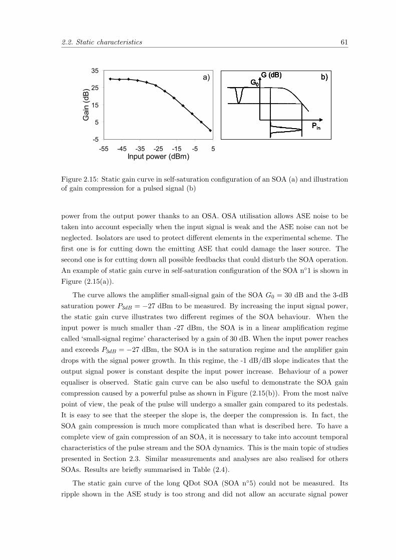
2.2. Static characteristics 61
-5
5
15
25
35
-55 -45 -35 -25 -15 -5 5Input power (dBm)
Gai
n (d
B)a)
Pin
G (dB)G0
b)
-5
5
15
25
35
-55 -45 -35 -25 -15 -5 5Input power (dBm)
Gai
n (d
B)a)
-5
5
15
25
35
-55 -45 -35 -25 -15 -5 5Input power (dBm)
Gai
n (d
B)a)
Pin
G (dB)G0
b)
Pin
G (dB)G0
Pin
G (dB)G0
Pin
G (dB)G0
Pin
G (dB)G0
b)
Figure 2.15: Static gain curve in self-saturation configuration of an SOA (a) and illustrationof gain compression for a pulsed signal (b)
power from the output power thanks to an OSA. OSA utilisation allows ASE noise to be
taken into account especially when the input signal is weak and the ASE noise can not be
neglected. Isolators are used to protect different elements in the experimental scheme. The
first one is for cutting down the emitting ASE that could damage the laser source. The
second one is for cutting down all possible feedbacks that could disturb the SOA operation.
An example of static gain curve in self-saturation configuration of the SOA n◦1 is shown in
Figure (2.15(a)).
The curve allows the amplifier small-signal gain of the SOA G0 = 30 dB and the 3-dB
saturation power P3dB = −27 dBm to be measured. By increasing the input signal power,
the static gain curve illustrates two different regimes of the SOA behaviour. When the
input power is much smaller than -27 dBm, the SOA is in a linear amplification regime
called ‘small-signal regime’ characterised by a gain of 30 dB. When the input power reaches
and exceeds P3dB = −27 dBm, the SOA is in the saturation regime and the amplifier gain
drops with the signal power growth. In this regime, the -1 dB/dB slope indicates that the
output signal power is constant despite the input power increase. Behaviour of a power
equaliser is observed. Static gain curve can be also useful to demonstrate the SOA gain
compression caused by a powerful pulse as shown in Figure (2.15(b)). From the most naıve
point of view, the peak of the pulse will undergo a smaller gain compared to its pedestals.
It is easy to see that the steeper the slope is, the deeper the compression is. In fact, the
SOA gain compression is much more complicated than what is described here. To have a
complete view of gain compression of an SOA, it is necessary to take into account temporal
characteristics of the pulse stream and the SOA dynamics. This is the main topic of studies
presented in Section 2.3. Similar measurements and analyses are also realised for others
SOAs. Results are briefly summarised in Table (2.4).
The static gain curve of the long QDot SOA (SOA n◦5) could not be measured. Its
ripple shown in the ASE study is too strong and did not allow an accurate signal power
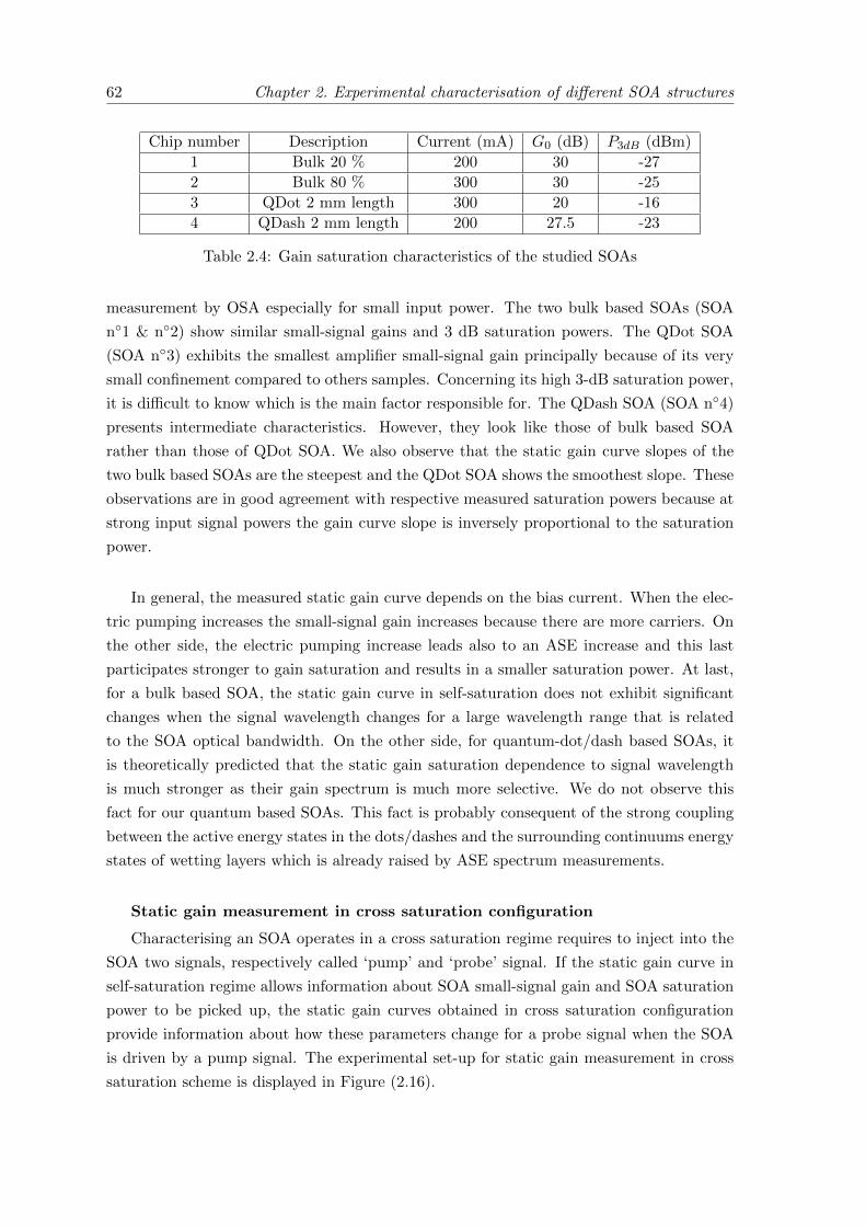
62 Chapter 2. Experimental characterisation of different SOA structures
Chip number Description Current (mA) G0 (dB) P3dB (dBm)
1 Bulk 20 % 200 30 -27
2 Bulk 80 % 300 30 -25
3 QDot 2 mm length 300 20 -16
4 QDash 2 mm length 200 27.5 -23
Table 2.4: Gain saturation characteristics of the studied SOAs
measurement by OSA especially for small input power. The two bulk based SOAs (SOA
n◦1 & n◦2) show similar small-signal gains and 3 dB saturation powers. The QDot SOA
(SOA n◦3) exhibits the smallest amplifier small-signal gain principally because of its very
small confinement compared to others samples. Concerning its high 3-dB saturation power,
it is difficult to know which is the main factor responsible for. The QDash SOA (SOA n◦4)
presents intermediate characteristics. However, they look like those of bulk based SOA
rather than those of QDot SOA. We also observe that the static gain curve slopes of the
two bulk based SOAs are the steepest and the QDot SOA shows the smoothest slope. These
observations are in good agreement with respective measured saturation powers because at
strong input signal powers the gain curve slope is inversely proportional to the saturation
power.
In general, the measured static gain curve depends on the bias current. When the elec-
tric pumping increases the small-signal gain increases because there are more carriers. On
the other side, the electric pumping increase leads also to an ASE increase and this last
participates stronger to gain saturation and results in a smaller saturation power. At last,
for a bulk based SOA, the static gain curve in self-saturation does not exhibit significant
changes when the signal wavelength changes for a large wavelength range that is related
to the SOA optical bandwidth. On the other side, for quantum-dot/dash based SOAs, it
is theoretically predicted that the static gain saturation dependence to signal wavelength
is much stronger as their gain spectrum is much more selective. We do not observe this
fact for our quantum based SOAs. This fact is probably consequent of the strong coupling
between the active energy states in the dots/dashes and the surrounding continuums energy
states of wetting layers which is already raised by ASE spectrum measurements.
Static gain measurement in cross saturation configuration
Characterising an SOA operates in a cross saturation regime requires to inject into the
SOA two signals, respectively called ‘pump’ and ‘probe’ signal. If the static gain curve in
self-saturation regime allows information about SOA small-signal gain and SOA saturation
power to be picked up, the static gain curves obtained in cross saturation configuration
provide information about how these parameters change for a probe signal when the SOA
is driven by a pump signal. The experimental set-up for static gain measurement in cross
saturation scheme is displayed in Figure (2.16).
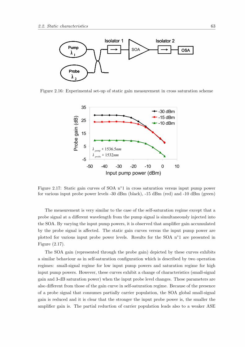
2.2. Static characteristics 63
OSASOAPump
1λ
2λProbe
Isolator 1 Isolator 2
OSASOAPump
1λ
2λProbe
OSASOASOAPump
1λPumpPump
1λ
2λProbe
2λProbeProbe
Isolator 1 Isolator 2
Figure 2.16: Experimental set-up of static gain measurement in cross saturation scheme
-5
5
15
25
35
-50 -40 -30 -20 -10 0 10Input pump power (dBm)
Pro
be g
ain
(dB
)
-30 dBm-15 dBm-10 dBm
nmpump 5.1536=λnmprobe 1532=λ
-5
5
15
25
35
-50 -40 -30 -20 -10 0 10Input pump power (dBm)
Pro
be g
ain
(dB
)
-30 dBm-15 dBm-10 dBm
nmpump 5.1536=λnmprobe 1532=λ
Figure 2.17: Static gain curves of SOA n◦1 in cross saturation versus input pump powerfor various input probe power levels -30 dBm (black), -15 dBm (red) and -10 dBm (green)
The measurement is very similar to the case of the self-saturation regime except that a
probe signal at a different wavelength from the pump signal is simultaneously injected into
the SOA. By varying the input pump powers, it is observed that amplifier gain accumulated
by the probe signal is affected. The static gain curves versus the input pump power are
plotted for various input probe power levels. Results for the SOA n◦1 are presented in
Figure (2.17).
The SOA gain (represented through the probe gain) depicted by these curves exhibits
a similar behaviour as in self-saturation configuration which is described by two operation
regimes: small-signal regime for low input pump powers and saturation regime for high
input pump powers. However, these curves exhibit a change of characteristics (small-signal
gain and 3-dB saturation power) when the input probe level changes. These parameters are
also different from those of the gain curve in self-saturation regime. Because of the presence
of a probe signal that consumes partially carrier population, the SOA global small-signal
gain is reduced and it is clear that the stronger the input probe power is, the smaller the
amplifier gain is. The partial reduction of carrier population leads also to a weaker ASE
64 Chapter 2. Experimental characterisation of different SOA structures
noise and a direct consequent is a higher saturation power. At last, it is interesting to
note that for small input powers such that pump signal can be neglected compared to the
probe signal, gain self-saturation caused by the probe signal can be observed. Amplifier gain
drops from 29 dB to 10 dB when the input probe power increases from -30 dBm to -10 dBm.
All static characterisations must not be skipped. They provide primary and practical
information about an SOA. P(I) measurement allows to determine the maximum bias cur-
rent supported by the SOA. The study of the ASE spectra allows the adequate operating
wavelength range and the gain ripple level to be determined. At last, static gain curves
gives information about the SOA gain non-linearity in different operating situations: self-
saturation and cross saturation. SOA parameters achieved through these characterisations
are primordial to evaluate if the SOA could be used as a non-linear gate in signal processing
applications. The SOA should exhibit a high small-signal gain, small ripple, low satura-
tion power and a steep slope of static gain curve. Furthermore, these characteristics allow
operation of any concrete application scheme based on the tested SOA to be optimised.
Once static characterisations are realised, the SOA dynamics must to be investigated
because they define the limit operating bit rate of an SOA based regenerator or wavelength
converter.
2.3. Dynamics characterisation 65
2.3 Dynamics characterisation
SOAs have been used in several optical transmission experiments with good performance.
In applications such pre-amplification, the amplifier is operated mostly in the linear regime
in which the amplified pulse is a replica of the input pulse. However, in a large number
of other applications such optical logical gates, optical clock recovery and especially in
wavelength converters and regenerators, the amplifier is used as a non-linear optical gate
which implies operating in saturation regime. When the SOA is saturated by a pulsed
signal, its optical gain becomes time dependent, which means also a time dependence of
the refractive index. This may be viewed simply as follows. The gain saturation leads to
a change in carrier density which results in a change in refractive index and then of the
signal phase. These SOA gain and phase dynamics are important for SOA based non-linear
optical gates.
SOA based wavelength conversion and regeneration schemes exploit gain modulation,
cross phase modulation or four wave mixing. When the gain modulation is used, attention
must be paid to the gain recovery time of the SOA. On the other side, in interferometer
configurations which exploit simultaneously gain and phase modulations, both gain and
phase dynamics should be considered. Gain and phase recovery times are key parameters
which determine patterning effects and the bit rate limit at which the SOA could be oper-
ated. SOA gain and phase dynamics can be measured by exploiting pump-probe technique
with two types of experiment. The first one is a degenerate pump-probe experiment us-
ing pulse streams at low repetition rate (below 100 MHz), with heterodyne detection and
femtosecond time resolution [60], [72]. The second one is a usual wavelength conversion
configuration using pulse streams at high repetition rate (up to 40 GHz), with picosecond
time resolution [64]. The dynamics experiment with femtosecond pulses offers a high time
resolution measurement and allows different characteristic time constants of the SOA to be
identified. The second dynamics experiment with picosecond pulses at high repetition rate
is useful to understand how external operating parameters (signal wavelength, pulsewidth,
data rate...) influence the SOA dynamics as the SOA is operated under conditions that are
very similar to those of actual backbone transmissions.
In order to find adequate SOAs that could be used in a wavelength converter or in an
all-optical regenerator for ultrahigh bit rate transmission, we elaborate in our laboratory a
gain dynamics measurement based on wavelength conversion scheme with picosecond time
resolution as presented in Paragraph 2.3.1. Phase dynamics measurement has been not
possible yet but it could be elaborated by using an interferometer. This Section 2.3 is
dedicated to gain dynamics experiment presentation and experimental results obtained for
various SOAs. Impacts of operating conditions such as signals pulsewidth and wavelength,
bias current, waveguide length and output filtering are investigated.
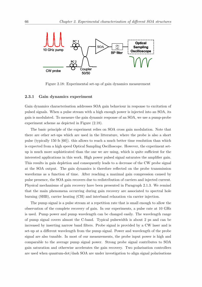
66 Chapter 2. Experimental characterisation of different SOA structures
Coupler 50/50
10 GHz pumpSOA
CW probe
PC 1
PC 2
BP filter
Optical Sampling
Oscilloscope
Coupler 50/50
10 GHz pumpSOA
CW probe
PC 1PC 1
PC 2PC 2PC 2
BP filterBP filter
Optical Sampling
Oscilloscope
Figure 2.18: Experimental set-up of gain dynamics measurement
2.3.1 Gain dynamics experiment
Gain dynamics characterisation addresses SOA gain behaviour in response to excitation of
pulsed signals. When a pulse stream with a high enough power is injected into an SOA, its
gain is modulated. To measure the gain dynamic response of an SOA, we use a pump-probe
experiment scheme as depicted in Figure (2.18).
The basic principle of the experiment relies on SOA cross gain modulation. Note that
there are other set-ups which are used in the litterature, where the probe is also a short
pulse (typically 150 fs [60]). this allows to reach a much better time resolution than which
is expected from a high speed Optical Sampling Oscilloscope. However, the experiment set-
up is much more sophisticated than the one we are using, which is quite sufficient for the
interested applications in this work. High power pulsed signal saturates the amplifier gain.
This results in gain depletion and consequently leads to a decrease of the CW probe signal
at the SOA output. The gain dynamics is therefore reflected on the probe transmission
waveforms as a function of time. After reaching a maximal gain compression caused by
pulse presence, the SOA gain recovers due to redistribution of carriers and injected current.
Physical mechanisms of gain recovery have been presented in Paragraph 2.1.3. We remind
that the main phenomena occurring during gain recovery are associated to spectral hole
burning (SHB), carrier heating (CH) and interband relaxation via carrier injection.
The pump signal is a pulse stream at a repetition rate that is small enough to allow the
observation of the complete recovery of gain. In our experiments, a pulse rate at 10 GHz
is used. Pump power and pump wavelength can be changed easily. The wavelength range
of pump signal covers almost the C-band. Typical pulsewidth is about 2 ps and can be
increased by inserting narrow band filters. Probe signal is provided by a CW laser and is
set-up at a different wavelength from the pump signal. Power and wavelength of the probe
signal are also tunable. In most of our measurements, the probe input power is high and
comparable to the average pump signal power. Strong probe signal contributes to SOA
gain saturation and otherwise accelerates the gain recovery. Two polarisation controllers
are used when quantum-dot/dash SOA are under investigation to align signal polarisations
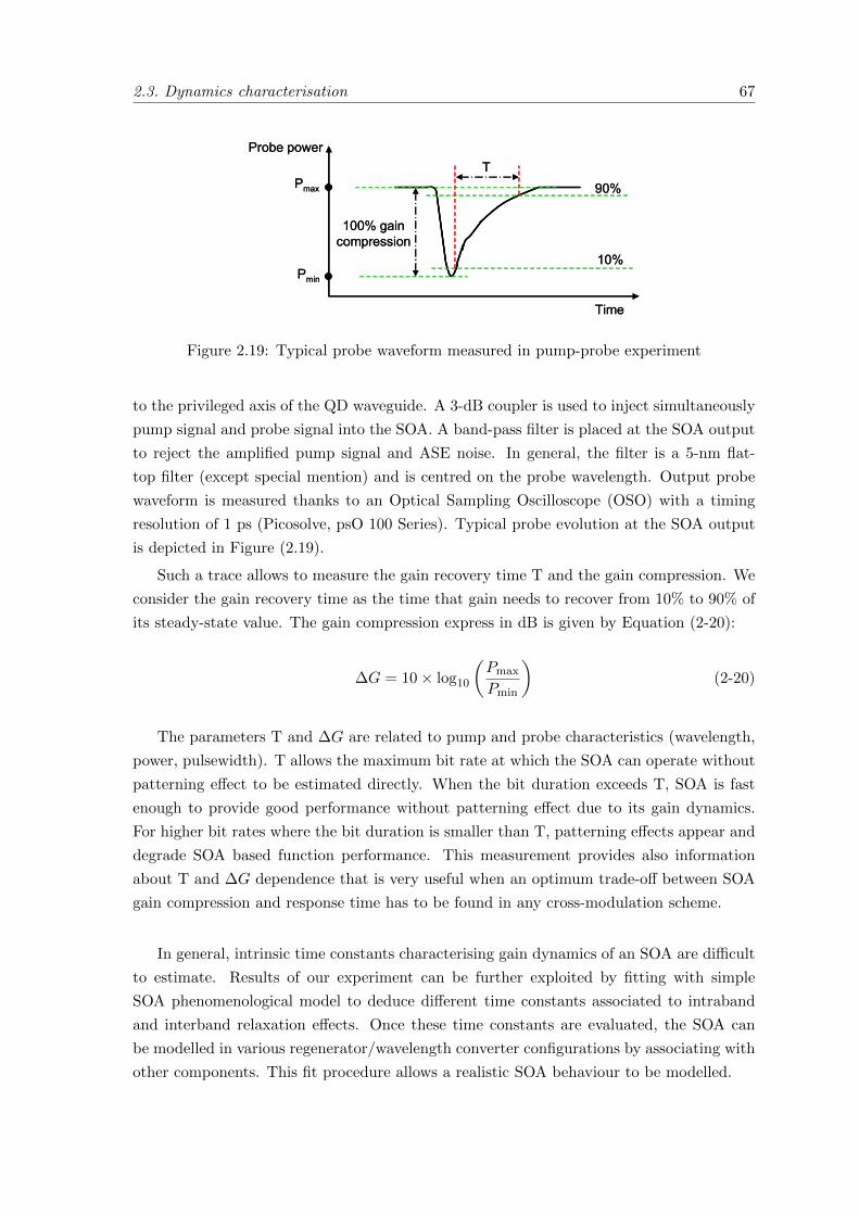
2.3. Dynamics characterisation 67
100% gain compression
90%
10%
T
Time
Probe power
Pmax
Pmin
100% gain compression
90%
10%
T
Time
Probe power
Pmax
Pmin
Figure 2.19: Typical probe waveform measured in pump-probe experiment
to the privileged axis of the QD waveguide. A 3-dB coupler is used to inject simultaneously
pump signal and probe signal into the SOA. A band-pass filter is placed at the SOA output
to reject the amplified pump signal and ASE noise. In general, the filter is a 5-nm flat-
top filter (except special mention) and is centred on the probe wavelength. Output probe
waveform is measured thanks to an Optical Sampling Oscilloscope (OSO) with a timing
resolution of 1 ps (Picosolve, psO 100 Series). Typical probe evolution at the SOA output
is depicted in Figure (2.19).
Such a trace allows to measure the gain recovery time T and the gain compression. We
consider the gain recovery time as the time that gain needs to recover from 10% to 90% of
its steady-state value. The gain compression express in dB is given by Equation (2-20):
∆G = 10× log10
(Pmax
Pmin
)(2-20)
The parameters T and ∆G are related to pump and probe characteristics (wavelength,
power, pulsewidth). T allows the maximum bit rate at which the SOA can operate without
patterning effect to be estimated directly. When the bit duration exceeds T, SOA is fast
enough to provide good performance without patterning effect due to its gain dynamics.
For higher bit rates where the bit duration is smaller than T, patterning effects appear and
degrade SOA based function performance. This measurement provides also information
about T and ∆G dependence that is very useful when an optimum trade-off between SOA
gain compression and response time has to be found in any cross-modulation scheme.
In general, intrinsic time constants characterising gain dynamics of an SOA are difficult
to estimate. Results of our experiment can be further exploited by fitting with simple
SOA phenomenological model to deduce different time constants associated to intraband
and interband relaxation effects. Once these time constants are evaluated, the SOA can
be modelled in various regenerator/wavelength converter configurations by associating with
other components. This fit procedure allows a realistic SOA behaviour to be modelled.
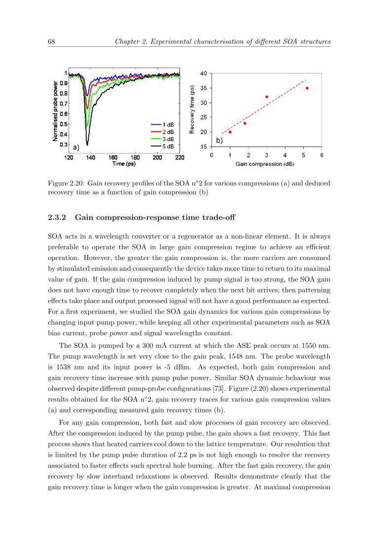
68 Chapter 2. Experimental characterisation of different SOA structures
Figure 2.20: Gain recovery profiles of the SOA n◦2 for various compressions (a) and deducedrecovery time as a function of gain compression (b)
2.3.2 Gain compression-response time trade-off
SOA acts in a wavelength converter or a regenerator as a non-linear element. It is always
preferable to operate the SOA in large gain compression regime to achieve an efficient
operation. However, the greater the gain compression is, the more carriers are consumed
by stimulated emission and consequently the device takes more time to return to its maximal
value of gain. If the gain compression induced by pump signal is too strong, the SOA gain
does not have enough time to recover completely when the next bit arrives; then patterning
effects take place and output processed signal will not have a good performance as expected.
For a first experiment, we studied the SOA gain dynamics for various gain compressions by
changing input pump power, while keeping all other experimental parameters such as SOA
bias current, probe power and signal wavelengths constant.
The SOA is pumped by a 300 mA current at which the ASE peak occurs at 1550 nm.
The pump wavelength is set very close to the gain peak, 1548 nm. The probe wavelength
is 1538 nm and its input power is -5 dBm. As expected, both gain compression and
gain recovery time increase with pump pulse power. Similar SOA dynamic behaviour was
observed despite different pump-probe configurations [73]. Figure (2.20) shows experimental
results obtained for the SOA n◦2, gain recovery traces for various gain compression values
(a) and corresponding measured gain recovery times (b).
For any gain compression, both fast and slow processes of gain recovery are observed.
After the compression induced by the pump pulse, the gain shows a fast recovery. This fast
process shows that heated carriers cool down to the lattice temperature. Our resolution that
is limited by the pump pulse duration of 2.2 ps is not high enough to resolve the recovery
associated to faster effects such spectral hole burning. After the fast gain recovery, the gain
recovery by slow interband relaxations is observed. Results demonstrate clearly that the
gain recovery time is longer when the gain compression is greater. At maximal compression
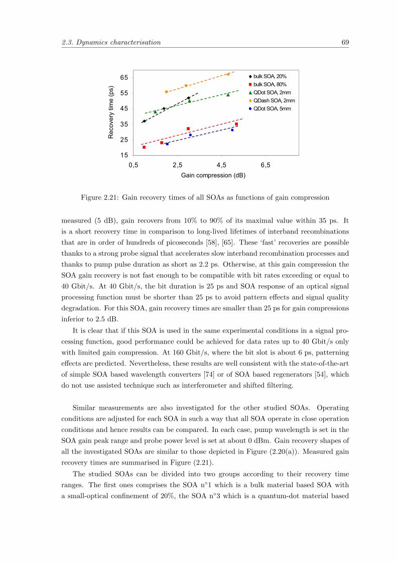
2.3. Dynamics characterisation 69
15
25
35
45
55
65
0,5 2,5 4,5 6,5Gain compression (dB)
Rec
over
y tim
e (p
s)
bulk SOA, 20%bulk SOA, 80%QDot SOA, 2mmQDash SOA, 2mmQDot SOA, 5mm
Figure 2.21: Gain recovery times of all SOAs as functions of gain compression
measured (5 dB), gain recovers from 10% to 90% of its maximal value within 35 ps. It
is a short recovery time in comparison to long-lived lifetimes of interband recombinations
that are in order of hundreds of picoseconds [58], [65]. These ‘fast’ recoveries are possible
thanks to a strong probe signal that accelerates slow interband recombination processes and
thanks to pump pulse duration as short as 2.2 ps. Otherwise, at this gain compression the
SOA gain recovery is not fast enough to be compatible with bit rates exceeding or equal to
40 Gbit/s. At 40 Gbit/s, the bit duration is 25 ps and SOA response of an optical signal
processing function must be shorter than 25 ps to avoid pattern effects and signal quality
degradation. For this SOA, gain recovery times are smaller than 25 ps for gain compressions
inferior to 2.5 dB.
It is clear that if this SOA is used in the same experimental conditions in a signal pro-
cessing function, good performance could be achieved for data rates up to 40 Gbit/s only
with limited gain compression. At 160 Gbit/s, where the bit slot is about 6 ps, patterning
effects are predicted. Nevertheless, these results are well consistent with the state-of-the-art
of simple SOA based wavelength converters [74] or of SOA based regenerators [54], which
do not use assisted technique such as interferometer and shifted filtering.
Similar measurements are also investigated for the other studied SOAs. Operating
conditions are adjusted for each SOA in such a way that all SOA operate in close operation
conditions and hence results can be compared. In each case, pump wavelength is set in the
SOA gain peak range and probe power level is set at about 0 dBm. Gain recovery shapes of
all the investigated SOAs are similar to those depicted in Figure (2.20(a)). Measured gain
recovery times are summarised in Figure (2.21).
The studied SOAs can be divided into two groups according to their recovery time
ranges. The first ones comprises the SOA n◦1 which is a bulk material based SOA with
a small-optical confinement of 20%, the SOA n◦3 which is a quantum-dot material based
70 Chapter 2. Experimental characterisation of different SOA structures
SOA with a waveguide length of 2 mm and the SOA n◦4 which is a quantum-dash material
based SOA with the same length of 2 mm. These SOAs show long recovery times of at least
35 ps even for gain compression as low as 1 dB. They will be not efficient for operation at
the bit rate of 40 Gbit/s and higher. Large patterning effects will degrade signal quality.
The second group comprises the SOA n◦2, which is a bulk based SOA with a high optical
confinement of 80% and the SOA n◦5, which is a quantum-dot material based SOA with
a ultralong waveguide of 5 mm. These samples exhibit recovery times as low as 25 ps for
gain compressions of about 2.5 dB. This result shows a potential of the two components for
non-linear optical gates operating at 40 Gbit/s. By using techniques such as interferometer
configurations or shifted filtering, operation at 160 Gbit/s can be expected.
As far as bulk based components are concerned, even if the two components are based
on the same material and the waveguides have the same length, they display very different
dynamics. The SOA n◦2 appears much faster than the SOA n◦1. This dynamics difference
results mainly from the different optical confinement factors (20% for the n◦1 and 80% for
the n◦2) and can be viewed as follow. In presence of intense photon density, carrier recovery
process is characterised by an effective carrier lifetime τe that is defined by Equation (2-
21) [66]:
1
τe=
1
τ+
1
τ ′(2-21)
τ is the intrinsic carrier lifetime and τ ′ is due to stimulated emission. The first term τ is
intrinsic to the SOA material. For the two bulk material based SOAs, this term is the same
because both SOA active regions are constituted of InGaAsP material. The second term
τ ′ is inversely proportional to the SOA confinement factor. It is evident that the effective
carrier lifetime τe can be decreased by reducing τ ′. On the other side, τ ′ reducing can
be achieved by increasing the optical confinement. Finally, the effective carrier lifetime is
smaller if the optical confinement is larger. Then, high confinement SOAs must be preferred
for ultrahigh bit rate functions thanks to faster effective dynamic response.
Concerning quantum material based SOAs, the quantum-dash based SOA displays a
slower gain recovery compared to the two quantum-dot based samples. This result is in
agreement with other experimental works reported in the literature [75], [65]. In our ex-
periment, the 2-mm QDash device (SOA n◦4) and the 2-mm QDot device (SOA n◦3) were
pumped at the same current density and probe powers were nearly identical. Different gain
recovery speeds reflects therefore the difference of intrinsic dynamics of the two devices. At
3 dB of gain compression, QDot SOA shows a recovery time of 50 ps and this time is raised
to 60 ps for the QDash sample. It is shown that in gain regime, short lifetimes associated
to ultrafast processes such as SHB and CH are similar for QDot and QDash based SOAs.
The SHB and CH physical mechanisms are independent of the degree of quantum confine-
ment. On the contrary, the degree of quantum confinement leads to a significant difference
of long lifetimes of the two SOAs. The dynamics behaviour of QDash SOA is considered
2.3. Dynamics characterisation 71
similar to that of a wire like quantum confinement (1-D). Because capture processes are
faster for higher quantum-confined material, QDot SOAs (0-D) exhibit therefore a shorter
long-lived lifetime [65]. Then the global gain recovery time in a QDot SOA is shorter than
in a QDash SOA. This result indicates that QDot SOA is the most promising for ultrafast
signal processing functions.
At last, comparing the two quantum-dot based SOAs, it is observed that recovery times
drop drastically from about 50 ps for the 2-mm QDot SOA to about 25 ps for the 5-mm
QDot SOA. If the short QDot SOA exhibits too slow response to be used at 40 Gbit/s, the
use of the long QDot SOA appears possible under small gain compression. Dimensions of
the two SOA structures are different, especially the active region length. An explanation of
this difference will be presented later in Paragraph 2.3.5. However, a qualitative explanation
can be given as follows. Amplifier length can affect SOA gain dynamics [76], [77], [78], [79].
In long devices, ASE propagation in an SOA can not be neglected anymore. ASE induces
stimulated emission recombination and hence speed up gain recovery dynamics. By increas-
ing the SOA length, not only the amplifier gain is increased but also the ASE power and
the last can shorten gain recovery [76].
The results show that even if gain recovery of all SOAs exhibits partially ultrafast pro-
cesses, they are not all suitable for signal processing function at 40 Gbit/s and higher. Only
the SOA n◦2 and the SOA n◦5 show recovery times as short as 25 ps at a gain compres-
sion of 2.5 dB and then are promising for operation at 40 Gbit/s and above. However, by
associating these SOAs with techniques such as shifted filtering or use in an interferometer
configuration, signal processing functions operating at 160 Gbit/s can be expected. Gain
recovery durations can be shortened by decreasing the gain compression but this fact can
limit efficiency of the SOA used as a non-linear element. Depending on specific signal pro-
cessing function, a trade-off between gain compression and response time of the SOA must
be found to obtain the best performance of a regenerator or a wavelength converter. It ap-
pears also that by increasing optical confinement and waveguide length, SOA gain recovery
dynamics can be enhanced. Therefore highly confined and longer SOA are preferable for
signal processing at ultrahigh bit rate. At last, in spite of very small confinement factor
(1%), quantum-dot based SOAs demonstrate gain dynamics as fast as highly confined bulk
based SOA. This ultrafast carrier dynamics of QD SOA is one of the advantages offered by
quantum confined material.
2.3.3 Impact of bias current
Despite the presence of an ultrafast contribution in gain recovery processes under saturation
by pump pulses as short as 2 ps, applications of SOAs in signal processing at 40 Gbit/s and
higher are still limited especially in functions exploiting gain modulation. SOA response
remains ‘too long’ compared to bit slot of 25 ps because of the slow recovery component that
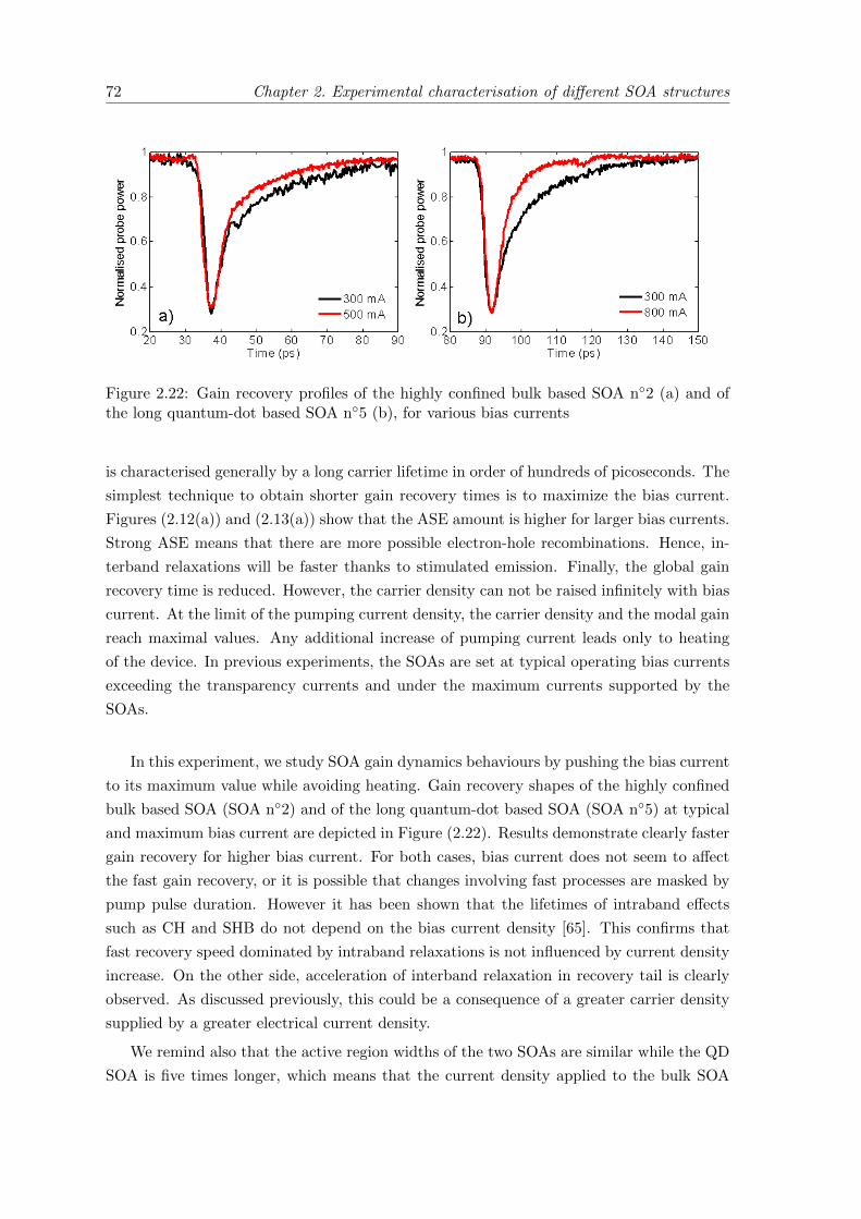
72 Chapter 2. Experimental characterisation of different SOA structures
Figure 2.22: Gain recovery profiles of the highly confined bulk based SOA n◦2 (a) and ofthe long quantum-dot based SOA n◦5 (b), for various bias currents
is characterised generally by a long carrier lifetime in order of hundreds of picoseconds. The
simplest technique to obtain shorter gain recovery times is to maximize the bias current.
Figures (2.12(a)) and (2.13(a)) show that the ASE amount is higher for larger bias currents.
Strong ASE means that there are more possible electron-hole recombinations. Hence, in-
terband relaxations will be faster thanks to stimulated emission. Finally, the global gain
recovery time is reduced. However, the carrier density can not be raised infinitely with bias
current. At the limit of the pumping current density, the carrier density and the modal gain
reach maximal values. Any additional increase of pumping current leads only to heating
of the device. In previous experiments, the SOAs are set at typical operating bias currents
exceeding the transparency currents and under the maximum currents supported by the
SOAs.
In this experiment, we study SOA gain dynamics behaviours by pushing the bias current
to its maximum value while avoiding heating. Gain recovery shapes of the highly confined
bulk based SOA (SOA n◦2) and of the long quantum-dot based SOA (SOA n◦5) at typical
and maximum bias current are depicted in Figure (2.22). Results demonstrate clearly faster
gain recovery for higher bias current. For both cases, bias current does not seem to affect
the fast gain recovery, or it is possible that changes involving fast processes are masked by
pump pulse duration. However it has been shown that the lifetimes of intraband effects
such as CH and SHB do not depend on the bias current density [65]. This confirms that
fast recovery speed dominated by intraband relaxations is not influenced by current density
increase. On the other side, acceleration of interband relaxation in recovery tail is clearly
observed. As discussed previously, this could be a consequence of a greater carrier density
supplied by a greater electrical current density.
We remind also that the active region widths of the two SOAs are similar while the QD
SOA is five times longer, which means that the current density applied to the bulk SOA
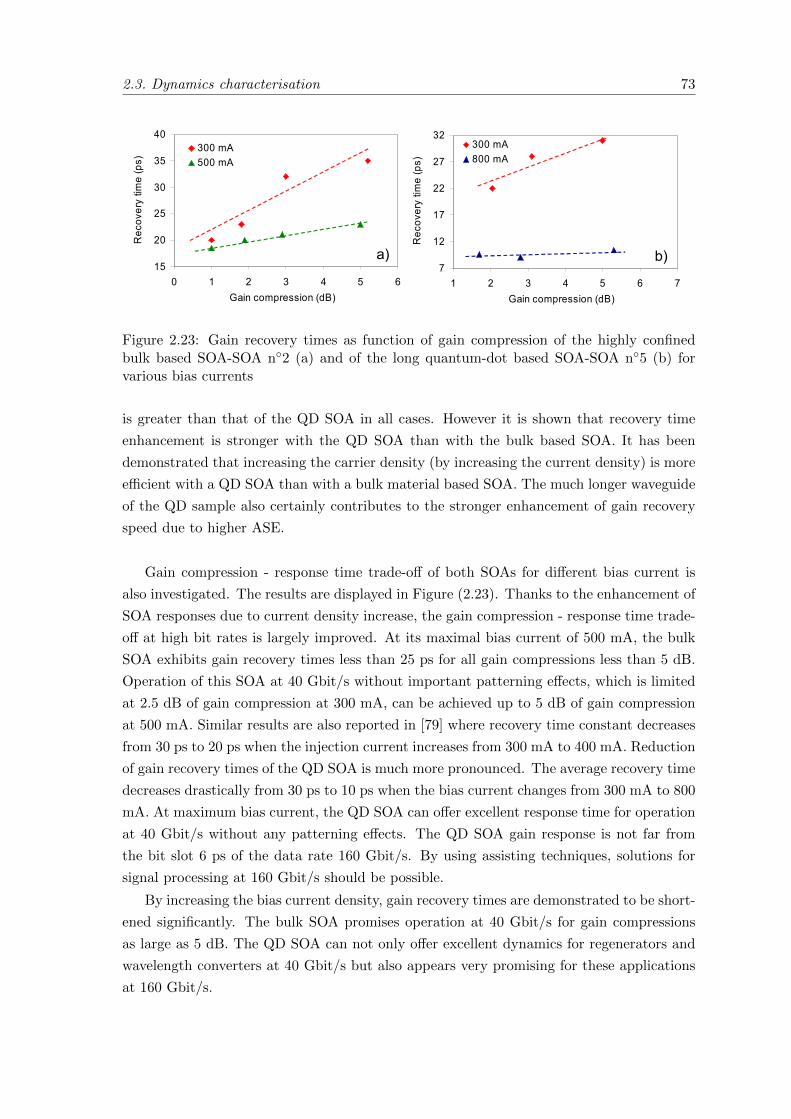
2.3. Dynamics characterisation 73
7
12
17
22
27
32
1 2 3 4 5 6 7Gain compression (dB)
Rec
over
y tim
e (p
s)
300 mA800 mA
15
20
25
30
35
40
0 1 2 3 4 5 6Gain compression (dB)
Rec
over
y tim
e (p
s)300 mA500 mA
a) b)7
12
17
22
27
32
1 2 3 4 5 6 7Gain compression (dB)
Rec
over
y tim
e (p
s)
300 mA800 mA
15
20
25
30
35
40
0 1 2 3 4 5 6Gain compression (dB)
Rec
over
y tim
e (p
s)300 mA500 mA
a) b)
Figure 2.23: Gain recovery times as function of gain compression of the highly confinedbulk based SOA-SOA n◦2 (a) and of the long quantum-dot based SOA-SOA n◦5 (b) forvarious bias currents
is greater than that of the QD SOA in all cases. However it is shown that recovery time
enhancement is stronger with the QD SOA than with the bulk based SOA. It has been
demonstrated that increasing the carrier density (by increasing the current density) is more
efficient with a QD SOA than with a bulk material based SOA. The much longer waveguide
of the QD sample also certainly contributes to the stronger enhancement of gain recovery
speed due to higher ASE.
Gain compression - response time trade-off of both SOAs for different bias current is
also investigated. The results are displayed in Figure (2.23). Thanks to the enhancement of
SOA responses due to current density increase, the gain compression - response time trade-
off at high bit rates is largely improved. At its maximal bias current of 500 mA, the bulk
SOA exhibits gain recovery times less than 25 ps for all gain compressions less than 5 dB.
Operation of this SOA at 40 Gbit/s without important patterning effects, which is limited
at 2.5 dB of gain compression at 300 mA, can be achieved up to 5 dB of gain compression
at 500 mA. Similar results are also reported in [79] where recovery time constant decreases
from 30 ps to 20 ps when the injection current increases from 300 mA to 400 mA. Reduction
of gain recovery times of the QD SOA is much more pronounced. The average recovery time
decreases drastically from 30 ps to 10 ps when the bias current changes from 300 mA to 800
mA. At maximum bias current, the QD SOA can offer excellent response time for operation
at 40 Gbit/s without any patterning effects. The QD SOA gain response is not far from
the bit slot 6 ps of the data rate 160 Gbit/s. By using assisting techniques, solutions for
signal processing at 160 Gbit/s should be possible.
By increasing the bias current density, gain recovery times are demonstrated to be short-
ened significantly. The bulk SOA promises operation at 40 Gbit/s for gain compressions
as large as 5 dB. The QD SOA can not only offer excellent dynamics for regenerators and
wavelength converters at 40 Gbit/s but also appears very promising for these applications
at 160 Gbit/s.
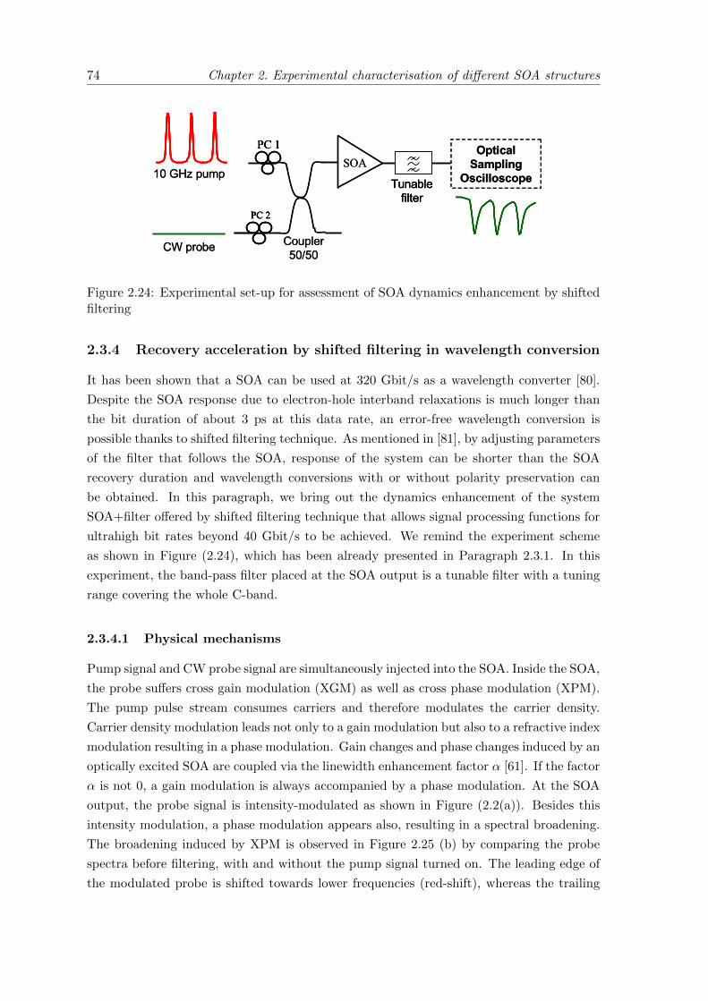
74 Chapter 2. Experimental characterisation of different SOA structures
Coupler 50/50
10 GHz pumpSOA
CW probe
PC 1
PC 2
Tunablefilter
Optical Sampling
Oscilloscope
Coupler 50/50
10 GHz pumpSOA
CW probe
PC 1PC 1
PC 2PC 2PC 2
Tunablefilter
Tunablefilter
Optical Sampling
Oscilloscope
Figure 2.24: Experimental set-up for assessment of SOA dynamics enhancement by shiftedfiltering
2.3.4 Recovery acceleration by shifted filtering in wavelength conversion
It has been shown that a SOA can be used at 320 Gbit/s as a wavelength converter [80].
Despite the SOA response due to electron-hole interband relaxations is much longer than
the bit duration of about 3 ps at this data rate, an error-free wavelength conversion is
possible thanks to shifted filtering technique. As mentioned in [81], by adjusting parameters
of the filter that follows the SOA, response of the system can be shorter than the SOA
recovery duration and wavelength conversions with or without polarity preservation can
be obtained. In this paragraph, we bring out the dynamics enhancement of the system
SOA+filter offered by shifted filtering technique that allows signal processing functions for
ultrahigh bit rates beyond 40 Gbit/s to be achieved. We remind the experiment scheme
as shown in Figure (2.24), which has been already presented in Paragraph 2.3.1. In this
experiment, the band-pass filter placed at the SOA output is a tunable filter with a tuning
range covering the whole C-band.
2.3.4.1 Physical mechanisms
Pump signal and CW probe signal are simultaneously injected into the SOA. Inside the SOA,
the probe suffers cross gain modulation (XGM) as well as cross phase modulation (XPM).
The pump pulse stream consumes carriers and therefore modulates the carrier density.
Carrier density modulation leads not only to a gain modulation but also to a refractive index
modulation resulting in a phase modulation. Gain changes and phase changes induced by an
optically excited SOA are coupled via the linewidth enhancement factor α [61]. If the factor
α is not 0, a gain modulation is always accompanied by a phase modulation. At the SOA
output, the probe signal is intensity-modulated as shown in Figure (2.2(a)). Besides this
intensity modulation, a phase modulation appears also, resulting in a spectral broadening.
The broadening induced by XPM is observed in Figure 2.25 (b) by comparing the probe
spectra before filtering, with and without the pump signal turned on. The leading edge of
the modulated probe is shifted towards lower frequencies (red-shift), whereas the trailing
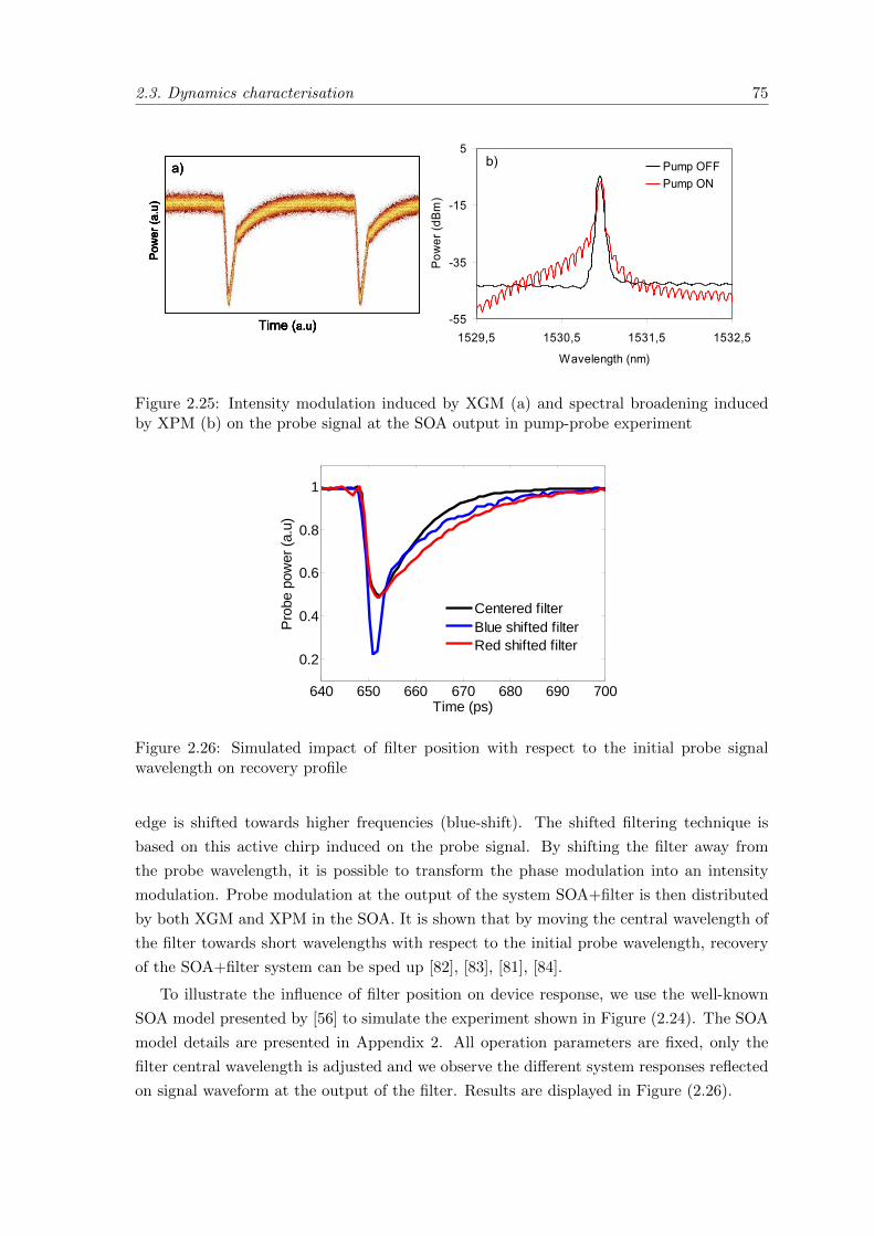
2.3. Dynamics characterisation 75
-55
-35
-15
5
1529,5 1530,5 1531,5 1532,5
Wavelength (nm)
Pow
er (d
Bm
)
Pump OFFPump ON
b)
Time (a.u)
Pow
er (a
.u)
a)
-55
-35
-15
5
1529,5 1530,5 1531,5 1532,5
Wavelength (nm)
Pow
er (d
Bm
)
Pump OFFPump ON
b)
Time (a.u)
Pow
er (a
.u)
a)
Time (a.u)
Pow
er (a
.u)
Time (a.u)
Pow
er (a
.u)
a)
Figure 2.25: Intensity modulation induced by XGM (a) and spectral broadening inducedby XPM (b) on the probe signal at the SOA output in pump-probe experiment
640 650 660 670 680 690 700
0.2
0.4
0.6
0.8
1
Time (ps)
Pro
be p
ower
(a.
u)
Centered filterBlue shifted filterRed shifted filter
Figure 2.26: Simulated impact of filter position with respect to the initial probe signalwavelength on recovery profile
edge is shifted towards higher frequencies (blue-shift). The shifted filtering technique is
based on this active chirp induced on the probe signal. By shifting the filter away from
the probe wavelength, it is possible to transform the phase modulation into an intensity
modulation. Probe modulation at the output of the system SOA+filter is then distributed
by both XGM and XPM in the SOA. It is shown that by moving the central wavelength of
the filter towards short wavelengths with respect to the initial probe wavelength, recovery
of the SOA+filter system can be sped up [82], [83], [81], [84].
To illustrate the influence of filter position on device response, we use the well-known
SOA model presented by [56] to simulate the experiment shown in Figure (2.24). The SOA
model details are presented in Appendix 2. All operation parameters are fixed, only the
filter central wavelength is adjusted and we observe the different system responses reflected
on signal waveform at the output of the filter. Results are displayed in Figure (2.26).
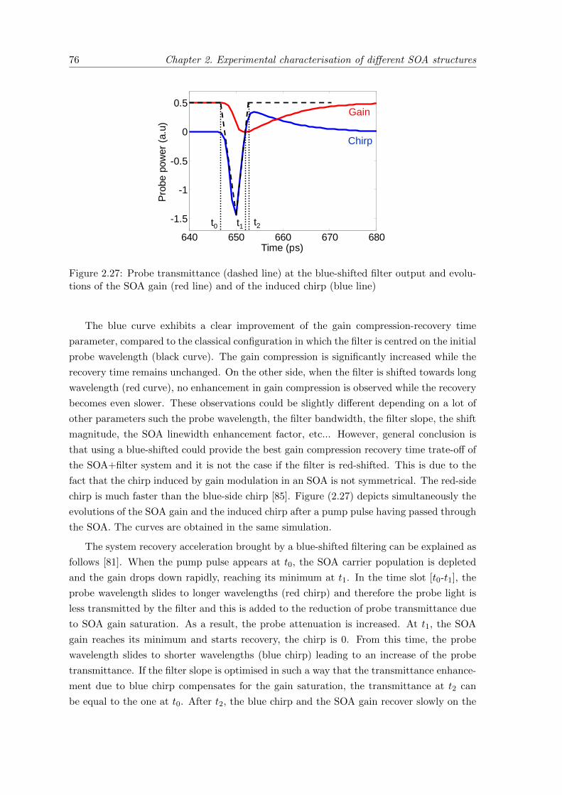
76 Chapter 2. Experimental characterisation of different SOA structures
640 650 660 670 680
-1.5
-1
-0.5
0
0.5
Time (ps)
Pro
be p
ower
(a.
u)
Gain
Chirp
t0 t1 t2
Figure 2.27: Probe transmittance (dashed line) at the blue-shifted filter output and evolu-tions of the SOA gain (red line) and of the induced chirp (blue line)
The blue curve exhibits a clear improvement of the gain compression-recovery time
parameter, compared to the classical configuration in which the filter is centred on the initial
probe wavelength (black curve). The gain compression is significantly increased while the
recovery time remains unchanged. On the other side, when the filter is shifted towards long
wavelength (red curve), no enhancement in gain compression is observed while the recovery
becomes even slower. These observations could be slightly different depending on a lot of
other parameters such the probe wavelength, the filter bandwidth, the filter slope, the shift
magnitude, the SOA linewidth enhancement factor, etc... However, general conclusion is
that using a blue-shifted could provide the best gain compression recovery time trate-off of
the SOA+filter system and it is not the case if the filter is red-shifted. This is due to the
fact that the chirp induced by gain modulation in an SOA is not symmetrical. The red-side
chirp is much faster than the blue-side chirp [85]. Figure (2.27) depicts simultaneously the
evolutions of the SOA gain and the induced chirp after a pump pulse having passed through
the SOA. The curves are obtained in the same simulation.
The system recovery acceleration brought by a blue-shifted filtering can be explained as
follows [81]. When the pump pulse appears at t0, the SOA carrier population is depleted
and the gain drops down rapidly, reaching its minimum at t1. In the time slot [t0-t1], the
probe wavelength slides to longer wavelengths (red chirp) and therefore the probe light is
less transmitted by the filter and this is added to the reduction of probe transmittance due
to SOA gain saturation. As a result, the probe attenuation is increased. At t1, the SOA
gain reaches its minimum and starts recovery, the chirp is 0. From this time, the probe
wavelength slides to shorter wavelengths (blue chirp) leading to an increase of the probe
transmittance. If the filter slope is optimised in such a way that the transmittance enhance-
ment due to blue chirp compensates for the gain saturation, the transmittance at t2 can
be equal to the one at t0. After t2, the blue chirp and the SOA gain recover slowly on the
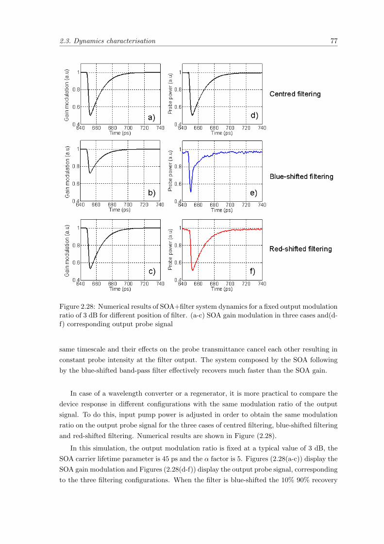
2.3. Dynamics characterisation 77
Figure 2.28: Numerical results of SOA+filter system dynamics for a fixed output modulationratio of 3 dB for different position of filter. (a-c) SOA gain modulation in three cases and(d-f) corresponding output probe signal
same timescale and their effects on the probe transmittance cancel each other resulting in
constant probe intensity at the filter output. The system composed by the SOA following
by the blue-shifted band-pass filter effectively recovers much faster than the SOA gain.
In case of a wavelength converter or a regenerator, it is more practical to compare the
device response in different configurations with the same modulation ratio of the output
signal. To do this, input pump power is adjusted in order to obtain the same modulation
ratio on the output probe signal for the three cases of centred filtering, blue-shifted filtering
and red-shifted filtering. Numerical results are shown in Figure (2.28).
In this simulation, the output modulation ratio is fixed at a typical value of 3 dB, the
SOA carrier lifetime parameter is 45 ps and the α factor is 5. Figures (2.28(a-c)) display the
SOA gain modulation and Figures (2.28(d-f)) display the output probe signal, corresponding
to the three filtering configurations. When the filter is blue-shifted the 10% 90% recovery
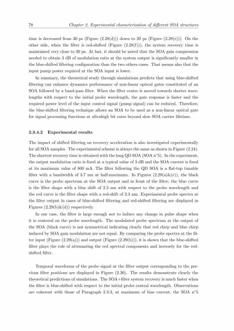
78 Chapter 2. Experimental characterisation of different SOA structures
time is decreased from 30 ps (Figure (2.28(d))) down to 20 ps (Figure (2.28(e))). On the
other side, when the filter is red-shifted (Figure (2.28(f))), the system recovery time is
maintained very close to 30 ps. At last, it should be noted that the SOA gain compression
needed to obtain 3 dB of modulation ratio at the system output is significantly smaller in
the blue-shifted filtering configuration than the two others cases. That means also that the
input pump power required at the SOA input is lower.
In summary, the theoretical study through simulations predicts that using blue-shifted
filtering can enhance dynamics performance of non-linear optical gates constituted of an
SOA followed by a band-pass filter. When the filter centre is moved towards shorter wave-
lengths with respect to the initial probe wavelength, the gate response is faster and the
required power level of the input control signal (pump signal) can be reduced. Therefore,
the blue-shifted filtering technique allows an SOA to be used as a non-linear optical gate
for signal processing functions at ultrahigh bit rates beyond slow SOA carrier lifetime.
2.3.4.2 Experimental results
The impact of shifted filtering on recovery acceleration is also investigated experimentally
for all SOA samples. The experimental scheme is always the same as shown in Figure (2.24).
The shortest recovery time is obtained with the long QD SOA (SOA n◦5). In the experiment,
the output modulation ratio is fixed at a typical value of 3 dB and the SOA current is fixed
at its maximum value of 800 mA. The filter following the QD SOA is a flat-top tunable
filter with a bandwidth of 3.7 nm at half-maximum. In Figures (2.29(a)&(c)), the black
curve is the probe spectrum at the SOA output and in front of the filter; the blue curve
is the filter shape with a blue shift of 2.3 nm with respect to the probe wavelength and
the red curve is the filter shape with a red-shift of 2.3 nm. Experimental probe spectra at
the filter output in cases of blue-shifted filtering and red-shifted filtering are displayed in
Figures (2.29(b)&(d)) respectively.
In our case, the filter is large enough not to induce any change in pulse shape when
it is centered on the probe wavelength. The modulated probe spectrum at the output of
the SOA (black curve) is not symmetrical indicating clearly that red chirp and blue chirp
induced by SOA gain modulation are not equal. By comparing the probe spectra at the fil-
ter input (Figure (2.29(a))) and output (Figure (2.29(b))), it is shown that the blue-shifted
filter plays the role of attenuating the red spectral components and inversely for the red-
shifted filter.
Temporal waveforms of the probe signal at the filter output corresponding to the pre-
vious filter positions are displayed in Figure (2.30). The results demonstrate clearly the
theoretical predictions of simulations. The SOA+filter system recovery is much faster when
the filter is blue-shifted with respect to the initial probe central wavelength. Observations
are coherent with those of Paragraph 2.3.3, at maximum of bias current, the SOA n◦5
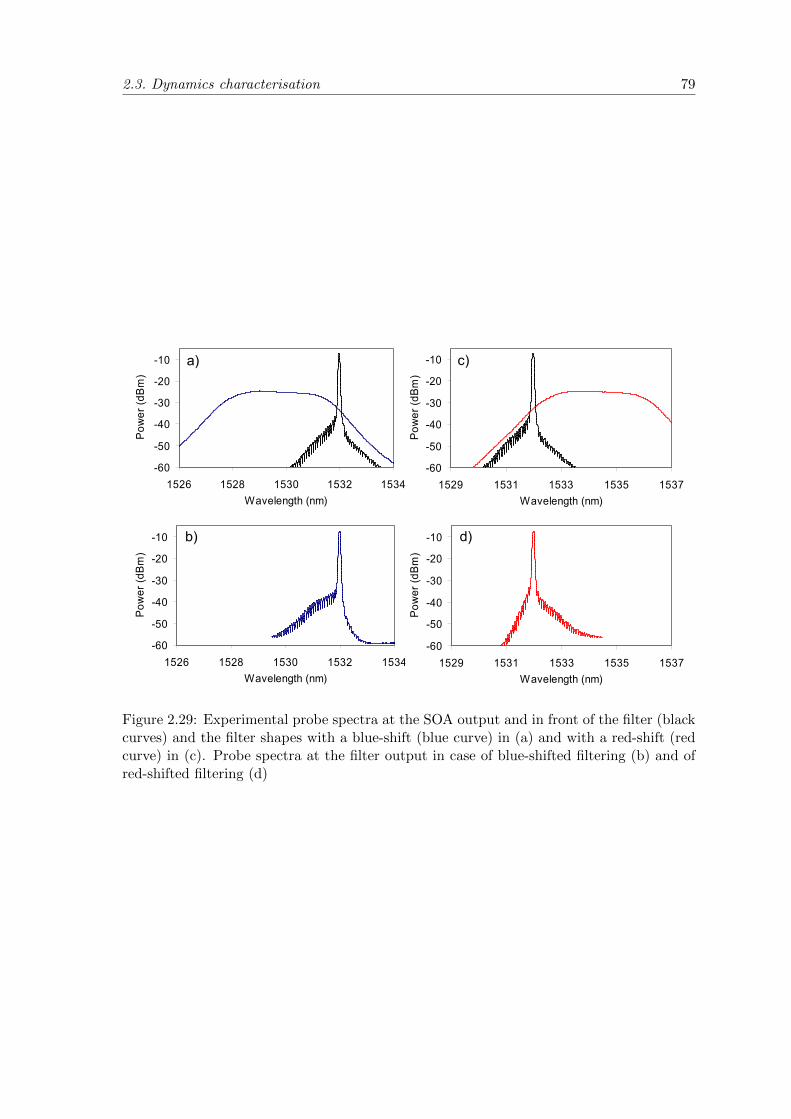
2.3. Dynamics characterisation 79
-60
-50
-40
-30
-20
-10
1526 1528 1530 1532 1534Wavelength (nm)
Pow
er (d
Bm
)
-60
-50
-40
-30
-20
-10
1526 1528 1530 1532 1534Wavelength (nm)
Pow
er (d
Bm
)
-60
-50
-40
-30
-20
-10
1529 1531 1533 1535 1537Wavelength (nm)
Pow
er (d
Bm)
-60
-50
-40
-30
-20
-10
1529 1531 1533 1535 1537Wavelength (nm)
Pow
er (d
Bm
)
a)
b)
c)
d)
-60
-50
-40
-30
-20
-10
1526 1528 1530 1532 1534Wavelength (nm)
Pow
er (d
Bm
)
-60
-50
-40
-30
-20
-10
1526 1528 1530 1532 1534Wavelength (nm)
Pow
er (d
Bm
)
-60
-50
-40
-30
-20
-10
1529 1531 1533 1535 1537Wavelength (nm)
Pow
er (d
Bm)
-60
-50
-40
-30
-20
-10
1529 1531 1533 1535 1537Wavelength (nm)
Pow
er (d
Bm
)
a)
b)
c)
d)
Figure 2.29: Experimental probe spectra at the SOA output and in front of the filter (blackcurves) and the filter shapes with a blue-shift (blue curve) in (a) and with a red-shift (redcurve) in (c). Probe spectra at the filter output in case of blue-shifted filtering (b) and ofred-shifted filtering (d)
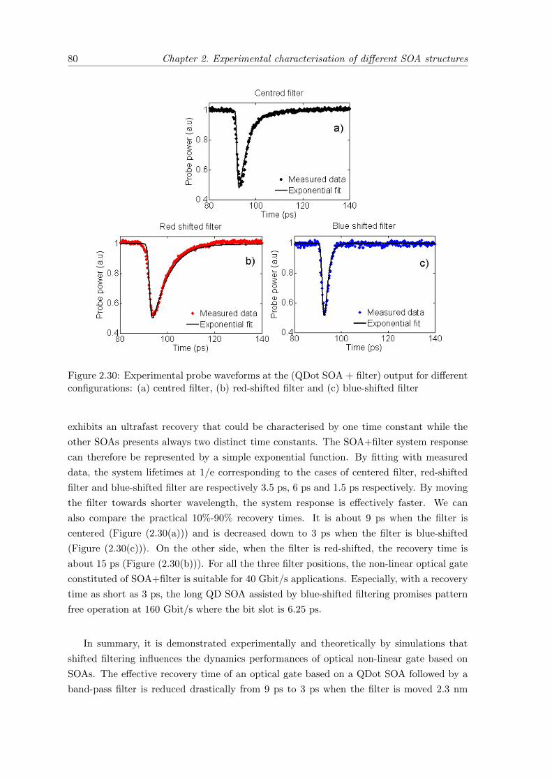
80 Chapter 2. Experimental characterisation of different SOA structures
Figure 2.30: Experimental probe waveforms at the (QDot SOA + filter) output for differentconfigurations: (a) centred filter, (b) red-shifted filter and (c) blue-shifted filter
exhibits an ultrafast recovery that could be characterised by one time constant while the
other SOAs presents always two distinct time constants. The SOA+filter system response
can therefore be represented by a simple exponential function. By fitting with measured
data, the system lifetimes at 1/e corresponding to the cases of centered filter, red-shifted
filter and blue-shifted filter are respectively 3.5 ps, 6 ps and 1.5 ps respectively. By moving
the filter towards shorter wavelength, the system response is effectively faster. We can
also compare the practical 10%-90% recovery times. It is about 9 ps when the filter is
centered (Figure (2.30(a))) and is decreased down to 3 ps when the filter is blue-shifted
(Figure (2.30(c))). On the other side, when the filter is red-shifted, the recovery time is
about 15 ps (Figure (2.30(b))). For all the three filter positions, the non-linear optical gate
constituted of SOA+filter is suitable for 40 Gbit/s applications. Especially, with a recovery
time as short as 3 ps, the long QD SOA assisted by blue-shifted filtering promises pattern
free operation at 160 Gbit/s where the bit slot is 6.25 ps.
In summary, it is demonstrated experimentally and theoretically by simulations that
shifted filtering influences the dynamics performances of optical non-linear gate based on
SOAs. The effective recovery time of an optical gate based on a QDot SOA followed by a
band-pass filter is reduced drastically from 9 ps to 3 ps when the filter is moved 2.3 nm
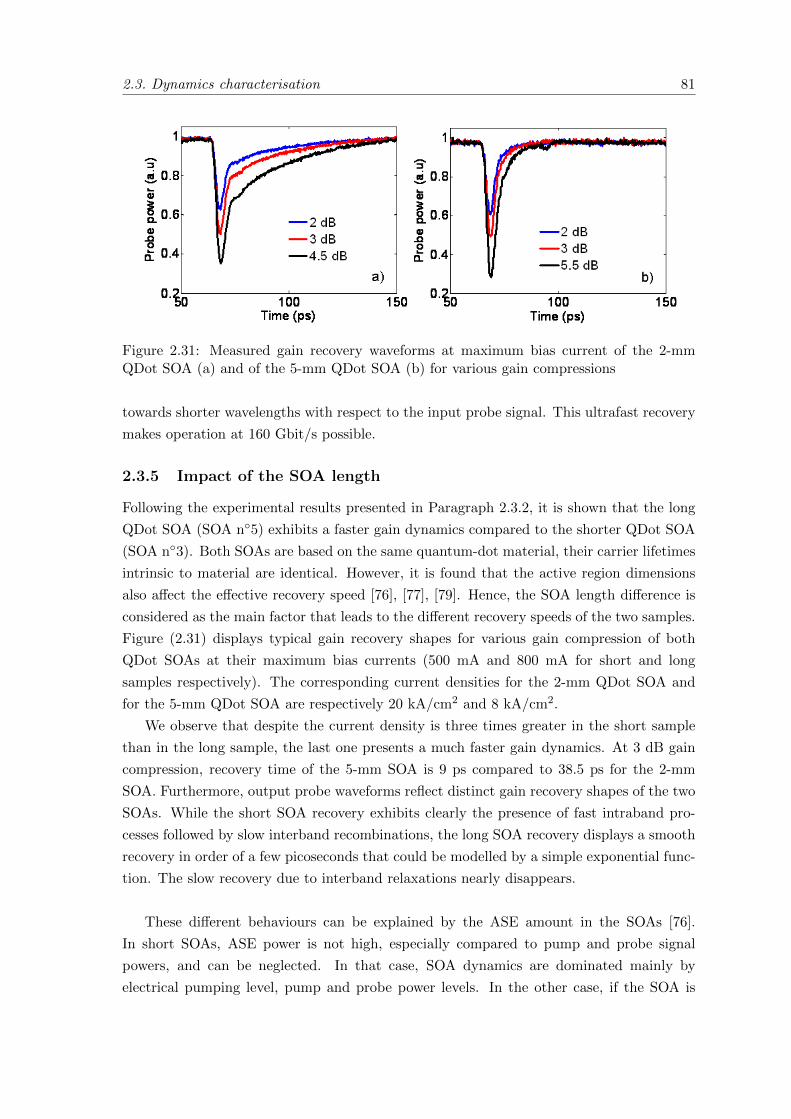
2.3. Dynamics characterisation 81
Figure 2.31: Measured gain recovery waveforms at maximum bias current of the 2-mmQDot SOA (a) and of the 5-mm QDot SOA (b) for various gain compressions
towards shorter wavelengths with respect to the input probe signal. This ultrafast recovery
makes operation at 160 Gbit/s possible.
2.3.5 Impact of the SOA length
Following the experimental results presented in Paragraph 2.3.2, it is shown that the long
QDot SOA (SOA n◦5) exhibits a faster gain dynamics compared to the shorter QDot SOA
(SOA n◦3). Both SOAs are based on the same quantum-dot material, their carrier lifetimes
intrinsic to material are identical. However, it is found that the active region dimensions
also affect the effective recovery speed [76], [77], [79]. Hence, the SOA length difference is
considered as the main factor that leads to the different recovery speeds of the two samples.
Figure (2.31) displays typical gain recovery shapes for various gain compression of both
QDot SOAs at their maximum bias currents (500 mA and 800 mA for short and long
samples respectively). The corresponding current densities for the 2-mm QDot SOA and
for the 5-mm QDot SOA are respectively 20 kA/cm2 and 8 kA/cm2.
We observe that despite the current density is three times greater in the short sample
than in the long sample, the last one presents a much faster gain dynamics. At 3 dB gain
compression, recovery time of the 5-mm SOA is 9 ps compared to 38.5 ps for the 2-mm
SOA. Furthermore, output probe waveforms reflect distinct gain recovery shapes of the two
SOAs. While the short SOA recovery exhibits clearly the presence of fast intraband pro-
cesses followed by slow interband recombinations, the long SOA recovery displays a smooth
recovery in order of a few picoseconds that could be modelled by a simple exponential func-
tion. The slow recovery due to interband relaxations nearly disappears.
These different behaviours can be explained by the ASE amount in the SOAs [76].
In short SOAs, ASE power is not high, especially compared to pump and probe signal
powers, and can be neglected. In that case, SOA dynamics are dominated mainly by
electrical pumping level, pump and probe power levels. In the other case, if the SOA is
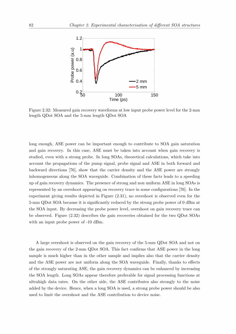
82 Chapter 2. Experimental characterisation of different SOA structures
50 100 1500.2
0.4
0.6
0.8
1
1.2
Time (ps)
Pro
be p
ower
(a.
u)
2 mm5 mm
Figure 2.32: Measured gain recovery waveforms at low input probe power level for the 2-mmlength QDot SOA and the 5-mm length QDot SOA
long enough, ASE power can be important enough to contribute to SOA gain saturation
and gain recovery. In this case, ASE must be taken into account when gain recovery is
studied, even with a strong probe. In long SOAs, theoretical calculations, which take into
account the propagations of the pump signal, probe signal and ASE in both forward and
backward directions [76], show that the carrier density and the ASE power are strongly
inhomogeneous along the SOA waveguide. Combination of these facts leads to a speeding
up of gain recovery dynamics. The presence of strong and non uniform ASE in long SOAs is
represented by an overshoot appearing on recovery trace in some configurations [76]. In the
experiment giving results depicted in Figure (2.31), no overshoot is observed even for the
5-mm QDot SOA because it is significantly reduced by the strong probe power of 0 dBm at
the SOA input. By decreasing the probe power level, overshoot on gain recovery trace can
be observed. Figure (2.32) describes the gain recoveries obtained for the two QDot SOAs
with an input probe power of -10 dBm.
A large overshoot is observed on the gain recovery of the 5-mm QDot SOA and not on
the gain recovery of the 2-mm QDot SOA. This fact confirms that ASE power in the long
sample is much higher than in the other sample and implies also that the carrier density
and the ASE power are not uniform along the SOA waveguide. Finally, thanks to effects
of the strongly saturating ASE, the gain recovery dynamics can be enhanced by increasing
the SOA length. Long SOAs appear therefore preferable for signal processing functions at
ultrahigh data rates. On the other side, the ASE contributes also strongly to the noise
added by the device. Hence, when a long SOA is used, a strong probe power should be also
used to limit the overshoot and the ASE contribution to device noise.
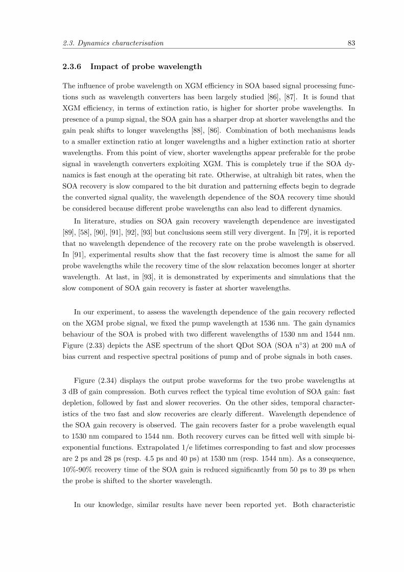
2.3. Dynamics characterisation 83
2.3.6 Impact of probe wavelength
The influence of probe wavelength on XGM efficiency in SOA based signal processing func-
tions such as wavelength converters has been largely studied [86], [87]. It is found that
XGM efficiency, in terms of extinction ratio, is higher for shorter probe wavelengths. In
presence of a pump signal, the SOA gain has a sharper drop at shorter wavelengths and the
gain peak shifts to longer wavelengths [88], [86]. Combination of both mechanisms leads
to a smaller extinction ratio at longer wavelengths and a higher extinction ratio at shorter
wavelengths. From this point of view, shorter wavelengths appear preferable for the probe
signal in wavelength converters exploiting XGM. This is completely true if the SOA dy-
namics is fast enough at the operating bit rate. Otherwise, at ultrahigh bit rates, when the
SOA recovery is slow compared to the bit duration and patterning effects begin to degrade
the converted signal quality, the wavelength dependence of the SOA recovery time should
be considered because different probe wavelengths can also lead to different dynamics.
In literature, studies on SOA gain recovery wavelength dependence are investigated
[89], [58], [90], [91], [92], [93] but conclusions seem still very divergent. In [79], it is reported
that no wavelength dependence of the recovery rate on the probe wavelength is observed.
In [91], experimental results show that the fast recovery time is almost the same for all
probe wavelengths while the recovery time of the slow relaxation becomes longer at shorter
wavelength. At last, in [93], it is demonstrated by experiments and simulations that the
slow component of SOA gain recovery is faster at shorter wavelengths.
In our experiment, to assess the wavelength dependence of the gain recovery reflected
on the XGM probe signal, we fixed the pump wavelength at 1536 nm. The gain dynamics
behaviour of the SOA is probed with two different wavelengths of 1530 nm and 1544 nm.
Figure (2.33) depicts the ASE spectrum of the short QDot SOA (SOA n◦3) at 200 mA of
bias current and respective spectral positions of pump and of probe signals in both cases.
Figure (2.34) displays the output probe waveforms for the two probe wavelengths at
3 dB of gain compression. Both curves reflect the typical time evolution of SOA gain: fast
depletion, followed by fast and slower recoveries. On the other sides, temporal character-
istics of the two fast and slow recoveries are clearly different. Wavelength dependence of
the SOA gain recovery is observed. The gain recovers faster for a probe wavelength equal
to 1530 nm compared to 1544 nm. Both recovery curves can be fitted well with simple bi-
exponential functions. Extrapolated 1/e lifetimes corresponding to fast and slow processes
are 2 ps and 28 ps (resp. 4.5 ps and 40 ps) at 1530 nm (resp. 1544 nm). As a consequence,
10%-90% recovery time of the SOA gain is reduced significantly from 50 ps to 39 ps when
the probe is shifted to the shorter wavelength.
In our knowledge, similar results have never been reported yet. Both characteristic
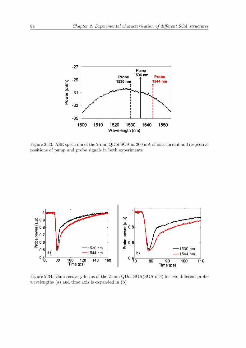
84 Chapter 2. Experimental characterisation of different SOA structures
-35
-33
-31
-29
-27
1500 1510 1520 1530 1540 1550Wavelength (nm)
Pow
er (d
Bm
)Pump
1536 nmProbe 1530 nm
Probe 1544 nm
-35
-33
-31
-29
-27
1500 1510 1520 1530 1540 1550Wavelength (nm)
Pow
er (d
Bm
)Pump
1536 nmProbe 1530 nm
Probe 1544 nm
Figure 2.33: ASE spectrum of the 2-mm QDot SOA at 200 mA of bias current and respectivepositions of pump and probe signals in both experiments
Figure 2.34: Gain recovery forms of the 2-mm QDot SOA(SOA n◦3) for two different probewavelengths (a) and time axis is expanded in (b)
2.3. Dynamics characterisation 85
times of the fast and slow recoveries are affected by the probe wavelength shift. Variations
of the fast and the slow recovery versus wavelength have never been observed simultane-
ously [89], [91], [93]. In [89], experimental results of a bulk InGaAsP based SOA showed a
greater recovery rate is obtained when the wavelength is moved from 1543 nm to 1533 nm.
Despite different time scales, we observe also a sharper fast recovery at 1530 nm compared
to 1544 nm. This wavelength dependence of the fast process can be explained as follows.
Contributions of different processes which are characterised by different time constants such
as SHB (hundreds of femtoseconds), CH (1 picosecond) and carrier density relaxation (hun-
dreds of picoseconds) to the global SOA gain dynamics vary also with the wavelength [58].
Theoretical predictions given by numerical simulations based on simplified density matrix
equations show good agreement between theory and experiment [89]. The measurements
were performed by using a degenerated pump-probe set-up with typical pulsewidth of 150 fs.
In another experiment [91] with similar pulse duration in order of 100 fs, but with a two
colour pump-probe technique (i.e pump and probe signals are at different wavelengths) ex-
perimental results disagree with the previous results. The authors observe no change in fast
recovery time for all probe wavelengths and the recovery time of the slower relaxation be-
comes longer for shorter wavelengths. This last observation is opposite to our results. The
authors explain longer recovery time by smaller saturation powers for shorter wavelengths
as shown in [88].
However, in the last experiments, the observation time is limited to only a few picosec-
onds and therefore does not allow the complete gain recovery dynamics to be observed.
Otherwise, in our experiment as well as in [93], the observation time scale is enlarged to
hundreds of picoseconds that allow the complete gain recovery to be assessed. In both
experiments, wavelength dependence tendencies of the slow recovery rate are consistent.
Recovery times of the slow recovery due to the interband relaxations appear shorter for
shorter wavelengths. This behaviour is indeed resulted from the fact that the SOA gain
spectrum is not symmetric with respect to the wavelength. During the band-to-band relax-
ation processes, the gain change at shorter wavelengths is larger than at longer wavelengths.
Consequently, the recovery speed is greater at shorter wavelengths.
At last, a relation between the gain recovery rate dependence on wavelength and the
wavelength dependence of the assessed SOA saturation power and of small-signal gain is
not evident. Static gain measurements of the SOA for signals at different wavelengths are
shown in Figure (2.35(a)). The small-signal gain changes are smaller than 1 dB and the
saturation powers are nearly the same for all signal wavelengths in the range from 1528 nm
to 1545 nm.
Gain recovery time is assessed via pump-probe measurements in XGM configuration for
two different wavelengths. The dynamic gain measurement was not performed exactly at
the probe wavelengths of 1528 nm and 1545 nm but it was performed at the very close
wavelengths of 1530 nm and 1544 nm respectively. Therefore, the static gain curves at
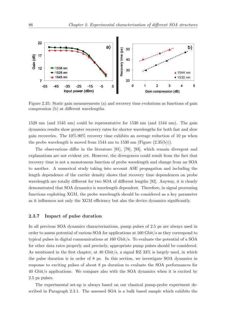
86 Chapter 2. Experimental characterisation of different SOA structures
20
30
40
50
0 1 2 3 4 5
Gain compression (dB)
Rec
over
y tim
e (p
s)
1544 nm1530 nm
7
12
17
22
-55 -45 -35 -25 -15 -5 5Input power (dBm)
Gai
n (d
B)
1538 nm1528 nm1545 nm
a) b)
20
30
40
50
0 1 2 3 4 5
Gain compression (dB)
Rec
over
y tim
e (p
s)
1544 nm1530 nm
7
12
17
22
-55 -45 -35 -25 -15 -5 5Input power (dBm)
Gai
n (d
B)
1538 nm1528 nm1545 nm
a) b)
Figure 2.35: Static gain measurements (a) and recovery time evolutions as functions of gaincompression (b) at different wavelengths
1528 nm (and 1545 nm) could be representative for 1530 nm (and 1544 nm). The gain
dynamics results show greater recovery rates for shorter wavelengths for both fast and slow
gain recoveries. The 10%-90% recovery time exhibits an average reduction of 10 ps when
the probe wavelength is moved from 1544 nm to 1530 nm (Figure (2.35(b))).
The observations differ in the literature [91], [79], [93], which remain divergent and
explanations are not evident yet. However, the divergences could result from the fact that
recovery time is not a monotonous function of probe wavelength and change from an SOA
to another. A numerical study taking into account ASE propagation and including the
length dependence of the carrier density shows that recovery time dependences on probe
wavelength are totally different for two SOA of different lengths [92]. Anyway, it is clearly
demonstrated that SOA dynamics is wavelength dependent. Therefore, in signal processing
functions exploiting XGM, the probe wavelength should be considered as a key parameter
as it influences not only the XGM efficiency but also the device dynamics significantly.
2.3.7 Impact of pulse duration
In all previous SOA dynamics characterisations, pump pulses of 2.5 ps are always used in
order to assess potential of various SOA for applications at 160 Gbit/s as they correspond to
typical pulses in digital communications at 160 Gbit/s. To evaluate the potential of a SOA
for other data rates properly and precisely, appropriate pump pulses should be considered.
As mentioned in the first chapter, at 40 Gbit/s, a signal RZ 33% is largely used, in which
the pulse duration is in order of 8 ps. In this section, we investigate SOA dynamics in
response to exciting pulses of about 8 ps duration to evaluate the SOA performances for
40 Gbit/s applications. We compare also with the SOA dynamics when it is excited by
2.5 ps pulses.
The experimental set-up is always based on our classical pump-probe experiment de-
scribed in Paragraph 2.3.1. The assessed SOA is a bulk based sample which exhibits the
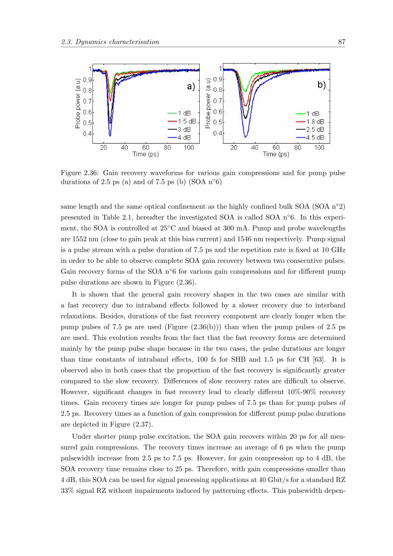
2.3. Dynamics characterisation 87
Figure 2.36: Gain recovery waveforms for various gain compressions and for pump pulsedurations of 2.5 ps (a) and of 7.5 ps (b) (SOA n◦6)
same length and the same optical confinement as the highly confined bulk SOA (SOA n◦2)
presented in Table 2.1, hereafter the investigated SOA is called SOA n◦6. In this experi-
ment, the SOA is controlled at 25◦C and biased at 300 mA. Pump and probe wavelengths
are 1552 nm (close to gain peak at this bias current) and 1546 nm respectively. Pump signal
is a pulse stream with a pulse duration of 7.5 ps and the repetition rate is fixed at 10 GHz
in order to be able to observe complete SOA gain recovery between two consecutive pulses.
Gain recovery forms of the SOA n◦6 for various gain compressions and for different pump
pulse durations are shown in Figure (2.36).
It is shown that the general gain recovery shapes in the two cases are similar with
a fast recovery due to intraband effects followed by a slower recovery due to interband
relaxations. Besides, durations of the fast recovery component are clearly longer when the
pump pulses of 7.5 ps are used (Figure (2.36(b))) than when the pump pulses of 2.5 ps
are used. This evolution results from the fact that the fast recovery forms are determined
mainly by the pump pulse shape because in the two cases, the pulse durations are longer
than time constants of intraband effects, 100 fs for SHB and 1.5 ps for CH [63]. It is
observed also in both cases that the proportion of the fast recovery is significantly greater
compared to the slow recovery. Differences of slow recovery rates are difficult to observe.
However, significant changes in fast recovery lead to clearly different 10%-90% recovery
times. Gain recovery times are longer for pump pulses of 7.5 ps than for pump pulses of
2.5 ps. Recovery times as a function of gain compression for different pump pulse durations
are depicted in Figure (2.37).
Under shorter pump pulse excitation, the SOA gain recovers within 20 ps for all mea-
sured gain compressions. The recovery times increase an average of 6 ps when the pump
pulsewidth increase from 2.5 ps to 7.5 ps. However, for gain compression up to 4 dB, the
SOA recovery time remains close to 25 ps. Therefore, with gain compressions smaller than
4 dB, this SOA can be used for signal processing applications at 40 Gbit/s for a standard RZ
33% signal RZ without impairments induced by patterning effects. This pulsewidth depen-
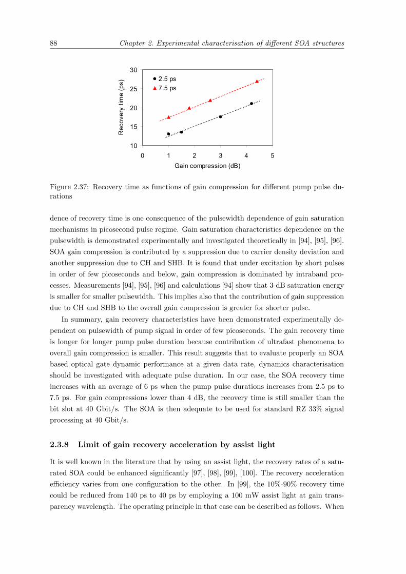
88 Chapter 2. Experimental characterisation of different SOA structures
10
15
20
25
30
0 1 2 3 4 5Gain compression (dB)
Rec
over
y tim
e (p
s) 2.5 ps7.5 ps
10
15
20
25
30
0 1 2 3 4 5Gain compression (dB)
Rec
over
y tim
e (p
s) 2.5 ps7.5 ps
Figure 2.37: Recovery time as functions of gain compression for different pump pulse du-rations
dence of recovery time is one consequence of the pulsewidth dependence of gain saturation
mechanisms in picosecond pulse regime. Gain saturation characteristics dependence on the
pulsewidth is demonstrated experimentally and investigated theoretically in [94], [95], [96].
SOA gain compression is contributed by a suppression due to carrier density deviation and
another suppression due to CH and SHB. It is found that under excitation by short pulses
in order of few picoseconds and below, gain compression is dominated by intraband pro-
cesses. Measurements [94], [95], [96] and calculations [94] show that 3-dB saturation energy
is smaller for smaller pulsewidth. This implies also that the contribution of gain suppression
due to CH and SHB to the overall gain compression is greater for shorter pulse.
In summary, gain recovery characteristics have been demonstrated experimentally de-
pendent on pulsewidth of pump signal in order of few picoseconds. The gain recovery time
is longer for longer pump pulse duration because contribution of ultrafast phenomena to
overall gain compression is smaller. This result suggests that to evaluate properly an SOA
based optical gate dynamic performance at a given data rate, dynamics characterisation
should be investigated with adequate pulse duration. In our case, the SOA recovery time
increases with an average of 6 ps when the pump pulse durations increases from 2.5 ps to
7.5 ps. For gain compressions lower than 4 dB, the recovery time is still smaller than the
bit slot at 40 Gbit/s. The SOA is then adequate to be used for standard RZ 33% signal
processing at 40 Gbit/s.
2.3.8 Limit of gain recovery acceleration by assist light
It is well known in the literature that by using an assist light, the recovery rates of a satu-
rated SOA could be enhanced significantly [97], [98], [99], [100]. The recovery acceleration
efficiency varies from one configuration to the other. In [99], the 10%-90% recovery time
could be reduced from 140 ps to 40 ps by employing a 100 mW assist light at gain trans-
parency wavelength. The operating principle in that case can be described as follows. When
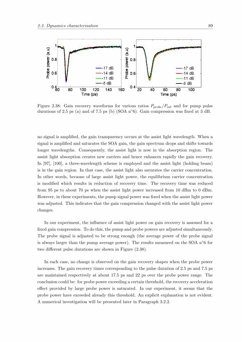
2.3. Dynamics characterisation 89
Figure 2.38: Gain recovery waveforms for various ratios Pprobe/Psat and for pump pulsedurations of 2.5 ps (a) and of 7.5 ps (b) (SOA n◦6). Gain compression was fixed at 3 dB.
no signal is amplified, the gain transparency occurs at the assist light wavelength. When a
signal is amplified and saturates the SOA gain, the gain spectrum drops and shifts towards
longer wavelengths. Consequently, the assist light is now in the absorption region. The
assist light absorption creates new carriers and hence enhances rapidly the gain recovery.
In [97], [100], a three-wavelength scheme is employed and the assist light (holding beam)
is in the gain region. In that case, the assist light also saturates the carrier concentration.
In other words, because of large assist light power, the equilibrium carrier concentration
is modified which results in reduction of recovery time. The recovery time was reduced
from 95 ps to about 70 ps when the assist light power increased from 10 dBm to 0 dBm.
However, in these experiments, the pump signal power was fixed when the assist light power
was adjusted. This indicates that the gain compression changed with the assist light power
changes.
In our experiment, the influence of assist light power on gain recovery is assessed for a
fixed gain compression. To do this, the pump and probe powers are adjusted simultaneously.
The probe signal is adjusted to be strong enough (the average power of the probe signal
is always larger than the pump average power). The results measured on the SOA n◦6 for
two different pulse durations are shown in Figure (2.38).
In each case, no change is observed on the gain recovery shapes when the probe power
increases. The gain recovery times corresponding to the pulse duration of 2.5 ps and 7.5 ps
are maintained respectively at about 17.5 ps and 22 ps over the probe power range. The
conclusion could be: for probe power exceeding a certain threshold, the recovery acceleration
effect provided by large probe power is saturated. In our experiment, it seems that the
probe power have exceeded already this threshold. An explicit explanation is not evident.
A numerical investigation will be presented later in Paragraph 3.2.2.
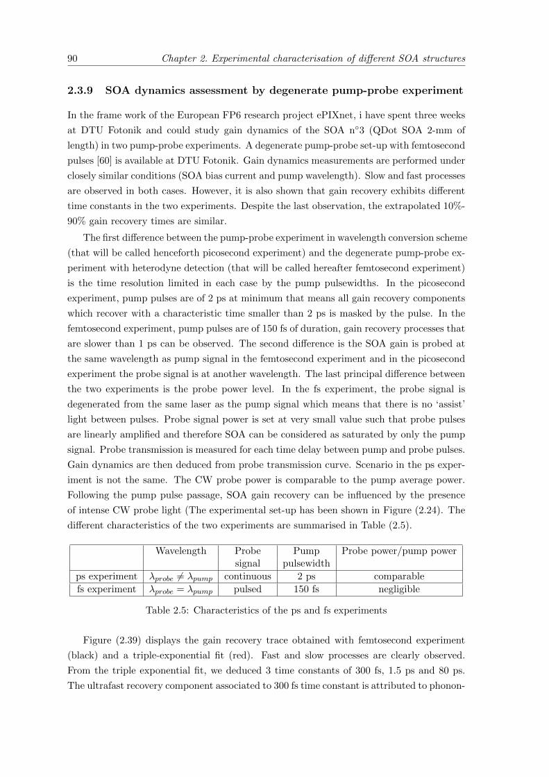
90 Chapter 2. Experimental characterisation of different SOA structures
2.3.9 SOA dynamics assessment by degenerate pump-probe experiment
In the frame work of the European FP6 research project ePIXnet, i have spent three weeks
at DTU Fotonik and could study gain dynamics of the SOA n◦3 (QDot SOA 2-mm of
length) in two pump-probe experiments. A degenerate pump-probe set-up with femtosecond
pulses [60] is available at DTU Fotonik. Gain dynamics measurements are performed under
closely similar conditions (SOA bias current and pump wavelength). Slow and fast processes
are observed in both cases. However, it is also shown that gain recovery exhibits different
time constants in the two experiments. Despite the last observation, the extrapolated 10%-
90% gain recovery times are similar.
The first difference between the pump-probe experiment in wavelength conversion scheme
(that will be called henceforth picosecond experiment) and the degenerate pump-probe ex-
periment with heterodyne detection (that will be called hereafter femtosecond experiment)
is the time resolution limited in each case by the pump pulsewidths. In the picosecond
experiment, pump pulses are of 2 ps at minimum that means all gain recovery components
which recover with a characteristic time smaller than 2 ps is masked by the pulse. In the
femtosecond experiment, pump pulses are of 150 fs of duration, gain recovery processes that
are slower than 1 ps can be observed. The second difference is the SOA gain is probed at
the same wavelength as pump signal in the femtosecond experiment and in the picosecond
experiment the probe signal is at another wavelength. The last principal difference between
the two experiments is the probe power level. In the fs experiment, the probe signal is
degenerated from the same laser as the pump signal which means that there is no ‘assist’
light between pulses. Probe signal power is set at very small value such that probe pulses
are linearly amplified and therefore SOA can be considered as saturated by only the pump
signal. Probe transmission is measured for each time delay between pump and probe pulses.
Gain dynamics are then deduced from probe transmission curve. Scenario in the ps exper-
iment is not the same. The CW probe power is comparable to the pump average power.
Following the pump pulse passage, SOA gain recovery can be influenced by the presence
of intense CW probe light (The experimental set-up has been shown in Figure (2.24). The
different characteristics of the two experiments are summarised in Table (2.5).
Wavelength Probe Pump Probe power/pump powersignal pulsewidth
ps experiment λprobe 6= λpump continuous 2 ps comparable
fs experiment λprobe = λpump pulsed 150 fs negligible
Table 2.5: Characteristics of the ps and fs experiments
Figure (2.39) displays the gain recovery trace obtained with femtosecond experiment
(black) and a triple-exponential fit (red). Fast and slow processes are clearly observed.
From the triple exponential fit, we deduced 3 time constants of 300 fs, 1.5 ps and 80 ps.
The ultrafast recovery component associated to 300 fs time constant is attributed to phonon-
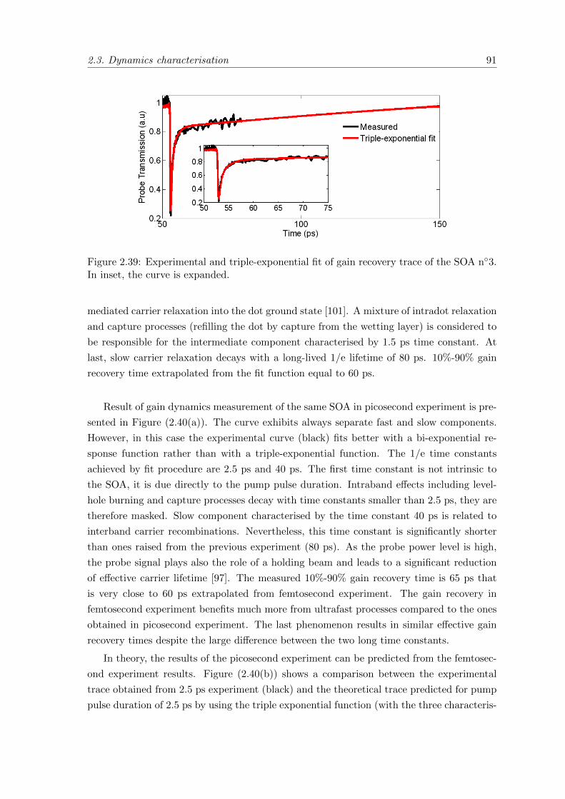
2.3. Dynamics characterisation 91
Figure 2.39: Experimental and triple-exponential fit of gain recovery trace of the SOA n◦3.In inset, the curve is expanded.
mediated carrier relaxation into the dot ground state [101]. A mixture of intradot relaxation
and capture processes (refilling the dot by capture from the wetting layer) is considered to
be responsible for the intermediate component characterised by 1.5 ps time constant. At
last, slow carrier relaxation decays with a long-lived 1/e lifetime of 80 ps. 10%-90% gain
recovery time extrapolated from the fit function equal to 60 ps.
Result of gain dynamics measurement of the same SOA in picosecond experiment is pre-
sented in Figure (2.40(a)). The curve exhibits always separate fast and slow components.
However, in this case the experimental curve (black) fits better with a bi-exponential re-
sponse function rather than with a triple-exponential function. The 1/e time constants
achieved by fit procedure are 2.5 ps and 40 ps. The first time constant is not intrinsic to
the SOA, it is due directly to the pump pulse duration. Intraband effects including level-
hole burning and capture processes decay with time constants smaller than 2.5 ps, they are
therefore masked. Slow component characterised by the time constant 40 ps is related to
interband carrier recombinations. Nevertheless, this time constant is significantly shorter
than ones raised from the previous experiment (80 ps). As the probe power level is high,
the probe signal plays also the role of a holding beam and leads to a significant reduction
of effective carrier lifetime [97]. The measured 10%-90% gain recovery time is 65 ps that
is very close to 60 ps extrapolated from femtosecond experiment. The gain recovery in
femtosecond experiment benefits much more from ultrafast processes compared to the ones
obtained in picosecond experiment. The last phenomenon results in similar effective gain
recovery times despite the large difference between the two long time constants.
In theory, the results of the picosecond experiment can be predicted from the femtosec-
ond experiment results. Figure (2.40(b)) shows a comparison between the experimental
trace obtained from 2.5 ps experiment (black) and the theoretical trace predicted for pump
pulse duration of 2.5 ps by using the triple exponential function (with the three characteris-
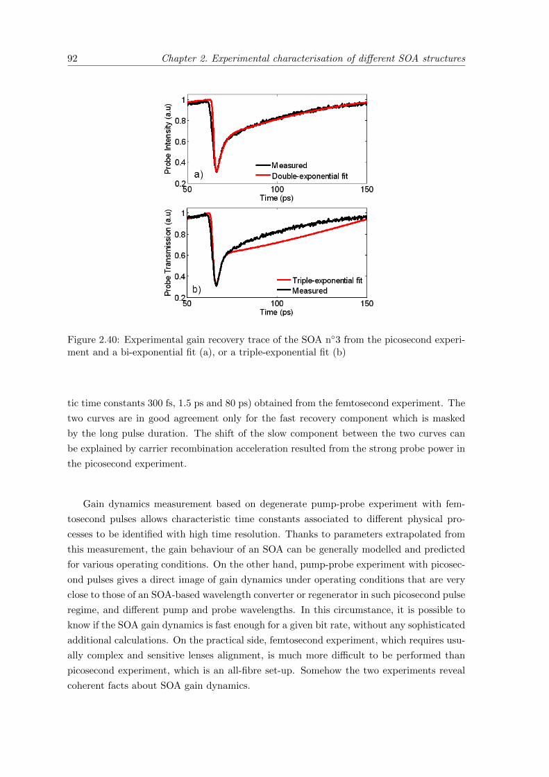
92 Chapter 2. Experimental characterisation of different SOA structures
Figure 2.40: Experimental gain recovery trace of the SOA n◦3 from the picosecond experi-ment and a bi-exponential fit (a), or a triple-exponential fit (b)
tic time constants 300 fs, 1.5 ps and 80 ps) obtained from the femtosecond experiment. The
two curves are in good agreement only for the fast recovery component which is masked
by the long pulse duration. The shift of the slow component between the two curves can
be explained by carrier recombination acceleration resulted from the strong probe power in
the picosecond experiment.
Gain dynamics measurement based on degenerate pump-probe experiment with fem-
tosecond pulses allows characteristic time constants associated to different physical pro-
cesses to be identified with high time resolution. Thanks to parameters extrapolated from
this measurement, the gain behaviour of an SOA can be generally modelled and predicted
for various operating conditions. On the other hand, pump-probe experiment with picosec-
ond pulses gives a direct image of gain dynamics under operating conditions that are very
close to those of an SOA-based wavelength converter or regenerator in such picosecond pulse
regime, and different pump and probe wavelengths. In this circumstance, it is possible to
know if the SOA gain dynamics is fast enough for a given bit rate, without any sophisticated
additional calculations. On the practical side, femtosecond experiment, which requires usu-
ally complex and sensitive lenses alignment, is much more difficult to be performed than
picosecond experiment, which is an all-fibre set-up. Somehow the two experiments reveal
coherent facts about SOA gain dynamics.
2.3. Dynamics characterisation 93
- 2 0 2 4 6 8 1 0
- 5 0
0
5 0
1 0 0
D e l a y ( p s )
40 mA
150 mA
Pha
se (
deg)
Delay (ps)-2 0 2 4 6 8 10
Pha
se (d
eg)
100
50
0
-50- 2 0 2 4 6 8 1 0
- 5 0
0
5 0
1 0 0
D e l a y ( p s )
40 mA
150 mA
Pha
se (
deg)
Delay (ps)-2 0 2 4 6 8 10- 2 0 2 4 6 8 1 0
- 5 0
0
5 0
1 0 0
D e l a y ( p s )
40 mA
150 mA
Pha
se (
deg)
- 2 0 2 4 6 8 1 0
- 5 0
0
5 0
1 0 0
D e l a y ( p s )
40 mA
150 mA
Pha
se (
deg)
Delay (ps)-2 0 2 4 6 8 10
Pha
se (d
eg)
100
50
0
-50
Figure 2.41: Experimental phase recovery of the 2-mm length QDot SOA for different biascurrents (measurements of Per Lunnemann and Sara Ek of DTU Fotonik)
2.3.10 Phase dynamics
All-optical signal processing devices based on interferometer configurations rely not only
on XGM but also on XPM in SOAs. Using such a device requires therefore information
about both SOA gain and phase dynamics. A gain modulation is always accompanied
by a refractive index modulation because both depend on the carrier density. And the
refractive index modulation results in time dependent phase shift on the signals travelling
through the SOA. Phase dynamics measurements were also performed in the same frame
work of cooperation with DTU Fotonik. Thanks to degenerate pump-probe set-up with
heterodyne detection, phase changes due to refractive index modulation in the SOA could
be measured. The SOA under investigation is always the 2-mm length QDot SOA (SOA
n◦3). Experimental results are presented in Figure (2.41). Measurements are performed by
Per Lunnemann and Sara Ek, PhD students at DTU Fotonik.
The optical signal wavelength is 1550 nm, pump pulse energy is estimated about 1 pJ at
the SOA input. Phase dynamics is measured at two bias currents of 40 mA and of 150 mA.
At 40 mA, close to the transparency current for 1550 nm, no significant phase change is
observed because the pump pulse is simply transmitted and there is nearly no carrier density
modulation due to optical pulse presence. At 150 mA, well above the SOA threshold current,
phase shifts induced by optical pulse presence are observed. The phase recovery curve is
consistent with other experimental results reported in the literature [102], [103], [72]. An
instantaneous negative phase shift is observed first which is assigned to the instantaneous
Two Photon Absorption (TPA) effect and the Level Hole Burning in the dots. This is
followed by a large positive phase shift distributed by both CH and carrier depletion. At
last, the phase shift recovers slowly. The gain, as presented previously in Paragraph 2.3.9,
recovers by two distinguished steps characterised by two different time constants. On the
contrary, the phase dynamics exhibits a monotonous recovery which can be characterised by
94 Chapter 2. Experimental characterisation of different SOA structures
only one time constant. The phase recovery trace is measured within only few picoseconds,
it is difficult to extrapolate precisely this decade time constant. However, a time constant
in order of 40-100 ps seems reasonable. This long lifetime suggests that phase change is
dominated by the slow processes of long lived carrier relaxations in opposition to the gain
compression which is dominated rather by fast intradot processes.
These distinguished behaviours of gain and phase dynamics induced by carrier modu-
lation originate from different linewidth enhancement factors (Henry factor) associated to
slow and fast processes. Phase changes could be deduced from gain compression via the
proportional factors alpha [61]. Despite the large distribution of gain suppression due to
fast processes to the over all gain compression, the alpha factor associated to these fast
processes CH and SHB is much smaller than the one associated to the carrier depletion
and consequently the total phase shift is attributed mostly to the last one. Hence, phase
changes recover with the slow carrier relaxations and is characterised by the corresponding
long lived time constant.
In summary, it is experimentally demonstrated that SOA gain and phase dynamics
exhibit dissimilar behaviours. Gain dynamics is dominated by intraband processes and
recovers with the corresponding short time constant. On the contrary, phase dynamics is
distributed mostly by the carrier depletion and hence recovers with the corresponding long
time constant. Signal processing schemes exploiting XGM could take profits from this fast
gain dynamics. Design of signal processing devices exploiting XPM has to take into account
carefully the slow recovery of phase. And finally, devices based on differential interferometer
configurations have to consider simultaneously the SOA gain and phase dynamics as in such
schemes both XGM and XPM are involved in the signal processing.
2.4. Chapter summary 95
2.4 Chapter summary
In this chapter, experimental characterisations of all investigated SOAs were presented.
These SOAs are designed for applications in all-optical signal processing functions such as
regeneration and wavelength conversion, at 40 Gbit/s and up to 160 Gbit/s. Some basic
descriptions of SOA were reminded first. Qualitative description of the two main features:
gain saturation and SOA dynamics was also discussed.
The second section was dedicated to present results of static characterisations. First of
all, two coupling beds were presented. Using of micro-lensed fibres allows a flexible and all-
fibred characterisation bed adapted for any SOA chip. With a wide range of optical mode
diameter offered by micro-lensed fibres, one-side loss of fibre-chip coupling is typically only
2 dB. SOA module using lenses offers also a low-loss fibre-chip coupling could be as small as
1.5 dB with high stability and robustness. This module coupling efficiency is much greater
than the commercially available butterfly package. Signal processing applications require
firstly high small-signal gain, small saturation power and no ripple. Static characterisations
provide this primary and fundamental information. Among the investigated SOAs, the bulk
based ones exhibit small-signal chip gains as high as 30 dB with 3-dB saturation powers
as low as 27 dBm, the quantum material based SOAs exhibit small-signal chip gains of at
least 20 dB and 3-dB saturation powers smaller than 16 dBm. Except the ultralong QDot
SOA (5-mm length QDot SOA), others SOAs expose small ripple down to 0.5 dB (tech-
nology limitation). These SOAs fulfil primary conditions for all-optical signal processing
applications.
The third section is devoted entirely to experimental characterisations of SOA dynamics.
Fast response is the key feature of SOA based signal processing functions for operating at
ultrahigh bit rates of 40 Gbit/s and up to 160 Gbit/s. Pump-probe experiment based
on XGM in SOA is elaborated. With pump pulse durations variable and in order of few
picoseconds, this pump-probe set-up allows to assess SOA gain dynamics behaviour under
conditions which is closed to real operating conditions in a regenerator or a wavelength
converter at these data rates. Moreover, the tunability of pump and probe wavelengths
on the whole C-band is also an advantage of the set-up. The first question when the bit
rate increase is the device response speed. It is shown that the effective SOA gain recovery
time depend on gain compression. Despite the presence of the long carrier relaxations
in order of 100 ps, SOA can operate at 40 Gbit/s without significant patterning effects
if the gain compression is small enough. This could be possible thanks to the fact that
under saturation induced by picosecond pulses, the gain compression takes advantages from
ultrafast intraband effects such as CH and SHB and hence recovers a great part with short
characteristic time associated to these effects. It is also demonstrated that by increasing the
bias current, SOA response time could be shortened significantly. The gain recovery time of
96 Chapter 2. Experimental characterisation of different SOA structures
the long QDot SOA is decreased drastically from an average of 30 ps to 10 ps when its bias
current is raised from 300 mA to its maximal value of 800 mA. Although, a gain recovery
time of 10 ps is not small enough for an operation at 160 Gbit/s at which the bit slot is only
about 6 ps. To attain the bit rate of 160 Gbit/s and beyond, shifted filtering appears as the
simplest solution to enhance the dynamics of SOA based non-linear optical gate. Impact
of position of the filter following the SOA was assessed. Results show that a red-shifted
filtering does not allow to enhance the dynamics of the SOA based non-linear optical gate.
On the other side, it is clearly demonstrated that a blue-shifted filtering improves efficiently
the gain compression time response compromise of the gate. By placing a blue-shifted filter
followed the long QDot SOA, a recovery time of 3 ps was obtained for a gain compression
of 3 dB. This ultrafast response of the optical gate promises an operation at 160 Gbit/s
without any patterning effects. Impact of probe wavelength on SOA based optical gate was
also studied. Results show that recovery time could be smaller for shorter probe wavelength.
However, the conclusion about probe wavelength influence is still divergent. This last can
originate from gain spectra that could be very different from one to other SOA. It is shown
also that SOA recovery time is longer for longer pump pulse duration. Because the pulse
duration varies generally with the bit rate, to evaluate properly the performance of the SOA
based non-linear gate performance for a precise data rate, adequate pulse duration should
be considered in dynamics characterisations.
Dynamics characterisation of various SOA structures reveals also influences of waveguide
design on SOA dynamics performance. A highly confined SOA will be preferable because
a greater collection of injected signal into the SOA active region waveguide could result
in a shorter effective recovery time. Especially, by increasing the chip length, SOA gain
dynamics becomes faster thanks to the distribution of strong ASE to gain saturation and
therefore to gain recovery. Finally, quantum-dot material based SOAs affirm their advan-
tages for all-optical signal processing at ultrahigh bit rates. Despite the very small-optical
confinement ( 1%) QDot SOAs exhibit a fast dynamics comparable to highly confined bulk
based SOA. The shortest recovery time of 3 ps is obtained by associating the long QDot
SOA with a blue-shifted filtering which promises a pattern free operation at 160 Gbit/s.
At last, SOA dynamics was performed with high temporal resolution in a degenerate
pump-probe experiment using 150 fs pulses for the 2-mm length QDot SOA. Gain dynam-
ics results reveals coherent physical facts with those obtained in our wavelength conversion
based pump-probe experiment. Attention must be paid on phase dynamics results. Phase
recovery is dominated by slow processes, on the contrary with gain recovery that is domi-
nated rather by fast processes. This fact is imputed to the weak coupling between the gain
compression due to intraband processes and the corresponding induced phase modulation.
Most of SOA based all-optical signal processing devices rely on the XGM and XPM pro-
cesses. Understanding of SOAs’ gain and phase with reliable experimental information is a
key issue to obtain optimal operating performance of SOA based non-linear optical gates.
Chapter 3
Numerical study of SOA dynamics
According to the experimental results of the SOA dynamics measurements presented in
Chapter 2, the gain compression is not only contributed by a component related to interband
processes but also by another component related to intraband processes. Consequently, the
gain recovery exhibits an ultrafast relaxation, characterised by a time constant in order of
few picoseconds, and a slow relaxation, characterised by a time constant in order of 100 ps.
The fast gain recovery reveals the presence of the intraband relaxations such as Carrier
Heating (CH) and Spectral Hole Burning (SHB) and the slow recovery reveals the presence
of carrier interband relaxations. The effect of intraband dynamics becomes more important
when the pulse width becomes smaller. Otherwise, when the pulsewidth is in order of
few picoseconds (corresponding to the data rates such as 40 Gbit/s and 160 Gbit/s), the
intraband dynamics has to be considered in SOA dynamics investigations. On one hand, to
understand the influences of these ultrafast processes on the gain dynamics, it is necessary
to develop an SOA model including the intraband phenomena. Consequently, their impact
on the performance of the SOA non-linear gates could be examined. On the other hand,
the model must be simple enough to be introduced easily in different regenerator schemes
in order to avoid cumbersome system simulations. In this context, the model which was
proposed by [14] concerning the injection laser relaxation and was adapted for the injection
SOA recovery by [15] appears quite adequate. In the first section, the main backgrounds
on the SOA model are presented. The results of the numerical study on the SOA dynamics
are then reported in Section 3.2 and summarised in Section 3.3.
3.1 SOA model
Some hypotheses of SOA intrinsic characteristics have to be considered. The studied SOA
has to be a travelling-wave amplifier and the waveguide dimensions are such that the am-
plifier supports only one guided mode. It is usually the case in practice. The studied SOA
structures have the thickness and the width in order of 1 µm and the length in order from
1 mm to few millimetres. The width and the thickness of these active regions are smaller
98 Chapter 3. Numerical study of SOA dynamics
than the scattering length whereas the length is much larger. The last hypothesis allows
the carrier density to be considered as nearly uniform along the transverse dimensions and
the carrier scattering can be neglected. Another assumption which is currently taken into
account to simplify the propagation equation is that the amplifier intrinsic losses: they are
considered negligible compared to the accumulated gain during pulse propagation. An as-
sumption of operating conditions should be also respected. The model is valid for injection
pulse durations exceeding 1 ps. This condition implies that the spectral width of pulses is
sufficiently small compared to the SOA gain bandwidth and therefore the spectral effects
could be neglected. This assumption enables the considerable simplification of density ma-
trix formulation as proposed in [14]. In the gain dynamics experiment presented in Section
2.3, the pump pulse duration is typically 2.5 ps. Then, this SOA model could be used to
simulate the gain dynamics measured in the experiment. For further studies involving SOA
insertion into system simulations, the pulse duration at the considered data rates (40 Gbit/s
and 160 Gbit/s) exceeds always 1 ps and thus this SOA model will still be suitable.
Indeed, the carrier population is divided into two parts, with N1 and N2 carriers re-
spectively. N1 represents the number of carriers which directly contribute to the SOA gain.
That means their energies are close to the photon energy of the injected optical signal. N2
corresponds to all the other carriers. Their energies are out of the band involved in the
stimulated emission process. The carriers of these two populations are redistributed by
intraband relaxations. The distribution of the final state is assumed to be the distribution
at the thermal equilibrium. The rate equations associated to the two population evolutions
can be written as Equations (3-1) and (3-2) [15]:
∂N1
∂t=IU
q− PN1
Es− N1
τs− ∆N
τc(3-1)
∂N2
∂t=I (1− U)
q− N2
τs+
∆N
τc(3-2)
with:
U =λ2
πc× 1
τc∆λ(3-3)
∆N = N1 (1− U)−N2U (3-4)
Ns = N1 +N2 (3-5)
Es =hυσma
(3-6)
g =Γa
VN1 (3-7)
where:
c = 3× 10⁸m/s is the velocity of light in vacuum,
q = 1.6× 10⁻¹⁹C is the electron charge,
h = 6.625× 10⁻³⁴J.s is the Planck constant,
3.1. SOA model 99
I is the injection current,
λ is the signal wavelength,
ν is the signal frequency,
∆λ is the half width of the SOA spontaneous emission spectrum,
V is the active volume,
σm is the mode cross section,
γ is the confinement factor,
a is the gain coefficient,
Es is the saturation energy if the amplifier,
τs is the interband life-time,
τc is the intraband life-time,
Ns is the total carrier population,
∆N is the deviation from thermal equilibrium due to optical pulses,
P is the optical power.
The propagation of the electromagnetic field inside the SOA is governed by the following
Equation (3-8):∂A
∂z+
1
vg× ∂A
∂t=
1
2(1 + iα) gA (3-8)
A (z, t) is the slowly varying envelope associated with the optical pulse. vg is the group
velocity. α is the linewidth enhancement factor.
Equations (3-1), (3-2) and (3-8) can be simplified by applying the transformation:
τ = t− z
vg(3-9)
It is also useful to separate the amplitude and the phase of the pulse by writing:
A =√P exp (iφ) (3-10)
with P (z, τ) is the power and φ (z, τ) is the phase. Consequently, Equation (3-8) is
equivalent to the following set of two Equations (3-11) and (3-16):
∂P
∂z= gP (3-11)
∂φ
∂z= −1
2αg (3-12)
By using Equations (3-1), (3-2) and (3-4), ∆N and N2 can be eliminated to obtain one
rate equation of the only unknown N1. By taking into account that τc << τs, the rate
equation that governs the N1 evolution can be expressed as Equation (3-13):
∂2N1
∂τ2+
1
τc× ∂N1
∂t=IU
qτc− N1
τsτc−(
U
Esτc+
1
Esτs
)PN1 −
1
Es× ∂ (PN1)
∂τ(3-13)
100 Chapter 3. Numerical study of SOA dynamics
If we define the function h (τ) which physically represents the accumulated gain at each
point of the pulse profile, by Equation (3-14):
h (τ) =
L∫0
gdz (3-14)
and integrate Equation (3-13) over the amplifier length and Equations (3-7) and (3-11)
together then lead to Equation (3-15):
d2h
dτ2+
1
τc×dhdτ
=IUΓaL
qV τc− h
τsτc−(
U
ESτc+
1
Esτs
)[exp (h)− 1]P (τ, 0)− 1
Es× d
dτ{[exp (h)− 1]P (τ, 0)}
(3-15)
Equation (3-15) could be solved numerically to obtain h (τ). All details of the interme-
diate calculations are reported in Appendix 1.
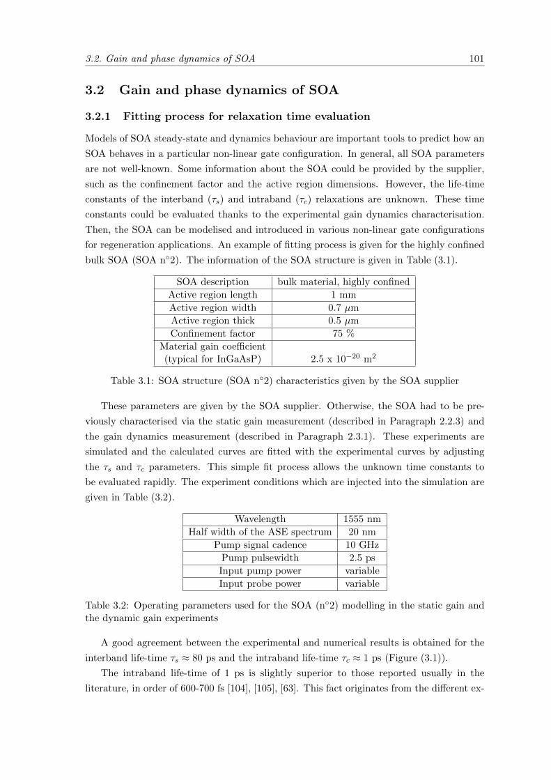
3.2. Gain and phase dynamics of SOA 101
3.2 Gain and phase dynamics of SOA
3.2.1 Fitting process for relaxation time evaluation
Models of SOA steady-state and dynamics behaviour are important tools to predict how an
SOA behaves in a particular non-linear gate configuration. In general, all SOA parameters
are not well-known. Some information about the SOA could be provided by the supplier,
such as the confinement factor and the active region dimensions. However, the life-time
constants of the interband (τs) and intraband (τc) relaxations are unknown. These time
constants could be evaluated thanks to the experimental gain dynamics characterisation.
Then, the SOA can be modelised and introduced in various non-linear gate configurations
for regeneration applications. An example of fitting process is given for the highly confined
bulk SOA (SOA n◦2). The information of the SOA structure is given in Table (3.1).
SOA description bulk material, highly confined
Active region length 1 mm
Active region width 0.7 µm
Active region thick 0.5 µm
Confinement factor 75 %
Material gain coefficient(typical for InGaAsP) 2.5 x 10⁻²⁰ m2
Table 3.1: SOA structure (SOA n◦2) characteristics given by the SOA supplier
These parameters are given by the SOA supplier. Otherwise, the SOA had to be pre-
viously characterised via the static gain measurement (described in Paragraph 2.2.3) and
the gain dynamics measurement (described in Paragraph 2.3.1). These experiments are
simulated and the calculated curves are fitted with the experimental curves by adjusting
the τs and τc parameters. This simple fit process allows the unknown time constants to
be evaluated rapidly. The experiment conditions which are injected into the simulation are
given in Table (3.2).
Wavelength 1555 nm
Half width of the ASE spectrum 20 nm
Pump signal cadence 10 GHz
Pump pulsewidth 2.5 ps
Input pump power variable
Input probe power variable
Table 3.2: Operating parameters used for the SOA (n◦2) modelling in the static gain andthe dynamic gain experiments
A good agreement between the experimental and numerical results is obtained for the
interband life-time τs ≈ 80 ps and the intraband life-time τc ≈ 1 ps (Figure (3.1)).
The intraband life-time of 1 ps is slightly superior to those reported usually in the
literature, in order of 600-700 fs [104], [105], [63]. This fact originates from the different ex-
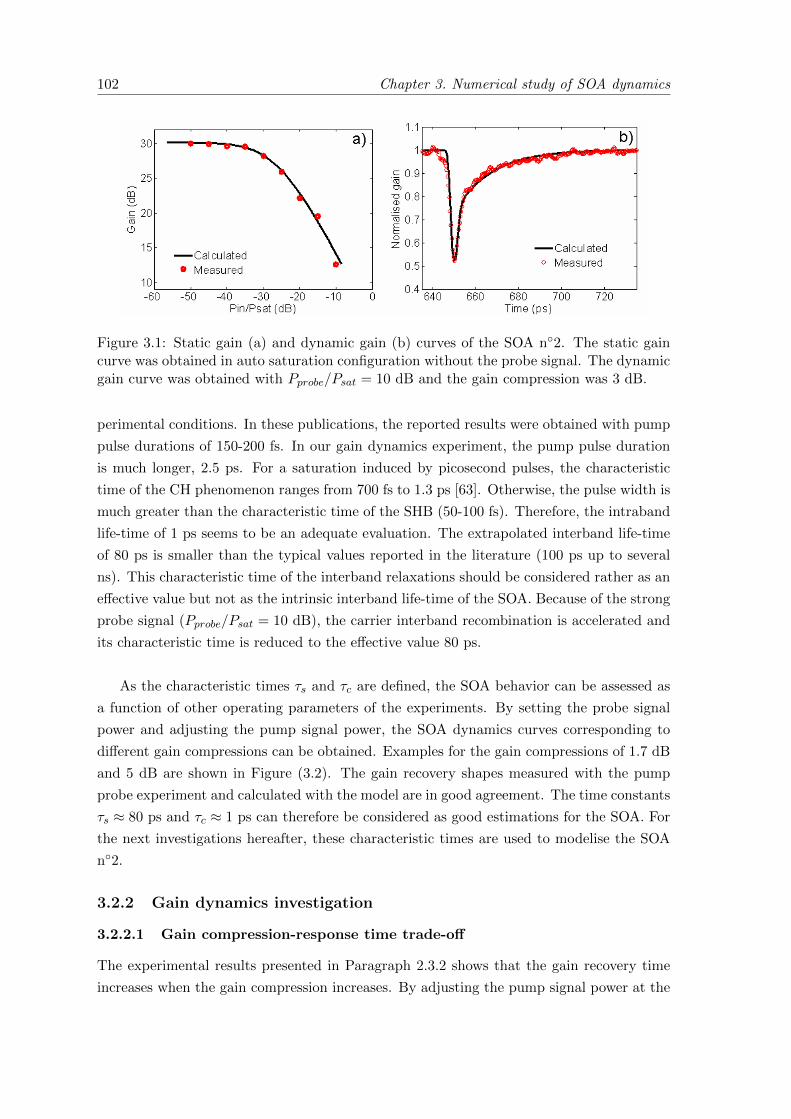
102 Chapter 3. Numerical study of SOA dynamics
Figure 3.1: Static gain (a) and dynamic gain (b) curves of the SOA n◦2. The static gaincurve was obtained in auto saturation configuration without the probe signal. The dynamicgain curve was obtained with Pprobe/Psat = 10 dB and the gain compression was 3 dB.
perimental conditions. In these publications, the reported results were obtained with pump
pulse durations of 150-200 fs. In our gain dynamics experiment, the pump pulse duration
is much longer, 2.5 ps. For a saturation induced by picosecond pulses, the characteristic
time of the CH phenomenon ranges from 700 fs to 1.3 ps [63]. Otherwise, the pulse width is
much greater than the characteristic time of the SHB (50-100 fs). Therefore, the intraband
life-time of 1 ps seems to be an adequate evaluation. The extrapolated interband life-time
of 80 ps is smaller than the typical values reported in the literature (100 ps up to several
ns). This characteristic time of the interband relaxations should be considered rather as an
effective value but not as the intrinsic interband life-time of the SOA. Because of the strong
probe signal (Pprobe/Psat = 10 dB), the carrier interband recombination is accelerated and
its characteristic time is reduced to the effective value 80 ps.
As the characteristic times τs and τc are defined, the SOA behavior can be assessed as
a function of other operating parameters of the experiments. By setting the probe signal
power and adjusting the pump signal power, the SOA dynamics curves corresponding to
different gain compressions can be obtained. Examples for the gain compressions of 1.7 dB
and 5 dB are shown in Figure (3.2). The gain recovery shapes measured with the pump
probe experiment and calculated with the model are in good agreement. The time constants
τs ≈ 80 ps and τc ≈ 1 ps can therefore be considered as good estimations for the SOA. For
the next investigations hereafter, these characteristic times are used to modelise the SOA
n◦2.
3.2.2 Gain dynamics investigation
3.2.2.1 Gain compression-response time trade-off
The experimental results presented in Paragraph 2.3.2 shows that the gain recovery time
increases when the gain compression increases. By adjusting the pump signal power at the
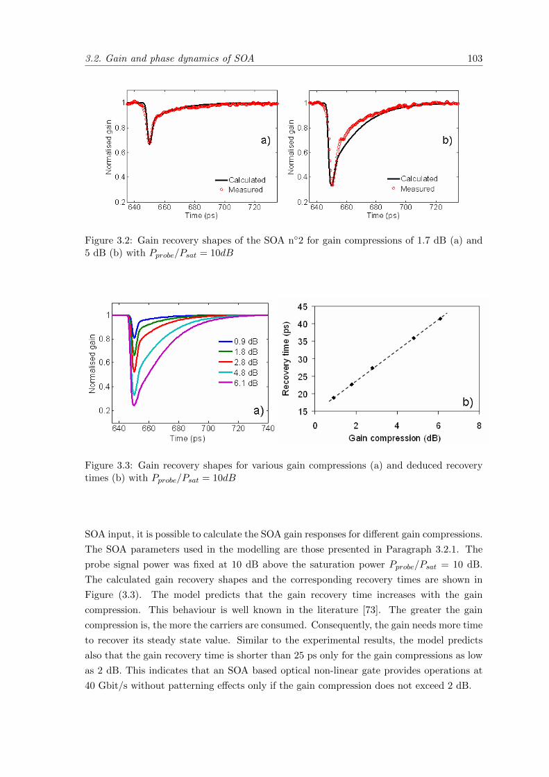
3.2. Gain and phase dynamics of SOA 103
Figure 3.2: Gain recovery shapes of the SOA n◦2 for gain compressions of 1.7 dB (a) and5 dB (b) with Pprobe/Psat = 10dB
Figure 3.3: Gain recovery shapes for various gain compressions (a) and deduced recoverytimes (b) with Pprobe/Psat = 10dB
SOA input, it is possible to calculate the SOA gain responses for different gain compressions.
The SOA parameters used in the modelling are those presented in Paragraph 3.2.1. The
probe signal power was fixed at 10 dB above the saturation power Pprobe/Psat = 10 dB.
The calculated gain recovery shapes and the corresponding recovery times are shown in
Figure (3.3). The model predicts that the gain recovery time increases with the gain
compression. This behaviour is well known in the literature [73]. The greater the gain
compression is, the more the carriers are consumed. Consequently, the gain needs more time
to recover its steady state value. Similar to the experimental results, the model predicts
also that the gain recovery time is shorter than 25 ps only for the gain compressions as low
as 2 dB. This indicates that an SOA based optical non-linear gate provides operations at
40 Gbit/s without patterning effects only if the gain compression does not exceed 2 dB.
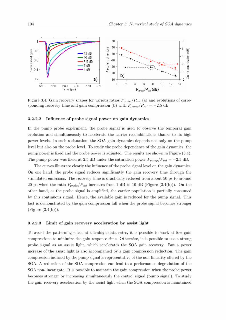
104 Chapter 3. Numerical study of SOA dynamics
Figure 3.4: Gain recovery shapes for various ratios Pprobe/Psat (a) and evolutions of corre-sponding recovery time and gain compression (b) with Ppump/Psat = −2.5 dB
3.2.2.2 Influence of probe signal power on gain dynamics
In the pump probe experiment, the probe signal is used to observe the temporal gain
evolution and simultaneously to accelerate the carrier recombinations thanks to its high
power levels. In such a situation, the SOA gain dynamics depends not only on the pump
level but also on the probe level. To study the probe dependence of the gain dynamics, the
pump power is fixed and the probe power is adjusted. The results are shown in Figure (3.4).
The pump power was fixed at 2.5 dB under the saturation power Ppump/Psat = −2.5 dB.
The curves illustrate clearly the influence of the probe signal level on the gain dynamics.
On one hand, the probe signal reduces significantly the gain recovery time through the
stimulated emissions. The recovery time is drastically reduced from about 50 ps to around
20 ps when the ratio Pprobe/Psat increases from 1 dB to 10 dB (Figure (3.4(b))). On the
other hand, as the probe signal is amplified, the carrier population is partially consumed
by this continuous signal. Hence, the available gain is reduced for the pump signal. This
fact is demonstrated by the gain compression fall when the probe signal becomes stronger
(Figure (3.4(b))).
3.2.2.3 Limit of gain recovery acceleration by assist light
To avoid the patterning effect at ultrahigh data rates, it is possible to work at low gain
compressions to minimize the gain response time. Otherwise, it is possible to use a strong
probe signal as an assist light, which accelerates the SOA gain recovery. But a power
increase of the assist light is also accompanied by a gain compression reduction. The gain
compression induced by the pump signal is representative of the non-linearity offered by the
SOA. A reduction of the SOA compression can lead to a performance degradation of the
SOA non-linear gate. It is possible to maintain the gain compression when the probe power
becomes stronger by increasing simultaneously the control signal (pump signal). To study
the gain recovery acceleration by the assist light when the SOA compression is maintained
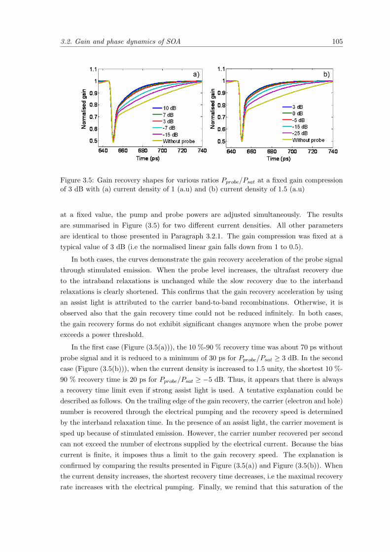
3.2. Gain and phase dynamics of SOA 105
Figure 3.5: Gain recovery shapes for various ratios Pprobe/Psat at a fixed gain compressionof 3 dB with (a) current density of 1 (a.u) and (b) current density of 1.5 (a.u)
at a fixed value, the pump and probe powers are adjusted simultaneously. The results
are summarised in Figure (3.5) for two different current densities. All other parameters
are identical to those presented in Paragraph 3.2.1. The gain compression was fixed at a
typical value of 3 dB (i.e the normalised linear gain falls down from 1 to 0.5).
In both cases, the curves demonstrate the gain recovery acceleration of the probe signal
through stimulated emission. When the probe level increases, the ultrafast recovery due
to the intraband relaxations is unchanged while the slow recovery due to the interband
relaxations is clearly shortened. This confirms that the gain recovery acceleration by using
an assist light is attributed to the carrier band-to-band recombinations. Otherwise, it is
observed also that the gain recovery time could not be reduced infinitely. In both cases,
the gain recovery forms do not exhibit significant changes anymore when the probe power
exceeds a power threshold.
In the first case (Figure (3.5(a))), the 10 %-90 % recovery time was about 70 ps without
probe signal and it is reduced to a minimum of 30 ps for Pprobe/Psat ≥ 3 dB. In the second
case (Figure (3.5(b))), when the current density is increased to 1.5 unity, the shortest 10 %-
90 % recovery time is 20 ps for Pprobe/Psat ≥ −5 dB. Thus, it appears that there is always
a recovery time limit even if strong assist light is used. A tentative explanation could be
described as follows. On the trailing edge of the gain recovery, the carrier (electron and hole)
number is recovered through the electrical pumping and the recovery speed is determined
by the interband relaxation time. In the presence of an assist light, the carrier movement is
sped up because of stimulated emission. However, the carrier number recovered per second
can not exceed the number of electrons supplied by the electrical current. Because the bias
current is finite, it imposes thus a limit to the gain recovery speed. The explanation is
confirmed by comparing the results presented in Figure (3.5(a)) and Figure (3.5(b)). When
the current density increases, the shortest recovery time decreases, i.e the maximal recovery
rate increases with the electrical pumping. Finally, we remind that this saturation of the
106 Chapter 3. Numerical study of SOA dynamics
gain recovery speed has been observed experimentally and presented in Paragraph 2.3.8.
3.2.3 Phase dynamics investigation
3.2.3.1 Rate equation of phase evolution
Following the developments in [15], the signal phase evolution is governed by Equation (3-
16):∂φ
∂z= −1
2αg (3-16)
Because of the time dependence of the differential gain g (z, τ), the phase is consequently
time dependent. In this case, the authors represent the coupling between the gain and the
induced phase depending only on one factor α. Otherwise, it was demonstrated previously
that the gain compression is attributed to both interband and intraband relaxations. The
refractive index change induced by the carrier changes results in a phase modulation of the
optical signal. In the literature, it is shown that the phase changes (via the index changes)
related to the intraband and interband gain suppression are represented by different coupling
factors [58], [62]. Therefore, it should be more accurate to consider two different coupling
factors: α related to the carrier change due to the interband transitions and αT related
to the carrier change due to the intraband transitions. Moreover, if the operation point is
close to the amplifier gain peak, the spectral hole burning induced by the carrier depletion
is symmetric and then the SHB does not contribute to the index change. Consequently,
the phase change induced by the intraband processes is dominated by the CH phenomenon.
The differential gain could be expressed by Equation (3-17).
g = glin + gnonlin =Γa
VN1 (3-17)
and using N1 = ∆N +NsU deduced from Equation (3-4), we obtain Equation (3-18):
glin =Γa
VUNs (3-18)
and
gnonlin =Γa
V∆N (3-19)
Similarly to the gain, the phase change induced by the refractive index change is then
expressed by Equation (3-20).
∂ϕ
∂z= −Γa
2V(αT∆N + αUNs) (3-20)
We remind that Ns is the total carrier population and ∆N is the deviation from thermal
equilibrium due to optical pulses. The first and the second terms on the right side of
Equation (3-20) correspond respectively to the contributions of intraband and interband
processes to the total phase changes. Time dependence of N1 is deduced from numerical
solution of Equation (3-15). The evolution of is the solution of Equation (3-21).
∂Ns
∂t=I
q− PN1
Es− Ns
τs(3-21)
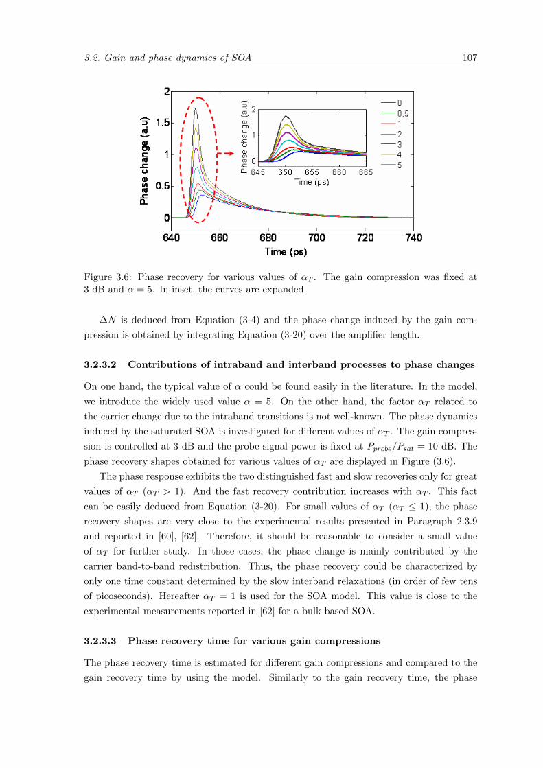
3.2. Gain and phase dynamics of SOA 107
Figure 3.6: Phase recovery for various values of αT . The gain compression was fixed at3 dB and α = 5. In inset, the curves are expanded.
∆N is deduced from Equation (3-4) and the phase change induced by the gain com-
pression is obtained by integrating Equation (3-20) over the amplifier length.
3.2.3.2 Contributions of intraband and interband processes to phase changes
On one hand, the typical value of α could be found easily in the literature. In the model,
we introduce the widely used value α = 5. On the other hand, the factor αT related to
the carrier change due to the intraband transitions is not well-known. The phase dynamics
induced by the saturated SOA is investigated for different values of αT . The gain compres-
sion is controlled at 3 dB and the probe signal power is fixed at Pprobe/Psat = 10 dB. The
phase recovery shapes obtained for various values of αT are displayed in Figure (3.6).
The phase response exhibits the two distinguished fast and slow recoveries only for great
values of αT (αT > 1). And the fast recovery contribution increases with αT . This fact
can be easily deduced from Equation (3-20). For small values of αT (αT ≤ 1), the phase
recovery shapes are very close to the experimental results presented in Paragraph 2.3.9
and reported in [60], [62]. Therefore, it should be reasonable to consider a small value
of αT for further study. In those cases, the phase change is mainly contributed by the
carrier band-to-band redistribution. Thus, the phase recovery could be characterized by
only one time constant determined by the slow interband relaxations (in order of few tens
of picoseconds). Hereafter αT = 1 is used for the SOA model. This value is close to the
experimental measurements reported in [62] for a bulk based SOA.
3.2.3.3 Phase recovery time for various gain compressions
The phase recovery time is estimated for different gain compressions and compared to the
gain recovery time by using the model. Similarly to the gain recovery time, the phase
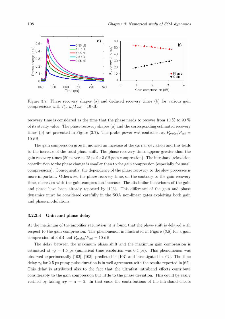
108 Chapter 3. Numerical study of SOA dynamics
Figure 3.7: Phase recovery shapes (a) and deduced recovery times (b) for various gaincompressions with Pprobe/Psat = 10 dB
recovery time is considered as the time that the phase needs to recover from 10 % to 90 %
of its steady value. The phase recovery shapes (a) and the corresponding estimated recovery
times (b) are presented in Figure (3.7). The probe power was controlled at Pprobe/Psat =
10 dB.
The gain compression growth induced an increase of the carrier deviation and this leads
to the increase of the total phase shift. The phase recovery times appear greater than the
gain recovery times (50 ps versus 25 ps for 3 dB gain compression). The intraband relaxation
contribution to the phase change is smaller than to the gain compression (especially for small
compressions). Consequently, the dependence of the phase recovery to the slow processes is
more important. Otherwise, the phase recovery time, on the contrary to the gain recovery
time, decreases with the gain compression increase. The dissimilar behaviours of the gain
and phase have been already reported by [106]. This difference of the gain and phase
dynamics must be considered carefully in the SOA non-linear gates exploiting both gain
and phase modulations.
3.2.3.4 Gain and phase delay
At the maximum of the amplifier saturation, it is found that the phase shift is delayed with
respect to the gain compression. The phenomenon is illustrated in Figure (3.8) for a gain
compression of 3 dB and Pprobe/Psat = 10 dB.
The delay between the maximum phase shift and the maximum gain compression is
estimated at τd = 1.5 ps (numerical time resolution was 0.4 ps). This phenomenon was
observed experimentally [102], [103], predicted in [107] and investigated in [62]. The time
delay τd for 2.5 ps pump pulse duration is in well agreement with the results reported in [62].
This delay is attributed also to the fact that the ultrafast intraband effects contribute
considerably to the gain compression but little to the phase deviation. This could be easily
verified by taking αT = α = 5. In that case, the contributions of the intraband effects
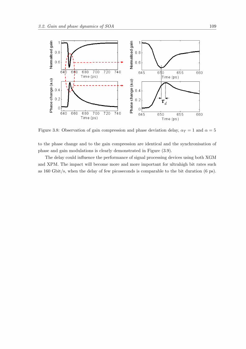
3.2. Gain and phase dynamics of SOA 109
Figure 3.8: Observation of gain compression and phase deviation delay, αT = 1 and α = 5
to the phase change and to the gain compression are identical and the synchronisation of
phase and gain modulations is clearly demonstrated in Figure (3.9).
The delay could influence the performance of signal processing devices using both XGM
and XPM. The impact will become more and more important for ultrahigh bit rates such
as 160 Gbit/s, when the delay of few picoseconds is comparable to the bit duration (6 ps).
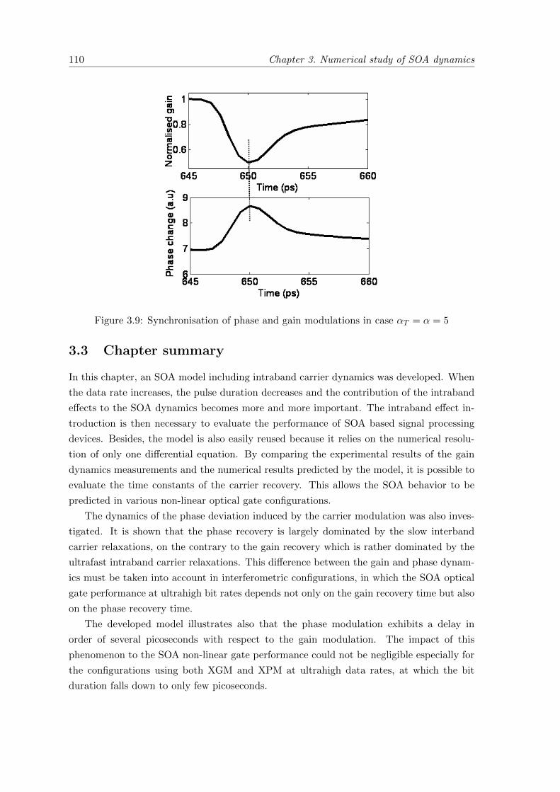
110 Chapter 3. Numerical study of SOA dynamics
Figure 3.9: Synchronisation of phase and gain modulations in case αT = α = 5
3.3 Chapter summary
In this chapter, an SOA model including intraband carrier dynamics was developed. When
the data rate increases, the pulse duration decreases and the contribution of the intraband
effects to the SOA dynamics becomes more and more important. The intraband effect in-
troduction is then necessary to evaluate the performance of SOA based signal processing
devices. Besides, the model is also easily reused because it relies on the numerical resolu-
tion of only one differential equation. By comparing the experimental results of the gain
dynamics measurements and the numerical results predicted by the model, it is possible to
evaluate the time constants of the carrier recovery. This allows the SOA behavior to be
predicted in various non-linear optical gate configurations.
The dynamics of the phase deviation induced by the carrier modulation was also inves-
tigated. It is shown that the phase recovery is largely dominated by the slow interband
carrier relaxations, on the contrary to the gain recovery which is rather dominated by the
ultrafast intraband carrier relaxations. This difference between the gain and phase dynam-
ics must be taken into account in interferometric configurations, in which the SOA optical
gate performance at ultrahigh bit rates depends not only on the gain recovery time but also
on the phase recovery time.
The developed model illustrates also that the phase modulation exhibits a delay in
order of several picoseconds with respect to the gain modulation. The impact of this
phenomenon to the SOA non-linear gate performance could not be negligible especially for
the configurations using both XGM and XPM at ultrahigh data rates, at which the bit
duration falls down to only few picoseconds.
Chapter 4
Investigation of SOA optical gates
for 2R regeneration at 40 Gbit/s
Gain non-linearity and fast response make SOA a good candidate as a non-linear optical
gate in signal processing functions. Experimental characterisations presented in Chapter 2
show clearly the high gain non-linearity characteristic of the studied SOAs. In particular,
short time responses of 20 ps for the bulk based SOA and of 3 ps for the long quantum-dot
SOA were demonstrated. These results indicate that SOA based non-linear optical gates
for bit by bit signal processing at ultrahigh bit rates beyond 40 Gbit/s could be possible.
Many devices have been reported in SOA interferometric gates [108], [109], [110] and have
demonstrated regeneration efficiency. However, the interferometric configurations require
in general several SOAs. A simpler solution for 2R regeneration could be achieved by cas-
cading an SOA and a Saturable Absorber (SA) [111], [112]. A 2R regenerator based on that
scheme demonstrated its regeneration efficiency in a transmission link at 10 Gbit/s [10]. In
this chapter, regeneration potential of non-linear optical gates at 40 Gbit/s based on SOA
in self-saturation is assessed experimentally and numerically. Noise compression effect of an
SOA gate is demonstrated first. Assessment of two non-linear optical gate configurations
for 2R regeneration is then presented. The regenerators are based on cascades of an SOA
and an SA.
According to the gain dynamics results presented in Chapter 2, the long quantum-dot
SOA (SOA n◦5) exhibits the shortest recovery time and hence appears as an appropriate
sample for ultrahigh speed operations. However, the available SOA exhibits an excessive
gain ripple of at least 6 dB at its typical bias currents. The strong gain ripple will add
large undesirable noise to the signal passing through the SOA. Therefore, the long QD SOA
sample could not be used in signal regeneration experiments. Among the other SOAs, the
highly confined bulk based SOA (SOA n◦2) appears as the best candidate for a regeneration
experiment at 40 Gbit/s. It exhibits lower ripple levels compared to the long QD SOA and
gain recovery times smaller than 25 ps at maximum bias current. Indeed, this SOA is the
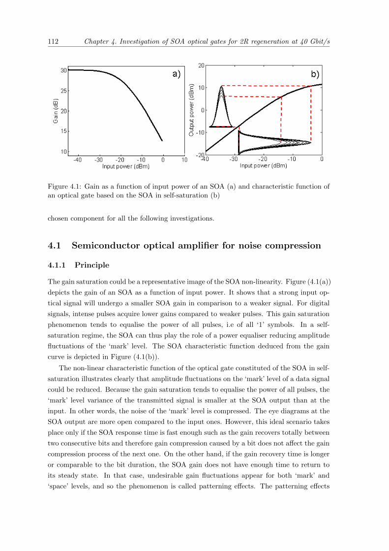
112 Chapter 4. Investigation of SOA optical gates for 2R regeneration at 40 Gbit/s
Figure 4.1: Gain as a function of input power of an SOA (a) and characteristic function ofan optical gate based on the SOA in self-saturation (b)
chosen component for all the following investigations.
4.1 Semiconductor optical amplifier for noise compression
4.1.1 Principle
The gain saturation could be a representative image of the SOA non-linearity. Figure (4.1(a))
depicts the gain of an SOA as a function of input power. It shows that a strong input op-
tical signal will undergo a smaller SOA gain in comparison to a weaker signal. For digital
signals, intense pulses acquire lower gains compared to weaker pulses. This gain saturation
phenomenon tends to equalise the power of all pulses, i.e of all ‘1’ symbols. In a self-
saturation regime, the SOA can thus play the role of a power equaliser reducing amplitude
fluctuations of the ‘mark’ level. The SOA characteristic function deduced from the gain
curve is depicted in Figure (4.1(b)).
The non-linear characteristic function of the optical gate constituted of the SOA in self-
saturation illustrates clearly that amplitude fluctuations on the ‘mark’ level of a data signal
could be reduced. Because the gain saturation tends to equalise the power of all pulses, the
‘mark’ level variance of the transmitted signal is smaller at the SOA output than at the
input. In other words, the noise of the ‘mark’ level is compressed. The eye diagrams at the
SOA output are more open compared to the input ones. However, this ideal scenario takes
place only if the SOA response time is fast enough such as the gain recovers totally between
two consecutive bits and therefore gain compression caused by a bit does not affect the gain
compression process of the next one. On the other hand, if the gain recovery time is longer
or comparable to the bit duration, the SOA gain does not have enough time to return to
its steady state. In that case, undesirable gain fluctuations appear for both ‘mark’ and
‘space’ levels, and so the phenomenon is called patterning effects. The patterning effects
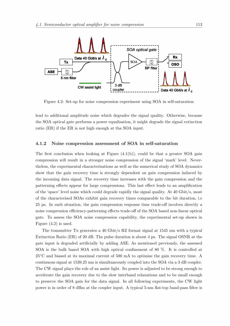
4.1. Semiconductor optical amplifier for noise compression 113
3 dB coupler
SOA
CW assist light
BP filter
Rx
OSO
Data 40 Gbit/s at 0λ
Data 40 Gbit/s at 0λ
SOA optical gate
Tx
ASE
5 nm filter
3 dB coupler
SOA
CW assist lightCW assist light
BP filterBP filter
RxRx
OSOOSO
Data 40 Gbit/s at 0λData 40 Gbit/s at 0λData 40 Gbit/s at 0λ
Data 40 Gbit/s at 0λData 40 Gbit/s at 0λ
SOA optical gate
Tx
ASE
5 nm filter
Tx
ASE
5 nm filter5 nm filter
Figure 4.2: Set-up for noise compression experiment using SOA in self-saturation
lead to additional amplitude noise which degrades the signal quality. Otherwise, because
the SOA optical gate performs a power equalisation, it might degrade the signal extinction
ratio (ER) if the ER is not high enough at tha SOA input.
4.1.2 Noise compression assessment of SOA in self-saturation
The first conclusion when looking at Figure (4.1(b)), could be that a greater SOA gain
compression will result in a stronger noise compression of the signal ‘mark’ level. Never-
theless, the experimental characterisations as well as the numerical study of SOA dynamics
show that the gain recovery time is strongly dependent on gain compression induced by
the incoming data signal. The recovery time increases with the gain compression and the
patterning effects appear for large compressions. This last effect leads to an amplification
of the ‘space’ level noise which could degrade rapidly the signal quality. At 40 Gbit/s, most
of the characterised SOAs exhibit gain recovery times comparable to the bit duration, i.e
25 ps. In such situation, the gain compression response time trade-off involves directly a
noise compression efficiency-patterning effects trade-off of the SOA based non-linear optical
gate. To assess the SOA noise compression capability, the experimental set-up shown in
Figure (4.2) is used.
The transmitter Tx generates a 40 Gbit/s RZ format signal at 1545 nm with a typical
Extinction Ratio (ER) of 20 dB. The pulse duration is about 4 ps. The signal OSNR at the
gate input is degraded artificially by adding ASE. As mentioned previously, the assessed
SOA is the bulk based SOA with high optical confinement of 80 %. It is controlled at
25◦C and biased at its maximal current of 500 mA to optimise the gain recovery time. A
continuous signal at 1539.25 nm is simultaneously coupled into the SOA via a 3 dB coupler.
The CW signal plays the role of an assist light. Its power is adjusted to be strong enough to
accelerate the gain recovery due to the slow interband relaxations and to be small enough
to preserve the SOA gain for the data signal. In all following experiments, the CW light
power is in order of 8 dBm at the coupler input. A typical 5-nm flat-top band-pass filter is
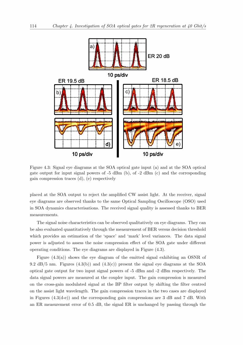
114 Chapter 4. Investigation of SOA optical gates for 2R regeneration at 40 Gbit/s
10 ps/div
a)
10 ps/div
b)
d)
10 ps/div
c)
e)
ER 20 dB
ER 19.5 dB ER 18.5 dB10 ps/div
a)
10 ps/div
b)
d)
10 ps/div
c)
e)
10 ps/div
a)
10 ps/div
a)
10 ps/div
b)
d)
10 ps/div
c)
e)
10 ps/div
b)
d)
10 ps/div
b)
d)
10 ps/div
c)
e)
10 ps/div
c)
e)
c)
e)
ER 20 dB
ER 19.5 dB ER 18.5 dB
Figure 4.3: Signal eye diagrams at the SOA optical gate input (a) and at the SOA opticalgate output for input signal powers of -5 dBm (b), of -2 dBm (c) and the correspondinggain compression traces (d), (e) respectively
placed at the SOA output to reject the amplified CW assist light. At the receiver, signal
eye diagrams are observed thanks to the same Optical Sampling Oscilloscope (OSO) used
in SOA dynamics characterisations. The received signal quality is assessed thanks to BER
measurements.
The signal noise characteristics can be observed qualitatively on eye diagrams. They can
be also evaluated quantitatively through the measurement of BER versus decision threshold
which provides an estimation of the ‘space’ and ‘mark’ level variances. The data signal
power is adjusted to assess the noise compression effect of the SOA gate under different
operating conditions. The eye diagrams are displayed in Figure (4.3).
Figure (4.3(a)) shows the eye diagram of the emitted signal exhibiting an OSNR of
9.2 dB/5 nm. Figures (4.3(b)) and (4.3(c)) present the signal eye diagrams at the SOA
optical gate output for two input signal powers of -5 dBm and -2 dBm respectively. The
data signal powers are measured at the coupler input. The gain compression is measured
on the cross-gain modulated signal at the BP filter output by shifting the filter centred
on the assist light wavelength. The gain compression traces in the two cases are displayed
in Figures (4.3(d-e)) and the corresponding gain compressions are 3 dB and 7 dB. With
an ER measurement error of 0.5 dB, the signal ER is unchanged by passing through the
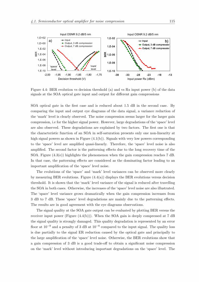
4.1. Semiconductor optical amplifier for noise compression 115
OSNR 9.2 dB/5 nm
1,E-10
1,E-08
1,E-06
1,E-04
1,E-02
1,E+00
1,E+02
-2,00 -1,95 -1,90 -1,85 -1,80 -1,75Decision threshold (V)
BER
InputOutput, 3 dB compressionOutput, 7 dB compression
‘space’level
‘mark’level
OSNR 9.2 dB/5 nm
1,E-10
1,E-08
1,E-06
1,E-04
1,E-02
-38 -33 -28 -23 -18 -13Input power Rx (dBm)
BE
R
InputOutput, 3 dB compressionOutput, 7 dB compression
Decision threshold (V) Input power Rx (dBm)
a) b)
Input OSNR 9.2 dB/5 nm Input OSNR 9.2 dB/5 nmOSNR 9.2 dB/5 nm
1,E-10
1,E-08
1,E-06
1,E-04
1,E-02
1,E+00
1,E+02
-2,00 -1,95 -1,90 -1,85 -1,80 -1,75Decision threshold (V)
BER
InputOutput, 3 dB compressionOutput, 7 dB compression
‘space’level
‘mark’level
OSNR 9.2 dB/5 nm
1,E-10
1,E-08
1,E-06
1,E-04
1,E-02
1,E+00
1,E+02
-2,00 -1,95 -1,90 -1,85 -1,80 -1,75Decision threshold (V)
BER
InputOutput, 3 dB compressionOutput, 7 dB compression
‘space’level
‘mark’level
OSNR 9.2 dB/5 nm
1,E-10
1,E-08
1,E-06
1,E-04
1,E-02
-38 -33 -28 -23 -18 -13Input power Rx (dBm)
BE
R
InputOutput, 3 dB compressionOutput, 7 dB compression
Decision threshold (V) Input power Rx (dBm)
a) b)
Input OSNR 9.2 dB/5 nm Input OSNR 9.2 dB/5 nm
Figure 4.4: BER evolution vs decision threshold (a) and vs Rx input power (b) of the datasignals at the SOA optical gate input and output for different gain compressions
SOA optical gate in the first case and is reduced about 1.5 dB in the second case. By
comparing the input and output eye diagrams of the data signal, a variance reduction of
the ‘mark’ level is clearly observed. The noise compression seems larger for the larger gain
compression, i.e for the higher signal power. However, large degradations of the ‘space’ level
are also observed. These degradations are explained by two factors. The first one is that
the characteristic function of an SOA in self-saturation presents only one non-linearity at
high signal powers as shown in Figure (4.1(b)). Signals with very low powers corresponding
to the ‘space’ level are amplified quasi-linearly. Therefore, the ‘space’ level noise is also
amplified. The second factor is the patterning effects due to the long recovery time of the
SOA. Figure (4.3(e)) highlights the phenomenon when the gain compression reaches 7 dB.
In that case, the patterning effects are considered as the dominating factor leading to an
important amplification of the ‘space’ level noise.
The evolutions of the ‘space’ and ‘mark’ level variances can be observed more clearly
by measuring BER evolutions. Figure (4.4(a)) displays the BER evolutions versus decision
threshold. It is shown that the ‘mark’ level variance of the signal is reduced after travelling
the SOA in both cases. Otherwise, the increases of the ‘space’ level noise are also illustrated.
The ‘space’ level variance grows dramatically when the gain compression increases from
3 dB to 7 dB. These ‘space’ level degradations are mainly due to the patterning effects.
The results are in good agreement with the eye diagrams observations.
The signal quality at the SOA gate output can be evaluated by plotting BER versus the
receiver input power (Figure (4.4(b))). When the SOA gain is deeply compressed at 7 dB
the signal quality is strongly damaged. This quality degradation is represented by an error
floor at 10−9 and a penalty of 3 dB at 10−8 compared to the input signal. The quality loss
is due partially to the signal ER reduction caused by the optical gate and principally to
the large amplification of the ‘space’ level noise. Otherwise, the BER evolutions show that
a gain compression of 3 dB is a good trade-off to obtain a significant noise compression
on the ‘mark’ level without introducing important degradations on the ‘space’ level. The
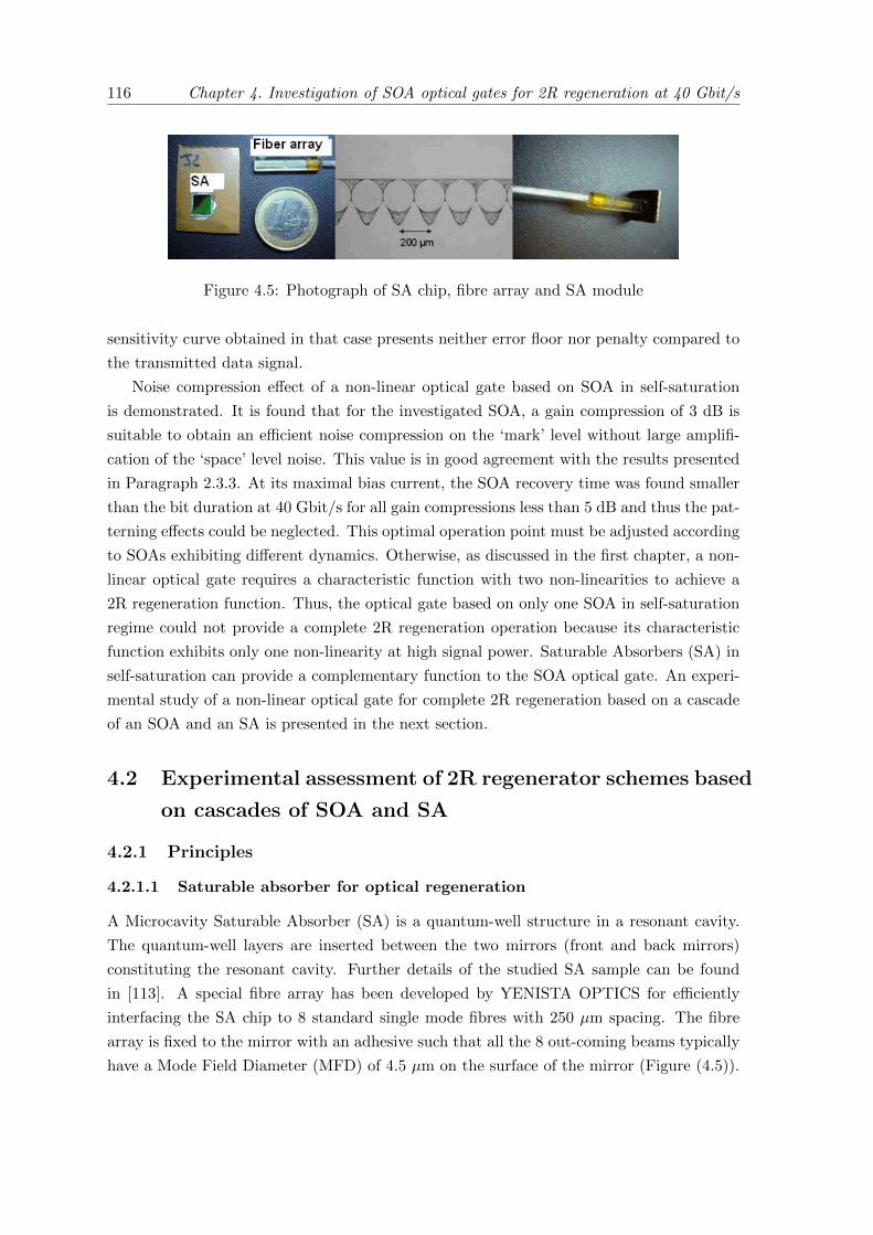
116 Chapter 4. Investigation of SOA optical gates for 2R regeneration at 40 Gbit/s
Figure 4.5: Photograph of SA chip, fibre array and SA module
sensitivity curve obtained in that case presents neither error floor nor penalty compared to
the transmitted data signal.
Noise compression effect of a non-linear optical gate based on SOA in self-saturation
is demonstrated. It is found that for the investigated SOA, a gain compression of 3 dB is
suitable to obtain an efficient noise compression on the ‘mark’ level without large amplifi-
cation of the ‘space’ level noise. This value is in good agreement with the results presented
in Paragraph 2.3.3. At its maximal bias current, the SOA recovery time was found smaller
than the bit duration at 40 Gbit/s for all gain compressions less than 5 dB and thus the pat-
terning effects could be neglected. This optimal operation point must be adjusted according
to SOAs exhibiting different dynamics. Otherwise, as discussed in the first chapter, a non-
linear optical gate requires a characteristic function with two non-linearities to achieve a
2R regeneration function. Thus, the optical gate based on only one SOA in self-saturation
regime could not provide a complete 2R regeneration operation because its characteristic
function exhibits only one non-linearity at high signal power. Saturable Absorbers (SA) in
self-saturation can provide a complementary function to the SOA optical gate. An experi-
mental study of a non-linear optical gate for complete 2R regeneration based on a cascade
of an SOA and an SA is presented in the next section.
4.2 Experimental assessment of 2R regenerator schemes based
on cascades of SOA and SA
4.2.1 Principles
4.2.1.1 Saturable absorber for optical regeneration
A Microcavity Saturable Absorber (SA) is a quantum-well structure in a resonant cavity.
The quantum-well layers are inserted between the two mirrors (front and back mirrors)
constituting the resonant cavity. Further details of the studied SA sample can be found
in [113]. A special fibre array has been developed by YENISTA OPTICS for efficiently
interfacing the SA chip to 8 standard single mode fibres with 250 µm spacing. The fibre
array is fixed to the mirror with an adhesive such that all the 8 out-coming beams typically
have a Mode Field Diameter (MFD) of 4.5 µm on the surface of the mirror (Figure (4.5)).
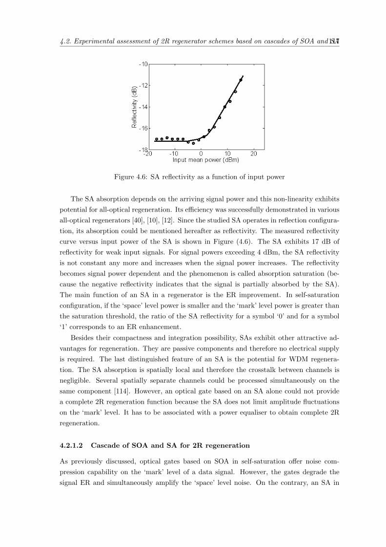
4.2. Experimental assessment of 2R regenerator schemes based on cascades of SOA and SA117
Figure 4.6: SA reflectivity as a function of input power
The SA absorption depends on the arriving signal power and this non-linearity exhibits
potential for all-optical regeneration. Its efficiency was successfully demonstrated in various
all-optical regenerators [40], [10], [12]. Since the studied SA operates in reflection configura-
tion, its absorption could be mentioned hereafter as reflectivity. The measured reflectivity
curve versus input power of the SA is shown in Figure (4.6). The SA exhibits 17 dB of
reflectivity for weak input signals. For signal powers exceeding 4 dBm, the SA reflectivity
is not constant any more and increases when the signal power increases. The reflectivity
becomes signal power dependent and the phenomenon is called absorption saturation (be-
cause the negative reflectivity indicates that the signal is partially absorbed by the SA).
The main function of an SA in a regenerator is the ER improvement. In self-saturation
configuration, if the ‘space’ level power is smaller and the ‘mark’ level power is greater than
the saturation threshold, the ratio of the SA reflectivity for a symbol ‘0’ and for a symbol
‘1’ corresponds to an ER enhancement.
Besides their compactness and integration possibility, SAs exhibit other attractive ad-
vantages for regeneration. They are passive components and therefore no electrical supply
is required. The last distinguished feature of an SA is the potential for WDM regenera-
tion. The SA absorption is spatially local and therefore the crosstalk between channels is
negligible. Several spatially separate channels could be processed simultaneously on the
same component [114]. However, an optical gate based on an SA alone could not provide
a complete 2R regeneration function because the SA does not limit amplitude fluctuations
on the ‘mark’ level. It has to be associated with a power equaliser to obtain complete 2R
regeneration.
4.2.1.2 Cascade of SOA and SA for 2R regeneration
As previously discussed, optical gates based on SOA in self-saturation offer noise com-
pression capability on the ‘mark’ level of a data signal. However, the gates degrade the
signal ER and simultaneously amplify the ‘space’ level noise. On the contrary, an SA in
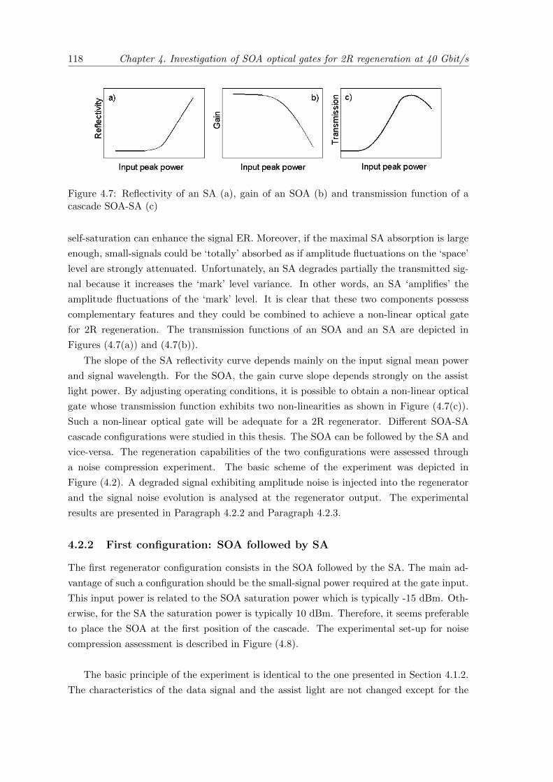
118 Chapter 4. Investigation of SOA optical gates for 2R regeneration at 40 Gbit/s
Figure 4.7: Reflectivity of an SA (a), gain of an SOA (b) and transmission function of acascade SOA-SA (c)
self-saturation can enhance the signal ER. Moreover, if the maximal SA absorption is large
enough, small-signals could be ‘totally’ absorbed as if amplitude fluctuations on the ‘space’
level are strongly attenuated. Unfortunately, an SA degrades partially the transmitted sig-
nal because it increases the ‘mark’ level variance. In other words, an SA ‘amplifies’ the
amplitude fluctuations of the ‘mark’ level. It is clear that these two components possess
complementary features and they could be combined to achieve a non-linear optical gate
for 2R regeneration. The transmission functions of an SOA and an SA are depicted in
Figures (4.7(a)) and (4.7(b)).
The slope of the SA reflectivity curve depends mainly on the input signal mean power
and signal wavelength. For the SOA, the gain curve slope depends strongly on the assist
light power. By adjusting operating conditions, it is possible to obtain a non-linear optical
gate whose transmission function exhibits two non-linearities as shown in Figure (4.7(c)).
Such a non-linear optical gate will be adequate for a 2R regenerator. Different SOA-SA
cascade configurations were studied in this thesis. The SOA can be followed by the SA and
vice-versa. The regeneration capabilities of the two configurations were assessed through
a noise compression experiment. The basic scheme of the experiment was depicted in
Figure (4.2). A degraded signal exhibiting amplitude noise is injected into the regenerator
and the signal noise evolution is analysed at the regenerator output. The experimental
results are presented in Paragraph 4.2.2 and Paragraph 4.2.3.
4.2.2 First configuration: SOA followed by SA
The first regenerator configuration consists in the SOA followed by the SA. The main ad-
vantage of such a configuration should be the small-signal power required at the gate input.
This input power is related to the SOA saturation power which is typically -15 dBm. Oth-
erwise, for the SA the saturation power is typically 10 dBm. Therefore, it seems preferable
to place the SOA at the first position of the cascade. The experimental set-up for noise
compression assessment is described in Figure (4.8).
The basic principle of the experiment is identical to the one presented in Section 4.1.2.
The characteristics of the data signal and the assist light are not changed except for the
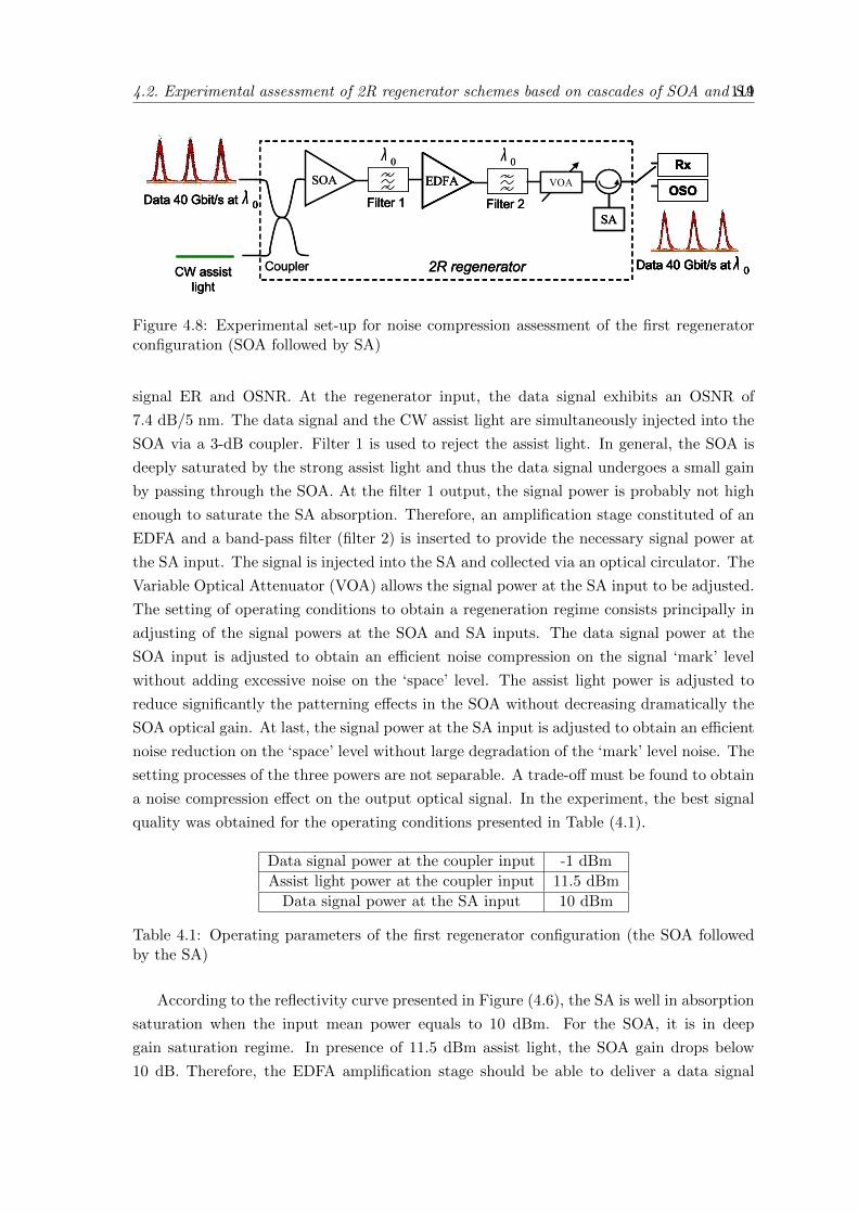
4.2. Experimental assessment of 2R regenerator schemes based on cascades of SOA and SA119
Coupler
SOA
CW assistlight
Filter 1Data 40 Gbit/s at 0λ
0λ
2R regenerator
SA
EDFA
Filter 2
0λ Rx
OSO
Data 40 Gbit/s at 0λ
VOA
Coupler
SOA
CW assistlight
CW assistlight
Filter 1Filter 1Data 40 Gbit/s at 0λData 40 Gbit/s at 0λData 40 Gbit/s at 0λ
0λ
2R regenerator2R regenerator
SASA
EDFAEDFA
Filter 2Filter 2
0λ Rx
OSO
Data 40 Gbit/s at 0λ
RxRx
OSOOSO
Data 40 Gbit/s at 0λData 40 Gbit/s at 0λData 40 Gbit/s at 0λ
VOAVOA
Figure 4.8: Experimental set-up for noise compression assessment of the first regeneratorconfiguration (SOA followed by SA)
signal ER and OSNR. At the regenerator input, the data signal exhibits an OSNR of
7.4 dB/5 nm. The data signal and the CW assist light are simultaneously injected into the
SOA via a 3-dB coupler. Filter 1 is used to reject the assist light. In general, the SOA is
deeply saturated by the strong assist light and thus the data signal undergoes a small gain
by passing through the SOA. At the filter 1 output, the signal power is probably not high
enough to saturate the SA absorption. Therefore, an amplification stage constituted of an
EDFA and a band-pass filter (filter 2) is inserted to provide the necessary signal power at
the SA input. The signal is injected into the SA and collected via an optical circulator. The
Variable Optical Attenuator (VOA) allows the signal power at the SA input to be adjusted.
The setting of operating conditions to obtain a regeneration regime consists principally in
adjusting of the signal powers at the SOA and SA inputs. The data signal power at the
SOA input is adjusted to obtain an efficient noise compression on the signal ‘mark’ level
without adding excessive noise on the ‘space’ level. The assist light power is adjusted to
reduce significantly the patterning effects in the SOA without decreasing dramatically the
SOA optical gain. At last, the signal power at the SA input is adjusted to obtain an efficient
noise reduction on the ‘space’ level without large degradation of the ‘mark’ level noise. The
setting processes of the three powers are not separable. A trade-off must be found to obtain
a noise compression effect on the output optical signal. In the experiment, the best signal
quality was obtained for the operating conditions presented in Table (4.1).
Data signal power at the coupler input -1 dBm
Assist light power at the coupler input 11.5 dBm
Data signal power at the SA input 10 dBm
Table 4.1: Operating parameters of the first regenerator configuration (the SOA followedby the SA)
According to the reflectivity curve presented in Figure (4.6), the SA is well in absorption
saturation when the input mean power equals to 10 dBm. For the SOA, it is in deep
gain saturation regime. In presence of 11.5 dBm assist light, the SOA gain drops below
10 dB. Therefore, the EDFA amplification stage should be able to deliver a data signal
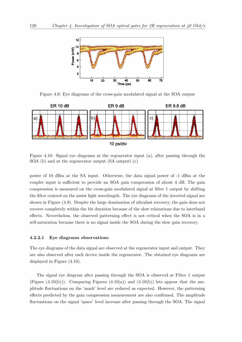
120 Chapter 4. Investigation of SOA optical gates for 2R regeneration at 40 Gbit/s
12
10
8
6
4
2
10 20 30 40 50 60 70
Pow
er (m
W)
Time (ps)
12
10
8
6
4
2
10 20 30 40 50 60 70
Pow
er (m
W)
Time (ps)
12
10
8
6
4
2
10 20 30 40 50 60 70
12
10
8
6
4
2
10 20 30 40 50 60 70
Pow
er (m
W)
Time (ps)
Figure 4.9: Eye diagrams of the cross-gain modulated signal at the SOA output
ER 10 dB ER 9 dB ER 9.8 dB
10 ps/div
a) b) c)
ER 10 dB ER 9 dB ER 9.8 dB
10 ps/div
a) b) c)
Figure 4.10: Signal eye diagrams at the regenerator input (a), after passing through theSOA (b) and at the regenerator output (SA output) (c)
power of 10 dBm at the SA input. Otherwise, the data signal power of -1 dBm at the
coupler input is sufficient to provide an SOA gain compression of about 4 dB. The gain
compression is measured on the cross-gain modulated signal at filter 1 output by shifting
the filter centred on the assist light wavelength. The eye diagrams of the inverted signal are
shown in Figure (4.9). Despite the large domination of ultrafast recovery, the gain does not
recover completely within the bit duration because of the slow relaxations due to interband
effects. Nevertheless, the observed patterning effect is not critical when the SOA is in a
self-saturation because there is no signal inside the SOA during the slow gain recovery.
4.2.2.1 Eye diagrams observations
The eye diagrams of the data signal are observed at the regenerator input and output. They
are also observed after each device inside the regenerator. The obtained eye diagrams are
displayed in Figure (4.10).
The signal eye diagram after passing through the SOA is observed at Filter 1 output
(Figure (4.10(b))). Comparing Figures (4.10(a)) and (4.10(b)) lets appear that the am-
plitude fluctuations on the ‘mark’ level are reduced as expected. However, the patterning
effects predicted by the gain compression measurement are also confirmed. The amplitude
fluctuations on the signal ‘space’ level increase after passing through the SOA. The signal
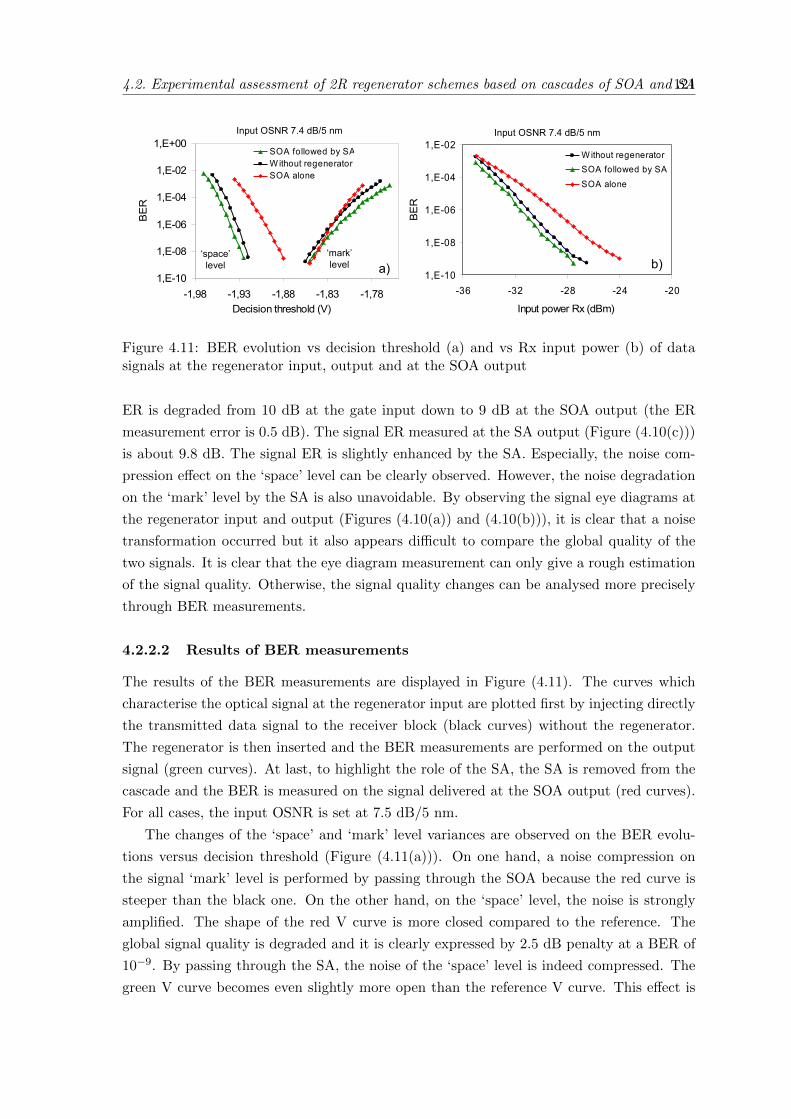
4.2. Experimental assessment of 2R regenerator schemes based on cascades of SOA and SA121
OSNR 7.4 dB/5 nm
1,E-10
1,E-08
1,E-06
1,E-04
1,E-02
1,E+00
-1,98 -1,93 -1,88 -1,83 -1,78Decision threshold (V)
BE
RSOA followed by SAW ithout regeneratorSOA alone
OSNR 7.4 dB/5 nm
1,E-10
1,E-08
1,E-06
1,E-04
1,E-02
-36 -32 -28 -24 -20
Input power Rx (dBm)
BE
R
W ithout regeneratorSOA followed by SA SOA alone
‘space’level
‘mark’level a) b)
Input OSNR 7.4 dB/5 nm Input OSNR 7.4 dB/5 nmOSNR 7.4 dB/5 nm
1,E-10
1,E-08
1,E-06
1,E-04
1,E-02
1,E+00
-1,98 -1,93 -1,88 -1,83 -1,78Decision threshold (V)
BE
RSOA followed by SAW ithout regeneratorSOA alone
OSNR 7.4 dB/5 nm
1,E-10
1,E-08
1,E-06
1,E-04
1,E-02
-36 -32 -28 -24 -20
Input power Rx (dBm)
BE
R
W ithout regeneratorSOA followed by SA SOA alone
‘space’level
‘mark’level a) b)
Input OSNR 7.4 dB/5 nm Input OSNR 7.4 dB/5 nm
Figure 4.11: BER evolution vs decision threshold (a) and vs Rx input power (b) of datasignals at the regenerator input, output and at the SOA output
ER is degraded from 10 dB at the gate input down to 9 dB at the SOA output (the ER
measurement error is 0.5 dB). The signal ER measured at the SA output (Figure (4.10(c)))
is about 9.8 dB. The signal ER is slightly enhanced by the SA. Especially, the noise com-
pression effect on the ‘space’ level can be clearly observed. However, the noise degradation
on the ‘mark’ level by the SA is also unavoidable. By observing the signal eye diagrams at
the regenerator input and output (Figures (4.10(a)) and (4.10(b))), it is clear that a noise
transformation occurred but it also appears difficult to compare the global quality of the
two signals. It is clear that the eye diagram measurement can only give a rough estimation
of the signal quality. Otherwise, the signal quality changes can be analysed more precisely
through BER measurements.
4.2.2.2 Results of BER measurements
The results of the BER measurements are displayed in Figure (4.11). The curves which
characterise the optical signal at the regenerator input are plotted first by injecting directly
the transmitted data signal to the receiver block (black curves) without the regenerator.
The regenerator is then inserted and the BER measurements are performed on the output
signal (green curves). At last, to highlight the role of the SA, the SA is removed from the
cascade and the BER is measured on the signal delivered at the SOA output (red curves).
For all cases, the input OSNR is set at 7.5 dB/5 nm.
The changes of the ‘space’ and ‘mark’ level variances are observed on the BER evolu-
tions versus decision threshold (Figure (4.11(a))). On one hand, a noise compression on
the signal ‘mark’ level is performed by passing through the SOA because the red curve is
steeper than the black one. On the other hand, on the ‘space’ level, the noise is strongly
amplified. The shape of the red V curve is more closed compared to the reference. The
global signal quality is degraded and it is clearly expressed by 2.5 dB penalty at a BER of
10−9. By passing through the SA, the noise of the ‘space’ level is indeed compressed. The
green V curve becomes even slightly more open than the reference V curve. This effect is
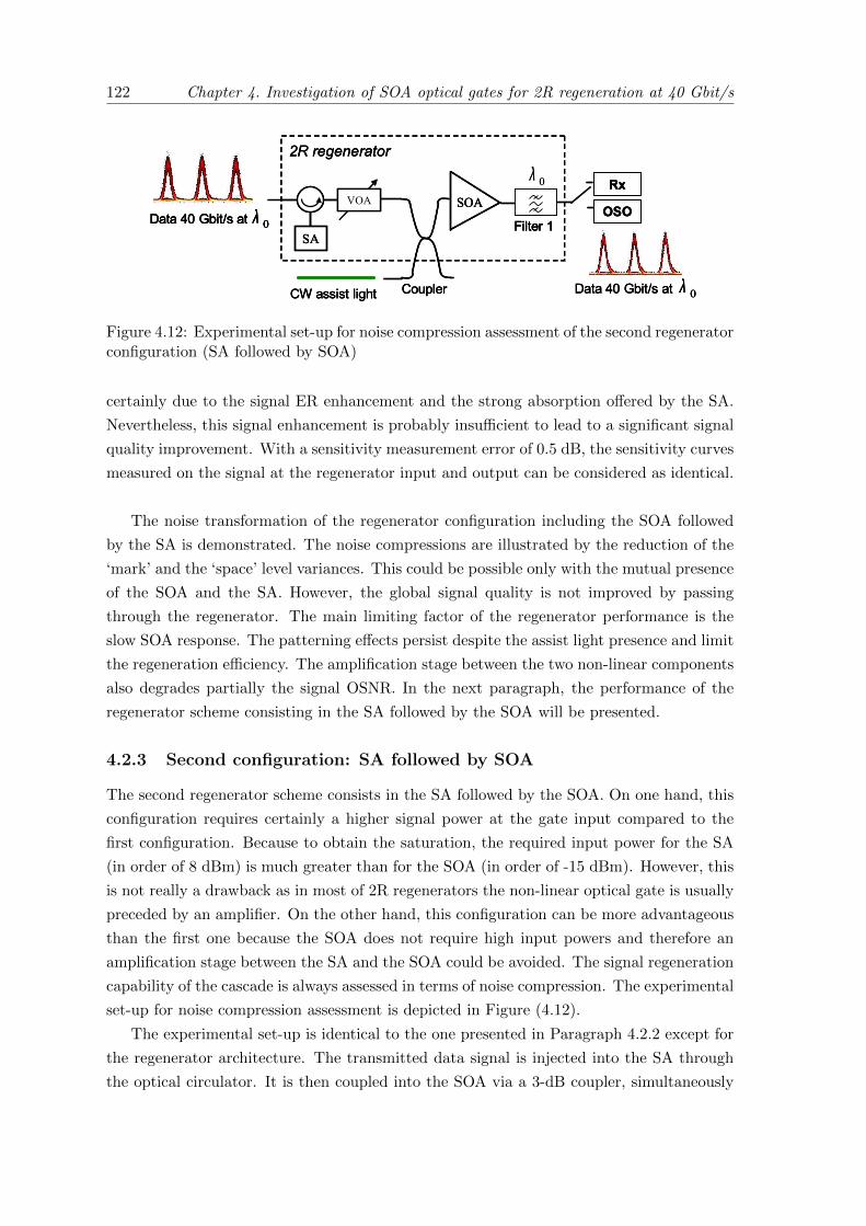
122 Chapter 4. Investigation of SOA optical gates for 2R regeneration at 40 Gbit/s
CouplerCW assist light
SOA
Filter 1
Rx
OSOData 40 Gbit/s at 0λ
Data 40 Gbit/s at 0λ
2R regenerator
SA
0λVOA
CouplerCouplerCW assist lightCW assist light
SOA
Filter 1
SOA
Filter 1Filter 1
RxRx
OSOOSOData 40 Gbit/s at 0λData 40 Gbit/s at 0λData 40 Gbit/s at 0λ
Data 40 Gbit/s at 0λData 40 Gbit/s at 0λ
2R regenerator2R regenerator
SASA
0λVOAVOA
Figure 4.12: Experimental set-up for noise compression assessment of the second regeneratorconfiguration (SA followed by SOA)
certainly due to the signal ER enhancement and the strong absorption offered by the SA.
Nevertheless, this signal enhancement is probably insufficient to lead to a significant signal
quality improvement. With a sensitivity measurement error of 0.5 dB, the sensitivity curves
measured on the signal at the regenerator input and output can be considered as identical.
The noise transformation of the regenerator configuration including the SOA followed
by the SA is demonstrated. The noise compressions are illustrated by the reduction of the
‘mark’ and the ‘space’ level variances. This could be possible only with the mutual presence
of the SOA and the SA. However, the global signal quality is not improved by passing
through the regenerator. The main limiting factor of the regenerator performance is the
slow SOA response. The patterning effects persist despite the assist light presence and limit
the regeneration efficiency. The amplification stage between the two non-linear components
also degrades partially the signal OSNR. In the next paragraph, the performance of the
regenerator scheme consisting in the SA followed by the SOA will be presented.
4.2.3 Second configuration: SA followed by SOA
The second regenerator scheme consists in the SA followed by the SOA. On one hand, this
configuration requires certainly a higher signal power at the gate input compared to the
first configuration. Because to obtain the saturation, the required input power for the SA
(in order of 8 dBm) is much greater than for the SOA (in order of -15 dBm). However, this
is not really a drawback as in most of 2R regenerators the non-linear optical gate is usually
preceded by an amplifier. On the other hand, this configuration can be more advantageous
than the first one because the SOA does not require high input powers and therefore an
amplification stage between the SA and the SOA could be avoided. The signal regeneration
capability of the cascade is always assessed in terms of noise compression. The experimental
set-up for noise compression assessment is depicted in Figure (4.12).
The experimental set-up is identical to the one presented in Paragraph 4.2.2 except for
the regenerator architecture. The transmitted data signal is injected into the SA through
the optical circulator. It is then coupled into the SOA via a 3-dB coupler, simultaneously
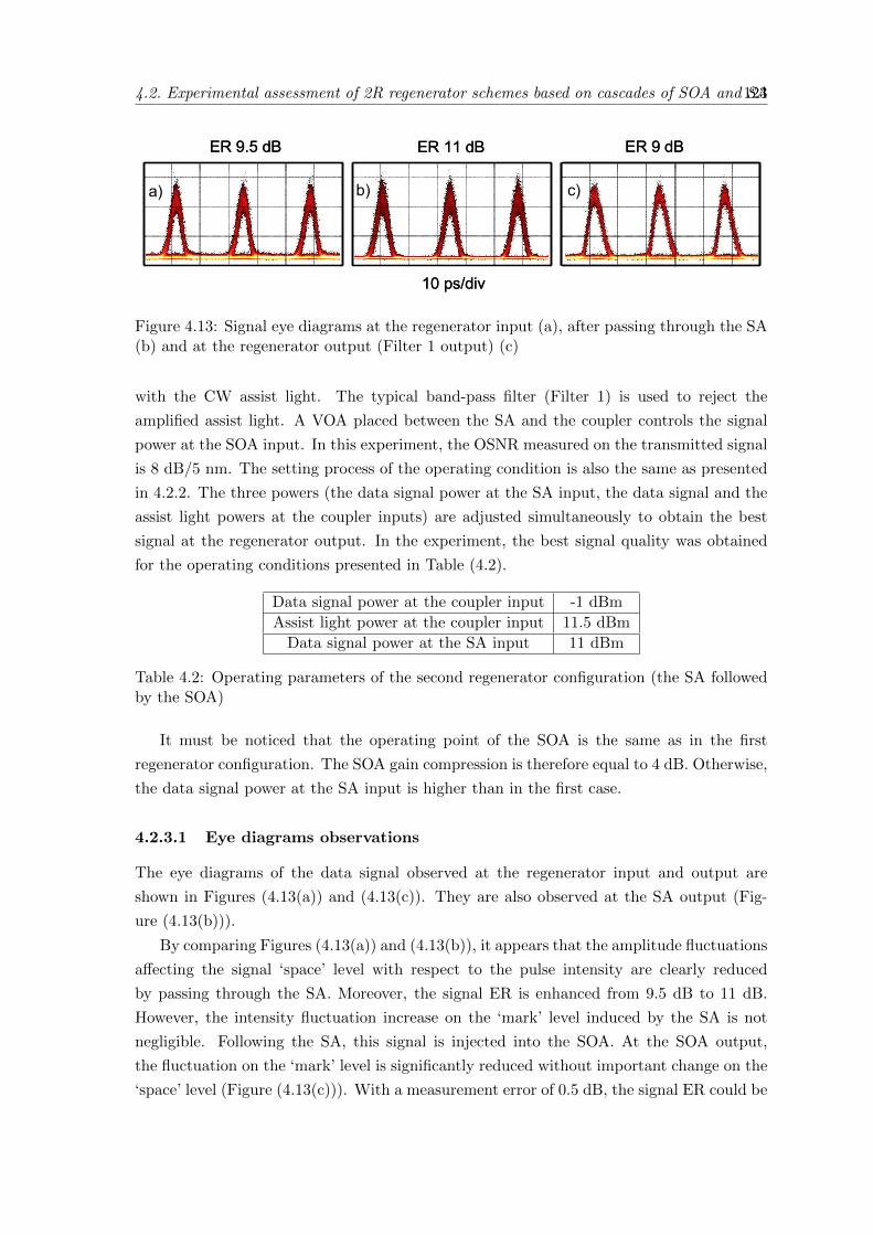
4.2. Experimental assessment of 2R regenerator schemes based on cascades of SOA and SA123
ER 9.5 dB ER 11 dB ER 9 dB
10 ps/div
a) b) c)
ER 9.5 dB ER 11 dB ER 9 dB
10 ps/div
a) b) c)
Figure 4.13: Signal eye diagrams at the regenerator input (a), after passing through the SA(b) and at the regenerator output (Filter 1 output) (c)
with the CW assist light. The typical band-pass filter (Filter 1) is used to reject the
amplified assist light. A VOA placed between the SA and the coupler controls the signal
power at the SOA input. In this experiment, the OSNR measured on the transmitted signal
is 8 dB/5 nm. The setting process of the operating condition is also the same as presented
in 4.2.2. The three powers (the data signal power at the SA input, the data signal and the
assist light powers at the coupler inputs) are adjusted simultaneously to obtain the best
signal at the regenerator output. In the experiment, the best signal quality was obtained
for the operating conditions presented in Table (4.2).
Data signal power at the coupler input -1 dBm
Assist light power at the coupler input 11.5 dBm
Data signal power at the SA input 11 dBm
Table 4.2: Operating parameters of the second regenerator configuration (the SA followedby the SOA)
It must be noticed that the operating point of the SOA is the same as in the first
regenerator configuration. The SOA gain compression is therefore equal to 4 dB. Otherwise,
the data signal power at the SA input is higher than in the first case.
4.2.3.1 Eye diagrams observations
The eye diagrams of the data signal observed at the regenerator input and output are
shown in Figures (4.13(a)) and (4.13(c)). They are also observed at the SA output (Fig-
ure (4.13(b))).
By comparing Figures (4.13(a)) and (4.13(b)), it appears that the amplitude fluctuations
affecting the signal ‘space’ level with respect to the pulse intensity are clearly reduced
by passing through the SA. Moreover, the signal ER is enhanced from 9.5 dB to 11 dB.
However, the intensity fluctuation increase on the ‘mark’ level induced by the SA is not
negligible. Following the SA, this signal is injected into the SOA. At the SOA output,
the fluctuation on the ‘mark’ level is significantly reduced without important change on the
‘space’ level (Figure (4.13(c))). With a measurement error of 0.5 dB, the signal ER could be
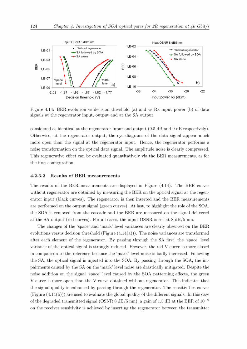
124 Chapter 4. Investigation of SOA optical gates for 2R regeneration at 40 Gbit/s
OSNR 8 dB/5 nm
1,E-10
1,E-08
1,E-06
1,E-04
1,E-02
-38 -34 -30 -26 -22Input power Rx (dBm)
BER
Reference
SA followed by SOASA alone
OSNR 8 dB/5 nm
1,E-09
1,E-07
1,E-05
1,E-03
1,E-01
-2,02 -1,97 -1,92 -1,87 -1,82 -1,77
Decision threshold (V)
BER
ReferenceSA followed by SOASA alone
‘space’level
‘mark’level a) b)
Input OSNR 8 dB/5 nmInput OSNR 8 dB/5 nm
Decision threshold (V) Input power Rx (dBm)
Without regenerator Without regenerator
OSNR 8 dB/5 nm
1,E-10
1,E-08
1,E-06
1,E-04
1,E-02
-38 -34 -30 -26 -22Input power Rx (dBm)
BER
Reference
SA followed by SOASA alone
OSNR 8 dB/5 nm
1,E-09
1,E-07
1,E-05
1,E-03
1,E-01
-2,02 -1,97 -1,92 -1,87 -1,82 -1,77
Decision threshold (V)
BER
ReferenceSA followed by SOASA alone
‘space’level
‘mark’level a) b)
Input OSNR 8 dB/5 nmInput OSNR 8 dB/5 nm
Decision threshold (V) Input power Rx (dBm)
OSNR 8 dB/5 nm
1,E-10
1,E-08
1,E-06
1,E-04
1,E-02
-38 -34 -30 -26 -22Input power Rx (dBm)
BER
Reference
SA followed by SOASA alone
OSNR 8 dB/5 nm
1,E-09
1,E-07
1,E-05
1,E-03
1,E-01
-2,02 -1,97 -1,92 -1,87 -1,82 -1,77
Decision threshold (V)
BER
ReferenceSA followed by SOASA alone
‘space’level
‘mark’level a) b)
OSNR 8 dB/5 nm
1,E-10
1,E-08
1,E-06
1,E-04
1,E-02
-38 -34 -30 -26 -22Input power Rx (dBm)
BER
Reference
SA followed by SOASA alone
OSNR 8 dB/5 nm
1,E-09
1,E-07
1,E-05
1,E-03
1,E-01
-2,02 -1,97 -1,92 -1,87 -1,82 -1,77
Decision threshold (V)
BER
ReferenceSA followed by SOASA alone
‘space’level
‘mark’level a) b)
Input OSNR 8 dB/5 nmInput OSNR 8 dB/5 nm
Decision threshold (V) Input power Rx (dBm)
Without regeneratorWithout regenerator Without regenerator
Figure 4.14: BER evolution vs decision threshold (a) and vs Rx input power (b) of datasignals at the regenerator input, output and at the SA output
considered as identical at the regenerator input and output (9.5 dB and 9 dB respectively).
Otherwise, at the regenerator output, the eye diagrams of the data signal appear much
more open than the signal at the regenerator input. Hence, the regenerator performs a
noise transformation on the optical data signal. The amplitude noise is clearly compressed.
This regenerative effect can be evaluated quantitatively via the BER measurements, as for
the first configuration.
4.2.3.2 Results of BER measurements
The results of the BER measurements are displayed in Figure (4.14). The BER curves
without regenerator are obtained by measuring the BER on the optical signal at the regen-
erator input (black curves). The regenerator is then inserted and the BER measurements
are performed on the output signal (green curves). At last, to highlight the role of the SOA,
the SOA is removed from the cascade and the BER are measured on the signal delivered
at the SA output (red curves). For all cases, the input OSNR is set at 8 dB/5 nm.
The changes of the ‘space’ and ‘mark’ level variances are clearly observed on the BER
evolutions versus decision threshold (Figure (4.14(a))). The noise variances are transformed
after each element of the regenerator. By passing through the SA first, the ‘space’ level
variance of the optical signal is strongly reduced. However, the red V curve is more closed
in comparison to the reference because the ‘mark’ level noise is badly increased. Following
the SA, the optical signal is injected into the SOA. By passing through the SOA, the im-
pairments caused by the SA on the ‘mark’ level noise are drastically mitigated. Despite the
noise addition on the signal ‘space’ level caused by the SOA patterning effects, the green
V curve is more open than the V curve obtained without regenerator. This indicates that
the signal quality is enhanced by passing through the regenerator. The sensitivities curves
(Figure (4.14(b))) are used to evaluate the global quality of the different signals. In this case
of the degraded transmitted signal (OSNR 8 dB/5 nm), a gain of 1.5 dB at the BER of 10−9
on the receiver sensitivity is achieved by inserting the regenerator between the transmitter
4.2. Experimental assessment of 2R regenerator schemes based on cascades of SOA and SA125
and receiver. This last result confirms that the signal quality is indeed enhanced thanks to
the SA-SOA cascade. The regenerative capability of the regenerator is thus demonstrated.
The noise transformation of the regenerator scheme consisting in the SA followed by the
SOA is illustrated at the bit rate of 40 Gbit/s. The noise compression effect, provided by the
regenerator, leads to a signal quality improvement. This quality enhancement is expressed
by a gain of 1.5 dB on the receiver sensitivity. It is found that the regenerator constituted
of the SOA and the SA exhibits regenerative properties thanks to the complementary non-
linearities of the two components. The regenerative effect in the second configuration (the
SA followed by the SOA) is better than in the first configuration (the SOA followed by the
SA). The ASE power added by the amplification stage, required in the first configuration,
was about 10 dBm and could not be neglected. This ASE noise addition degrades the
signal OSNR could be a tentative explanation for the performance difference between the
two regenerator schemes. At last, the limiting factor of the regenerator for operations at
higher bit rates (> 40 Gbit/s) is the SOA response time. It should be noticed also that the
SA response time is short enough for a 160 Gbit/s operation. By using an SOA exhibiting
shorter gain recovery times such as the long QD SOA (SOA n◦5), an operation at 160 Gbit/s
of the regenerator based on an SOA-SA cascade can be expected.
4.2.4 Spectrum deformation
The regenerators transform not only the temporal characteristics but also the spectral
characteristics of the optical signal. Figure (4.15) depicts the signal spectrum evolutions
by passing through the two previously studied regenerator configurations.
It appears that the optical spectrum at the regenerator output exhibits a asymmetry
while the signal spectrum at the regenerator input is symmetric. This spectral deforma-
tion is due to both non-linear components of the gates. As shown in the numerical study
(Chapter 3), the SOAs present a strong gain phase coupling. A gain modulation is always
accompanied by a phase modulation which induces chirp on the transmitted optical sig-
nal. The phenomenon is observed on the output signal spectrum by a dissymmetry and
a shift towards the longer wavelengths. On the other hand, the SA reflectivity spectrum
exhibits some selectivity as shown in Figure (4.16). Its bandwidth at half minimum is small
(about 5 nm) compared to the SOA bandwidth (about 30 nm). The spectral selectivity of
the SA reflectivity spectrum could lead to some signal spectrum deformations. However,
Figure (4.15) indicates that the SOA contribution to spectral deformations is dominant.
The spectral deformation effects can not be negligible especially when the regenerators are
cascaded. After each regenerator, the data signal spectrum is shifted further and further
towards the longer wavelengths and slips step by step out of the filters following the SOAs.
This last could lead to important signal attenuations and therefore limit the transmission
distance.
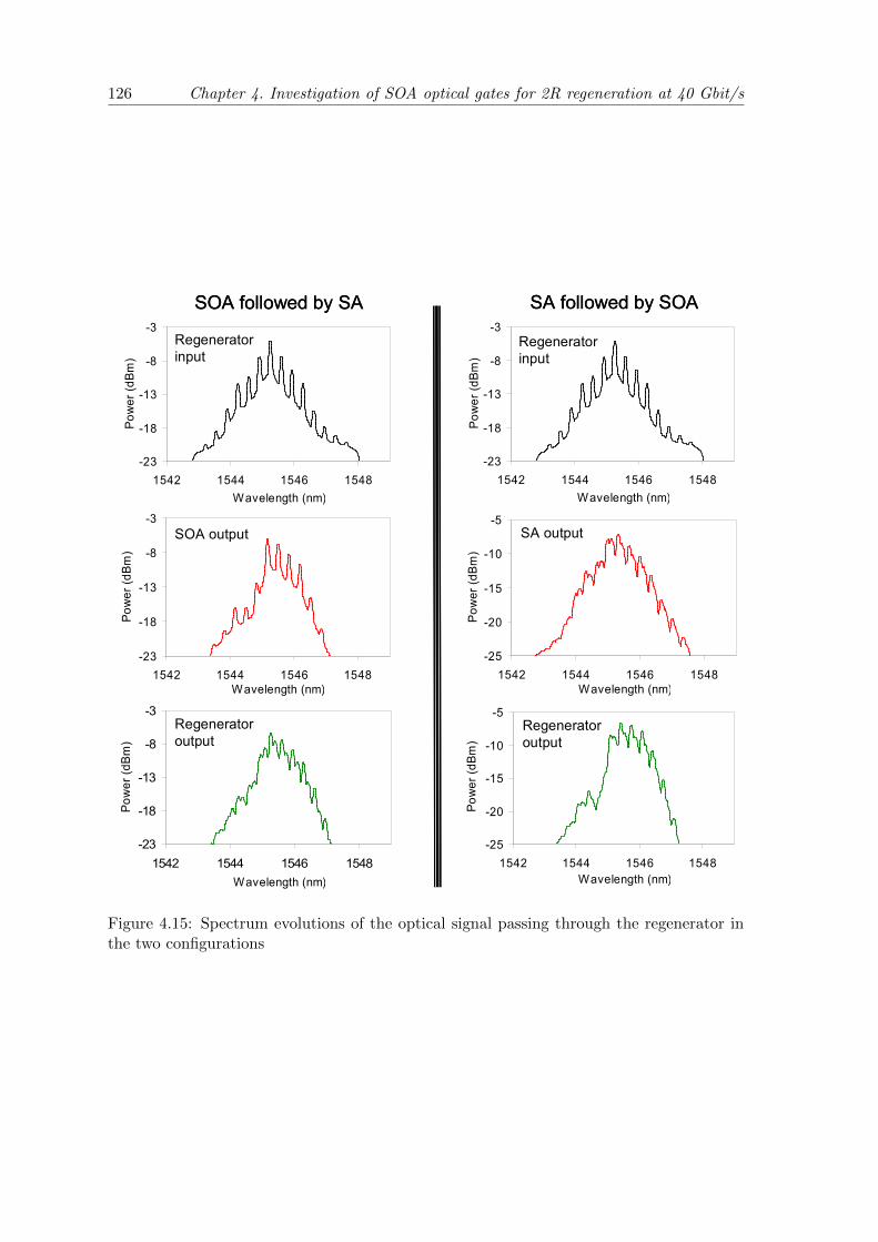
126 Chapter 4. Investigation of SOA optical gates for 2R regeneration at 40 Gbit/s
-23
-18
-13
-8
-3
1542 1544 1546 1548Wavelength (nm)
Pow
er (d
Bm)
-23
-18
-13
-8
-3
1542 1544 1546 1548Wavelength (nm)
Pow
er (d
Bm)
-23
-18
-13
-8
-3
1542 1544 1546 1548Wavelength (nm)
Pow
er (d
Bm
)
SOA followed by SA
Regeneratorinput
SOA output
Regeneratoroutput
-25
-20
-15
-10
-5
1542 1544 1546 1548Wavelength (nm)
Pow
er (d
Bm)
-25
-20
-15
-10
-5
1542 1544 1546 1548Wavelength (nm)
Pow
er (d
Bm
)-23
-18
-13
-8
-3
1542 1544 1546 1548Wavelength (nm)
Pow
er (d
Bm)
SA followed by SOA
SA output
Regeneratoroutput
Regeneratorinput
-23
-18
-13
-8
-3
1542 1544 1546 1548Wavelength (nm)
Pow
er (d
Bm)
-23
-18
-13
-8
-3
1542 1544 1546 1548Wavelength (nm)
Pow
er (d
Bm)
-23
-18
-13
-8
-3
1542 1544 1546 1548Wavelength (nm)
Pow
er (d
Bm
)
-23
-18
-13
-8
-3
1542 1544 1546 1548Wavelength (nm)
Pow
er (d
Bm)
-23
-18
-13
-8
-3
1542 1544 1546 1548Wavelength (nm)
Pow
er (d
Bm)
-23
-18
-13
-8
-3
1542 1544 1546 1548Wavelength (nm)
Pow
er (d
Bm
)
SOA followed by SA
Regeneratorinput
SOA output
Regeneratoroutput
-25
-20
-15
-10
-5
1542 1544 1546 1548Wavelength (nm)
Pow
er (d
Bm)
-25
-20
-15
-10
-5
1542 1544 1546 1548Wavelength (nm)
Pow
er (d
Bm
)-23
-18
-13
-8
-3
1542 1544 1546 1548Wavelength (nm)
Pow
er (d
Bm)
-25
-20
-15
-10
-5
1542 1544 1546 1548Wavelength (nm)
Pow
er (d
Bm)
-25
-20
-15
-10
-5
1542 1544 1546 1548Wavelength (nm)
Pow
er (d
Bm
)-23
-18
-13
-8
-3
1542 1544 1546 1548Wavelength (nm)
Pow
er (d
Bm)
SA followed by SOA
SA output
Regeneratoroutput
Regeneratorinput
Figure 4.15: Spectrum evolutions of the optical signal passing through the regenerator inthe two configurations
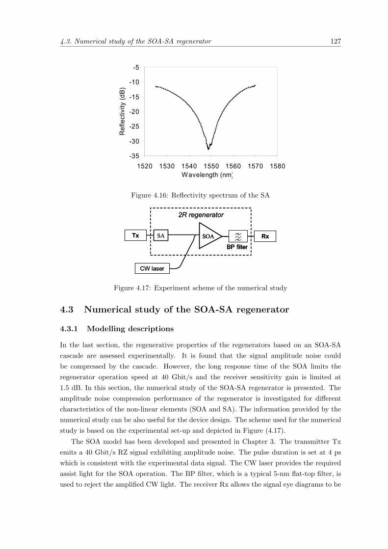
4.3. Numerical study of the SOA-SA regenerator 127
-35
-30
-25
-20
-15
-10
-5
1520 1530 1540 1550 1560 1570 1580Wavelength (nm)
Ref
lect
ivity
(dB)
Figure 4.16: Reflectivity spectrum of the SA
SOA
BP filter
Rx
2R regenerator
SATx
CW laser
SOA
BP filter
SOA
BP filterBP filter
Rx
2R regenerator
SATx
CW laser
Figure 4.17: Experiment scheme of the numerical study
4.3 Numerical study of the SOA-SA regenerator
4.3.1 Modelling descriptions
In the last section, the regenerative properties of the regenerators based on an SOA-SA
cascade are assessed experimentally. It is found that the signal amplitude noise could
be compressed by the cascade. However, the long response time of the SOA limits the
regenerator operation speed at 40 Gbit/s and the receiver sensitivity gain is limited at
1.5 dB. In this section, the numerical study of the SOA-SA regenerator is presented. The
amplitude noise compression performance of the regenerator is investigated for different
characteristics of the non-linear elements (SOA and SA). The information provided by the
numerical study can be also useful for the device design. The scheme used for the numerical
study is based on the experimental set-up and depicted in Figure (4.17).
The SOA model has been developed and presented in Chapter 3. The transmitter Tx
emits a 40 Gbit/s RZ signal exhibiting amplitude noise. The pulse duration is set at 4 ps
which is consistent with the experimental data signal. The CW laser provides the required
assist light for the SOA operation. The BP filter, which is a typical 5-nm flat-top filter, is
used to reject the amplified CW light. The receiver Rx allows the signal eye diagrams to be
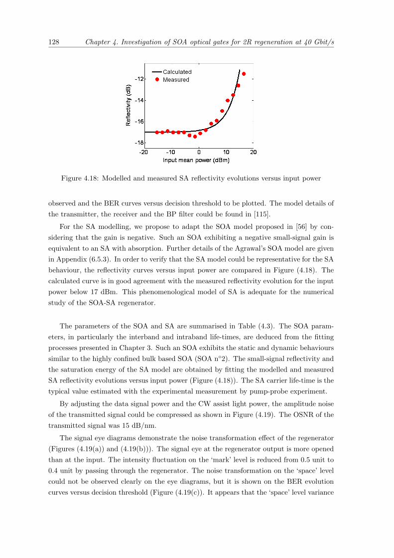
128 Chapter 4. Investigation of SOA optical gates for 2R regeneration at 40 Gbit/s
Figure 4.18: Modelled and measured SA reflectivity evolutions versus input power
observed and the BER curves versus decision threshold to be plotted. The model details of
the transmitter, the receiver and the BP filter could be found in [115].
For the SA modelling, we propose to adapt the SOA model proposed in [56] by con-
sidering that the gain is negative. Such an SOA exhibiting a negative small-signal gain is
equivalent to an SA with absorption. Further details of the Agrawal’s SOA model are given
in Appendix (6.5.3). In order to verify that the SA model could be representative for the SA
behaviour, the reflectivity curves versus input power are compared in Figure (4.18). The
calculated curve is in good agreement with the measured reflectivity evolution for the input
power below 17 dBm. This phenomenological model of SA is adequate for the numerical
study of the SOA-SA regenerator.
The parameters of the SOA and SA are summarised in Table (4.3). The SOA param-
eters, in particularly the interband and intraband life-times, are deduced from the fitting
processes presented in Chapter 3. Such an SOA exhibits the static and dynamic behaviours
similar to the highly confined bulk based SOA (SOA n◦2). The small-signal reflectivity and
the saturation energy of the SA model are obtained by fitting the modelled and measured
SA reflectivity evolutions versus input power (Figure (4.18)). The SA carrier life-time is the
typical value estimated with the experimental measurement by pump-probe experiment.
By adjusting the data signal power and the CW assist light power, the amplitude noise
of the transmitted signal could be compressed as shown in Figure (4.19). The OSNR of the
transmitted signal was 15 dB/nm.
The signal eye diagrams demonstrate the noise transformation effect of the regenerator
(Figures (4.19(a)) and (4.19(b))). The signal eye at the regenerator output is more opened
than at the input. The intensity fluctuation on the ‘mark’ level is reduced from 0.5 unit to
0.4 unit by passing through the regenerator. The noise transformation on the ‘space’ level
could not be observed clearly on the eye diagrams, but it is shown on the BER evolution
curves versus decision threshold (Figure (4.19(c)). It appears that the ‘space’ level variance
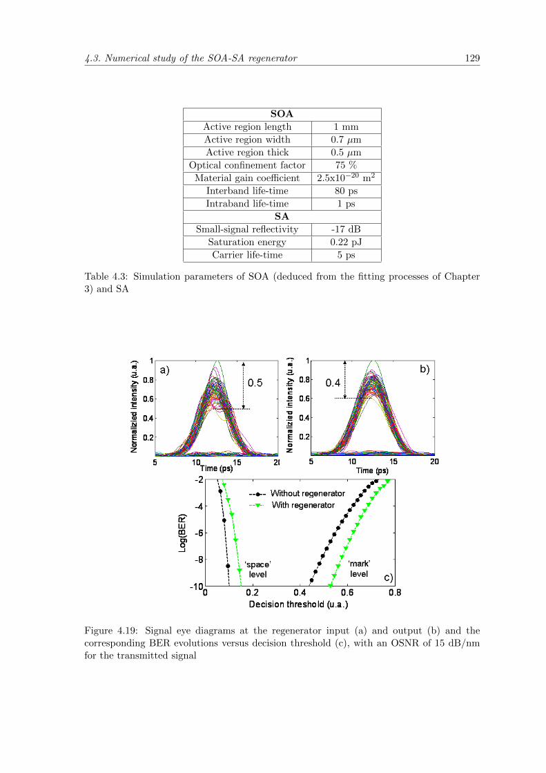
4.3. Numerical study of the SOA-SA regenerator 129
SOA
Active region length 1 mm
Active region width 0.7 µm
Active region thick 0.5 µm
Optical confinement factor 75 %
Material gain coefficient 2.5x10⁻²⁰ m2
Interband life-time 80 ps
Intraband life-time 1 ps
SA
Small-signal reflectivity -17 dB
Saturation energy 0.22 pJ
Carrier life-time 5 ps
Table 4.3: Simulation parameters of SOA (deduced from the fitting processes of Chapter3) and SA
Figure 4.19: Signal eye diagrams at the regenerator input (a) and output (b) and thecorresponding BER evolutions versus decision threshold (c), with an OSNR of 15 dB/nmfor the transmitted signal
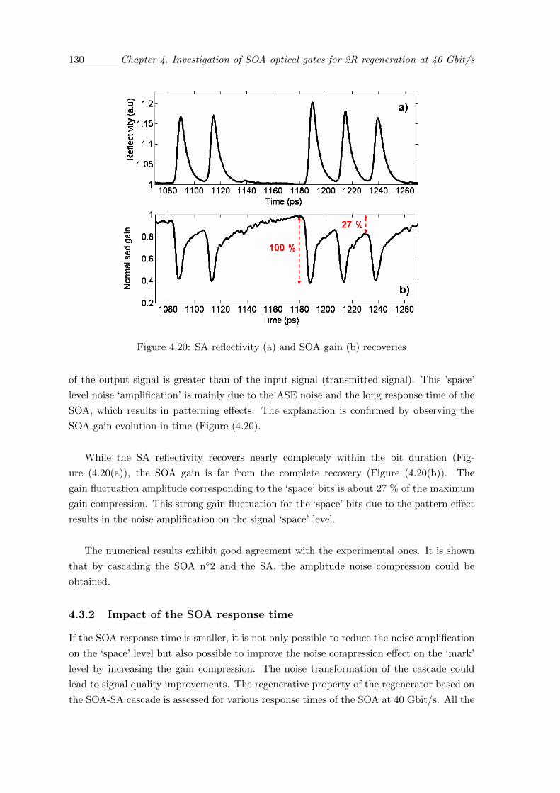
130 Chapter 4. Investigation of SOA optical gates for 2R regeneration at 40 Gbit/s
Figure 4.20: SA reflectivity (a) and SOA gain (b) recoveries
of the output signal is greater than of the input signal (transmitted signal). This ’space’
level noise ‘amplification’ is mainly due to the ASE noise and the long response time of the
SOA, which results in patterning effects. The explanation is confirmed by observing the
SOA gain evolution in time (Figure (4.20).
While the SA reflectivity recovers nearly completely within the bit duration (Fig-
ure (4.20(a)), the SOA gain is far from the complete recovery (Figure (4.20(b)). The
gain fluctuation amplitude corresponding to the ‘space’ bits is about 27 % of the maximum
gain compression. This strong gain fluctuation for the ‘space’ bits due to the pattern effect
results in the noise amplification on the signal ‘space’ level.
The numerical results exhibit good agreement with the experimental ones. It is shown
that by cascading the SOA n◦2 and the SA, the amplitude noise compression could be
obtained.
4.3.2 Impact of the SOA response time
If the SOA response time is smaller, it is not only possible to reduce the noise amplification
on the ‘space’ level but also possible to improve the noise compression effect on the ‘mark’
level by increasing the gain compression. The noise transformation of the cascade could
lead to signal quality improvements. The regenerative property of the regenerator based on
the SOA-SA cascade is assessed for various response times of the SOA at 40 Gbit/s. All the
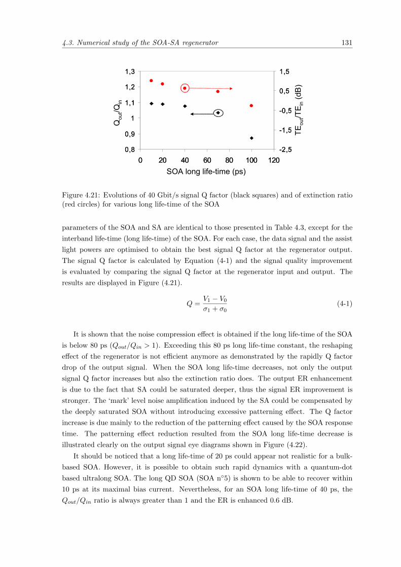
4.3. Numerical study of the SOA-SA regenerator 131
0,8
0,9
1
1,1
1,2
1,3
0 20 40 60 80 100 120SOA response time (ps)
Qou
t/Qin
-2,5
-1,5
-0,5
0,5
1,5
SOA long life-time (ps)
Qou
t/Qin
TEou
t/TE i
n(d
B)
0,8
0,9
1
1,1
1,2
1,3
0 20 40 60 80 100 120SOA response time (ps)
Qou
t/Qin
-2,5
-1,5
-0,5
0,5
1,5
SOA long life-time (ps)
Qou
t/Qin
TEou
t/TE i
n(d
B)
Figure 4.21: Evolutions of 40 Gbit/s signal Q factor (black squares) and of extinction ratio(red circles) for various long life-time of the SOA
parameters of the SOA and SA are identical to those presented in Table 4.3, except for the
interband life-time (long life-time) of the SOA. For each case, the data signal and the assist
light powers are optimised to obtain the best signal Q factor at the regenerator output.
The signal Q factor is calculated by Equation (4-1) and the signal quality improvement
is evaluated by comparing the signal Q factor at the regenerator input and output. The
results are displayed in Figure (4.21).
Q =V1 − V0σ1 + σ0
(4-1)
It is shown that the noise compression effect is obtained if the long life-time of the SOA
is below 80 ps (Qout/Qin > 1). Exceeding this 80 ps long life-time constant, the reshaping
effect of the regenerator is not efficient anymore as demonstrated by the rapidly Q factor
drop of the output signal. When the SOA long life-time decreases, not only the output
signal Q factor increases but also the extinction ratio does. The output ER enhancement
is due to the fact that SA could be saturated deeper, thus the signal ER improvement is
stronger. The ‘mark’ level noise amplification induced by the SA could be compensated by
the deeply saturated SOA without introducing excessive patterning effect. The Q factor
increase is due mainly to the reduction of the patterning effect caused by the SOA response
time. The patterning effect reduction resulted from the SOA long life-time decrease is
illustrated clearly on the output signal eye diagrams shown in Figure (4.22).
It should be noticed that a long life-time of 20 ps could appear not realistic for a bulk-
based SOA. However, it is possible to obtain such rapid dynamics with a quantum-dot
based ultralong SOA. The long QD SOA (SOA n◦5) is shown to be able to recover within
10 ps at its maximal bias current. Nevertheless, for an SOA long life-time of 40 ps, the
Qout/Qin ratio is always greater than 1 and the ER is enhanced 0.6 dB.
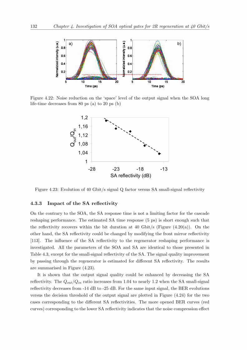
132 Chapter 4. Investigation of SOA optical gates for 2R regeneration at 40 Gbit/s
Figure 4.22: Noise reduction on the ‘space’ level of the output signal when the SOA longlife-time decreases from 80 ps (a) to 20 ps (b)
1
1,04
1,08
1,12
1,16
1,2
-28 -23 -18 -13SA absorption (dB)
Qou
t/Qin
Qou
t/Qin
SA reflectivity (dB)
1
1,04
1,08
1,12
1,16
1,2
-28 -23 -18 -13SA absorption (dB)
Qou
t/Qin
Qou
t/Qin
1
1,04
1,08
1,12
1,16
1,2
-28 -23 -18 -13SA absorption (dB)
Qou
t/Qin
Qou
t/Qin
SA reflectivity (dB)
Figure 4.23: Evolution of 40 Gbit/s signal Q factor versus SA small-signal reflectivity
4.3.3 Impact of the SA reflectivity
On the contrary to the SOA, the SA response time is not a limiting factor for the cascade
reshaping performance. The estimated SA time response (5 ps) is short enough such that
the reflectivity recovers within the bit duration at 40 Gbit/s (Figure (4.20(a)). On the
other hand, the SA reflectivity could be changed by modifying the front mirror reflectivity
[113]. The influence of the SA reflectivity to the regenerator reshaping performance is
investigated. All the parameters of the SOA and SA are identical to those presented in
Table 4.3, except for the small-signal reflectivity of the SA. The signal quality improvement
by passing through the regenerator is estimated for different SA reflectivity. The results
are summarised in Figure (4.23).
It is shown that the output signal quality could be enhanced by decreasing the SA
reflectivity. The Qout/Qin ratio increases from 1.04 to nearly 1.2 when the SA small-signal
reflectivity decreases from -14 dB to -25 dB. For the same input signal, the BER evolutions
versus the decision threshold of the output signal are plotted in Figure (4.24) for the two
cases corresponding to the different SA reflectivities. The more opened BER curves (red
curves) corresponding to the lower SA reflectivity indicates that the noise compression effect
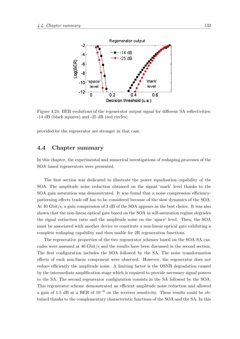
4.4. Chapter summary 133
Figure 4.24: BER evolutions of the regenerator output signal for different SA reflectivities:-14 dB (black squares) and -25 dB (red circles)
provided by the regenerator are stronger in that case.
4.4 Chapter summary
In this chapter, the experimental and numerical investigations of reshaping processes of the
SOA based regenerators were presented.
The first section was dedicated to illustrate the power equalisation capability of the
SOA. The amplitude noise reduction obtained on the signal ‘mark’ level thanks to the
SOA gain saturation was demonstrated. It was found that a noise compression efficiency-
patterning effects trade-off has to be considered because of the slow dynamics of the SOA.
At 40 Gbit/s, a gain compression of 3 dB of the SOA appears as the best choice. It was also
shown that the non-linear optical gate based on the SOA in self-saturation regime degrades
the signal extinction ratio and the amplitude noise on the ‘space’ level. Then, the SOA
must be associated with another device to constitute a non-linear optical gate exhibiting a
complete reshaping capability and then usable for 2R regeneration functions.
The regenerative properties of the two regenerator schemes based on the SOA-SA cas-
cades were assessed at 40 Gbit/s and the results have been discussed in the second section.
The first configuration includes the SOA followed by the SA. The noise transformation
effects of each non-linear component were observed. However, the regenerator does not
reduce efficiently the amplitude noise. A limiting factor is the OSNR degradation caused
by the intermediate amplification stage which is required to provide necessary signal powers
to the SA. The second regenerator configuration consists in the SA followed by the SOA.
This regenerator scheme demonstrated an efficient amplitude noise reduction and allowed
a gain of 1.5 dB at a BER of 10−9 on the receiver sensitivity. These results could be ob-
tained thanks to the complementary characteristic functions of the SOA and the SA. In this
134 Chapter 4. Investigation of SOA optical gates for 2R regeneration at 40 Gbit/s
case, the SOA was placed at the second position of the cascade and thus no intermediate
amplification stage was necessary because the SOA does not require high input signal pow-
ers. Indeed, the regenerator based on the SA followed by the SOA exhibit the reshaping
capability for 2R regeneration functions. This scheme is an integrable solution with a low
energy consumption. The signal wavelength preservation is also one of its main advantages.
The numerical study presented in the third section confirms the regenerative property
of the regenerator scheme based on SOA-SA cascade. The numerical investigation demon-
strated that if the SOA long life-time could be shortened, both quality factor and extinction
ratio of the output signal could be improved. On the other words, the reshaping capability
of the regenerator could be enhanced. Concerning the SA, an increase of the small-signal
reflectivity could lead also to more efficient noise compression of the regenerator.
There are still some challenges for this 2R regenerator solution. The proposed regenera-
tor scheme does not provide a significant ER improvement. And the other challenge may be
the operating bit rate increase. The main factor limiting the SA-SOA cascade operations at
bit rates higher than 40 Gbit/s is the long gain recovery time of the SOA. This response time
is in order of 20 ps. Operations of this regenerator scheme at 160 Gbit/s will not be possible.
Otherwise, the SA response time (5 ps) is even shorter than the bit duration (6.3 ps) at
160 Gbit/s. It could be associated with the long QD SOAs to provide promising solutions at
this data rate. We remind that the long QD SOA exhibit faster gain dynamics than the bulk
SOA used in these experiments. The effective gain recovery time was demonstrated as short
as 3 ps when the filter following the SOA was slightly blue shifted. Moreover, QD SOAs
promise lower gain phase couplings [116] compared to bulk based SOAs. This indicates that
the additional chirp induced by the SOA, and thus the signal spectrum deformation, can
be decreased by using QD structures. Some efforts still have to be made on the long QD
SOA to reduce its gain ripple levels and to make the noise compression experiment possible.
At last, it should be noted that the noise compression capability of the regenerator was
assessed only in back-to-back experiments. Further investigations should be considered to
demonstrate that the regenerator performance is sufficient to maintain signal quality over
long distances by preventing from noise and distortion accumulation. To ensure the SOA-
SA cascade will constitute a good regenerator, it has to be assessed in re-circulating loop
experiments to illustrate its efficiency in a transmission link and its cascadability. In par-
ticular, the signal spectrum deformation shown in Paragraph 4.2.4 may cause impairments
to the signal quality when accumulating after long transmission fibre links.

Part II
All-Optical Clock Recovery

Introduction on all-optical clock
recovery
As discussed in the first chapter, the transmitted optical signal suffers not only from ran-
dom intensity fluctuations but also from random deviation of pulse position during the
propagation. The 3R regeneration is elaborated to overcome all these signal degradations
by associating a 2R device with a retiming function. 3R regenerators with retiming capa-
bility require clock extraction from the incoming data signal. The capacity demand growth
of optical networks is irresistible and will reache electronic limitations. Semiconductor all-
optical 3R regenerators promise ultra-high bit rate operation, full integration possibility and
power consumption reduction. They are therefore an attractive choice to relieve physical
limitations, to improve the transmission distance and to achieve better performance/cost
trade-off. Furthermore, all-optical solutions offer a transparency for the optical networks.
All-Optical Clock Recovery (OCR) is one of principal sub-functions of a full all-optical 3R
regenerator.
The Clock Recovery (CR) function is well known in the electronic domain. Electrical
CRs are usually based on a filter combined with a phase-locked loop. Nowadays, the elec-
tronic CR is well mastered up to the bit rate of 40 Gbit/s. In the last recent years, strong
efforts were made to develop all-optical CR functions which promise a lower cost, a higher
integration capacity and a better network transparency. In a 3R regenerator, the CR task
is to emit an optical pulse stream. It has to be synchronised to the incoming data stream
and match the demands for transmission over the next fibre link. High performance of
all-optical CR was successfully demonstrated at 40 Gbit/s [117], [118] and at 160 Gbit/s
for demultiplexing in OTDM system [119].
This second part of the manuscript is dedicated to the study of all-optical clock re-
covery solutions based on self-pulsating semiconductor lasers. These CR devices could be
associated with a 2R optical non-linear gate to constitute a 3R regenerator. The presented
work is also a part of the French national project ROTOR. The project’s principal goal
was to demonstrate the feasibility of simple and robust all-optical CRs operating at the bit
rate of 43 Gbit/s. Thanks to the collaboration within the project, we could benefit from
two Self-Pulsating (SP) lasers based on bulk and quantum-dot materials fabricated by our
138 Introduction on all-optical clock recovery
partner: Alcatel-Lucent Thales III-V Lab.
Chapter 5 introduces firstly the different roles of CR function in transmission systems.
All-optical clock recovery based on self-pulsating semiconductor lasers is then described in
detail. The principle of the clock recovery technique is presented. At last, its advantages
and limitations are discussed.
The first section of Chapter 6 presents the characterisation and performance evaluation
of a clock recovery through different aspects. In this section, we present for the first time a
novel characterisation technique called remodulation. This original experiment developed in
our laboratory allowed studies on various OCR configurations [120], [121], [13], [122], [123],
[124]. Most of studies on OCR functions in the thesis exploit this original characterisation
scheme which is suitable for regeneration applications.
A performance comparison of OCR devices based on a bulk and a quantum-dot SP lasers
has been carried out. The results are presented in Section 6.2. In Section 6.3, a solution
consisting in using of a pre-filtering stage in front of the bulk-SP laser was proposed in order
to improve the recovered clock quality. The performance enhancement is demonstrated via
bit error rate measurements. In Section 6.4, the polarisation sensitivity assessment of
different OCRs is investigated. At last, a primary study on OCR resistance to Polarisation
Mode Dispersion is reported in Section 6.5.
Chapter 5
All-optical clock recovery for 3R
regeneration
5.1 Clock recovery
In optical networks, clock recovery is a key function among the functional blocks such
as receiver, in-line repeaters and demultiplexers in future OTDM systems. The role of
the Clock Recovery (CR) function in these elements is extracting a stable clock which is
synchronised (in frequency and in phase) to the incoming data signal and ideally with a
minimal timing jitter.
5.1.1 Role of clock recovery function in optical networks
In a receiver, CRs provide a time reference to the flip-flop decision gate. Decision of value
0 or 1 of a bit is made at an accurate moment. The decisions have to be done in a
regular rhythm, and duration between two successive decisions has to be equal to the bit
duration. If the repetition rates of the data signal and of the flip-flop clock are different,
the decision moment slips step by step far away from the optimal sampling time. This
deviation introduces errors and the detection gives false information. Therefore the clock
which is used for receiver time reference must be derived accurately from the received signal
itself.
In future OTDM systems, temporal demultiplexing requires a CR to extract a base
rate clock B/N from a transmitted OTDM data signal which is at a line rate B. The
demultiplexing function allows isolating each base data stream from N interleaved streams
in the data flow. For example, it is possible to extract a 40 GHz clock from an OTDM
signal at bit rates of 160 Gbit/s and 320 Gbit/s [125], [126]. The CR must provide a
low timing jitter clock which is synchronised to the incoming data signal. Afterwards, the
recovered clock is distributed to demultiplexers, routers, channel selectors, and receivers. In
OTDM systems, the aggregate data rate exceeds the state-of-the-art speed limit of electronic
components, all-optical CR offers a novel solution to provide retiming signals and perform
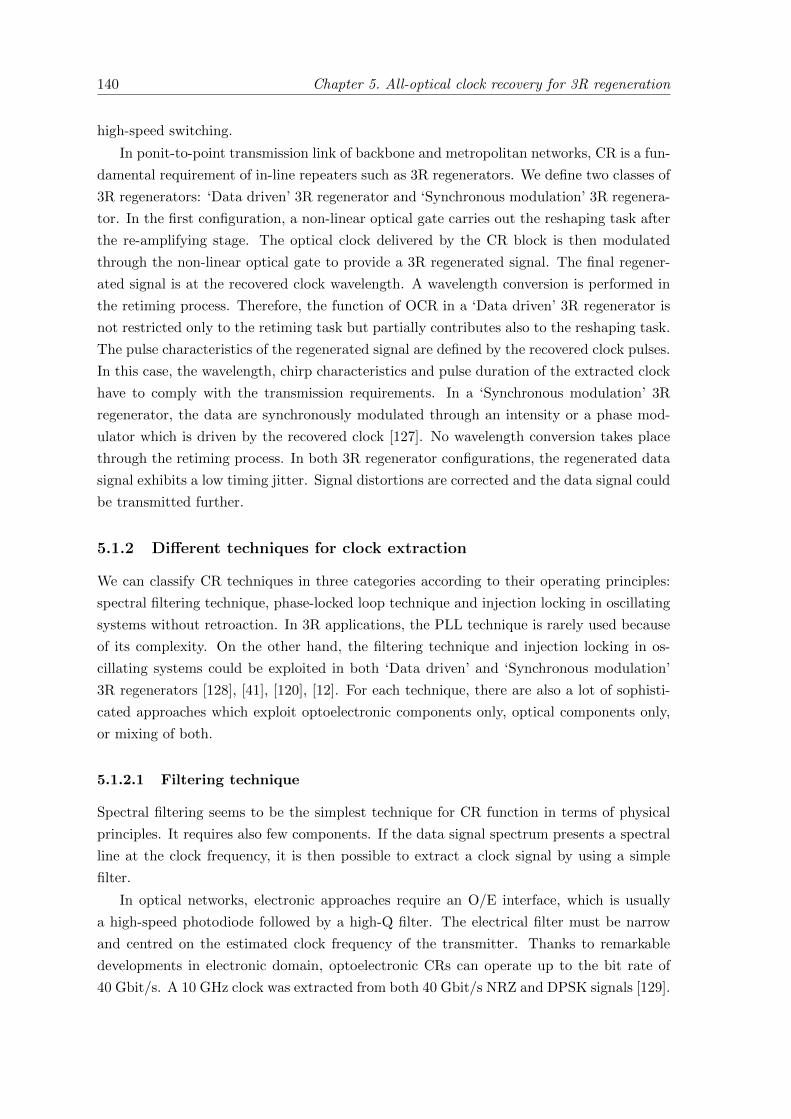
140 Chapter 5. All-optical clock recovery for 3R regeneration
high-speed switching.
In ponit-to-point transmission link of backbone and metropolitan networks, CR is a fun-
damental requirement of in-line repeaters such as 3R regenerators. We define two classes of
3R regenerators: ‘Data driven’ 3R regenerator and ‘Synchronous modulation’ 3R regenera-
tor. In the first configuration, a non-linear optical gate carries out the reshaping task after
the re-amplifying stage. The optical clock delivered by the CR block is then modulated
through the non-linear optical gate to provide a 3R regenerated signal. The final regener-
ated signal is at the recovered clock wavelength. A wavelength conversion is performed in
the retiming process. Therefore, the function of OCR in a ‘Data driven’ 3R regenerator is
not restricted only to the retiming task but partially contributes also to the reshaping task.
The pulse characteristics of the regenerated signal are defined by the recovered clock pulses.
In this case, the wavelength, chirp characteristics and pulse duration of the extracted clock
have to comply with the transmission requirements. In a ‘Synchronous modulation’ 3R
regenerator, the data are synchronously modulated through an intensity or a phase mod-
ulator which is driven by the recovered clock [127]. No wavelength conversion takes place
through the retiming process. In both 3R regenerator configurations, the regenerated data
signal exhibits a low timing jitter. Signal distortions are corrected and the data signal could
be transmitted further.
5.1.2 Different techniques for clock extraction
We can classify CR techniques in three categories according to their operating principles:
spectral filtering technique, phase-locked loop technique and injection locking in oscillating
systems without retroaction. In 3R applications, the PLL technique is rarely used because
of its complexity. On the other hand, the filtering technique and injection locking in os-
cillating systems could be exploited in both ‘Data driven’ and ‘Synchronous modulation’
3R regenerators [128], [41], [120], [12]. For each technique, there are also a lot of sophisti-
cated approaches which exploit optoelectronic components only, optical components only,
or mixing of both.
5.1.2.1 Filtering technique
Spectral filtering seems to be the simplest technique for CR function in terms of physical
principles. It requires also few components. If the data signal spectrum presents a spectral
line at the clock frequency, it is then possible to extract a clock signal by using a simple
filter.
In optical networks, electronic approaches require an O/E interface, which is usually
a high-speed photodiode followed by a high-Q filter. The electrical filter must be narrow
and centred on the estimated clock frequency of the transmitter. Thanks to remarkable
developments in electronic domain, optoelectronic CRs can operate up to the bit rate of
40 Gbit/s. A 10 GHz clock was extracted from both 40 Gbit/s NRZ and DPSK signals [129].
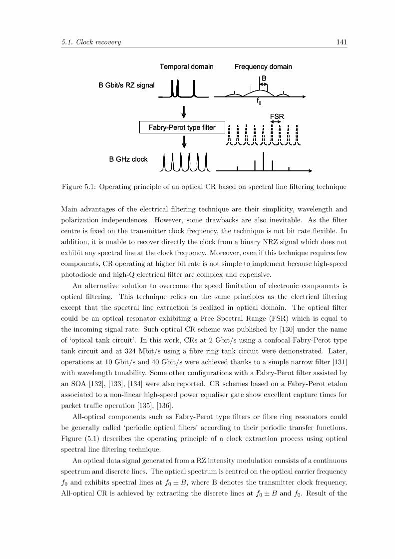
5.1. Clock recovery 141
B
FSR
Frequency domain
B Gbit/s RZ signal
f0
Temporal domain
Fabry-Perot type filter
B GHz clock
B
FSR
Frequency domain
B Gbit/s RZ signal
f0
Temporal domain
Fabry-Perot type filter
B GHz clock
Figure 5.1: Operating principle of an optical CR based on spectral line filtering technique
Main advantages of the electrical filtering technique are their simplicity, wavelength and
polarization independences. However, some drawbacks are also inevitable. As the filter
centre is fixed on the transmitter clock frequency, the technique is not bit rate flexible. In
addition, it is unable to recover directly the clock from a binary NRZ signal which does not
exhibit any spectral line at the clock frequency. Moreover, even if this technique requires few
components, CR operating at higher bit rate is not simple to implement because high-speed
photodiode and high-Q electrical filter are complex and expensive.
An alternative solution to overcome the speed limitation of electronic components is
optical filtering. This technique relies on the same principles as the electrical filtering
except that the spectral line extraction is realized in optical domain. The optical filter
could be an optical resonator exhibiting a Free Spectral Range (FSR) which is equal to
the incoming signal rate. Such optical CR scheme was published by [130] under the name
of ‘optical tank circuit’. In this work, CRs at 2 Gbit/s using a confocal Fabry-Perot type
tank circuit and at 324 Mbit/s using a fibre ring tank circuit were demonstrated. Later,
operations at 10 Gbit/s and 40 Gbit/s were achieved thanks to a simple narrow filter [131]
with wavelength tunability. Some other configurations with a Fabry-Perot filter assisted by
an SOA [132], [133], [134] were also reported. CR schemes based on a Fabry-Perot etalon
associated to a non-linear high-speed power equaliser gate show excellent capture times for
packet traffic operation [135], [136].
All-optical components such as Fabry-Perot type filters or fibre ring resonators could
be generally called ‘periodic optical filters’ according to their periodic transfer functions.
Figure (5.1) describes the operating principle of a clock extraction process using optical
spectral line filtering technique.
An optical data signal generated from a RZ intensity modulation consists of a continuous
spectrum and discrete lines. The optical spectrum is centred on the optical carrier frequency
f0 and exhibits spectral lines at f0 ± B, where B denotes the transmitter clock frequency.
All-optical CR is achieved by extracting the discrete lines at f0 ± B and f0. Result of the
142 Chapter 5. All-optical clock recovery for 3R regeneration
Amplifier
VCO Filter
Optical signal
Optical or electricalclock Control
Phasecomparator
O/EInterface
AmplifierAmplifier
VCOVCO FilterFilter
Optical signal
Optical or electricalclock Control
Phasecomparator
O/EInterface
Figure 5.2: Basic structure of a conventinal phase-locked loop for CR
filtering process is an optical clock at the same wavelength as the incoming optical signal
and at the same frequency as the transmitter clock. The three following conditions have to
be satisfied: one of the filter resonance peaks superimposes on the optical carrier frequency,
the optical filter FSR is equal to the transmitter clock rate and the optical carrier linewidth
is narrower than the resonator bandwidth.
The first advantage of the optical solution is the transparency for optical networks. The
second advantage is that optical CRs allow operation at ultrahigh bit rates which could not
be achieved by using only optoelectronic components. This high-speed operation possibility
results from the nature of the key component: optical filters.
In a CR based on optical filtering, the frequency drift of a resonance peak away from the
optical carrier and filter finesse are crucial parameters which determine the CR performance.
Thus, main limiting factor of the optical filtering technique is the requirement of high
finesse filters. Besides, the technique suffers also from strong wavelength, polarisation and
sequence length dependences [137]. Wavelength dispersion which causes irregular resonance
peak intervals and temperature regulation should be also taken into account.
At last, the first CR scheme based on optical spectral filtering operating with multi-
channels and at multi-rates should be referred [138]. The CR scheme consists of a bire-
fringent resonator and a polarizer. Proof-of-principle experiment was demonstrated for 21
simultaneous channels including 20 data streams at 10 Gbit/s and one at 40 Gbit/s. This
solution opens a promising alternative for dense WDM parallel-optical signal processing.
5.1.2.2 Phase-locked loop technique
Phase-locked loop (PLL) is also largely used for CR function thanks to its reliability. A
PLL allows modulation frequency extraction from a data signal. In general, a PLL consists
of a phase comparator, an amplifier, a filter and a local voltage-controlled oscillator (VCO).
The basic structure of a conventional PLL is shown in Figure (5.2). When the input data
stream is an optical signal, an O/E interface is necessary and it is usually a fast photodiode.
The electrical signal delivered by the photodiode is then injected to the phase comparator.
The basic idea is that the electrical signal delivered by the photodiode beats with the
5.1. Clock recovery 143
low-rate clock signal delivered by the local oscillator through the high-speed phase com-
parator. The produced signal is a slowly varying signal which is proportional to the phase
difference between the local clock and data stream. This signal is then fed back (after
having been amplified and filtered) to the VCO. The retroaction allows locking the VCO
in phase with the incoming signal clock. In general, parameters of amplification and filter-
ing stages determine the loop operating range, the locking characteristics and the residual
phase mismatch between input and output signals. The PLL speed is determined mainly by
the photodiode and the phase comparator. A CR based on a PLL using entirely electronic
components was successfully demonstrated for 10 GHz clock extraction at an ultrahigh bit
rate of 100 Gbit/s [139].
To achieve higher bit rates, speed limitation of O/E interface and especially of the elec-
trical phase comparator can be overcome by using optical phase comparators. Response
times of non-linear optical processes usually used in phase comparators are much shorter
than those of electrical processes. There is a huge number of optical and optoelectronic PLL
configurations. The most considered optical components in PLL based CRs are ElectroAb-
sorption Modulators (EAM), Semiconductor Optical Amplifiers (SOA) and also Lithium
Niobate waveguides [140]. These components could be used as O/E interfaces or/and as
ultrahigh-speed phase comparators. PLLs using EAM as phase comparator allowed reali-
sation of a CR operating at 160 Gbit/s [141] and up to 320 Gbit/s [125]. Both experiments
reported excellent timing jitters below 300 fs. SOA based PLLs offer a lot of sophisticated
CR schemes [142], [143], [144], [126]. Most of them exploit four-wave-mixing process, cross
gain and cross phase modulations and interferometric configurations. A SOA based PLL
allowed to recover clock for a 640 Gbit/s lab transmission and a 320 Gbit/s field trial
transmission with high timing jitter performance [126].
CR processes based on PLLs are well known for their high stability and high recovered
clock quality characterised by sub picoseconds timing jitters. Jitter values below 300 fs (in
the frequency range from 100 Hz to 10 MHz) are currently obtained with CRs using the
PLL technique [143], [145], [140], [126]. Beside these advantages, complexity is considered
as the greatest drawback of the technique. Moreover, PLL based CR functions require in
general a long time for synchronization to the data stream. This last inconvenient make
them not suitable for short optical packet traffic.
5.1.2.3 Injection locking in oscillating systems without retroaction
Another solution for CR function is using oscillating systems which could be synchronized to
an injected optical signal without retroaction. Energy injection from an external source into
an oscillator can lock the last one onto the referent source. This synchronization capability
of oscillators has been largely studied in electronics and recently extensively investigated in
the optical domain. The goals are not only the deployment of broadband wireless technology
but also the bit rate rising in long and ultralong haul transmissions. Oscillating systems
144 Chapter 5. All-optical clock recovery for 3R regeneration
consist of electronic or optical components or both.
Among electronic components, heterojunction bipolar phototransistor should be con-
sidered a good candidate. A CR consisting in direct optical signal injection into a self-
oscillating phototransistor was proposed [146]. In this work, a 10 GHz electrical clock was
extracted from 10 Gbit/s and 40 Gbit/s signals. Error-free performance at 10 Gbit/s could
be achieved. EAM based ring resonator is another solution which offers compact and stable
CR devices with integration possibility. Operation at bit rate of 40 Gbit/s was also demon-
strated [147]. However, the reported timing jitter of about 500 fs is a poor performance in
comparison to the state-of-the-art of CR devices.
Among optical oscillating systems for CR, leading roles should be distributed to SP
multi-sections lasers [148], [149], [117] and mode locked lasers [150], [151], [118]. The pul-
sating frequency of these lasers could be locked by injecting an optical data stream. The
injected signal rate must be nearby the free pulsating frequency of the laser or a multi-
ple of this frequency. Some CR schemes using mode-locked fibre ring lasers were inves-
tigated [152], [153], [154] and ultrahigh-speed operation at 160 Gbit/s was achieved [155].
Simultaneous CR of several WDM channels at 10 Gbit/s was successfully demonstrated [156]
by using a CR module in actively-mode-locked fibre ring laser configuration.
OCR schemes using fibre ring lasers can give high intensity pulse streams and large
wavelength tuning ranges for the incoming data signal [154] Polarisation insensitive circuit
could be also obtained with the fibre ring laser approach. On the other hand, the timing
jitter of the recovered clock could be easily degraded by environmental perturbations along
the fibre cavity length. Cavity stabilisation was investigated to resolve this problem [153]
but the complex stabilisation circuit is an obstacle for applications in real communication
systems. Another CR based on the fibre ring laser demonstrated good performances: oper-
ation at ultrahigh bit rate of 160 Gbit/s, locking range of 5 MHz and recovered clock timing
jitter below 200 fs [155]. However, this timing jitter could be achieved only with assistance
of a post electrical signal processing. Therefore, the transparency is not assured and this
solution is not an appropriate option for all-optical 3R regeneration applications.
In the context of CR development for all-optical 3R regenerators, SP multi-sections
lasers and mode locked lasers based on semiconductor technology appears as the most
promising candidates. Integration potential, simple deployment and high bit rate operation
are indisputable virtues of CR functions using semiconductor lasers. Operating principle,
advantages and also challenges of all-optical CR devices using this technology are presented
in Section 5.2.
5.2 Solution based on self-pulsating semiconductor lasers
All-optical clock recoveries based on SP semiconductor lasers attract firstly for their in-
tegration potential, low power consumption and deployment simplicity for full optical 3R
regeneration applications.
5.2. Solution based on self-pulsating semiconductor lasers 145
5.2.1 Operation principle
Self-pulsations have been observed in various laser types such as Fabry-Perot, DFB, and
DBR lasers. These lasers provide optical power which varies spontaneously and periodically
without bias current modulation. They are so called self-pulsating lasers. The self-pulsation
results from the laser dynamics. In a simple view, if two oscillating modes of the cavity
exhibit close threshold gains, a mode competition is then established. In the active region,
beating of the two modes is produced at the frequency which corresponds to the frequency
difference. Gain and index of the active region are then modulated at this beating rate and
the modulation result in self-pulsation. An optical clock signal is produced. At high beating
frequencies (upper 100 GHz), the self-pulsation phenomenon could not be explained only
by the dynamics of intraband effects any more. But the four-wave-mixing (FWM) should
be also considered.
It is demonstrated that injection of a modulated optical signal into a SP laser can lead to
a synchronisation of the generated clock to the injected signal. Locking mechanism relies on
gain and index modulations created by the external optical signal within the active region.
If the gain spectrum is homogeneously broadened, then the gain of each mode is modulated
exactly at the same frequency. Modulation spectral lines of each mode appear. If the clock
frequency of the injected signal is equal to the laser Free Spectral Range (FSR) then the
modulation lines and the laser longitudinal modes overlay and synchronisation takes place.
Operation of an OCR scheme based on SP laser is described in Figure (5.3).
Simple OCR device could be constituted of a SP laser, an optical circulator (OC) and
an optical filter. The incoming data signal is injected into the laser via the OC. The optical
filter is placed at the circulator output to select clock signal generated by the SP laser.
When the SP laser is not synchronised to the incoming data, the OCR is in unlocked
regime. In that case, temporal waveform and electrical spectrum of the detected output
signal take arbitrary forms as shown in Figure (5.3 (a)). No clear pulse stream is observed
on the oscilloscope. The spectral lines at the clock frequency of the data signal and at the
free pulsating frequency of the laser are separated in the electrical spectrum. By adjusting
the operation parameters, the SP laser synchronisation to the incoming data signal could
be achieved and the OCR function is now in locked regime. In that case, the laser emits
an optical clock which is in phase with the injected signal and at the transmitter clock
frequency. In other words, the signal clock is recovered. In general, we observe a clear clock
signal on oscilloscope and only one spectral line in the electrical RF spectrum as shown in
Figure (5.3 (b)) (case of a quantum-dot based SP laser).
5.2.2 Advantages and limitations
Besides integration potential, low power consumption, deployment simplicity and high bit
rate operation, OCR devices based on SP semiconductor lasers attract also a lot of in-
vestigations for other interesting features: pulsation frequency tuning possibility, ultrafast
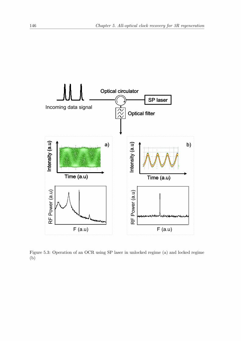
146 Chapter 5. All-optical clock recovery for 3R regeneration
Optical circulator
Optical filter
SP laserIncoming data signal
F (a.u)
RF
Pow
er (a
.u)
Inte
nsity
(a.u
)
Time (a.u)
a)
RF
Pow
er (a
.u)
F (a.u)
Inte
nsity
(a.u
)
Time (a.u)
b)
Optical circulator
Optical filter
SP laserIncoming data signal
Optical circulator
Optical filter
SP laserIncoming data signal
F (a.u)
RF
Pow
er (a
.u)
F (a.u)
RF
Pow
er (a
.u)
F (a.u)
RF
Pow
er (a
.u)
Inte
nsity
(a.u
)
Time (a.u)
Inte
nsity
(a.u
)
Time (a.u)
Inte
nsity
(a.u
)
Time (a.u)
a)
RF
Pow
er (a
.u)
F (a.u)
Inte
nsity
(a.u
)
Time (a.u)
Inte
nsity
(a.u
)
Time (a.u)
Inte
nsity
(a.u
)
Time (a.u)
b)
Figure 5.3: Operation of an OCR using SP laser in unlocked regime (a) and locked regime(b)
5.2. Solution based on self-pulsating semiconductor lasers 147
locking and polarisation insensitivity [148], [128], [41].
The first CR function operating at 35 Gbit/s and totally integrated on chip was demon-
strated [157]. An SP laser based CR was performed at 80 Gbit/s with predicted operations
at 160 Gbit/s and even higher [158]. Bit rate flexibility is not available with CRs based
on phase-locked loop or spectral filtering. On the contrary, SP lasers offer continuous fre-
quency tuning possibility via driving DC currents. An SP laser based OCR was reported
by [148] with a frequency range from 3 to 5.2 GHz. This range was enlarged later from 10
to 40 GHz to cover different SDH bit rates [128] and from 25 to 82 GHz [158]. Bit rate
flexible 3R regenerators become possible thanks to optical CR based on SP lasers.
A new challenge for CR functions is arising from the future asynchronous networks. In
such system, clock extraction device has to be able to recover the signal clock packet by
packet. This characteristic leads to requirement of ultrafast synchronisation. Some CR
configurations based on SP lasers were proven compatible with asynchronous packet traffic
thanks to short locking times of few nanoseconds [128], [159]. We remind one more time
that ultrafast synchronisation to asynchronous data packets is a real problem for electronics.
Wavelength and polarization insensitivity will make a CR device ideal for all-optical
3R regeneration. In optical transmission system, the CR function should be operational
independently from the wavelength of the incoming signal. SP laser based CRs can offer
operating wavelength range covering entirely the C band for the incoming optical signal
[149], [160].
At last, a key quality criterion of an OCR device is the timing jitter of the recovered
clock. A lot of technological efforts have been and are carried out to achieve SP lasers de-
livering high quality clock and being compatible with telecommunications standards. RMS
(root-mean square) timing jitters of an extracted clock less than 300 fs were obtained with
SP semiconductor lasers [161], [162]. These results satisfy jitter performance required for
160 Gbit/s operations. New generation of SP lasers based on quantum-dot technology al-
lows new CR perspectives. The first CR function based on a quantum-dot Fabry-Perot
SP laser was reported by [118] at bit rate of 40 Gbit/s. Thanks to high spectral purity
of the quantum-dot laser, CR function exhibits an excellent timing jitter suppression ef-
fect. A jitter reduction from 1.37 ps on the input signal to 310 fs on the recovered clock
was reported. Moreover, another OCR scheme based on the same component type was
demonstrated compatible with multi-data rates operations [13]. Low sensitivity to input
chromatic dispersion and optical noise were also reported [121], [163]. To overcome the
intrinsic polarisation sensitivity of quantum-dot structures, a solution consisting in placing
a bulk based DBR laser in front of the QD laser has been proposed [164]. The tandem
inherits polarisation insensitive characteristic of the bulk laser and the excellent jitter fil-
tering efficiency of the QD laser [164], [123]. This CR scheme was used for a 3R regenerator
in synchronous modulation configuration. Cascadability assessment in re-circulating loop
showed a strong transmission distance enhancement thanks to the retiming function [12].
CR solutions based on oscillating systems are mainly limited by oscillators themselves

148 Chapter 5. All-optical clock recovery for 3R regeneration
because the clock frequency has to be close to their free pulsating frequency (or to multiple
of the SP frequency if the device is able to extract a subharmonic clock). CR devices based
on SP lasers also need a spectral line at the interested frequency in the signal electrical
spectrum. This is a difficulty in clock extraction from a NRZ signal with a simple SP
laser. A pre-processing circuit was developed to be combined with an SP laser based CR.
It consisted of an SOA followed by an optical filter. This scheme allowed clock extraction
from an NRZ signal. Good timing jitter reduction and stable locking at 40 Gbit/s were
obtained with this novel scheme [165].
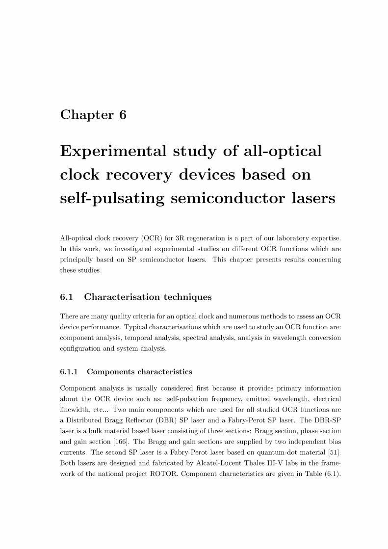
Chapter 6
Experimental study of all-optical
clock recovery devices based on
self-pulsating semiconductor lasers
All-optical clock recovery (OCR) for 3R regeneration is a part of our laboratory expertise.
In this work, we investigated experimental studies on different OCR functions which are
principally based on SP semiconductor lasers. This chapter presents results concerning
these studies.
6.1 Characterisation techniques
There are many quality criteria for an optical clock and numerous methods to assess an OCR
device performance. Typical characterisations which are used to study an OCR function are:
component analysis, temporal analysis, spectral analysis, analysis in wavelength conversion
configuration and system analysis.
6.1.1 Components characteristics
Component analysis is usually considered first because it provides primary information
about the OCR device such as: self-pulsation frequency, emitted wavelength, electrical
linewidth, etc... Two main components which are used for all studied OCR functions are
a Distributed Bragg Reflector (DBR) SP laser and a Fabry-Perot SP laser. The DBR-SP
laser is a bulk material based laser consisting of three sections: Bragg section, phase section
and gain section [166]. The Bragg and gain sections are supplied by two independent bias
currents. The second SP laser is a Fabry-Perot laser based on quantum-dot material [51].
Both lasers are designed and fabricated by Alcatel-Lucent Thales III-V labs in the frame-
work of the national project ROTOR. Component characteristics are given in Table (6.1).
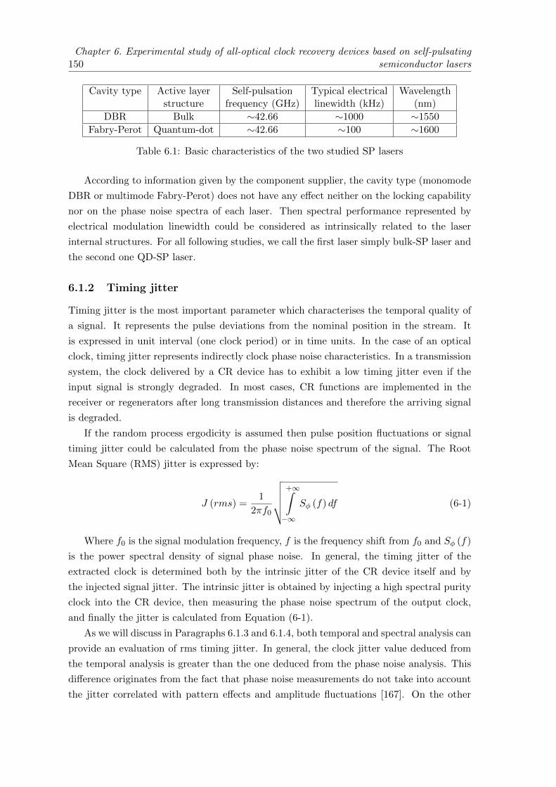
150Chapter 6. Experimental study of all-optical clock recovery devices based on self-pulsating
semiconductor lasers
Cavity type Active layer Self-pulsation Typical electrical Wavelengthstructure frequency (GHz) linewidth (kHz) (nm)
DBR Bulk ∼42.66 ∼1000 ∼1550
Fabry-Perot Quantum-dot ∼42.66 ∼100 ∼1600
Table 6.1: Basic characteristics of the two studied SP lasers
According to information given by the component supplier, the cavity type (monomode
DBR or multimode Fabry-Perot) does not have any effect neither on the locking capability
nor on the phase noise spectra of each laser. Then spectral performance represented by
electrical modulation linewidth could be considered as intrinsically related to the laser
internal structures. For all following studies, we call the first laser simply bulk-SP laser and
the second one QD-SP laser.
6.1.2 Timing jitter
Timing jitter is the most important parameter which characterises the temporal quality of
a signal. It represents the pulse deviations from the nominal position in the stream. It
is expressed in unit interval (one clock period) or in time units. In the case of an optical
clock, timing jitter represents indirectly clock phase noise characteristics. In a transmission
system, the clock delivered by a CR device has to exhibit a low timing jitter even if the
input signal is strongly degraded. In most cases, CR functions are implemented in the
receiver or regenerators after long transmission distances and therefore the arriving signal
is degraded.
If the random process ergodicity is assumed then pulse position fluctuations or signal
timing jitter could be calculated from the phase noise spectrum of the signal. The Root
Mean Square (RMS) jitter is expressed by:
J (rms) =1
2πf0
√√√√√ +∞∫−∞
Sφ (f) df (6-1)
Where f0 is the signal modulation frequency, f is the frequency shift from f0 and Sφ (f)
is the power spectral density of signal phase noise. In general, the timing jitter of the
extracted clock is determined both by the intrinsic jitter of the CR device itself and by
the injected signal jitter. The intrinsic jitter is obtained by injecting a high spectral purity
clock into the CR device, then measuring the phase noise spectrum of the output clock,
and finally the jitter is calculated from Equation (6-1).
As we will discuss in Paragraphs 6.1.3 and 6.1.4, both temporal and spectral analysis can
provide an evaluation of rms timing jitter. In general, the clock jitter value deduced from
the temporal analysis is greater than the one deduced from the phase noise analysis. This
difference originates from the fact that phase noise measurements do not take into account
the jitter correlated with pattern effects and amplitude fluctuations [167]. On the other
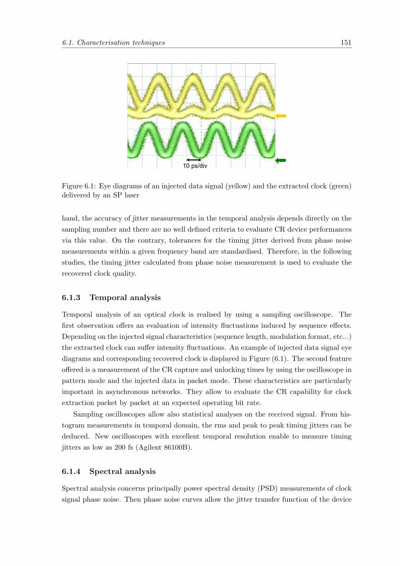
6.1. Characterisation techniques 151
10 ps/div10 ps/div
Figure 6.1: Eye diagrams of an injected data signal (yellow) and the extracted clock (green)delivered by an SP laser
hand, the accuracy of jitter measurements in the temporal analysis depends directly on the
sampling number and there are no well defined criteria to evaluate CR device performances
via this value. On the contrary, tolerances for the timing jitter derived from phase noise
measurements within a given frequency band are standardised. Therefore, in the following
studies, the timing jitter calculated from phase noise measurement is used to evaluate the
recovered clock quality.
6.1.3 Temporal analysis
Temporal analysis of an optical clock is realised by using a sampling oscilloscope. The
first observation offers an evaluation of intensity fluctuations induced by sequence effects.
Depending on the injected signal characteristics (sequence length, modulation format, etc...)
the extracted clock can suffer intensity fluctuations. An example of injected data signal eye
diagrams and corresponding recovered clock is displayed in Figure (6.1). The second feature
offered is a measurement of the CR capture and unlocking times by using the oscilloscope in
pattern mode and the injected data in packet mode. These characteristics are particularly
important in asynchronous networks. They allow to evaluate the CR capability for clock
extraction packet by packet at an expected operating bit rate.
Sampling oscilloscopes allow also statistical analyses on the received signal. From his-
togram measurements in temporal domain, the rms and peak to peak timing jitters can be
deduced. New oscilloscopes with excellent temporal resolution enable to measure timing
jitters as low as 200 fs (Agilent 86100B).
6.1.4 Spectral analysis
Spectral analysis concerns principally power spectral density (PSD) measurements of clock
signal phase noise. Then phase noise curves allow the jitter transfer function of the device
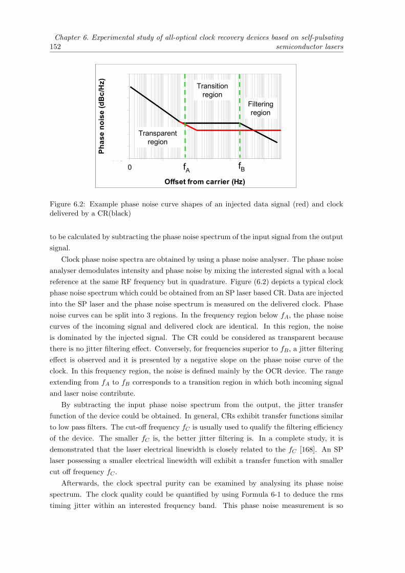
152Chapter 6. Experimental study of all-optical clock recovery devices based on self-pulsating
semiconductor lasers
-140
-120-100
-80-60
-40-20
0
1,E+00 1,E+02 1,E+04 1,E+06 1,E+08
Offset from carrier (Hz)
Phas
e no
ise
(dB
c/H
z)
Transparentregion
Transitionregion
Filteringregion
0 fA fB-140
-120-100
-80-60
-40-20
0
1,E+00 1,E+02 1,E+04 1,E+06 1,E+08
Offset from carrier (Hz)
Phas
e no
ise
(dB
c/H
z)
Transparentregion
Transitionregion
Filteringregion
-140
-120-100
-80-60
-40-20
0
1,E+00 1,E+02 1,E+04 1,E+06 1,E+08
Offset from carrier (Hz)
Phas
e no
ise
(dB
c/H
z)
Transparentregion
Transitionregion
Filteringregion
0 fA fB
Figure 6.2: Example phase noise curve shapes of an injected data signal (red) and clockdelivered by a CR(black)
to be calculated by subtracting the phase noise spectrum of the input signal from the output
signal.
Clock phase noise spectra are obtained by using a phase noise analyser. The phase noise
analyser demodulates intensity and phase noise by mixing the interested signal with a local
reference at the same RF frequency but in quadrature. Figure (6.2) depicts a typical clock
phase noise spectrum which could be obtained from an SP laser based CR. Data are injected
into the SP laser and the phase noise spectrum is measured on the delivered clock. Phase
noise curves can be split into 3 regions. In the frequency region below fA, the phase noise
curves of the incoming signal and delivered clock are identical. In this region, the noise
is dominated by the injected signal. The CR could be considered as transparent because
there is no jitter filtering effect. Conversely, for frequencies superior to fB, a jitter filtering
effect is observed and it is presented by a negative slope on the phase noise curve of the
clock. In this frequency region, the noise is defined mainly by the OCR device. The range
extending from fA to fB corresponds to a transition region in which both incoming signal
and laser noise contribute.
By subtracting the input phase noise spectrum from the output, the jitter transfer
function of the device could be obtained. In general, CRs exhibit transfer functions similar
to low pass filters. The cut-off frequency fC is usually used to qualify the filtering efficiency
of the device. The smaller fC is, the better jitter filtering is. In a complete study, it is
demonstrated that the laser electrical linewidth is closely related to the fC [168]. An SP
laser possessing a smaller electrical linewidth will exhibit a transfer function with smaller
cut off frequency fC .
Afterwards, the clock spectral purity can be examined by analysing its phase noise
spectrum. The clock quality could be quantified by using Formula 6-1 to deduce the rms
timing jitter within an interested frequency band. This phase noise measurement is so
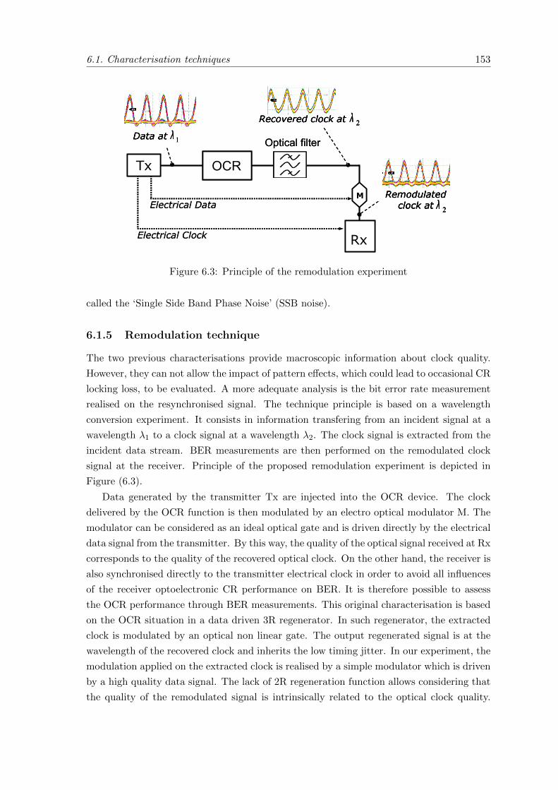
6.1. Characterisation techniques 153
Optical filter
Electrical Data
Electrical Clock
M
Tx
Rx
OCR
Remodulated clock at 2λ
Data at 1λRecovered clock at 2λ
Optical filter
Electrical Data
Electrical Clock
M
Tx
Rx
OCROCR
Remodulated clock at 2λ
Remodulated clock at 2λ
Data at 1λData at 1λRecovered clock at 2λRecovered clock at 2λ
Figure 6.3: Principle of the remodulation experiment
called the ‘Single Side Band Phase Noise’ (SSB noise).
6.1.5 Remodulation technique
The two previous characterisations provide macroscopic information about clock quality.
However, they can not allow the impact of pattern effects, which could lead to occasional CR
locking loss, to be evaluated. A more adequate analysis is the bit error rate measurement
realised on the resynchronised signal. The technique principle is based on a wavelength
conversion experiment. It consists in information transfering from an incident signal at a
wavelength λ1 to a clock signal at a wavelength λ2. The clock signal is extracted from the
incident data stream. BER measurements are then performed on the remodulated clock
signal at the receiver. Principle of the proposed remodulation experiment is depicted in
Figure (6.3).
Data generated by the transmitter Tx are injected into the OCR device. The clock
delivered by the OCR function is then modulated by an electro optical modulator M. The
modulator can be considered as an ideal optical gate and is driven directly by the electrical
data signal from the transmitter. By this way, the quality of the optical signal received at Rx
corresponds to the quality of the recovered optical clock. On the other hand, the receiver is
also synchronised directly to the transmitter electrical clock in order to avoid all influences
of the receiver optoelectronic CR performance on BER. It is therefore possible to assess
the OCR performance through BER measurements. This original characterisation is based
on the OCR situation in a data driven 3R regenerator. In such regenerator, the extracted
clock is modulated by an optical non linear gate. The output regenerated signal is at the
wavelength of the recovered clock and inherits the low timing jitter. In our experiment, the
modulation applied on the extracted clock is realised by a simple modulator which is driven
by a high quality data signal. The lack of 2R regeneration function allows considering that
the quality of the remodulated signal is intrinsically related to the optical clock quality.
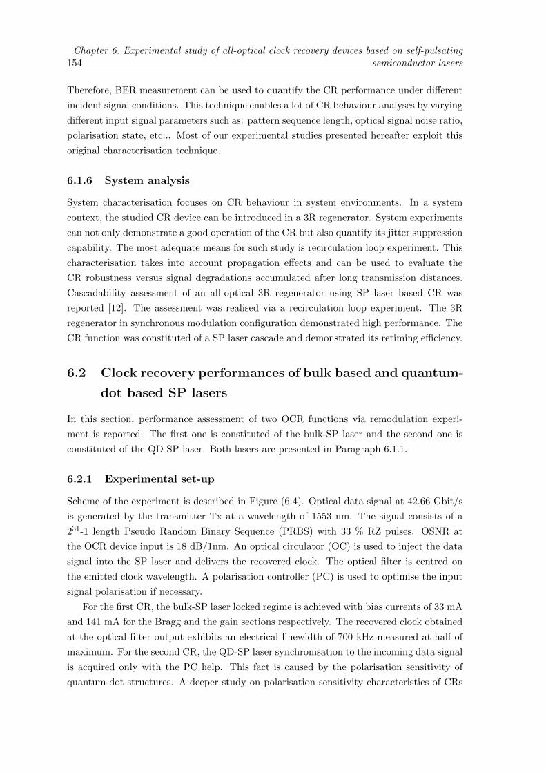
154Chapter 6. Experimental study of all-optical clock recovery devices based on self-pulsating
semiconductor lasers
Therefore, BER measurement can be used to quantify the CR performance under different
incident signal conditions. This technique enables a lot of CR behaviour analyses by varying
different input signal parameters such as: pattern sequence length, optical signal noise ratio,
polarisation state, etc... Most of our experimental studies presented hereafter exploit this
original characterisation technique.
6.1.6 System analysis
System characterisation focuses on CR behaviour in system environments. In a system
context, the studied CR device can be introduced in a 3R regenerator. System experiments
can not only demonstrate a good operation of the CR but also quantify its jitter suppression
capability. The most adequate means for such study is recirculation loop experiment. This
characterisation takes into account propagation effects and can be used to evaluate the
CR robustness versus signal degradations accumulated after long transmission distances.
Cascadability assessment of an all-optical 3R regenerator using SP laser based CR was
reported [12]. The assessment was realised via a recirculation loop experiment. The 3R
regenerator in synchronous modulation configuration demonstrated high performance. The
CR function was constituted of a SP laser cascade and demonstrated its retiming efficiency.
6.2 Clock recovery performances of bulk based and quantum-
dot based SP lasers
In this section, performance assessment of two OCR functions via remodulation experi-
ment is reported. The first one is constituted of the bulk-SP laser and the second one is
constituted of the QD-SP laser. Both lasers are presented in Paragraph 6.1.1.
6.2.1 Experimental set-up
Scheme of the experiment is described in Figure (6.4). Optical data signal at 42.66 Gbit/s
is generated by the transmitter Tx at a wavelength of 1553 nm. The signal consists of a
231-1 length Pseudo Random Binary Sequence (PRBS) with 33 % RZ pulses. OSNR at
the OCR device input is 18 dB/1nm. An optical circulator (OC) is used to inject the data
signal into the SP laser and delivers the recovered clock. The optical filter is centred on
the emitted clock wavelength. A polarisation controller (PC) is used to optimise the input
signal polarisation if necessary.
For the first CR, the bulk-SP laser locked regime is achieved with bias currents of 33 mA
and 141 mA for the Bragg and the gain sections respectively. The recovered clock obtained
at the optical filter output exhibits an electrical linewidth of 700 kHz measured at half of
maximum. For the second CR, the QD-SP laser synchronisation to the incoming data signal
is acquired only with the PC help. This fact is caused by the polarisation sensitivity of
quantum-dot structures. A deeper study on polarisation sensitivity characteristics of CRs
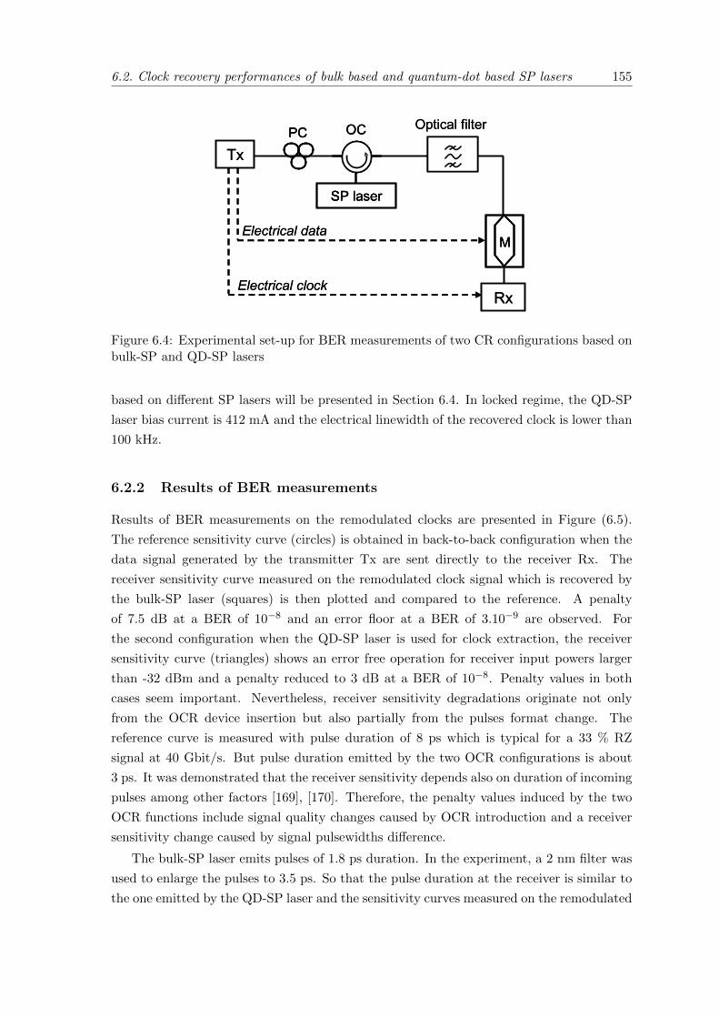
6.2. Clock recovery performances of bulk based and quantum-dot based SP lasers 155
Tx
Rx
PC
Electrical data
Electrical clock
M
Optical filter
SP laser
OC
Tx
Rx
PCPC
Electrical data
Electrical clock
MM
Optical filter
SP laser
OC
SP laser
OC
Figure 6.4: Experimental set-up for BER measurements of two CR configurations based onbulk-SP and QD-SP lasers
based on different SP lasers will be presented in Section 6.4. In locked regime, the QD-SP
laser bias current is 412 mA and the electrical linewidth of the recovered clock is lower than
100 kHz.
6.2.2 Results of BER measurements
Results of BER measurements on the remodulated clocks are presented in Figure (6.5).
The reference sensitivity curve (circles) is obtained in back-to-back configuration when the
data signal generated by the transmitter Tx are sent directly to the receiver Rx. The
receiver sensitivity curve measured on the remodulated clock signal which is recovered by
the bulk-SP laser (squares) is then plotted and compared to the reference. A penalty
of 7.5 dB at a BER of 10−8 and an error floor at a BER of 3.10−9 are observed. For
the second configuration when the QD-SP laser is used for clock extraction, the receiver
sensitivity curve (triangles) shows an error free operation for receiver input powers larger
than -32 dBm and a penalty reduced to 3 dB at a BER of 10−8. Penalty values in both
cases seem important. Nevertheless, receiver sensitivity degradations originate not only
from the OCR device insertion but also partially from the pulses format change. The
reference curve is measured with pulse duration of 8 ps which is typical for a 33 % RZ
signal at 40 Gbit/s. But pulse duration emitted by the two OCR configurations is about
3 ps. It was demonstrated that the receiver sensitivity depends also on duration of incoming
pulses among other factors [169], [170]. Therefore, the penalty values induced by the two
OCR functions include signal quality changes caused by OCR introduction and a receiver
sensitivity change caused by signal pulsewidths difference.
The bulk-SP laser emits pulses of 1.8 ps duration. In the experiment, a 2 nm filter was
used to enlarge the pulses to 3.5 ps. So that the pulse duration at the receiver is similar to
the one emitted by the QD-SP laser and the sensitivity curves measured on the remodulated
156Chapter 6. Experimental study of all-optical clock recovery devices based on self-pulsating
semiconductor lasers
1,E-101,E-091,E-081,E-071,E-061,E-051,E-041,E-031,E-021,E-01
-45 -40 -35 -30 -25 -20 -15 -10Input power Rx (dBm)
BER
ReferenceBulk-SP laserQD-SP laser
Figure 6.5: BER of a function of Rx input power for 2 OCRs based on bulk-SP laser andQD-SP laser
signals can be compared.
The BER results show clearly that the quality of the remodulated signal is better when
the QD-SP laser is used for the CR. A 4.5 dB penalty reduction at BER of 10−8 is achieved
and the error floor disappears. The signal degradations shown by the BER curves are
attributed to the poor clock quality recovered by the bulk-SP laser. This is probably due to
an excessive internal amplitude and phase noise in bulk structures and an insufficient jitter
filtering capability of the laser. On the other hand, the error free operation demonstrates
high clock quality and confirms good performance of the OCR based on QD-SP laser.
The performance difference between the OCRs based on bulk-SP laser and on QD-SP
laser brought out by the remodulation experiment is consistent with results reported by
other characterisations. It is shown that a QD-SP laser exhibits a better jitter suppression
capability in comparison to a bulk-SP laser [168]. In the same study, it is also demonstrated
that a narrower free running spectral linewidth corresponds to a transfer function with
smaller cut off frequency. In our case, the clock spectral linewidth of the bulk-SP laser is
1000 kHz compared to only 100 kHz of the QD-SP laser. This implies that the QD-SP laser
presents a higher jitter filtering efficiency. This advantage is achieved thanks to the high
spectral purity of quantum-dot based material and considered as the main explanation for
the BER measurement results.
To conclude, the bulk-SP laser shows insufficient timing jitter filtering effect. It is
difficult to use the laser to fulfil retiming task without any additional device to improve
the recovered clock quality. A simple and promising solution to enhance the bulk-SP laser
based CR performance is discussed in Section 6.3. Otherwise, the QD-SP laser emits a good
quality clock. This is demonstrated by an error free operation and a reduced penalty on the
receiver sensitivity curve of the remodulated clock signal. However, it is essential to note
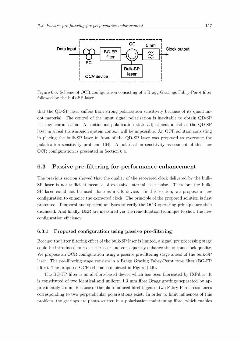
6.3. Passive pre-filtering for performance enhancement 157
OCR device
BG-FP filter
5 nm
Bulk-SP laser
OC
PC
Data input Clock output
OCR device
BG-FP filter
5 nm
Bulk-SP laser
OC
PC
OCR device
BG-FP filter
5 nm
Bulk-SP laser
Bulk-SP laser
OC
PCPC
Data input Clock output
Figure 6.6: Scheme of OCR configuration consisting of a Bragg Gratings Fabry-Perot filterfollowed by the bulk-SP laser
that the QD-SP laser suffers from strong polarisation sensitivity because of its quantum-
dot material. The control of the input signal polarisation is inevitable to obtain QD-SP
laser synchronisation. A continuous polarisation state adjustment ahead of the QD-SP
laser in a real transmission system context will be impossible. An OCR solution consisting
in placing the bulk-SP laser in front of the QD-SP laser was proposed to overcome the
polarisation sensitivity problem [164]. A polarisation sensitivity assessment of this new
OCR configuration is presented in Section 6.4.
6.3 Passive pre-filtering for performance enhancement
The previous section showed that the quality of the recovered clock delivered by the bulk-
SP laser is not sufficient because of excessive internal laser noise. Therefore the bulk-
SP laser could not be used alone as a CR device. In this section, we propose a new
configuration to enhance the extracted clock. The principle of the proposed solution is first
presented. Temporal and spectral analyses to verify the OCR operating principle are then
discussed. And finally, BER are measured via the remodulation technique to show the new
configuration efficiency.
6.3.1 Proposed configuration using passive pre-filtering
Because the jitter filtering effect of the bulk-SP laser is limited, a signal pre processing stage
could be introduced to assist the laser and consequently enhance the output clock quality.
We propose an OCR configuration using a passive pre-filtering stage ahead of the bulk-SP
laser. The pre-filtering stage consists in a Bragg Grating Fabry-Perot type filter (BG-FP
filter). The proposed OCR scheme is depicted in Figure (6.6).
The BG-FP filter is an all-fibre-based device which has been fabricated by IXFiber. It
is constituted of two identical and uniform 1.3 mm fibre Bragg gratings separated by ap-
proximately 2 mm. Because of the photoinduced birefringence, two Fabry-Perot resonances
corresponding to two perpendicular polarisations exist. In order to limit influences of this
problem, the gratings are photo-written in a polarisation maintaining fibre, which enables
158Chapter 6. Experimental study of all-optical clock recovery devices based on self-pulsating
semiconductor lasers
us to select separately one of the two resonances by adjusting the input polarisation. A
Polarisation Controller (PC) is therefore introduced to align the input signal polarisation
on one of the two intrinsic axes of the BG-FP filter fibre. The component is packaged in a
passive thermal insensitive module without temperature control. Data signal is injected to
the BG-FP filter via the PC. The intermediate clock obtained at the BG-FP filter output
is delivered to the bulk-SP laser via an optical circulator. A 5 nm optical band pass filter
is placed at the OC output which is centred on the wavelength of the final emitted clock.
Passive technique for OCR based on spectral line filtering has been largely investigated
[130], [171], [132]. Clock extraction could be obtained simply by injecting the data signal
into a periodic optical filter. However, high performance clock signals can be achieved only
with a very high finesse filter. In our case, the Fabry-Perot filter exhibits moderate finesse
but allows extracting an intermediate clock from the incoming data signal. The basic idea
is to use the filter in order to deliver a clock signal to the bulk-SP laser instead of the data
signal. Hence the laser can be synchronised regardless of pattern effects. The overall CR
task is shared between the pre-filtering stage and the SP laser. Thus efficiency requirements
on each component can be relaxed compared to the cases when each component is used
separately. At the OCR output we can expect a clock signal exhibiting a higher quality
than when the bulk-SP laser is used without pre-filtering.
6.3.2 Filter characterisation
The spectral transfer function of the BG-FP filter is measured by injecting an optical white
source and measuring the output optical spectrum. The measure is performed by using
a high precision optical spectrum analyser called BOSA (from Aragon Photonics) which
presents a spectral resolution of 0.08 pm. The transmission spectrum of the BG-FP filter
is shown in Figure (6.7).
The transmission peaks of the BG-FP filter correspond to two cavity Free Spectral Range
(FSR) sets because of the photoinduced birefringence mentioned previously. Separations
between main peaks of the two peak classes are 347 pm and 342 pm which corresponds
to FSR values of 43.2 GHz and 42.5 GHz respectively. The measured bandwidth at half
maximum is 0.7 pm for the central peak and 1.5 pm for the adjacent peaks. Thus, the finesse
of the central peak is very close to 500. It is important to note that with this bandwidth
range, the filter is not sensitive to the frequency jitter of the transmitter laser which is
typically less than 10 MHz (0.08 pm) for conventional DFB laser (used at the transmitter
Tx). The filter insertion loss is 7 dB.
The data signal at 42.7 Gbit/s is injected into the BG-FP filter via the PC. The optical
signal generated by the transmitter Tx is at 1553 nm. Signal polarisation at the filter
input is adjusted by using the PC and is aligned on one PM fibre intrinsic axis. The signal
is transmitted by the peak class exhibiting 42.5 GHz of FSR. Figure (6.8) displays the
temporal trace and the spectral trace of the intermediate clock signal at the BG-FP filter
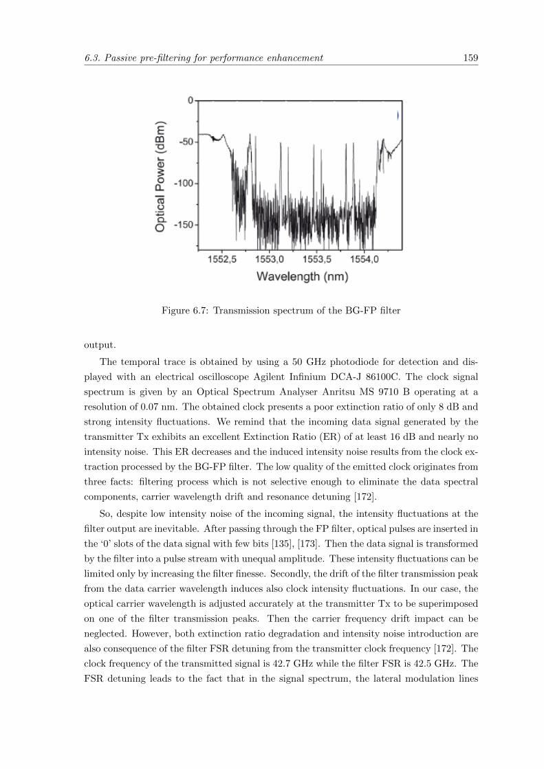
6.3. Passive pre-filtering for performance enhancement 159
Figure 6.7: Transmission spectrum of the BG-FP filter
output.
The temporal trace is obtained by using a 50 GHz photodiode for detection and dis-
played with an electrical oscilloscope Agilent Infinium DCA-J 86100C. The clock signal
spectrum is given by an Optical Spectrum Analyser Anritsu MS 9710 B operating at a
resolution of 0.07 nm. The obtained clock presents a poor extinction ratio of only 8 dB and
strong intensity fluctuations. We remind that the incoming data signal generated by the
transmitter Tx exhibits an excellent Extinction Ratio (ER) of at least 16 dB and nearly no
intensity noise. This ER decreases and the induced intensity noise results from the clock ex-
traction processed by the BG-FP filter. The low quality of the emitted clock originates from
three facts: filtering process which is not selective enough to eliminate the data spectral
components, carrier wavelength drift and resonance detuning [172].
So, despite low intensity noise of the incoming signal, the intensity fluctuations at the
filter output are inevitable. After passing through the FP filter, optical pulses are inserted in
the ‘0’ slots of the data signal with few bits [135], [173]. Then the data signal is transformed
by the filter into a pulse stream with unequal amplitude. These intensity fluctuations can be
limited only by increasing the filter finesse. Secondly, the drift of the filter transmission peak
from the data carrier wavelength induces also clock intensity fluctuations. In our case, the
optical carrier wavelength is adjusted accurately at the transmitter Tx to be superimposed
on one of the filter transmission peaks. Then the carrier frequency drift impact can be
neglected. However, both extinction ratio degradation and intensity noise introduction are
also consequence of the filter FSR detuning from the transmitter clock frequency [172]. The
clock frequency of the transmitted signal is 42.7 GHz while the filter FSR is 42.5 GHz. The
FSR detuning leads to the fact that in the signal spectrum, the lateral modulation lines
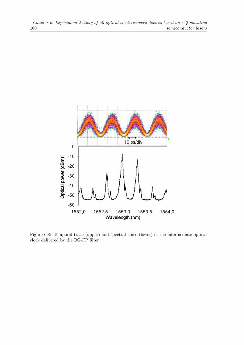
160Chapter 6. Experimental study of all-optical clock recovery devices based on self-pulsating
semiconductor lasers
-60
-50
-40
-30
-20
-10
0
1552,0 1552,5 1553,0 1553,5 1554,0Wavelength (nm)
Opt
ical
pow
er (d
Bm
)
10 ps/div
-60
-50
-40
-30
-20
-10
0
1552,0 1552,5 1553,0 1553,5 1554,0Wavelength (nm)
Opt
ical
pow
er (d
Bm
)
-60
-50
-40
-30
-20
-10
0
1552,0 1552,5 1553,0 1553,5 1554,0Wavelength (nm)
Opt
ical
pow
er (d
Bm
)
10 ps/div10 ps/div
Figure 6.8: Temporal trace (upper) and spectral trace (lower) of the intermediate opticalclock delivered by the BG-FP filter
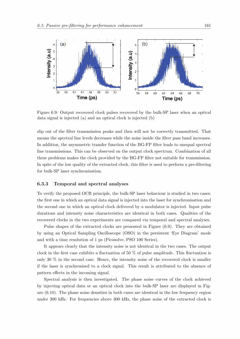
6.3. Passive pre-filtering for performance enhancement 161
Time (ps)
Inte
nsity
(a.u
)
Time (ps)
Inte
nsity
(a.u
)
Time (ps)
Inte
nsity
(a.u
)
Time (ps)
Inte
nsity
(a.u
)
Time (ps)
Inte
nsity
(a.u
)
Time (ps)
Inte
nsity
(a.u
)
Figure 6.9: Output recovered clock pulses recovered by the bulk-SP laser when an opticaldata signal is injected (a) and an optical clock is injected (b)
slip out of the filter transmission peaks and then will not be correctly transmitted. That
means the spectral line levels decreases while the noise inside the filter pass band increases.
In addition, the asymmetric transfer function of the BG-FP filter leads to unequal spectral
line transmissions. This can be observed on the output clock spectrum. Combination of all
these problems makes the clock provided by the BG-FP filter not suitable for transmission.
In spite of the low quality of the extracted clock, this filter is used to perform a pre-filtering
for bulk-SP laser synchronisation.
6.3.3 Temporal and spectral analyses
To verify the proposed OCR principle, the bulk-SP laser behaviour is studied in two cases:
the first one in which an optical data signal is injected into the laser for synchronisation and
the second one in which an optical clock delivered by a modulator is injected. Input pulse
durations and intensity noise characteristics are identical in both cases. Qualities of the
recovered clocks in the two experiments are compared via temporal and spectral analyses.
Pulse shapes of the extracted clocks are presented in Figure (6.9). They are obtained
by using an Optical Sampling Oscilloscope (OSO) in the persistent ‘Eye Diagram’ mode
and with a time resolution of 1 ps (Picosolve, PSO 100 Series).
It appears clearly that the intensity noise is not identical in the two cases. The output
clock in the first case exhibits a fluctuation of 50 % of pulse amplitude. This fluctuation is
only 30 % in the second case. Hence, the intensity noise of the recovered clock is smaller
if the laser is synchronised to a clock signal. This result is attributed to the absence of
pattern effects in the incoming signal.
Spectral analysis is then investigated. The phase noise curves of the clock achieved
by injecting optical data or an optical clock into the bulk-SP laser are displayed in Fig-
ure (6.10). The phase noise densities in both cases are identical in the low frequency region
under 300 kHz. For frequencies above 300 kHz, the phase noise of the extracted clock is
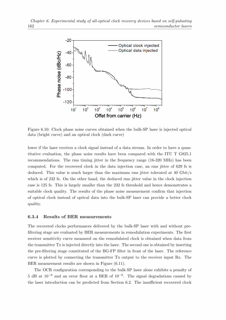
162Chapter 6. Experimental study of all-optical clock recovery devices based on self-pulsating
semiconductor lasers
Offet from carrier (Hz)
Phas
e no
ise
(dBc
/Hz)
Offet from carrier (Hz)
Phas
e no
ise
(dBc
/Hz)
Figure 6.10: Clock phase noise curves obtained when the bulk-SP laser is injected opticaldata (bright curve) and an optical clock (dark curve)
lower if the laser receives a clock signal instead of a data stream. In order to have a quan-
titative evaluation, the phase noise results have been compared with the ITU T G825.1
recommendations. The rms timing jitter in the frequency range (16-320 MHz) has been
computed. For the recovered clock in the data injection case, an rms jitter of 629 fs is
deduced. This value is much larger than the maximum rms jitter tolerated at 40 Gbit/s
which is of 232 fs. On the other hand, the deduced rms jitter value in the clock injection
case is 125 fs. This is largely smaller than the 232 fs threshold and hence demonstrates a
suitable clock quality. The results of the phase noise measurement confirm that injection
of optical clock instead of optical data into the bulk-SP laser can provide a better clock
quality.
6.3.4 Results of BER measurements
The recovered clocks performances delivered by the bulk-SP laser with and without pre-
filtering stage are evaluated by BER measurements in remodulation experiments. The first
receiver sensitivity curve measured on the remodulated clock is obtained when data from
the transmitter Tx is injected directly into the laser. The second one is obtained by inserting
the pre-filtering stage constituted of the BG-FP filter in front of the laser. The reference
curve is plotted by connecting the transmitter Tx output to the receiver input Rx. The
BER measurement results are shown in Figure (6.11).
The OCR configuration corresponding to the bulk-SP laser alone exhibits a penalty of
5 dB at 10−8 and an error floor at a BER of 10−9. The signal degradations caused by
the laser introduction can be predicted from Section 6.2. The insufficient recovered clock
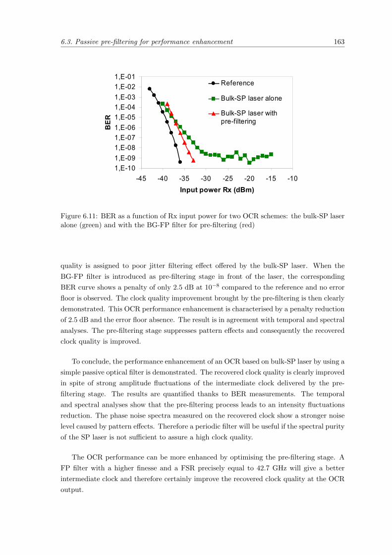
6.3. Passive pre-filtering for performance enhancement 163
1,E-101,E-091,E-081,E-071,E-061,E-051,E-041,E-031,E-021,E-01
-45 -40 -35 -30 -25 -20 -15 -10Input power Rx (dBm)
BER
Reference
Bulk-SP laser alone
Bulk-SP laser withpre-filtering
Figure 6.11: BER as a function of Rx input power for two OCR schemes: the bulk-SP laseralone (green) and with the BG-FP filter for pre-filtering (red)
quality is assigned to poor jitter filtering effect offered by the bulk-SP laser. When the
BG-FP filter is introduced as pre-filtering stage in front of the laser, the corresponding
BER curve shows a penalty of only 2.5 dB at 10−8 compared to the reference and no error
floor is observed. The clock quality improvement brought by the pre-filtering is then clearly
demonstrated. This OCR performance enhancement is characterised by a penalty reduction
of 2.5 dB and the error floor absence. The result is in agreement with temporal and spectral
analyses. The pre-filtering stage suppresses pattern effects and consequently the recovered
clock quality is improved.
To conclude, the performance enhancement of an OCR based on bulk-SP laser by using a
simple passive optical filter is demonstrated. The recovered clock quality is clearly improved
in spite of strong amplitude fluctuations of the intermediate clock delivered by the pre-
filtering stage. The results are quantified thanks to BER measurements. The temporal
and spectral analyses show that the pre-filtering process leads to an intensity fluctuations
reduction. The phase noise spectra measured on the recovered clock show a stronger noise
level caused by pattern effects. Therefore a periodic filter will be useful if the spectral purity
of the SP laser is not sufficient to assure a high clock quality.
The OCR performance can be more enhanced by optimising the pre-filtering stage. A
FP filter with a higher finesse and a FSR precisely equal to 42.7 GHz will give a better
intermediate clock and therefore certainly improve the recovered clock quality at the OCR
output.
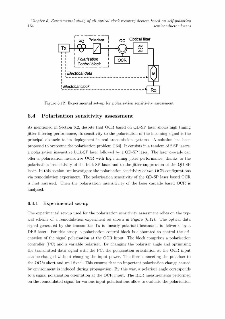
164Chapter 6. Experimental study of all-optical clock recovery devices based on self-pulsating
semiconductor lasers
Tx
Rx
PC
Electrical data
Electrical clock
M
Optical filter
OCR
OCPolariser
PolarisationControl block
Tx
Rx
PCPC
Electrical data
Electrical clock
MM
Optical filterOptical filter
OCR
OC
OCR
OCPolariserPolariser
PolarisationControl block
Figure 6.12: Experimental set-up for polarisation sensitivity assessment
6.4 Polarisation sensitivity assessment
As mentioned in Section 6.2, despite that OCR based on QD-SP laser shows high timing
jitter filtering performance, its sensitivity to the polarisation of the incoming signal is the
principal obstacle to its deployment in real transmission systems. A solution has been
proposed to overcome the polarisation problem [164]. It consists in a tandem of 2 SP lasers:
a polarisation insensitive bulk-SP laser followed by a QD-SP laser. The laser cascade can
offer a polarisation insensitive OCR with high timing jitter performance, thanks to the
polarisation insensitivity of the bulk-SP laser and to the jitter suppression of the QD-SP
laser. In this section, we investigate the polarisation sensitivity of two OCR configurations
via remodulation experiment. The polarisation sensitivity of the QD-SP laser based OCR
is first assessed. Then the polarisation insensitivity of the laser cascade based OCR is
analysed.
6.4.1 Experimental set-up
The experimental set-up used for the polarisation sensitivity assessment relies on the typ-
ical scheme of a remodulation experiment as shown in Figure (6.12). The optical data
signal generated by the transmitter Tx is linearly polarised because it is delivered by a
DFB laser. For this study, a polarisation control block is elaborated to control the ori-
entation of the signal polarisation at the OCR input. The block comprises a polarisation
controller (PC) and a variable polariser. By changing the polariser angle and optimising
the transmitted data signal with the PC, the polarisation orientation at the OCR input
can be changed without changing the input power. The fibre connecting the polariser to
the OC is short and well fixed. This ensures that no important polarisation change caused
by environment is induced during propagation. By this way, a polariser angle corresponds
to a signal polarisation orientation at the OCR input. The BER measurements performed
on the remodulated signal for various input polarisations allow to evaluate the polarisation
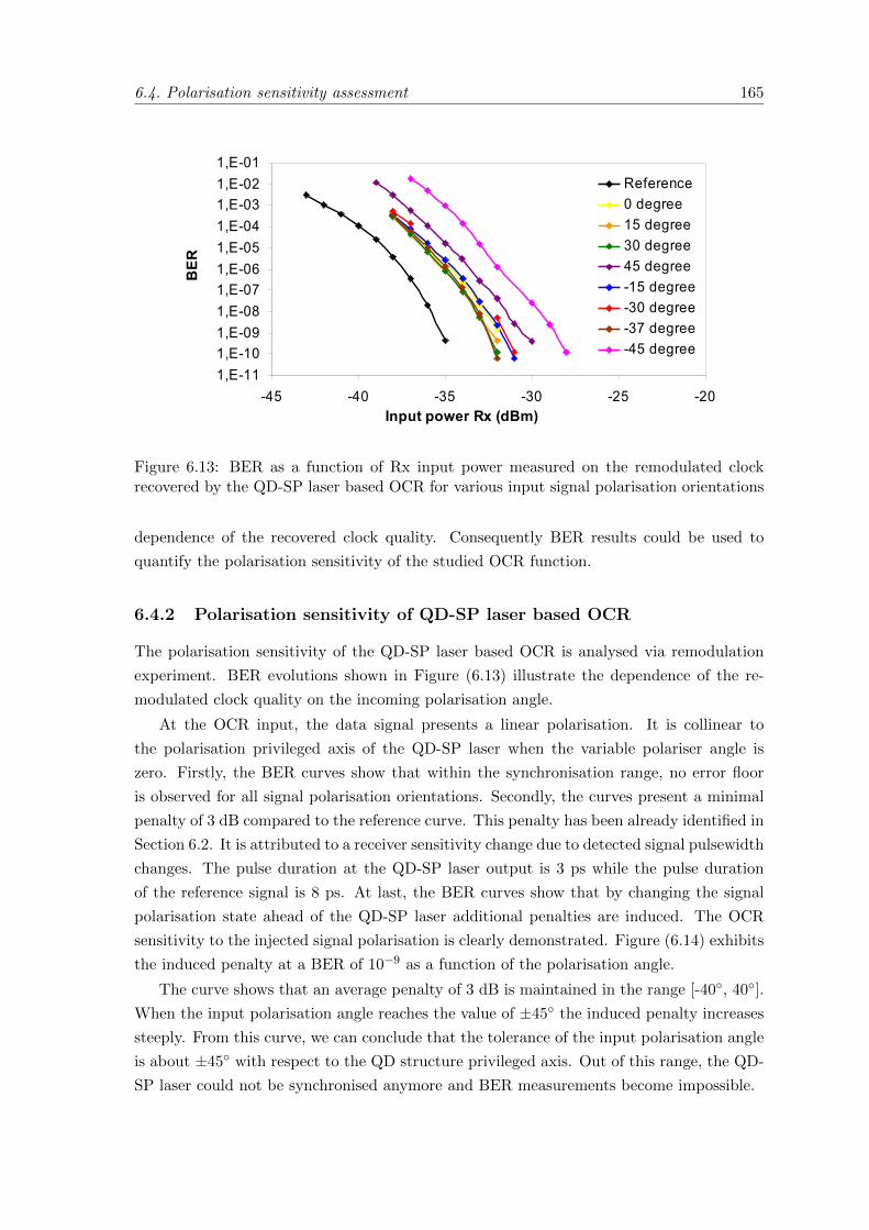
6.4. Polarisation sensitivity assessment 165
1,E-111,E-101,E-091,E-081,E-071,E-061,E-051,E-041,E-031,E-021,E-01
-45 -40 -35 -30 -25 -20Input power Rx (dBm)
BER
Reference0 degree15 degree30 degree45 degree-15 degree-30 degree-37 degree-45 degree
Figure 6.13: BER as a function of Rx input power measured on the remodulated clockrecovered by the QD-SP laser based OCR for various input signal polarisation orientations
dependence of the recovered clock quality. Consequently BER results could be used to
quantify the polarisation sensitivity of the studied OCR function.
6.4.2 Polarisation sensitivity of QD-SP laser based OCR
The polarisation sensitivity of the QD-SP laser based OCR is analysed via remodulation
experiment. BER evolutions shown in Figure (6.13) illustrate the dependence of the re-
modulated clock quality on the incoming polarisation angle.
At the OCR input, the data signal presents a linear polarisation. It is collinear to
the polarisation privileged axis of the QD-SP laser when the variable polariser angle is
zero. Firstly, the BER curves show that within the synchronisation range, no error floor
is observed for all signal polarisation orientations. Secondly, the curves present a minimal
penalty of 3 dB compared to the reference curve. This penalty has been already identified in
Section 6.2. It is attributed to a receiver sensitivity change due to detected signal pulsewidth
changes. The pulse duration at the QD-SP laser output is 3 ps while the pulse duration
of the reference signal is 8 ps. At last, the BER curves show that by changing the signal
polarisation state ahead of the QD-SP laser additional penalties are induced. The OCR
sensitivity to the injected signal polarisation is clearly demonstrated. Figure (6.14) exhibits
the induced penalty at a BER of 10−9 as a function of the polarisation angle.
The curve shows that an average penalty of 3 dB is maintained in the range [-40◦, 40◦].
When the input polarisation angle reaches the value of ±45◦ the induced penalty increases
steeply. From this curve, we can conclude that the tolerance of the input polarisation angle
is about ±45◦ with respect to the QD structure privileged axis. Out of this range, the QD-
SP laser could not be synchronised anymore and BER measurements become impossible.
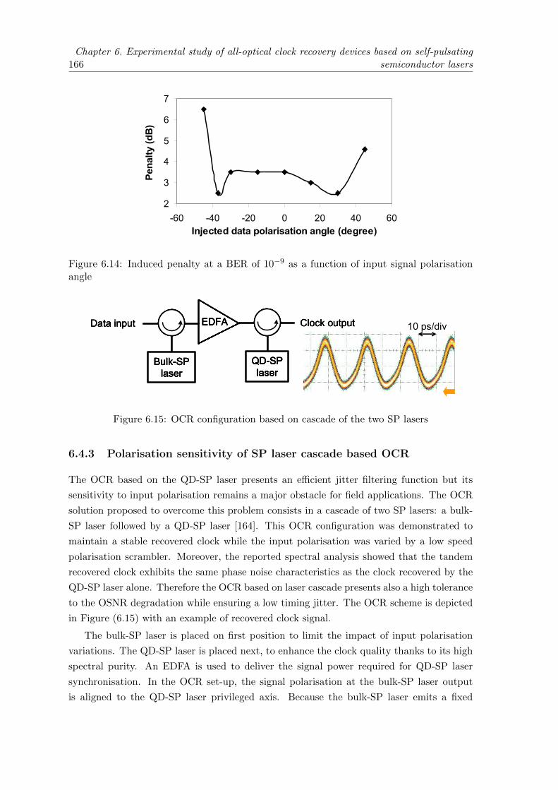
166Chapter 6. Experimental study of all-optical clock recovery devices based on self-pulsating
semiconductor lasers
2
3
4
5
6
7
-60 -40 -20 0 20 40 60Injected data polarisation angle (degree)
Pena
lty (d
B)
Figure 6.14: Induced penalty at a BER of 10−9 as a function of input signal polarisationangle
EDFA
Bulk-SPlaser
QD-SPlaser
Data input Clock output 10 ps/divEDFA
Bulk-SPlaser
QD-SPlaser
Data input Clock outputEDFA
Bulk-SPlaser
QD-SPlaser
EDFAEDFA
Bulk-SPlaser
Bulk-SPlaser
QD-SPlaser
QD-SPlaser
Data input Clock output 10 ps/div10 ps/div10 ps/div
Figure 6.15: OCR configuration based on cascade of the two SP lasers
6.4.3 Polarisation sensitivity of SP laser cascade based OCR
The OCR based on the QD-SP laser presents an efficient jitter filtering function but its
sensitivity to input polarisation remains a major obstacle for field applications. The OCR
solution proposed to overcome this problem consists in a cascade of two SP lasers: a bulk-
SP laser followed by a QD-SP laser [164]. This OCR configuration was demonstrated to
maintain a stable recovered clock while the input polarisation was varied by a low speed
polarisation scrambler. Moreover, the reported spectral analysis showed that the tandem
recovered clock exhibits the same phase noise characteristics as the clock recovered by the
QD-SP laser alone. Therefore the OCR based on laser cascade presents also a high tolerance
to the OSNR degradation while ensuring a low timing jitter. The OCR scheme is depicted
in Figure (6.15) with an example of recovered clock signal.
The bulk-SP laser is placed on first position to limit the impact of input polarisation
variations. The QD-SP laser is placed next, to enhance the clock quality thanks to its high
spectral purity. An EDFA is used to deliver the signal power required for QD-SP laser
synchronisation. In the OCR set-up, the signal polarisation at the bulk-SP laser output
is aligned to the QD-SP laser privileged axis. Because the bulk-SP laser emits a fixed
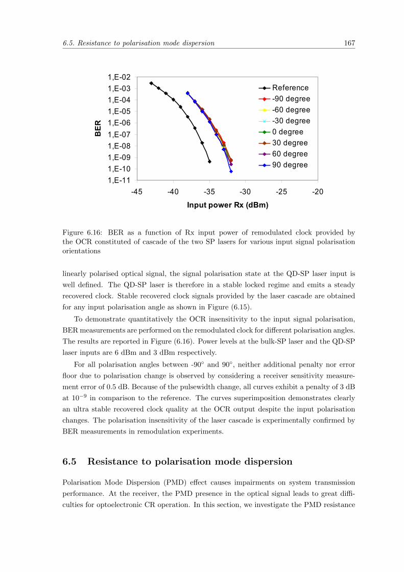
6.5. Resistance to polarisation mode dispersion 167
1,E-111,E-101,E-091,E-081,E-071,E-061,E-051,E-041,E-031,E-02
-45 -40 -35 -30 -25 -20
Input power Rx (dBm)
BER
Reference-90 degree-60 degree-30 degree0 degree30 degree60 degree90 degree
Figure 6.16: BER as a function of Rx input power of remodulated clock provided bythe OCR constituted of cascade of the two SP lasers for various input signal polarisationorientations
linearly polarised optical signal, the signal polarisation state at the QD-SP laser input is
well defined. The QD-SP laser is therefore in a stable locked regime and emits a steady
recovered clock. Stable recovered clock signals provided by the laser cascade are obtained
for any input polarisation angle as shown in Figure (6.15).
To demonstrate quantitatively the OCR insensitivity to the input signal polarisation,
BER measurements are performed on the remodulated clock for different polarisation angles.
The results are reported in Figure (6.16). Power levels at the bulk-SP laser and the QD-SP
laser inputs are 6 dBm and 3 dBm respectively.
For all polarisation angles between -90◦ and 90◦, neither additional penalty nor error
floor due to polarisation change is observed by considering a receiver sensitivity measure-
ment error of 0.5 dB. Because of the pulsewidth change, all curves exhibit a penalty of 3 dB
at 10−9 in comparison to the reference. The curves superimposition demonstrates clearly
an ultra stable recovered clock quality at the OCR output despite the input polarisation
changes. The polarisation insensitivity of the laser cascade is experimentally confirmed by
BER measurements in remodulation experiments.
6.5 Resistance to polarisation mode dispersion
Polarisation Mode Dispersion (PMD) effect causes impairments on system transmission
performance. At the receiver, the PMD presence in the optical signal leads to great diffi-
culties for optoelectronic CR operation. In this section, we investigate the PMD resistance
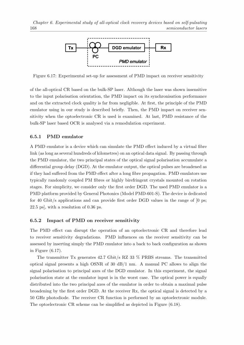
168Chapter 6. Experimental study of all-optical clock recovery devices based on self-pulsating
semiconductor lasers
Tx Rx
PC
DGD emulator
PMD emulator
Tx Rx
PC
DGD emulator
PMD emulatorPCPC
DGD emulator
PMD emulator
Figure 6.17: Experimental set-up for assessment of PMD impact on receiver sensitivity
of the all-optical CR based on the bulk-SP laser. Although the laser was shown insensitive
to the input polarisation orientation, the PMD impact on its synchronisation performance
and on the extracted clock quality is far from negligible. At first, the principle of the PMD
emulator using in our study is described briefly. Then, the PMD impact on receiver sen-
sitivity when the optoelectronic CR is used is examined. At last, PMD resistance of the
bulk-SP laser based OCR is analysed via a remodulation experiment.
6.5.1 PMD emulator
A PMD emulator is a device which can simulate the PMD effect induced by a virtual fibre
link (as long as several hundreds of kilometres) on an optical data signal. By passing through
the PMD emulator, the two principal states of the optical signal polarisation accumulate a
differential group delay (DGD). At the emulator output, the optical pulses are broadened as
if they had suffered from the PMD effect after a long fibre propagation. PMD emulators use
typically randomly coupled PM fibres or highly birefringent crystals mounted on rotation
stages. For simplicity, we consider only the first order DGD. The used PMD emulator is a
PMD platform provided by General Photonics (Model PMD-601-S). The device is dedicated
for 40 Gbit/s applications and can provide first order DGD values in the range of [0 ps;
22.5 ps], with a resolution of 0.36 ps.
6.5.2 Impact of PMD on receiver sensitivity
The PMD effect can disrupt the operation of an optoelectronic CR and therefore lead
to receiver sensitivity degradations. PMD influences on the receiver sensitivity can be
assessed by inserting simply the PMD emulator into a back to back configuration as shown
in Figure (6.17).
The transmitter Tx generates 42.7 Gbit/s RZ 33 % PRBS streams. The transmitted
optical signal presents a high OSNR of 30 dB/1 nm. A manual PC allows to align the
signal polarisation to principal axes of the DGD emulator. In this experiment, the signal
polarisation state at the emulator input is in the worst case. The optical power is equally
distributed into the two principal axes of the emulator in order to obtain a maximal pulse
broadening by the first order DGD. At the receiver Rx, the optical signal is detected by a
50 GHz photodiode. The receiver CR function is performed by an optoelectronic module.
The optoelectronic CR scheme can be simplified as depicted in Figure (6.18).
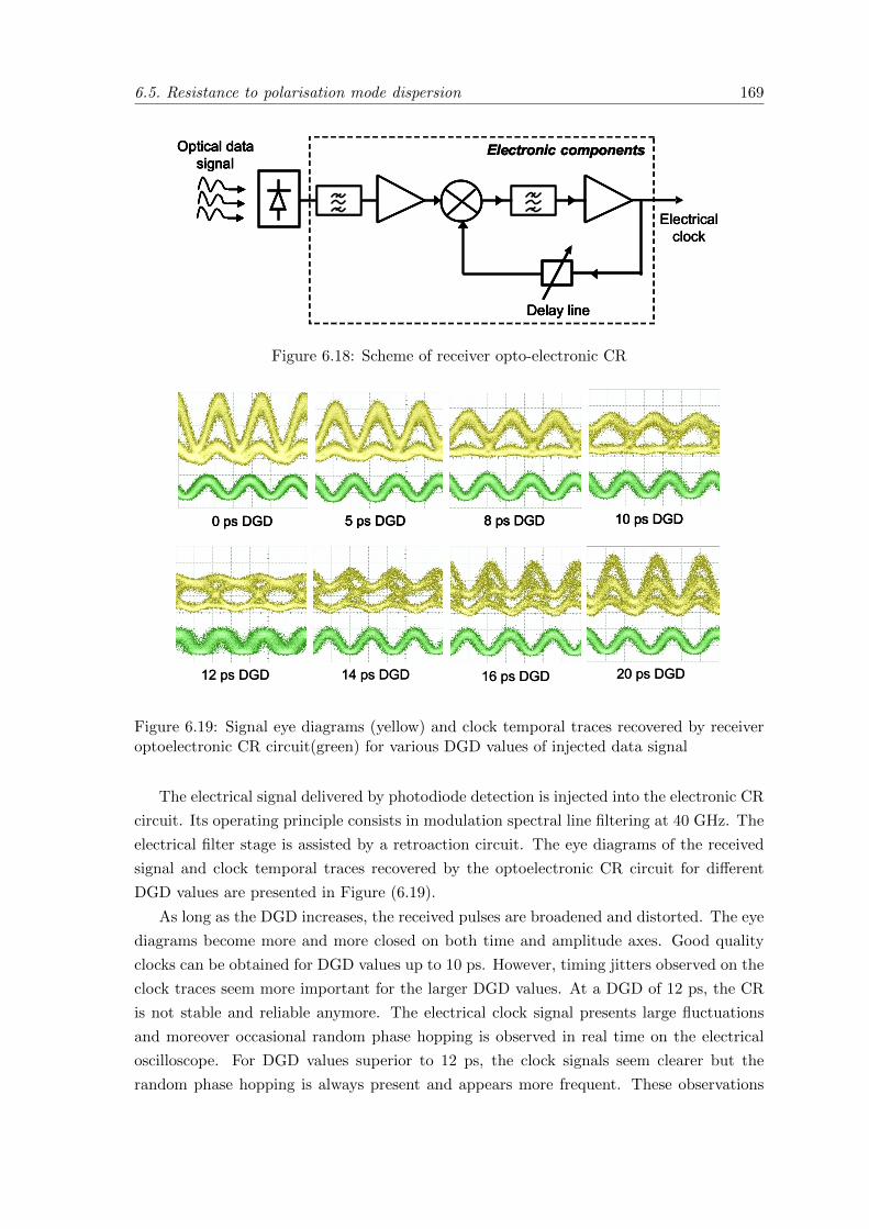
6.5. Resistance to polarisation mode dispersion 169
Optical data signal
Delay line
Electricalclock
Electronic componentsOptical data signal
Delay line
Electricalclock
Electronic componentsOptical data signal
Optical data signal
Delay lineDelay line
Electricalclock
Electronic components
Figure 6.18: Scheme of receiver opto-electronic CR
0 ps DGD 5 ps DGD 8 ps DGD 10 ps DGD
12 ps DGD 14 ps DGD 16 ps DGD 20 ps DGD
0 ps DGD 5 ps DGD 8 ps DGD 10 ps DGD0 ps DGD 5 ps DGD 8 ps DGD 10 ps DGD
12 ps DGD 14 ps DGD 16 ps DGD 20 ps DGD
Figure 6.19: Signal eye diagrams (yellow) and clock temporal traces recovered by receiveroptoelectronic CR circuit(green) for various DGD values of injected data signal
The electrical signal delivered by photodiode detection is injected into the electronic CR
circuit. Its operating principle consists in modulation spectral line filtering at 40 GHz. The
electrical filter stage is assisted by a retroaction circuit. The eye diagrams of the received
signal and clock temporal traces recovered by the optoelectronic CR circuit for different
DGD values are presented in Figure (6.19).
As long as the DGD increases, the received pulses are broadened and distorted. The eye
diagrams become more and more closed on both time and amplitude axes. Good quality
clocks can be obtained for DGD values up to 10 ps. However, timing jitters observed on the
clock traces seem more important for the larger DGD values. At a DGD of 12 ps, the CR
is not stable and reliable anymore. The electrical clock signal presents large fluctuations
and moreover occasional random phase hopping is observed in real time on the electrical
oscilloscope. For DGD values superior to 12 ps, the clock signals seem clearer but the
random phase hopping is always present and appears more frequent. These observations
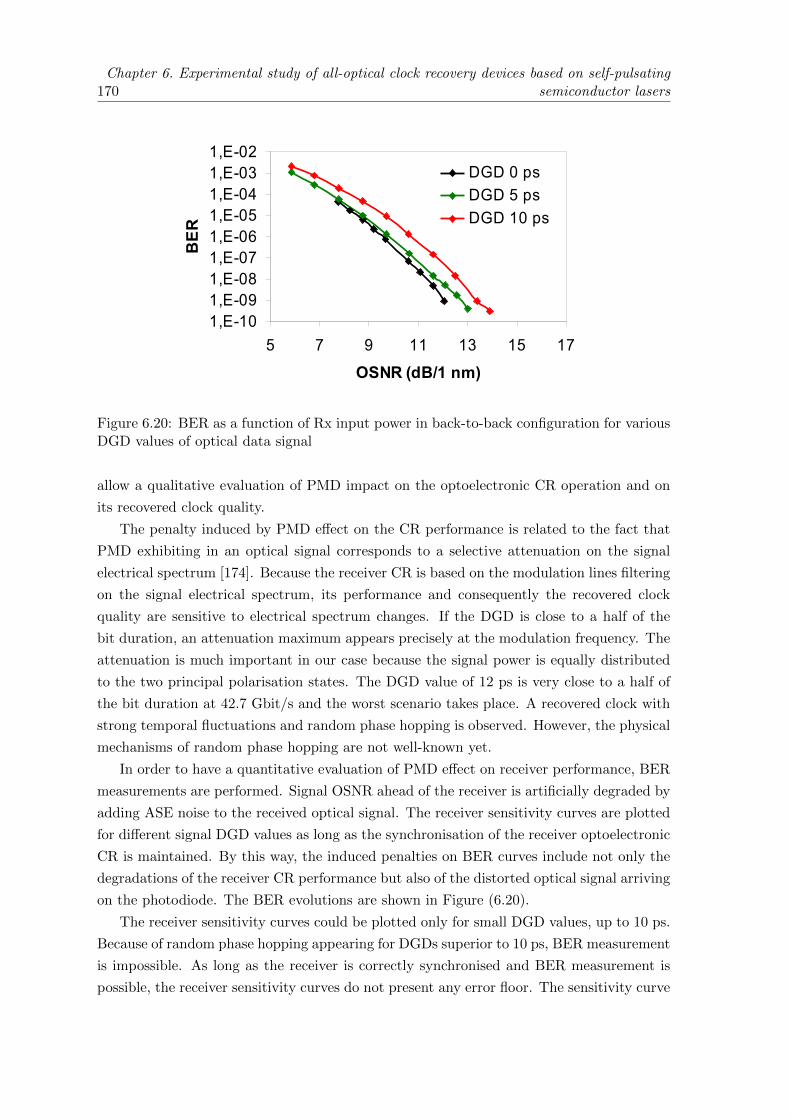
170Chapter 6. Experimental study of all-optical clock recovery devices based on self-pulsating
semiconductor lasers
1,E-101,E-091,E-081,E-071,E-061,E-051,E-041,E-031,E-02
5 7 9 11 13 15 17
OSNR (dB/1 nm)
BER
DGD 0 psDGD 5 psDGD 10 ps
Figure 6.20: BER as a function of Rx input power in back-to-back configuration for variousDGD values of optical data signal
allow a qualitative evaluation of PMD impact on the optoelectronic CR operation and on
its recovered clock quality.
The penalty induced by PMD effect on the CR performance is related to the fact that
PMD exhibiting in an optical signal corresponds to a selective attenuation on the signal
electrical spectrum [174]. Because the receiver CR is based on the modulation lines filtering
on the signal electrical spectrum, its performance and consequently the recovered clock
quality are sensitive to electrical spectrum changes. If the DGD is close to a half of the
bit duration, an attenuation maximum appears precisely at the modulation frequency. The
attenuation is much important in our case because the signal power is equally distributed
to the two principal polarisation states. The DGD value of 12 ps is very close to a half of
the bit duration at 42.7 Gbit/s and the worst scenario takes place. A recovered clock with
strong temporal fluctuations and random phase hopping is observed. However, the physical
mechanisms of random phase hopping are not well-known yet.
In order to have a quantitative evaluation of PMD effect on receiver performance, BER
measurements are performed. Signal OSNR ahead of the receiver is artificially degraded by
adding ASE noise to the received optical signal. The receiver sensitivity curves are plotted
for different signal DGD values as long as the synchronisation of the receiver optoelectronic
CR is maintained. By this way, the induced penalties on BER curves include not only the
degradations of the receiver CR performance but also of the distorted optical signal arriving
on the photodiode. The BER evolutions are shown in Figure (6.20).
The receiver sensitivity curves could be plotted only for small DGD values, up to 10 ps.
Because of random phase hopping appearing for DGDs superior to 10 ps, BER measurement
is impossible. As long as the receiver is correctly synchronised and BER measurement is
possible, the receiver sensitivity curves do not present any error floor. The sensitivity curve
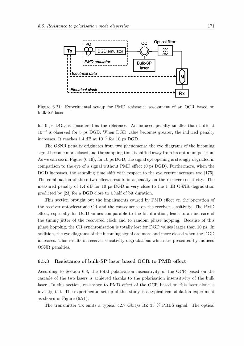
6.5. Resistance to polarisation mode dispersion 171
TxPC
Electrical data
Electrical clockRx
M
Optical filter
Bulk-SP laser
OC
DGD emulator
PMD emulator
TxPCPC
Electrical data
Electrical clockRx
M
Rx
MM
Optical filterOptical filter
Bulk-SP laser
OC
DGD emulator
PMD emulator
DGD emulator
PMD emulator
Figure 6.21: Experimental set-up for PMD resistance assessment of an OCR based onbulk-SP laser
for 0 ps DGD is considered as the reference. An induced penalty smaller than 1 dB at
10−9 is observed for 5 ps DGD. When DGD value becomes greater, the induced penalty
increases. It reaches 1.4 dB at 10−9 for 10 ps DGD.
The OSNR penalty originates from two phenomena: the eye diagrams of the incoming
signal become more closed and the sampling time is shifted away from its optimum position.
As we can see in Figure (6.19), for 10 ps DGD, the signal eye opening is strongly degraded in
comparison to the eye of a signal without PMD effect (0 ps DGD). Furthermore, when the
DGD increases, the sampling time shift with respect to the eye centre increases too [175].
The combination of these two effects results in a penalty on the receiver sensitivity. The
measured penalty of 1.4 dB for 10 ps DGD is very close to the 1 dB OSNR degradation
predicted by [23] for a DGD close to a half of bit duration.
This section brought out the impairments caused by PMD effect on the operation of
the receiver optoelectronic CR and the consequence on the receiver sensitivity. The PMD
effect, especially for DGD values comparable to the bit duration, leads to an increase of
the timing jitter of the recovered clock and to random phase hopping. Because of this
phase hopping, the CR synchronisation is totally lost for DGD values larger than 10 ps. In
addition, the eye diagrams of the incoming signal are more and more closed when the DGD
increases. This results in receiver sensitivity degradations which are presented by induced
OSNR penalties.
6.5.3 Resistance of bulk-SP laser based OCR to PMD effect
According to Section 6.3, the total polarisation insensitivity of the OCR based on the
cascade of the two lasers is achieved thanks to the polarisation insensitivity of the bulk
laser. In this section, resistance to PMD effect of the OCR based on this laser alone is
investigated. The experimental set-up of this study is a typical remodulation experiment
as shown in Figure (6.21).
The transmitter Tx emits a typical 42.7 Gbit/s RZ 33 % PRBS signal. The optical
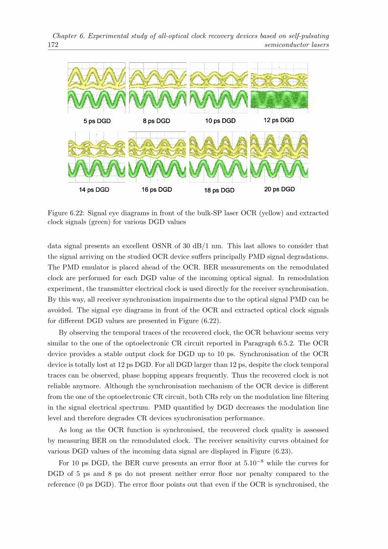
172Chapter 6. Experimental study of all-optical clock recovery devices based on self-pulsating
semiconductor lasers
5 ps DGD 8 ps DGD 10 ps DGD 12 ps DGD
14 ps DGD 16 ps DGD 18 ps DGD 20 ps DGD
5 ps DGD 8 ps DGD 10 ps DGD 12 ps DGD
14 ps DGD 16 ps DGD 18 ps DGD 20 ps DGD
Figure 6.22: Signal eye diagrams in front of the bulk-SP laser OCR (yellow) and extractedclock signals (green) for various DGD values
data signal presents an excellent OSNR of 30 dB/1 nm. This last allows to consider that
the signal arriving on the studied OCR device suffers principally PMD signal degradations.
The PMD emulator is placed ahead of the OCR. BER measurements on the remodulated
clock are performed for each DGD value of the incoming optical signal. In remodulation
experiment, the transmitter electrical clock is used directly for the receiver synchronisation.
By this way, all receiver synchronisation impairments due to the optical signal PMD can be
avoided. The signal eye diagrams in front of the OCR and extracted optical clock signals
for different DGD values are presented in Figure (6.22).
By observing the temporal traces of the recovered clock, the OCR behaviour seems very
similar to the one of the optoelectronic CR circuit reported in Paragraph 6.5.2. The OCR
device provides a stable output clock for DGD up to 10 ps. Synchronisation of the OCR
device is totally lost at 12 ps DGD. For all DGD larger than 12 ps, despite the clock temporal
traces can be observed, phase hopping appears frequently. Thus the recovered clock is not
reliable anymore. Although the synchronisation mechanism of the OCR device is different
from the one of the optoelectronic CR circuit, both CRs rely on the modulation line filtering
in the signal electrical spectrum. PMD quantified by DGD decreases the modulation line
level and therefore degrades CR devices synchronisation performance.
As long as the OCR function is synchronised, the recovered clock quality is assessed
by measuring BER on the remodulated clock. The receiver sensitivity curves obtained for
various DGD values of the incoming data signal are displayed in Figure (6.23).
For 10 ps DGD, the BER curve presents an error floor at 5.10−8 while the curves for
DGD of 5 ps and 8 ps do not present neither error floor nor penalty compared to the
reference (0 ps DGD). The error floor points out that even if the OCR is synchronised, the
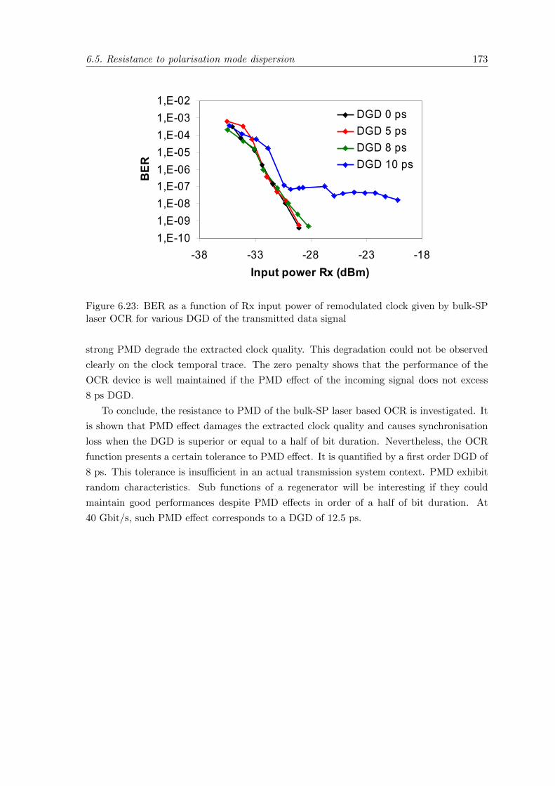
6.5. Resistance to polarisation mode dispersion 173
1,E-101,E-091,E-081,E-071,E-061,E-051,E-041,E-031,E-02
-38 -33 -28 -23 -18Input power Rx (dBm)
BER
DGD 0 psDGD 5 psDGD 8 psDGD 10 ps
Figure 6.23: BER as a function of Rx input power of remodulated clock given by bulk-SPlaser OCR for various DGD of the transmitted data signal
strong PMD degrade the extracted clock quality. This degradation could not be observed
clearly on the clock temporal trace. The zero penalty shows that the performance of the
OCR device is well maintained if the PMD effect of the incoming signal does not excess
8 ps DGD.
To conclude, the resistance to PMD of the bulk-SP laser based OCR is investigated. It
is shown that PMD effect damages the extracted clock quality and causes synchronisation
loss when the DGD is superior or equal to a half of bit duration. Nevertheless, the OCR
function presents a certain tolerance to PMD effect. It is quantified by a first order DGD of
8 ps. This tolerance is insufficient in an actual transmission system context. PMD exhibit
random characteristics. Sub functions of a regenerator will be interesting if they could
maintain good performances despite PMD effects in order of a half of bit duration. At
40 Gbit/s, such PMD effect corresponds to a DGD of 12.5 ps.

174 Summary of optical clock recovery investigations
Summary of optical clock recovery
investigations
This second part of the manuscript is devoted to present the experimental assessments of
different all-optical clock recovery configurations. The studied OCR functions are princi-
pally based on self-pulsating semiconductor lasers.
In the fifth chapter, roles of CR function in optical networks are firstly discussed. It
is pointed out that regardless of the CR function position, at receivers, in node of OTDM
systems or in in-line repeaters, the recovered clocks must have a low timing jitter. The clock
quality defines the timing stability and synchronisation performance of the overall commu-
nication system. Then, different techniques which are usually exploited for CR devices
are briefly reviewed. They are classified in three categories according to their operation
principles: spectral filtering technique, phase-locked loop technique and injection locking
in oscillating systems. The principle, virtues as well as drawbacks of each technique are
discussed. It is shown that to go beyond 40 Gbit/s, the CR devices which are constituted
of only electronic components will be not the solution of choice. On the other hand, CR
functions operating at 40 Gbit/s and even higher can be performed thanks to the all-optical
approach. This brief review brings out our motivations to use self-pulsating semiconductor
lasers as the principal component of OCR functions for 3R regeneration applications. In
the second section of the chapter, the operating principle, advantages and limitations of the
OCR solutions based on these novel lasers are discussed.
The last chapter is dedicated to present the experimental study of various OCR config-
urations based on SP lasers. The used characterisation techniques and evaluation methods
are developed in Section 6.1. An original characterisation technique called remodulation
experiment is proposed to assess the performance of OCR functions.
Section 6.2 reports a comparison of two OCR functions: one is based on a bulk-SP laser
and the other is based on a quantum-dot SP laser. Bit error rate measurements obtained
via the remodulation technique show a better quality of the clock recovered by the QD-
SP laser. Error free operation is possible by using the QD-SP laser based CR. On the
contrary, an error floor at BER of 3.10−9 is observed when the bulk-SP laser is used. This
176 Summary of optical clock recovery investigations
performance difference of the two OCRs is in agreement with other studies. It is attributed
to the higher spectral purity of quantum-dot structures in comparison to bulk structures.
In Section 6.3, a solution is proposed to enhance the clock quality delivered by the CR
using the bulk-SP laser. It consists in placing a passive pre filtering stage which is a Bragg
Gratings Fabry-Perot filter ahead of the bulk-SP laser. In the presence of the pre filtering
stage, an intermediate clock is extracted from the incoming data signal and provided to the
bulk-SP laser. The laser is therefore synchronised regardless of pattern effects. This fact
leads to an attenuation of the intensity fluctuations and a timing jitter reduction on the
recovered clock. The timing jitter improvement is confirmed by phase noise measurements.
The quality enhancement of the recovered clock is clearly demonstrated on the BER curves
obtained thanks to the remodulation experiment. It is illustrated by an error floor removal
and a penalty reduction of 2.5 dB.
Next, a polarisation sensitivity assessment of various OCRs is presented in Section
6.4. The QD-SP laser shows a good performance for OCR functions thanks to its high
spectral purity but the strong sensitivity of QD structures to incoming signal polarisations
causes impairments for OCRs operation. By adjusting the input polarisation orientation,
it is shown that the QD-SP laser based OCR tolerates an input polarisation angle in the
range of [-40◦, 40◦] with respect to the privileged axis of the QD structure. Out of this
range the synchronisation to the incoming signal is totally lost. On the contrary, the OCR
constituted of the bulk-SP laser followed by the QD-SP laser presents a total insensitivity
to the polarisation of the input signal. The cascade does not introduce any penalty on
BER curves for any input polarisation angle. This performance is achieved thanks to the
polarisation insensitivity of the bulk based laser.
At last, a primary study is dedicated to the resistance to polarisation mode dispersion
of CR functions. PMD effect is an inevitable degradation of transmitted optical signals in
long and long haul fibre links. At 40 Gbit/s, it is demonstrated that the synchronisation of
the receiver optoelectronic CR is not reliable anymore when the incoming signal presents a
DGD superior to 10 ps. Moreover, the PMD presence leads to receiver sensitivity penalties
and the induced penalties increase when the DGD becomes more and more important. For
the OCR function based on the bulk-SP laser, the synchronisation is lost when the DGD
value of the input optical signal exceeds 10 ps. At 10 ps DGD, the receiver sensitivity
curve measured on the remodulated clock exhibits an error floor at BER of 5.10−8. On the
other hand, up to 8 ps of DGD, neither error floor nor additional penalty compared to the
reference curve is observed. Thus, the bulk-SP laser based OCR shows a certain resistance
to PMD effect. The tolerance is limited at 8 ps DGD at the bit rate of 40 Gbit/s. Such
tolerance is insufficient in a real system context in which a functional device is interesting
only if it is able to resist to a PMD effect of at least a half of bit duration. Nevertheless,
this modest resistance of the OCR leaves a hope on the way to reach PMD tolerant OCR
solutions.
Summary of optical clock recovery investigations 177
Different OCR configurations principally based on SP semiconductor lasers are examined
and their performances are analysed via remodulation experiments. The OCR configura-
tion of choice should be the cascade of the two SP lasers: the bulk-SP laser followed by the
QD-SP laser. This CR function presents a high performance in terms of jitter suppression
thanks to the QD-SP laser spectral purity. Moreover, it is totally polarisation insensitivity
thanks to the bulk-SP laser. This OCR device demonstrated its efficiency in a 3R regenera-
tor [12]. The lasers cascade was associated with a 2R regenerator to build a 3R regenerator
in synchronous modulation configuration. Thanks to the implementation of the OCR for
synchronous modulation, the accumulation of timing jitter was considerably reduced. Con-
sequently the maximal transmission distance was enhanced more than twice compared to
the case when the 2R regenerator is employed alone without the OCR function.

178 conclusions

Conclusions

Conclusions 181
The works carried out in this thesis could be viewed from two aspects associating with
studies of two key elements of optical signal regeneration: 2R regenerator and Optical Clock
Recovery.
Investigations on 2R regenerators were focussed on configurations exhibiting simplicity,
wavelength preservation and compability with WDM, which is a key issue for the possible
use of optical regenerators in future optical networks. Such a regenerator scheme could be
either integrated in 3R regenerators or directly used as a 2R regenerator. It consists in
a cascade of an SOA and a Saturable Absorber (SA), both in self-saturation, and exhibit
promising features in agreement with the aforementioned requirements. Earlier, this type of
regenerator demonstrated its efficiency for 2R regeneration at 10 Gbit/s and it was shown
that the main limiting factor for higher speed operations is the SOA response time [170].
In my thesis, the ultrafast dynamics of different SOA structures is specially investigated
in order to explore their limits and their potential for signal reshaping at 40 Gbit/s. Both
experimental and numerical results demonstrated that intraband effects play an important
role in gain dynamics of SOAs saturated by short pulses (a few picoseconds). Consequently,
SOA recovery times could be found as short as 25 ps despite the presence of slow interband
relaxations (lifetime in order of several hundred picoseconds).
Among the different studied structures, the highly confined bulk based SOA and the
long quantum-dot based SOA (QDot SOA) appear as the best candidates for operations
at bit rates exceeding 40 Gbit/s. At maximal bias current, their gain recovery times are
respectively 20 ps and 10 ps for 3 dB gain compression. Moreover, by associating the long
QDot SOA with a blue shifted filter, the response time could be reduced to 3 ps. This ultra-
fast recovery promises 160 Gbit/s operation without any patterning effect. Unfortunately,
the long QDot SOA sample exhibits excessive gain ripple which makes its assessments in
system environment impossible. Only the highly confined bulk based SOA could be studied
in noise compression experiment. The reshaping capability at 40 Gbit/s of the regenerator
scheme consisting in the bulk based SOA cascaded an SA was proven by both experimental
and numerical results. The cascade insertion in back-to-back configuration allowed ampli-
tude noise of the transmitted optical signal to be reduced. The signal quality enhancement
was clearly put in evidence by a penalty reduction of 1.3 dB on the receiver sensitivity.
In outlook, some further assessments of the regenerator should be taken into consider-
ation. First of all, the pulse duration used in the noise compression experiment was 4 ps.
It is necessary to perform the same investigations with 8 ps pulses, which are the typical
when using the RZ 33 % signal format currently used in 40 Gbit/s systems. Secondly, the
regenerator has to be assessed in re-circulating loop experiment to prove its cascadability
and transmission distance enhancement..
Exploration of different OCRs using self-pulsating lasers have been focussed on quality
improvement of extracted optical clocks and on polarisation sensitivity of the OCR devices.
182 conclusions
For the first time, remodulation technique is proposed to assess the performance of OCR
functions. This original technique allows the recovered optical clock to be modulated in
the same way as in a data-driven 3R regenerator and thus, impact of pattern effects on the
OCR performance could be taken into account. The studied OCR devices are based on two
self-pulsating (SP) semiconductor lasers and their operations were demonstrated previously
(within the framework of ROTOR project) at 40 Gbit/s. One SP laser is constituted of
bulk material and the other is constituted of quantum-dot based material.
Characterisations showed that the quality of the recovered clock obtained with the bulk-
SP laser is insufficient because of the excessive internal phase noise of the laser. In this
thesis, we propose using a passive pre-filtering in front of the bulk-SP laser to improve
the extracted clock quality. By inserting the pre-filtering stage, the timing jitter of the
extracted clock could be reduced and the quality of the remodulated signal was enhanced.
This signal quality improvement is illustrated by the absence of error floor on the BER
curve and a penalty reduction of 2.5 dB on the receiver sensitivity.
Concerning the OCR based on the QD-SP laser, the greatest drawback for applications
in actual systems is the strong polarisation dependence. Its polarisation sensitivity was
estimated via BER measurements. It is shown that the input polarisation angle tolerance
is about ±45◦ (compared to the privileged axis of the quantum-dot structure). Out of this
range the QD-SP laser could not be synchronised anymore. The OCR solution consisting
in introducing the bulk-SP laser in front of the QD-SP laser was demonstrated totally
polarisation insensitive via BER measurements.
At last, a primary study about the OCR tolerance to Polarisation Mode Dispersion
(PMD) was investigated. It was shown that the tolerance to PMD effect of the OCR
constituted of the bulk-SP laser is about 8 ps DGD at 40 Gbit/s. Such a tolerance is not
sufficient for an actual 40 Gbit/s optical transmission system yet, but it is an encouraging
progress offered by all-optical technique in comparison to classical opto-electrical CR circuit.
Bibliography
[1] T. Miya, Y. Terunuma, T. Hosaka, and T. Miyashita, “Ultimate low-loss single-mode
fibre at 1.55 µm,” Electron. Lett., vol. 15, p. 106, 1979.
[2] G. P. Agrawal, Fiber-optic Communication Systems, 3rd ed., ser. Microwave and
Optical Engineering, K. Chang, Ed. J. Wiley & Sons, 2002.
[3] P. V. Mamyshev, “All-optical data regeneration based on self-phase modulation ef-
fect,” in European Conference on Optical Communications, Madrid, Spain, 1998, pp.
475–476.
[4] M. Asada, Y. Miyamoto, and Y. Suematsu, “Gain and the threshold of three-
dimensional quantum-box lasers,” IEEE J. Quantum Electron., vol. 22, no. 9, pp.
1915–1921, 1986.
[5] http://fibre-optique.sfr.fr/avantages-fibre-optique/, 27th April 2010.
[6] http://www.smw3.com/smw3/SignIn/Background.aspx, 27th Apri 2010.
[7] N. S. Bergano, “The Capabilities of the Undersea Telecommunications Industry,” in
Optical Fiber Communication Conference, San Diego, California, 2010, p. OTuD3.
[8] R. Ludwig, U. Feiste, C. Schmidt, C. Schubert, J. Berger, E. Hilliger, M. Kroh,
T. Yamamoto, C. Weinert, and H. Weber, “Enabling transmission at 160 Gbit/s,” in
Optical Fiber Communication Conference, Anaheim, California, 2002, pp. 1–2.
[9] L. Bramerie, M. Gay, G. Girault, V. Roncin, S. Feve, and J.-C. Simon, “Performance
of a polarization insensitive 3R optical regenerator based on a new SOA-NOLM archi-
tecture,” in European Conference on Optical Communications, Stockholm, Sweden,
2004, p. We2.5.2.
[10] M. Gay, L. Bramerie, J.-C. Simon, A. O’Hare, D. Massoubre, J.-L. Oudar, and
A. Shen, “Cascadability and wavelength tunability assessment of a 2R regeneration
device based on saturable absorber and semiconductor optical amplifier,” in Optical
Fiber Communication Conference, California, USA, 2006, p. OThB1.
184 BIBLIOGRAPHY
[11] L. Bramerie, Q. T. Le, S. Lobo, M. Gay, M. Joindot, J.-C. Simon, A. Poudoulec,
M. Van der Keur, C. Devemy, D. Massoubre, J.-L. Oudar, G. Aubin, A. Shen, and
J. Decobert,“Cascadability and wavelength tunability assessment of a 2R regeneration
device based on a 8 channel saturable absorber module,” in Optical Fiber Communi-
cation Conference, Anaheim, California, 2007, p. PDP1.
[12] Q. T. Le, L. Bramerie, V. Roncin, S. Lobo, M. Gay, M. Joindot, J.-C. Simon, D. Mas-
soubre, J.-L. Oudar, A. Shen, F. Van Dijk, and G.-H. Duan, “Cascadability assess-
ment of an all optical 3R regenerator based on synchronous modulation in a saturable
absorber and optical clock recovery,” in European Conference on Optical Communi-
cations, Berlin, Germany, 2007, p. Tu.4.3.5.
[13] V. Roncin, A. O’Hare, S. Lobo, E. Jacquette, L. Bramerie, P. Rochard, Q. T. Le,
M. Gay, J.-C. Simon, A. Shen, J. Renaudier, F. Lelarge, and G.-H. Duan,“Multi-data-
rate system performance of a 40-GHz all-optical clock recovery based on a quantum-
dot Fabry–Perot laser,” IEEE Photonics Technol. Lett., vol. 19, no. 19, pp. 1409–1411,
2007.
[14] K. Furuya, Y. Suematsu, Y. Sakakibara, and M. Yamada, “Influence of intraband
electronic relaxation on relaxation oscillation of injection lasers,” The Transactions of
the IECE of Japan, vol. E 62, no. 4, pp. 241–245, 1979.
[15] E. Jahn, N. Agrawal, and W. Pieper, “Ultrafast gain and phase dynamics in mono-
lithically integrated sla based mach-zehnder interferometers for otdm applications,”
in Optical Amplifiers and Their Applications, 1996, pp. 262–265.
[16] H. Sunnerud, M. Karlsson, and P. A. Andrekson, “A comparison between NRZ and
RZ data formats with respect to PMD-induced system degradation,” in Optical Fiber
Communication Conference, Anaheim, California, 2001, pp. WT3–1.
[17] I. P. Kaminow and T. L. Koch, Optical Fiber Telecommunications III-A. Academic
Press, 1997.
[18] M. M. Dummer, J. Klamkin, E. J. Norberg, J. W. Raring, A. Tauke-Pedretti, and
L. A. Coldren, “Periodic loading and selective undercut etching for high-impedance
traveling-wave electroabsorption modulators,” in Optical Fiber Communication Con-
ference, San Diego, California, 2008, p. OThC6.
[19] D. M. Gill, D. Jacobson, C. A. White, C. D. W. Jones, Y. Shi, W. J. Minford, and
A. Harris, “Ridged LiNbO3 modulators fabricated by a novel oxygen-ion implant/wet-
etch technique,” J. Lightw. Technol., vol. 22, no. 3, pp. 887–894, 2004.
[20] R. H. Derksen, G. Lehmann, C.-J. Weiske, C. Schubert, R. Ludwig, S. Ferber,
C. Schmidt-Langhorst, M. Moller, and J. Lutz, “Integrated 100 Gbit/s ETDM Re-
BIBLIOGRAPHY 185
ceiver in a Transmission Experiment over 480 km DMF,” in Optical Fiber Communi-
cation Conference, San Diego, California, 2009, p. PDP37.
[21] http://www.u2t.de/en/products/by-product/photodetectors/#c196, 17th May 2010.
[22] A. Beling, H.-G. Bach, G. G. Mekonnen, R. Kunkel, and D. Schmidt, “Miniaturized
waveguide-integrated pin photodetector with 120-GHz bandwidth and high respon-
sivity,” IEEE Photonics Technol. Lett., vol. 17, no. 10, pp. 2152–2154, 2005.
[23] Irene et Michel Joindot et douze co-auteurs, Les tetecommunications par fibres op-
tiques. DUNOD et CNET-ENST, 1996.
[24] O. AitSab and V. Lemaire, “Block turbo code performances for long-haul DWDM op-
tical transmission systems,” in Optical Fiber Communication Conference, Baltimore,
Maryland, 2000, pp. ThS5–1.
[25] J.-C. Simon, “GaInAsP semiconductor laser amplifiers for single-mode fiber commu-
nications,” J. Lightw. Technol., vol. 5, no. 5, pp. 1286–1295, 1987.
[26] M. N. Islam, “Raman amplifiers for telecommunications,” IEEE J. Sel. Topics Quan-
tum Electron., vol. 8, no. 3, pp. 548–55, 2002.
[27] N. J. Doran and D. Wood, “Nonlinear-optical loop mirror,” Optics Letters, vol. 13,
no. 1, pp. 56–58, 1988.
[28] Z. Huang, A. Gray, I. Khrushchev, and I. Bennion, “10-Gb/s transmission over 100
Mm of standard fiber using 2R regeneration in an optical loop mirror,” IEEE Pho-
tonics Technol. Lett., vol. 16, no. 11, pp. 2526–2528, 2004.
[29] F. Seguineau, B. Lavigne, J. Remy, and O. Leclerc, “Experimental loop demonstra-
tion of cascaded 42.7Gbit/s NOLM-based 2R regeneration performance versus timing
jitter and optical ASE noise,” in European Conference on Optical Communications,
Stockholm, Sweden, 2004, p. We 2.5.5.
[30] M. Matsumoto, “Efficient all-optical 2R regeneration using self-phase modulation in
bidirectional fiber configuration,” Optics Express, vol. 14, no. 23, pp. 11 018–11 023,
2006.
[31] L. Provost, F. Parmigiani, P. Petropoulos, and D. J. Richardson, “Investigation of
Simultaneous 2R Regeneration of Two 40-Gb/s Channels in a Single Optical Fiber,”
IEEE Photonics Technol. Lett., vol. 20, no. 4, pp. 270–272, 2008.
[32] F. Parmigiani, P. Vorreau, L. Provost, K. Mukasa, M. Takahashi, M. Tadakuma,
P. Petropoulos, D. J. Richardson, W. Freude, and J. Leuthold, “2R regeneration
of two 130 Gbit/s channels within a single fiber,” in Optical Fiber Communication
Conference, San Diego, California, 2009, p. JThA56.
186 BIBLIOGRAPHY
[33] D. Apostolopoulos, K. Vyrsokinos, P. Zakynthinos, N. Pleros, and H. Avramopoulos,
“An SOA-MZI NRZ Wavelength Conversion Scheme With Enhanced 2R Regeneration
Characteristics,” IEEE Photonics Technol. Lett., vol. 21, no. 19, pp. 1363–1365, 2009.
[34] D. Wolfson, P. B. Hansen, A. Kloch, T. Fjelde, C. Janz, A. Coquelin, I. Guillemot,
F. Garorit, F. Poingt, and M. Renaud, “All-optical 2R regeneration at 40 Gbit/s in
an SOA-basedMach-Zehnder interferometer,” in Optical Fiber Communication Con-
ference, 1999, p. PD36.
[35] K. Chan, C.-K. Chan, W. Hung, F. Tong, and L. Chen, “Waveform restoration in
semiconductor optical amplifier using fiberloop mirror,” IEEE Photonics Technol.
Lett., vol. 14, no. 7, pp. 995–997, 2002.
[36] J. Leuthold and M. Kauer, “power equalisation and signal regeneration with delay
interferometer all-optical wavelength converters,” Electron. Lett., vol. 38, no. 24, pp.
1567–1568, 2002.
[37] H. Chayet, S. Ben-Ezra, N. Shachar, S. Tzadok, S. Tsadka, and J. Leuthold, “Re-
generative all-optical wavelength converter based on semiconductor optical amplifier
and sharp frequency response filter,” in Optical Fiber Communication Conference, Los
Angeles, California, 2004, p. ThS2.
[38] G. Contestabile, R. Proietti, N. Calabretta, and E. Ciaramella, “All Optical Re-
generation by Cross Gain Compression in Semiconductor Amplifiers,” in European
Conference on Optical Communications, Glasgow, UK, 2005, p. We 2.4.7.
[39] G. Contestabile, R. Proietti, M. Presi, and E. Ciaramella, “40 Gb/s Wavelength
Preserving 2R Regeneration for both RZ and NRZ Signals,” in Optical Fiber Com-
munication Conference, San Diego, California, 2008, p. OWK1.
[40] D. Rouvillain, P. Brindel, O. Leclerc, J. P. Hamaide, H. Choumane, G. Aubin, and
J.-L. Oudar, “Novel polarization-insensitive synchronous modulator for 20 Gbit/s all-
optical regeneration,” in Optical Fiber Communication Conference, Anaheim, Califor-
nia, 2002, p. TuN3.
[41] O. Leclerc, B. Lavigne, E. Balmefrezol, P. Brindel, L. Pierre, D. Rouvillain, and
F. Seguineau, “Optical regeneration at 40 Gb/s and beyond,” J. Lightw. Technol.,
vol. 21, no. 11, pp. 2779–2790, 2003.
[42] H. T. Nguyen, J.-L. Oudar, S. Bouchoule, G. Aubin, and S. Sauvage, “A passive all-
optical semiconductor device for level amplitude stabilization based on fast saturable
absorber,” Appl. Phys. Lett., vol. 92, p. 111107, 2008.
[43] M. Gay, L. Bramerie, H. T. Nguyen, S. Lobo, G. Aubin, Q. T. Le, M. Joindot, J.-
L. Oudar, and J.-C. Simon, “Regeneration and Cascadability Assessment of a New
BIBLIOGRAPHY 187
Passive 2R Regenerator Based on a Dual-Stage Saturable Absorber gate,” in European
Conference on Optical Communications, Brussels, Belgium, 2008, p. Tu.4.D.2.
[44] C. Zah, C. Caneau, F. Shokoohi, S. Menocal, F. Favire, L. Reith, T. Lee, B. Inc, and
R. Bank, “1.3 µm GaInAsP near-travelling-wave laser amplifiers made bycombination
of angled facets and antireflection coatings,” Electron. Lett., vol. 24, no. 20, pp. 1275–
1276, 1988.
[45] P. P. Iannone, K. C. Reichmann, X. Zhou, and S. Gray,“A discrete SOA-raman hybrid
amplifier with 80-nm bandwidth,” in European Conference on Optical Communica-
tions, Cannes, France, 2006, p. Th 2.3.7.
[46] M. J. Connelly, Semiconductor optical amplifiers. Kluwer academic publishers, 2002.
[47] N. K. Dutta and Q. Wang, Semiconductor Optical Amplifiers. World scientific, 2006.
[48] C. Ware, “Recuperation d’horloge par boucle a verrouillage de phase utilisant le
melange a quatre ondes dans un amplificateur optique a semi-conducteurs,” Ph.D.
dissertation, Telecom Paris, 2003.
[49] P. Doussiere, “Recent advances in conventional and gain clamped semiconductor opti-
cal amplifiers,” in Optical Amplifiers and Their Applications, vol. 5, 1996, pp. 170–188.
[50] M. Sugawara, Self-Assembled InGaAs/GaAs Quantum Dots. Academic Press, 1999.
[51] F. Lelarge, B. Dagens, J. Renaudier, R. Brenot, A. Accard, F. Van-Dijk, D. Make,
O. Le-Gouezigou, J.-G. Provost, F. Poingt, J. Landreau, O. Drisse, E. Derouin,
B. Rousseau, F. Pommereau, and G.-H. Duan, “Recent advances on InAs/InP quan-
tum dash based semiconductor lasers and optical amplifiers operating at 1.55 µm,”
IEEE J. Sel. Topics Quantum Electron., vol. 13, no. 1, pp. 111–124, 2007.
[52] T. Akiyama, M. Ekawa, M. Sugawara, H. Sudo, K. Kawaguchi, A. Kuramata, H. Ebe,
K. Morito, H. Imai, and Y. Arakawa, “An Ultrawide-Band (120 nm) Semiconductor
Optical Amplifier Having an Extremely-High Penalty-Free Output Power of 23 dBm
Realized with Quantum-Dot Active Layers,” in Optical Fiber Communication Con-
ference, Los Angeles, California, 2004, p. PDP12.
[53] J. Mørk, M. L. Nielsen, and T. W. Berg, “The dynamics of semiconductor optical
amplifiers: Modeling and applications,” Optics and Photonics News, vol. 14, no. 7,
pp. 42–48, 2003.
[54] T. Akiyama, M. Ekawa, M. Sugawara, K. Kawaguchi, H. Sudo, H. Kuwatsuka, H. Ebe,
A. Kuramata, and Y. Arakawa, “Quantum Dots for Semiconductor Optical Ampli-
fiers,” in Optical Fiber Communication Conference, Anaheim, California, 2005, p.
OWM2.
188 BIBLIOGRAPHY
[55] G. Contestabile, A. Maruta, S. Sekiguchi, K. Morito, M. Sugawara, and K. Kitayama,
“160 Gb/s Cross Gain Modulation in Quantum Dot SOA at 1550 nm,” in European
Conference on Optical Communications, Vienna, Austria, 2009, p. PD 1.4.
[56] G. P. Agrawal and N. A. Olsson, “Self-phase modulation and spectral broadening of
optical pulses insemiconductor laser amplifiers,” IEEE J. Quantum Electron., vol. 25,
no. 11, pp. 2297–2306, 1989.
[57] P. Brosson, “Analytical model of a semiconductor optical amplifier,” J. Lightw. Tech-
nol., vol. 12, no. 1, pp. 49–54, 1994.
[58] J. Mørk and A. Mecozzi, “Theory of the ultrafast optical response of active semicon-
ductor waveguides,” J. Opt. Soc. Am. B, vol. 13, no. 8, pp. 1803–1816, 1996.
[59] M. Sugawara, T. Akiyama, N. Hatori, Y. Nakata, H. Ebe, and H. Ishikawa,“Quantum-
dot semiconductor optical amplifiers for high-bit-rate signal processing up to 160 Gb/s
and a new scheme of 3 R regenerators,” Measurement Science and Technology, vol. 13,
no. 11, pp. 1683–1691, 2002.
[60] P. Borri, W. Langbein, J. Mørk, and J. M. Hvam, “Heterodyne pump-probe and four-
wave mixing in semiconductor optical amplifiers using balanced lock-in detection,”
Optics Communications, vol. 169, pp. 317–324, 1999.
[61] C. Henry, “Theory of the linewidth of semiconductor lasers,” IEEE J. Quantum Elec-
tron., vol. 18, no. 2, pp. 259–264, 1982.
[62] J. Wang, A. Maitra, C. G. Poulton, W. Freude, and J. Leuthold, “Temporal dynamics
of the alpha factor in semiconductor optical amplifiers,” J. Lightw. Technol., vol. 25,
no. 3, pp. 891–900, 2007.
[63] A. Mecozzi and J. Mørk, “Saturation induced by picosecond pulses in semiconductor
optical amplifiers,” J. Opt. Soc. Am. B, vol. 14, no. 4, pp. 761–770, 1997.
[64] L. Schares, C. Schubert, C. Schmidt, H. G. Weber, L. Occhi, and G. Guekos, “Phase
dynamics of semiconductor optical amplifiers at 10-40 GHz,” IEEE J. Quantum Elec-
tron., vol. 39, no. 11, pp. 1394–1408, 2003.
[65] A. J. Zilkie, J. Meier, M. Mojahedi, P. J. Poole, P. Barrios, D. Poitras, T. J. Rotter,
C. Yang, A. Stintz, K. J. Malloy, P. W. E. Smith, and J. S. Aitchison, “Carrier
dynamics of quantum-dot, quantum-dash, and quantum-well semiconductor optical
amplifiers operating at 1.55 µm,” IEEE J. Quantum Electron., vol. 43, no. 11, pp.
982–991, 2007.
[66] L. Zhang, I. Kang, A. Bhardwaj, N. Sauer, S. Cabot, J. Jaques, and D. T. Neilson,
“Reduced recovery time semiconductor optical amplifier using p-type-doped multiple
quantum wells,” IEEE Photonics Technol. Lett., vol. 18, no. 22, pp. 2323–2325, 2006.
BIBLIOGRAPHY 189
[67] M. Thual, P. Chanclou, O. Gautreau, L. Caledec, C. Guignard, and P. Besnard,
“Appropriate micro-lens to improve coupling between laser diodes and singlemode
fibres,” Electron. Lett., vol. 39, no. 21, pp. 1504–1506, 2003.
[68] M. Thual, D. Malarde, B. Abherve-Guegen, P. Rochard, and P. Chanclou, “Trun-
cated Gaussian beams through microlenses based on a graded-index section,” Optical
Engineering, vol. 46, p. 015402, 2007.
[69] T. Akiyama, H. Kuwatsuka, T. Simoyama, Y. Nakata, K. Mukai, M. Sugawara,
O. Wada, and H. Ishikawa, “Nonlinear gain dynamics in quantum-dot optical am-
plifiers and its application to optical communication devices,” IEEE J. Quantum
Electron., vol. 37, no. 8, pp. 1059–1065, 2001.
[70] D. R. Matthews, H. D. Summers, P. M. Smowton, and M. Hopkinson, “Experimental
investigation of the effect of wetting-layer states on the gain-current characteristic of
quantum-dot lasers,” Appl. Phys. Lett., vol. 81, no. 26, p. 4904, 2002.
[71] P. Lever, M. Buda, H. H. Tan, and C. Jagadish, “Investigation of the blueshift in
electroluminescence spectra from MOCVD grown InGaAs quantum dots,” IEEE J.
Quantum Electron., vol. 40, no. 10, pp. 1410–1416, 2004.
[72] A. J. Zilkie, J. Meier, P. W. E. Smith, M. Mojahedi, J. S. Aitchison, P. J. Poole,
C. N. Allen, P. Barrios, and D. Poitras, “Femtosecond gain and index dynamics in an
InAs/InGaAsP quantum dot amplifier operating at 1.55 µm,” Optics Express, vol. 14,
no. 23, pp. 11 453–11 459, 2006.
[73] L. Occhi, Y. Ito, H. Kawaguchi, L. Schares, J. Eckner, and G. Guekos, “Intraband gain
dynamics in bulk semiconductor optical amplifiers: measurements and simulations,”
IEEE J. Quantum Electron., vol. 38, no. 1, pp. 54–60, 2002.
[74] T. Akiyama, Y. Hatori, N. Nakata, H. Ebe, and M. Sugawara, “Wavelength Con-
version Based on Ultrafast (< 3 ps) Cross-Gain Modulation in Quantum-Dot Optical
Amplifiers,” in European Conference on Optical Communications, Rimini, Italy, 2003,
p. PD Th.4.3.7.
[75] M. Van der Poel, J. Mørk, A. Somers, A. Forchel, J. P. Reithmaier, and G. Eisenstein,
“Ultrafast gain and index dynamics of quantum dash structures emitting at 1.55 µm,”
Appl. Phys. Lett., vol. 89, p. 081102, 2006.
[76] I. Valiente, L. Lablonde, J.-C. Simon, and L. Billes, “Effects of Amplified Sponta-
neous Emission on Gain Recovery Dynamics of Semiconductor Optical Amplifiers,”
in Optical Amplifiers and Their Applications, vol. 5, 1996, pp. 189–192.
[77] F. Girardin, G. Guekos, and A. Houbavlis, “Gain recovery of bulk semiconductor
optical amplifiers,” IEEE Photonics Technol. Lett., vol. 10, no. 6, pp. 784–786, 1998.
190 BIBLIOGRAPHY
[78] F. Ginovart and J. C. Simon, “Semiconductor optical amplifier length effects on gain
dynamics,” Journal of Physics D: Applied Physics, vol. 36, pp. 1473–1476, 2003.
[79] R. Giller, R. J. Manning, G. Talli, R. P. Webb, and M. J. Adams, “Analysis of the
dimensional dependence of semiconductor optical amplifier recovery speeds,” Optics
Express, vol. 15, no. 4, pp. 1773–1782, 2007.
[80] Y. Liu, E. Tangdiongga, Z. Li, H. De Waardt, A. M. J. Koonen, G. D. Khoe, H. J. S.
Dorren, X. Shu, and I. Bennion, “Error-free 320 Gb/s SOA-based wavelength conver-
sion using optical filtering,” in Optical Fiber Communication Conference, Anaheim,
California, 2006, p. PDP28.
[81] Y. Liu, E. Tangdiongga, Z. Li, S. Zhang, H. Waardt, G. D. Khoe, and H. J. S. Dor-
ren, “Error-free all-optical wavelength conversion at 160 Gb/s using a semiconductor
optical amplifier and an optical bandpass filter,” J. Lightw. Technol., vol. 24, no. 1,
pp. 230–236, 2006.
[82] A. D. Ellis, A. E. Kelly, D. Nesset, D. Pitcher, D. G. Moodie, and R. Kashyap, “Error
free 100 Gb/s wavelength conversion using grating assisted cross-gain modulation in
2 mm long semiconductor amplifier,” Electron. Lett., vol. 34, no. 20, pp. 1958–1959,
1998.
[83] M. L. Nielsen, B. Lavigne, and B. Dagens,“Polarity-preserving SOA-based wavelength
conversion at 40 Gbit/s using bandpass filtering,” Electron. Lett., vol. 39, no. 18, pp.
1334–1335, 2003.
[84] A. Clarke, G. Girault, P. Anandarajah, C. Guignard, L. Bramerie, L. Barry, J.-C.
Simon, and J. Harvey,“FROG Characterisation of SOA-based Wavelength Conversion
using XPM in Conjunction with Shifted Filtering up to Line Rates of 80 GHz,” in
IEEE Lasers & Electro-Optics Society, Montreal, Canada, 2006, p. MP 2.
[85] Y. Liu, J. P. Turkiewicz, S. Zhang, E. Tangdiongga, E. J. M. Verdurmen,
H. De Waardt, Z. Li, D. Lenstra, G. D. Khoe, and H. J. S. Dorren, “40 Gbit/s
SOA-based wavelength conversion assisted by a narrow optical bandpass filter,” in
IEEE Lasers & Electro-Optics Society, Ghent, Belgium, 2004, pp. 251–254.
[86] A. E. Willner and W. Shieh, “Optimal spectral and power parameters for all-optical
wavelength shifting: single stage, fanout, and cascadability,” J. Lightw. Technol.,
vol. 13, no. 5, pp. 771–781, 1995.
[87] A. Bilenca, R. Alizon, V. Mikhelashhvili, D. Dahan, G. Eisenstein, R. Schwertberger,
D. Gold, J. P. Reithmaier, and A. Forchel, “Broad-band wavelength conversion based
on cross-gain modulation and four-wave mixing in InAs-InP quantum-dash semi-
conductor optical amplifiers operating at 1550 nm,” IEEE Photonics Technol. Lett.,
vol. 15, no. 4, pp. 563–565, 2003.
BIBLIOGRAPHY 191
[88] K. Inoue, T. Mukai, and T. Saitoh, “Gain saturation dependence on signal wavelength
in a travelling-wave semiconductor laser amplifier,” Electron. Lett., vol. 23, no. 7, pp.
328–329, 1987.
[89] J. Mark and J. Mørk, “Subpicosecond gain dynamics in InGaAsP optical amplifiers:
Experiment and theory,” Appl. Phys. Lett., vol. 61, no. 19, pp. 2281–2283, 1992.
[90] F. Ginovart and J. C. Simon, “Wavelength dependence of gain recovery time in a
semiconductor optical amplifier based wavelength shifter,” in European Conference
on Lasers and Electro-Optics, 2003, p. 181.
[91] T. Katayama and H. Kawaguchi, “Measurement of ultrafast cross-gain saturation
dynamics of a semiconductor optical amplifier using two-color pump-probe technique,”
IEEE Photonics Technol. Lett., vol. 16, no. 3, pp. 855–857, 2004.
[92] X. Li, D. Alexandropoulos, M. J. Adams, and I. F. Lealman, “Wavelength dependence
of gain recovery time in semiconductor optical amplifiers,” in Proceedings of SPIE,
vol. 5722, 2005, pp. 343–350.
[93] W. Mathlouthi, F. Vacondio, P. Lemieux, and L. A. Rusch, “SOA gain recovery
wavelength dependence: simulation and measurement using a single-color pump-probe
technique,” Optics Express, vol. 16, no. 25, pp. 20 656–20 665, 2008.
[94] A. V. Uskov, J. Mørk, and J. Mark, “Theory of short-pulse gain saturation in semi-
conductor laseramplifiers,” IEEE Photonics Technol. Lett., vol. 4, no. 5, pp. 443–446,
1992.
[95] P. Borri, S. Scaffetti, J. Mørk, W. Langbein, J. M. Hvam, A. Mecozzi, and F. Martelli,
“Measurement and calculation of the critical pulsewidth for gain saturation in semi-
conductor optical amplifiers,” Optics Communications, vol. 164, no. 1-3, pp. 51–55,
1999.
[96] S. Nakamura, Y. Ueno, and K. Tajima, “Femtosecond switching with semiconductor-
optical-amplifier-based symmetric Mach–Zehnder-type all-optical switch,”Appl. Phys.
Lett., vol. 78, no. 25, pp. 3929–3931, 2001.
[97] R. J. Manning and D. A. O. Davies, “Three-wavelength device for all-optical signal
processing,” Optics Letters, vol. 19, no. 12, pp. 889–991, 1994.
[98] K. Inoue and M. Yoshino,“Gain dynamics of a saturated semiconductor laser amplifier
with 1.47-µm LD pumping,” IEEE Photonics Technol. Lett., vol. 8, no. 4, pp. 506–508,
1996.
[99] M. A. Dupertuis, J. L. Pleumeekers, T. P. Hessler, P. E. Selbmann, B. Deveaud,
B. Dagens, and J. Y. Emery, “Extremely fast high-gain and low-current SOA by
192 BIBLIOGRAPHY
optical speed-up at transparency,” IEEE Photonics Technol. Lett., vol. 12, no. 11, pp.
1453–1455, 2000.
[100] G. Talli and M. J. Adams, “Amplified spontaneous emission in semiconductor optical
amplifiers: modelling and experiments,” Optics Communications, vol. 218, no. 1-3,
pp. 161–166, 2003.
[101] M. Van der Poel, E. Gehrig, O. Hess, D. Birkedal, and J. M. Hvam, “Ultrafast gain
dynamics in quantum-dot amplifiers: Theoretical analysis and experimental investi-
gations,” IEEE J. Quantum Electron., vol. 41, no. 9, pp. 1115–1123, 2005.
[102] C. T. Hultgren, D. J. Dougherty, and E. P. Ippen, “Above-and below-band femtosec-
ond nonlinearities in active AlGaAs waveguides,” Appl. Phys. Lett., vol. 61, no. 23,
pp. 2767–2769, 1992.
[103] P. Borri, W. Langbein, J. M. Hvam, F. Heinrichsdorff, M.-H. Mao, and D. Bimberg,
“Ultrafast gain dynamics in InAs-InGaAs quantum-dot amplifiers,” IEEE Photonics
Technol. Lett., vol. 12, no. 6, pp. 594–596, 2000.
[104] B. N. Gomatam and A. P. DeFonzo, “Theory of hot carrier effects on nonlinear gain
in GaAs-GaAlAslasers and amplifiers,” IEEE J. Quantum Electron., vol. 26, no. 10,
pp. 1689–1704, 1990.
[105] K. L. Hall, Y. Lai, E. P. Ippen, G. Eisenstein, and U. Koren, “Femtosecond gain
dynamics and saturation behavior in InGaAsP multiple quantum well optical ampli-
fiers,” Appl. Phys. Lett., vol. 57, no. 27, pp. 2888–2890, 1990.
[106] T. Vallaitis, C. Koos, R. Bonk, W. Freude, M. Laemmlin, C. Meuer, D. Bimberg, and
J. Leuthold, “Slow and fast dynamics of gain and phase in a quantum dot semicon-
ductor optical amplifier,” Optics Express, vol. 16, no. 1, pp. 170–178, 2008.
[107] A. Mecozzi and J. Mørk, “Saturation effects in nondegenerate four-wave mixing be-
tween short optical pulses in semiconductor laser amplifiers,” IEEE J. Sel. Topics
Quantum Electron., vol. 3, no. 5, pp. 1190–1207, 1997.
[108] K. E. Stubkjaer, “Semiconductor optical amplifier-based all-optical gates for high-
speed optical processing,” IEEE J. Sel. Topics Quantum Electron., vol. 6, no. 6, pp.
1428–1435, 2000.
[109] C. Janz, “All-optical signal processing with photonic integrated circuits,” in Optical
Fiber Communication Conference, Baltimore, Maryland, 2000, p. ThF6.
[110] J. Leuthold, B. Mikkelsen, R. E. Behringer, G. Raybon, C. H. Joyner, and P. A. Besse,
“Novel 3R regenerator based on semiconductor optical amplifier delayed-interference
configuration,” IEEE Photonics Technol. Lett., vol. 13, no. 8, pp. 860–862, 2001.
BIBLIOGRAPHY 193
[111] Z. Bakonyi, G. Onishchukov, C. Knoll, M. Golles, F. Lederer, and R. Ludwig, “In-
line saturable absorber in transmission systems with cascaded semiconductor optical
amplifiers,” IEEE Photonics Technol. Lett., vol. 12, no. 5, pp. 570–572, 2000.
[112] F. Ohman, S. Bischoff, B. Tromborg, and J. Mørk,“Noise and regeneration in semicon-
ductor waveguides with saturable gain and absorption,” IEEE J. Quantum Electron.,
vol. 40, no. 3, pp. 245–255, 2004.
[113] D. Massoubre, J. L. Oudar, J. Dion, J. C. Harmand, A. Shen, J. Landreau, and J. De-
cobert, “Scaling of the saturation energy in microcavity saturable absorber devices,”
Appl. Phys. Lett., vol. 88, p. 153513, 2006.
[114] Q. T. Le, L. Bramerie, S. Lobo, M. Gay, M. Joindot, J.-C. Simon, A. Poudoulec,
M. Van Der Keur, C. Devemy, D. Massoubre, J. L. Oudar, G. Aubin, A. Shen,
and J. Decobert, “WDM compatible 2R regeneration device based on eight-channel
saturable absorber module,” Electron. Lett., vol. 43, pp. 1305–1306, 2007.
[115] Q. T. Le, “Contribution a l’etude de fonctions optiques pour la regeneration du sig-
nal dans les systemes de transmission a haut debit,” Ph.D. dissertation, ENSSAT -
Universite de Rennes 1, 2010.
[116] R. Brenot, M. D. Manzanedo, J.-G. Provost, O. Legouezigou, F. Pommereau, F. Po-
ingt, L. Legouezigou, E. Derouin, O. Drisse, B. Rousseau, F. Martin, F. Lelarge, and
G.-H. Duan, “Chirp reduction in quantum dot-like semiconductor optical amplifiers,”
in European Conference on Optical Communications, Berlin, Germany, 2007, p. We
8.6.6.
[117] C. Bornholdt, B. Sartorius, S. Schelbase, M. Mohrle, and S. Bauer, “Self-pulsating
DFB laser for all-optical clock recovery at 40Gbit/s,” Electron. Lett., vol. 36, no. 4,
pp. 327–328, 2000.
[118] J. Renaudier, B. Lavigne, M. Jourdran, P. Gallion, F. Lelarge, B. Dagens, A. Accard,
O. Legouezigou, and G.-H. Duan, “First demonstration of all-optical clock recovery at
40 GHz with standard-compliant jitter characteristics based on a quantum-dots self-
pulsating semiconductor laser,” in European Conference on Optical Communications,
Glasgow, UK, 2005, pp. Postdeadline paper – Th4.3.4.
[119] O. P. Brox, S. Bauer, G. Bramann, J. Kreissl, B. Sartorius, M. Schmidt, K. Schuh,
B. Junginger, and E. Lach, “160 to 40Gb/s Demultiplexing Using a Self-Pulsating
Laser Based Clock Recovery,” in Optical Fiber Communication Conference, Atlanta,
Georgia, 2003, p. MF85.
[120] V. Roncin, S. Lobo, L. Bramerie, and J.-C. Simon, “Phase Noise Reduction in All
Optical Clock Recovery at 43 Gb/s for 3R Regeneration Applications,” in European
Conference on Optical Communications, Cannes, France, 2006, p. We 3.P.91.
194 BIBLIOGRAPHY
[121] V. Roncin, S. Lobo, L. Bramerie, P. Rochard, A. Shen, F. Van Dijk, G.-H. Duan, and
J.-C. Simon, “Demonstration of Chromatic Dispersion and Optical Noise insensitivity
of a Quantum-Dash based Fabry-Perot Laser in All-optical Clock Recovery at 40
Gbit/s,” in European Conference on Optical Communications, Berlin, Germany, 2007,
p. Tu 4.3.4.
[122] M. N. Ngo, V. Roncin, Q. T. Le, L. Bramerie, D. Chevallier, L. Lablonde, A. Shen, G.-
H. Duan, and J.-C. Simon, “Bit-Error-Rate Performance Enhancement of All-Optical
Clock Recovery at 42.66 Gb/s Using Passive Prefiltering,” IEEE Photonics Technol.
Lett., vol. 20, no. 18, pp. 1557–1559, 2008.
[123] M. N. Ngo, V. Roncin, Q. T. Le, S. Lobo, M. Gay, L. Bramerie, J.-C. Simon, A. Shen,
and G.-H. Duan, “High Performance and Polarisation-Insensitive BER Assessment
of a 42.66 Gbit/s All-Optical Clock Recovery,” in European Conference on Optical
Communications, Brussels, Belgium, 2008, p. Mo.3.C.6.
[124] V. Roncin, S. Lobo, M. N. Ngo, L. Bramerie, A. O’Hare, M. Joindot, and J. C.
Simon, “Patterning effects in All-Optical Clock recovery: Novel Analysis using
a clock remodulation technique,” Journal of selected topics in quantum electron-
ics on enabling technologies for digital optical communication systems, p. (DOI :
10.1109/JSTQE.2010.2040246), 2010.
[125] C. Boerner, V. Marembert, S. Ferber, C. Schubert, C. Schmidt-Langhorst, R. Ludwig,
and H. G. Weber, “320 Gbit/s clock recovery with electro-optical PLL using a bidirec-
tionally operated electroabsorption modulator as phase comparator,” in Optical Fiber
Communication Conference, Anaheim, California, 2005, p. OTuO3.
[126] H. C. H. Mulvad, E. Tangdiongga, O. Raz, J. Herrera, H. De Waardt, and H. J. S.
Dorren, “640 Gbit/s OTDM lab-transmission and 320 Gbit/s field-transmission with
SOA-based clock recovery,” in Optical Fiber Communication Conference, San Diego,
California, 2008, p. OWS2.
[127] G. Aubin, T. Montalant, J. Moulu, F. Pirio, J.-B. Thomine, and F. Devaux,“40 Gbit/s
OTDM soliton transmission over transoceanic distances,” Electron. Lett., vol. 32,
no. 24, pp. 2188–2189, 1996.
[128] B. Sartorius,“All-Optical 3R Signal Regeneration,” in European Conference on Optical
Communications, Munich, Germany, 2000, p. We 9.4.1.
[129] S. B. Jun, P. K. J. Park, H. Kim, and Y. C. Chung, “Ultra-fast clock recovery based
on pre-embedded sub-harmonic clock in optical burst/packet networks,” in Optical
Fiber Communication Conference, Anaheim, California, 2007, p. JThA55.
[130] M. Jinno and T. Matsumoto, “Optical tank circuits used for all-optical timing recov-
ery,” IEEE J. Quantum Electron., vol. 28, no. 4, pp. 895–900, 1992.
BIBLIOGRAPHY 195
[131] B. Franz, “Optical signal processing for very high speed (> 40 Gbit/s) ETDM bi-
nary NRZ clock recovery,” in Optical Fiber Communication Conference, Anaheim,
California, 2001, p. MG1.
[132] V. Roncin, B. Le-Guyader, S. Lobo, B. Clouet, and J. C. Simon, “43 Gbit/s Bit
Error Rate Assessment of a Simple All Optical Clock Recovery Scheme,” in European
Conference on Optical Communications, Glasgow, UK, 2005, p. Th 1.3.7.
[133] M. Funabashi, Z. Zhu, Z. Pan, and S. J. B. Yoo, “Packet-by-packet all-optical burst-
mode 3R regeneration in an optical-label switching router,” in Optical Fiber Commu-
nication Conference, Anaheim, California, 2006, p. OFJ1.
[134] G. Contestabile, R. Proietti, N. Calabretta, A. D’Errico, M. Presi, and E. Ciaramella,
“40 Gb/s WDM NRZ-DPSK All-Optical Clock Recovery and Data Demodulation
based on a Periodic Bragg Filter,” in Optical Fiber Communication Conference, San
Diego, California, 2008, p. OMN2.
[135] C. Bintjas, K. Yiannopoulos, N. Pleros, G. Theophilopoulos, M. Kalyvas,
H. Avramopoulos, and G. Guekos, “Clock recovery circuit for optical packets,” IEEE
Photonics Technol. Lett., vol. 14, no. 9, pp. 1363–1365, 2002.
[136] L. Stampoulidis, E. Kehayas, H. Avramopoulos, Y. Liu, E. Tangdiongga, and H. J. S.
Dorren, “40 Gb/s fast-locking all-optical packet clock recovery,” in Optical Fiber Com-
munication Conference, Anaheim, California, 2005, p. OThE2.
[137] V. Roncin, Q. T. Le, J. Poette, S. Lobo, L. Bramerie, and J. C. Simon, “Passive
All-optical Clock Recovery demonstration at 42.66 Gbit/s with Bragg-gratings based
Fabry-Perot Filter,” in European Conference on Optical Communications, Berlin, Ger-
many, 2007, p. Tu 4.5.4.
[138] T. Von Lerber, J. Tuominen, H. Ludvigsen, S. Honkanen, and F. Kueppers, “Multi-
channel and rate all-optical clock recovery,” IEEE Photonics Technol. Lett., vol. 18,
no. 12, pp. 1395–1397, 2006.
[139] I. D. Phillips, A. D. Ellis, T. Widdowson, D. Nesset, A. E. Kelly, and D. Trom-
mer, “100 Gbit/s optical clock recovery using electrical phaselocked loop consisting
of commercially available components,” Electron. Lett., vol. 36, no. 7, pp. 650–652,
2000.
[140] F. G. Agis, C. Ware, D. Erasme, S. Kurimura, and H. Nakajima, “Opto-Electronic
Phase-Locked Loop Using Adhered-Ridge-Waveguide Periodically Poled Lithium Nio-
bate for High-Bit-Rate Clock Recovery,” in Optical Fiber Communication Conference,
San Diego, California, 2008, p. JWA72.
196 BIBLIOGRAPHY
[141] D. T. K. Tong, K. L. Deng, B. Mikkelsen, G. Raybon, K. F. Dreyer, and J. E.
Johnson, “160 Gbit/s clock recovery using electroabsorption modulator-based phase-
locked loop,” Electron. Lett., vol. 36, no. 23, pp. 1951–1952, 2000.
[142] O. Kamatani and S. Kawanishi, “Ultrahigh-speed clock recovery with phase lock loop
based onfour-wave mixing in a traveling-wave laser diode amplifier,” J. Lightw. Tech-
nol., vol. 14, no. 8, pp. 1757–1767, 1996.
[143] T. Yamamoto, C. Schmidt, E. Dietrich, C. Schubert, J. Berger, R. Ludwig, and
H. G. Weber, “40 GHz optical clock extraction from 160 Gbit/s data signals using
PLL-based clock recovery,” in Optical Fiber Communication Conference, Anaheim,
California, 2002, p. TuN5.
[144] L. K. Oxenløwe, D. Zibar, M. Galili, A. T. Clausen, L. J. Christiansen, and P. Jepepe-
sen, “Filtering-Assisted Cross-Phase Modulation in a Semiconductor Optical Ampli-
fier Enabling 320 Gb/s Clock Recovery,” in European Conference on Optical Commu-
nications, Glasgow, UK, 2005, p. We 3.5.5.
[145] C. Boerner, C. Schubert, C. Schmidt, V. Hilliger, E. Marembert, J. Berger, S. Ferber,
E. Dietrich, and H. G. Ludwig, R. Weber, “160 Gbit/s Clock Recovery With Electro-
Optical PLL Using a Bidirectionally Operated Electroabsorption Modulator as Phase
Comparator,” in Optical Fiber Communication Conference, Los Angeles, California,
2003, p. FF3.
[146] J. Lasri, D. Dahan, A. Bilenca, G. Eisenstein, and D. Ritter, “Clock recovery at
multiple bit rates using direct optical injection locking of a self-oscillating InGaAs-
InP heterojunction bipolar phototransistor,” IEEE Photonics Technol. Lett., vol. 13,
no. 12, pp. 1355–1357, 2001.
[147] Z. Hu, H. F. Chou, J. E. Bowers, and D. J. Blumenthal, “40-Gb/s optical clock
recovery using a compact traveling-wave electroabsorption modulator-based ring os-
cillator,” IEEE Photonics Technol. Lett., vol. 16, no. 5, pp. 1376–1378, 2004.
[148] P. Barnsley, H. Wickes, G. Wickens, and D. Spirit, “All-optical clock recovery from 5
Gb/s RZ data using a self-pulsating 1.56 µm laser diode,” IEEE Photonics Technol.
Lett., vol. 3, no. 10, pp. 942–945, 1991.
[149] B. Sartorius, C. Bornholdt, O. Brox, H. J. Ehrke, D. Hoffmann, R. Ludwig, and
M. Mohrle, “All-optical clock recovery module based on self-pulsating DFB laser,”
Electron. Lett., vol. 34, no. 17, pp. 1664–1665, 1998.
[150] K. Smith and J. K. Lucek, “All-optical clock recovery using a mode-locked laser,”
Electron. Lett., vol. 28, no. 19, pp. 1814–1816, 1992.
BIBLIOGRAPHY 197
[151] S. Bigo and E. Desurvire, “20 GHz all-optical clock recovery based on fibre laser
mode-locking with fibre nonlinear loop mirror as variable intensity/phase modulator,”
Electron. Lett., vol. 31, no. 21, pp. 1855–1857, 1995.
[152] A. D. Ellis, K. Smith, and D. M. Patrick, “All optical clock recovery at bit rates up
to 40 Gbit/s,” Electron. Lett., vol. 29, no. 15, pp. 1323–1324, 1993.
[153] H. K. Lee, J. T. Ahn, M.-Y. Jeon, K. H. Kim, D. S. Lim, and C.-H. Lee, “All-optical
clock recovery from NRZ data of 10 Gb/s,” IEEE Photonics Technol. Lett., vol. 11,
no. 6, pp. 730–732, 1999.
[154] K. Vlachos, G. Theophilopoulos, A. Hatziefremidis, and H. Avramopoulos, “30 Gb/s
all-optical clock recovery circuit,” IEEE Photonics Technol. Lett., vol. 12, no. 6, pp.
705–707, 2000.
[155] E. Tangdiongga, J. P. Turkiewicz, G. D. Khoe, and H. De Waardt, “Clock recovery
by a fiber ring laser employing a linear optical amplifier,” IEEE Photonics Technol.
Lett., vol. 16, no. 2, pp. 611–613, 2004.
[156] V. Mikhailov and P. Bayvel, “Multiwavelength all-optical clock recovery using an
integrated semiconductor optical amplifier array,” in European Conference on Optical
Communications, Munich, Germany, 2000, p. We 7.4.2.
[157] B. R. Koch, J. S. Barton, M. Masanovic, Z. Hu, J. E. Bowers, and D. J. Blumen-
thal, “35 Gb/s monolithic all-optical clock recovery pulse source,” in Optical Fiber
Communication Conference, Anaheim, California, 2007, p. OWP2.
[158] C. Bornholdt, S. Bauer, M. Mohrle, H.-P. Nolting, and B. Sartorius, “All optical clock
recovery at 80 GHz and beyond,” in European Conference on Optical Communications,
vol. 4, 2001, pp. 502–503.
[159] D. Chiaroni, B. Lavigne, A. Dupas, P. Guerber, A. Jourdan, F. Devaux, C. Bornholdt,
S. Bauer, B. Sartorius, and M. Mohrle, “All-optical clock recovery from 10 Gbit/s
asynchronous data packets,” in European Conference on Optical Communications,
Munich, Germany, 2000, p. Th 10.4.5.
[160] H. Yokoyama, Y. Hashimoto, H. Kurita, and I. Ogura, “Two-stage all-optical subhar-
monic clock recovery using modelocked semiconductor lasers,” Electron. Lett., vol. 36,
no. 18, pp. 1577–1578, 2000.
[161] C. Bornholdt, J. Slovak, M. Mohrle, and B. Sartorius, “Application of a 80 GHz all-
optical clock in a 160 km transmission experiment,” in Optical Fiber Communication
Conference, Anaheim, California, 2002, p. TuN6.
198 BIBLIOGRAPHY
[162] T. Ohno, K. Sato, T. Shimizu, T. Furuta, and H. Ito, “Recovery of 40 GHz optical
clock from 160 Gbit/s data using regeneratively modelocked semiconductor laser,”
Electron. Lett., vol. 39, no. 5, pp. 453–455, 2003.
[163] P. J. Maguire, D. A. Reid, L. P. Barry, A. O’Hare, S. Lobo, V. Roncin, M. Gay,
L. Bramerie, and J. C. Simon, “Dispersion insensitive, high-speed optical clock recov-
ery based on a mode-locked laser diode,” in Optical Fiber Communication Conference,
San Diego, California, 2008, p. OWS4.
[164] B. Lavigne, J. Renaudier, F. Lelarge, O. Legouezigou, H. Gariah, and G. Duan, “First
demonstration of a polarization insensitive low time jitter and optical noise tolerant
all-optical clock recovery at 40 GHz using a self-pulsating laser tandem,” in Optical
Fiber Communication Conference, Anaheim, California, 2006, p. PDP24.
[165] J. Slovak, C. Bornholdt, S. Bauer, J. Kreissl, M. Schlak, and B. Sartorius, “Novel
concept for all-optical clock recovery from NRZ format PRBS data streams,” in Optical
Fiber Communication Conference, Anaheim, California, 2006, p. OThS6.
[166] J. Renaudier, G. H. Duan, J. G. Provost, H. Debregeas-Sillard, and P. Gallion, “Phase
correlation between longitudinal modes in semiconductor self-pulsating DBR lasers,”
IEEE Photonics Technol. Lett., vol. 17, no. 4, pp. 741–743, 2005.
[167] C. Bornholdt, J. Slovak, M. Mohrle, and B. Sartorius, “Jitter analysis of all-optical
clock recovery at 40 GHz,” in Optical Fiber Communication Conference, Atlanta,
Georgia, 2003, p. MF97.
[168] J. Renaudier, “Etude de l’autopulsation par verrouillage de modes passif dans les
lasers a semi-conducteurs a reflecteur de Bragg distribue. Application a la recuperation
d’horloge tout-optique a 40 Gbit/s,” Ph.D. dissertation, ENST Paris, Paris, France,
2006.
[169] W. Idler, A. Klekamp, R. Dischler, J. Lazaro, and A. Konczykowska, “System perfor-
mance and tolerances of 43 Gbit/s ASK and DPSK modulation formats,” in European
Conference on Optical Communications, Rimini, Italy, 2003, p. Th.2.6.3.
[170] M. Gay, “Etude theorique et experimentale de l’impact de la regeneration 2R dans
un systeme de transmission optique haut debit,” Ph.D. dissertation, Institut National
des Sciences Appliquees de Rennes, Lannion, France, 2006.
[171] G. Contestabile, A. D’Errico, M. Presi, and E. Ciaramella, “40-GHz all-optical clock
extraction using a semiconductor-assisted Fabry-Perot filter,” IEEE Photonics Tech-
nol. Lett., vol. 16, no. 11, pp. 2523–2525, 2004.
[172] X. Zhou, C. Lu, P. Shum, H. H. M. Shalaby, T. H. Cheng, and P. Ye, “A perfor-
mance analysis of an all-optical clock extraction circuitbased on Fabry-Perot filter,”
J. Lightw. Technol., vol. 19, no. 5, pp. 603–613, 2001.

Appendix 1: Jahn’s SOA model 199
[173] T. Wang, Z. Li, C. Lou, Y. Wu, and Y. Gao, “Comb-like filter preprocessing to reduce
the pattern effect in theclock recovery based on SOA,” IEEE Photonics Technol. Lett.,
vol. 14, no. 6, pp. 855–857, 2002.
[174] B. Clouet, “Etude de la dispersion modale de polarisation dans les systemes regeneres
optiquement,”Ph.D. dissertation, ENSSAT - Universite de Rennes 1, Lannion, France,
2007.
[175] Y. Benlachtar, R. I. Killey, and P. Bayvel, “The effects of polarization-mode dispersion
on the phase of the recovered clock,” J. Lightw. Technol., vol. 24, no. 11, pp. 3944–
3952, 2006.

200 Appendix 1: Jahn’s SOA model

Appendix 1: Jahn’s SOA model

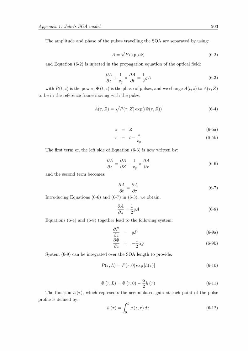
Appendix 1: Jahn’s SOA model 203
The amplitude and phase of the pulses travelling the SOA are separated by using:
A =√P exp(iΦ) (6-2)
and Equation (6-2) is injected in the propagation equation of the optical field:
∂A
∂z+
1
vg× ∂A
∂t=
1
2gA (6-3)
with P (t, z) is the power, Φ (t, z) is the phase of pulses, and we change A(t, z) to A(τ, Z)
to be in the reference frame moving with the pulse:
A(τ, Z) =√P (τ, Z) exp(iΦ(τ, Z)) (6-4)
z = Z (6-5a)
τ = t− z
vg(6-5b)
The first term on the left side of Equation (6-3) is now written by:
∂A
∂z=∂A
∂Z− 1
vg× ∂A
∂τ(6-6)
and the second term becomes:
∂A
∂t=∂A
∂τ(6-7)
Introducing Equations (6-6) and (6-7) in (6-3), we obtain:
∂A
∂z=
1
2gA (6-8)
Equations (6-4) and (6-8) together lead to the following system:
∂P
∂z= gP (6-9a)
∂Φ
∂z= −1
2αg (6-9b)
System (6-9) can be integrated over the SOA length to provide:
P (τ, L) = P (τ, 0) exp [h(τ)] (6-10)
Φ (τ, L) = Φ (τ, 0)− α
2h (τ) (6-11)
The function h (τ), which represents the accumulated gain at each point of the pulse
profile is defined by:
h (τ) =
∫ L
0g (z, τ) dz (6-12)
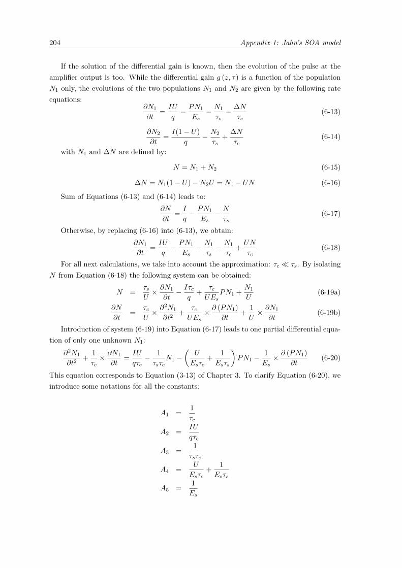
204 Appendix 1: Jahn’s SOA model
If the solution of the differential gain is known, then the evolution of the pulse at the
amplifier output is too. While the differential gain g (z, τ) is a function of the population
N1 only, the evolutions of the two populations N1 and N2 are given by the following rate
equations:∂N1
∂t=IU
q− PN1
Es− N1
τs− ∆N
τc(6-13)
∂N2
∂t=I(1− U)
q− N2
τs+
∆N
τc(6-14)
with N1 and ∆N are defined by:
N = N1 +N2 (6-15)
∆N = N1(1− U)−N2U = N1 − UN (6-16)
Sum of Equations (6-13) and (6-14) leads to:
∂N
∂t=I
q− PN1
Es− N
τs(6-17)
Otherwise, by replacing (6-16) into (6-13), we obtain:
∂N1
∂t=IU
q− PN1
Es− N1
τs− N1
τc+UN
τc(6-18)
For all next calculations, we take into account the approximation: τc � τs. By isolating
N from Equation (6-18) the following system can be obtained:
N =τsU× ∂N1
∂t− Iτc
q+
τcUEs
PN1 +N1
U(6-19a)
∂N
∂t=
τcU× ∂2N1
∂t2+
τcUEs
× ∂ (PN1)
∂t+
1
U× ∂N1
∂t(6-19b)
Introduction of system (6-19) into Equation (6-17) leads to one partial differential equa-
tion of only one unknown N1:
∂2N1
∂t2+
1
τc× ∂N1
∂t=IU
qτc− 1
τsτcN1 −
(U
Esτc+
1
Esτs
)PN1 −
1
Es× ∂ (PN1)
∂t(6-20)
This equation corresponds to Equation (3-13) of Chapter 3. To clarify Equation (6-20), we
introduce some notations for all the constants:
A1 =1
τc
A2 =IU
qτc
A3 =1
τsτc
A4 =U
Esτc+
1
Esτs
A5 =1
Es
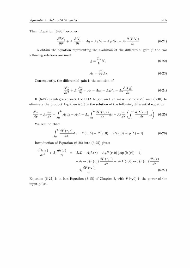
Appendix 1: Jahn’s SOA model 205
Then, Equation (6-20) becomes:
∂2N1
∂t2+A1
∂N1
∂t= A2 −A3N1 −A4PN1 −A5
∂ (PN1)
∂t(6-21)
To obtain the equation representing the evolution of the differential gain g, the two
following relations are used:
g =Γa
VN1 (6-22)
A6 =Γa
VA2 (6-23)
Consequently, the differential gain is the solution of:
∂2g
∂t2+A1
∂g
∂t= A6 −A3g −A4Pg −A5
∂(Pg)
∂t(6-24)
If (6-24) is integrated over the SOA length and we make use of (6-9) and (6-10) to
eliminate the product Pg, then h (τ) is the solution of the following differential equation:
d2h
dτ+A1
dh
dτ=
∫ L
0A6dz −A3h−A4
∫ L
0
dP (τ, z)
dzdz −A5
d
dτ
(∫ L
0
dP (τ, z)
dzdz
)(6-25)
We remind that:∫ L
0
dP (τ, z)
dzdz = P (τ, L)− P (τ, 0) = P (τ, 0) [exp (h)− 1] (6-26)
Introduction of Equation (6-26) into (6-25) gives:
d2h (τ)
dτ2+A1
dh (τ)
dτ= A6L−A3h (τ)−A4P (τ, 0) [exp (h (τ))− 1]
−A5 exp (h (τ))dP (τ, 0)
dτ−A5P (τ, 0) exp (h (τ))
dh (τ)
dτ
+A5dP (τ, 0)
dτ(6-27)
Equation (6-27) is in fact Equation (3-15) of Chapter 3, with P (τ, 0) is the power of the
input pulse.

206 Appendix 2: Agrawal’s SOA model
Appendix 2: Agrawal’s SOA model

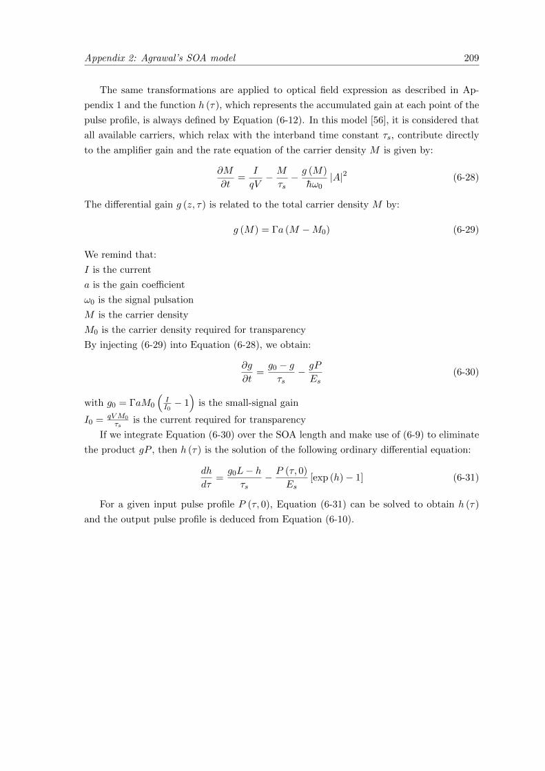
Appendix 2: Agrawal’s SOA model 209
The same transformations are applied to optical field expression as described in Ap-
pendix 1 and the function h (τ), which represents the accumulated gain at each point of the
pulse profile, is always defined by Equation (6-12). In this model [56], it is considered that
all available carriers, which relax with the interband time constant τs, contribute directly
to the amplifier gain and the rate equation of the carrier density M is given by:
∂M
∂t=
I
qV− M
τs− g (M)
hω0|A|2 (6-28)
The differential gain g (z, τ) is related to the total carrier density M by:
g (M) = Γa (M −M0) (6-29)
We remind that:
I is the current
a is the gain coefficient
ω0 is the signal pulsation
M is the carrier density
M0 is the carrier density required for transparency
By injecting (6-29) into Equation (6-28), we obtain:
∂g
∂t=g0 − gτs
− gP
Es(6-30)
with g0 = ΓaM0
(II0− 1)
is the small-signal gain
I0 = qV M0
τsis the current required for transparency
If we integrate Equation (6-30) over the SOA length and make use of (6-9) to eliminate
the product gP , then h (τ) is the solution of the following ordinary differential equation:
dh
dτ=g0L− hτs
− P (τ, 0)
Es[exp (h)− 1] (6-31)
For a given input pulse profile P (τ, 0), Equation (6-31) can be solved to obtain h (τ)
and the output pulse profile is deduced from Equation (6-10).

210 Appendix 3: Publications

Appendix 3: Publications

Appendix 3: Publications 213
1. V. Roncin, S. Lobo, M. N. Ngo, L. Bramerie, A. O’Hare, M. Joindot, and J.-C.
Simon, “Patterning effects in All-Optical Clock recovery: Novel Analysis using a clock
remodulation technique,” Journal of selected topics in quantum electronics, vol. 16,
no. 5, pp. 1495–1502, 2010.
2. M. N. Ngo, Q. T. Le, V. Roncin, M. Gay, L. Bramerie, and J.-C. Simon, “Etude
numerique de l’impact du filtrage optique sur les proprietes regeneratives d’un con-
vertisseur de longueur d’onde interferometrique en configuration differentielle,” in
Journees Nationales d’Optique Guidee, Lille, France, 2009, p. A10.2.
3. M. N. Ngo, M. Gay, L. Bramerie, G. Girault, Q. T. Le, J.-C. Simon, R. Brenot, G.-H.
Duan, D. Reid, and L. Barry, “Characterisation of semiconductor optical amplifiers for
all-optical regeneration,” in 5th Optoelectronic and Photonic Winter School, CMOS
Photonics, Trento, Italia, 2009.
4. M. N. Ngo, V. Roncin, Q. T. Le, L. Bramerie, D. Chevallier, L. Lablonde, A. Shen,
G.-H. Duan, and J.-C. Simon, “Bit-Error-Rate Performance Enhancement of All-
Optical Clock Recovery at 42.66 Gb/s Using Passive Prefiltering,” IEEE Photonics
Technol. Lett., vol. 20, no. 18, pp. 1557–1559, 2008.
5. M. N. Ngo, M. Gay, L. Bramerie, G. Girault, Q. T. Le, J.-C. Simon, R. Brenot, G.-
H. Duan, D. Reid, and L. Barry, “Characterisation of semiconductor optical amplifiers
for all-optical regeneration,” in International workshop on photonics and applications,
Nha Trang, Vietnam, 2008, p. B35.
6. M. N. Ngo, V. Roncin, Q. T. Le, S. Lobo, M. Gay, L. Bramerie, J.-C. Simon, A. Shen,
and G.-H. Duan, “High Performance and Polarisation-Insensitive BER Assessment
of a 42.66 Gbit/s All-Optical Clock Recovery,” in European Conference on Optical
Communications, Brussels, Belgium, 2008, p. Mo.3.C.6.
7. M. N. Ngo, V. Roncin, Q. T. Le, L. Bramerie, D. Chevallier, L. Lablonde, A. Shen,
G.-H. Duan, and J.-C. Simon,“Amelioration de la qualite d’une recuperation d’horloge
tout-optique en utilisant un filtrage passif,” in Journees Nationales d’Optique Guidee,
Lannion, France, 2008, p. Ma.3.6.
8. M. N. Ngo, V. Roncin, Q. T. Le, S. Lobo, M. Gay, L. Bramerie, A. Shen, G.-
H. Duan, and J.-C. Simon, “Caracterisation de dispositifs de recuperation d’horloge
tout-optique par la mesure de taux d’erreur binaire,” in Journees Nationales d’Optique
Guidee, Lannion, France, 2008, p. A.5.2.
9. J. C. Simon, M. Gay, L. Bramerie, V. Roncin, M. Joindot, T. Chartier, Lobo, G. Gi-
rault, Q. T. Le, T. N. Nguyen, and M. N. Ngo, “Long Distance Transmission Using
Optical Regeneration,” in Optical Fiber Communication Conference, San Diego, Cal-
ifornia, 2008, p. OWS1.

214 Appendix 3: Publications
10. M. N. Ngo, G. Girault, J.-C. Simon, and V. Roncin, “Utilisation du melange a
quatre ondes dans une fibre optique pour la creation d’une source impulsionnelle
accordable synchronisee sur un train d’impulsions maıtre,” in Journees Nationales
d’Optique Guidee, Grenoble, France, 2007, p. P8.
11. G. Girault, M. N. Ngo, D. Delubac, J.-C. Simon, and V. Roncin, “Analyse de la
sensibilite a la polarisation de SOA utilises en conversion de longueur d’onde,” in
Journees Nationales d’Optique Guidee, Grenoble, France, 2007, p. ME5.

Resume
Face a l’augmentation constante du trafic lie notamment a Internet, la demande de ca-
pacite dans les reseaux coeur ne cesse de croıtre : le debit par canal des systemes WDM a
atteint 40 Gbit/s et va bientot atteindre 100 Gbit/s et 160 Gbit/s. A partir de 40 Gbit/s, le
traitement tout-optique du signal peut offrir une solution interessante pour reduire la con-
sommation ainsi que le cout des systemes optiques du futur. L’objectif de cette these est
de developper des portes optiques non-lineaires et d’explorer des methodes de recuperation
d’horloge optique, toutes a base des semiconducteurs, pour la regeneration tout-optique de
signaux a un debit egal ou superieur a 40 Gbit/s. La dynamique ultrarapide du gain des am-
plificateurs optiques a semiconducteurs (SOA) est etudiee afin de l’exploiter pour developper
des fonctions simples et compactes permettant la remise en forme du signal. Concernant
la fonction de resynchronisation, differentes recuperations d’horloge tout-optiques ont ete
etudiees dans cette these.
La premiere partie des travaux a ete consacree entierement aux portes optiques non-
lineaires a base des SOA pour des applications a la regeneration 2R. L’experience pompe-
sonde permettant mesurer le temps de recuperation du gain a ete realisee pour etudier la
dynamique des SOA. Dans cette these, il a ete demontre que le SOA massif a fort confine-
ment et le SOA ultra-long a boıtes quantiques sont les plus adaptes pour un fonctionnement
a 40 Gbit/s avec des temps de recuperation du gain respectivement de 20 ps et 10 ps. Les
etudes experimentales ainsi que numeriques ont mis en evidence la contribution importante
des effets intrabandes a la dynamique du gain lorsque des SOA sont satures par des im-
pulsions courtes (quelques picosecondes). Le SOA massif de fort confinement a ete associe
avec un absorbant saturable (SA) pour constituer une fonction de regeneration 2R com-
plete. L’efficacite du regenerateur SOA-SA pour la remis en forme du signal a 40 Gbit/s a
ete demontree experimentalement and numeriquement.
La deuxieme partie des travaux a ete dediee a la recuperation d’horloge a base de lasers
auto-pulsants en vue d’une application a la regeneration 3R a 40 Gbit/s. Nous avons pro-
pose une technique originale pour evaluer la performance des fonctions de recuperation
d’horloge, qui consiste a remoduler l’horloge recuperee. Une nouvelle configuration a ete
elaboree pour ameliorer la qualite de l’horloge recuperee par le laser auto-pulsant a base de
materiau massif. Elle consiste a introduire un pre-filtrage passif devant le laser. La sensi-
bilite a la polarisation des recuperations d’horloge a ete egalement etudiee. La recuperation
d’horloge utilisant le laser massif suivi par le laser a boıtes quantiques a montre son insen-
sibilite a la polarisation du signal injecte par la mesure du taux d’erreur binaire. Enfin,
une etude preliminaire sur la tolerance des recuperations d’horloge a la dispersion modale
de polarisation a ete menee.
Mots-cles : amplificateurs optiques a semiconducteurs, lasers auto-pulsants a semicon-
ducteurs, recuperation d’horloge optique, regeneration tout-optique
Abstract
The optical backbone networks are facing a continuous and tremendous growth of the
Internet traffic, requiring to increase the capacity of the transmission systems: WDM sys-
tems with a bit rate of 40 Gbit/s do exist and 100 Gbit/s and 160 Gbit/s will be reached
soon. At the bit rates of 40 Gbit/s and higher, all-optical signal processing techniques
are a very interesting approach in order to reduce the power consumption and the cost
of future optical networks. The objective of this work is to develop non-linear optical
gates and explore Optical Clock Recovery (OCR) functions based on semiconductor tech-
nology for all-optical regeneration at 40 Gbit/s and above. The non-linear dynamic gain of
Semiconductor Optical Amplifiers (SOA) was investigated in order to perform simple and
compact signal reshaping devices. For retiming function, several OCR configurations based
on Self-Pulsating (SP) lasers were investigated during this thesis.
The first part of this work is devoted to the SOA-based non-linear optical gates for
all-optical 2R regeneration. Gain dynamics assessments using the pump-probe experiment
were performed to measure the SOA recovery time. In this work, it is demonstrated that the
highly confined bulk based SOA and the long quantum-dot based SOA exhibiting respec-
tively gain recovery times of 20 ps and of 10 ps are suitable for 40 Gbit/s operation. The
numerical and experimental studies clarified the important role of intraband effects in SOA
dynamics under short pulse (a few of picoseconds) saturations, which makes these SOAs
compatible for ultrahigh bit rate operations. The highly confined bulk based SOA was cas-
caded with a Saturable Absorber (SA) to constitute a complete 2R regeneration function.
The reshaping capability of the SOA-SA regenerator has been successfully demonstrated at
40 Gbit/s by experiments and simulations.
The second part of this work explores some clock recovery functions based on SP lasers
for 3R regeneration at 40 Gbit/s. An original characterisation technique consisting in re-
modulating the extracted clock was proposed to evaluate the OCR performance. A simple
solution using passive pre-filtering was developed to enhance the clock quality extracted by
a bulk based SP laser. The polarisation sensitivity of various OCR devices was evaluated.
The OCR based on the bulk based SP laser followed by the quantum-dot based SP laser
exhibits a total insensitivity to the arriving signal polarisation thanks to Bit-Error-Rate
measurements. At last, a preliminary study was devoted to investigate OCR tolerance to
Polarisation Mode Dispersion (PMD).
Key words: semiconductor optical amplifiers, self-pulsating semiconductor lasers, opti-
cal clock recovery, all-optical regeneration