Embed Size (px)
Citation preview

74
The transistor.
We have already discussed the physical principles behind the operation of the bipolar
junction transistor and so we will now move on to show how it can be used in both
digital and analogue circuits. We know that the bipolar junction transistor is a three
layer structure consisting of a sandwich of p and n type semiconductors. It is a three
terminal device with connections to the two outer layers as well as to the central
control region. There are two possible arrangements, npn and pnp. We shall
concentrate on the npn type although our general conclusions apply equally to the pnp
device except that the polarities of the voltages and currents must be reversed. The
basic npn device together with its circuit symbol is show below.
The arrow on the emitter indicates that the transistor is an npn device. The symbol for
a pnp transistor is similar except that the direction of the arrow is reversed. As we
know the structure looks rather like two pn junctions connected back to back with a
common intermediate connection called the base terminal.
Although the structure resembles two pn junctions the common base region is made
sufficiently thin so as to lead to behaviour which is completely different from that
n
p
n
Collector
Emitter
Base
E
I C
I E
I BB
C
C
B
E
75
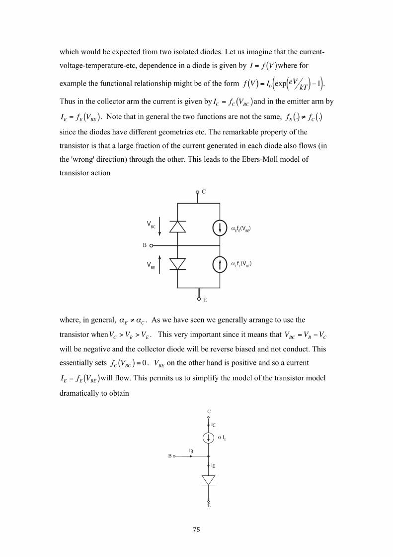
which would be expected from two isolated diodes. Let us imagine that the current-
voltage-temperature-etc, dependence in a diode is given by
€
I = f V( )where for
example the functional relationship might be of the form
€
f V( ) = I0 exp eV kT( ) −1( ). Thus in the collector arm the current is given by
€
IC = fC VBC( )and in the emitter arm by
€
IE = fE VBE( ). Note that in general the two functions are not the same,
€
fE .( ) ≠ fC .( )
since the diodes have different geometries etc. The remarkable property of the
transistor is that a large fraction of the current generated in each diode also flows (in
the 'wrong' direction) through the other. This leads to the Ebers-Moll model of
transistor action
where, in general,
€
αE ≠αC . As we have seen we generally arrange to use the
transistor when
€
VC >VB >VE . This very important since it means that
€
VBC =VB −VC
will be negative and the collector diode will be reverse biased and not conduct. This
essentially sets
€
fC VBC( ) = 0 .
€
VBE on the other hand is positive and so a current
€
IE = fE VBE( )will flow. This permits us to simplify the model of the transistor model
dramatically to obtain
C
B
E
!EfE(VBE)
!CfC(VBC)
VBC
VBE
BIB
IE
IC
C
E
! "E

76
where we have written
€
αE =α which, as we have seen, usually has a value very close
to unity, 0.98 or 0.99 being typical values. The equations describing the transistor are
essentially
€
IE = fE VBE( ) ≈ I0 exp eVkT
−1
IC = α IE
There must of course be current balance and so
€
IB + IC = IE . Alternatively we can
substitute
€
IE = IC α and so obtain
€
IC =α1−α
IB = βIB
where β is the current gain of the transistor which of course depends on the material
properties of the semiconductors and the device geometry. It's value can vary
dramatically from transistor to transistor and lies in the range 50 -200. We often take
100 as a typical value. However the important point is, as we have seen, that the
collector current is directly proportional to the base current and so we can think of the
device as being 'current controlled'.
The basic properties of the BJT may be summarised as follows.
(i) When the base-emitter junction is forward biased it drops a nominal voltage of,
say, 0.6 V for a silicon pn junction.
(ii) Since the base-collector junction is reverse biased
€
IC is almost independent of
€
VBC .
(iii)
€
IC is an exponential function of
€
VBEand directly proportional to
€
IB .
These properties are illustrated on the characteristics below. The relationship between
€
IB and VBE may be regarded as the input characteristics and that between
€
IC and VCE
as the output characteristics. We note that there is a very weak VCE dependence of the
input characteristics but that disappears for VCE greater than about one volt. We also
note that it is conventional to relate all voltages to that of the emitter.

77
It is clear that the
€
IB /VBE characteristics are essentially independent of VCE for VCE
greater than about one volt, at which time it is reasonable to set VBE ~0.6 V for all IB.
Similarly it is clear that for VCE greater than about one volt the IC characteristics are
essentially independent of VCE and that IC is directly proportional to IB ,
€
IC − βIB .
This permits us to simplify the characteristics to
0.5 mA5 V
20 V
I B
1 VVBE0
VCE
0 2 4 6 8 10 12
10
20
30
050
100
150
200
250
I B = 300I C (mA)
0VCE
!A
IB
VBE0
IC
VCE
0.6 V
for all VCE
0.5V, say
IB
IC = ! IB

78
A simple transistor circuit.
Consider the following circuit and suppose that we want to know how Vout changes as
VS varies between -10 and +10 Volts. We'll also assume that β = 100 and that VCE >
1.0V.
It is clear from our previous discussion that transistor action does not begin, i.e. the
transistor does not switch on, until VBE reaches 0.6V. VBE thereafter remains fixed at
0.6V. Thus
€
−10 <VS < 0.6 IB = IC = 0 and Vout = 20
VS > 0.6V IB =VS − 0.6
100mA and IC = β
VS − 0.6100
mA
and
€
Vout = 20 − 5IC = 20 − 5β VS − 0.6100
However neither IC or Vout can increase indefinitely. The limit is set by the maximum
value IC can take which is determined primarily by the 5 kΩ load resistor, the supply
voltage and the requirement that VCE > 1V. The limit is therefore given by
5 k!
VS
100 k!
Vout
20V
VBE
IC
IB

79
IC MAX =
€
20 −15
mA = 3.8mA. Any further increase would make the transistor appear
to be a source of energy whereas, of course, all the transistor can actually do is to act
as a variable obstruction to current flow.
The limit of IC = 3.8 mA occurs when VS = 4.4V (β = 100). Thus we may write
€
0.6 <VS < 4.4 Vout = 23− 5VS
and
€
dVout
dVS = − 5
and so, in this region it is reasonable to regard the circuit as an amplifier with gain of
minus 5.
Outside this range IC is either zero – the transistor is cut-off – or limited by the 5 kΩ
resistor --the transistor is saturated --and so could be used as a voltage controlled
SWITCH.
Let's now analyse the circuit again graphically with the aid, this time, of our idealised
characteristics. We know that when the transistor is switched on
€
20 = 5IC +VCE or IC = 4 − VCE5
20
1.0
0.6VS
active (linear)
cut-off
saturated
Vout
4.4

80
We can superimpose this load line on the transistor characteristics in just the same
way that we did for the diode case.
It is clear that as IB increases from zero the values of (IC, VCE) are given by the
intersection of the load line with the horizontal characteristic corresponding to the
particular value of IB of interest. Consequently (IC, VCE) varies from (0, 20V) at point
A to (3.8 mA, lV) at point B.
The transistor switch --the inverter.
It is probably fair to say that more transistors are used as switches in computers and
calculators than are used as linear amplification deices, such as in hi-fi amplifiers and
radios. The fundamental switching circuit is actually the one we have just discussed
and is often called an inverter for reasons which will become apparent.
I C
1V 20V VCE
A
4mA
IB = 38 !AB
RB
RC
0 Input Output
E
VHIE

81
When the input to the circuit is low, 0V, the transistor is switched off, no current
flows and V0 = 20V. On the other hand when the input is high, RB and RC are chosen
such that the maximum possible collector current flows, i.e. the transistor is saturated.
This sets V0 = 0V (if we neglect the small vCE drop). If we set VHI=E then the output
pulse is simply an inverted form of the input pulse -- hence the name.
In terms of the load line construction the change in state of the input corresponds to
an abrupt change in operating point from A (off) to B (on).
I C
VCE
B
A
IB when transistor ‘on’

82
The BJT as an amplifier.
Our intention is to build an amplifier which will be capable of amplifying small a.c.
signals. These signals can be thought of as containing many sinusoidal components
such as
€
vin t( ) = asin ωt( ). Unfortunately, as we have just seen, our transistor cannot
cope with negative signals --it cuts off and transistor action ceases. The way around
this is to bias the transistor by introducing a constant input so as to set a dc output
level somewhere in the middle of the active range of transistor action so that a small
ac waveform can be superimposed on it without the transistor becoming cut-off. The
output will now take the form
€
vout =V0 + Asin ωt( )
where V0 is the constant output voltage caused by the biasing. It is also referred to as
the operating point or quiescent point of the transistor. The small ac signal
€
Asin ωt( )is
superimposed on this. As we have said VO (and a) must be chosen so that VO+a does
not drive the transistor into saturation and VO-a does not cause it to cut-off. Often a is
quite small and in any case, the biasing is usually designed so as to set VO roughly in
the middle of the output range.
We will now begin by discussing methods to reliably set the operating point, i.e. how
to bias the transistor (XIN and XOUT) before moving on to introduce simple techniques
to anaylse the small signal behaviour (xin and xout).
We shall follow the same general method that we developed for the diode to derive
simple relationships between (xin and xout).
XIN + xin sin !t XOUT + xout sin !t

83
Biasing --defining the operating point.
We recall that in order that the transistor operates in the active region it is necessary
that
(i) The base-emitter junction is forward biased so that a current flows into the base.
(ii) The collector-emitter voltage is sufficiently positive that the collector-base
junction is reverse biased.
If these conditions hold then
(iii) The base-emitter voltage is almost constant at -0.6V.
(iv)
€
IC is independent of
€
VCEand
€
IC = βIB .
These simplifications are equivalent to approximating the real characteristics by the
straight line versions we have already discussed. We can now think of biasing as
establishing steady state currents and voltages such that conditions (i) and (ii) are met.
We shall divide the biasing process into two parts. The first will deal with the input
requirements and the second with the output requirements. We shall concentrate on
the common emitter configuration we have already met (it is called common emitter
because the emitter can be thought of as being the common connection between the
input and the output). Let's now try and set condition (i).
Plan A. Why not use a constant voltage source to set VBE to the precise
value required to achieve conduction? This is not sensible because
(i) The exact value of VBE will vary from transistor to transistor.
(ii) IB and IC change very rapidly with VBE and so are likely to be ill defined.
(iii) If VBE really is set to be constant it would have the removing (effectively short-
circuiting) any signal voltage we attempted to impress on VBE ! Let's think again.

84
Plan B. Why not set IBand let VBE have whatever value it likes. The simple circuit
below gives
€
IB =V −VBE
RB
which, since VBE ~ 0.6V, can be well defined if V is large enough. This input biasing
has also set IC via IC = β IB. It now remains to set the collector voltage such that
condition (ii) is met. Again we cannot use a perfect voltage source since this would
effectively short-circuit any signal voltage developed at the collector. We note that we
may write VCE as
€
VCE = E − ICRC
We note that it is usually convenient to use the same supply voltage for the base and
collector currents and so V = E.
These steady state voltages and currents exist in the absence of any input signal. If a
small signal voltage is impressed on this quiescent value of VBE then the base current
will change and so will IC which, in its turn, will cause a change in the output voltage
developed across RC. This is easy to visualise from the load line construction shown
RCRB
IC
+V +E

85
below where we have superimposed the load line (equation above) on the device
characteristics
The quiescent operating point Q is determined by the biasing and lies at the
intersection of the load line with the transistor characteristic for the particular value of
current IB. As the input signal, IB, varies the operating point moves along the load
line. The corresponding changes in IC and VBE can be obtained by projection from the
current and voltage axes. The relationship between the input voltage, VBE and the
input current, IB, can also be seen graphically as shown below.
If the output signal is relatively small then the exact position of Q is not important.
However as we have said before we usually try to position it roughly in the middle of
the output range so as to allow for large output swings and also biasing tolerances, i.e.
we might not get the quiescent point exactly right in practice!
Having said all this I am rather reluctant to admit that this biasing plan is also a bad
idea. It relies on defining IC via IB and we know that this is a rather unreliable
parameter which varies from transistor to transistor. The operating point is not well
defined by this approach and we should try to do better.
Plan C. Since IC is what we are actually trying to set why don't we stop messing
around and try to devise a circuit which would set IC and VCE directly rather than in
some indirect manner. The ideal circuit should be insensitive to any device parameter
which is likely to be ill-defined as well as to temperature. As you might reasonably
imagine many people have given a good deal of thought to this problem and the
I B
IC
VCE
Q

86
circuit we show below is pretty much the standard method of biasing single stage
amplifiers.
The improved circuit provides nearly constant base voltage by potential division from
a reference source, usually E. This means that the emitter voltage is well defined since
VBE is nearly constant. This then gives the emitter current as
€
IE =VE
RE
=VE −VBE
RE
Also
€
IE = IB + IC and
€
IC = βIB and so
€
IC = β1+ β
IE ≈ IE since β is large.
In order to analyse the circuit further let's replace the potential divider by it's
Thevenin equivalent
RC
R2 RE
R1
IC
IE
E

87
where
€
VT =R2
R1 + R2
E and RT = R1R2
R1 + R2
We can now write
€
VT = IBRT +VBE + ICRE
and hence the collector current is given by
€
IC =VT −VBE
RE + RT β
For large β and a proper choice of RT (R1 and R2) and RE , we can arrange that
€
RE >> RT β and hence make IC independent of β.
€
IC =VT −VBE
RE
We now re-write the loop equation for VT above as
RC
RE
IC
IE~IC
E
RT
VT
IB

88
€
VT = IBRT + ICRE +VBE
= ICRTβ
+ RE
+VBE
and see that our decision to set
€
RE >> RT β is equivalent to ignoring the voltage drop
across RT due to the very small base current. Further we can simplify the equation to
€
VT = ICRE +VBE = VE +VBE = VB
which is to be expected as our choice of
€
RE >> RT β is, as we have said, equivalent to
ignoring the small voltage drip across RT.
Finally
€
VCE = E − ICRC −VE
An aside. Although it is not obvious from the above discussion this circuit also
compensates for variations in VBE from device to device or due to temperature
change. We can get a rough idea about operating point 'stability' by differentiating to
obtain
€
dICdβ
=RT VT −VBE( )βRE + RT( )2
and
€
dICdVBE
=−1
RE + RT /β( )
Good stability is achieved if RE and β are high and RT is low.
Another Aside. This may well be the first circuit you have met where negative
feedback --an extremely powerful technique of which you will learn a great deal more
later -- has been used. The resistor, RE, has been used to 'feed back' information about
the output circuit, IC, IE etc. to the input circuit.

89
The base-emitter voltage may be regarded as the input voltage minus a sample of the
output,
€
IERE ≈ ICRE . If , for example, the transistor were to be replaced by one with a
lower β then IC, IE, and VE will fall. However since VT is held constant the fall in VE
will be compensated by an increase in VBE and hence IB. Thus IC recovers to a level
very close to the original.
Choosing the bias resistors --circuit design.
If values are given for the resistors then it is easy to determine the operating point. It
is less easy, but more fun, to choose the values, i,e. to design the circuit since
compromises have to be made and so there are often more than one set
of resistor values which will result in acceptable performance. As an example let's
assume that we want to choose R1, R2, RE and RC so as to set the operating point
nominally at IC = 2mA, VCE = 7V and E = 12V for a transistor with a minimum
current gain, β, of 100.
Since we want to make the base voltage as well defined as possible let's begin by
allowing, say, a l V drop across RE. This is probably reasonable since it won't
dramatically reduce the output swing and is also sufficiently large to swamp any
variations in VBE from transistor to transistor so that VT -VBE is reasonably constant.
RC
RE
12 V
RT
VT
2 mA
7 V

90
This choice of emitter voltage allows us to calculate RE and RC remembering, IC = IE,
as
€
RE = 500 Ω
and
€
RC = 12 − 7 −1( ) /2mA = 2 kΩ
We also know that VB = 1+0.6 = 1.6V if we assume VBE = 0.6. It now remains to find
Rl and R2.
We recall from our previous analysis that
€
IC =VT −VBE
RE + RT β
which will be reasonably independent of β if we choose, say, RE, > 10RT/β. In our
case we will set RT = 10 RE = 5 kΩ. It now remains to find Rl and R2.
We now have one equation relating the two resistors R1 and R2 via, RT = 5 kΩ but we
still need another. We may obtain this equation, in the spirit of our approximation by
setting VT = VB as we have already discussed. Our two equations are now
€
VT =R2
R1 + R2
12 = VB = 1.6 V and RT = R1R2
R1 + R2
= 5 kΩ
from which we find
€
R1 = 37.5 kΩ and
€
R2 = 5.7 kΩ. The closest standard values of
resistor available would suggest that we might choose Rl = 36 kΩ (37.5), R2 = 5.6 kΩ
(5.7), RE= 510 Ω, (500) and RC = 2 Ω (2). This gives rise to IC = 1.82 mA rather than
the nominal value of 2mA. Why is this so different and does it matter? The main
reasons are that we took RE = 10 RT and so we were prepared to accept a 10% ish
error in the analysis. We also ignored the base current. It's not too surprising then that
if we use the actual design values we chose in a rigorous circuit calculation that we
won't get quite the nominal values we aimed for. Whether the discrepency matters or
not depends on the application. In most cases a design values such as those we have
obtained are perfectly acceptable.

91
We emphasise that this is not a unique solution and that the design of circuits and the
choice of component values is not an exact science. The resistors we use will all have
tolerances as will the transistor parameters. It doesn't matter if the actual operating
point isn't exactly at the nominal point since for small signals the swings are unlikely
to cause the transistor either to cut-off or to saturate. We have tried to present a
plausible design philosophy. Naturally many other people have considered the
problem and another rule of thumb which has been found to provide well behaved
circuits is to set
€
VE = 0.1E
R2 =βRE
10
This approach gives, if we again ignore the base current, RE = 600 W , RC = 1.9 kΩ
and Rl = 34 kΩ which gives substantially similar component values to the ones found
from our design.