Embed Size (px)
Citation preview
MAY 2010
AUTOMOTIVE EMC LABORATORY RECOGNITION PROGRAM
EMC andRAILWAY SAFETY
A DASH OF MAXWELL’SA Maxwell’s Equations Primer
Part 5
CDM Currents forSMALL INTEGRATED CIRCUITS
The “Real” Cost ofESD DAMAGE
MagazineTHE COMPLIANCE INFORMATION RESOURCE FOR ELECTRICAL ENGINEERS
The Requirements of the
IN Compliance MagazinePO Box 235Hopedale, MA 01747CHANGE SERVICE REQUESTED
May 2010 IN Compliance 3
Lorie NicholsPublisher & Editor
Erin C. FeeneyDirector of Media Services
Sharon SmithDirector of Sales
Barbara KovalchekMedia Consultant
Magazine
IN Compliance MagazineISSN 1948-8254 (print)
ISSN 1948-8262 (online)
is published by
Same Page Publishing LLCP.O. Box 235
Hopedale, MA 01747tel: (508) 488-6274fax: (508) 488-6114
IN Compliance Magazine subscriptions within North America are $24.95 per year (12 issues). Subscriptions
outside North America are $124.95 per year (12 issues). The Digital Edition is free.
Please contact our circulation department at [email protected]
For information about advertising with IN Compliance, please call 978-760-0093 or
e-mail [email protected].
Copyright 2010 IN Compliance Magazine, all rights reserved.Contents may not be reproduced in any form without the prior consent of the publisher.
While every attempt is made to provide accurate information, neither the publisher nor the authors accept any liability for errors or omissions.
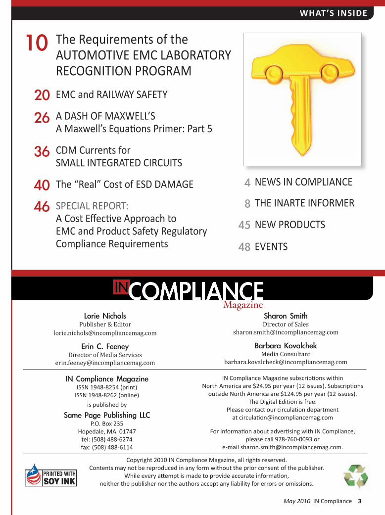
WHAT’S INSIDE
20 EMC and RAILWAY SAFETY
A DASH OF MAXWELL’S A Maxwell’s Equations Primer: Part 5
CDM Currents for SMALL INTEGRATED CIRCUITS
The “Real” Cost of ESD DAMAGE
SPECIAL REPORT: A Cost Effective Approach to EMC and Product Safety Regulatory Compliance Requirements
The Requirements of the AUTOMOTIVE EMC LABORATORY RECOGNITION PROGRAM
10
EVENTS48
NEWS IN COMPLIANCE4
THE INARTE INFORMER8
NEW PRODUCTS45
26
36
4046
4 IN Compliance May 2010 www.incompliancemag.com
NEWS IN COMPLIANCE
EU Commission Releases Recent RAPEX Stats on Unsafe Consumer ProductsThe Commission of the European Union (EU) has released statistics for February 2010 on notices of unsafe consumer products that have been processed through the EU’s rapid information system (RAPEX).
According to the Commission’s report, 323 notifications of unsafe products were received through the RAPEX system during the month. This is almost double the number of notifications received one year ago in February 2009, when the RAPEX system recorded just 163 notifications.
Of the 323 notifications received, 71 were related to the product category of toys (25%), and 33 were related to electrical appliances (12%). There were also 20 notifications related to unsafe motor vehicles, accounting for 7% of the total notifications.
Regarding the country of origin identified in connection with unsafe products, more than half (190 notifications, or 68%) of all notifications were related to products originating from China, including Hong Kong. Another 39 notifications (14%) of unsafe products originated in EU Member States. Eleven notifications (4%) failed to identify any country of origin.
To view the complete text of the Commission’s most recent report on RAPEX statistics, go to http://ec.europa.eu/consumers/safety/ rapex/docs/stat_02-2010.pdf.
EU Commission Revises Standards List for EMC DirectiveThe Commission of the European Union (EU) has published an updated list of standards that can be used to demonstrate conformity with the essential requirements of the EU’s directive on electromagnetic compatibility (also known as the EMC Directive, 2004/108/EC).
The EMC Directive applies to “any apparatus or fixed installation” and regulates the “ability of equipment to function satisfactorily…without introducing intolerable electromagnetic disturbances to other equipment.”
The provisions of the EMC Directive do not apply to telecommunications terminal equipment, which is covered under the essential requirements of Directive 1999/5/EC (also known as the R&TTE Directive).
The updated list of CEN, CENELEC and ETSI standards that can be used to demonstrate compliance with the EMC Directive was published on March 19th in the Official Journal of the European Union, and replaces all previously published standards lists for the Directive.
The complete list of standards can be viewed at http://eur-lex.europa.eu/LexUriServ/LexUriServ.do?uri=OJ:C: 2010:071:0001:0016:EN:PDF.
Updated Standards List Published for EU’s Low Voltage DirectiveThe Commission of the European Union (EU) has published an updated list of standards that can be used to demonstrate conformity with the essential requirements of its directive relating to electrical equipment designed for use within certain voltage limits (2006/95/EC).
The Directive defines “electrical equipment” as any device designed for use with a voltage rating of between 50 and 1000 V for alternating current, and between 75 and 1500 V for direct current.
Exemptions to the provisions of the Directive are identified in Annex II, and include electrical equipment for radiology and medical purposes, plug and socket outlets for domestic use, electrical equipment used in explosive atmospheres, and certain other types of specialized electrical equipment.
The updated list of standards that can be used to demonstrate compliance with the Directive was published on March 19th, in the Official Journal of the European Union, and replaces all previously published standards lists.
The complete list of standards can be viewed at http://eur-lex.europa.eu/LexUriServ/LexUriServ.do?uri=OJ:C:2010:071:0017:0087:EN:PDF (note that the list runs 70 pages).
FCC Proposes National Broadband PlanAs expected, the Federal Communications Commission (FCC) has released a sweeping proposal to bring broadband Internet access to nearly 100 million additional Americans.
The FCC’s plan, entitled Connecting America: The National Broadband Plan, was mandated under the 2009 American Recovery and Reinvestment Act, and produced by an FCC task force. In brief, the FCC’s plan includes the following goals and recommendations: y Connect 100 million households to affordable 100-megabits-per-second service;
y Provide ultra-high-speed broadband of at least 1 gigabit per second to schools, hospitals and military installations;
y Free up 500 megahertz of spectrum for licensed and unlicensed use;
y Increase broadband adoption rates in the Unites States from 65% to more than 90%;
y Transition Universal Service Fund support from analog technologies to improving the digital infrastructure;
y Conduct market-based analyses of price, speed and availability to promote competition across the broadband ecosystem;
y Provide every first responder with access to a nationwide, wireless, interoperable public safety network.
According to the FCC, more than 80 million American adults and 13 million American children over the age of five do not have access to high-speed Internet connections at home.
A summary of the Commission’s National Broadband Plan is available at http://hraunfoss.fcc.gov/edocs_public/attachmatch/DOC-296858A1.pdf.
FCC Releases Consumer Broadband AppsIn connection with the release of its National Broadband Plan, the Federal Communications Commission (FCC) has also released its first mobile application for certain handheld devices.
May 2010 IN Compliance 5
NEWS IN COMPLIANCE
The FCC’s new Consumer Broadband Test measures broadband quality indicators such as speed and latency, and reports the information to consumers and to the FCC. The FCC’s tool is reportedly based on two popular broadband testing tools, the Ookla, Inc. Speed Test and the Network Diagnostic Tool (NDT) running on the Measurement Lab (M-Lab) platform.
A mobile version of the test is available for downloading to your Apple iPhone or other Android-compatible device through the Apple iPhone apps website (www.apple.com/iphone/apps-for-iphone), or the Android App Store (www.android.com/market).
A fixed-line version of the broadband test is available at www.broadband.gov.
Additional information about the FCC’s new broadband applications is available at http://hraunfoss.fcc.gov/edocs_public/attachmatch/DOC-296810A1.pdf.
FCC Makes Spectrum Dashboard AvailableThe Federal Communications Commission (FCC) has also announced the release of a beta version of its new Spectrum Dashboard, which it says will enable users to learn more about how portions of the electromagnetic spectrum are allocated and used.
According to a press release issued by the FCC, the new Spectrum Dashboard includes four components that allow users to:
y Browse spectrum bands: Users can search by spectrum range by browsing an interactive spectrum chart:
y Search for spectrum licenses: Users can search by name, geographic area or service;
y Produce maps of spectrum licenses: Users can produce maps that depict a geographic service area for individual licenses, the amount of spectrum that has been licensed in a given area, or the amount of spectrum licensed to an individual licensee;
y Export raw data: Users can download raw data from any search into spreadsheets for more complex analysis.
The FCC’s new spectrum dashboard is available at www.fcc.gov/spectrumdashboard.
Toy Importer Pays $2 Million Penalty, Enters Consent DecreeAn importer of children’s toys has agreed to pay a civil penalty of more than $2 million in connection with its alleged violations of federal safety laws.
According to the U.S. Consumer Product Safety Commission (CPSC), the consortium companies, Daiso Holding USA Inc., Daiso Seattle LLC of Seattle, WA, and Daiso California LLC of Hayward, CA, imported, distributed and sold toys with illegal levels of lead content, illegal levels of lead paint, small parts on toys intended for children
younger than three years old, and products lacking required warning labels.
In addition to a civil penalty of $2.05 million, Daiso has also entered into a consent decree. Under the terms of the consent decree, Daiso is prohibited from importing, directly or indirectly, any toy or other children’s product until it retains an independent product safety coordinator, who will:
1. Assist in the creation of a comprehensive product safety program;
2. Conduct a product audit of merchandise to determine testing and certification requirements; and
3. Develop and establish procedures for compliance and reporting.
CPSC Chairman Inez Tenenbaum called the settlement with Daiso a “landmark agreement,” and that it “sets a precedent for any firm attempting to distribute hazardous products to our nation’s children.”
More details regarding this action by the CPSC are available at www.cpsc.gov/cpscpub/prerel/prhtml10/10151.html.
CPSC Approves Final Rule on Factors in Civil PenaltiesThe U.S. Consumer Product Safety Commission (CPSC) has clarified its rules regarding the factors it can consider when seeking civil penalties in connection with the importation and/or sale of unsafe products.
DILBERT: © Scott Adams/Dist. by United Feature Syndicate, Inc. Reprinted with permission.
6 IN Compliance May 2010 www.incompliancemag.com
NEWS IN COMPLIANCE
Consistent with the provisions of the U.S. Consumer Product Safety Improvement Act (CPSIA), the Commission has approved a final rule that requires it to consider the following factors in determining the amount of civil penalties it may levy in connection with violations of CPSC laws:
1. The nature, circumstance, extent and gravity of the violations, including the nature of the product defect or the substance;
2. The appropriateness of the penalty in relation to the size of the business or of the person charged (including how to mitigate undue adverse impacts on small businesses); and
3. Other factors as the Commission deems appropriate.
These factors are in addition to other factors that the Commission is already required to consider, such as the severity of the risk of injury, the occurrence or absence of injury, and the number of defective products distributed.
In its announcement regarding the rule change, the CPSC also notes that the maximum penalty for each violation of CPSC rules is now $100,000 (up from just $8000 before the passage of the CPSIA), and $15 million for a related series of violations (up from $1.8 million).
Additional information regarding the CPSC ruling on civil penalty factors is available at http://www.cpsc.gov/cpscpub/prerel/prhtml10/10168.html.
Company Recalls Remote Control Fire Kits Due to Fire HazardDimplex North America of Ontario, Canada has issued a voluntary recall for about 700,000 of its remote control kits for electric fireplaces and stoves, manufactured in China.
According to a recall alert issued by the U.S. Consumer Product Safety Commission (CPSC), the plug-in wall unit for the remote control kits can overheat, posting a fire and burn hazard to consumers.
Dimplex says that it has received about 5000 reports of the plug-in wall units
overheating, including 19 reports of house damage, and one report of a house fire that resulted in “considerable” property damage.
The recalled remote control kits were sold with several brands of electric fireplaces, stoves and fireplace inserts in mass merchandise, home improvement, specialty fireplace and furniture retailers from January 1998 through December 2008 for between $200 and $1500.
To view the CPSC notice regarding this recall, go to www.cpsc.gov/cpscpub/prerel/prhtml10/10167.html.
Fire Hazard Leads to Recall of Mobile Power PacksTumi of South Plainfield, NJ has issued a voluntary recall for about 5000 of its mobile power packs, manufactured in China.
The mobile power packs are designed to provide simultaneous DC charges to as many as five small electronic devices, such as mobile phones, PDAs and MP-3 players.
According the U.S. Consumer Product Safety Commission (CPSC), the lithium-ion cells used in the mobile power packs can ignite or explode while charging, posing a fire hazard.
Tumi reports that it has received notice of two incidents of small fires associated with the mobile power packs during their initial charge. However, no injuries have been reported.
The recalled mobile power packs were sold through Tumi retail stores, department and specialty stores nationwide and at www.Tumi.com from August 2007 through March 2008 for about $135.
To view the CPSC notice regarding this recall, go to www.cpsc.gov/cpscpub/prerel/prhtml10/10169.html.
Overheated Loudspeakers Spurs Recall of Audio ReceiversThe Niles Audio Corporation of Miami, FL has voluntarily recalled about 3800 of its ZR-6 MultiZone-brand audio receivers, manufactured in China.
According to the U.S. Consumer Product Safety Commission (CPSC), a failure in the receiver’s internal components can cause connected loudspeakers to overheat and cause a fire, posing a fire hazard to consumers.
Niles reports that it has received notice of three incidents of connected loudspeakers overheating, but no cases of injuries to consumers.
The recalled audio receivers were sold by audio/video/home theatre custom installation professionals nationwide from July 2008 through November 2009 for about $2000.
To view the CPSC notice regarding this recall, go to www.cpsc.gov/cpscpub/prerel/prhtml10/10724.html.
Edmunds Announces $1 Million for Auto FixAutomotive website www.Edmunds.com has announced that it will soon launch a contest to identify the cause of unintended acceleration in motor vehicles.
The prize? A cool $1 million to anyone who can “demonstrate in a controlled environment a repeatable factor that will cause an unmodified new vehicle to accelerate suddenly and unexpectedly.”
According to a notice posted on the company’s web site on March 15th, Edmunds.com is currently drafting rules for the contest, and will post them on its website as they become available.
Edmunds says that “every car company” has received complaints from consumers regarding unintended acceleration, and that many incidents have not been fully addressed by product recalls. Rather than more NHTSA (National Highway Traffic Safety Administration) investigations, “Isn’t it a time to try a different approach?” they ask.
For more information about the Edmunds’ contest, go to www.edmunds.com/industry-car-news/unintended-acceleration-competition.html.

8 IN Compliance May 2010 www.incompliancemag.com
The iNARTE InformerProvided by the International Association for Radio, Telecommunications and Electromagnetics
HEADQUARTERS NEWSUnfortunately our administrator for the FCC Licensure side of our operation, Judy Sydow, has had to leave iNARTE in order to undergo a series of medical treatments. This has been a sudden decision and we all wish her a full and speedy recovery. While we recruit a replacement for Judy, anyone wanting to schedule any of the FCC examinations or ask any questions about the program can contact Jeameeka White at the iNARTE office ([email protected]).
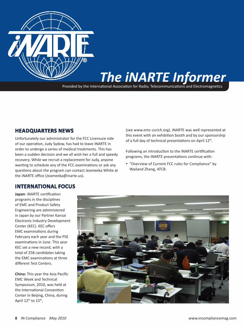
INTERNATIONAL FOCUSJapan: iNARTE certification programs in the disciplines of EMC and Product Safety Engineering are administered in Japan by our Partner Kansai Electronic Industry Development Center (KEC). KEC offers EMC examinations during February each year and the PSE examinations in June. This year KEC set a new record, with a total of 258 candidates taking the EMC examinations at three different Test Centers.
China: This year the Asia Pacific EMC Week and Technical Symposium, 2010, was held at the International Convention Center in Beijing, China, during April 12th to 15th,
(see www.emc-zurich.org). iNARTE was well represented at this event with an exhibition booth and by our sponsorship of a full day of technical presentations on April 12th.
Following an introduction to the iNARTE certification programs, the iNARTE presentations continue with:
y “Overview of Current FCC rules for Compliance” by Wailand Zhang, ATCB.

May 2010 IN Compliance 9
y “Introducing the new ANSI C63.10 Standards for Unlicensed Wireless Devices” by Michael Windler, Underwriters Labs.
y “Top 10 EMC Design Rules for Achieving Compliance” by Elya Joffe, K.T.M. Project Engineering.
Sponsoring and promoting such presentations and workshops is just a part of iNARTE’s dedication to providing opportunities for the professional development of all practitioners within the disciplines that we serve.
Singapore/Malaysia: This past twelve months has seen a significant increase in the number of applications for ESD certification in this region. The upsurge of interest can be attributed in great part to the excellent work of our partner in Singapore, who provides ESD control consulting services and training to the larger companies in that region.
NEW ESDA TRAINING COURSE AND CERTIFICATION OPPORTUNITIES:iNARTE and the Electrostatic Discharge Association, ESDA, have a formal agreement for mutual cooperation and promotion of awareness and engineering excellence in the control of electrostatic discharge. The ESDA has recently completed development of a two day, comprehensive short course, offering a broad exposure to the fundamentals of ESD Programs. This course will be offered for the first time at
the Doubletree Hotel on Chicago’s North Shore on June 16th and June 17th, followed by a one day tutorial on June 18th covering Electrostatic Calculations. On June 19th, attendees will have the opportunity to validate their knowledge of ESD Control by taking either the iNARTE ESD Certified Engineer examination, the iNARTE ESD Certified Technician examination or the ESDA Program Manager Certification examination.
Full details of this excellent opportunity for professional development and certification in ESD control can be found at www.esda.org/documents/June2010RTP.pdf.
Information on the application and registration procedures for either of the iNARTE ESD examinations can be found at www.narte.org/d/esdapp.pdf. Applicants can register with iNARTE on line and should enter “ESDA Workshop Chicago” as their selected Test Center.
Early registration is recommended to ensure space availability.
UPCOMING EVENTSSee the table below for upcoming events.
Several other workshops are in the pipeline, so be sure to visit the iNARTE web site regularly to be sure not to miss those in your region or field of interest. n
WHEN WHAT WHERE PARTNER/PRESENTER(s)
June 15 - 16 Workshop on ANSI C63.10 - 2009 Testing Unlicensed Wireless Devices
www.narte.org/h/ANSIC63.10Workshop.asp
Underwriters Laboratories
Northbrook, IL
Art Wall (Radio Regulatory Consultants)
Mike Windler (UL),
Bob Delisi (UL)
Bill Hurst (FCC)
June 16 - 19 Training Seminar covering ESD Program Essentials and Electrostatic Calculations, including Certification Examinations
www.esda.org/documents/June2010RTP.pdf
Doubletree Hotel and Conference Center
Chicago North Shore, IL
Ted Dangelmayer, (Dangelmayer Assoc.)
Dr Terry Welsher, (Dangelmauyer Assoc.)
Dr. Leo Henry, (Consulting Engineer)
Carl Newberg, (MicroStat Laboratories)
September 14 - 17
Laboratory Auditor ISO 17025 Training and Credentialing,
www.narte.org/d/ACLASS2010Flyer.pdf
Marriot O’Hare Airport
Chicago, IL
ANSI-ASQ National Accreditation Board, (ACLASS)
The Requirements of the
by Werner Schaefer Schaefer Associates
Automotive EMC Laboratory
Recognition Program
May 2010 IN Compliance 11
The Requirements of the AEMCLRP FEATURE
The Automotive EMC Laboratory Recognition Program (AEMCLRP) was established in 1998 by the three major automobile manufacturers in the United States,
Chrysler LLC (Chrysler), Ford Motor Company (Ford) and General Motors (GM). These companies formed a committee responsible for the definition, documentation and maintenance of a set of EMC tests that an accredited and recognized test laboratory may perform in order to determine the EMC characteristics of automotive components that are integrated in vehicles by the three manufacturers. Since 1998, the AEMCLRP requirements document has been reviewed several times, and revision 4 (with an addendum issued in May 2007), the most current revision, has been used for the past four years. Future revisions are to be expected, due to improvements identified during the assessment process, feedback of laboratories or changes in underlying EMC specifications.
In order for a test laboratory to be recognized by the three manufacturers, a process has to be completed that consists of two major steps. In the first step, the applicant laboratory has to seek accreditation from a recognized accreditation body (e.g., A2LA in the US or JAB in Japan). In order to be accredited, the laboratory must implement and operate a quality system that meets the requirements of ISO 17025-2005. In the technical area, the laboratory will have to identify the specific AEMCLRP tests for which it seeks accreditation. For all the tests, performance history data will have to be submitted prior to the actual on-site assessment for review by the assessor and the AEMCLRP committee. During the on-site assessment, all test methods the laboratory seeks accreditation for are reviewed. This includes an inspection of the actual test setup, verification of suitability of test equipment and the test environment, as well as technical interviews of staff members identified as being competent to perform specific tests. Upon resolution of any deficiencies identified during the on-site assessment, accreditation is granted by the accreditation body. The second step the laboratory has to complete is the performance of proficiency tests for some of the AEMCLRP tests. This involves the testing of an artifact the laboratory is provided with by the committee. This artifact has to be tested in accordance with the related test method, (e.g., Bulk Current Injection – BCI) and the test data has to be submitted to the accreditation body within 1 month after receiving the artifact. The accreditation body will forward the test data to the AEMCLRP committee for a technical review. Based on the review results, the applicant laboratory will be recognized by the individual members of the AEMCLRP committee. It should be noted that the different companies may require the submission of additional documentation before the actual recognition is granted. The representatives of Chrysler, Ford and GM are to be contacted to determine these details.
The AEMCLRP requirements document serves as the basis for both the accreditation and recognition phases. It
includes an appendix that defines general requirements a test laboratory has to meet (i.e., Appendix C) as well as separate appendices (i.e., Appendix D though M) for each of the test methods that are part of the AEMCLRP program. The various representatives of Chrysler, Ford and GM on the AEMCLRP committee are responsible for different test methods. The responsible manufacturer is identified as the “Appendix Owner” in each test method appendix. If questions arise about stated requirements, the appendix owner is to be contacted for clarification or guidance. The relevant contact information of each representative is listed on the cover page of the AEMCLRP program document.
This article will discuss the general requirements called out in Appendix C of the AEMCLRP document, as well as the most important details of technical requirements related to the test methods that are most often requested by laboratories for accreditation. An evaluation of these requirements, from an assessment point of view, will also be included to indicate possible areas of the technical review during the on-site assessment. The important requirements related to the quality system that a laboratory has to implement in order to obtain accreditation will not be discussed in this paper.
12 IN Compliance May 2010 www.incompliancemag.com
FEATURE The Requirements of the AEMCLRP
GENERIC REQUIREMENTS (APPENDIX C)Appendix C of the AEMCLRP document states generic requirements that do apply to all test methods a laboratory seeks accreditation for. In general, there are three categories of requirements: Clause C.1 summarizes the prerequisites that have to be met before an on-site assessment can be considered. One requirement that is sometimes misunderstood is the necessity to submit written test procedures, per clause C.1.b. In accordance with this requirement, the laboratory has to prepare specific test procedures for each test method. The use of the underlying standard itself is not permissible since standards are often ambiguous, and therefore, require interpretation of details. The purpose of these written test procedures is to ensure the consistent interpretation of these requirements within the laboratory. Furthermore, performance history for each test method, in accordance with section 2.E of each test method annex, is to be submitted to the accreditation body for review. The purpose of this review is the determination of any unusual variances in test results or problems with the test system before the on-site assessment. Confidence has to be established that the test system and procedure that is in place is suitable to demonstrate the proficiency of the laboratory to perform specific tests. This requirement is called out in clause C.1.d. In addition, three different sample test reports of previously completed projects (for each test method) as well as completed test plans will have to be submitted to the accreditation body and to each AEMCLRP committee member company for review prior to the on-site assessment.
Appendix C, clause C.2 defines the method for the determination of the interference threshold. This principle is to be applied to all immunity measurements (e.g., Bulk Current Injection, radiated immunity measurements). It is therefore mandatory for each qualified test engineer to understand and correctly apply this method. A practical demonstration of the application, involving test control software, is usually required to ensure the proper understanding of this principle.
Clause C.3 of Appendix C defines further important requirements for test equipment and the technical management of the applicant laboratory. All test equipment that has an impact on the test result requires calibration. Calibration can be performed by a qualified external calibration laboratory (ideally one that is accredited for the work required to calibrate equipment) or internally. If calibrations are performed internally by the test laboratory itself, it should be noted that this internal calibration group must assume all responsibilities of an external calibration laboratory. There responsibilities include: evidence of traceability to national standards, provision of documented calibration procedures, determination of measurement uncertainty estimates for all parameters calibrated, provision
of an adequate calibration environment (e.g., temperature and humidity controlled facility) and evidence of proper training of internal calibration personnel. Evidence of equipment calibration is to be provided in form of equipment records, specifically calibration certificates.
Other parts of a test system that do not require calibration (e.g., cable insertion loss) need to be verified over a predefined period. This means that the test laboratory must determine an adequate verification period and provide evidence of verification. Furthermore, each piece of equipment must be uniquely identified, per clause C.3.3, to simplify the identification of components if a repetition of tests is required or troubleshooting of the test system is required.
Any testing of devices under the AEMCLRP program requires an approved test plan. The main purpose of such a test plan is to document the testing parameters for the evaluation of an EUT in detail: for example, the acceptance criteria for immunity tests are specified, the exposure levels for immunity tests, the discharge points for ESD testing, the EUT test setup and the description of auxiliary equipment or simulators necessary to put the EUT in an operational state. These test plans have to be approved by a responsible representative of the three manufacturers (i.e., Chrysler, Ford and/or GM) before testing commences. The test laboratory must follow the documented details in the test plan and include relevant details in the final test report.
Clause C.3.6 calls out a requirement for a documented process that is to be followed by the laboratory to determine if auxiliary equipment or simulators are suitable for use in the test setups. This is of particular importance for immunity tests, since the laboratory must ensure that the auxiliary equipment used is working properly when the specified field strength is applied or an interference current is coupled into the test setup. It must be ensured that this auxiliary or monitoring equipment is not affecting the test results in an adverse manner. Similar considerations are to be applied for emissions testing. The emissions emanating from auxiliary or monitoring equipment, if required to be used inside the test environment, must be known and properly identified as such.
Clause C.3 also provides a very important table with applicable tolerances for all quantities, like length, time, voltage, current values and test parameters. These tolerances are applicable unless the test methods call out specific tolerances for a parameter, like for example, the supply voltage tolerance in clause 1.A.7 of Appendix D. The laboratory needs to pay close attention to these tolerances since they will be used during the assessment to determine both the proper test setup and correct performance of the test itself.

14 IN Compliance May 2010 www.incompliancemag.com
FEATURE The Requirements of the AEMCLRP
SPECIFIC TECHNICAL REQUIREMENTS (APPENDIX D - M)
General Remarks
In this part, requirements are summarized that are common to all test methods in Appendix D through M. For each test method, the laboratory must have the stated reference materials available. These consist of the generic standard(s) listed (e.g., ISO 10605 in Appendix D) as well as the specific manufacturer specifications, which are the internal standards of Chrysler, Ford and GM. If a laboratory seeks accreditation for ESD for example, but only for one or two of the three manufacturers, then only those specifications have to be available that will be accredited. The specific manufacturers are listed on the scope of accreditation of the laboratory that documents the accredited testing capability of the laboratory. It is important for a laboratory to demonstrate how the standards are kept current and how the laboratory keeps current with the developments in the responsible standardization organizations (i.e., ISO, IEC and the three manufacturers).
It is to be noted that the AEMCLRP document may make reference to the manufacturer’s standards that have already been superseded. For example, the current AEMCLRP document Edition 4 (January 26, 2006) references Chrysler document DC-10614 and Ford document ES-XW7T-1A278-AC. These documents have been superseded by Chrysler document CS 11809 (issued on June 4, 2009) and Ford document EMC-CS-2009 (issued on September 30, 2009). All assessments under the AEMCLRP program, however, will be performed against the manufacturer’s specifications that are cited in the AEMCLRP document, until further notice from the manufacturers. Chrysler specifically agreed to have the document DC-11224 (issued in June 2007) to be part of the AEMCLRP document, replacing DC-10614. If a test laboratory seeks accreditation to the manufacturers specifications other than those currently listed in the AEMCLRP document, then the assessment will have to be performed outside the AEMCLRP program, and the listing of these automotive EMC methods on the scope of accreditation will not be under the AEMCLRP program.
For each test method a “Configuration Control List” is to be prepared that itemizes each of the major elements of a test system. This list is used during the assessment to verify the validity of the previously submitted performance history data and to evaluate the capability of performing the actual test method. It is to be noted that if one test method is to be performed in two or more locations (e.g., ESD testing is performed in three different shielded rooms in a laboratory), each test setup requires the preparation of a configuration control list as well as a review during the on-site assessment. The test location in the laboratory will be stated on the scope of accreditation.
The supply voltage for the EUT is to be verified by the laboratory to meet certain values (e.g., 13 V ± 1 V). This verification is to be performed under load conditions, meaning, with the EUT connected and operating as intended. This monitoring is to be performed on an on-going basis while the test is being performed.
Environmental parameters for temperature and humidity have to be determined before testing commences. The laboratory must ensure that the stated ranges for these parameters are met while testing is performed.
ESD Test Procedure – Appendix D
The ESD test procedure is divided into a general part and parts specifically related to the individual manufacturer’s requirements. All manufacturers require that the ESD generator be verified by the laboratory in accordance with ISO 10605 (2001). Close attention is to be paid to the verification of the RC time constant. This determination is to be made differently for the Ford requirements. Here, the RC time constant is to be determined on the part of the waveform that is exponentially decaying and exposes minimum amount of ringing. The RC time constant requirement, per ISO 10605 clause A.2.3, is to be determined with reference to the second maximum Ip2.
Grounding in general often presents a problem in the laboratory. This applies to the bonding of horizontal coupling planes in case they consist of multiple metal sheets or grounding of horizontal coupling planes (HCP) to a ground plane. In order to ensure repeatable results, adequate grounding is required. One figure of merit is a DC resistance of 2.5 mΩ that can be used to determine the suitability of a bond. Furthermore, an adequate length to width ratio of grounding straps on less than 7:1 (per errata sheet to the AEMCLRP document revision 3) can be selected, with a ratio as low as possible.
The ESD test procedure in accordance with Chrysler specifications is deviating very significantly from the procedure called out in ISO 10605 (2001). For this reason the laboratory must carefully study all details in the Chrysler document to ensure the proper test setup and repeatable performance of the test. For handling tests (un-powered EUT) in accordance with Chrysler specifications, the position of the ESD generator power supply must be more than 50 cm away from the EUT, and the ground reference of the generator must be connected to the HCP at a point 50 cm from the EUT. Furthermore, evidence is to be provided by the laboratory that the ESD generator voltage is verified each time a test series commences. This verification is to be done with an electrometer with an input impedance of greater 1 GΩ. The removal of the charge between two individual discharges is specified in detail and varies somewhat from the approach outlined in ISO 10605 (2001). The charge has to be removed
May 2010 IN Compliance 15
The Requirements of the AEMCLRP FEATURE
by contacting the bleed-off resistor to the discharge point and the housing of the EUT. Alternatively, a 5 s waiting period between individual discharges has to be implemented in order to sufficiently remove the charges from the EUT.
There are two ESD operating tests described in the Chrysler specifications: the direct coupled and field coupled tests. For the direct coupled test, an ESD simulator, in accordance with IEC 61000-4-2, is to be used (although the latest Chrysler document CS-11809 now references ISO 10605). A specific test fixture is to be provided by the laboratory that meets the requirements called out in clause 10.2.2, Figure 32. Attention is to be paid to the proper grounding of the ESD generator to the defined point at the ESD coupling plane. Furthermore, the EUT grounding and battery grounding points are defined in Figure 32 and grounding is to be implemented accordingly. Finally, the ground plane is required to have a 0.5 m separation from any wall or conductive surface of the test chamber.
The field coupled test requires a discharge network of 330 pF and 330 Ω for testing. It is to be noted further that no discharge is to be applied directly to the harness; discharges have to be applied to the discharge islands of the fixture and only to the parts that are not occupied by the harness. If the test harness is made up of more than 40 lines, the harness
bundle shall be flipped over (180 degrees), and the field coupled test is to be repeated.
Conducted Emissions Test Procedure (CISPR 25) – Appendix F
The conducted emissions test procedure, per CISPR 25 (2002), consists of two parts: a voltage measurement using Artificial Networks (ANs) and a current measurement using a current probe. Under the AEMCLRP program only Chrysler requires a current measurement. In general, these measurements have to be made with an EMI receiver that conforms to the specifications in CISPR 16-1-1 (a spectrum analyzer cannot be used for this test). The impedance characteristics of the ANs used have to be verified by providing calibration certificates. Furthermore, the ANs have to be properly bonded to the ground plane by bonding them to the ground plane or providing a very low impedance bond in the form of a strap or even copper tape. The ground plane that is placed on top of a table is to be bonded to the shielded enclosure itself with straps that are no further apart than 30 cm. A sufficient length to width ratio is to be considered for these straps as well (see above).
Clause 1.A.9 of Appendix F states that the measuring cable is to be fed through a bulkhead connector in the shielded room. This clearly indicates that all measuring equipment
16 IN Compliance May 2010 www.incompliancemag.com
FEATURE The Requirements of the AEMCLRP
is to be placed outside the shielded room – not within the measurement environment itself. Furthermore, measurements of the ambient levels have to be made. A test system is deemed suitable for this measurement if the ambient levels are 6 dB or less below the applicable limit (narrowband and broadband). It should be noted that the ambient measurements are to be performed with the same IF bandwidth setting as the actual measurement of the EUT. Only in this case can a proper comparison of the ambient signal levels to the emission limits be made.
The test setup for a specific EUT may involve a second AN, depending on the grounding of the EUT. If the EUT is remotely grounded, (i.e., the ground lead length exceeds 20 cm) then a second AN is to be used, per CISPR 25. The second AN is not necessary if the EUT is locally grounded.
For the current measurement, the current probe has to be positioned at defined locations (50 cm and 100 cm from the EUT connector). It should be noted though that the reference for this distance on the current probe side is not defined. This may cause repeatability issues, especially in the higher frequency range. For that reason, the laboratory should define the reference at the current probe and consistently perform the measurements that way.
Radiated Emissions Test Procedure (CISPR 25) – Appendix G
Radiated emissions measurements have to be performed inside semi-anechoic chambers. The suitability of these chambers is stated as a requirement of reflectivity in the test area (i.e., the area the EUT is set up in). However, there is no clear guidance as far as the measurement of the reflectivity parameter is concerned. For that reason, the AEMCRP committee decided to accept a chamber if the 3 m NSA data meets the requirements of the theoretical NSA. As an alternative, the chamber manufacturer’s reflectivity specifications for the absorbing material used can be provided as evidence of the suitability of the test chamber. Both alternatives are somewhat questionable from a technical standpoint, since the test distance for radiated emissions measurements is not 3 m but 1 m, and the NSA requirement only covers the frequency range up to 1 GHz. The manufacturer’s reflectivity specifications are usually determined using the assumption of a straight incident wave that travels through the complete depth of the absorbing material. This is obviously the best case scenario and the reflectivity of the absorbing material will assume the lowest numbers. However, at present, the suitability of the semi-anechoic chamber can be validated by the laboratory using these two approaches.
The calibration of antennas is a crucial point that directly affects the measurement results and the repeatability of the measurements. The laboratory must ensure that broadband
antennas like biconical, logarithmic-periodic or horn antennas are calibrated in accordance with SAE ARP 958. Any other antenna calibration method will result in different antenna factors that will yield different test results. Evidence of the correctly applied method can be found in antenna calibration certificates that need to clearly state the standard used for the calibration of the antennas. For horn antennas, the reference point for the calibration is to be in the plane of the aperture of the antenna, not the feed point. Rod antennas are to be calibrated using the Equivalent Capacitance Substitution Method (ECSM), per CISPR 25 (2002), Appendix E.
The determination of the antenna height is relative to the height of the setup table – not relative to the floor of the chamber. This specification often leads to deficiencies. For example if the table height is 94 cm (which is within the specified tolerance), then the permissible antenna height range is from 103 to 105 cm. In addition, it is to be ensured that no radiating element of the antenna (in both horizontal and vertical polarization) is closer than 25 cm to the floor and 2 m to the ceiling or the wall of the chamber. Furthermore, the radiating elements must be no closer than 1 m from the absorbing material in the chamber.
Clause 1.A.24 in Appendix G states that the measuring cable is to be fed through a bulkhead connector, meaning that all test equipment is to be placed outside the semi-anechoic chamber. This requirement may lead to the use of preamplifiers, especially for the frequency range above 1 GHz, because of limitations introduced by cable losses and relatively high antenna factors. The laboratory must show that the test system provides enough sensitivity for the measurement by providing noise floor measurements that indicate the noise floor to be at least 6 dB below the applicable limit.
A Ford specific requirement states in clause C.2 that a process for the determination of overload conditions of the test receiver is to be implemented and applied during the test. Despite the fact that the requirement is only applicable when amplifiers are used with a gain of larger than 30 dB, it is good measurement practice to ensure linearity of the receiver and the preamplifier during each measurement. The application of this process is essential in order to avoid erroneous test results.
For measurements according to GM specification GMW 3097, EUTs are to be measured in three orthogonal orientations. The orientations of the EUT for these measurements are to be defined in the approved test plan.
Bulk Current Injection Test Procedure – Appendix I
The setup for BCI test procedure requires insulation of the current probe from the ground plane and positioning of the probe in two or three predetermined locations along the harness. Usually, a fixture is provided by the laboratory, made
May 2010 IN Compliance 17
The Requirements of the AEMCLRP FEATURE
out of Styrofoam, that allows meeting both the insulation and positioning requirement. The positioning of the probe is referenced to the outermost edge of the EUT connector and not the casing of the EUT. On the current probe side, the distance is to be referenced to the center of the current probe, not the edge closest to the EUT. Furthermore, it is to be observed that the test harness is centered in the current probe itself, which can be achieved by providing slotted Styrofoam pieces that keep the harness centered during the measurements.
The injection current used to perform the test is to be established during a calibration process, involving a test fixture. The control parameter for the actual measurement of the EUT is to be the forward power. This means that the forward power is to be used to adjust the current level for the EUT measurement, such that the predetermined levels of the calibration process can be re-created. The forward power levels have to be established and will be reviewed during the on-site assessment.
In clause 1.D.7, it is stated that measures have to be taken to avoid the coupling of RF energy into the test area. This means that the test equipment is to be placed outside of the testing area.
For measurements in accordance with the GM standard GMW 3097, all simulator equipment is to be placed inside the shielded room along with the EUT. In addition, monitoring equipment must be connected with high impedance connections to avoid an adverse impact on the test results. This is a rather important point to be observed since many proficiency test results are negatively impacted by the use of improper connections of the monitoring equipment. In accordance with GM, Ford and the latest Chrysler specifications, two different types of measurements are to be performed: in the frequency range below 30 MHz, differential mode testing is required. This means that the ground (return) lines are routed outside the current probe. In the frequency range above 30 MHz, these return lines are to be routed through the current probes, along with all other lines of the harness.
Absorber-lined Shielded Enclosure Test Procedure – Appendix K
The laboratory must define which type of test accreditation is sought. The main difference is the use of metallic versus non-metallic bench. The use of the non-metallic bench is only permissible for tests in accordance with Chrysler specifications. Furthermore, the laboratory must state which type of modulations can be applied during the test (i.e., CW, AM and pulse) and which frequency range and field strength levels are available based on the test equipment. These parameters will be stated on the scope of accreditation to correctly reflect the capability of the laboratory.
Radiated immunity tests have to be performed inside semi-anechoic chambers. The suitability of these chambers is stated as a requirement of reflectivity in the test area (i.e., the area the EUT is set up in). However, there is no clear guidance as far as the measurement of the reflectivity parameter is concerned, similar to the situation discussed for radiate emissions measurements in Radiated Emissions Test Procedure (CISPR 25) – Appendix G. For that reason, the AEMCRP committee decided to accept a chamber if the 3 m NSA data meets the requirements of the theoretical NSA. As an alternative the chamber manufacturer’s reflectivity specifications for the absorbing material used, can be provided as evidence of the suitability of the test chamber. The same concerns that were outlined in Radiated Emissions Test Procedure (CISPR 25) – Appendix G apply to this approach.
The E-field probes used to establish the test field strengths during a calibration process must meet a stated isotropicity specification. Evidence can be provided through manufacturer’s specifications and subsequently by providing calibration certificates that include a calibration of the probe for isotropicity. It should be observed that the manufacturer’s approach for the calibration of the isotropicity is to be used during subsequent calibrations. This includes the knowledge of the frequency and orientation of the probe for this part of the probe calibration.
18 IN Compliance May 2010 www.incompliancemag.com
FEATURE The Requirements of the AEMCLRP
In clause 1.A.14, it is stated that the cable that connects the signal generation system to the antenna is to be fed through a bulkhead connector. This again requires that the test equipment is to be placed outside the test area. Any deviation the laboratory tries to implement (for example, placing amplifiers close to the antenna inside the chamber) is to be approved by the AEMCLRP committee. The assessor will have to cite a deficiency if equipment is placed inside the chamber, but upon approval of the AEMCLRP, this deficiency will be considered addressed.
For testing with a metallic bench, it is to be ensured that the closest antenna element is located more than 25 cm from the floor for both polarizations and more than 150 cm from the walls and ceiling of the shielded room. Based on the antenna type used, this will require a certain minimum size for the shielded room. A calibration process using calibrated E-field probes is to be performed to establish the power levels necessary in order to achieve the stated E-fields for EUT testing. The control parameter to be used for adjustment of the levels during the EUT test is the forward power.
For testing with a non-metallic bench in accordance with Chrysler specifications, the calibration process is similar to the one defined in IEC 61000-4-3. A uniform E-field plane is to be established, and this is positioned in the location the harness is to be placed. For this type of test, the EUT is to be placed on a bench made from Styrofoam (or another material with a low permittivity). In addition, the EUT is to be tested in three orthogonal planes that are to be defined in the approved test plan. Lastly, the laboratory must provide a fixture so that the E-field probes can be positioned in a repeatable manner during the calibration process. This is also a requirement for metallic bench testing in accordance with clause 1.C.7 (testing in accordance with Ford standard ES-XW7T-1A278-AC). This will greatly enhance the repeatability between calibration processes.
In addition, for Ford specific tests, the laboratory must determine the harmonic content of the test signal at the output of the power amplifier. This test is to be performed at the frequency which requires the highest input level to the power amplifier. The calibration files have to be evaluated in order to determine this frequency, and the input power level to the amplifier has to be selected when performing this measurement. The stated requirement of 20 dBc for the harmonics has to be met at this frequency.
An additional requirement based on the antenna aperture is documented in clause 1.D.11 for GM specific tests in accordance with GMW 3097. The antenna used for testing has to be selected such that the aperture of a horn antenna, or in an approximation, the length of the largest radiating elements of a logarithmic-periodic antenna, will meet the stated far field condition of (2*d2)/λ. The laboratory must investigate
if the antenna used for radiated immunity testing meets this requirement. If deviations are considered, the AEMCLRP committee will have to specifically approve the use of antennas that do not meet this requirement.
Absorber-lined Shielded Enclosure Radar Test Procedure – Appendix M
An addition to the radiated immunity procedure described in Appendix K is the procedure for radiated immunity testing where radar pulses are simulated. These tests are only applicable to Ford and GM specific tests (although Chrysler also utilizes radar pulse modulation in their specifications). The laboratory must perform a field characterization, per clause 1.C.5, utilizing a horn antenna pulsed amplifier. This verification method requires use of one of a predefined group of receiving antennas. If another antenna is to be used, specific approval of the AEMCLRP committee is to be obtained. The following additional requirements will have to be met during testing for the verification of the pulsed E-field:
a) The phase center of the antenna is positioned 125 mm above the surface of the dielectric support used during actual testing
b) Forward Power shall be the reference parameter for characterization of the field
c) Calibration at lower field strengths with subsequent power scaling for higher field strengths is not permitted
d) Pulse modulation characteristics shall conform to that illustrated in Figure 4. The maximum RMS forward power (Ppulse) used for pulsed modulation testing, shall be the same as the CW calibration power (PCW_CAL) (i.e. PPULSE = PCW_CAL).
SUMMARYThe AEMCLRP program provides a comprehensive set of quality-related and technical requirements for the accreditation and recognition of EMC test laboratories. For a test laboratory to successfully complete the accreditation and recognition steps of the overall process, the applicable manufacturer’s specifications and underlying automotive ISO standards are to be studied in detail, and the implementation of these requirements are to be checked. Hands-on testing experience is necessary in order to successfully demonstrate proficiency of performing the tests the laboratory seeks accreditation for. In addition, the preparation of performance history for tests will help demonstrate the repeatability of the test equipment and parts of the test setup and test environment. All these elements will be evaluated by the assessor during the on-site assessment. If the laboratory has reasons for deviating from stated requirements, the assessor will have to cite a deficiency if no written approval from the AEMCLRP committee is available. This approach ensures
May 2010 IN Compliance 19
The Requirements of the AEMCLRP FEATURE
that deviations are directly approved by the AEMCLRP committee and are therefore consistent and not dependent on the assessor. This type of approval by the AEMCLRP committee can be sought by the laboratory before the on-site assessment to avoid cited deficiencies or after the on-site assessment as a response to documented deficiencies. n
ACKNOWLEDGEMENTSThe author would like to thank Mrs. Tori Barling for proof reading this article and Mr. Robert Kado of Chrysler LLC for the technical review.
Werner Schaefer is a compliance quality manager and technical leader for EMC and RF/uwave calibrations at Corporate Compliance Center of Cisco Systems in San Jose, CA. He has 25 years of EMC experience, including EMI test system and software design, EMI test method development and EMI standards development. He is the chairman of CISPR/A/WG1 and a member of CISPR/A/WG2 and CISPR/B/WG1. He also is the US Technical Advisor to CISPR/A and a member of ANSI C63, SC1/3/5/6/8, and serves as an A2LA and NVLAP lead assessor for EMI and wireless testing, software and protocol testing and RF/microwave calibration laboratories. He also serves as an ANSI representative to
ISO CASCO, responsible for quality standards like ISO 17025 and ISO 17043. He is a member of the Board of Directors of the IEEE EMC Society.
He was actively involved in the development of the new standard ANSI C63.10 and the latest revision of ANSI C63.4, mainly focusing on test equipment specifications, use of spectrum analyzers and site validation procedures.
Werner Schaefer is also a RAB certified quality systems lead auditor, and a NARTE certified EMC engineer.
He published over 50 papers on EMC, RF/uwave and quality assurance topics, conducted numerous trainings and workshops on these topics and co-authored a book on RF/uwave measurements in Germany.
The railway environment is generally regarded as a “severe” electromagnetic environment. For an electrified railway, Megawatts of power are required to
be converted into the propulsion of trains in order to transport passengers or freight from one destination to another. The railway presents a complex electromagnetic environment made up of many systems including signalling, traction, telecommunications and radiocommunications.
Electromagnetic Compatibility (EMC) between electrical and electronic systems is an essential requirement for the reliable and safe operation of the railway. It is all too apparent that interference from traction power equipment may affect the signalling system with potentially dire consequences. The railway industry strives to reduce the risk of such incidents occurring through processes of hazard identification and risk mitigation. Electromagnetic compatibility forms an essential part of these processes. So in the UK, EMC is one of the requirements included in the Safety Case for the introduction of new rolling stock, locomotives or track maintenance vehicles onto the rail network.
The key EMC problem for the railway industry is the multi-use of the rail itself. In the 1840s the rails were simply a mechanical guidance system. The advent of electricity prompted the signalling engineer to invent train detection systems within track sections, involving using the rail as an electrical conductor. Today we have the situation where the rail is the guidance system, the return power conductor in ac or dc railway electrification schemes and is also being
used as a conductor of low power level coded signals for the signalling system (track circuits). The interference problem is compounded by the introduction in recent years of inverter driven ac traction motor drives that have to be compatible with “legacy” equipment, for example in the UK, the type “R” reed signalling circuits introduced in the 1950s operating at 300-400Hz.
THE EUROPEAN EMC DIRECTIVE The EMC Directive (2004/108/EC) [1] and, for example, the implementing UK regulations (SI 2006 no. 3418) [2], have an impact on the whole Railway. The railway is defined as a “fixed installation” under these regulations and the “good [EMC] engineering practices” used for the installation of equipment must be documented and held by a “responsible person” and be available to the enforcement authorities whilst the fixed installation remains in operation. The definition of “responsible person” will affect contractors and infrastructure controllers; it will require clarification in contracts for the hand-over of responsibility and of documentation. Whilst the EMC Directive itself is not a “safety” directive, the management of the EMC documentation provides for a record to be maintained of the EMC of the railway and as such provides a model that can be adopted outside of Europe.
The Directive also affects equipment manufacturers. All equipment carrying the CE marking requires “technical documentation” to be prepared, equivalent to the Technical
by Chris Marshman BEng., MPhil., CEng., MIET, MIEEE, MIoD and Nick Wainwright BEng., MSc., CEng., MIET, MIEEE, MIoD York EMC Services Ltd
EMC andRailway Safety
May 2010 IN Compliance 21
EMC and Rai lway Safety FEATURE
Construction File under the previous EMC Directive 89/336/EEC. The manufacturer, at his option, can choose for this to be assessed by a third party Notified Body.
It is therefore essential to manage EMC to meet the technical, safety and legal requirements from project concept by implementing an EMC Management Plan. Subsequently EMC testing must be carried out to verify that EMC has been achieved.
EMC RAILWAY STANDARDSThe legally binding EMC Directive has forced many sectors of the electrical/electronics industry to consider EMC and to review the procedures taken to ensure EMC between electrical/electronic systems and the correct operation of external radiocommunications and broadcast services; the railway industry is no exception. Building on the Railway Industry Association EMC standards RIA 12 and 18, CENELEC has produced a whole raft of EMC standards for Railways.
The European EN 50121 parts 1-5 [4] were introduced in 1995 as pre-standards, were adopted in 2000 and the 2006 version became fully effective from July 2009. Manufacturers may assess their products against the EN 50121 series of standards as a means of demonstrating compliance with the Directive. These standards have also found international acceptance resulting in their implementation in equipment specifications from Hong Kong and Singapore for example.
The key concept of the EN 50121 standards is that they attempt to achieve EMC within the railway environment and also confer EMC between the railway and the “outside world.” The disclaimer is included within this series of standards that EMC is likely to be achieved if the standards are met, but that, because of the complexity of the environment, EMC cannot be guaranteed.
The 50121 series of standards is subdivided into 6 parts, covering different aspects of the railway environment. The structure of the standards and the way in which they are subdivided has not changed since the original publication.
EN50121 comprises the following parts:
y EN50121-1 General
y EN50121-2 Emission of the whole railway system to the outside world
y EN50121-3-1 Rolling stock – Train and complete vehicle
y EN50121-3-2 Rolling stock – Apparatus
y EN50121-4 Emission and immunity of signalling and telecommunications apparatus
y EN50121-5 Emission and immunity of fixed power supply installations and apparatus
Each standard calls up “basic” EMC standards for the measurement methods.
It should be noted that EN 50121 parts 2, part-3-1 and part 5 require “on-site” testing where the measurement environment does not have the same degree of control as for laboratory testing.
The EN 50121-X series of standards represents what can be agreed in relation to EMC in railways by CENELEC. Similarly the IEC 62236-x series of standards represents what can be agreed at an international level. However, because of the adoption of a wide range of technologies and the retention of “legacy” equipment within railways around the world, it is apparent that these international standards represent the minimum requirement to achieve EMC and that other “local” measures will be required. In many cases, these national standards build on the requirements of EN 50121 such that the resulting standard more adequately reflects the requirements of a particular part of the railway.
In 2002, Network Rail and the Railway Standards and Safety Board (RSSB) published a new group standard; GE/RT 8015 – Electromagnetic Compatibility between railway infrastructure and trains. This standard mandates the requirements for the management of EMC between the railway infrastructure and trains to enable safe operation to be assured.
Similarly, in 2000 London Underground Limited (LUL) published its own EMC standard and in particular document M1027 A2, a manual of EMC best practice, which defines and clarifies the key EMC requirements for all types of new, modified and “off the shelf” systems. It also defines the requirements for the EMC Control Plan, Test Plan and Test Reports. The latest versions of these LUL documents are respectively: standard 2-01018-001/1-222 A1 and manual of best practice 5-01018-001/G-222 A1
EN 50155 - Railway applications: Electronic equipment used on rolling stock is a standard which has caused much confusion over the years with manufacturers, primarily because this standard too contains EMC requirements.
The intention of EN 50155 was that it would be a product performance standard rather than a standard used for CE marking purposes; that was the remit of EN 50121. EN 50155 was, however, a contractual requirement for some manufacturers and therefore had to meet the EMC requirements of both EN 50155 and (usually) EN 50121-3-2.
THE RAILWAY AS A FIXED INSTALLATIONFixed installations (FIs) are assemblies of various apparatus and other devices, carrying the CE Marking, installed and/or constructed “applying good engineering practices” and
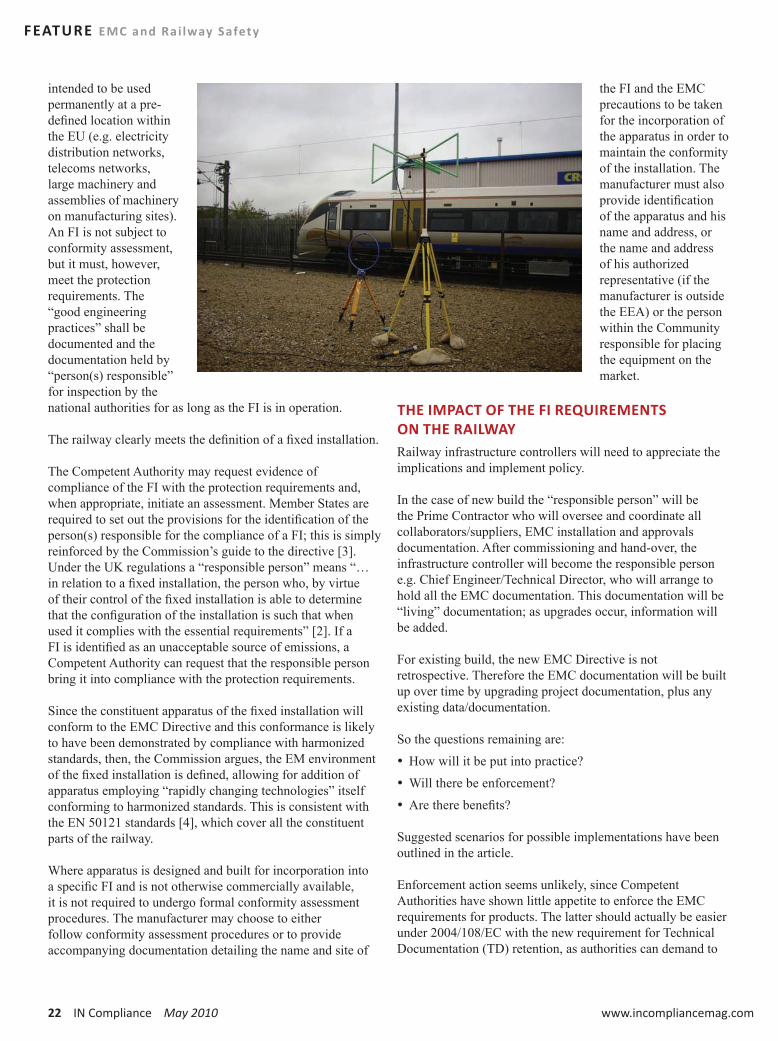
22 IN Compliance May 2010 www.incompliancemag.com
FEATURE EMC and Rai lway Safety
intended to be used permanently at a pre-defined location within the EU (e.g. electricity distribution networks, telecoms networks, large machinery and assemblies of machinery on manufacturing sites). An FI is not subject to conformity assessment, but it must, however, meet the protection requirements. The “good engineering practices” shall be documented and the documentation held by “person(s) responsible” for inspection by the national authorities for as long as the FI is in operation.
The railway clearly meets the definition of a fixed installation.
The Competent Authority may request evidence of compliance of the FI with the protection requirements and, when appropriate, initiate an assessment. Member States are required to set out the provisions for the identification of the person(s) responsible for the compliance of a FI; this is simply reinforced by the Commission’s guide to the directive [3]. Under the UK regulations a “responsible person” means “…in relation to a fixed installation, the person who, by virtue of their control of the fixed installation is able to determine that the configuration of the installation is such that when used it complies with the essential requirements” [2]. If a FI is identified as an unacceptable source of emissions, a Competent Authority can request that the responsible person bring it into compliance with the protection requirements.
Since the constituent apparatus of the fixed installation will conform to the EMC Directive and this conformance is likely to have been demonstrated by compliance with harmonized standards, then, the Commission argues, the EM environment of the fixed installation is defined, allowing for addition of apparatus employing “rapidly changing technologies” itself conforming to harmonized standards. This is consistent with the EN 50121 standards [4], which cover all the constituent parts of the railway.
Where apparatus is designed and built for incorporation into a specific FI and is not otherwise commercially available, it is not required to undergo formal conformity assessment procedures. The manufacturer may choose to either follow conformity assessment procedures or to provide accompanying documentation detailing the name and site of
the FI and the EMC precautions to be taken for the incorporation of the apparatus in order to maintain the conformity of the installation. The manufacturer must also provide identification of the apparatus and his name and address, or the name and address of his authorized representative (if the manufacturer is outside the EEA) or the person within the Community responsible for placing the equipment on the market.
THE IMPACT OF THE FI REQUIREMENTS ON THE RAILWAYRailway infrastructure controllers will need to appreciate the implications and implement policy.
In the case of new build the “responsible person” will be the Prime Contractor who will oversee and coordinate all collaborators/suppliers, EMC installation and approvals documentation. After commissioning and hand-over, the infrastructure controller will become the responsible person e.g. Chief Engineer/Technical Director, who will arrange to hold all the EMC documentation. This documentation will be “living” documentation; as upgrades occur, information will be added.
For existing build, the new EMC Directive is not retrospective. Therefore the EMC documentation will be built up over time by upgrading project documentation, plus any existing data/documentation.
So the questions remaining are:
y How will it be put into practice?
y Will there be enforcement?
y Are there benefits?
Suggested scenarios for possible implementations have been outlined in the article.
Enforcement action seems unlikely, since Competent Authorities have shown little appetite to enforce the EMC requirements for products. The latter should actually be easier under 2004/108/EC with the new requirement for Technical Documentation (TD) retention, as authorities can demand to
24 IN Compliance May 2010 www.incompliancemag.com
FEATURE EMC and Rai lway Safety
see the TD, not just a Declaration of Conformity (DoC). We shall wait with interest!
There are benefits. The FI requirements lend weight to the need for a structured approach to EMC encompassing safety aspects, interoperability and EMC Directive conformance. This model can clearly be used in non-EU countries as a means of demonstrating EMC assurance for railways.
It should be noted that the FI regulatory regime came into effect in July 2007. The FI documentation, based on recording “good engineering practices,” includes initial EM site surveys to benchmark the environment, EMC Management Plans, hazard identification, the use of compliance matrices and in many instances on-site testing to verify that the measures undertaken ensure that EMC has been achieved.
EMC MANAGEMENTIn order to achieve EMC for railway equipment it is necessary to include EMC as a design parameter from the concept stage of a project. It is also necessary to control the design process to ensure that the documentation is produced which will support and be included within the Safety Case to cover the EMC aspects of safety and which will enable the manufacturer to declare conformance with appropriate EMC regulations.
The first stage of this process is to include EMC as a requirement within the Invitation to Tender (ITT) and to include an EMC specification. At this stage it may simply define the EN 50121-x:2006 series of standards plus the appropriate infrastructure standards eg RSSB Group standards such as GM/RC 1500, GM/RT8015 or the London Underground standard 2-01018-001/1-222 A1 and manual of best practice 5-01018-001/ G-222 A1. The main contractor will then produce an EMC Management Plan (also known as an EMC Control Plan or EMC Strategy Document) which should be drawn up at the commencement of the project and typically will include: y A hazard identification (HAZID): an identification of the likely sources of interference from the equipment that will affect other equipment in the operating environment; an identification of the sources of interference in the environment affecting or likely to affect the system;
y A listing of references: for example, the appropriate EMC regulations, customer specifications, standards, or in-house specifications;
y The EMC management rationale;
y Definition of responsibilities of the prime contractor and his suppliers;
y Control of suppliers: this may include the requirement for each supplier to produce an EMC plan and to demonstrate compliance;
y “Whole system EMC management,” declaring the overall intention of managing EMC by design, identifying particular areas of concern;
y Deliverable documentation;
y EMC time management: identification of milestones e.g. on-site whole system EMC emission tests, for incorporation into whole project plan.
y Appended to the EMC Management Plan will be the EMC design guidelines and practices used by the prime contractor.
For a large system, whilst it will be necessary to perform some EMC measurements on the whole system, initially it is necessary to identify the various electrical sub-systems and
determine the procurement policy from suppliers. In this instance a reasonable approach is to task each sub-contractor with providing documentary evidence that his product is compliant with appropriate standards.
As indicated by the management plan, each supplier will be responsible for demonstrating that his equipment meets the EMC requirements specified and will submit his EMC Control Plan, Test Plans and Test Reports to the system contractor who will include these within the system
EMC Technical Documentation. It is then necessary for the system manufacturer to validate, from an EMC viewpoint, the installation and wiring techniques he has used. This will be partly by reference to the management plan, which lays down the essential EMC working practices, by reference to the Quality Assurance procedures for the contractor’s organization, but also verification, by whole-system EMC emission tests.
May 2010 IN Compliance 25
EMC and Rai lway Safety FEATURE
Immunity testing may be largely impractical on-site for large systems and reliance must be placed on the integrity of the immunity testing performed on the individual items of apparatus or systems and the installation practices used. It is vital that the installation practices must ensure that the integrity of the sub-system immunity is maintained, whether by using for example, screened cables, cable separation, or grounding and bonding techniques. Hence good communication is required between supplier and main contractor to ensure the flow of information. It should be noted that for European apparatus carrying the CE Marking it is a legal requirement to provide the user with “user information,” covering installation and operation of equipment.
A NOVEL TECHNIQUE FOR MEASURING EMISSIONS FROM HIGH SPEED TRAINSThe EN 50121-2 and EN 50121-3-1 require emissions to be measured from moving trains from a single observation point at the side of the railway. The measurements need to be made using a peak detector since the “window of opportunity” to make the measurement is very small and is derived from the beam width of the antenna, the scan rate of the measuring instrument and the speed of the train. This means that transient emissions, such as those due to pantograph bounce or shoegear gapping are included in the actual measurement.
The standard limits are derived from such measurements which mean that potentially a manufacturer of rolling stock can produce continuous emissions up to these limits and so we may have “noisier” trains than in the past! Also the standards require individual train passes for different frequency ranges, a time consuming and expensive operation, usually requiring the measurements to be made on a test track or on the network during a possession.
CONCLUSIONSFor EMC assurance for equipment or large installed systems, within the railway environment, a practical approach has been described which relies on rigorous testing of sub-systems and the verification of installation and design practices by a combination of managing EMC from the outset, QA procedures and whole system emission testing accepting practical limitations.
This approach can be seen to fulfill demonstration of the essential protection requirements of the EMC Directive, in Europe, in relation to effect of the system on the external environment, the need to control the internal EMC within the system and the manufacturer’s need to satisfy a court that he has used all due diligence to avoid committing an offence.
Further the EMC Technical Documentation and the incorporated test data can be used to support the EMC aspects of the equipment/system Safety Case and in the case of signalling projects, for example, the documentation can be added to the EMC “Fixed Installation” documentation for the railway. It must be stressed that the railway EMC standards represent the minimum technical requirement and that additional measures may need to be taken on the basis of the hazard identification and risk closure.
The technical difficulties of making EMC measurements on moving trains have been addressed and a cost effective solution referred to.
ACKNOWLEDGEMENTSThe authors gratefully acknowledge access to information held by York EMC Services Ltd, University of York. They also acknowledge the experiences gained from YES Ltd customers who have successfully prepared Technical Documentation and TCFs for conformance with the European EMC Directives and have used test data to close out the EMC issues raised in Hazard Logs.
REFERENCES1. Directive 2004/108/EC of the European Parliament
and of the Council of 15 December 2004 on the approximation of the laws of the Member States relating to electromagnetic compatibility and repealing Directive 89/336/EEC, Official Journal of the European Union (OJEU) L 390/24 dated 31.12.2004, pp24 – 36.
2. “The Electromagnetic Compatibility Regulations 2006,” Statutory Instruments 2006 No. 3418, December 2006.
3. “Guide for the EMC Directive 2004/108/EC,” EMC WG of the European Commission, 22 March 2007.
4. “Railway applications – Electromagnetic Compatibility,” EN50121-X:2006 (5 parts), CENELEC, 2006.
5. “EMC in Railways,” Course Notes, C.A.Marshman, York EMC Services Ltd.
6. “Improved Measurement of Radiated Emissions from Moving Rail Vehicles in the Frequency Range 9 kHz to 1 GHz,” AJ Rowell, D Bozec, S A Seller, L M McCormack, C A Marshman and A C Marvin, IEEE EMC Symposium 2004.
Chris Marshman is the Managing Director and Nick Wainwright the Operations Director of York EMC Services Ltd, operating three UKAS accredited EMC testing laboratories and BIS appointed Notified Body. YES Ltd provides EMC consultancy, testing and training services to the railway industry. They can be reached by phone at +44(0)1904 434440 or at [email protected].
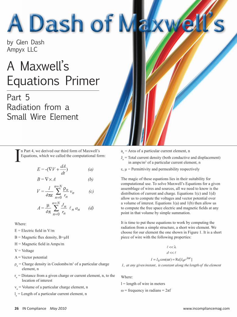
26 IN Compliance May 2010 www.incompliancemag.com
In Part 4, we derived our third form of Maxwell’s Equations, which we called the computational form:
Where:
E = Electric field in V/m
B = Magnetic flux density, B=µH
H = Magnetic field in Amps/m
V = Voltage
A = Vector potential
ρn = Charge density in Coulombs/m3 of a particular charge element, n
rn = Distance from a given charge or current element, n, to the location of interest
vn = Volume of a particular charge element, n
ln = Length of a particular current element, n
an = Area of a particular current element, n
Jn = Total current density (both conductive and displacement) in amps/m2 of a particular current element, n
ε, µ = Permittivity and permeability respectively
The magic of these equations lies in their suitability for computational use. To solve Maxwell’s Equations for a given assemblage of wires and sources, all we need to know is the distribution of current and charge. Equations 1(c) and 1(d) allow us to compute the voltages and vector potential over a volume of interest. Equations 1(a) and 1(b) then allow us to compute the free space electric and magnetic fields at any point in that volume by simple summation.
It is time to put these equations to work by computing the radiation from a simple structure, a short wire element. We choose for our element the one shown in Figure 1. It is a short piece of wire with the following properties:
Where:
l = length of wire in meters
ω = frequency in radians = 2πf
by Glen DashAmpyx LLC
A Dash of Maxwell’sA Maxwell’sEquations PrimerPart 5Radiation from a Small Wire Element
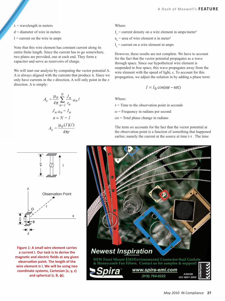
May 2010 IN Compliance 27
A Dash of Maxwel l ’s FEATURE
λ = wavelength in meters
d = diameter of wire in meters
I = current on the wire in amps
Note that this wire element has constant current along its entire finite length. Since the current has to go somewhere, two plates are provided, one at each end. They form a capacitor and serve as reservoirs of charge.
We will start our analysis by computing the vector potential A. A is always aligned with the currents that produce it. Since we only have currents in the z direction, A will only point in the z direction. A is simply:
Where:
Jn = current density on a wire element in amps/meter2
an = area of wire element n in meter2
In = current on a wire element in amps
However, these results are not complete. We have to account for the fact that the vector potential propagates as a wave through space. Since our hypothetical wire element is suspended in free space, this wave propagates away from the wire element with the speed of light, c. To account for this propagation, we adjust the solution in by adding a phase term:
Where:
τ = Time to the observation point in seconds
ω = Frequency in radians per second
ωτ = Total phase change in radians
The term ωτ accounts for the fact that the vector potential at the observation point is a function of something that happened earlier, namely the current at the source at time t-τ . The time
Figure 1: A small wire element carries a current I. Our task is to derive the
magnetic and electric fields at any given observation point. The length of the
wire element is l. We will be using two coordinate systems, Cartesian (x, y, z)
and spherical (r, θ, φ).
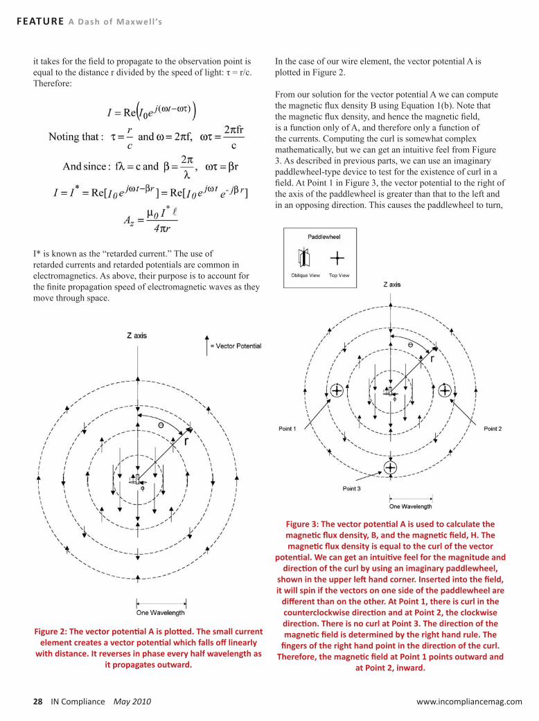
28 IN Compliance May 2010 www.incompliancemag.com
FEATURE A Dash of Maxwel l ’s
it takes for the field to propagate to the observation point is equal to the distance r divided by the speed of light: τ = r/c. Therefore:
I* is known as the “retarded current.” The use of retarded currents and retarded potentials are common in electromagnetics. As above, their purpose is to account for the finite propagation speed of electromagnetic waves as they move through space.
In the case of our wire element, the vector potential A is plotted in Figure 2.
From our solution for the vector potential A we can compute the magnetic flux density B using Equation 1(b). Note that the magnetic flux density, and hence the magnetic field, is a function only of A, and therefore only a function of the currents. Computing the curl is somewhat complex mathematically, but we can get an intuitive feel from Figure 3. As described in previous parts, we can use an imaginary paddlewheel-type device to test for the existence of curl in a field. At Point 1 in Figure 3, the vector potential to the right of the axis of the paddlewheel is greater than that to the left and in an opposing direction. This causes the paddlewheel to turn,
Figure 2: The vector potential A is plotted. The small current element creates a vector potential which falls off linearly
with distance. It reverses in phase every half wavelength as it propagates outward.
Figure 3: The vector potential A is used to calculate the magnetic flux density, B, and the magnetic field, H. The magnetic flux density is equal to the curl of the vector
potential. We can get an intuitive feel for the magnitude and direction of the curl by using an imaginary paddlewheel,
shown in the upper left hand corner. Inserted into the field, it will spin if the vectors on one side of the paddlewheel are
different than on the other. At Point 1, there is curl in the counterclockwise direction and at Point 2, the clockwise direction. There is no curl at Point 3. The direction of the magnetic field is determined by the right hand rule. The
fingers of the right hand point in the direction of the curl. Therefore, the magnetic field at Point 1 points outward and
at Point 2, inward.
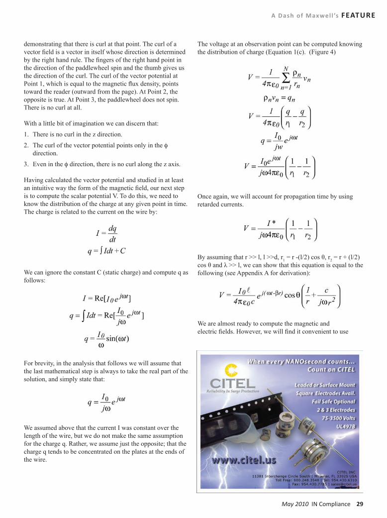
May 2010 IN Compliance 29
A Dash of Maxwel l ’s FEATURE
demonstrating that there is curl at that point. The curl of a vector field is a vector in itself whose direction is determined by the right hand rule. The fingers of the right hand point in the direction of the paddlewheel spin and the thumb gives us the direction of the curl. The curl of the vector potential at Point 1, which is equal to the magnetic flux density, points toward the reader (outward from the page). At Point 2, the opposite is true. At Point 3, the paddlewheel does not spin. There is no curl at all.
With a little bit of imagination we can discern that:
1. There is no curl in the z direction.
2. The curl of the vector potential points only in the φ direction.
3. Even in the φ direction, there is no curl along the z axis.
Having calculated the vector potential and studied in at least an intuitive way the form of the magnetic field, our next step is to compute the scalar potential V. To do this, we need to know the distribution of the charge at any given point in time. The charge is related to the current on the wire by:
We can ignore the constant C (static charge) and compute q as follows:
For brevity, in the analysis that follows we will assume that the last mathematical step is always to take the real part of the solution, and simply state that:
We assumed above that the current I was constant over the length of the wire, but we do not make the same assumption for the charge q. Rather, we assume just the opposite; that the charge q tends to be concentrated on the plates at the ends of the wire.
The voltage at an observation point can be computed knowing the distribution of charge (Equation 1(c). (Figure 4)
Once again, we will account for propagation time by using retarded currents.
By assuming that r >> l, l >>d, r1 = r -(l/2) cos θ, r2 = r + (l/2) cos θ and λ >> l, we can show that this equation is equal to the following (see Appendix A for derivation):
We are almost ready to compute the magnetic and electric fields. However, we will find it convenient to use
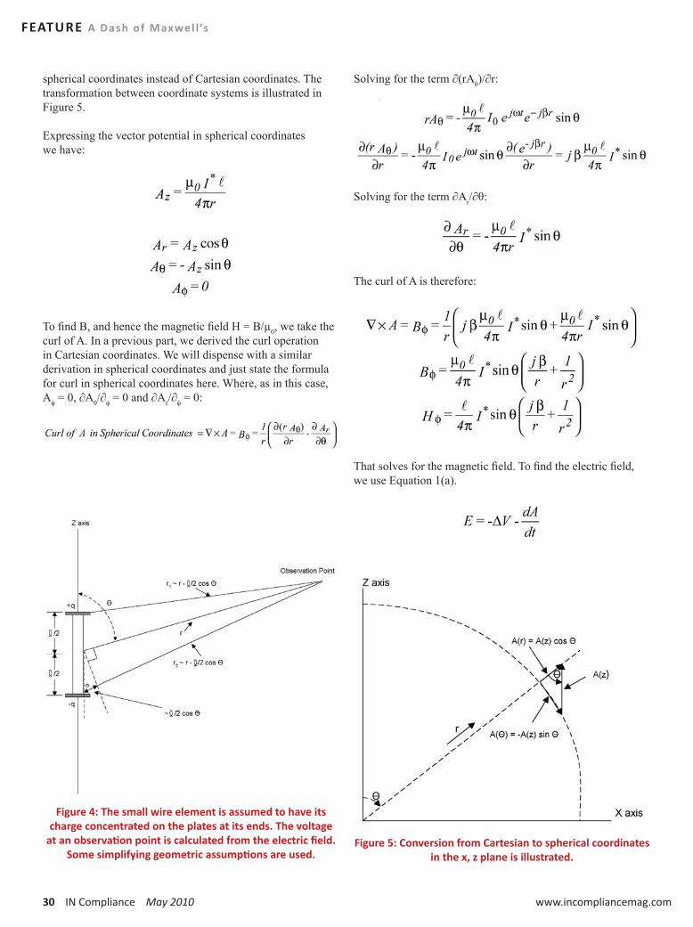
30 IN Compliance May 2010 www.incompliancemag.com
FEATURE A Dash of Maxwel l ’s
spherical coordinates instead of Cartesian coordinates. The transformation between coordinate systems is illustrated in Figure 5.
Expressing the vector potential in spherical coordinates we have:
To find B, and hence the magnetic field H = B/µ0, we take the curl of A. In a previous part, we derived the curl operation in Cartesian coordinates. We will dispense with a similar derivation in spherical coordinates and just state the formula for curl in spherical coordinates here. Where, as in this case, A
φ = 0, ∂Aθ/∂φ
= 0 and ∂Ar/∂φ = 0:
Solving for the term ∂(rAθ)/∂r:
Solving for the term ∂Ar/∂θ:
The curl of A is therefore:
That solves for the magnetic field. To find the electric field, we use Equation 1(a).
Figure 4: The small wire element is assumed to have its charge concentrated on the plates at its ends. The voltage
at an observation point is calculated from the electric field. Some simplifying geometric assumptions are used.
Figure 5: Conversion from Cartesian to spherical coordinates in the x, z plane is illustrated.
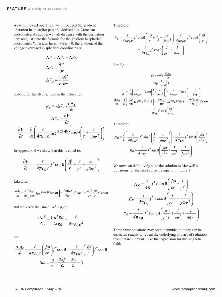
32 IN Compliance May 2010 www.incompliancemag.com
FEATURE A Dash of Maxwel l ’s
As with the curl operation, we introduced the gradient operation in an earlier part and derived it in Cartesian coordinates. As above, we will dispense with the derivation here and just state the formula for the gradient in spherical coordinates. Where, as here, ∂V/∂φ = 0, the gradient of the voltage expressed in spherical coordinates is:
Solving for the electric field in the r direction:
In Appendix B we show that this is equal to:
Likewise:
But we know that since 1/c2 = µ0ε0:
So:
Therefore:
For Eθ:
Therefore:
We now can definitively state the solution to Maxwell’s Equations for the short current element in Figure 1:
These three equations may seem a jumble, but they can be dissected readily to reveal the underlying physics of radiation from a wire element. Take the expression for the magnetic field:
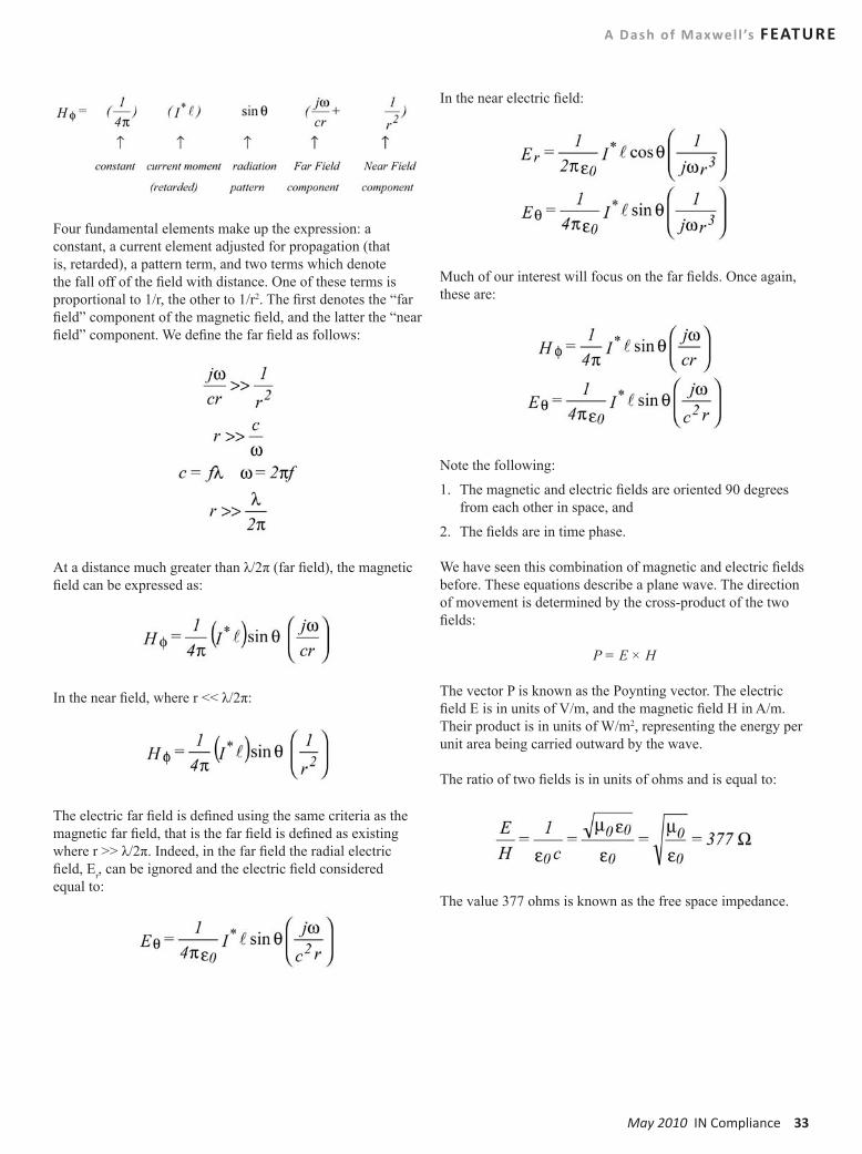
May 2010 IN Compliance 33
A Dash of Maxwel l ’s FEATURE
Four fundamental elements make up the expression: a constant, a current element adjusted for propagation (that is, retarded), a pattern term, and two terms which denote the fall off of the field with distance. One of these terms is proportional to 1/r, the other to 1/r2. The first denotes the “far field” component of the magnetic field, and the latter the “near field” component. We define the far field as follows:
At a distance much greater than λ/2π (far field), the magnetic field can be expressed as:
In the near field, where r << λ/2π:
The electric far field is defined using the same criteria as the magnetic far field, that is the far field is defined as existing where r >> λ/2π. Indeed, in the far field the radial electric field, Er, can be ignored and the electric field considered equal to:
In the near electric field:
Much of our interest will focus on the far fields. Once again, these are:
Note the following:
1. The magnetic and electric fields are oriented 90 degrees from each other in space, and
2. The fields are in time phase.
We have seen this combination of magnetic and electric fields before. These equations describe a plane wave. The direction of movement is determined by the cross-product of the two fields:
P = E × H
The vector P is known as the Poynting vector. The electric field E is in units of V/m, and the magnetic field H in A/m. Their product is in units of W/m2, representing the energy per unit area being carried outward by the wave.
The ratio of two fields is in units of ohms and is equal to:
The value 377 ohms is known as the free space impedance.
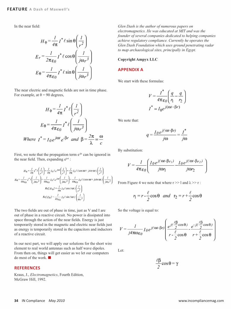
34 IN Compliance May 2010 www.incompliancemag.com
FEATURE A Dash of Maxwel l ’s
In the near field:
The near electric and magnetic fields are not in time phase. For example, at θ = 90 degrees,
First, we note that the propagation term e-βr can be ignored in the near field. Then, expanding ejωt :
The two fields are out of phase in time, just as V and I are out of phase in a reactive circuit. No power is dissipated into space through the action of the near fields. Energy is just temporarily stored in the magnetic and electric near fields just as energy is temporarily stored in the capacitors and inductors of a reactive circuit.
In our next part, we will apply our solutions for the short wire element to real world antennas such as half wave dipoles. From then on, things will get easier as we let our computers do most of the work. n
REFERENCESKraus, J., Electromagnetics, Fourth Edition, McGraw Hill, 1992.
Glen Dash is the author of numerous papers on electromagnetics. He was educated at MIT and was the founder of several companies dedicated to helping companies achieve regulatory compliance. Currently he operates the Glen Dash Foundation which uses ground penetrating radar to map archaeological sites, principally in Egypt.
Copyright Ampyx LLC
APPENDIX A
We start with these formulas:
We note that:
By substitution:
From Figure 4 we note that where r >> l and λ >> r :
So the voltage is equal to:
Let:
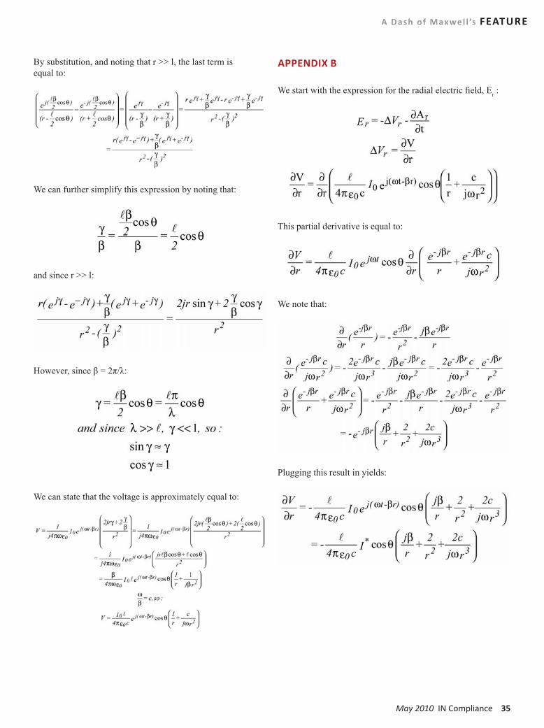
May 2010 IN Compliance 35
A Dash of Maxwel l ’s FEATURE
By substitution, and noting that r >> l, the last term is equal to:
We can further simplify this expression by noting that:
and since r >> l:
However, since β = 2π/λ:
We can state that the voltage is approximately equal to:
APPENDIX B
We start with the expression for the radial electric field, Er :
This partial derivative is equal to:
We note that:
Plugging this result in yields:
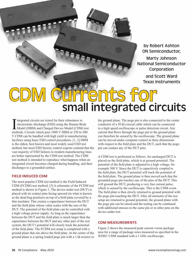
36 IN Compliance May 2010 www.incompliancemag.com
Integrated circuits are tested for their robustness to electrostatic discharge (ESD) using the Human Body Model (HBM) and Charged Device Model (CDM) test
methods. Circuits which pass 1000 V HBM or 250 to 500 V CDM can be handled with high yield in manufacturing facilities using basic ESD control procedures. [1, 2] HBM is the oldest, best known and most widely used ESD test method, but most ESD factory control experts contend that the vast majority of ESD failures in modern manufacturing lines are better represented by the CDM test method. The CDM test method is intended to reproduce what happens when an integrated circuit becomes charged during handling, and then discharges to a grounded surface.
FIELD INDUCED CDMThe most popular CDM test method is the Field Induced CDM (FCDM) test method. [3] A schematic of the FCDM test method is shown in Figure 1. The device under test (DUT) is placed with its contact pins facing upward (in what is known as the dead bug position) on top of a field plate covered by a thin insulator. This creates a capacitance between the DUT and the field plate whose value scales with the size of the DUT. The potential of the field plate can be controlled with a high voltage power supply. As long as the capacitance between the DUT and the field plate is much larger than the capacitance between the DUT and any other part of the test system, the DUT’s potential will closely track the potential of the field plate. The FCDM test setup is completed with a ground plane that sits above the field plate. At the center of the ground plane is a spring loaded pogo pin with a 1 Ω resistor to
the ground plane. The pogo pin is also connected to the center conductor of a 50 Ω coaxial cable which can be connected to a high speed oscilloscope or pulse detection circuit. Any current that flows through the pogo pin to the ground plane can therefore be sensed by the oscilloscope. The ground plane can be moved under computer control in three dimensions with respect to the field plate and the DUT, such that the pogo pin can contact any of the DUT pins.
A CDM test is performed as follows. An uncharged DUT is placed on the field plate, which is at ground potential. The potential of the field plate is adjusted to a high voltage, for example 500 V. Since the DUT is capacitively coupled to the field plate, the DUT potential will track the potential of the field plate. The ground plane is then moved such that the grounded pogo pin touches one of the pins of the DUT. This will ground the DUT, producing a very fast current pulse, which is sensed by the oscilloscope. This is the CDM event. The field plate is then slowly returned to ground potential with the pogo pin touching the DUT. After all elements of the test setup are returned to ground potential, the ground plane with the pogo pin can be raised and the testing can be continued with additional stresses to the same pin or to other pins on the device under test.
CDM MEASUREMENTSFigure 2 shows the measured peak current versus package area for a range of package sizes measured as specified in the JEDEC CDM standard with a 1 GHz oscilloscope.
by Robert Ashton ON Semiconductor,
Marty Johnson National Semiconductor
Corporationand Scott Ward
Texas Instruments
CDM Currents for small integrated circuits
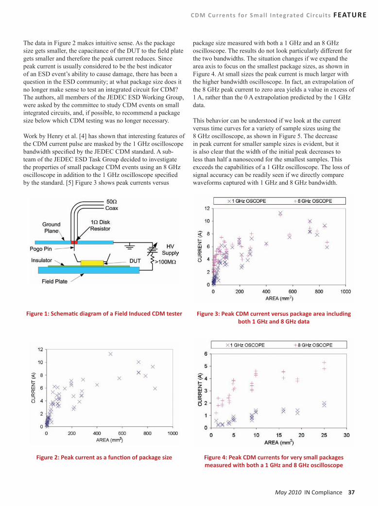
May 2010 IN Compliance 37
CDM Currents for Smal l Integrated Circuits FEATURE
The data in Figure 2 makes intuitive sense. As the package size gets smaller, the capacitance of the DUT to the field plate gets smaller and therefore the peak current reduces. Since peak current is usually considered to be the best indicator of an ESD event’s ability to cause damage, there has been a question in the ESD community; at what package size does it no longer make sense to test an integrated circuit for CDM? The authors, all members of the JEDEC ESD Working Group, were asked by the committee to study CDM events on small integrated circuits, and, if possible, to recommend a package size below which CDM testing was no longer necessary.
Work by Henry et al. [4] has shown that interesting features of the CDM current pulse are masked by the 1 GHz oscilloscope bandwidth specified by the JEDEC CDM standard. A sub-team of the JEDEC ESD Task Group decided to investigate the properties of small package CDM events using an 8 GHz oscilloscope in addition to the 1 GHz oscilloscope specified by the standard. [5] Figure 3 shows peak currents versus
package size measured with both a 1 GHz and an 8 GHz oscilloscope. The results do not look particularly different for the two bandwidths. The situation changes if we expand the area axis to focus on the smallest package sizes, as shown in Figure 4. At small sizes the peak current is much larger with the higher bandwidth oscilloscope. In fact, an extrapolation of the 8 GHz peak current to zero area yields a value in excess of 1 A, rather than the 0 A extrapolation predicted by the 1 GHz data.
This behavior can be understood if we look at the current versus time curves for a variety of sample sizes using the 8 GHz oscilloscope, as shown in Figure 5. The decrease in peak current for smaller sample sizes is evident, but it is also clear that the width of the initial peak decreases to less than half a nanosecond for the smallest samples. This exceeds the capabilities of a 1 GHz oscilloscope. The loss of signal accuracy can be readily seen if we directly compare waveforms captured with 1 GHz and 8 GHz bandwidth.
Figure 1: Schematic diagram of a Field Induced CDM tester
Figure 2: Peak current as a function of package size
Figure 3: Peak CDM current versus package area including both 1 GHz and 8 GHz data
Figure 4: Peak CDM currents for very small packages measured with both a 1 GHz and 8 GHz oscilloscope
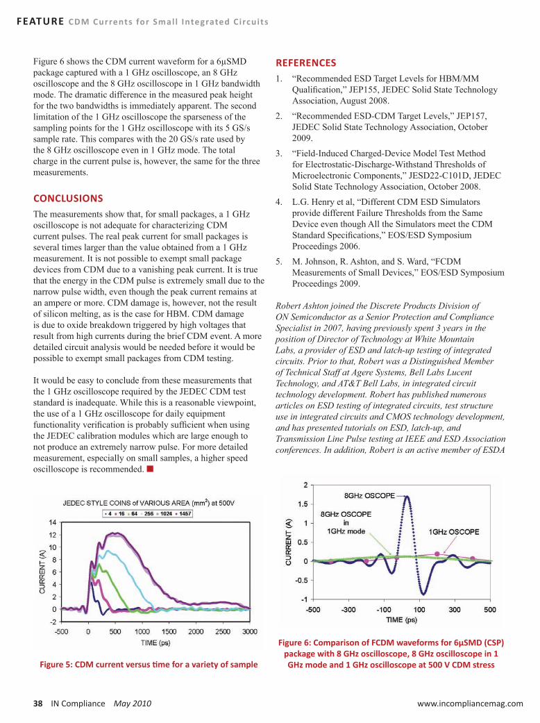
38 IN Compliance May 2010 www.incompliancemag.com
FEATURE CDM Currents for Smal l Integrated Circuits
Figure 6 shows the CDM current waveform for a 6µSMD package captured with a 1 GHz oscilloscope, an 8 GHz oscilloscope and the 8 GHz oscilloscope in 1 GHz bandwidth mode. The dramatic difference in the measured peak height for the two bandwidths is immediately apparent. The second limitation of the 1 GHz oscilloscope the sparseness of the sampling points for the 1 GHz oscilloscope with its 5 GS/s sample rate. This compares with the 20 GS/s rate used by the 8 GHz oscilloscope even in 1 GHz mode. The total charge in the current pulse is, however, the same for the three measurements.
CONCLUSIONSThe measurements show that, for small packages, a 1 GHz oscilloscope is not adequate for characterizing CDM current pulses. The real peak current for small packages is several times larger than the value obtained from a 1 GHz measurement. It is not possible to exempt small package devices from CDM due to a vanishing peak current. It is true that the energy in the CDM pulse is extremely small due to the narrow pulse width, even though the peak current remains at an ampere or more. CDM damage is, however, not the result of silicon melting, as is the case for HBM. CDM damage is due to oxide breakdown triggered by high voltages that result from high currents during the brief CDM event. A more detailed circuit analysis would be needed before it would be possible to exempt small packages from CDM testing.
It would be easy to conclude from these measurements that the 1 GHz oscilloscope required by the JEDEC CDM test standard is inadequate. While this is a reasonable viewpoint, the use of a 1 GHz oscilloscope for daily equipment functionality verification is probably sufficient when using the JEDEC calibration modules which are large enough to not produce an extremely narrow pulse. For more detailed measurement, especially on small samples, a higher speed oscilloscope is recommended. n
REFERENCES1. “Recommended ESD Target Levels for HBM/MM
Qualification,” JEP155, JEDEC Solid State Technology Association, August 2008.
2. “Recommended ESD-CDM Target Levels,” JEP157, JEDEC Solid State Technology Association, October 2009.
3. “Field-Induced Charged-Device Model Test Method for Electrostatic-Discharge-Withstand Thresholds of Microelectronic Components,” JESD22-C101D, JEDEC Solid State Technology Association, October 2008.
4. L.G. Henry et al, “Different CDM ESD Simulators provide different Failure Thresholds from the Same Device even though All the Simulators meet the CDM Standard Specifications,” EOS/ESD Symposium Proceedings 2006.
5. M. Johnson, R. Ashton, and S. Ward, “FCDM Measurements of Small Devices,” EOS/ESD Symposium Proceedings 2009.
Robert Ashton joined the Discrete Products Division of ON Semiconductor as a Senior Protection and Compliance Specialist in 2007, having previously spent 3 years in the position of Director of Technology at White Mountain Labs, a provider of ESD and latch-up testing of integrated circuits. Prior to that, Robert was a Distinguished Member of Technical Staff at Agere Systems, Bell Labs Lucent Technology, and AT&T Bell Labs, in integrated circuit technology development. Robert has published numerous articles on ESD testing of integrated circuits, test structure use in integrated circuits and CMOS technology development, and has presented tutorials on ESD, latch-up, and Transmission Line Pulse testing at IEEE and ESD Association conferences. In addition, Robert is an active member of ESDA
Figure 5: CDM current versus time for a variety of sample
Figure 6: Comparison of FCDM waveforms for 6µSMD (CSP) package with 8 GHz oscilloscope, 8 GHz oscilloscope in 1 GHz mode and 1 GHz oscilloscope at 500 V CDM stress
May 2010 IN Compliance 39
CDM Currents for Smal l Integrated Circuits FEATURE
Working Group 5 for Device Standards, ESDA Working Group 14 for System Level Test as well as the JEDEC Committee 14.1 ESD and Latch-Up Working Groups and the IEEE Surge Protection Device Committee.
Robert received his B.S. and Ph.D. in Physics from the University of Rhode Island in Kinston, RI, USA in 1971 and 1977.
Marty Johnson returned to National Semiconductor in 2006 working in ESD device design debug and supervising the ESD Characterization Lab. He currently is supervisor of the ESD Qualification & Characterization Lab. From 2001 to 2006, he worked at Philips Electronics (Semiconductor Division) focusing on WLR and TLP characterization. During his tenure at Philips he was the corporate representative to the Reliability Technology Advisory Board (RTAB, now ISMI) and its chairman in 2004. From 1978 to 2001, he worked for National Semiconductor spanning the semiconductor reliability spectrum from basic reliability qualification through wafer level reliability to ESD and Latch-up. He is also active on the JEDEC ESD Team (JC-14.1), the Joint ESDA/JEDEC HBM and CDM teams and the JEDEC Latch-up Standards team.
Marty received his B.S. Physics from Midland Lutheran College in 1973, his M.S. Physics from the University of Tennessee Space Institute in 1975 and his M.S. in Electrical Engineering from the University of Nebraska in 1978.
Scott Ward joined Texas Instruments in 2007 to work in the field of device-level ESD testing and ESD testing standards development. He has since expanded his work to include factory ESD control and handling. Prior to Texas Instruments, Scott worked for Cypress Semiconductor in San Jose, CA. At Cypress, his work included ESD and Latch-up design and characterization; as well as device testing standards development. Since 2003, he has been a member of the ESDA Working Group 5 standards committee (device testing). Scott joined the JEDEC ESD standards task force in 2005. Scott is an ESDA member, attending every EOS/ESD Symposium since his first in 1996. Scott began his career at ZiLOG in 1995, designing on-chip ESD protection networks.
Scott has an M.S. in Electrical Engineering from the University of Idaho and a B.S. in Electrical Engineering from Montana State University.
White Papersavailable for download from www.incompliancemag.com
What is Functional Safety?
Key Steps to Rapid Global PV Module Certification
EMC for Active Implantable Medical Devices
Insider’s Guide to Faster Safety & EMC Testing
The Five Key Factors Driving RoHS Compliance of Medical Electronics
Streamline: Progressions in Product Compliance
by Terry WelsherSenior Vice President, Dangelmayer Associates and Vice President, ESD Association
The “Real” Cost of ESD Damage
May 2010 IN Compliance 41
The “Real” Cost of ESD Damage FEATURE
Anyone who has worked in Quality or Reliability in a large corporation knows that developing and presenting credible failure cost information can
be difficult. This is particularly true for ESD, where the events are invisible and not nearly as well understood as other more obvious classes of failure, such as mechanical or contamination. The “real” cost of ESD can be a hot topic of discussion each year when program budgets are being developed for manufacturing and R&D programs. The challenge is that every year there are new high-level people in the financial and planning organizations who are not technical experts and who are asking hard questions about the justification for the ESD investment. In years when revenue is down, the questions become more difficult and better evidence is often demanded. The author was directly involved in this process for 15 years, starting in 1986. At the time the following quote was a part of many ESD funding discussions; “… in the electronics industry, losses associated with ESD are estimated at between a half billion and five billion dollars annually.” The exact original reference for this assertion has been lost, at least to this author. Nonetheless it was used many times over the next few years in presentations to the corporate check writers. Furthermore, during research for background information for this article, the exact same quote appeared (unattributed) in an article from 1992 [1] and in a book published in 2006 [2]. Needless to say, a well-stated assertion of value can go a long way – at least in trade literature. However, this author can also report that the usefulness of this, inside the corporation, eroded much faster. By 1990, a well-known director in Bell Labs said; “… that was then… I think this problem has been solved!” Many of us would scoff at such a declaration, knowing full well that ESD problems were continuing to occur. However, the directors’ challenge was an appropriate one. His experience came from the semiconductor process world where he had seen significant ESD sources eliminated and device thresholds (albeit HBM only) steadily increase. Corporations would like their investments to be justified by more timely and relevant data and observations. They ask, “What is the “real” cost?”
Of course the immediate “real” cost information is very difficult to determine. In fact the use of the term “real” in the title reflects the collective skepticism ESD program managers and champions typically encounter. The $5 billion dollar loss number which applies to everyone, but not to one’s own situation, carries little weight in the final analysis. As a result it is necessary to resist the temptation here to assert an updated number for world-wide losses due to ESD. Instead, this article revisits the collective argument that ESD losses are potentially significant and that pressures that produced high failure rates (based on evidence published in the past) will increase with technology trends. Further, the current cost is probably not the most significant metric. This is true of most quality, reliability or maintainability metrics. The entire justification for the investment (which is typically viewed as
expense by the financial organization) is really cost avoidance. Later in the article there will also be an argument that there are other, possibly even more important reasons for investing in ESD control and design. Making convincing arguments about potential losses have historically been very difficult as they must depend on studies done off-line or in the early days of implementation. In this article, some of the important studies and articles that have appeared over the last 30 years regarding cost/benefits are reviewed. These include some classic split lot experiments that showed the immediate impact of implementing an ESD program where none previously existed. In other more recent studies, the investigators did not have the luxury of turning their program on and off, but nonetheless they were able to extract good information for the overall value proposition. There is no claim made here that this is a comprehensive collection of the most significant work. Rather, it represents studies that are known to this author and many colleagues and which are available as public information. There were many other proprietary internal studies which established the economic justification of programs that cannot be described here.
In 1989 the ESD Association published a collection of papers [3] from the first ten years of the EOS/ESD Symposium. This collection, An ESD Management Focus, was intended to provide ESD program advocates with a single source of significant work in supporting ESD programs and highlighting management issues. To this day it is still a useful source of information as 7 of the 19 articles in the collection directly address cost and benefits of the programs. Several of the studies are summarized here.
EARLY “SPLIT -LOT” EXPERIMENTSAt the time of the first EOS/ESD symposium in 1979 there were few mature ESD programs, but many companies were trying to establish them. Some of these companies were also developing their case for management through actual split-lot experiments.
Western Electric Denver Works (1981) [4] - In this study the initial deployment of a basic ESD program was observed with careful collection of yield loss data for five key operations. Documented yield improvement up to 10.73% was observed, and with the assistance of the plant financial organization, the return-on-investment was estimated to be in the range of 900-2300%, depending on assumptions. This study was also significant in that it demonstrated that an effective program could be implemented in a very dry environment such as Denver, Colorado’s without humidity control.
Western Electric North Andover Works (1983) [5] - This work included three separate definitive experiments on the effectiveness of ESD programs. Again, since ESD controls of any kind had not yet been implemented, simple split -lot experiments could be conducted. In these experiments as
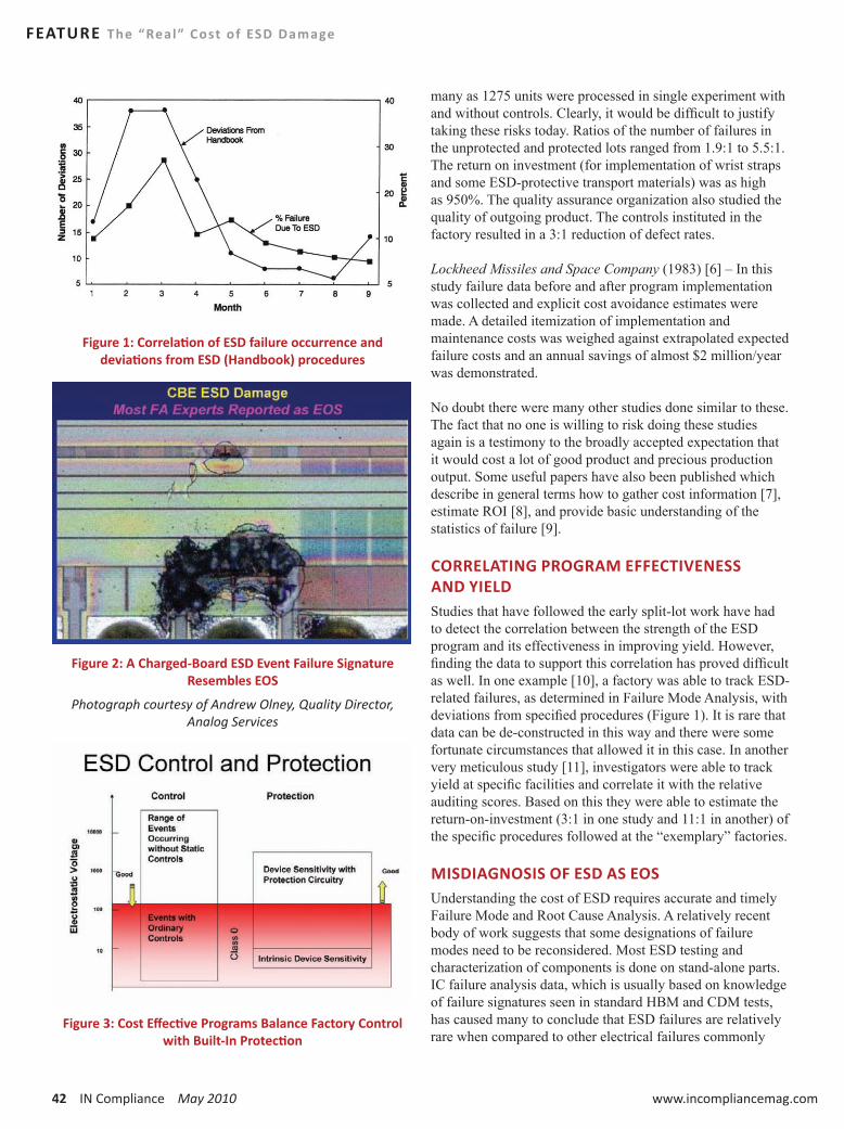
42 IN Compliance May 2010 www.incompliancemag.com
FEATURE The “Real” Cost of ESD Damage
many as 1275 units were processed in single experiment with and without controls. Clearly, it would be difficult to justify taking these risks today. Ratios of the number of failures in the unprotected and protected lots ranged from 1.9:1 to 5.5:1. The return on investment (for implementation of wrist straps and some ESD-protective transport materials) was as high as 950%. The quality assurance organization also studied the quality of outgoing product. The controls instituted in the factory resulted in a 3:1 reduction of defect rates.
Lockheed Missiles and Space Company (1983) [6] – In this study failure data before and after program implementation was collected and explicit cost avoidance estimates were made. A detailed itemization of implementation and maintenance costs was weighed against extrapolated expected failure costs and an annual savings of almost $2 million/year was demonstrated.
No doubt there were many other studies done similar to these. The fact that no one is willing to risk doing these studies again is a testimony to the broadly accepted expectation that it would cost a lot of good product and precious production output. Some useful papers have also been published which describe in general terms how to gather cost information [7], estimate ROI [8], and provide basic understanding of the statistics of failure [9].
CORRELATING PROGRAM EFFECTIVENESS AND YIELDStudies that have followed the early split-lot work have had to detect the correlation between the strength of the ESD program and its effectiveness in improving yield. However, finding the data to support this correlation has proved difficult as well. In one example [10], a factory was able to track ESD-related failures, as determined in Failure Mode Analysis, with deviations from specified procedures (Figure 1). It is rare that data can be de-constructed in this way and there were some fortunate circumstances that allowed it in this case. In another very meticulous study [11], investigators were able to track yield at specific facilities and correlate it with the relative auditing scores. Based on this they were able to estimate the return-on-investment (3:1 in one study and 11:1 in another) of the specific procedures followed at the “exemplary” factories.
MISDIAGNOSIS OF ESD AS EOSUnderstanding the cost of ESD requires accurate and timely Failure Mode and Root Cause Analysis. A relatively recent body of work suggests that some designations of failure modes need to be reconsidered. Most ESD testing and characterization of components is done on stand-alone parts. IC failure analysis data, which is usually based on knowledge of failure signatures seen in standard HBM and CDM tests, has caused many to conclude that ESD failures are relatively rare when compared to other electrical failures commonly
Figure 1: Correlation of ESD failure occurrence and deviations from ESD (Handbook) procedures
Figure 2: A Charged-Board ESD Event Failure Signature Resembles EOS
Photograph courtesy of Andrew Olney, Quality Director, Analog Services
Figure 3: Cost Effective Programs Balance Factory Control with Built-In Protection
May 2010 IN Compliance 43
The “Real” Cost of ESD Damage FEATURE
classified as electrical overstress (EOS). Recent data and experience reported by several companies and laboratories now suggest that many failures previously classified as EOS may instead be the result of ESD failures due to Charged Board Events (CBE). [12] The reason for this is that boards may store considerably more charge than is stored in the standard CDM tests. The resulting failure signature shows more physical damage (Figure 2) than a stand-alone device failure would and thus FA experts unfamiliar with this phenomenon often make the wrong diagnosis. In addition, similar observations have been made regarding the misdiagnosis of Cable Discharge Events (CDE) as EOS. [13] Some companies have estimated that about 50% of failures originally designated as EOS were actually CBE or CDE.
THE REAL “REAL” COST OF ESD – THE CRISISThe studies described above and many others like them have served the advocacy of ESD program implementation well. While they are each very specific, it is easy to argue that the effects are general. They are also posed and conducted in terms that fit well with conventional financial metrics. However, the greatest costs due to ESD have come from a different source. Each of us who has been working in this area very long knows that the most obvious example of ESD cost is the “crisis.” When viewed this way, an ESD program is more like insurance to shield the organization from disaster.
Many of these crises have become the source of symposium papers and case histories. It could be argued that even if the ROI estimates from the studies above showed that the ROI was 1:1 or even a little less, most companies would still need good ESD programs. Crises affect a different set of metrics: productivity, time-to-market, time-to-profit, timely delivery and, of course, customer perception and confidence. This is why composite failure data is so misleading. A 1% of cost of sales failure level for ESD across the industry does not reflect the fact that perhaps 0.01% led to unacceptable damage to these other metrics. Some organizations go through cycles of crisis and cost reduction, particularly when there are management changes and a lack of long term data reporting.
EFFECT OF DEVICE THRESHOLDS – CONTROL/PROTECTION BALANCEMitigation of ESD damage in electronics manufacturing depends on a dual strategy. In this discussion the focus has been on the ESD control program. However, these programs would not be nearly as effective in maintaining high yield manufacturing if it were not for the parallel efforts of device designers to provide built-in ESD protection. This situation is illustrated in Figure 3. The front line in keeping yields high is at the point where devices become so sensitive that the “usual” procedures are not sufficiently effective. Of course experts are not in complete agreement as to where this point is
44 IN Compliance May 2010 www.incompliancemag.com
FEATURE The “Real” Cost of ESD Damage
and what additional controls are necessary. The point is that the risk of increased damage and higher costs will accelerate quickly as this regime is approached. The industry as a whole has arrived at a balance between these efforts, which are primarily driven by costs involved in the two parallel approaches and which is weighed against the performance and function the customers are demanding, while of course maintaining a reasonable or decreasing product cost.
For several years this balance was tipped in favor of high device thresholds because the technology allowed it. Specifically, there had been a de facto standard of 2000 volts for the Human Body Model (HBM) ESD thresholds of integrated circuits. Recently an industry group, the Industry Council on ESD Targets, has issued two white papers addressing this issue for both HBM [14] and the Charged-Device Model (CDM) [15]. These studies have demonstrated that the de facto targets, especially the HBM level, amount to substantially increased cost with little benefit. The increased cost of maintaining these targets in increasingly dense IC technologies results in very poor ROI. The studies on CDM, whose target was less widely used at about 500 volts, further suggest that improved implementation of CDM controls will be required. This is because the CDM targets for future technology nodes will be at 250 volts and, for some high performance devices, 125 volts.
CONCLUSIONIn this article an attempt is made to bring the ESD value proposition up to date. The significant experiments done in the early development programs are relevant to today’s processes. On-going yield losses have been estimated and the operational ROI has been demonstrated many times to be significant. This alone suggests the investment in ESD control programs is a sound practice. The most significant effects, however, are the avoidance of crises, process excursions, downstream effects on higher value-added products and maintaining positive customer perception. Technology trends suggest that the value of ESD control programs will increase and that more attention will be needed to maintain and improve them.
REFERENCES1. Sandia Science News, February 1992.
2. T. Trost, “Electrostatic discharge (ESD) - Facts and faults - A review,” A 1995 article in Packaging Technology and Science, Volume 8, Issue 5, pp. 231 – 247 published on-line in 2006. (Wiley).
3. “An ESD Management Focus,” 1989 EOS/ESD Association.
4. “The Economic Benefits of an Effective Electrostatic Discharge Awareness and Control Program – An Empirical Analysis,” W. Y. McFarland, EOS-3, pp. 28-33, 1981.
5. “ESD – How Often Does It happen?” G. T. Dangelmayer, EOS-5, pp. 1-5, 1983.
6. “ESD Control Implementation and Cost Avoidance Analysis,” M. H. Downing, EOS-5, pp. 6-11, 1983.
7. “Estimating ESD Losses in the Complex Organization,” S. A. Halperin, EOS-8, pp. 12-18, 1986.
8. “ESD Control and ROI,” R. C. Allen, Evaluation Engineering, November 1999.
9. “Cost Benefit Analysis – How Much Is Enough,” R. Y. Moss, EOS/ESD Technology Europe, Spring 1990. Also available at http://www.esdjournal.com/techpapr/eosesd/analysis/enough.htm.
10. G. T. Dangelmayer, ESD Program Management, 2nd Edition, p 58, 1999.
11. “ESD Protection Measures Return on Investment Calculation and Case Study,” K. Helling, EOS-18, pp. 130-144, 1996.
12. “Real-World Printed Circuit Board Failures,” A. Olney, B. Gifford, J. Guravage, A. Righter, EOS/ESD Symposium Proceedings, EOS-25, pp. 34-43, 2003.
13. “EOS versus ESD Misdiagnosis: Charged-Board Events Are a Growing Industry Concern,” G. T. Dangelmayer, T. L. Welsher, and A. Olney, Medical Electronics Manufacturing, Spring 2009.
14. ESD Industry Council White Paper I: A Case for Lowering Component Level HBM/MM ESD Specifications and Requirements.
15. Industry Council White Paper II: A Case for Lowering Component Level CDM ESD Specifications and Requirements.
Dr. Terry L. Welsher is currently Senior Vice President of Dangelmayer Associates. He began his career in Bell Labs in 1978, where he worked on electrolytic corrosion failure mechanisms in electrical interconnection materials. In 1986 he began directing Bell Laboratories’ core expertise in electrostatic discharge (ESD). The newly formed group proceeded to produce a string of ground-breaking contributions to the field and played a key role in advancing industry standards. At his retirement from Lucent Bell Labs in 2001, he was Director of the Quality, Reliability and Test Center of Excellence. Dr. Welsher has served as Chairman of the ESDA Standards Committee and Technical Program and General Chair of the EOS/ESD Symposium. He is currently a member of the ESDA Board of Directors, and is serving as the 2010 Vice President of the ESDA. He has also been active in the JEDEC Quality and Reliability Committee and Board of Directors. Most recently he has co-led the effort to harmonize and merge JEDEC and ESDA device testing standards. He holds a B.S. in Chemistry from Florida State University and a Ph.D. in Chemical Physics from the University of Texas at Austin. Terry and his wife, Karyl, live in Suwanee, Georgia.
May 2010 IN Compliance 45
NEW PRODUCTS
New Input/Output Box for EUT Monitoring
Teseq Inc. has introduced the new IOB 4000 (Input/Output Box) for EUT (equipment under test) monitoring during EMC immunity testing. The EUT monitoring capabilities of the IOB 4000 are based on those of Teseq’s NSG 4070 RF conducted immunity system.
Digital inputs and outputs are combined with analog and optical inputs for increased versatility and functionality. Teseq’s new IOB 4000 features 4 digital inputs with a voltage range of 0 V to 24 V, 8 low-level TTL outputs, 8 TTL inputs, 4 analog inputs with a voltage range of 0 V to 24 V and 1 optical input. As many as 12 signals can be monitored with the IOB 4000’s 12 digital inputs. Light sources, such as operating indicator lamps, can be monitored by the optical input. The IOB 4000 is a cost-effective solution for monitoring EUT in EMC immunity testing by providing a high number of varied inputs in one box. For more information, please visit www.teseq.com.
Multi-Cavity CBS Products
As circuit board footprints decrease and chip speeds continue to increase, efficient board layout and proper EMI shielding become major engineering concerns. Several factors, including shield space, weight and cost, are under ever increasing scrutiny. To satisfy these demands, Leader Tech offers a cost effective, multi-cavity version of its standard CBS product line.
The company’s Multi-Cavity CBS products effectively combine multiple circuit board shields under the same footprint, dra-matically reducing space, weight, assembly cost and time-to-market. Leader Tech’s Multi-Cavity CBS products use standardized manufacturing methods to create shielding solutions with minimal nonrecurring engi-neering charges (NRE) and virtually limitless customization options. For more information visit www.leadertechinc.com.
New ESD Simulator
Hipotronics, Inc. and Haefely EMC have announced the launch of a new ESD Simulator, the ONYX (sold under the brand name of Haefely EMC).
Haefely EMC’s ONYX electrostatic discharge simulator is available in 16kV or 30kV versions. Haefely EMC states that the ONYX is the most ergonomic 30kV ESD gun without an additional base control unit that can be battery or mains operated. The easy to use touch screen, integrated “SMART-KEY,” ergonomic design, modular RC units, multilingual interface, remote control software, built-in LED light and temperature and humidity display allow for trouble-free use of the ONYX in all types of test sites. Information and a complete description of the ONYX, can be found at www.haefely-onyx.com or www.haefelyemc.com.
New ISO-UNIDO Handbook on Conformity Assessment
The fruitful partnership between ISO (International Organization for Standardization) and UNIDO (United Nations Industrial Development Organization) has just produced a new handbook, Building trust - The Conformity Assessment Toolbox.
Building trust is a comprehensive, user-friendly handbook covering all aspects of conformity assessment and its role in international trade, and will be useful for business managers, regulators and consumer representatives.
The handbook is the latest in a series of joint publications issued by ISO and UNIDO, and is the result of the long-standing partnership between the two organizations to strengthen the standardization and quality infrastructures of developing countries and countries with economies in transition. Although aimed specifically at this group of countries, these publications are also intended to serve as handy reference tools for all who are involved or interested in conformity assessment and trade.
Building trust – The Conformity Assessment Toolbox is available in English. It is available free of charge (fee for postage and handling) from the ISO Central Secretariat through the ISO Store. The handbook can also be downloaded as a PDF file free of charge from the ISO (www.iso.org) and UNIDO (www.unido.org) websites.
Magnetic Shield Corporation to Market Nanovate™ EM Coating
Integran Technologies Inc. has entered into an exclusive, worldwide, Market Develop-ment Agreement (MDA) with Magnetic Shield Corporation to provide Nanovate™ EM coating for low frequency magnetic shielding.
Nanovate™ EM coating technology achieves similar performance to specialty discrete magnetic shielding foils currently offered by Magnetic Shield Corporation, but uses a process that allows a nanocrystalline metal to be applied directly to metal, polymer and composite substrates. The process flexibility enables applications where part size, and/or complexity makes the use of formed foils impractical. In addition, the Nanovate™ EM coating also eliminates additional processes such as forming, annealing and assembly. “We see tremendous promise in the Na-novate EM coating when considering the decreasing size and increasing complexity of certain part applications,” says Mark Wickler, COO of Magnetic Shield Corporation.
Magnetic Shield Corporation expects interest from customers working with sensors, trans-ducers, and other electronic devices sensi-tive to low frequency magnetic interference to be particularly interested in this novel ap-proach. To learn more about Nanovate™ EM, visit www.magnetic-shield.com/nano.html
New 2580-2650 MHz Voltage Controlled Oscillator
Crystek’s CVCO55CC-2580-2650 VCO (Voltage Controlled Oscillator) operates from 2580 MHz to 2650 MHz with a control voltage range of 0.5V~4.5V. This VCO features a typical phase noise of -110 dBc/Hz @ 10KHz offset and has excellent linearity. Output power is typically +3 dBm.
Engineered and manufactured in the USA, the model CVCO55CC-2580-2650 is packaged in the industry-standard 0.5-in. x 0.5-in. SMD package. Input voltage is 5V, with a max cur-rent consump-tion of 40 mA. Pulling and Pushing are minimized to 1.5 MHz and 1.5 MHz/V, respectively. Second harmonic suppression is -15 dBc typi-cal. The CVCO55CC-2580-2650 is ideal for use in applications such as digital radio equipment, fixed wireless access, satellite communications systems, and base stations. For further infor-mation visit www.crystek.com.
46 IN Compliance May 2010 www.incompliancemag.com
SPECIAL REPORT
Being first to market is what enables a company to capture the rewards of an efficient product development program. Among the benefits of
such a program is a greater return on investment (ROI), triumph over the competition and increased shareholder’s satisfaction. However, there are pressures such as a slow growth domestic economy, a growing global marketplace and a highly competitive market environment.
COMPLIANCE STRATEGY
In the drive to reduce product development cycle times and cost, one area often left to the eleventh hour is EMC, Product Safety, and Environmental/Health Safety regulatory compliance design considerations. A manufacturer should focus on this area early in the product’s development process by establishing the product’s regulatory compliance requirements for these requirements are of significant importance in developing the product’s configuration. By addressing these requirements with a well thought out process, considering both time-to-market and cost as they affect product’s market release, the manufacturer will achieve a greater ROI.
COMPLIANCE PROGRAM PLANSIt is important to develop EMC, Product Safety, and Environmental/Product Safety Program plans. These plans should contain specific information on the tasks that must be performed in order to meet all of the product’s regulatory compliance requirements. The plans should include a
definition of all activities related to achieving the product’s certification, beginning with the initiation of the product’s conceptual design stage and continuing through to the end of life and disposal of the product. It is difficult to know which cost is higher: the cost of the added investment for corrective actions, the cost of delayed revenue, or the cost of the lost of competitive advantage.
INFORMATION REQUIRED TO MEET COMPLIANCE REQUIREMENTSDesign for Compliance as a term denotes both a philosophy and a practice that considers the compliance environment at every stage of a product’s life cycle. When applying this approach the manufacturer should continuously ask the following important questions.
1. What are the directives and standards that apply to your products and how do they vary from country to country, in which you intend to market your products?
2. What is the status of the directives and standards documents, are they in a change process?
3. Are new directives and standards being developed for new technology products?
4. Does your product design optimize or limit the ability of your product to meet the compliance requirements of multiple global markets?
5. Have you formulated a comprehensive cost effective EMC, Product Safety, and Environment/Health Safety testing program?
A Cost Effective Approach to EMC and Product Safety Regulatory Compliance Requirements
by Anthony A. DiBiase, Spec-Hardened Systems
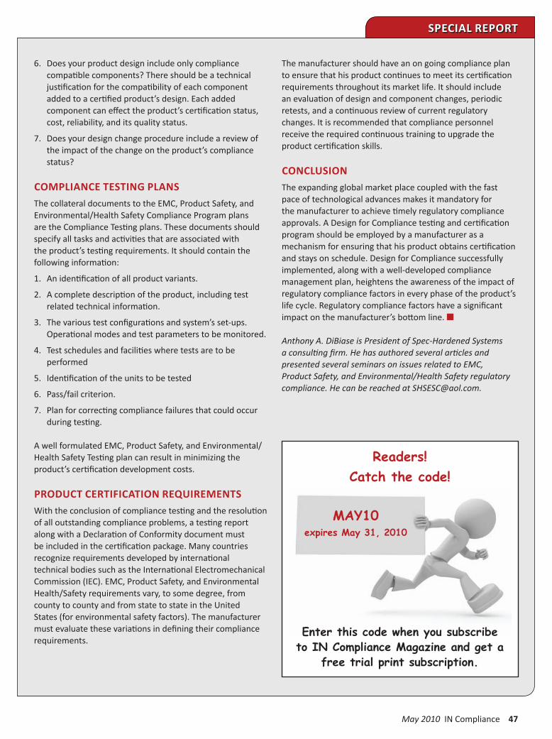
May 2010 IN Compliance 47
SPECIAL REPORT
6. Does your product design include only compliance compatible components? There should be a technical justification for the compatibility of each component added to a certified product’s design. Each added component can effect the product’s certification status, cost, reliability, and its quality status.
7. Does your design change procedure include a review of the impact of the change on the product’s compliance status?
COMPLIANCE TESTING PLANSThe collateral documents to the EMC, Product Safety, and Environmental/Health Safety Compliance Program plans are the Compliance Testing plans. These documents should specify all tasks and activities that are associated with the product’s testing requirements. It should contain the following information:
1. An identification of all product variants.
2. A complete description of the product, including test related technical information.
3. The various test configurations and system’s set-ups. Operational modes and test parameters to be monitored.
4. Test schedules and facilities where tests are to be performed
5. Identification of the units to be tested
6. Pass/fail criterion.
7. Plan for correcting compliance failures that could occur during testing.
A well formulated EMC, Product Safety, and Environmental/Health Safety Testing plan can result in minimizing the product’s certification development costs.
PRODUCT CERTIFICATION REQUIREMENTSWith the conclusion of compliance testing and the resolution of all outstanding compliance problems, a testing report along with a Declaration of Conformity document must be included in the certification package. Many countries recognize requirements developed by international technical bodies such as the International Electromechanical Commission (IEC). EMC, Product Safety, and Environmental Health/Safety requirements vary, to some degree, from county to county and from state to state in the United States (for environmental safety factors). The manufacturer must evaluate these variations in defining their compliance requirements.
The manufacturer should have an on going compliance plan to ensure that his product continues to meet its certification requirements throughout its market life. It should include an evaluation of design and component changes, periodic retests, and a continuous review of current regulatory changes. It is recommended that compliance personnel receive the required continuous training to upgrade the product certification skills.
CONCLUSIONThe expanding global market place coupled with the fast pace of technological advances makes it mandatory for the manufacturer to achieve timely regulatory compliance approvals. A Design for Compliance testing and certification program should be employed by a manufacturer as a mechanism for ensuring that his product obtains certification and stays on schedule. Design for Compliance successfully implemented, along with a well-developed compliance management plan, heightens the awareness of the impact of regulatory compliance factors in every phase of the product’s life cycle. Regulatory compliance factors have a significant impact on the manufacturer’s bottom line. n
Anthony A. DiBiase is President of Spec-Hardened Systems a consulting firm. He has authored several articles and presented several seminars on issues related to EMC, Product Safety, and Environmental/Health Safety regulatory compliance. He can be reached at [email protected].
Enter this code when you subscribeto IN Compliance Magazine and get a
free trial print subscription.
MAY10expires May 31, 2010
Readers!Catch the code!
48 IN Compliance May 2010 www.incompliancemag.com
CALENDAR
Seminars and TrainingMay 3Circuit-to-Circuit InterferenceSILENTChelmsford, MAwww.incompliancemag.com/events/100503_1
May 3 - May 4 Cost-Effective EMC Design for Compliance and Financial Benefits EMC TechnologiesSydney, Australia www.incompliancemag.com/events/100503_2
May 4 Electronic Product Design and Retrofit for EMC SILENTChelmsford, MAwww.incompliancemag.com/events/100504_1
May 4 Printed Circuit Design for EMC SILENTChelmsford, MAwww.incompliancemag.com/events/100504_2
May 4 Mechanical Design for EMC SILENTChelmsford, MAwww.incompliancemag.com/events/100504_3
May 4 - May 6 ESD Association NE Local Chapter Regional Tutorial Program ESD AssociationTewksbury, MAwww.incompliancemag.com/events/100504_4
May 5Basic and Advanced PCB Design for EMC and Signal IntegrityEMC TechnologiesSydney, Australiawww.incompliancemag.com/events/100505 May 6 Medical EMC: IEC/EN 6601-1-1 (AS/NZS 3200.1.2) EMC TechnologiesSydney, Australia www.incompliancemag.com/events/100506_1
May 6 Close-Field Probing for Emissions and Immunity EMC TechnologiesSydney, Australia www.incompliancemag.com/events/100506_2
May 7 Northwest EMC Seminar: A Day of Technical PresentationsNorthwest EMC, Inc. Brooklyn Park, MNwww.incompliancemag.com/events/100507_1
May 7 EMC Design of Switch-Mode Power Converters EMC TechnologiesSydney, Australia www.incompliancemag.com/events/100507_2
May 10 Drive a Spectrum Analyzer Like an Expert for EMC Test and Troubleshooting SILENTChelmsford, MAwww.incompliancemag.com/events/100510_1
May 10 International Approvals Round Table Complimentary InvitationTUV RheinlandRochester, NY www.incompliancemag.com/events/100510_2
May 11 EMC for Electrical Engineers Working in the Real-World IEEE EMC Chicago ChapterItasca, ILwww.incompliancemag.com/events/100511_1
May 2010 IN Compliance 49
CALENDAR
May 11 - May 12 Lightning Protection Installation Standard Review UL UniversityDenver, COwww.incompliancemag.com/events/100511_2
May 11 Understanding Ground Resistance Testing AEMC InstrumentsMinneapolis, MNwww.incompliancemag.com/events/100511_3
May 12 - May 13 Test, Measurement and Laboratory Use Equipment: Designing for Compliance to UL 61010-1 UL UniversitySan Jose, CA www.incompliancemag.com/events/100512_1
May 12 Test Area and Personnel/Common Electrical Product Safety Tests Seminar Associated Research, Inc. Lake Forest, ILwww.incompliancemag.com/events/100512_2
May 12 International Approvals Round Table Complimentary Invitation TUV RheinlandPittsburgh, PA www.incompliancemag.com/events/100512_3
May 13Data Acceptance Program and ISO/IEC 17025 Requirements and Implementation UL UniversityDallas, TXwww.incompliancemag.com/events/100513
May 18 - May 21 MIL-STD-461F: Methods and Procedures WL Academy Gaithersburg, MDwww.incompliancemag.com/events/100518
May 19International Approvals Round Table Complimentary InvitationTUV RheinlandLos Angeles, CAwww.incompliancemag.com/events/100519_1
May 20 International Approvals Round Table Complimentary Invitation TUV RheinlandPhoenix, CA www.incompliancemag.com/events/100520
May 25 - May 27 Photovoltaics: Overview of UL 173 and IEC 61730 UL UniversitySan Jose, CA www.incompliancemag.com/events/100525_1
May 25 International Approvals Round Table Complimentary Invitation TUV RheinlandPhiladelphia, PA www.incompliancemag.com/events/100525_2
May 25 Technology Solutions for Vietnam’s Sustainable Economic Development Goals Washington LaboratoiesHanoi, Vietnamwww.incompliancemag.com/events/100525_3
continues on page 50
50 IN Compliance May 2010 www.incompliancemag.com
A.H. Systems, Inc. . . . . . . . . . . . . . . . . . .23
AR. . . . . . . . . . . . . . . . . . . . . . . . . . . . . . .13
Braden Shielding Sytems . . . . . . . . . . . .C4
CITEL, Inc. . . . . . . . . . . . . . . . . . . . . . . . .29
Com-Power Corporation . . . . . . . . . . . .C2
E. D. & D., Inc. . . . . . . . . . . . . . . . . . . . . .19
EM Test USA Inc. . . . . . . . . . . . . . . . . . . .15
EMCC Dr Rasek . . . . . . . . . . . . . . . . . . . .11
ETS-Lindgren . . . . . . . . . . . . . . . . . . . . . .C3
IEEE EMC 2010 . . . . . . . . . . . . . . . . . . . .31
Intertek . . . . . . . . . . . . . . . . . . . . . . . . . .17
Panashield Inc. . . . . . . . . . . . . . . . . . . . .7
Spira Manufacturing Corporation . . . . .27
CALENDAR
May 26 - May 27 The CE Marking: Strategies for European Compliance UL UniversityNorthbrook, ILwww.incompliancemag.com/events/100526
May 27 Technology Solutions for Vietnam’s Sustainable Economic Development Goals Washington LaboratoriesHo Chi Minh City, Vietnamwww.incompliancemag.com/events/100527_1
WebinarsMay 19Earth and Enclosure Leakage TestingAssociated Researchwww.incompliancemag.com/events/100519_2
May 25 The Good, the Bad and the Improvements in CDM ESD Testing ESD Associationwww.incompliancemag.com/events/100525_4
May 27 Electrostatic Attraction ESD Associationwww.incompliancemag.com/events/100527_2
Tradeshows & SymposiumsMay 10 - May 134th Annual International Electrostatic Discharge WorkshopESD AssociationTutzing, Germanywww.incompliancemag.com/events/100510_3
May 11 12th Annual Chicago EMC MiniSymposium IEEE EMC Chicago ChapterItasca, ILwww.incompliancemag.com/events/100511_4
May 23 - May 28 IEEE MTT 2010 International Microwave Symposium Anaheim Convention Center IEEE MTT-Swww.incompliancemag.com/events/100523
ADVERTISERS
Advertiser Page Advertiser Page