Embed Size (px)
Citation preview
April 25, 2005
LHCb-Note 2005-025
Draft Version 2.0
The LHCb Outer Tracker Front End Electronics
A.Berkien, H.Deppe, B.Hommels, J.Knopf, M.Nedos, A.Pellegrino, T.Sluijk,J.Spelt, U.Stange, U.Trunk, U.Uwer, D.Wiedner, A.Zwart
Abstract
This note provides an overview of the front-end electronics used to readout thedrift-times of the LHCb Outer Tracker straw tube chambers. The main functionalcomponents of the readout are the ASDBLR ASIC for amplification and signaldigitization, the OTIS ASIC for the time measurement and for the L0 buffering,and the GOL ASIC to serialize the digital data for the optical data transmission.The L1 buffer board used to receive the data which is sent via the optical link isa common LHCb development and is not described here. This note supersedesan earlier document [1].
1 The LHCb Outer Tracker
The LHCb Outer Tracker (OT) [2] is a straw tube drift-chamber detector andconsists of 3 stations, each with a surface of 6× 5m2. A station has four stereo-layers. Each stereo-layer consists of 2 × 9 chamber modules with a width of34 cm and a length of 5 m. The modules are electrically subdivided in an upperand lower section.Figure 1 shows a schematic xy-view of an OT chamber. To keep the materialin the center of the detector acceptance small, mechanical supports as well asread-out and service electronics must be placed at the outer edges of the detectorlayers.The detector modules comprise 256 single 2.5 m long straw tubes with a diameterof 5 mm. The tubes are glued to 2 supporting panels from which the gas-tightdetector modules are built. The straws of the upper and lower panel section arenot connected and form separate readout channels. In this way the high particlerate, expected for the module center, is distributed on upper and lower channels.The module width corresponds to 64 straws (34 cm). In total, the OT has about55000 channels.
1.1 Straw tubes
The used drift-tubes have a diameter of 5 mm and an anode wire of 25µm. Ascounting gas we envisage to use Ar/CO2 (baseline) or Ar/CF4/CO2. Table 1summarizes the working point and the maximum drift-time for the two countinggases.
Signals for different counting gasesAr/CO2/CF4 Ar/CO2
Operating Voltage 1570 V 1550 VMax. Drift-time 37 ns 44 nsSignal rise time < 4 nsCharge deposition by MIP 220 fC
Table 1: Operating voltage and signal properties for two counting gas options(gas gain ∼35000).
The straw (cathode) is a laminate of 3 different materials. Kapton XC-160(25% of volume carbon doped Kapton) with a surface conductivity of 200 Ω/(equivalent to a resistivity of 60 kΩ/m) is used as inner cathode material. Toimprove the signal transmission of the fast signal part, and to reduce cross-talkbetween neighboring straws a 12.5µm thick (skin depth at 40 MHz is ∼ 13µm)
1

Figure 1: Outer Tracker chambers: readout and service electronics is placed atthe outer edges of the detector.
aluminium foil is used as outside layer. As it was necessary to introduce anadditional layer of non-conductive Kapton in between to ensure gas tightnessof the straws, the aluminum foil is pre-laminated to the non-conductive Kaptonfoil. Straws are wound using this pre-laminate together with the Kapton XC foil.The non-conductive foil isolates the aluminium shield from the inside cathodefoil. The connection of both foils to the chamber reference ground is addressedbelow. The electrical properties for the drift-tubes have been extensively studied[3]. Important properties are summarized in Table 2.While the front-end electronics which is connected to the readout side of thestraw tube matches the straw impedance, the inner end of the straw is left open,i.e. signals are not terminated at this side.
2

Straw electrical propertiesCharacteristic Impedance 316 ΩCapacitance 10 pF/mSignal propagation 3.8 ns/mAnalog Cross talk ≤ 0.5%
Table 2: Electrical properties of the drift-tubes (Kapton XC + aluminium straws)[3]: The quoted value for the impedance is not considering the frequency de-pendence of the ohmic resistance of the 25 µm anode wire (skin-effect). Thecross-talk number is given for the next neighbor.
1.2 Elements of the readout electronics
The drift-times of ionization clusters prodcued by through-going particles aremeasured for every drift-tube. Reference for the time measurement is the beamcrossing (BX) signal. Hit times are digitized for every bunch crossing (25 ns)and stored in a digital pipeline to await the Level-0 (L0) decision. On a positiveL0 decision, the digitized data is transmitted via optical links to the Level-1 (L1)buffer boards, which are the front-end of the common readout-system.A schematics of the front-end electronics is shown in Fig. 2. The elements ofthe Outer Tracker specific readout-electronics are:
• Feedthrough board: This passive printed-circuit board (PCB) is part ofthe module. It provides the electrical connections to the straws. Moreoverit defines the reference ground for electronics and straws.
• High-voltage board: The board distributes the high-voltage to the strawchannels. It contains capacitors for the signal decoupling from the chamberHV. It is plugged directly to the feed-through board.
• ASDBLR board: The board carries two ASDBLR chips. The ASDBLRASIC is an 8-channel amplifier-shaper-discriminator with ion-tail cancella-tion and baseline restoration designed for the ATLAS TRT [4].
• OTIS board: Two ASDBLR boards are plugged to a common boardfor the time measurement. The board carries the OTIS, an 32-channelTDC-chip which especially designed for LHCb Outer Tracker [11]. On aL0 accept the OTIS provides the digital event data on a 8-bit differentialoutput.
• GOL/Aux board: 4 OTIS boards are connected to a GOL/Aux board.The GOL/Aux board [14] provides power, fast-control signals (BX clock,
3
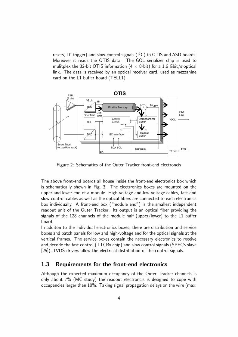
resets, L0 trigger) and slow-control signals (I2C) to OTIS and ASD boards.Moreover it reads the OTIS data. The GOL serializer chip is used tomulitplex the 32-bit OTIS information (4 × 8-bit) for a 1.6 Gbit/s opticallink. The data is received by an optical receiver card, used as mezzaninecard on the L1 buffer board (TELL1).
TDC +
ReadoutBuffer
DerandomizerBuffer
Pipeline MemoryTrigger
Hit
DriftTime
DLL
DAC
Fine Time
ControlCircuit
I2C Interface
BX
SDA SCLnotReset
TTCrx
GbitLink
8
OTIS
Straw Tube(w. particle track)
32 ch
GOL
TTC
ASD(8 ch)
Figure 2: Schematics of the Outer Tracker front-end electroncis
The above front-end boards all house inside the front-end electronics box whichis schematically shown in Fig. 3. The electrronics boxes are mounted on theupper and lower end of a module. High-voltage and low-voltage cables, fast andslow-control cables as well as the optical fibers are connected to each electronicsbox individually. A front-end box (“module end”) is the smallest independentreadout unit of the Outer Tracker. Its output is an optical fiber providing thesignals of the 128 channels of the module half (upper/lower) to the L1 bufferboard.In additon to the individual electronics boxes, there are distribution and serviceboxes and patch panels for low and high-voltage and for the optical signals at thevertical frames. The service boxes contain the necessary electronics to receiveand decode the fast control (TTCRx chip) and slow control signals (SPECS slave[25]). LVDS drivers allow the electrical distribution of the control signals.
1.3 Requirements for the front-end electronics
Although the expected maximum occupancy of the Outer Tracker channels isonly about 7% (MC study) the readout electroncis is designed to cope withoccupancies larger than 10%. Taking signal propagation delays on the wire (max.
4
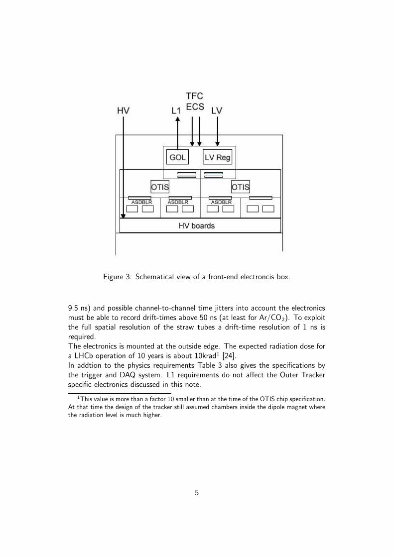
Figure 3: Schematical view of a front-end electroncis box.
9.5 ns) and possible channel-to-channel time jitters into account the electronicsmust be able to record drift-times above 50 ns (at least for Ar/CO2). To exploitthe full spatial resolution of the straw tubes a drift-time resolution of 1 ns isrequired.The electronics is mounted at the outside edge. The expected radiation dose fora LHCb operation of 10 years is about 10krad1 [24].In addtion to the physics requirements Table 3 also gives the specifications bythe trigger and DAQ system. L1 requirements do not affect the Outer Trackerspecific electronics discussed in this note.
1This value is more than a factor 10 smaller than at the time of the OTIS chip specification.At that time the design of the tracker still assumed chambers inside the dipole magnet wherethe radiation level is much higher.
5
Outer Tracker Requirementsmax. drift-time in ArCF4CO2 (ArCO2) 37 ns (44 ns)max. occupancy 10%double hit sequence < 20 nsradiation dose (10 years) < 10 kradtemp. range 15 ... 70o CTDC resolution < 1 ns
DAQ/L0 requirementsmax. L0 rate 1.1 MHzL0 Latency / Pipeline 4.0 µs / 160 eventsBX Counter 12 bitmax. readout time 900 nssize of Derandomizer ≥ 16
Table 3: Outer Tracker and L0 trigger requirements for the front-end electronics.
2 Front-End Electronics Components
2.1 Module Shielding, Grounding and Feedthough boards
Module shielding: In addition to the alu shielding of the single straws it wasdecided to enclose the straws of a module by an additional Faraday shielding:The straw supporting panels, as well as the module side-walls carry a 12.5µmthick alu foil (skin depth at 40 MHz ∼ 13µm ). When gluing the box togetherthe side-wall shielding is connected electrically to the panel shields. The top andbottom sides of the module are electrically closed by the feed-though boards.The sensitivity to EMI was studied using a 27 MHz radio-transmitter and wasfound to be very low [8].
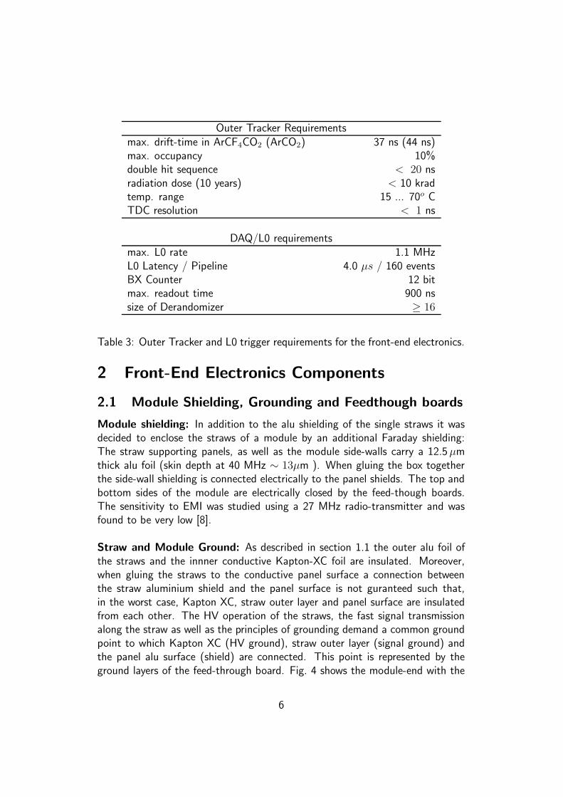
Straw and Module Ground: As described in section 1.1 the outer alu foil ofthe straws and the innner conductive Kapton-XC foil are insulated. Moreover,when gluing the straws to the conductive panel surface a connection betweenthe straw aluminium shield and the panel surface is not guranteed such that,in the worst case, Kapton XC, straw outer layer and panel surface are insulatedfrom each other. The HV operation of the straws, the fast signal transmissionalong the straw as well as the principles of grounding demand a common groundpoint to which Kapton XC (HV ground), straw outer layer (signal ground) andthe panel alu surface (shield) are connected. This point is represented by theground layers of the feed-through board. Fig. 4 shows the module-end with the
6
feed-through boards and the ground connections.
Figure 4: Module end with the feed-through defining the module ground.
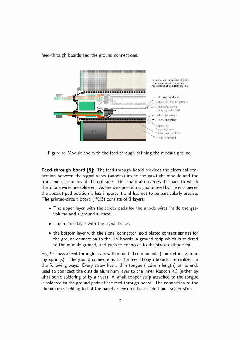
Feed-through board [5]: The feed-through board provides the electrical con-nection between the signal wires (anodes) inside the gas-tight module and thefront-end electronics at the out-side. The board also carries the pads to whichthe anode wires are soldered. As the wire position is guaranteed by the end-piecesthe absolut pad position is less important and has not to be particularly precise.The printed-circuit board (PCB) consists of 3 layers:
• The upper layer with the solder pads for the anode wires inside the gas-volume and a ground surface.
• The middle layer with the signal traces.
• the bottom layer with the signal connector, gold plated contact springs forthe ground connection to the HV boards, a ground strip which is solderedto the module ground, and pads to conncect to the straw cathode foil.
Fig. 5 shows a feed-through board with mounted components (conncetors, ground-ing springs). The gound connections to the feed-though boards are realized inthe following ways: Every straw has a thin tongue ( 12mm length) at its end,used to conncect the outside aluminum layer to the inner Kapton XC (either byultra sonic soldering or by a rivet). A small copper strip attached to the tongueis soldered to the ground pads of the feed-through board. The connection to thealuminium shielding foil of the panels is ensured by an additional solder strip.
7

Figure 5: Feed-through board.
The feed-through board defines the “module ground” and is used as reference forthe subsequent electronics. The ground connection to the HV board is ensuredby large surface spring contatcs.
2.2 HV Board
While the feed-through board is an integral part of the drift-chamber module, theHV board is not: two 32-channels HV boards are plugged to one feed-throughboard. For the HV signal connection SMD Samtec conncetors 2 are used. Thespring-contacts of the feed-through boards ensure good connection to the modulereference ground.The HV board supplies the 32 channels with a common HV. Pre-resistors of1 MΩ are used in front of every channel to decouple the anode from each otherand to avoid large currents in case of shorts in the drift-tubes. SMD ceramiccapacitors3 (330pF, 4kV max.), 4.6 × 2 × 1.5mm3 are used to decouple thechamber signals from the HV. The electronics scheme of 16 out of 32 channelsis shown in Fig. 6.The high channel density, the compact size of the HV capacitors (less than 4 mmbetween the two contacts of the capacitors) and the relatively large operatingvoltage (1550 V) demands additional insulation of the capacitors to avoid dis-charges across the capacitor surface. This is in particular necessary as the HV
22/10 inches, every second contact is removed3JOHANSON 302R29W331KV4E
8

Figure 6: HV board schematics for 16 out of the 32 channels per board.
boards will be operated in air (early prototypes of the HV boards showed leakagecurrents of up to 100 nA/channel during test beams at CERN).In insulation of the capacitors is achieved by embedding the capacitors in themulti-layer PCB as shown in Fig. 7. The casting process should avoid stresson the ceramic capacitors. As it is difficult to reach the area underneath thecapacitor pick-and-place paste must be used to place the capacitors and to avoiddischarges in this area.After refining the production process a prototype series of 80 boards (2560 chan-nels) has been produced. A large series test of the 2560 channels (24 h) as wellas a long-term test (23 days) of 15 boards have been performed. Both tests didnot show any problem4.
2.3 ASDBLR Board
ASDBLR ASIC
The ASDBLR ASIC is an eight-channel amplifier-shaper-discriminator with base-line restoration designed for the read-out of the ATLAS Transition Radiation
4In the large series test only one single capacitor showed an unacceptable high current.
9
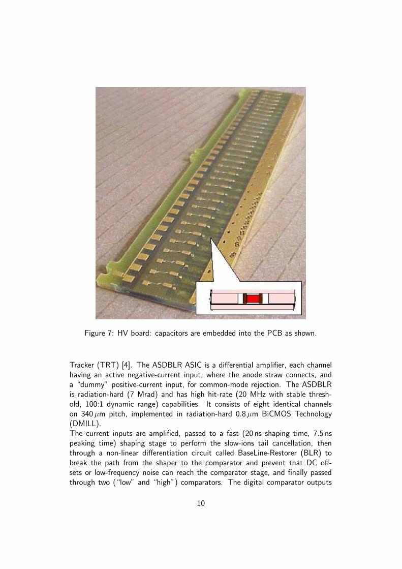
Figure 7: HV board: capacitors are embedded into the PCB as shown.
Tracker (TRT) [4]. The ASDBLR ASIC is a differential amplifier, each channelhaving an active negative-current input, where the anode straw connects, anda “dummy” positive-current input, for common-mode rejection. The ASDBLRis radiation-hard (7 Mrad) and has high hit-rate (20 MHz with stable thresh-old, 100:1 dynamic range) capabilities. It consists of eight identical channelson 340µm pitch, implemented in radiation-hard 0.8µm BiCMOS Technology(DMILL).The current inputs are amplified, passed to a fast (20 ns shaping time, 7.5 nspeaking time) shaping stage to perform the slow-ions tail cancellation, thenthrough a non-linear differentiation circuit called BaseLine-Restorer (BLR) tobreak the path from the shaper to the comparator and prevent that DC off-sets or low-frequency noise can reach the comparator stage, and finally passedthrough two (“low” and “high”) comparators. The digital comparator outputs
10
are summed as current steps to form a differential ternary output with sharp turn-on (1 ns risetime). For the application in Outer Tracker only the “low” (tracking)threshold comparator is used. It has been measured that for the Outer Trackerstraw signal the average charge collection efficiency is about 8%.It operates on ±3 V supplies with a typical power requirement of about 40 mWper channel (the exact value depending on the programmed value of the ternaryand monitor outputs). A detailed description of the chip design, constructionand performance can be found in Ref. [4]. Studies of the operational propertiesof the ASDBLR chip for the readout of Outer Tracker straw tubes can be foundin Refs. [3, 6, 8, 9].
ASDBLR board
The essential function of the ASDBLR Board [7] is to host two ASDBLR preamplifier-discriminator ASICs. the design principles of the ASDBLR Board are largely basedon the results of the ASDBLR studies done for the Outer Tracker. The choice ofplacing two ASDBLRs per board is a trade-off between two extreme scenarios:having eight ASDBLR’s and two OTIS’s on a single FE board, and having onesingle ASIC per board.The amplifier input sees the contribution of several parasitic capacitances. Keep-ing all traces and especially the sensitive input lines as short as possible reducesthe capacitive and inductive cross talk. Additionally, to reduce the channel-to-channel cross-talk, each signal pin on the connector is surrounded by ground pinson either side. Moreover, the ground planes of the HV and ASDBLR Boards aredirectly coupled over the full board widths via special contact springs. The ampli-fier input noise can be characterized as follows [4]: ENC ' 2100 e+ 145 e/pF×Cin [pF] [9]. The total contribution of the FE Electronics has been measuredto be about 20 pF (7 pF from the traces of the Feed-Through Board, 7 pF fromthose of the HV Board, and 6 pF from the ASDBLR Board traces and extra pro-tection circuitry). Therefore the total input noise contributed by the electronicsis about 5000 e ' 0.8 fC, consistsent with our measurement [9], which mustbe compared to an effective signal size of ∼20 fC (taking the charge collectionefficiency of about 8% into account) [10].The main contribution to the power consumption on the ASDBLR board isexpected to come from the ASDBLR ASIC. This has been estimated to beδP+ ' δP− ' 80 mA × 3 V = 240 mW, which gives a total of 960 mW perASDBLR board. The ASDBLR Board has been provided with a heat-spreadinglayer in the PCB, to which heat-conducting mounting posts are coupled. Thesecooling posts are then intended to be coupled to the internal cooling chassis ofthe front-end electronics box. Tests with prototypes of the ASDBLR boards (seebelow) showed that the ASDBLR chip internal temperature was less than 25 oC
11

above the cooling-surface temperature (∼ 20 oC).
2.4 OTIS and OTIS Board
OTIS TDC Chip
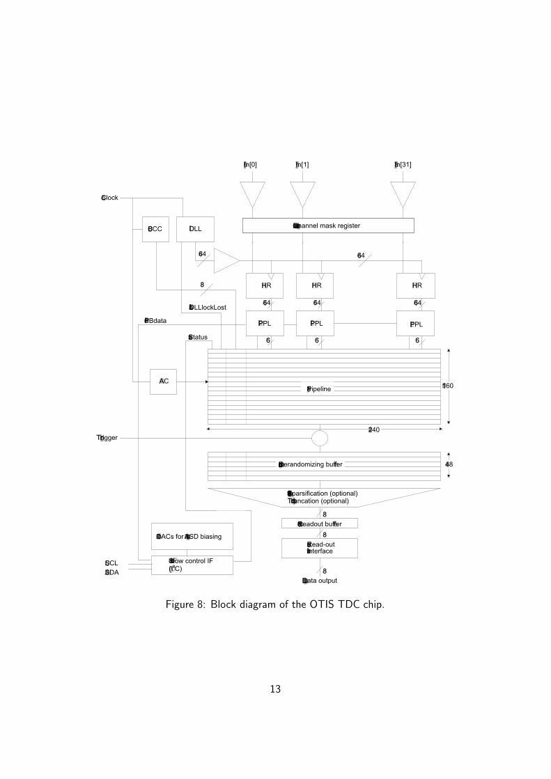
The OTIS chip [11] is developed for the readout of the LHCb Outer Trackerstraw tubes. The chips operates synchronous to the 40 MHz LHC clock. Maincomponents of the chip are:
• the TDC core, consisting of a DLL, hit register and hit decoder
• the L0 pipeline buffer together with the derandomizing buffer to cover theL0 latency and to cope with fluctuations of the trigger rate
• the control logic for the trigger and memory management and to preparethe output data
• the I2C interface for setup and slow control
In addition the chip comprises 4 DACs to provide the threshold voltages forthe ASD discriminator chips. The block diagram of the OTIS chip is shown inFigure 8. The chip serves 32 input channels (LVDS) and provides 8 bit wide dataoutput (differential CMOS).TDC core: For the time measurement a DLL, consisting of a chain of 32 doublestaged delay elements, is used. The BX clock propagates through the chain. Aphase detector compares the delayed clock with the original one. Dependingon the observed phase shift a charge pump adjusts the voltage controlled delayelements until the phase difference vanishes. In this state the DLL is locked andthe DLL clock can be used as reference for the time measurements. To decreasethe uncertainty of the digitization the number of DLL tabs are doubled by usingboth stages of each of the 32 delay elements. The output of the DLL stages areused to clock 64 hit registers and to latch the the discriminated hit signal. Adecoder converts the status of the 64 registers into a 6 bit “fine time”.Pipeline and derandomizing buffer: Pipeline and derandomizing buffer arebuilt as arrays of dual ported SRAM cells. The memory dimensions are 164events x 240 bits and 48 events x 240 bits respectively. The depths of bothbuffers are thus larger than required by the L0 specifications.Control Algorithm: The control algorithm provides trigger and memory man-agement as well as the control of the data output stream. The hardware descrip-tion language Verilog was used to code the algorithm.Readout modes: On a positive L0 trigger the control algorithm can searchdetector hits in up 3 bunch crossings. In the multi BX modes not all possible hits
12
DLLBCC
Clock
6464
8
In[0] In[1] In[31]
64 64 64
6 6 6
HR HR HR
PPL PPL PPL
Trigger
Sparsification (optional)Truncation (optional)
Read-outinterface
Data output
AC160
240
48
É
É
É
Pipeline
Derandomizing buffer
Readout buffer
Slow control IF(I C)
2
DACs for ASD biasing
Channel mask register
DLLlockLost
8
8
8
Status
PBdata
SCL
SDA
Figure 8: Block diagram of the OTIS TDC chip.
13
can be transmitted within the required 900 ns readout time. Therefore, thereare 2 different readout modes to cope with this situation:
1. every channel, whether hit or not, appears in the readout. Only the firsthit is transmitted.
2. times are transmitted only for channels with hits. A 32-bit hit mask forevery bunch crossing indicates the channels with hits. If the maximumnumer of possible hits is reached the event is truncated.
Test modes: On a power-up reset a memory test is executed. The chip allowsfurther to write known hit/time patterns into the pre-pipeline register.Slow control: The slow-control interface to the chip is implemented using I2C.The interface allows to read and write the control registers, to load the pre-pipeline register with test-data (play-back mode), to read an accepted eventfrom the derandmoizing buffer (important for laboratory usage of the chip), andto set the 4 DACs used for the threshold setting of the 4 ASDBLR chips (seebelow).
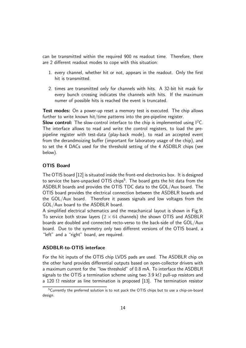
OTIS Board
The OTIS board [12] is situated inside the front-end electronics box. It is designedto service the bare-unpacked OTIS chips5. The board gets the hit data from theASDBLR boards and provides the OTIS TDC data to the GOL/Aux board. TheOTIS board provides the electrical connection between the ASDBLR boards andthe GOL/Aux board. Therefore it passes signals and low voltages from theGOL/Aux board to the ASDBLR board.A simplified electrical schematics and the meachanical layout is shown in Fig.9.To service both straw layers (2 × 64 channels) the shown OTIS and ASDBLRboards are doubled and connected recto-verso to the back-side of the GOL/Auxboard. Due to the symmetry only two different versions of the OTIS board, a“left” and a “right” board, are required.
ASDBLR-to-OTIS interface
For the hit inputs of the OTIS chip LVDS pads are used. The ASDBLR chip onthe other hand provides differential outputs based on open-collector drivers witha maximum current for the “low threshold” of 0.8 mA. To interface the ASDBLRsignals to the OTIS a termination scheme using two 3.9 kΩ pull-up resistors anda 120 Ω resistor as line termination is proposed [13]. The termination resistor
5Currently the preferred solution is to not pack the OTIS chips but to use a chip-on-boarddesign.
14
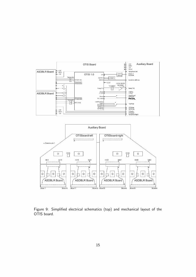
Figure 9: Simplified electrical schematics (top) and mechanical layout of theOTIS board.
15

Figure 10: Layout of the GOL/Aux board.
leads to a maximum signal swing 48 mV at the LVDS pads sufficiently large toswitch the inputs. A detailed definition of the ASDBLR-to-OTIS interface canbe found in Ref. [13].
2.5 GOL/Aux Board
The GOL/Auxiliary board [14] is connected to 4 OTIS boards. It serializes theTDC Data and outputs the data to an optical link. The board supplies theOTIS boards with low voltage, fast control and slow control signals. It providesvoltage and temperature sensing pins. A layout of the GOL/Aux board is shownin Fig. 10For data serialization the GOL/Aux board uses the GOL chip [15]. The chip isa CERN EP development in rad-hard 0.25 µm technology. It serializes the 32data-bits coming from the four OTIS boards on one module end. The data isencoded according 8/10 bit Giga-bit ethernet encoding standard [16], resultingin a 1.6 Gbit/s output rate. The serial data is driven into a VCSEL diode coupledto 50/125 µm optical fiber using a SMA connection.
16
The GOL serializer requires for the clock signal (40 MHz) a jitter of less than100 ps (peak-peak). The QPLL chip (CERN EP) is used to stabilize the clocksignal received from the the service box (TTCrx chip) . The QPLL uses avoltage controlled quartz oscillator (4× LHC frequency) . The filtered clock isalso supplied to the OTIS boards.All fast control signals such as clock, L0 Trigger Accept, L0 Reset, Bunch CountReset, Event Count Reset, and test-pulse signals for odd and even preamplifierchannels (large and small apmlitudes) are distributed as LVDS signals. Slowcontrol signals are distributed over I2C bus to the OTIS TDC and GOL serializerchips. A selectable switch allows to set the I2C and the OTIS IDs6. In additionthe board allows temperature and voltage sensing.All electrical signals, i.e. fast- and slow-control signals, test pulses and senselines are supplied by a standard SCSI cable. The connection is a point-to-pointconnection from the dirstribution box to the individual front-end boxes. Todecouple possible voltage drops all signals are distributed as LVDS signals. Thisincludes the I2 bus, where a differential distribution as suggested by Philips isused.Radiation hard power regulators developed at CERN supply the low voltage.Positive types L4913 deliver +3 V for the ASDBLR and +2.5 V for GOL, OTISand QPLL. One negative type L7913 are used for the -3 V of the ASDBLR. Thepower is derived from incoming ±6 V. The power regulators are a majort heatsource and are therefore mounted directly on the cooling structure.
2.6 Optical Link
For the transmission of the serialized detector data from the GOL/Aux board tothe L1 buffer board an optical link is used.The serialized GOL output (1.6 Gbit/s, 8/10 bit Giga bit ethernet standard [16])drives a commercial VCSEL diode (ULM Photonics), which was tested to beradiation tolerant by the LHCb Inner Tracker group. For optical transmission theVCSEL diode is connected to an optical fiber. The fiber consists of 4 sections.A 50/125 µm multi-mode fiber with SMA connectors runs to the optical patch-panel on the detector frame. At the patch panel the 9 fibers of one quarter layerare fed into a 12 fiber optical ribbon cable, also 50/125 µm. The ribbon cable isnot directly goin to the trailer but to an optical patch panel located in the concrettunnel underneath the detector. The 12-fold fibers are connected to a 96-foldoptical cable bundel which bridges the ∼100 m distance to the trailer. Hereanother patch panel is located, close to the Trigger ELectronics and L1 boards
6The lowest 2 bits of the OTIS IDs are hardwired on the GOL board and therfore notselectable.
17
(TELL1) [17]. A short optical ribbon connects the patch panel to the opticalreceiver cards on the TELL1, allowing an easy exchange of fiber destinationswithout exposing the long ribbon cable to mechanical stress.Two optical receiver cards (O-Rx Cards) can be mounted on one TELL1 board.Each O-RxCard citeORx carries one commercial 12 fiber optical receiver [19]and twelve de-serializer chips [20], allowing a maximum of 24 optical inputs foreach TELL1 board. The de-serialized data is synchronized and processed on theTELL1 board with the help of FPGAs. Details on the link synchronization canbe found in Ref. [21].A transmission test which was involving all link compoenents of the Outer Tracker(GOL/Aux, optical fibers, O-Rx cards) resultes in a limit for the error probabilityof less than 10−15.As the optical link is common for the LHCb Inner Tracker, VETO, Outer Trackerand possibly further subsystems, many components such as fibers, VCSEL diodesand the O-RxCards are the same for these sub-detectors.Apart from the optical data link described here, the Timing and Fast Control(TFC) system [22] will utilize optical data transmission. For the TFC systemdifferent optical components are used.
2.7 Front-end electronics box
Assembly and Maintenance
The front-end boards (4 HV boards, 8 ASDBLR boards, 4 OTIS boards and 1GOL/Aux board) are mounted in a mechanical box [23]. The box constructionprovides a support frame to carry the boards. The support frame serves atthe same time a heat-conductor and is in thermal contact with all major heatsources. The complet construction is enclosed with metal (ground) cover sheets.The front and the side view of an assembled box is shown in Fig. 11. The onlyboard which sticks out of the construction is the GLO/Aux board, which alsocarries all the interface connections.The assembled electronics box is an independent unit and is plugged to the feed-through boards of the module. As the mounting of the box including the precisepositioning of the connectors 128 pins between feed-through and HV boards isdifficult, a mechanical guidances is used. Screws will allow safe connection anddisconnection of the box.As the boxes are independent units they can be tested before installation. Ifreadout and service cables are properly foreseeen the installation of the boxes onthe final detectos can therefore take place independently of the frame assembly.If service of electronic components of the box becomes necessary, the whole boxmust be dismounted and opened.
18

Figure 11: Assembly of the front-end electronics boards: front and side view.
In case of broken or hot wires we can disconnect one of the 4 HV connections(corresponding to 32 channels) remotely in the counting room. During chambermaintenance one can disconnect the malfunctioning wires inidividually on thefeed-through boards.
Cooling
The front-end electronics and in particular the low-voltage regulators will dissipateabout 25 W per front-end box [26, 27]. Multiplied with the total number ofreadout boxes (432) the power consumption results in a total heat production ofabout 10 kW for the total detector. It is not possible to release the heat into theexperimental hall. Moreover the boxes are densly packed on the frames. Watercooling was therefore considered at an early stage of the design.The active electronics boards are designed that the heat sources are in thermalcontact (directly or using heat-spreading PCB layers of 100 µm thickness) withthe cooling chassis of the front-end electronics box. The main cooling plate ofthe electronics box will be mounted against a water-cooled frame.A cooling test with a thermally insulated front-end box has been done: Only themain cooling plate of the electronics box was cooled with air at room temperature
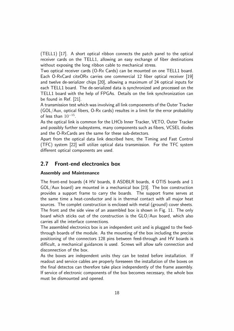
19
(∼ 20 oC). Fig. 12 summarizes the temperatures measured at thermal equilibriumfor the different parts of the front-end electronics. The equilibrium temperatureof the cooling plate was 35 oC. The highest temperature in the box was measuredwith 52 oC on the OTIS chip. For the amplifier chips values of about 42 oC havebeen measured. The temperatures of all deivices are only between 8 and 17degrees higher than the one of the cooling plate demonstrating the effectivenessof the cooling design. Moreover the absolute temeperature of the all boardswill decrease when the cooling plate is thermally connected to the water cooledsystem.
Figure 12: Cooling tests of the front-end electronics. The indicated temperatureshave been measured when the box was encloded with thermal insulation and onlythe cooling plate was cooled.
3 Control and Services
Each of the three Outer Tracker stations consist of four double-layers of strawtubes arranged in a XUVX sequence. Pairs of these planes (XU and VX) are
20
mounted onto frames that can be slided in two halves from and to the beam-pipe, like curtains. Per stereo-layer each detector “curtain” carries nine front-endelectronics boxes on the top and 9 boxes on the bottom of the curtain. Thisresults in a total of 36 Front End boxes per detector curtain. The front-endboxes have connections to the power supplies (High Voltage and Low Voltage),the Experiment Control System (ECS), and the Timing and Fast Control (TFC).In addition, optical fibers carry the data from each Front End box from thedetector to the counting room. The distribution and control boxes will providethe interface to all these services. Since each detector curtain is a unit withindependent movements, distribution and control boxes are foreseen at eachcorner of the detector curtain, as shown in Fig. 13.On each corner the following distribution and control boxes are mounted:
• High Voltage Distribution Box: The HV supply for the 128 straw-tubechannels per front-end box are subdivided in 4 groups with 32 straws each.Single HV cables (SHV connectors) are used to supply the HV. The 2×36connections for the top or the bottom arm of the curtain are connected toan HV distribution box, which is connected to multipin (56) long-distanceHV cables.
• Low Voltage Distribution Box: A Front End box typically draws a cur-rent of 2.6 A from the positive power supply and 0.9 A from the negativepower supply. For one detector curtain, this adds up to a current of 93.6 Afor the +6V supply and 32 A for the -6V supply. The Low Voltage Dis-tribution Box will provide the interface to the LV supply for 18 front-endboxes.
• Optical Fiber Panel: The digitized data is sent via 12-fold optical cablesto the optical receiver cards of the L1 buffer boards. In our scheme oneoptical ribbon cables serves the 9 front-end boxes of a stero-layer. Fourribbon cables are routed to a fiber panel which is mounted on the detectorcurtain.
• Control Box: For the distributes of TFC and ECS signals to and fromthe front-end boxes. Point-to-point connections are used to connect thefront-end boxes via commercial SCSI cables to the control box. All signalsare run as LVDS signals which decouples the front-end boxes from commonmodes.
21

lControl Box
HV Box
LV Box
Figure 13: Schematic view of services: Control (TDC+ECS) Low-voltage, high-voltage.
4 Detector Grounding
For a single module the reference ground of electronics and HV is the ground ofthe electronics box which is defined by the feed-through board. As all modulesare mechanically and electrically connected to the curtain frame made out ofaluminium, it is this frame which will work as the chamber ground referencepoint. Except a single connection to the “safety ground” of the experimentalhall, the frame will be kept floating:
• Gas and water pipes must be insulated from the frame.
• Connected low voltage power supplies are kept floating in the countingrooms.
• For the HV distribution, supplies with floating outputs are used. Theground shield of the HV lines are tied to the safety ground using a special“ground fault circuitry” in the counting room.
• Slow-Control and Fast-Control systems will be electrically decoupled.
A detailed description of the foreseen grounding scheme can be found in Ref. [30].
22

References
[1] M. Feuerstack-Raible et al., The LHCb Outer Tracker readout electronics,LHCb note LHCb-2001-013.
[2] LHCb Collaboration, LHCb Outer Tracker – Technical Design Report,CERN, Sep. 2001, LHCC/2001-024.
[3] V. Gromov and T. Sluijk, Electrical Properties of various types of strawtubes considered for the LHCb Outer Tracker, LHCb Technical Note LHCb-2001-001.
[4] R. Bevensee et al., IEEE (1996) Trans. on Nucl. Sci., Vol. 43, 1725;N. Dressnandt et al., ‘Implementation of the ASDBLR Straw Tube ReadoutASIC in DMILL Technology”, IEEE (2000) Trans. on Nucl. Sci., Vol. 48,1239;M. Newcomer and A. Romaniouk, ASDBLR chip operational propertiesstudies at CERN. ATLAS Internal Note INDET-NO-122, 1996.http://www.hep.upenn.edu/atlas/asdblr/
http://www.quark.lu.se/~atlas/electronics/trt/chip asdblr.html
http://www.hep.upenn.edu/atlas/asdblr/presentations/prr/
DMILL Fabs.pdf
[5] S. Bachmann et al., Definition of Feed-trough and Splitting Boards, LHCbTechnical Note LHCb-2003-052;
[6] V. Gromov et al., Study of Operational Properties of the ASDBLR Chip forthe LHCb Outer Tracker,LHCb Technical Note LHCb-2000-054.
[7] A.Berkien, T.Sluijk, A.Zwart, “LHCb Outer Tracker FE Electronics –Prototype of the ASDBLR Board”, to appear as LHCb note;http://www.nikhef.nl/pub/experiments/bfys/lhcb/outerTracker/
Electronics/FE-Electronics/ASDBLR.pdf
[8] Y.Gouz et al., “Study of the Global Performance of the LHCb OT Front-EndElectronics Prototype”, LHCb Technical Note LHCb-2004-120.
[9] B.Hommels et al., “Noise Studies with the LHCb Outer Tracker ASDBLRBoard”, LHCb Technical Note LHCb-2004-117.
[10] With ∼35 primary electrons and a gas gain of 40000 one expects a totalsignal charge of 220 fC. According to measurements from ATLAS and mea-surements done by R.Ruschmann (Diploma thesis, University of Heidelberg,
23
Jan 2002) only a fraction of about 10% of the signal charge arrives duringthe 7.5 ns peaking time.
[11] H.Deppe et al., The OTIS Reference Manual – Version 1.2,http://wwwasic.kip.uni-heidelberg.de/lhcbot/secure/Specifications/
OTIS12-UserManual.pdf.H.Deppe et al., “Status Report for the Chip Review on June 5, 2003”,http://physi.uni-heidelberg.de/ uwer/lhcb/Otis/Overview.pdf
[12] A.Berkien, T.Sluijk, A.Zwart, “OTIS Board”, to appear as LHCb note;http://www.nikhef.nl/ albert/docu/otisboard/Otisboard.doc
[13] T. Sluijk and U. Uwer, OTIS-to-ASDBLR interface, to appear as LHCbTechnical Note;http://physi.uni-heidelberg.de/ uwer/lhcb/Electronics/Review/
otis2asd-specs.ps.
[14] D.Wiedner et al., Specification for a Prototype of the Auxiliary Board forthe Outer Tracker, LHCb Internal Note LHCb-2003-129.
[15] P. Moreira et al., GOL Reference Manual, Gigabit Optical Link Transmittermanual http://proj-gol.web.cern.ch/proj-gol/manuals.htm
[16] IEEE Std 802.3, 1998 Edition.
[17] G. Haefeli et al., TELL1 Specification for a common read out board forLHCb, LHCb Note LHCb-2003-007.
[18] D.Wiedner et al., Prototype for an Optical 12 input Receiver Card for theLHCb TELL1 Board, LHCb Internal Note LHCb-2003-137.
[19] SNAP12 12 channel pluggable optical module MSA, Specifications, Ap-pendix to the SNAP12 Multi-Source Agreement
[20] TLK 2501 – 1.6 to 2.5 GHz deserializer, Texas Instruments; Revision July2003; http://Jocus.ti.com/lit/ds/symlink/tlk2501.pdf.
[21] H.Deppe et al., Synchronization of the LHCb Outer Tracker Optical Links,to appear as LHCB note,http://physi.uni-heidelberg.de/ uwer/lhcb/Electronics/Review/
sync.ps.
[22] Jorgen Christiansen et al., TTCrx Reference Manual, A Timing, Trigger andControl Receiver ASIC for LHC Detectors
24
[23] A.Berkien et al., The Front Ende Electronics Box for the LHCb OuterTracker, LHCb note in preparation.
[24] G.Corti, L.Shekhtman, “Radiation Baackground in the LHCb Experiment”,LHCb-Note 2003-83.
[25] D. Breton and D. Charlet, “SPECS: The serial protocol for the ExperimentControl System of LHCb”, LHCb-Note 2003-004.D. Breton and D. Charlet, “Using the SPECS in LHCb”, LHCb-Note 2003-005.
[26] T.Sluijk et al., Power Consumption of the Outer Tracker Front-EndElectronics, Outer Tracker internal note.http://physi.uni-heidelberg.de/ uwer/lhcb/Electronics/Review/
power-consumption.ps.
[27] A.Berkien et al., Cooling Test of the FE electroncis box, in preparation.
[28] T.Sluijk and A.Zwart, Distribution-Boxes and Control-Boxes for the OuterTracker, to appear as LHCb note,http://physi.uni-heidelberg.de/ uwer/lhcb/Electronics/Review/
Distribution Box.pdf.
[29] U. Uwer and A. Zwart, Test Pulse System for the LHCb Outer TrackerDetector,http://physi.uni-heidelberg.de/ uwer/lhcb/Electronics/Review/
Test Pulse.pdf.
[30] T.Sluijk et al. Grounding and Shielding of the CERN LHCb Outer TrackerDetector, to appear as LHCb Technical Note;http://www.nikhef.nl/ toms/grounding/
Grounding-and-Shielding-of-the-Outer-Tracker-Detector.pdf.
25