Embed Size (px)
Citation preview

The following document contains information on Cypress products.
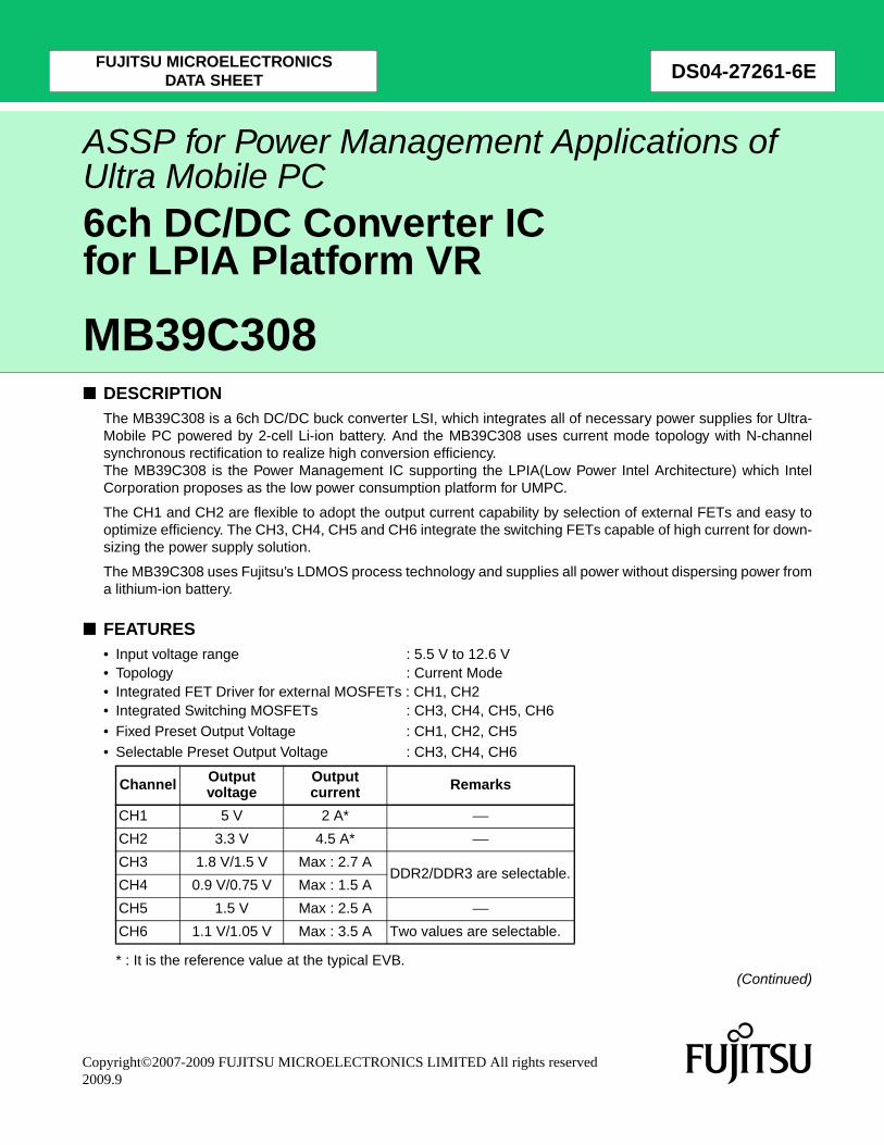
FUJITSU MICROELECTRONICSDATA SHEET DS04-27261-6E
ASSP for Power Management Applications of Ultra Mobile PC6ch DC/DC Converter IC for LPIA Platform VR
MB39C308■ DESCRIPTION
The MB39C308 is a 6ch DC/DC buck converter LSI, which integrates all of necessary power supplies for Ultra-Mobile PC powered by 2-cell Li-ion battery. And the MB39C308 uses current mode topology with N-channelsynchronous rectification to realize high conversion efficiency. The MB39C308 is the Power Management IC supporting the LPIA(Low Power Intel Architecture) which IntelCorporation proposes as the low power consumption platform for UMPC.
The CH1 and CH2 are flexible to adopt the output current capability by selection of external FETs and easy tooptimize efficiency. The CH3, CH4, CH5 and CH6 integrate the switching FETs capable of high current for down-sizing the power supply solution.
The MB39C308 uses Fujitsu’s LDMOS process technology and supplies all power without dispersing power froma lithium-ion battery.
■ FEATURES • Input voltage range : 5.5 V to 12.6 V• Topology : Current Mode• Integrated FET Driver for external MOSFETs : CH1, CH2• Integrated Switching MOSFETs : CH3, CH4, CH5, CH6• Fixed Preset Output Voltage : CH1, CH2, CH5• Selectable Preset Output Voltage : CH3, CH4, CH6
* : It is the reference value at the typical EVB.(Continued)
Channel Output voltage
Output current Remarks
CH1 5 V 2 A* ⎯CH2 3.3 V 4.5 A* ⎯CH3 1.8 V/1.5 V Max : 2.7 A
DDR2/DDR3 are selectable.CH4 0.9 V/0.75 V Max : 1.5 A
CH5 1.5 V Max : 2.5 A ⎯CH6 1.1 V/1.05 V Max : 3.5 A Two values are selectable.
Copyright©2007-2009 FUJITSU MICROELECTRONICS LIMITED All rights reserved2009.9
MB39C308
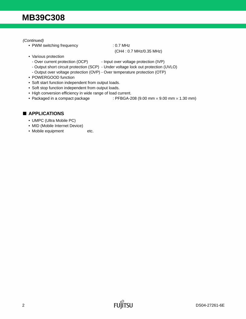
(Continued)• PWM switching frequency : 0.7 MHz
(CH4 : 0.7 MHz/0.35 MHz)• Various protection
- Over current protection (OCP) - Input over voltage protection (IVP)- Output short circuit protection (SCP) - Under voltage lock out protection (UVLO)- Output over voltage protection (OVP) - Over temperature protection (OTP)
• POWERGOOD function• Soft start function independent from output loads.• Soft stop function independent from output loads.• High conversion efficiency in wide range of load current.• Packaged in a compact package : PFBGA-208 (9.00 mm × 9.00 mm × 1.30 mm)
■ APPLICATIONS• UMPC (Ultra Mobile PC)• MID (Mobile Internet Device)• Mobile equipment etc.
2 DS04-27261-6E
MB39C308
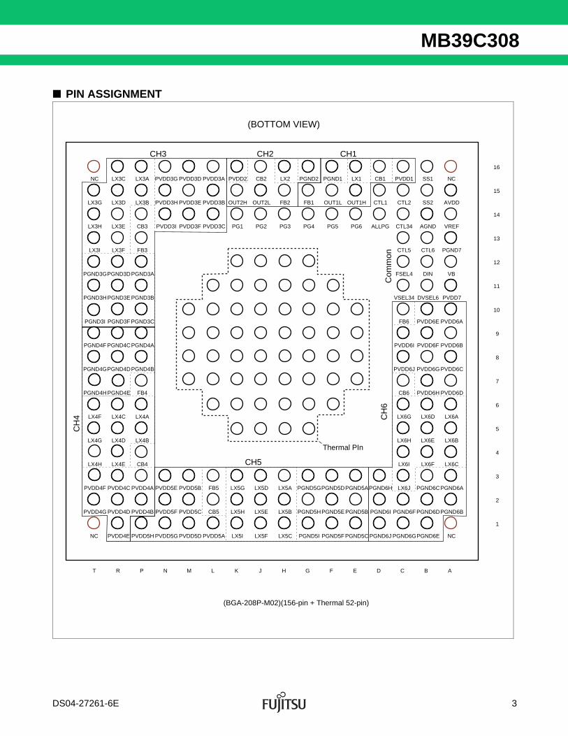
■ PIN ASSIGNMENT
Com
mon
CH3 CH2 CH1
16
15
14
13
12
11
10
9
8
7
6
5
4
3
2
1
NC LX3C LX3A PVDD3G PVDD3D PVDD3A PVDD2 CB2 LX2 PGND2 PGND1 LX1 CB1 PVDD1 SS1 NC
LX3G LX3D LX3B PVDD3H PVDD3E PVDD3B OUT2H OUT2L FB2 FB1 OUT1L OUT1H CTL1 CTL2 SS2 AVDD
LX3H LX3E CB3 PVDD3I PVDD3F PVDD3C PG1 PG2 PG3 PG4 PG5 PG6 ALLPG CTL34 AGND VREF
LX3I LX3F FB3 CTL5 CTL6 PGND7
PGND3GPGND3DPGND3A FSEL4 DIN VB
PGND3HPGND3E PGND3B VSEL34 DVSEL6 PVDD7
PGND3I PGND3F PGND3C FB6 PVDD6E PVDD6A
PGND4F PGND4CPGND4A PVDD6I PVDD6F PVDD6B
PGND4GPGND4DPGND4B PVDD6J PVDD6G PVDD6C
PGND4HPGND4E FB4 CB6 PVDD6H PVDD6D
CH5
CH
4 CH
6
LX4F LX4C LX4A LX6G LX6D LX6A
LX4G LX4D LX4B LX6H LX6E LX6B
LX4H LX4E CB4 LX6I LX6F LX6C
PVDD4F PVDD4C PVDD4A PVDD5E PVDD5B FB5 LX5G LX5D LX5A PGND5GPGND5DPGND5APGND6H LX6J PGND6CPGND6A
PVDD4G PVDD4D PVDD4B PVDD5F PVDD5C CB5 LX5H LX5E LX5B PGND5HPGND5E PGND5B PGND6I PGND6F PGND6DPGND6B
NC PVDD4E PVDD5H PVDD5G PVDD5D PVDD5A LX5I LX5F LX5C PGND5I PGND5F PGND5C PGND6J PGND6GPGND6E NC
T R P N M L K J H G F E D C B A
Thermal PIn
(BGA-208P-M02)(156-pin + Thermal 52-pin)
(BOTTOM VIEW)
DS04-27261-6E 3
MB39C308
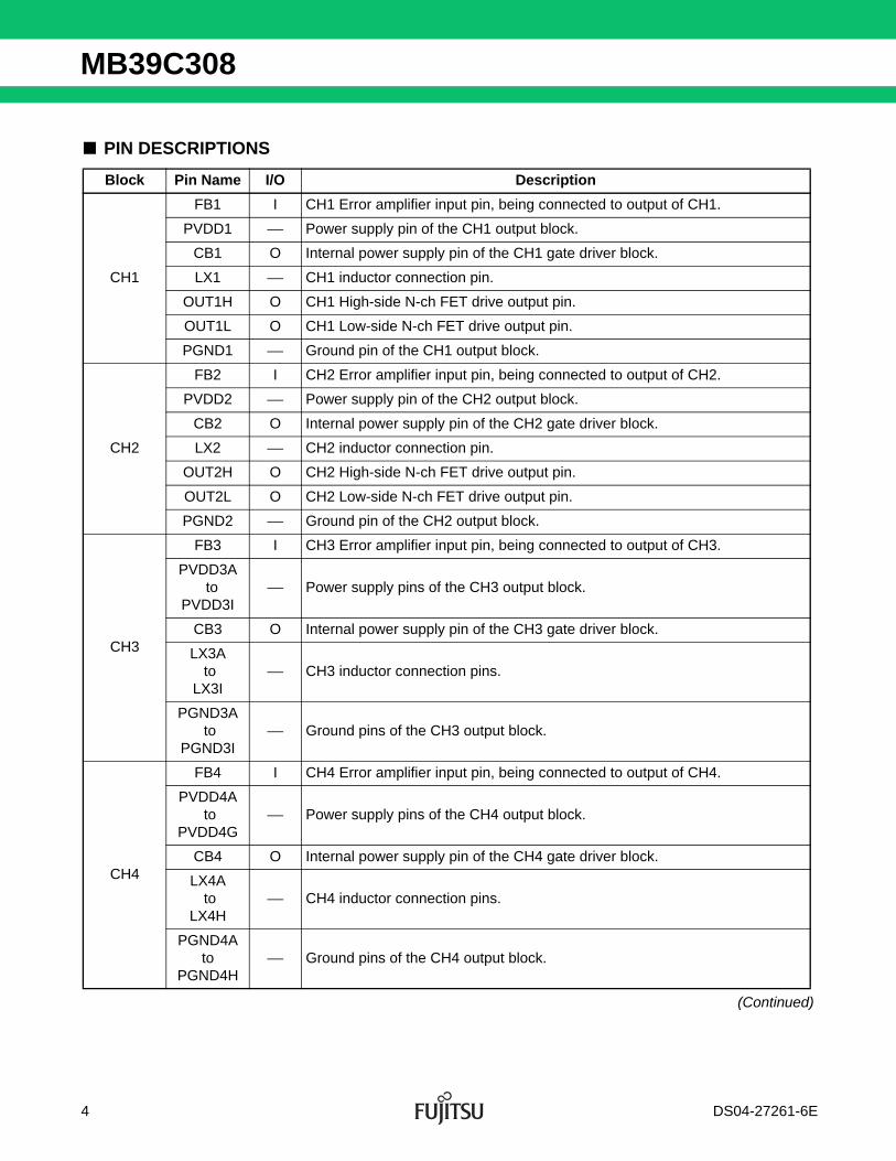
■ PIN DESCRIPTIONS
(Continued)
Block Pin Name I/O Description
CH1
FB1 I CH1 Error amplifier input pin, being connected to output of CH1.
PVDD1 ⎯ Power supply pin of the CH1 output block.
CB1 O Internal power supply pin of the CH1 gate driver block.
LX1 ⎯ CH1 inductor connection pin.
OUT1H O CH1 High-side N-ch FET drive output pin.
OUT1L O CH1 Low-side N-ch FET drive output pin.
PGND1 ⎯ Ground pin of the CH1 output block.
CH2
FB2 I CH2 Error amplifier input pin, being connected to output of CH2.
PVDD2 ⎯ Power supply pin of the CH2 output block.
CB2 O Internal power supply pin of the CH2 gate driver block.
LX2 ⎯ CH2 inductor connection pin.
OUT2H O CH2 High-side N-ch FET drive output pin.
OUT2L O CH2 Low-side N-ch FET drive output pin.
PGND2 ⎯ Ground pin of the CH2 output block.
CH3
FB3 I CH3 Error amplifier input pin, being connected to output of CH3.
PVDD3A to
PVDD3I⎯ Power supply pins of the CH3 output block.
CB3 O Internal power supply pin of the CH3 gate driver block.
LX3A to
LX3I⎯ CH3 inductor connection pins.
PGND3A to
PGND3I⎯ Ground pins of the CH3 output block.
CH4
FB4 I CH4 Error amplifier input pin, being connected to output of CH4.
PVDD4A to
PVDD4G⎯ Power supply pins of the CH4 output block.
CB4 O Internal power supply pin of the CH4 gate driver block.
LX4A to
LX4H⎯ CH4 inductor connection pins.
PGND4A to
PGND4H⎯ Ground pins of the CH4 output block.
4 DS04-27261-6E
MB39C308
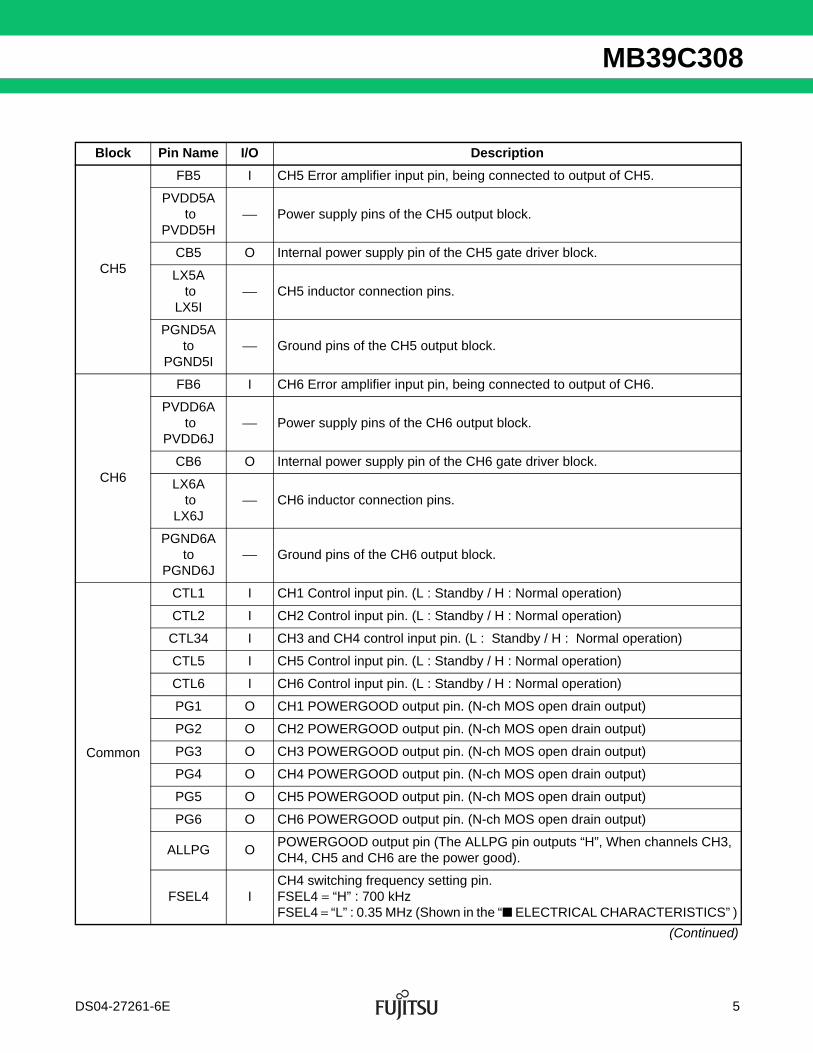
(Continued)
Block Pin Name I/O Description
CH5
FB5 I CH5 Error amplifier input pin, being connected to output of CH5.
PVDD5A to
PVDD5H⎯ Power supply pins of the CH5 output block.
CB5 O Internal power supply pin of the CH5 gate driver block.
LX5A to
LX5I⎯ CH5 inductor connection pins.
PGND5A to
PGND5I⎯ Ground pins of the CH5 output block.
CH6
FB6 I CH6 Error amplifier input pin, being connected to output of CH6.
PVDD6A to
PVDD6J⎯ Power supply pins of the CH6 output block.
CB6 O Internal power supply pin of the CH6 gate driver block.
LX6A to
LX6J⎯ CH6 inductor connection pins.
PGND6A to
PGND6J⎯ Ground pins of the CH6 output block.
Common
CTL1 I CH1 Control input pin. (L : Standby / H : Normal operation)
CTL2 I CH2 Control input pin. (L : Standby / H : Normal operation)
CTL34 I CH3 and CH4 control input pin. (L : Standby / H : Normal operation)
CTL5 I CH5 Control input pin. (L : Standby / H : Normal operation)
CTL6 I CH6 Control input pin. (L : Standby / H : Normal operation)
PG1 O CH1 POWERGOOD output pin. (N-ch MOS open drain output)
PG2 O CH2 POWERGOOD output pin. (N-ch MOS open drain output)
PG3 O CH3 POWERGOOD output pin. (N-ch MOS open drain output)
PG4 O CH4 POWERGOOD output pin. (N-ch MOS open drain output)
PG5 O CH5 POWERGOOD output pin. (N-ch MOS open drain output)
PG6 O CH6 POWERGOOD output pin. (N-ch MOS open drain output)
ALLPG OPOWERGOOD output pin (The ALLPG pin outputs “H”, When channels CH3, CH4, CH5 and CH6 are the power good).
FSEL4 ICH4 switching frequency setting pin.FSEL4 = “H” : 700 kHzFSEL4 = “L” : 0.35 MHz (Shown in the “■ ELECTRICAL CHARACTERISTICS” )
DS04-27261-6E 5
MB39C308
(Continued)
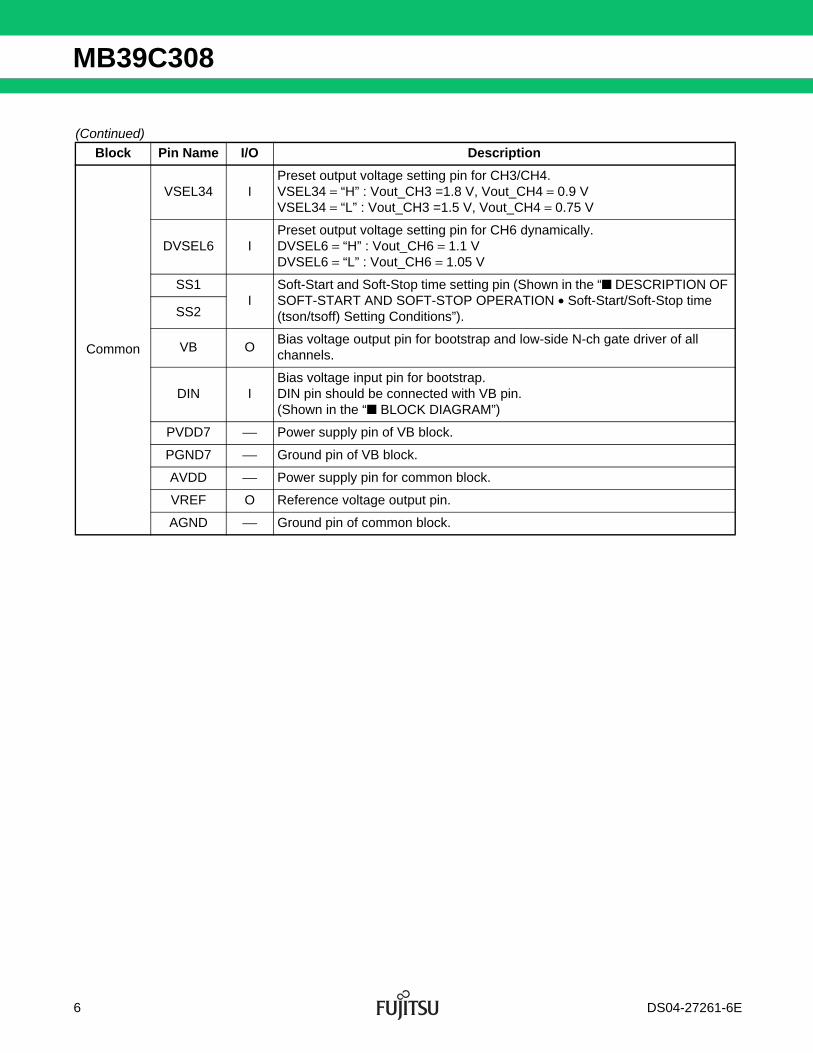
Block Pin Name I/O Description
Common
VSEL34 IPreset output voltage setting pin for CH3/CH4.VSEL34 = “H” : Vout_CH3 =1.8 V, Vout_CH4 = 0.9 VVSEL34 = “L” : Vout_CH3 =1.5 V, Vout_CH4 = 0.75 V
DVSEL6 IPreset output voltage setting pin for CH6 dynamically.DVSEL6 = “H” : Vout_CH6 = 1.1 VDVSEL6 = “L” : Vout_CH6 = 1.05 V
SS1I
Soft-Start and Soft-Stop time setting pin (Shown in the “■ DESCRIPTION OF SOFT-START AND SOFT-STOP OPERATION • Soft-Start/Soft-Stop time (tson/tsoff) Setting Conditions”).SS2
VB OBias voltage output pin for bootstrap and low-side N-ch gate driver of all channels.
DIN IBias voltage input pin for bootstrap.DIN pin should be connected with VB pin.(Shown in the “■ BLOCK DIAGRAM”)
PVDD7 ⎯ Power supply pin of VB block.
PGND7 ⎯ Ground pin of VB block.
AVDD ⎯ Power supply pin for common block.
VREF O Reference voltage output pin.
AGND ⎯ Ground pin of common block.
6 DS04-27261-6E
MB39C308
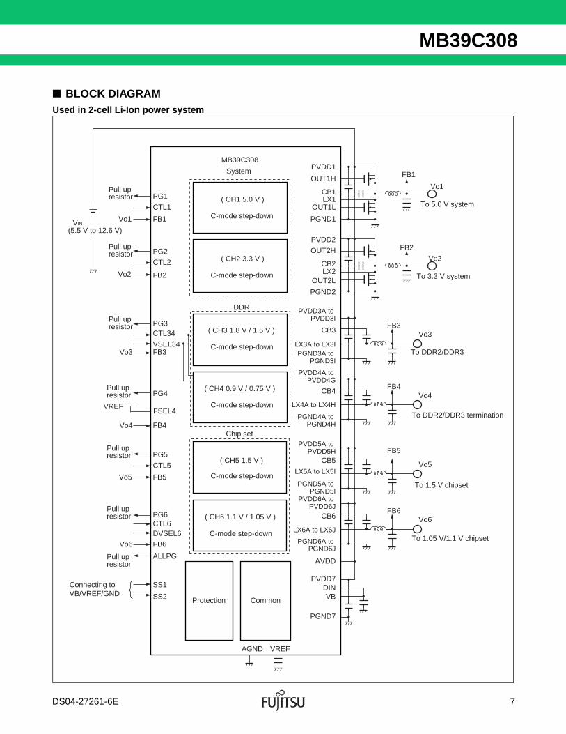
■ BLOCK DIAGRAMUsed in 2-cell Li-Ion power system
To 5.0 V system
FB1
Vo1
To 3.3 V system
Vo2
FB2
To DDR2/DDR3
Vo3FB3
To DDR2/DDR3 termination
Vo4FB4
To 1.5 V chipset
Vo5
FB5
To 1.05 V/1.1 V chipset
Vo6FB6
CommonProtection
AGND VREF
CB6
LX6A to LX6J
PVDD6A to PVDD6J
PGND6A to PGND6J
VBDIN
AVDD
PGND7
PVDD7
( CH6 1.1 V / 1.05 V )
C-mode step-down
C-mode step-down
C-mode step-down
( CH5 1.5 V )
( CH4 0.9 V / 0.75 V )
C-mode step-down
( CH3 1.8 V / 1.5 V )
C-mode step-down
( CH2 3.3 V )
C-mode step-down
( CH1 5.0 V )
Chip set
CB5
LX5A to LX5I
PVDD5A to PVDD5H
PGND5A to PGND5I
CB4
LX4A to LX4H
PVDD4A to PVDD4G
PGND4A to PGND4H
CB3
LX3A to LX3I
PVDD3A to PVDD3I
PGND3A to PGND3I
DDR
OUT2H
CB2LX2
PVDD2
PGND2
OUT2L
MB39C308
SystemOUT1H
PVDD1
PGND1
OUT1L
CB1LX1
CTL1
FB1
PG1Pull upresistor
Pull upresistor
Pull upresistor
Pull upresistor
Pull upresistor
Pull upresistor
Pull upresistor
Vo1
Vo2
CTL2
FB2
PG2
Vo3
CTL34
VSEL34FB3
PG3
Vo4
VREFFSEL4
CTL5
Vo5 FB5
FB4
PG4
PG5
CTL6
Vo6 FB6
DVSEL6
PG6
ALLPG
SS1
SS2
Connecting toVB/VREF/GND
(5.5 V to 12.6 V)VIN
DS04-27261-6E 7
MB39C308
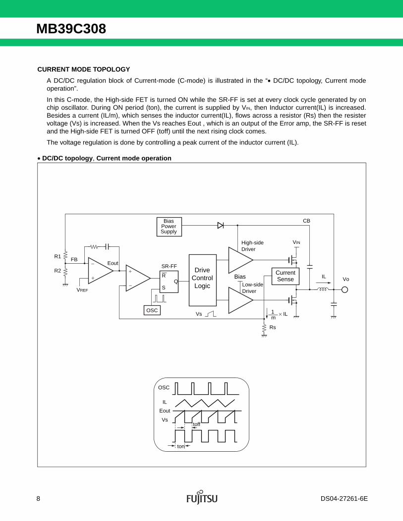
CURRENT MODE TOPOLOGY
A DC/DC regulation block of Current-mode (C-mode) is illustrated in the “• DC/DC topology, Current modeoperation”.
In this C-mode, the High-side FET is turned ON while the SR-FF is set at every clock cycle generated by onchip oscillator. During ON period (ton), the current is supplied by VIN, then Inductor current(IL) is increased.Besides a current (IL/m), which senses the inductor current(IL), flows across a resistor (Rs) then the resistervoltage (Vs) is increased. When the Vs reaches Eout , which is an output of the Error amp, the SR-FF is resetand the High-side FET is turned OFF (toff) until the next rising clock comes.
The voltage regulation is done by controlling a peak current of the inductor current (IL).
• DC/DC topology, Current mode operation
VREF
R1
R2
FBEout
OSC
VIN
IL
SR-FF
R
SQ
m× IL1
Rs
Vo
Vs
CB
ton
toff
OSC
IL
Eout
Vs
Bias Power Supply
Drive Control Logic
High-side Driver
Current Sense
Low-side Driver
Bias
8 DS04-27261-6E
MB39C308
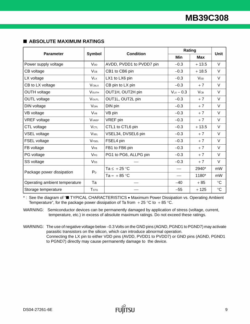
■ ABSOLUTE MAXIMUM RATINGS
* : See the diagram of “■ TYPICAL CHARACTERISTICS • Maximum Power Dissipation vs. Operating Ambient Temperature”, for the package power dissipation of Ta from + 25 °C to + 85 °C.
WARNING: Semiconductor devices can be permanently damaged by application of stress (voltage, current, temperature, etc.) in excess of absolute maximum ratings. Do not exceed these ratings.
WARNING: The use of negative voltage below −0.3 Volts on the GND pins (AGND, PGND1 to PGND7) may activate parasitic transistors on the silicon, which can introduce abnormal operation.Connecting the LX pin to either VDD pins (AVDD, PVDD1 to PVDD7) or GND pins (AGND, PGND1 to PGND7) directly may cause permanently damage to the device.
Parameter Symbol ConditionRating
UnitMin Max
Power supply voltage VDD AVDD, PVDD1 to PVDD7 pin −0.3 + 13.5 V
CB voltage VCB CB1 to CB6 pin −0.3 + 18.5 V
LX voltage VLX LX1 to LX6 pin −0.3 VDD V
CB to LX voltage VCBLX CB pin to LX pin −0.3 + 7 V
OUTH voltage VOUTH OUT1H, OUT2H pin VLX − 0.3 VCB V
OUTL voltage VOUTL OUT1L, OUT2L pin −0.3 + 7 V
DIN voltage VDIN DIN pin −0.3 + 7 V
VB voltage VVB VB pin −0.3 + 7 V
VREF voltage VVREF VREF pin −0.3 + 7 V
CTL voltage VCTL CTL1 to CTL6 pin −0.3 + 13.5 V
VSEL voltage VSEL VSEL34, DVSEL6 pin −0.3 + 7 V
FSEL voltage VFSEL FSEL4 pin −0.3 + 7 V
FB voltage VFB FB1 to FB6 pin −0.3 + 7 V
PG voltage VPG PG1 to PG6, ALLPG pin −0.3 + 7 V
SS voltage VSS ⎯ −0.3 + 7 V
Package power dissipation PDTa ≤ + 25 °C ⎯ 2940* mW
Ta = + 85 °C ⎯ 1180* mW
Operating ambient temperature Ta ⎯ −40 + 85 °C
Storage temperature TSTG ⎯ −55 + 125 °C
DS04-27261-6E 9
MB39C308
■ RECOMMENDED OPERATING CONDITIONS
(Continued)
Parameter Symbol ConditionValue
UnitMin Typ Max
Power supply voltage VDD AVDD = PVDD1 to PVDD7 pin 5.5 ⎯ 12.6 V
Input capacitor CIN VDD to GND pin ⎯ 4.7 ⎯ μF
CB to LX capacitor CCB CB to LX pin ⎯ 0.1 ⎯ μF
LX inductor
L1 LX1 pin ⎯ 3.3 ⎯ μH
L2 LX2 pin ⎯ 3.3 ⎯ μH
L3 LX3 pin ⎯ 1.5 ⎯ μH
L4
LX4 pin, FSEL4 pin = H fosc = 0.7 MHz
⎯ 1.5 ⎯μH
LX4 pin, FSEL4 pin = L fosc = 0.35 MHz
⎯ 1.5 ⎯
L5 LX5 pin ⎯ 1.5 ⎯ μH
L6 LX6 pin ⎯ 1.5 ⎯ μH
Output current
IO1 Vo1 (5 V), DC, when RonH1 = 32 mΩ ⎯ 1 2* A
IO2 Vo2 (3.3 V), DC, when RonH2 = 16 mΩ ⎯ 2.25 4.5* A
IO3 Vo3 (1.8 V/1.5 V), DC ⎯ 1.35 2.7* A
IO4 Vo4 (0.9 V/0.75 V), DC ⎯ 1 1.5* A
IO5 Vo5 (1.5 V), DC ⎯ 1.25 2.5* A
IO6 Vo6 (1.1 V/1.05 V), DC ⎯ 1.75 3.5* A
Output capacitor
CO1Vo1 (5 V), when RonH1 = 32 mΩ, L = 3.3 μH, SS1,SS2 pin = GND
⎯ 100 300 μF
CO2Vo2 (3.3 V), when RonH1 = 16 mΩ, L = 3.3 μH, SS1,SS2 pin = GND
⎯ 100 700 μF
CO3Vo3 (1.8 V), when L = 1.5 μH, SS1, SS2 pin = GND
⎯ 100 300 μF
CO4Vo4 (0.9 V), when L = 1.5 μH, SS1, SS2 pin = GND
⎯ 100 500 μF
CO5Vo5 (1.5 V), when L = 1.5 μH, SS1, SS2 pin = GND
⎯ 100 300 μF
CO6Vo6 (1.05 V), when L = 1.5 μH, SS1, SS2 pin = GND
⎯ 200 500 μF
External FET On-resistance
RonH1CH1 High-side FET connected to OUT1H pin
⎯ 32 ⎯ mΩ
RonL1CH1 Low-side FET connected to OUT1L pin
⎯ 32 ⎯ mΩ
RonH2CH2 High-side FET connected to OUT2H pin
12 16 20 mΩ
RonL2CH2 Low-side FET connected to OUT2L pin
⎯ 16 ⎯ mΩ
10 DS04-27261-6E
MB39C308
(Continued)
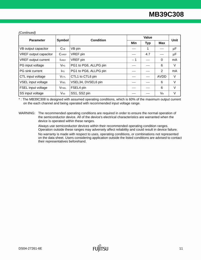
* : The MB39C308 is designed with assumed operating conditions, which is 60% of the maximum output current on the each channel and being operated with recommended input voltage range.
WARNING: The recommended operating conditions are required in order to ensure the normal operation of the semiconductor device. All of the device's electrical characteristics are warranted when the device is operated within these ranges.
Always use semiconductor devices within their recommended operating condition ranges. Operation outside these ranges may adversely affect reliability and could result in device failure.No warranty is made with respect to uses, operating conditions, or combinations not represented on the data sheet. Users considering application outside the listed conditions are advised to contact their representatives beforehand.
Parameter Symbol ConditionValue
UnitMin Typ Max
VB output capacitor CVB VB pin ⎯ 1 ⎯ μF
VREF output capacitor CVREF VREF pin ⎯ 4.7 ⎯ μF
VREF output current IVREF VREF pin − 1 ⎯ 0 mA
PG input voltage VPG PG1 to PG6, ALLPG pin ⎯ ⎯ 6 V
PG sink current IPG PG1 to PG6, ALLPG pin ⎯ ⎯ 2 mA
CTL input voltage VCTL CTL1 to CTL6 pin ⎯ ⎯ AVDD V
VSEL input voltage VSEL VSEL34, DVSEL6 pin ⎯ ⎯ 6 V
FSEL input voltage VFSEL FSEL4 pin ⎯ ⎯ 6 V
SS input voltage VSS SS1, SS2 pin ⎯ ⎯ VB V
DS04-27261-6E 11
MB39C308
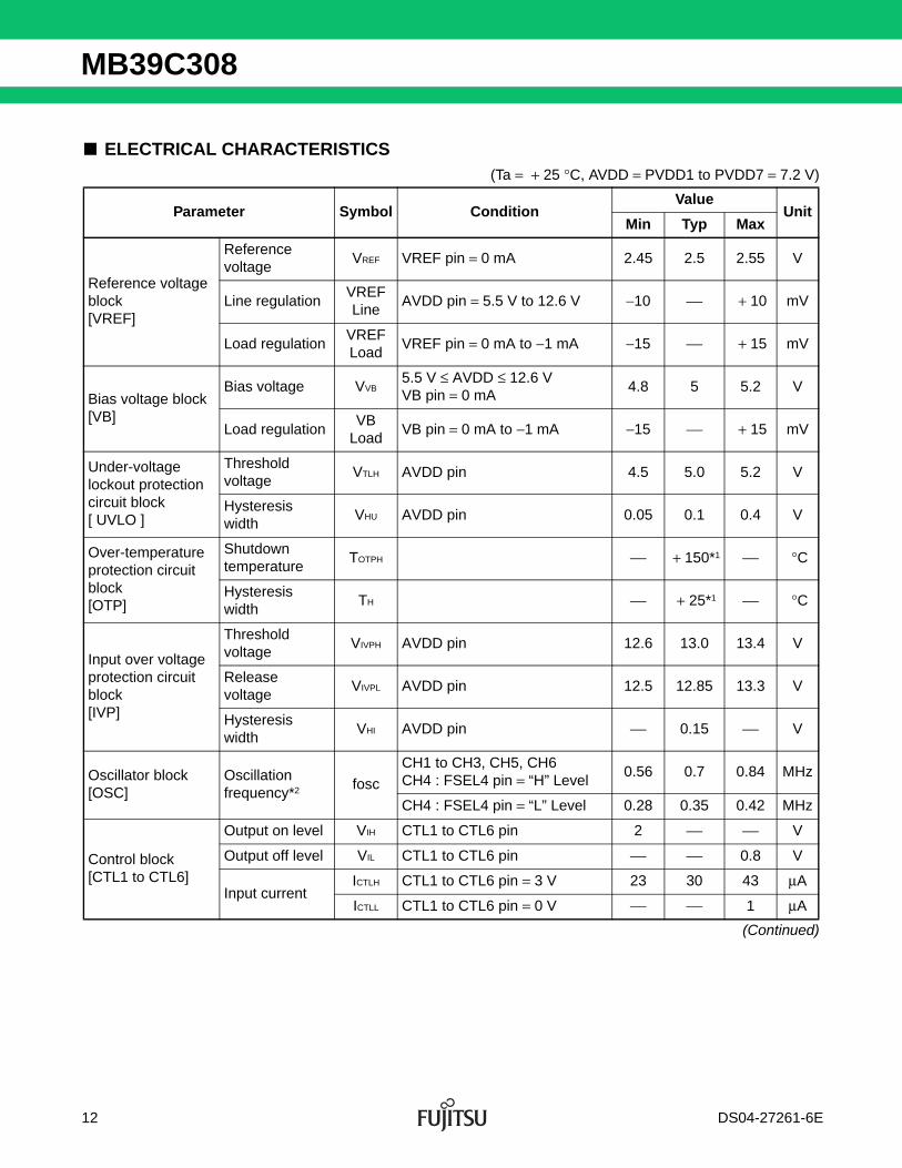
■ ELECTRICAL CHARACTERISTICS(Ta = + 25 °C, AVDD = PVDD1 to PVDD7 = 7.2 V)
(Continued)
Parameter Symbol ConditionValue
UnitMin Typ Max
Reference voltage block[VREF]
Reference voltage
VREF VREF pin = 0 mA 2.45 2.5 2.55 V
Line regulationVREFLine
AVDD pin = 5.5 V to 12.6 V −10 ⎯ + 10 mV
Load regulationVREFLoad
VREF pin = 0 mA to −1 mA −15 ⎯ + 15 mV
Bias voltage block[VB]
Bias voltage VVB5.5 V ≤ AVDD ≤ 12.6 VVB pin = 0 mA
4.8 5 5.2 V
Load regulationVB
LoadVB pin = 0 mA to −1 mA −15 ⎯ + 15 mV
Under-voltage lockout protection circuit block[ UVLO ]
Threshold voltage
VTLH AVDD pin 4.5 5.0 5.2 V
Hysteresis width
VHU AVDD pin 0.05 0.1 0.4 V
Over-temperature protection circuit block [OTP]
Shutdown temperature
TOTPH ⎯ + 150*1 ⎯ °C
Hysteresis width
TH ⎯ + 25*1 ⎯ °C
Input over voltage protection circuit block [IVP]
Threshold voltage
VIVPH AVDD pin 12.6 13.0 13.4 V
Release voltage
VIVPL AVDD pin 12.5 12.85 13.3 V
Hysteresis width
VHI AVDD pin ⎯ 0.15 ⎯ V
Oscillator block [OSC]
Oscillation frequency*2 fosc
CH1 to CH3, CH5, CH6CH4 : FSEL4 pin = “H” Level
0.56 0.7 0.84 MHz
CH4 : FSEL4 pin = “L” Level 0.28 0.35 0.42 MHz
Control block [CTL1 to CTL6]
Output on level VIH CTL1 to CTL6 pin 2 ⎯ ⎯ V
Output off level VIL CTL1 to CTL6 pin ⎯ ⎯ 0.8 V
Input currentICTLH CTL1 to CTL6 pin = 3 V 23 30 43 μA
ICTLL CTL1 to CTL6 pin = 0 V ⎯ ⎯ 1 μA
12 DS04-27261-6E
MB39C308
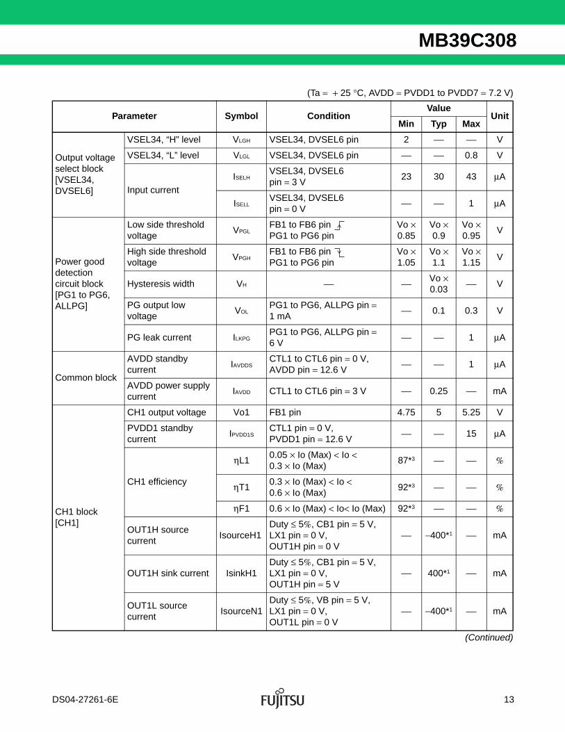
(Ta = + 25 °C, AVDD = PVDD1 to PVDD7 = 7.2 V)
(Continued)
Parameter Symbol ConditionValue
UnitMin Typ Max
Output voltage select block [VSEL34, DVSEL6]
VSEL34, “H” level VLGH VSEL34, DVSEL6 pin 2 ⎯ ⎯ V
VSEL34, “L” level VLGL VSEL34, DVSEL6 pin ⎯ ⎯ 0.8 V
Input current
ISELHVSEL34, DVSEL6 pin = 3 V
23 30 43 μA
ISELLVSEL34, DVSEL6 pin = 0 V
⎯ ⎯ 1 μA
Power gooddetection circuit block[PG1 to PG6, ALLPG]
Low side threshold voltage
VPGLFB1 to FB6 pin PG1 to PG6 pin
Vo × 0.85
Vo × 0.9
Vo × 0.95
V
High side threshold voltage
VPGHFB1 to FB6 pin PG1 to PG6 pin
Vo × 1.05
Vo × 1.1
Vo × 1.15
V
Hysteresis width VH ⎯ ⎯ Vo × 0.03
⎯ V
PG output low voltage
VOLPG1 to PG6, ALLPG pin = 1 mA
⎯ 0.1 0.3 V
PG leak current ILKPGPG1 to PG6, ALLPG pin = 6 V
⎯ ⎯ 1 μA
Common block
AVDD standby current
IAVDDSCTL1 to CTL6 pin = 0 V, AVDD pin = 12.6 V
⎯ ⎯ 1 μA
AVDD power supply current
IAVDD CTL1 to CTL6 pin = 3 V ⎯ 0.25 ⎯ mA
CH1 block[CH1]
CH1 output voltage Vo1 FB1 pin 4.75 5 5.25 V
PVDD1 standby current
IPVDD1SCTL1 pin = 0 V, PVDD1 pin = 12.6 V
⎯ ⎯ 15 μA
CH1 efficiency
ηL10.05 × Io (Max) < Io < 0.3 × Io (Max)
87*3 ⎯ ⎯ %
ηT10.3 × Io (Max) < Io < 0.6 × Io (Max)
92*3 ⎯ ⎯ %
ηF1 0.6 × Io (Max) < Io< Io (Max) 92*3 ⎯ ⎯ %
OUT1H source current
IsourceH1Duty ≤ 5%, CB1 pin = 5 V, LX1 pin = 0 V, OUT1H pin = 0 V
⎯ −400*1 ⎯ mA
OUT1H sink current IsinkH1Duty ≤ 5%, CB1 pin = 5 V, LX1 pin = 0 V, OUT1H pin = 5 V
⎯ 400*1 ⎯ mA
OUT1L source current
IsourceN1Duty ≤ 5%, VB pin = 5 V, LX1 pin = 0 V, OUT1L pin = 0 V
⎯ −400*1 ⎯ mA
DS04-27261-6E 13
MB39C308
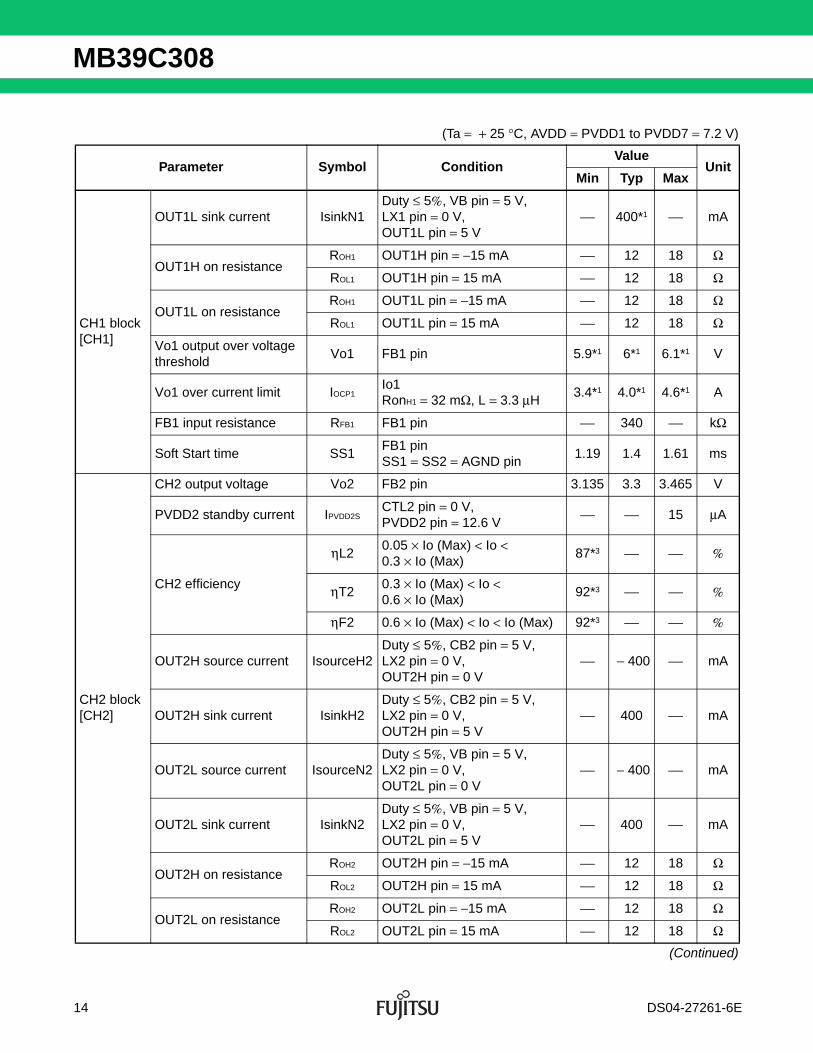
(Ta = + 25 °C, AVDD = PVDD1 to PVDD7 = 7.2 V)
(Continued)
Parameter Symbol ConditionValue
UnitMin Typ Max
CH1 block [CH1]
OUT1L sink current IsinkN1Duty ≤ 5%, VB pin = 5 V, LX1 pin = 0 V, OUT1L pin = 5 V
⎯ 400*1 ⎯ mA
OUT1H on resistanceROH1 OUT1H pin = −15 mA ⎯ 12 18 Ω
ROL1 OUT1H pin = 15 mA ⎯ 12 18 Ω
OUT1L on resistanceROH1 OUT1L pin = −15 mA ⎯ 12 18 Ω
ROL1 OUT1L pin = 15 mA ⎯ 12 18 Ω
Vo1 output over voltage threshold
Vo1 FB1 pin 5.9*1 6*1 6.1*1 V
Vo1 over current limit IOCP1Io1RonH1 = 32 mΩ, L = 3.3 μH
3.4*1 4.0*1 4.6*1 A
FB1 input resistance RFB1 FB1 pin ⎯ 340 ⎯ kΩ
Soft Start time SS1FB1 pinSS1 = SS2 = AGND pin
1.19 1.4 1.61 ms
CH2 block [CH2]
CH2 output voltage Vo2 FB2 pin 3.135 3.3 3.465 V
PVDD2 standby current IPVDD2SCTL2 pin = 0 V, PVDD2 pin = 12.6 V
⎯ ⎯ 15 μA
CH2 efficiency
ηL20.05 × Io (Max) < Io < 0.3 × Io (Max)
87*3 ⎯ ⎯ %
ηT20.3 × Io (Max) < Io < 0.6 × Io (Max)
92*3 ⎯ ⎯ %
ηF2 0.6 × Io (Max) < Io < Io (Max) 92*3 ⎯ ⎯ %
OUT2H source current IsourceH2Duty ≤ 5%, CB2 pin = 5 V, LX2 pin = 0 V, OUT2H pin = 0 V
⎯ − 400 ⎯ mA
OUT2H sink current IsinkH2Duty ≤ 5%, CB2 pin = 5 V, LX2 pin = 0 V, OUT2H pin = 5 V
⎯ 400 ⎯ mA
OUT2L source current IsourceN2Duty ≤ 5%, VB pin = 5 V, LX2 pin = 0 V, OUT2L pin = 0 V
⎯ − 400 ⎯ mA
OUT2L sink current IsinkN2Duty ≤ 5%, VB pin = 5 V, LX2 pin = 0 V, OUT2L pin = 5 V
⎯ 400 ⎯ mA
OUT2H on resistanceROH2 OUT2H pin = −15 mA ⎯ 12 18 Ω
ROL2 OUT2H pin = 15 mA ⎯ 12 18 Ω
OUT2L on resistanceROH2 OUT2L pin = −15 mA ⎯ 12 18 Ω
ROL2 OUT2L pin = 15 mA ⎯ 12 18 Ω
14 DS04-27261-6E
MB39C308
(Ta = + 25 °C, AVDD = PVDD1 to PVDD7 = 7.2 V)
(Continued)
Parameter Symbol ConditionValue
UnitMin Typ Max
CH2 block [CH2]
Vo2 output over voltage threshold
Vo2 FB2 pin 3.894*1 3.96*1 4.026*1 V
Vo2 over current limit IOCP2IO2RonH1 = 16 mΩ, L = 3.3 μH
6.7*1 7.9*1 9.0*1 A
FB2 input resistance RFB2 FB2 pin ⎯ 220 ⎯ kΩ
Soft start time SS2FB2 pinSS1 = SS2 = AGND pin
1.19 1.4 1.61 ms
CH3 block [CH3]
CH3 output voltage Vo3
VSEL34 = “H” Level, FB3 pin
1.71 1.8 1.89 V
VSEL34 = “L” Level, FB3 pin
1.425 1.5 1.575 V
High-side FET on-resistance
RONH3LX3 pin = −100 mA, VGS = 5 V
⎯ 65*1 ⎯ mΩ
Low-side FET on-resistance
RONL3LX3 pin = 100 mA, VGS = 5 V
⎯ 40*1 ⎯ mΩ
PVDD3 standby current IPVDD3SCTL34 pin = 0 V, PVDD3 pin = 12.6 V
⎯ ⎯ 15 μA
CH3 efficiency
ηL31
VSEL34 pin = “H” Level, Vo3 = 1.8 V0.05 × Io (Max) < Io < 0.3 × Io (Max)
85*3 ⎯ ⎯ %
ηL32
VSEL34 pin = “L” Level, Vo3 = 1.5 V0.05 × Io (Max) < Io <0.3 × Io (Max)
82*3 ⎯ ⎯ %
ηT31
VSEL34 pin = “H” Level, Vo3 = 1.8 V0.3 × Io (Max) < Io < 0.6 × Io (Max)
87*3 ⎯ ⎯ %
ηT32
VSEL34 pin = “L” Level, Vo3 = 1.5 V0.3 × Io (Max) < Io < 0.6 × Io (Max)
85*3 ⎯ ⎯ %
ηF31
VSEL34 pin = “H” Level, Vo3 = 1.8 V0.6 × Io (Max) < Io < Io (Max)
87*3 ⎯ ⎯ %
ηF32
VSEL34 pin = “L” Level, Vo3 = 1.5 V0.6 × Io (Max) < Io < Io (Max)
85*3 ⎯ ⎯ %
DS04-27261-6E 15
MB39C308
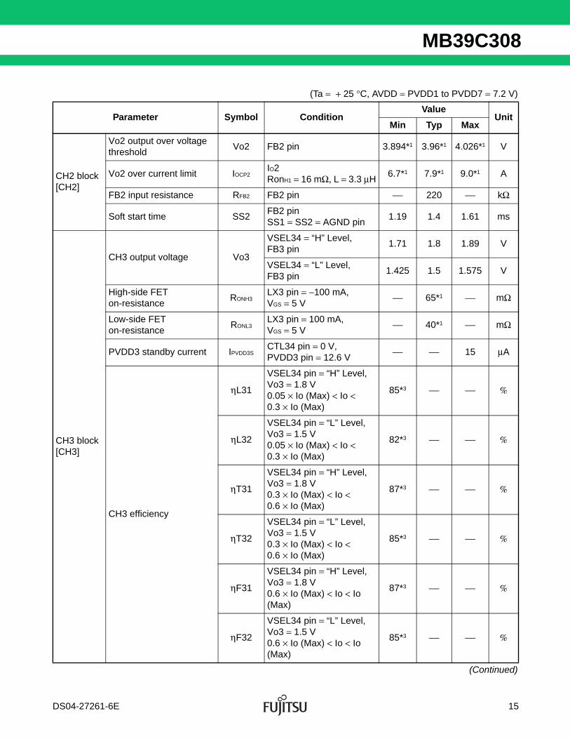
(Ta = + 25 °C, AVDD = PVDD1 to PVDD7 = 7.2 V)
(Continued)
Parameter Symbol ConditionValue
UnitMin Typ Max
CH3 block [CH3]
Vo3 output over voltage threshold
VOVP3
VSEL34 pin = “H” Level, Vo3 = 1.8 V, FB3 pin
2.124*1 2.16*1 2.196*1 V
VSEL34 pin = “L” Level,Vo3 = 1.5 V, FB3 pin
1.77*1 1.8*1 1.83*1 V
Vo3 over current limit IOCP3Io3, L = 1.5 μH
3.0*1 3.75*1 4.5*1 A
FB3 input resistance RFB3 FB3 pin ⎯ 250 ⎯ kΩ
Soft start time SS3FB3 pinSS1 = SS2 = AGND pin
1.19 1.4 1.61 ms
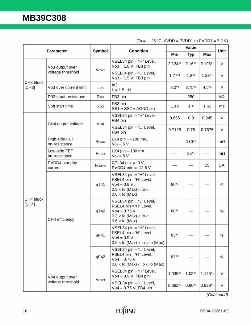
CH4 block [CH4]
CH4 output voltage Vo4
VSEL34 pin = “H” Level, FB4 pin
0.855 0.9 0.945 V
VSEL34 pin = “L” Level, FB4 pin
0.7125 0.75 0.7875 V
High-side FET on-resistance
RONH4LX4 pin = −100 mA, VGS = 5 V
⎯ 130*1 ⎯ mΩ
Low-side FET on-resistance
RONL4LX4 pin = 100 mA, VGS = 5 V
⎯ 55*1 ⎯ mΩ
PVDD4 standby current
IPVDD4SCTL34 pin = 0 V, PVDD4 pin = 12.6 V
⎯ ⎯ 15 μA
CH4 efficiency
ηT41
VSEL34 pin = “H” Level, FSEL4 pin =“H” Level,Vo4 = 0.9 V0.3 × Io (Max) < Io < 0.6 × Io (Max)
80*3 ⎯ ⎯ %
ηT42
VSEL34 pin = “L” Level, FSEL4 pin =“H” Level,Vo4 = 0.75 V0.3 × Io (Max) < Io <0.6 × Io (Max)
80*3 ⎯ ⎯ %
ηF41
VSEL34 pin = “H” Level, FSEL4 pin =“H” Level,Vo4 = 0.9 V0.6 × Io (Max) < Io < Io (Max)
83*3 ⎯ ⎯ %
ηF42
VSEL34 pin = “L” Level, FSEL4 pin =“H” Level,Vo4 = 0.75 V0.6 × Io (Max) < Io < Io (Max)
83*3 ⎯ ⎯ %
Vo4 output over voltage threshold
VOVP4
VSEL34 pin = “H” Level, Vo4 = 0.9 V, FB4 pin
1.035*1 1.08*1 1.125*1 V
VSEL34 pin = “L” Level, Vo4 = 0.75 V, FB4 pin
0.862*1 0.90*1 0.938*1 V
16 DS04-27261-6E
MB39C308
(Ta = + 25 °C, AVDD = PVDD1 to PVDD7 = 7.2 V)
(Continued)
Parameter Symbol ConditionValue
UnitMin Typ Max
CH4 block [CH4]
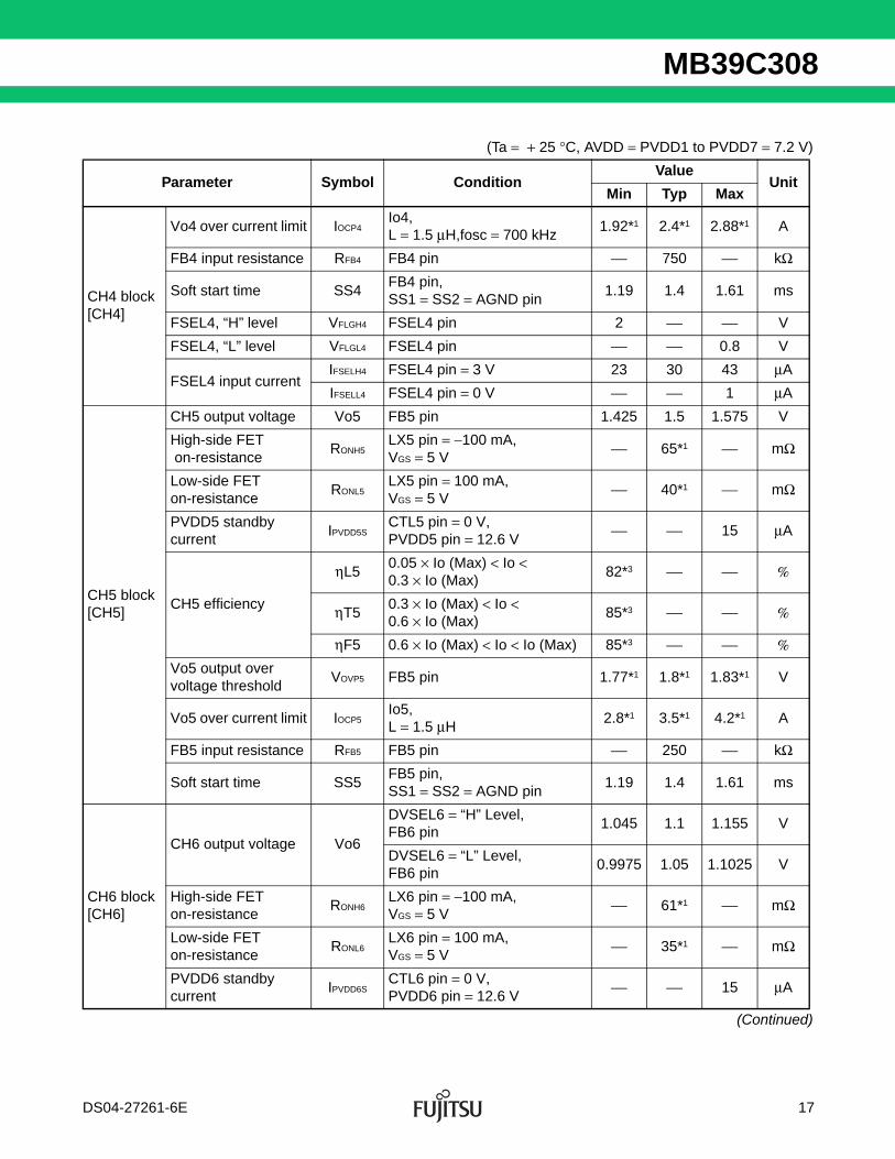
Vo4 over current limit IOCP4Io4,L = 1.5 μH,fosc = 700 kHz
1.92*1 2.4*1 2.88*1 A
FB4 input resistance RFB4 FB4 pin ⎯ 750 ⎯ kΩ
Soft start time SS4FB4 pin, SS1 = SS2 = AGND pin
1.19 1.4 1.61 ms
FSEL4, “H” level VFLGH4 FSEL4 pin 2 ⎯ ⎯ V
FSEL4, “L” level VFLGL4 FSEL4 pin ⎯ ⎯ 0.8 V
FSEL4 input currentIFSELH4 FSEL4 pin = 3 V 23 30 43 μA
IFSELL4 FSEL4 pin = 0 V ⎯ ⎯ 1 μA
CH5 block [CH5]
CH5 output voltage Vo5 FB5 pin 1.425 1.5 1.575 V
High-side FET on-resistance
RONH5LX5 pin = −100 mA, VGS = 5 V
⎯ 65*1 ⎯ mΩ
Low-side FET on-resistance
RONL5LX5 pin = 100 mA, VGS = 5 V
⎯ 40*1 ⎯ mΩ
PVDD5 standby current
IPVDD5SCTL5 pin = 0 V, PVDD5 pin = 12.6 V
⎯ ⎯ 15 μA
CH5 efficiency
ηL50.05 × Io (Max) < Io < 0.3 × Io (Max)
82*3 ⎯ ⎯ %
ηT50.3 × Io (Max) < Io < 0.6 × Io (Max)
85*3 ⎯ ⎯ %
ηF5 0.6 × Io (Max) < Io < Io (Max) 85*3 ⎯ ⎯ %Vo5 output over voltage threshold
VOVP5 FB5 pin 1.77*1 1.8*1 1.83*1 V
Vo5 over current limit IOCP5Io5, L = 1.5 μH
2.8*1 3.5*1 4.2*1 A
FB5 input resistance RFB5 FB5 pin ⎯ 250 ⎯ kΩ
Soft start time SS5FB5 pin, SS1 = SS2 = AGND pin
1.19 1.4 1.61 ms
CH6 block [CH6]
CH6 output voltage Vo6
DVSEL6 = “H” Level, FB6 pin
1.045 1.1 1.155 V
DVSEL6 = “L” Level, FB6 pin
0.9975 1.05 1.1025 V
High-side FET on-resistance
RONH6LX6 pin = −100 mA, VGS = 5 V
⎯ 61*1 ⎯ mΩ
Low-side FET on-resistance
RONL6LX6 pin = 100 mA, VGS = 5 V
⎯ 35*1 ⎯ mΩ
PVDD6 standby current
IPVDD6SCTL6 pin = 0 V, PVDD6 pin = 12.6 V
⎯ ⎯ 15 μA
DS04-27261-6E 17
MB39C308
(Continued)(Ta = + 25 °C, AVDD = PVDD1 to PVDD7 = 7.2 V)
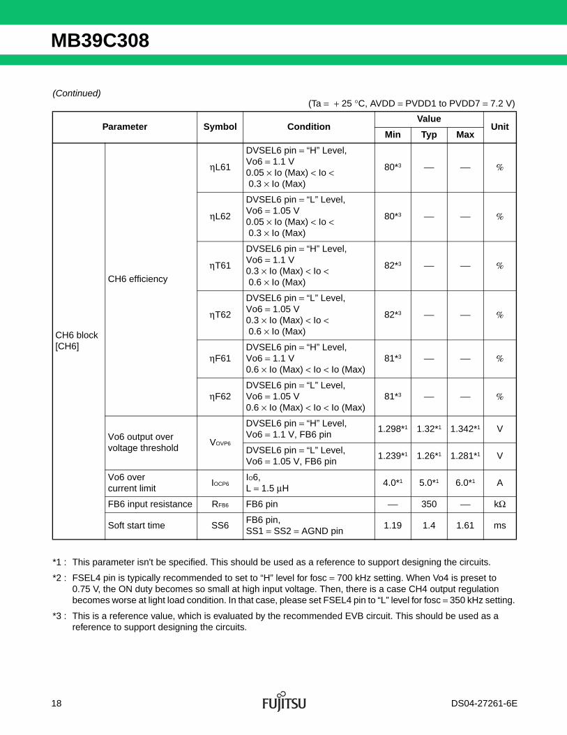
*1 : This parameter isn't be specified. This should be used as a reference to support designing the circuits.
*2 : FSEL4 pin is typically recommended to set to “H” level for fosc = 700 kHz setting. When Vo4 is preset to 0.75 V, the ON duty becomes so small at high input voltage. Then, there is a case CH4 output regulation becomes worse at light load condition. In that case, please set FSEL4 pin to “L” level for fosc = 350 kHz setting.
*3 : This is a reference value, which is evaluated by the recommended EVB circuit. This should be used as a reference to support designing the circuits.
Parameter Symbol ConditionValue
UnitMin Typ Max
CH6 block [CH6]
CH6 efficiency
ηL61
DVSEL6 pin = “H” Level, Vo6 = 1.1 V0.05 × Io (Max) < Io < 0.3 × Io (Max)
80*3 ⎯ ⎯ %
ηL62
DVSEL6 pin = “L” Level, Vo6 = 1.05 V0.05 × Io (Max) < Io < 0.3 × Io (Max)
80*3 ⎯ ⎯ %
ηT61
DVSEL6 pin = “H” Level, Vo6 = 1.1 V0.3 × Io (Max) < Io < 0.6 × Io (Max)
82*3 ⎯ ⎯ %
ηT62
DVSEL6 pin = “L” Level, Vo6 = 1.05 V0.3 × Io (Max) < Io < 0.6 × Io (Max)
82*3 ⎯ ⎯ %
ηF61DVSEL6 pin = “H” Level, Vo6 = 1.1 V0.6 × Io (Max) < Io < Io (Max)
81*3 ⎯ ⎯ %
ηF62DVSEL6 pin = “L” Level, Vo6 = 1.05 V0.6 × Io (Max) < Io < Io (Max)
81*3 ⎯ ⎯ %
Vo6 output over voltage threshold
VOVP6
DVSEL6 pin = “H” Level, Vo6 = 1.1 V, FB6 pin
1.298*1 1.32*1 1.342*1 V
DVSEL6 pin = “L” Level, Vo6 = 1.05 V, FB6 pin
1.239*1 1.26*1 1.281*1 V
Vo6 over current limit
IOCP6IO6, L = 1.5 μH
4.0*1 5.0*1 6.0*1 A
FB6 input resistance RFB6 FB6 pin ⎯ 350 ⎯ kΩ
Soft start time SS6FB6 pin, SS1 = SS2 = AGND pin
1.19 1.4 1.61 ms
18 DS04-27261-6E
MB39C308
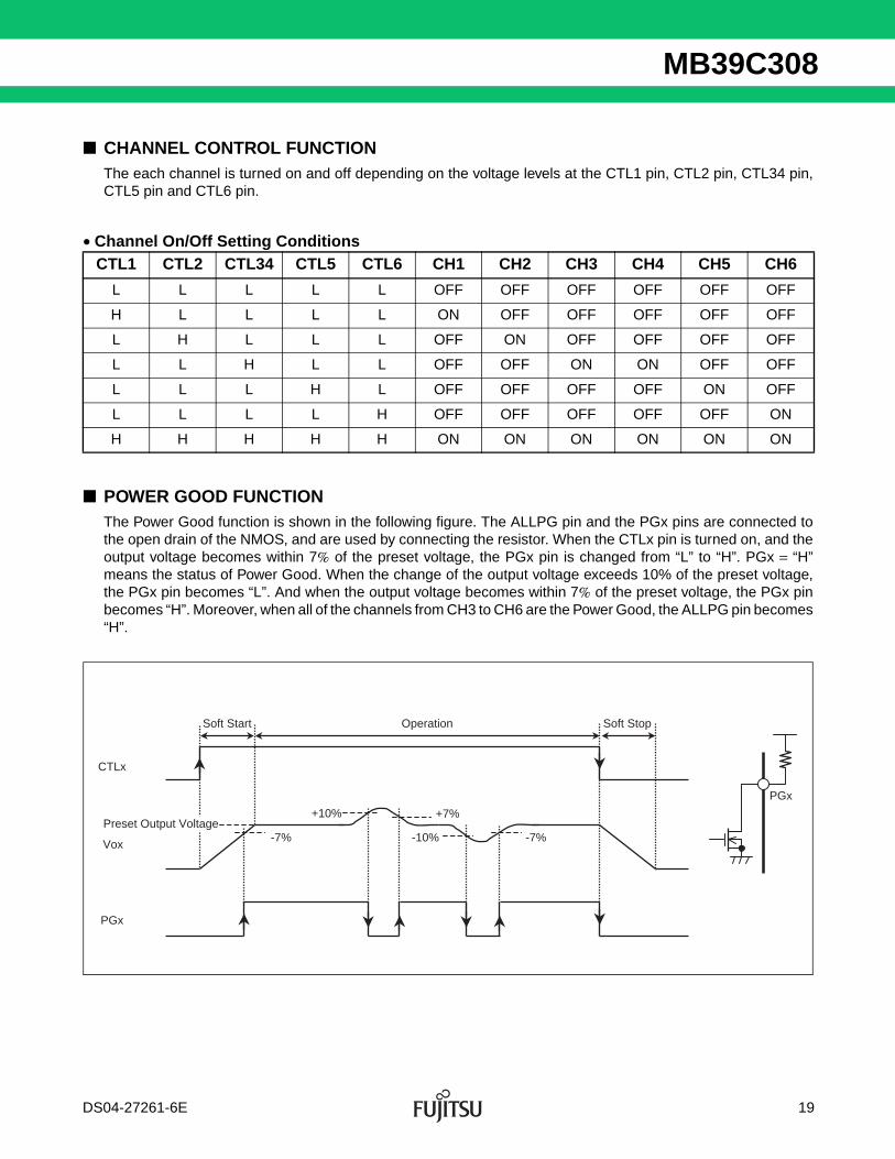
■ CHANNEL CONTROL FUNCTIONThe each channel is turned on and off depending on the voltage levels at the CTL1 pin, CTL2 pin, CTL34 pin,CTL5 pin and CTL6 pin.
• Channel On/Off Setting Conditions
■ POWER GOOD FUNCTIONThe Power Good function is shown in the following figure. The ALLPG pin and the PGx pins are connected tothe open drain of the NMOS, and are used by connecting the resistor. When the CTLx pin is turned on, and theoutput voltage becomes within 7% of the preset voltage, the PGx pin is changed from “L” to “H”. PGx = “H”means the status of Power Good. When the change of the output voltage exceeds 10% of the preset voltage,the PGx pin becomes “L”. And when the output voltage becomes within 7% of the preset voltage, the PGx pinbecomes “H”. Moreover, when all of the channels from CH3 to CH6 are the Power Good, the ALLPG pin becomes“H”.
CTL1 CTL2 CTL34 CTL5 CTL6 CH1 CH2 CH3 CH4 CH5 CH6
L L L L L OFF OFF OFF OFF OFF OFF
H L L L L ON OFF OFF OFF OFF OFF
L H L L L OFF ON OFF OFF OFF OFF
L L H L L OFF OFF ON ON OFF OFF
L L L H L OFF OFF OFF OFF ON OFF
L L L L H OFF OFF OFF OFF OFF ON
H H H H H ON ON ON ON ON ON
CTLx
Vox
PGx
OperationSoft Start Soft Stop
Preset Output Voltage+7%
-10%
+10%
-7% -7%
PGx
DS04-27261-6E 19
MB39C308
■ PROTECTION<1> Under Voltage Lock Out Protection (UVLO)
The UVLO prevents IC malfunctions or system damage and the degradation caused by the excessive voltageor instantaneous voltage drop of the power supply voltage (AVDD), bias voltage (VB), internal reference voltage(VREF). The UVLO turns off all the high- and low-side FETs of CH1 to CH6 when the AVDD pin drops below 5.0 V(Typ).The UVLO is released when the AVDD pin is above 5.1 V (Typ). This is the non-latch type protection.
<2> Input Over Voltage Protection (IVP)
The circuit prevents IC malfunctions or system damage and the degradation caused by the excessive voltageor instantaneous voltage drop of the power supply voltage (AVDD). The IVP turns off all the high- and low-side FETs of CH1 to CH6 when the AVDD pin exceeds 13.0 V(Typ). TheIVP is released when the AVDD pin drops below 12.85 V (Typ). This is the non-latch type protection.
<3> Over Temperature Protection (OTP)
The OTP prevents thermal damages on ICs. The IVP function turns off all the high- and low-side FETs of CH1to CH6 when the junction temperature exceeds +150 °C (Typ). The OPT is released when the temperature dropsbelow +125 °C (Typ). This is the non-latch type protection.
<4> Output Short Circuit Protection (SCP)
The SCP function stops outputting data when the output voltage falls and protects the devices connected tooutputs. The SCP timer will start to count when either of output voltages CH1 to CH6 falls due to the output short-circuitto GND or excessive currents. The SCP function starts to operate the latch protection and turns off all the high-and low-side FETs when the output voltage continues to fall to 1.4 ms (Typ). Follow either of the steps to release the latch of output short circuit protection.
- After all of CTL signals from CH1 to CH6 are set to “L” level, turn on the each CTL signal again. - When the voltage of the AVDD pin is below the threshold voltage of the UVLO, and then the voltage of the
AVDD pin becomes higher than the threshold voltage of UVLO again, the each output will start up.
<5> Output Over Voltage Protection (OVP)
The OVP protects the devices which are connected to outputs when the output voltage rises. When either outputvoltage of the CH1 to CH6 is higher than 120% of each channel's preset voltage (Typ), the OVP turns off all thehigh- and low-side FETs of the channels (However, the only CH4 is turned off the high-side FET and turned onthe low-side FET. The CH4 logic is different from other channels as it is controlled with PWM). The OVP isreleased when the output voltage is below 103% of the preset voltage (Typ). This is the non-latch type protection.
<6> Over Current Protection (OCP)
The OCP function controls the output current. When drain-to-source current excessively increases, the OCPcontrols the output current to the preset value for each channel. Then, because of the OCP functions, the outputvoltage usually drops. As a result, the SCP stop the all outputs with the latch setting. The OCP functions only for the corresponding channels only, however, the SCP stops all of the channels in theend.
20 DS04-27261-6E
MB39C308
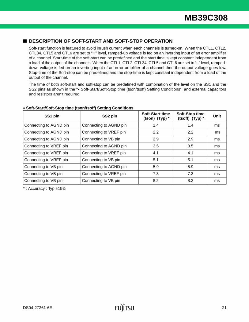
■ DESCRIPTION OF SOFT-START AND SOFT-STOP OPERATIONSoft-start function is featured to avoid inrush current when each channels is turned-on. When the CTL1, CTL2,CTL34, CTL5 and CTL6 are set to “H” level, ramped-up voltage is fed on an inverting input of an error amplifierof a channel. Start-time of the soft-start can be predefined and the start time is kept constant independent froma load of the output of the channels. When the CTL1, CTL2, CTL34, CTL5 and CTL6 are set to “L” level, ramped-down voltage is fed on an inverting input of an error amplifier of a channel then the output voltage goes low.Stop-time of the Soft-stop can be predefined and the stop-time is kept constant independent from a load of theoutput of the channel.
The time of both soft-start and soft-stop can be predefined with combination of the level on the SS1 and theSS2 pins as shown in the “• Soft-Start/Soft-Stop time (tson/tsoff) Setting Conditions”, and external capacitorsand resistors aren't required
• Soft-Start/Soft-Stop time (tson/tsoff) Setting Conditions
* : Accuracy : Typ ±15%
SS1 pin SS2 pin Soft-Start time (tson) (Typ) *
Soft-Stop time (tsoff) (Typ) * Unit
Connecting to AGND pin Connecting to AGND pin 1.4 1.4 ms
Connecting to AGND pin Connecting to VREF pin 2.2 2.2 ms
Connecting to AGND pin Connecting to VB pin 2.9 2.9 ms
Connecting to VREF pin Connecting to AGND pin 3.5 3.5 ms
Connecting to VREF pin Connecting to VREF pin 4.1 4.1 ms
Connecting to VREF pin Connecting to VB pin 5.1 5.1 ms
Connecting to VB pin Connecting to AGND pin 5.9 5.9 ms
Connecting to VB pin Connecting to VREF pin 7.3 7.3 ms
Connecting to VB pin Connecting to VB pin 8.2 8.2 ms
DS04-27261-6E 21
MB39C308
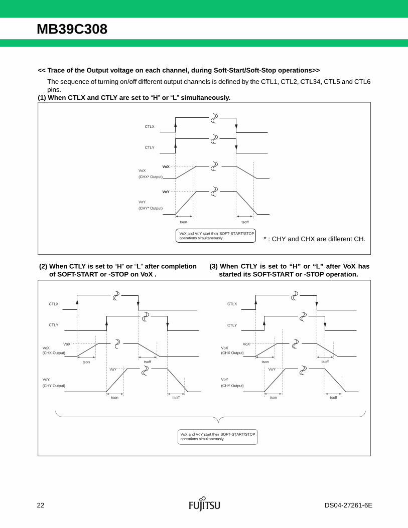
<< Trace of the Output voltage on each channel, during Soft-Start/Soft-Stop operations>>
The sequence of turning on/off different output channels is defined by the CTL1, CTL2, CTL34, CTL5 and CTL6pins.
(1) When CTLX and CTLY are set to “H” or “L” simultaneously.
(2) When CTLY is set to “H” or “L” after completion of SOFT-START or -STOP on VoX .
(3) When CTLY is set to “H” or “L” after VoX hasstarted its SOFT-START or -STOP operation.
CTLY
CTLX
VoX
(CHX* Output)
VoX
VoY
VoY
(CHY* Output)
VoX and VoY start their SOFT-START/STOP operations simultaneously.
VoX
VoY
tson tsoff
* : CHY and CHX are different CH.
CTLY
CTLX
VoX(CHX Output)
VoY
(CHY Output)
CTLY
CTLX
VoX(CHX Output)
VoY
(CHY Output)
VoX and VoY start their SOFT-START/STOP operations simultaneously.
VoX
VoY
tson
tsofftson
tsoff
VoX
VoY
tson
tsofftson
tsoff
22 DS04-27261-6E
MB39C308
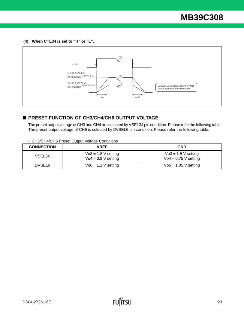
■ PRESET FUNCTION OF CH3/CH4/CH6 OUTPUT VOLTAGEThe preset output voltage of CH3 and CH4 are selected by VSEL34 pin condition. Please refer the following table.The preset output voltage of CH6 is selected by DVSEL6 pin condition. Please refer the following table.
• CH3/CH4/CH6 Preset Output Voltage Conditions
(4) When CTL34 is set to “H” or “L”.
CONNECTION VREF GND
VSEL34Vo3 = 1.8 V setting Vo4 = 0.9 V setting
Vo3 = 1.5 V setting Vo4 = 0.75 V setting
DVSEL6 Vo6 = 1.1 V setting Vo6 = 1.05 V setting
CTL34
Vo3 (1.8 V/1.5 V)
(CH3 Output)
(0.9 V/0.75 V)
(1.8 V/1.5 V)
Vo4 (0.9 V/0.75 V)
(CH4 Output) Vo3 and Vo4 starts its SOFT-START/STOP operation simultaneously.
tson tsoff
DS04-27261-6E 23
MB39C308
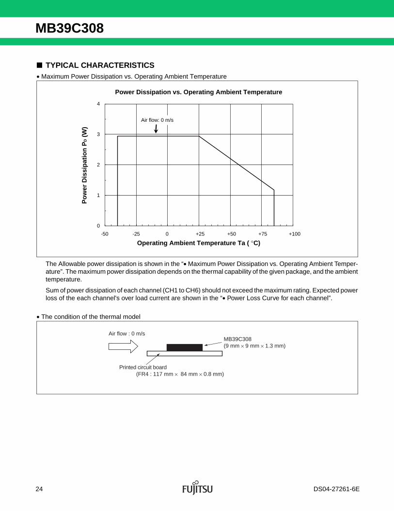
■ TYPICAL CHARACTERISTICS• Maximum Power Dissipation vs. Operating Ambient Temperature
The Allowable power dissipation is shown in the “• Maximum Power Dissipation vs. Operating Ambient Temper-ature”. The maximum power dissipation depends on the thermal capability of the given package, and the ambienttemperature.
Sum of power dissipation of each channel (CH1 to CH6) should not exceed the maximum rating. Expected powerloss of the each channel's over load current are shown in the “• Power Loss Curve for each channel”.
• The condition of the thermal model
0
1
2
3
4
-50 -25 0 +25 +50 +75 +100
Air flow: 0 m/s
Power Dissipation vs. Operating Ambient Temperature
Operating Ambient Temperature Ta ( °C)
Po
wer
Dis
sip
atio
n P
D (
W)
Printed circuit board(FR4 : 117 mm × 84 mm × 0.8 mm)
MB39C308(9 mm × 9 mm × 1.3 mm)
Air flow : 0 m/s
24 DS04-27261-6E
MB39C308
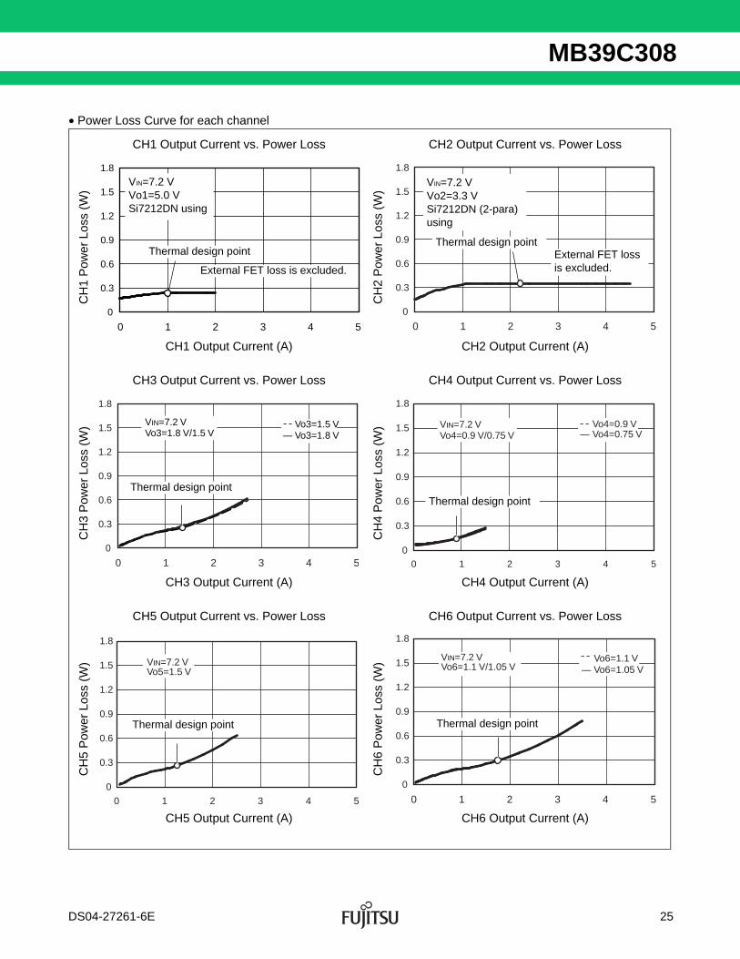
• Power Loss Curve for each channel
CH1 Output Current vs. Power Loss CH2 Output Current vs. Power Loss
CH
1 P
ower
Los
s (W
)
CH
2 P
ower
Los
s (W
)
CH1 Output Current (A) CH2 Output Current (A)
CH3 Output Current vs. Power Loss CH4 Output Current vs. Power Loss
CH
3 P
ower
Los
s (W
)
CH
4 P
ower
Los
s (W
)
CH3 Output Current (A) CH4 Output Current (A)
CH5 Output Current vs. Power Loss CH6 Output Current vs. Power Loss
CH
5 P
ower
Los
s (W
)
CH
6 P
ower
Los
s (W
)
CH5 Output Current (A) CH6 Output Current (A)
0
0.3
0.6
0.9
1.2
1.5
1.8
0 1 2 3 4 5
VIN=7.2 VVo1=5.0 VSi7212DN using
External FET loss is excluded.
Thermal design point
0
0.3
0.6
0.9
1.2
1.5
1.8
0 1 2 3 4 5
External FET loss is excluded.
VIN=7.2 VVo2=3.3 VSi7212DN (2-para) using
Thermal design point
0.3
0.6
0.9
1.2
1.5
1.8
0 1 2 3 4 5
Vo3=1.5 VVo3=1.8 V
VIN=7.2 VVo3=1.8 V/1.5 V
0
Thermal design point
0
0.3
0.6
0.9
1.2
1.5
1.8
0 1 2 3 4 5
Vo4=0.9 VVo4=0.75 V
VIN=7.2 VVo4=0.9 V/0.75 V
Thermal design point
0
0.3
0.6
0.9
1.2
1.5
1.8
0 1 2 3 4 5
VIN=7.2 VVo5=1.5 V
Thermal design point
0
0.3
0.6
0.9
1.2
1.5
1.8
0 1 2 3 4 5
Vo6=1.1 VVIN=7.2 VVo6=1.1 V/1.05 V Vo6=1.05 V
Thermal design point
DS04-27261-6E 25
MB39C308
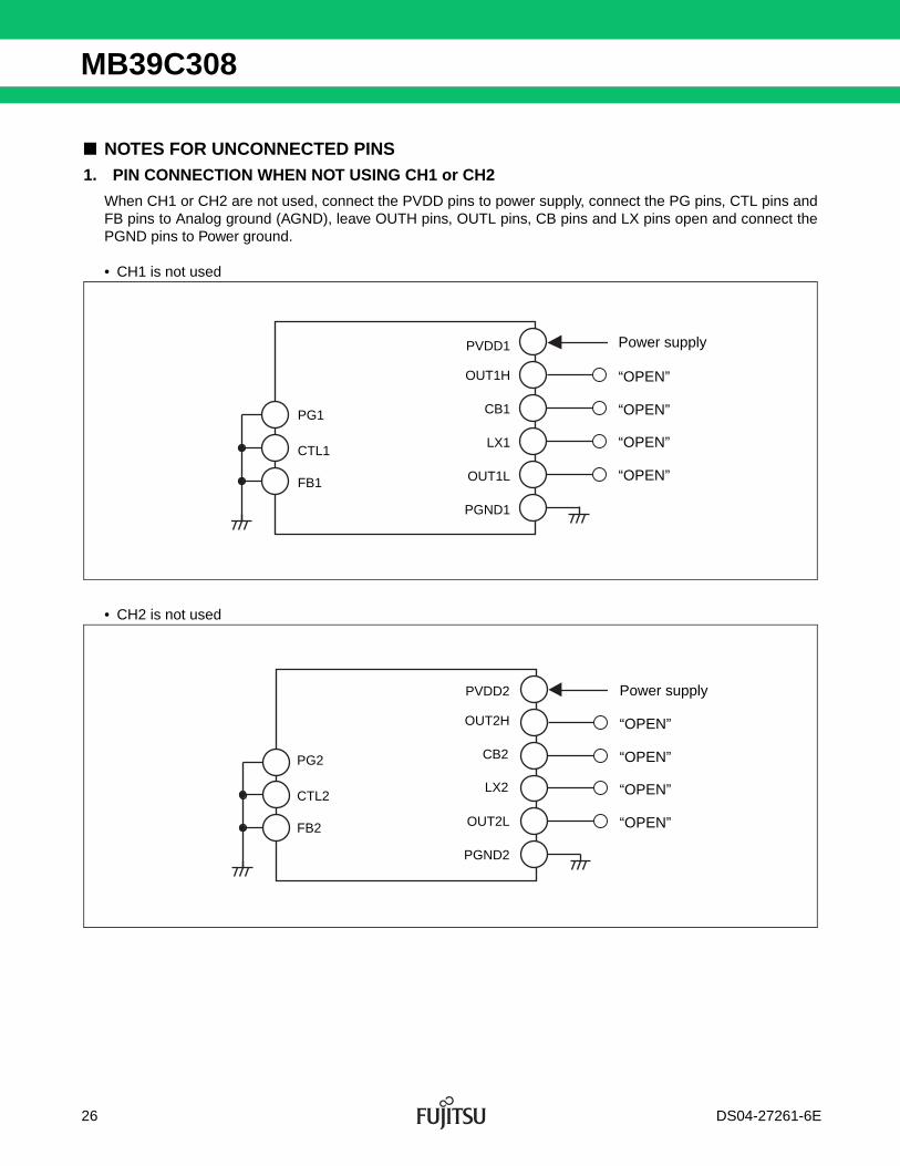
■ NOTES FOR UNCONNECTED PINS1. PIN CONNECTION WHEN NOT USING CH1 or CH2
When CH1 or CH2 are not used, connect the PVDD pins to power supply, connect the PG pins, CTL pins andFB pins to Analog ground (AGND), leave OUTH pins, OUTL pins, CB pins and LX pins open and connect thePGND pins to Power ground.
• CH1 is not used
• CH2 is not used
1
PG1
PVDD1
OUT1H
CB1
LX1
OUT1L
PGND1
CTL1
FB1
Power supply
“OPEN”
“OPEN”
“OPEN”
“OPEN”
1
PG2
PVDD2
OUT2H
CB2
LX2
OUT2L
PGND2
CTL2
FB2
Power supply
“OPEN”
“OPEN”
“OPEN”
“OPEN”
26 DS04-27261-6E
MB39C308
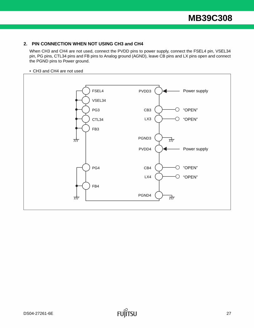
2. PIN CONNECTION WHEN NOT USING CH3 and CH4
When CH3 and CH4 are not used, connect the PVDD pins to power supply, connect the FSEL4 pin, VSEL34pin, PG pins, CTL34 pins and FB pins to Analog ground (AGND), leave CB pins and LX pins open and connectthe PGND pins to Power ground.
• CH3 and CH4 are not used
FSEL4
VSEL34
PG3
CTL34
FB3
PG4 CB4
LX4
PGND3
PVDD4
CB3
PVDD3
PGND4
LX3
FB4
Power supply
“OPEN”
“OPEN”
Power supply
“OPEN”
“OPEN”
DS04-27261-6E 27
MB39C308
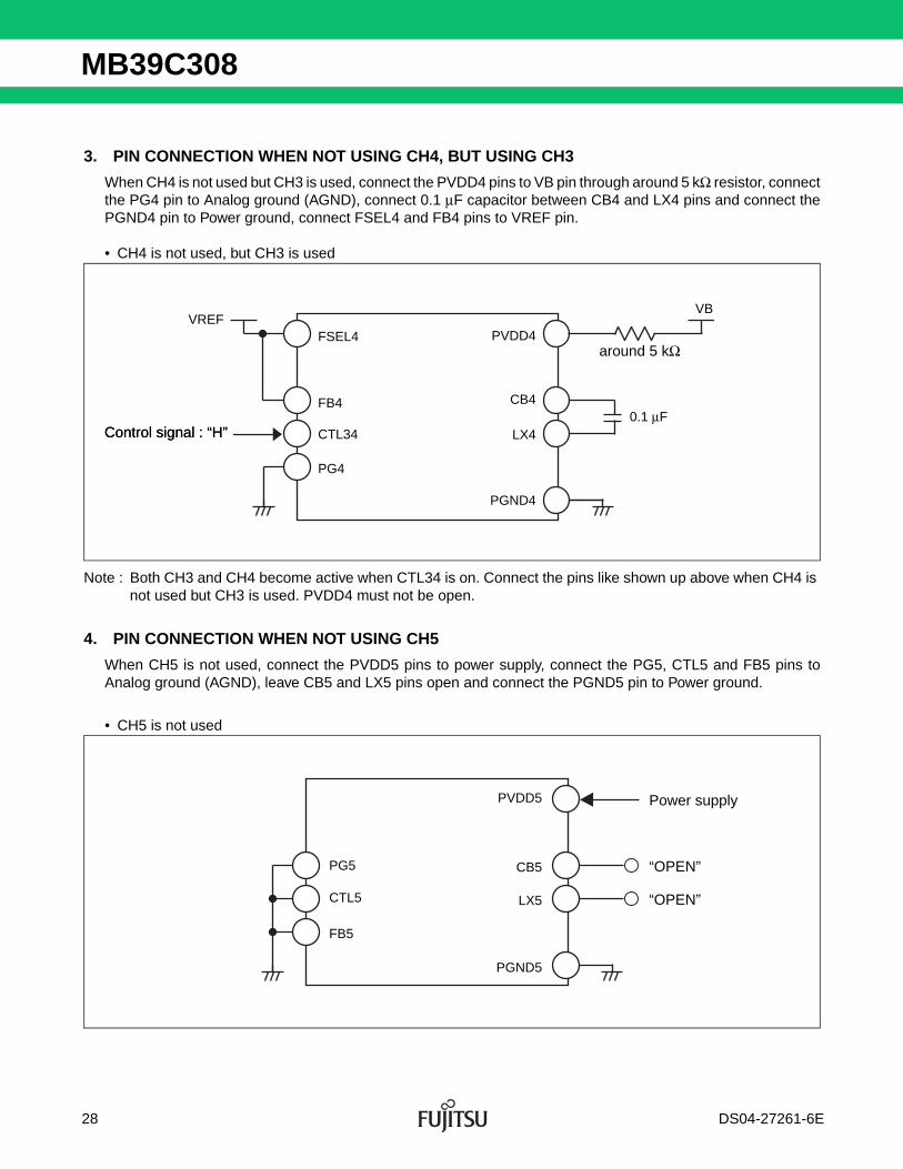
3. PIN CONNECTION WHEN NOT USING CH4, BUT USING CH3
When CH4 is not used but CH3 is used, connect the PVDD4 pins to VB pin through around 5 kΩ resistor, connectthe PG4 pin to Analog ground (AGND), connect 0.1 μF capacitor between CB4 and LX4 pins and connect thePGND4 pin to Power ground, connect FSEL4 and FB4 pins to VREF pin.
• CH4 is not used, but CH3 is used
Note : Both CH3 and CH4 become active when CTL34 is on. Connect the pins like shown up above when CH4 is not used but CH3 is used. PVDD4 must not be open.
4. PIN CONNECTION WHEN NOT USING CH5
When CH5 is not used, connect the PVDD5 pins to power supply, connect the PG5, CTL5 and FB5 pins toAnalog ground (AGND), leave CB5 and LX5 pins open and connect the PGND5 pin to Power ground.
• CH5 is not used
FSEL4 PVDD4VREF
VB
CB4
LX4
PGND4
FB4
CTL340.1 μF
PG4
Control signal : “H”Control signal : “H”
around 5 kΩ
PG5
CTL5
FB5
PGND5
LX5
CB5
PVDD5 Power supply
“OPEN”
“OPEN”
28 DS04-27261-6E
MB39C308
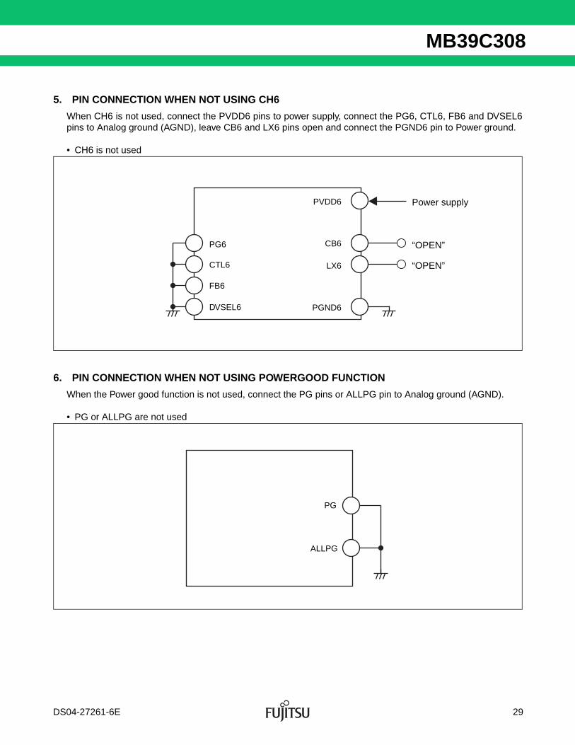
5. PIN CONNECTION WHEN NOT USING CH6
When CH6 is not used, connect the PVDD6 pins to power supply, connect the PG6, CTL6, FB6 and DVSEL6pins to Analog ground (AGND), leave CB6 and LX6 pins open and connect the PGND6 pin to Power ground.
• CH6 is not used
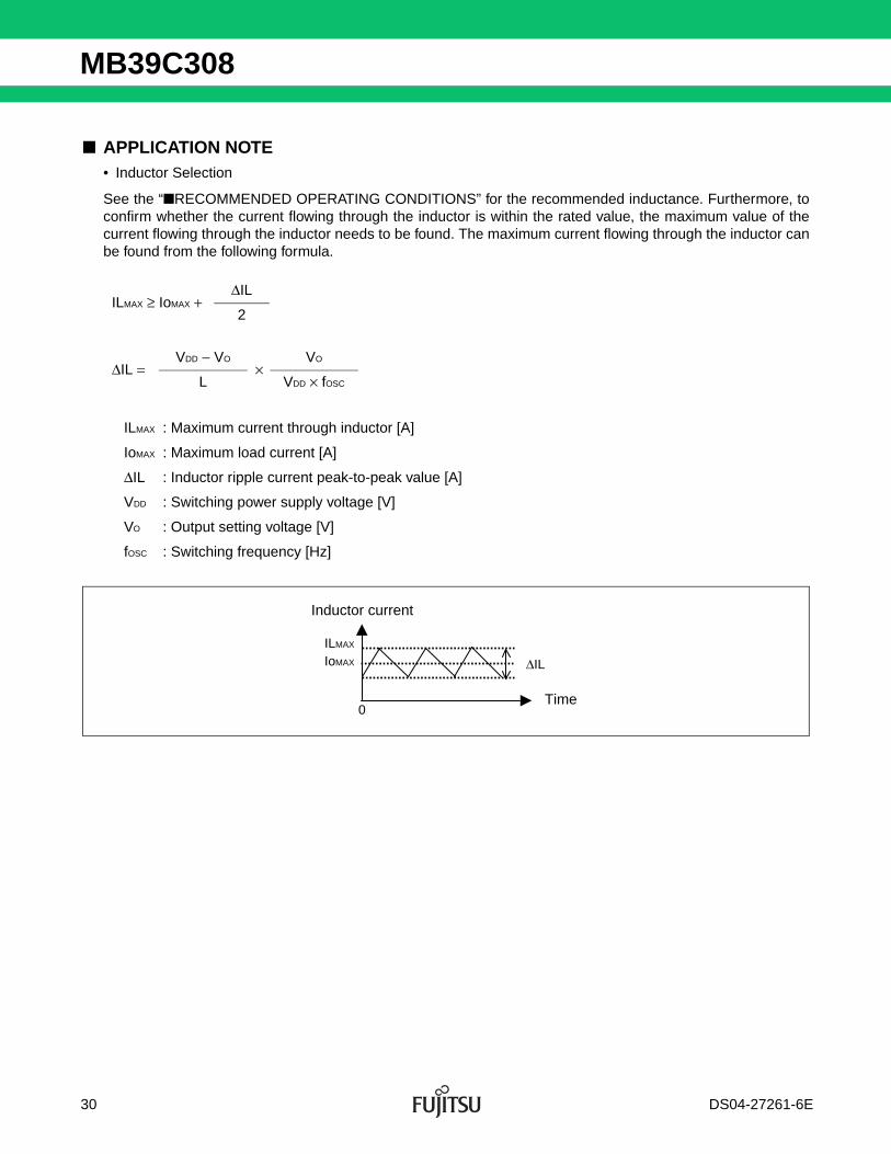
6. PIN CONNECTION WHEN NOT USING POWERGOOD FUNCTION
When the Power good function is not used, connect the PG pins or ALLPG pin to Analog ground (AGND).
• PG or ALLPG are not used
PG6
PVDD6
CB6
LX6
PGND6
CTL6
FB6
DVSEL6
Power supply
“OPEN”
“OPEN”
PG
ALLPG
DS04-27261-6E 29
MB39C308
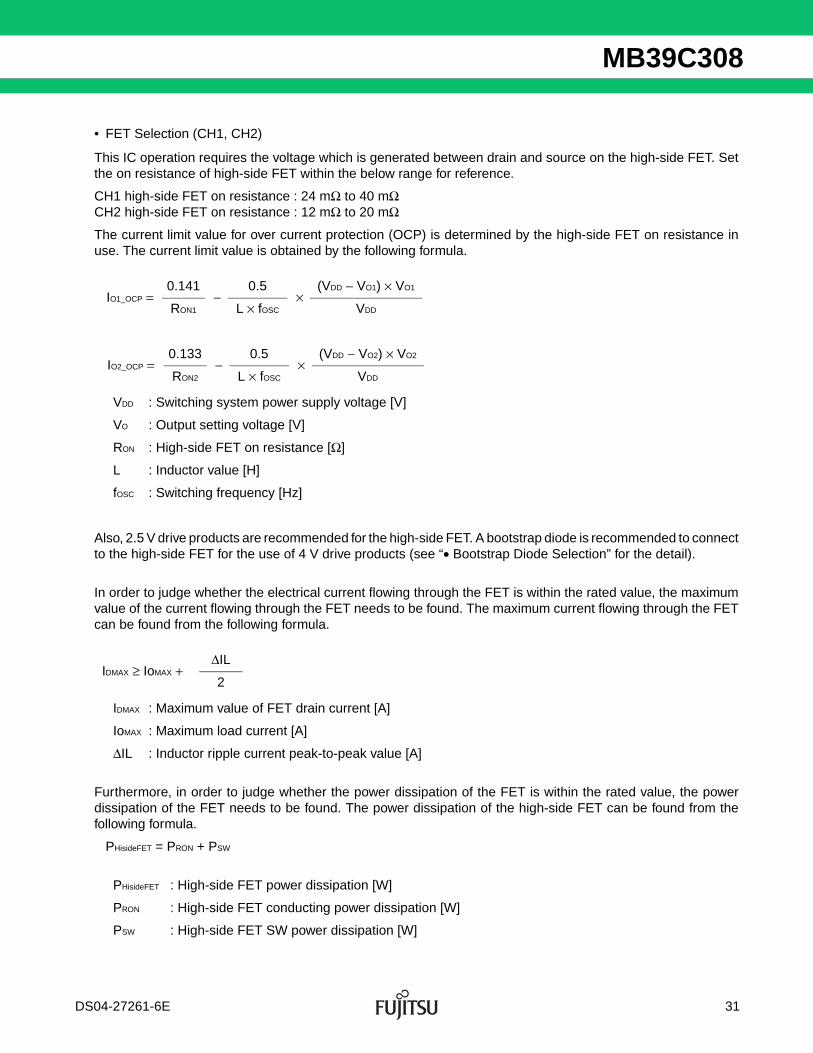
■ APPLICATION NOTE• Inductor Selection
See the “■RECOMMENDED OPERATING CONDITIONS” for the recommended inductance. Furthermore, toconfirm whether the current flowing through the inductor is within the rated value, the maximum value of thecurrent flowing through the inductor needs to be found. The maximum current flowing through the inductor canbe found from the following formula.
ILMAX : Maximum current through inductor [A]
IoMAX : Maximum load current [A]
ΔIL : Inductor ripple current peak-to-peak value [A]
VDD : Switching power supply voltage [V]
VO : Output setting voltage [V]
fOSC : Switching frequency [Hz]
ILMAX ≥ IoMAX + ΔIL
2
ΔIL = VDD − VO
× VO
L VDD × fOSC
ILMAX
IoMAX ΔIL
0
Inductor current
Time
30 DS04-27261-6E
MB39C308
• FET Selection (CH1, CH2)
This IC operation requires the voltage which is generated between drain and source on the high-side FET. Setthe on resistance of high-side FET within the below range for reference.
CH1 high-side FET on resistance : 24 mΩ to 40 mΩ CH2 high-side FET on resistance : 12 mΩ to 20 mΩ
The current limit value for over current protection (OCP) is determined by the high-side FET on resistance inuse. The current limit value is obtained by the following formula.
VDD : Switching system power supply voltage [V]
VO : Output setting voltage [V]
RON : High-side FET on resistance [Ω]
L : Inductor value [H]
fOSC : Switching frequency [Hz]
Also, 2.5 V drive products are recommended for the high-side FET. A bootstrap diode is recommended to connectto the high-side FET for the use of 4 V drive products (see “• Bootstrap Diode Selection” for the detail).
In order to judge whether the electrical current flowing through the FET is within the rated value, the maximumvalue of the current flowing through the FET needs to be found. The maximum current flowing through the FETcan be found from the following formula.
IDMAX : Maximum value of FET drain current [A]
IoMAX : Maximum load current [A]
ΔIL : Inductor ripple current peak-to-peak value [A]
Furthermore, in order to judge whether the power dissipation of the FET is within the rated value, the powerdissipation of the FET needs to be found. The power dissipation of the high-side FET can be found from thefollowing formula.
PHisideFET = PRON + PSW
PHisideFET : High-side FET power dissipation [W]
PRON : High-side FET conducting power dissipation [W]
PSW : High-side FET SW power dissipation [W]
IO1_OCP = 0.141
− 0.5
× (VDD − VO1) × VO1
RON1 L × fOSC VDD
IO2_OCP = 0.133
− 0.5
× (VDD − VO2) × VO2
RON2 L × fOSC VDD
IDMAX ≥ IoMAX + ΔIL
2
DS04-27261-6E 31

MB39C308
High-side FET conducting power dissipation
PRON : High-side FET conducting power dissipation [W]
IoMAX : Maximum load current [A]
VDD : Switching system power supply voltage [V]
VO : Output setting voltage [V]
RON : High-side FET on resistance [Ω]
High-side FET switching power dissipation
PSW : Switching power dissipation [W]
VDD : Switching system power supply voltage [V]
fOSC : Switching frequency (Hz)
Ibtm : Inductor ripple current bottom value [A]
Itop : Inductor ripple current top value [A]
tr : High-side FET turn-on time [s]
tf : High-side FET turn-off time [s]
tr and tf can be found simply from the following formula.
Qgd : Gate-Drain charge of High-side FET [C]
Vth : High-side FET threshold voltage [V]
The power dissipation of the Low-side FET can be found from the following formula.
PRon : Low-side FET conducting power dissipation [W]
IoMAX : Maximum load current [A]
VDD : Switching power supply voltage [V]
VO : Output setting voltage [V]
Ron : Low-side FET on resistance [Ω]
Note : The transition voltage of the voltage between the drain and source of the Low-side FET is generally small and the switching power loss is negligible. Therefore it has been omitted from this formula.
PRON = (IoMAX) 2 × VO
× RONVDD
PSW = VDD × fOSC × (Ibtm × tr + Itop × tf)
2
tr = Qgd × 12
tf = Qgd × 12
5 − Vth Vth
PLosideFET = PRon = (IOMAX) 2 × (1VO
) × RonVDD
32 DS04-27261-6E
MB39C308
• Input Capacitor Selection
Because this IC uses the C-Mode system, it is recommended to use ceramic capacitors with a small ESR. Seethe “■ RECOMMENDED OPERATING CONDITIONS” for the value of the capacitance.
• Output Capacitor Selection
Because this IC uses the C-Mode system, it is recommended to use ceramic capacitors with a small ESR. Seethe “■ RECOMMENDED OPERATING CONDITIONS” for the value of the capacitance.
• Bootstrap Diode Selection
It is not necessary to connect diode to the outside device normally because this device contains a bootstrapdiode. However, it is recommended to add a shotkey barrier diode (SBD) when 4 V drive products is used forCH1 and CH2 switching FET. In this case, select the smallest forward current possible and connect as the figurebelow.
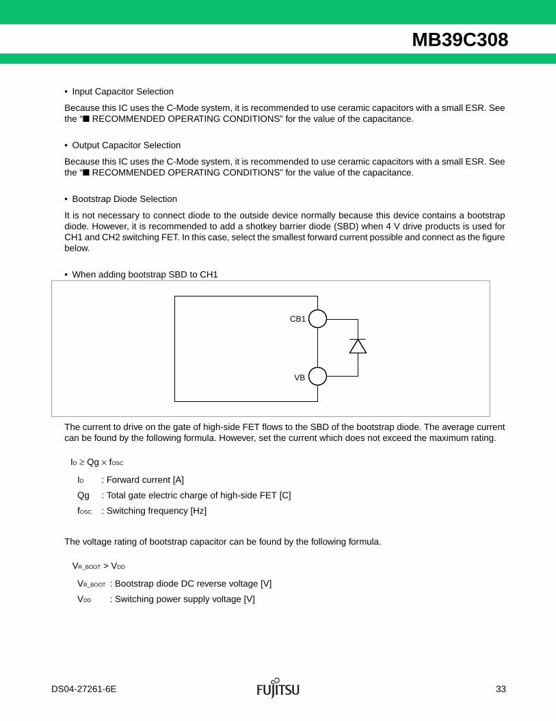
• When adding bootstrap SBD to CH1
The current to drive on the gate of high-side FET flows to the SBD of the bootstrap diode. The average currentcan be found by the following formula. However, set the current which does not exceed the maximum rating.
ID : Forward current [A]
Qg : Total gate electric charge of high-side FET [C]
fOSC : Switching frequency [Hz]
The voltage rating of bootstrap capacitor can be found by the following formula.
VR_BOOT : Bootstrap diode DC reverse voltage [V]
VDD : Switching power supply voltage [V]
ID ≥ Qg × fOSC
VR_BOOT > VDD
VB
CB1
DS04-27261-6E 33
MB39C308
• Bootstrap Capacitor Selection
Although the default bootstrap capacitor (the capacitor between CB and LX) is 0.1μF, this may need to be adjustedif the FET used on CH1 and CH2 have a large Qg. The bootstrap capacitor needs to be able to charge sufficientlyto drive the gate of the High-side FET. As a rough guide, select a capacitor with a minimum value of capacitancethat is able to accumulate approximately 10 times the charge of the Qg of the High-side FET.
CCB : Bootstrap capacitance [F]
Qg : High-side SWFET gate charge [C]
VCB : CB voltage (4.3 V)
• VB Capacitor Selection
Although the default VB capacitor is 1 μF, this may need to be adjusted if the FET used on CH1 and CH2 havea large Qg. The VB capacitor needs to be able to charge sufficiently to drive the gate of the High-side FET. Asa rough guide, select a capacitor with a minimum value of capacitance that is able to accumulate approximately50 times the charge of the Qg of the High-side FET.
CVB : VB capacitance [F]
QgH12 : Total gate charge of High-side FET for CH1 and CH2 [C] (Total when Vgs = 4.3 V)
QgL12 : Total gate charge of Low-side FET for CH1 and CH2 [C] (Total when Vgs = 5 V)
VVB : VB voltage (5 V)
VCB : CB voltage (4.3 V)
CCB ≥ 10 × Qg
VCB
CVB ≥ 50 × QgH12 + 9.3 × 10⁻⁹
+ QgL12 + 23 × 10-9
VCB VVB( (
34 DS04-27261-6E
MB39C308
• Power Dissipation and Thermal Design
Although these does not need to be examined in most cases because the IC is highly efficient, Dissipation andthe thermal design may need to be investigate if the IC is used with high power supply voltages, high oscillatorfrequencies, high loads, or at high temperatures.
The internal IC power dissipation (PIC) can be found from the following formula.
PIC = VDD × (IDD + Qg12 + 32 × 10-9) × fOSC + PHisideFET3-6 + PLosideFET3-6
PIC : Internal IC power dissipation [W]
VDD : Power supply voltage (VIN) [V]
IDD : Power supply current [A] (250 μA Typ)
Qg12 : Total gate charge of High-side FET (VGS = 4.3 V) and Low-side FET (VGS = 5 V) for CH1 and CH2 [C]
fOSC : Switching frequency [Hz]
PHisideFET3-6 : Total High-side SWFET power dissipation of internal High-side FET [W]
PLosideFET3-6 : Total Low-side SWFET power dissipation of internal Low-side FET [W]
Furthermore, the power dissipation of the High-side FET of each built-in channel can be found from the followingformula.
PHisideFET = PRON + PSW
PHisideFET : High-side FET power dissipation [W]
PRON : High-side FET conducting power dissipation [W]
PSW : High-side FET switching power dissipation [W]
High-side FET conducting power dissipation
PRON : High-side FET conducting power dissipation [W]
IoMAX : Maximum load current [A]
VDD : Switching power supply voltage [V]
VO : Output setting voltage [V]
RON : On resistance of High-side FET [Ω]
PRON = (IoMAX) 2VO
× RONVDD
DS04-27261-6E 35
MB39C308
High-side FET switching power dissipation
PSW : SW power dissipation [W]
VDD : Switching system power supply voltage [V]
fOSC : Oscillation frequency (Hz)
Ibtm : Inductor ripple current bottom value [A]
Itop : Inductor ripple current top value [A]
tr : High-side FET turn-on time [s]
tf : High-side FET turn-off time [s]
tr and tf are simply given by the following values.
The power dissipation of the Low-side FET can be found from the following formula.
PRon : Low-side FET conducting power dissipation [W]
IoMAX : Maximum load current [A]
VDD : Switching system power supply voltage [V]
VO : Output setting voltage [V]
Ron : Low-side FET on resistance [Ω]
Note : The transition voltage of the voltage between the drain and source of the Low-side FET is generally small and the switching power loss is negligible. Therefore it has been omitted from this formula.
The junction temperature (Tj) can be found from the following formula.
Tj = Ta + θja × PIC
Tj : Junction temperature [ °C] ( + 125 °C Max)
Ta : Ambient temperature [ °C]
θja : PFBGA-208 package thermal resistance (34 °C/W)
PIC : IC power dissipation [W]
PSW = VDD × fOSC × (Ibtm × tr + Itop × tf)
2
tr = 4 ns tf = 4 ns
PRon = (IOMAX)2 × (1 − VO
) × RonVDD
36 DS04-27261-6E
MB39C308
■ REFERENCE DATA• Efficiency vs. load current
60
65
70
75
80
85
90
95
100
0.01 0.1 1 10
CH1 η1 - IO1
60
65
70
75
80
85
90
95
100
0.01 0.1 1 10
CH2 η2 - IO2
60
65
70
75
80
85
90
95
100
0.01 0.1 1 10
Vo3 = 1.8 VVo3 = 1.5 V
CH3 η3 - IO3
60
65
70
75
80
85
90
95
100
0.01 0.1 1 10
fosc = 700 kHz, VO4 = 0.9 Vfosc = 700 kHz, VO4 = 0.75 Vfosc = 350 kHz, VO4 = 0.9 Vfosc = 350 kHz, VO4 = 0.75 V
CH4 η4 - IO4
60
65
70
75
80
85
90
95
100
0.01 0.1 1 10
CH5 η5 - IO5
60
65
70
75
80
85
90
95
100
0.01 0.1 1 10
VO6 = 1.05 VVO6 = 1.1 V
CH6 η6 - IO6
Load current IO1 (A)
effic
ienc
y η1
(%
)
Load current IO2 (A)ef
ficie
ncy
η2 (
%)
Load current IO3 (A)
effic
ienc
y η3
(%
)
Load current IO4 (A)
effic
ienc
y η4
(%
)
Load current IO5 (A)
effic
ienc
y η5
(%
)
Load current IO6 (A)
effic
ienc
y η6
(%
)
DS04-27261-6E 37
MB39C308
• Load regulation
(Continued)
Ta = + 25°CVO1 = 5.0 Vfosc = 700 kHz
CH1 VO1 vs. IO1
Ta = + 25°CVO2 = 3.3 Vfosc = 700 kHz
CH2 VO2 vs. IO2
Ta = + 25°CVO3 = 1.5 Vfosc = 700 kHz
CH3 VO3 vs. IO3
Ta = + 25°CVO3 = 1.8 Vfosc = 700 kHz
CH3 VO3 vs. IO3
Ta = + 25°CVO4 = 0.75 V
fosc = 350 kHzfosc = 700 kHz
CH4 VO4 vs. IO4
Ta = + 25°CVO4 = 0.9 V
CH4 VO4 vs. IO4
fosc = 350 kHzfosc = 700 kHz
Load current IO1 (A)
Out
put v
olta
ge V
O1
(V)
Load current IO3 (A)
Out
put v
olta
ge V
O3
(V)
Load current IO3 (A)
Out
put v
olta
ge V
O3
(V)
Load current IO2 (A)
Out
put v
olta
ge V
O2
(V)
Load current IO4 (A)
Out
put v
olta
ge V
O4
(V)
Load current IO4 (A)
Out
put v
olta
ge V
O4
(V)
38 DS04-27261-6E
MB39C308
(Continued)
Ta = + 25°CVO5 = 1.5 Vfosc = 700 kHz
CH5 VO5 vs. IO5
Ta = + 25°CVO6 = 1.05 Vfosc = 700 kHz
CH6 VO6 vs. IO6
Ta = + 25°CVO6 = 1.1 Vfosc = 700 kHz
CH6 VO6 vs. IO6
Load current IO5 (A)
Out
put v
olta
ge V
O5
(V)
Load current IO6 (A)
Out
put v
olta
ge V
O6
(V)
Load current IO6 (A)
Out
put v
olta
ge V
O6
(V)
DS04-27261-6E 39
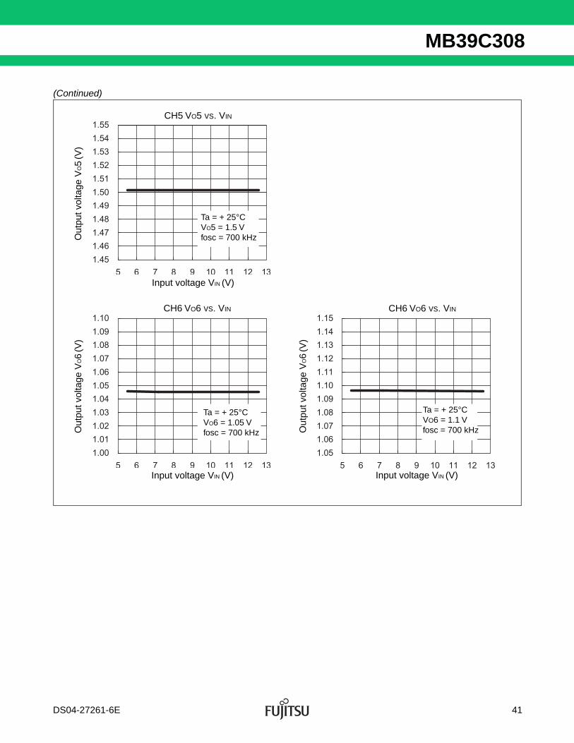
MB39C308
• Line regulation
(Continued)
Ta = + 25°CVO1 = 5.0 Vfosc = 700 kHz
CH1 VO1 vs. VIN CH2 VO2 vs. VIN
Ta = + 25°CVO2 = 3.3 Vfosc = 700 kHz
CH3 VO3 vs. VIN
Ta = + 25°CVO3 = 1.5 Vfosc = 700 kHz
CH3 VO3 vs. VIN
Ta = + 25°CVO3 = 1.8 Vfosc = 700 kHz
CH4 VO4 vs. VIN
fosc = 350 kHzfosc = 700 kHz
Ta = + 25°CVO4 = 0.75 V
CH4 VO4 vs. VIN
Ta = + 25°CVO4 = 0.9 V
fosc = 350 kHzfosc = 700 kHz
Input voltage VIN (V)
Out
put v
olta
ge V
O1
(V)
Input voltage VIN (V)
Out
put v
olta
ge V
O2
(V)
Input voltage VIN (V)
Out
put v
olta
ge V
O3
(V)
Input voltage VIN (V)
Out
put v
olta
ge V
O3
(V)
Input voltage VIN (V)
Out
put v
olta
ge V
O4
(V)
Input voltage VIN (V)
Out
put v
olta
ge V
O4
(V)
40 DS04-27261-6E
MB39C308
(Continued)
CH5 VO5 vs. VIN
Ta = + 25°CVO5 = 1.5 Vfosc = 700 kHz
CH6 VO6 vs. VIN
Ta = + 25°CVO6 = 1.05 Vfosc = 700 kHz
CH6 VO6 vs. VIN
Ta = + 25°CVO6 = 1.1 Vfosc = 700 kHz
Input voltage VIN (V)
Out
put v
olta
ge V
O5
(V)
Input voltage VIN (V)
Out
put v
olta
ge V
O6
(V)
Input voltage VIN (V)
Out
put v
olta
ge V
O6
(V)
DS04-27261-6E 41
MB39C308
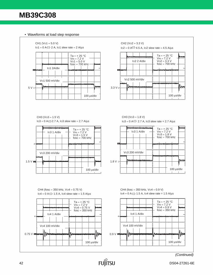
• Waveforms at load step response
(Continued)
CH1 (VO1 = 5.0 V)
IO1 = 0 A 2 A, IO1 slew rate = 2 A/μs
Ta = + 25 °CVIN = 7.2 VVO1 = 5.0 Vfosc = 700 kHz
IO1 2A/div
VO1 500 mV/div
100 μs/div
5 V 1
4
CH2 (VO2 = 3.3 V)
IO2 = 0 A 4.5 A, IO2 slew rate = 4.5 A/μs
Ta = + 25 °CVIN = 7.2 VVO2 = 3.3 Vfosc = 700 kHz
IO2 2 A/div
VO2 500 mV/div
100 μs/div
1
4
3.3 V
CH3 (VO3 = 1.5 V)IO3 = 0 A 2.7 A, IO3 slew rate = 2.7 A/μs
Ta = + 25 °CVIN = 7.2 VVO3 = 1.5 Vfosc = 700 kHz
IO3 1 A/div
VO3 200 mV/div
100 μs/div
1
4
1.5 V
CH3 (VO3 = 1.8 V)
IO3 = 0 A 2.7 A, IO3 slew rate = 2.7 A/μs
Ta = + 25 °CVIN = 7.2 VVO3 = 1.8 Vfosc = 700 kHz
IO3 1 A/div
VO3 200 mV/div
100 μs/div
1
4
1.8 V
CH4 (fosc = 350 kHz, VO4 = 0.75 V)
IO4 = 0 A 1.5 A, IO4 slew rate = 1.5 A/μs
Ta = + 25 °CVIN = 7.2 VVO4 = 0.75 Vfosc = 350 kHz
IO4 1 A/div
VO4 100 mV/div
100 μs/div
1
4
0.75 V
CH4 (fosc = 350 kHz, VO4 = 0.9 V)IO4 = 0 A 1.5 A, IO4 slew rate = 1.5 A/μs
Ta = + 25 °CVIN = 7.2 VVO4 = 0.9 Vfosc = 350 kHz
IO4 1 A/div
VO4 100 mV/div
100 μs/div
1
4
0.9 V
42 DS04-27261-6E
MB39C308
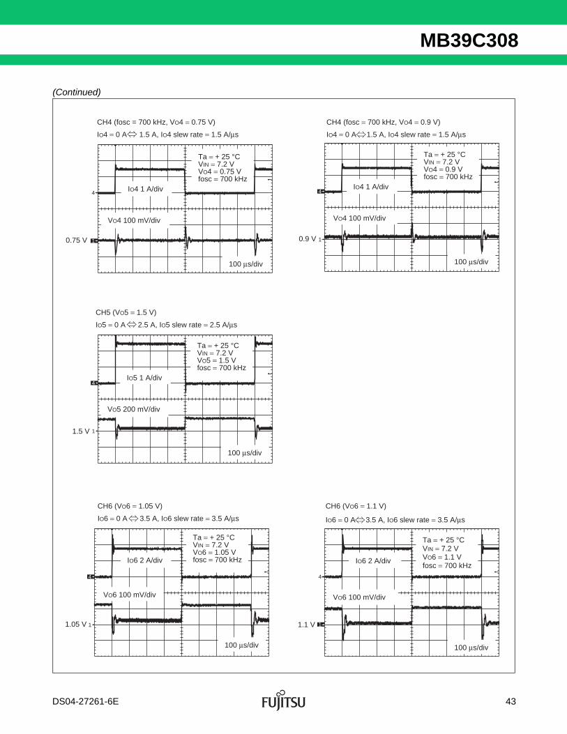
(Continued)
CH4 (fosc = 700 kHz, VO4 = 0.75 V)
IO4 = 0 A 1.5 A, IO4 slew rate = 1.5 A/μs
Ta = + 25 °CVIN = 7.2 VVO4 = 0.75 Vfosc = 700 kHz
IO4 1 A/div
VO4 100 mV/div
100 μs/div
0.75 V 1
4
CH4 (fosc = 700 kHz, VO4 = 0.9 V)
IO4 = 0 A 1.5 A, IO4 slew rate = 1.5 A/μs
Ta = + 25 °CVIN = 7.2 VVO4 = 0.9 Vfosc = 700 kHz
IO4 1 A/div
VO4 100 mV/div
100 μs/div
0.9 V 1
4
CH5 (VO5 = 1.5 V)
IO5 = 0 A 2.5 A, IO5 slew rate = 2.5 A/μs
Ta = + 25 °CVIN = 7.2 VVO5 = 1.5 Vfosc = 700 kHz
IO5 1 A/div
VO5 200 mV/div
100 μs/div
1.5 V 1
4
CH6 (VO6 = 1.05 V)
IO6 = 0 A 3.5 A, IO6 slew rate = 3.5 A/μs
Ta = + 25 °CVIN = 7.2 VVO6 = 1.05 Vfosc = 700 kHzIO6 2 A/div
VO6 100 mV/div
100 μs/div
1.05 V 1
4
CH6 (VO6 = 1.1 V)
IO6 = 0 A 3.5 A, IO6 slew rate = 3.5 A/μs
Ta = + 25 °CVIN = 7.2 VVO6 = 1.1 Vfosc = 700 kHz
IO6 2 A/div
VO6 100 mV/div
100 μs/div
1.1 V 1
4
DS04-27261-6E 43
MB39C308
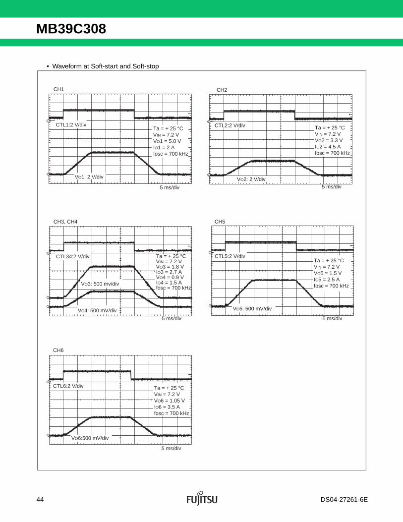
• Waveform at Soft-start and Soft-stop
Ta = + 25 °CVIN = 7.2 VVO1 = 5.0 VIO1 = 2 Afosc = 700 kHz
VO1: 2 V/div
CH1
5 ms/div
CTL1:2 V/div1
2
Ta = + 25 °CVIN = 7.2 VVO2 = 3.3 VIO2 = 4.5 Afosc = 700 kHz
CH2
CTL2:2 V/div
VO2: 2 V/div5 ms/div
1
2
Ta = + 25 °CVIN = 7.2 VVO3 = 1.8 VIO3 = 2.7 AVO4 = 0.9 VIO4 = 1.5 A fosc = 700 kHz
CH3, CH4
VO4: 500 mV/div
VO3: 500 mv/div
CTL34:2 V/div
5 ms/div
1
3
2
Ta = + 25 °CVIN = 7.2 VVO5 = 1.5 VIO5 = 2.5 Afosc = 700 kHz
CH5
VO5: 500 mV/div
CTL5:2 V/div
5 ms/div
1
2
Ta = + 25 °CVIN = 7.2 VVO6 = 1.05 VIO6 = 3.5 Afosc = 700 kHz
CH6
VO6:500 mV/div
CTL6:2 V/div
5 ms/div
1
2
44 DS04-27261-6E
MB39C308
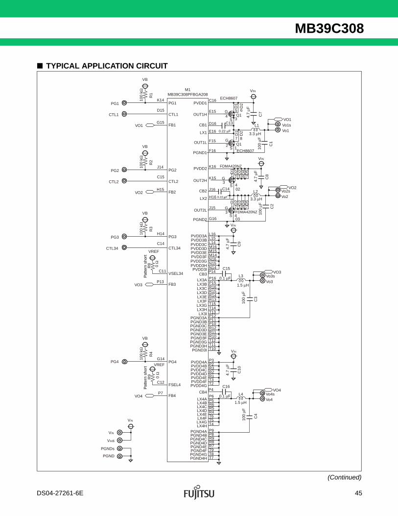
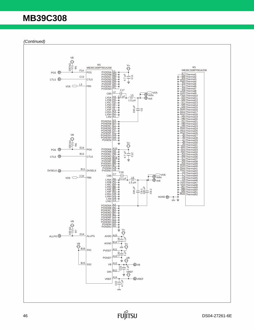
■ TYPICAL APPLICATION CIRCUIT
(Continued)
VB
M1MB39C308PFBGA208
PG1
CTL1
K14PG1 PVDD1
C16 ECH8607
VIN
VIN
C7E15
D16
E16
F15
F16
K16
K15
J16
J15
H16
G16
FDMA420NZ
FDMA420NZ
ECH8607
L16L15L14M16
C1
C2
VO1
Vo1Vo1s
VO2
Vo2Vo2s
4.7
μF
100
μF
100
μF
4.7
μF
OUT1H
CB1
LX1
OUT1L
PGND1
PVDD2
OUT2H
OUT2L
PVDD3APVDD3BPVDD3CPVDD3DPVDD3EPVDD3FPVDD3GPVDD3HPVDD3I
CB3
LX3BLX3A
PGND3APGND3BPGND3CPGND3DPGND3EPGND3FPGND3GPGND3HPGND3I
LX3CLX3DLX3ELX3FLX3GLX3HLX3I
PGND2
CB2
LX2
C9
CTL1
FB1VO1G15
D15
R1
100
kΩVB
PG2
CTL2
J14PG2
CTL2
FB2VO2H15
C15
R2
100
kΩ
VB
VREF
VSEL34
PG3
CTL34
H14PG3
CTL34
C11
FB3VO3P13
0 Ω
C14
R3
100
kΩ
VIN
VIN
VINs
PGNDs
PGND
R8
VB
FSEL4
VREFPG4
G14PG4
C12
FB4VO4P7
0 Ω
R4
100
kΩ
R9
L2
3.3 μH
C8
VIN
C3
4
VO3
Vo3Vo3s
4.7
μF
100
μF
VIN
C10
C4
M15M14N16N15N14P14
C15
P16P15R16R15R14R13T15T14T13P12P11P10R12R11R10T12T11T10
T2T3R1R2R3P2P3PVDD4A
PVDD4BPVDD4CPVDD4DPVDD4EPVDD4FPVDD4G
LX4ALX4BLX4CLX4DLX4ELX4FLX4GLX4H
L3
1.5 μH
0.1 μF
CB4 VO4
Vo4Vo4s
P4C16
P6P5R6R5R4T6T5T4
PGND4APGND4BPGND4CPGND4DPGND4EPGND4FPGND4GPGND4H
P8P9
R9R8R7T9T8T7
L4
1.5 μH
0.1 μF
Pat
tern
sho
rtP
atte
rn s
hort
03
G3
S
D5
D2
D2
D4D1
D2
D1
D2
D1
C14
0.22 0.22 μF0.22 μF
G
024
3S
2 5 61
D1
1
7
D5
D2
D2
D4
2 5 6 7
C13 L1
3.3 μH
Q1
Q1
5
7 8
1
6G
S
S
3 4.7
μF
0.22 μF
4
G2
100
μF
DS04-27261-6E 45
MB39C308
(Continued)
VB
PG5
CTL5
F14PG5
CTL5
FB5VO5L3
C13R
5
100
kΩ M1MB39C308PFBGA208 M1
MB39C308PFBGA208
VB
DVSEL6DVSEL6
PG6
CTL6
E14PG6
CTL6
B11
FB6VO6C10
B13
R6
100
kΩ
VB
VB
SS1
ALLPGD14
ALLPG
B16
R7
100
kΩ
SS2B15
4.7
μF
VIN
C11
4.7
μF
C12
VIN
N1P1
N2N3M1M2M3L1PVDD5A
PVDD5BPVDD5CPVDD5DPVDD5EPVDD5FPVDD5GPVDD5H
CB5L2
C17VO5
Vo5Vo5s
H3H2H1J3J2J1K3K2K1
0.1 μF
100
μF
L5
E7 Thermal1Thermal2Thermal3Thermal4Thermal5Thermal6Thermal7Thermal8Thermal9Thermal10Thermal11Thermal12Thermal13Thermal14Thermal15Thermal16Thermal17Thermal18Thermal19Thermal20Thermal21Thermal22Thermal23Thermal24Thermal25Thermal26Thermal27Thermal28Thermal29Thermal30Thermal31Thermal32Thermal33Thermal34Thermal35Thermal36Thermal37Thermal38Thermal39Thermal40Thermal41Thermal42
Thermal51Thermal52
Thermal43Thermal44Thermal45Thermal46Thermal47Thermal48Thermal49Thermal50
E8E9
E10
F7F6
F8F9
F10F11
G7G6G5
G8G9
G10G11G12
H7H6H5
H8H9
H10H11H12
J7J6J5
J8J9
J10J11J12
K7K6K5
K8K9
K10K11
L7L6
L8L9
L10
M7M8M9
M10
L11
K12
C5
1.5 μHLX5ALX5BLX5CLX5DLX5ELX5FLX5GLX5HLX5I
CB6C7
C18VO6
AGND
Vo6Vo6s
A6A5A4B6B5B4C6C5C4C3
0.1 μF
100
μF
L6
C6-
110
0 μF
C6-
2
1.5 μHLX6ALX6BLX6CLX6DLX6ELX6FLX6GLX6HLX6ILX6J
A3A2B3B2B1C2C1D3D2D1
PGND6APGND6BPGND6CPGND6DPGND6EPGND6FPGND6GPGND6HPGND6IPGND6J
E3E2E1F3F2F1G3G2G1
PGND5APGND5BPGND5CPGND5DPGND5EPGND5FPGND5GPGND5HPGND5I
A10A9A8A7B10B9B8B7C9C8
PVDD6APVDD6BPVDD6CPVDD6DPVDD6EPVDD6FPVDD6GPVDD6HPVDD6IPVDD6J
VIN
A15
B14 1 μF
C19
AVDD
AGND
PVDD7
PGND7
VIN
VB
VREFDIN
VB
VREFVREF
VB
A11
A13
A12
A14
B12
1 μF
1 μF
4.7
μFC
20C
22
C21
46 DS04-27261-6E
MB39C308
■ PARTS LIST
(Continued)
Sym-bol Part name Model name Specification Package Vendor Remarks
M1 IC MB39C308 ⎯ PFBGA-208 FML ⎯
Q1 N-ch Dual MOSFET ECH8607VDS = 30 V,
ID = 5 A (Max)ECH8 SANYO
Ch1 High &
Low-side
Q2-1 N-ch MOSFET FDMA420NZVDS = 20 V,ID = 5.7 A
(Max)MLP2x2-6L
FAIR-CHILD
Ch2 High-side
Q3-1 N-ch MOSFET FDMA420NZVDS = 20 V, ID = 5.7 A
(Max)MLP2x2-6L
FAIR-CHILD
Ch2 Low-side
Q2-2 N-ch MOSFET ⎯ ⎯ SOT-6 ⎯ (Ch2 High-side)
Q3-2 N-ch MOSFET ⎯ ⎯ TSOP-6 ⎯ (Ch2 Low-side)
R1 Resistor RR0816P-104-D 100 kΩ 1608 SSM PG
R2 Resistor RR0816P-104-D 100 kΩ 1608 SSM PG
R3 Resistor RR0816P-104-D 100 kΩ 1608 SSM PG
R4 Resistor RR0816P-104-D 100 kΩ 1608 SSM PG
R5 Resistor RR0816P-104-D 100 kΩ 1608 SSM PG
R6 Resistor RR0816P-104-D 100 kΩ 1608 SSM PG
R7 Resistor RR0816P-104-D 100 kΩ 1608 SSM PG
R8 Resistor ⎯ Pattern short ⎯ ⎯ VSEL34
R9 Resistor ⎯ Pattern short ⎯ ⎯ FSEL4
C1 Ceramic Capacitor C3225JB0J107M 100 μF (6.3 V) 3225 TDK VO
C2 Ceramic Capacitor C3225JB0J107M 100 μF (6.3 V) 3225 TDK VO
C3 Ceramic Capacitor GRM31CR60G107ME39L 100 μF (4 V) 3216 MURATA VO
C4 Ceramic Capacitor GRM31CR60G107ME39L 100 μF (4 V) 3216 MURATA VO
C5 Ceramic Capacitor GRM31CR60G107ME39L 100 μF (4 V) 3216 MURATA VO
C6-1 Ceramic Capacitor GRM31CR60G107ME39L 100 μF (4 V) 3216 MURATA VO
C6-2 Ceramic Capacitor GRM31CR60G107ME39L 100 μF (4 V) 3216 MURATA VO
C7 Ceramic Capacitor C2012JB1C475K 4.7 μF (16 V) 2012 TDK PVDD
C8 Ceramic Capacitor C2012JB1C475K 4.7 μF (16 V) 2012 TDK PVDD
C9 Ceramic Capacitor C2012JB1C475K 4.7 μF (16 V) 2012 TDK PVDD
C10 Ceramic Capacitor C2012JB1C475K 4.7 μF (16 V) 2012 TDK PVDD
C11 Ceramic Capacitor C2012JB1C475K 4.7 μF (16 V) 2012 TDK PVDD
C12 Ceramic Capacitor C2012JB1C475K 4.7 μF (16 V) 2012 TDK PVDD
DS04-27261-6E 47
MB39C308
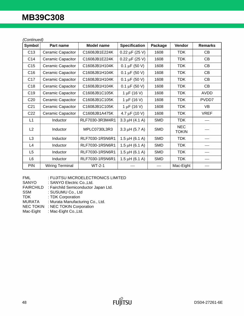
(Continued)
FML : FUJITSU MICROELECTRONICS LIMITEDSANYO : SANYO Electric Co.,Ltd.FAIRCHILD : Fairchild Semiconductor Japan Ltd.SSM : SUSUMU Co., LtdTDK : TDK CorporationMURATA : Murata Manufacturing Co., Ltd.NEC TOKIN : NEC TOKIN CorporationMac-Eight : Mac-Eight Co.,Ltd.
Symbol Part name Model name Specification Package Vendor Remarks
C13 Ceramic Capacitor C1608JB1E224K 0.22 μF (25 V) 1608 TDK CB
C14 Ceramic Capacitor C1608JB1E224K 0.22 μF (25 V) 1608 TDK CB
C15 Ceramic Capacitor C1608JB1H104K 0.1 μF (50 V) 1608 TDK CB
C16 Ceramic Capacitor C1608JB1H104K 0.1 μF (50 V) 1608 TDK CB
C17 Ceramic Capacitor C1608JB1H104K 0.1 μF (50 V) 1608 TDK CB
C18 Ceramic Capacitor C1608JB1H104K 0.1 μF (50 V) 1608 TDK CB
C19 Ceramic Capacitor C1608JB1C105K 1 μF (16 V) 1608 TDK AVDD
C20 Ceramic Capacitor C1608JB1C105K 1 μF (16 V) 1608 TDK PVDD7
C21 Ceramic Capacitor C1608JB1C105K 1 μF (16 V) 1608 TDK VB
C22 Ceramic Capacitor C1608JB1A475K 4.7 μF (10 V) 1608 TDK VREF
L1 Inductor RLF7030-3R3M4R1 3.3 μH (4.1 A) SMD TDK ⎯
L2 Inductor MPLC0730L3R3 3.3 μH (5.7 A) SMDNEC
TOKIN⎯
L3 Inductor RLF7030-1R5N6R1 1.5 μH (6.1 A) SMD TDK ⎯
L4 Inductor RLF7030-1R5N6R1 1.5 μH (6.1 A) SMD TDK ⎯
L5 Inductor RLF7030-1R5N6R1 1.5 μH (6.1 A) SMD TDK ⎯
L6 Inductor RLF7030-1R5N6R1 1.5 μH (6.1 A) SMD TDK ⎯
PIN Wiring Terminal WT-2-1 ⎯ ⎯ Mac-Eight ⎯
48 DS04-27261-6E
MB39C308
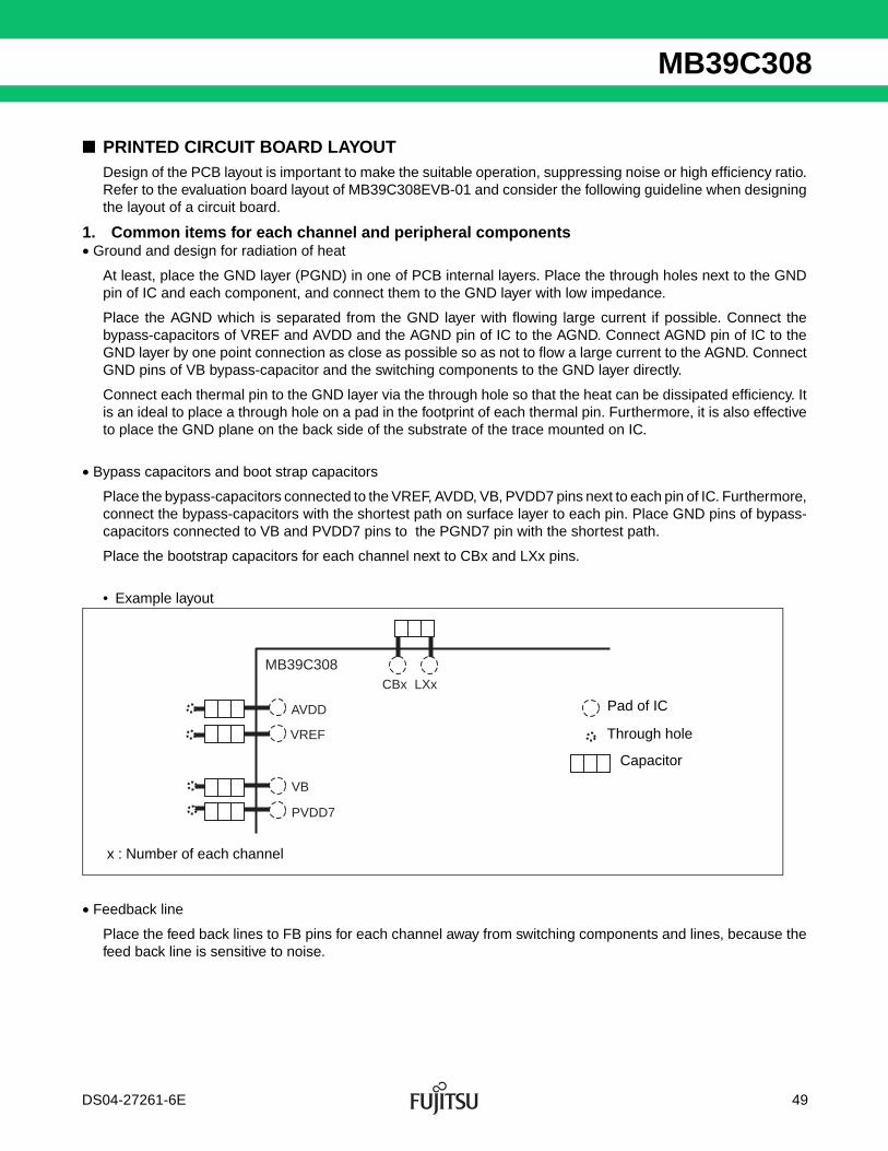
■ PRINTED CIRCUIT BOARD LAYOUTDesign of the PCB layout is important to make the suitable operation, suppressing noise or high efficiency ratio.Refer to the evaluation board layout of MB39C308EVB-01 and consider the following guideline when designingthe layout of a circuit board.
1. Common items for each channel and peripheral components • Ground and design for radiation of heat
At least, place the GND layer (PGND) in one of PCB internal layers. Place the through holes next to the GNDpin of IC and each component, and connect them to the GND layer with low impedance.
Place the AGND which is separated from the GND layer with flowing large current if possible. Connect thebypass-capacitors of VREF and AVDD and the AGND pin of IC to the AGND. Connect AGND pin of IC to theGND layer by one point connection as close as possible so as not to flow a large current to the AGND. ConnectGND pins of VB bypass-capacitor and the switching components to the GND layer directly.
Connect each thermal pin to the GND layer via the through hole so that the heat can be dissipated efficiency. Itis an ideal to place a through hole on a pad in the footprint of each thermal pin. Furthermore, it is also effectiveto place the GND plane on the back side of the substrate of the trace mounted on IC.
• Bypass capacitors and boot strap capacitors
Place the bypass-capacitors connected to the VREF, AVDD, VB, PVDD7 pins next to each pin of IC. Furthermore,connect the bypass-capacitors with the shortest path on surface layer to each pin. Place GND pins of bypass-capacitors connected to VB and PVDD7 pins to the PGND7 pin with the shortest path.
Place the bootstrap capacitors for each channel next to CBx and LXx pins.
• Example layout
• Feedback line
Place the feed back lines to FB pins for each channel away from switching components and lines, because thefeed back line is sensitive to noise.
MB39C308
VREF
AVDD
VB
PVDD7
LXxCBx
Capacitor
x : Number of each channel
Through hole
Pad of IC
DS04-27261-6E 49
MB39C308
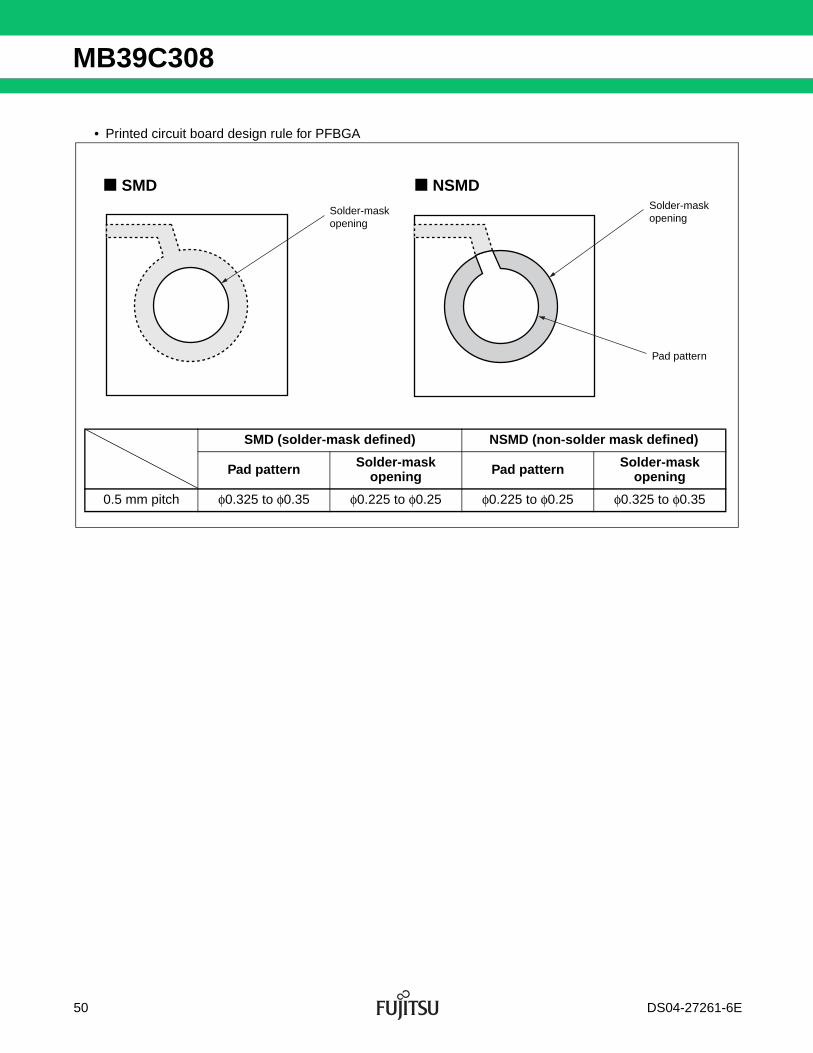
• Printed circuit board design rule for PFBGA
SMD (solder-mask defined) NSMD (non-solder mask defined)
Pad pattern Solder-mask opening Pad pattern Solder-mask
opening
0.5 mm pitch φ0.325 to φ0.35 φ0.225 to φ0.25 φ0.225 to φ0.25 φ0.325 to φ0.35
Solder-maskopening
Solder-maskopening
Pad pattern
■ SMD ■ NSMD
50 DS04-27261-6E
MB39C308
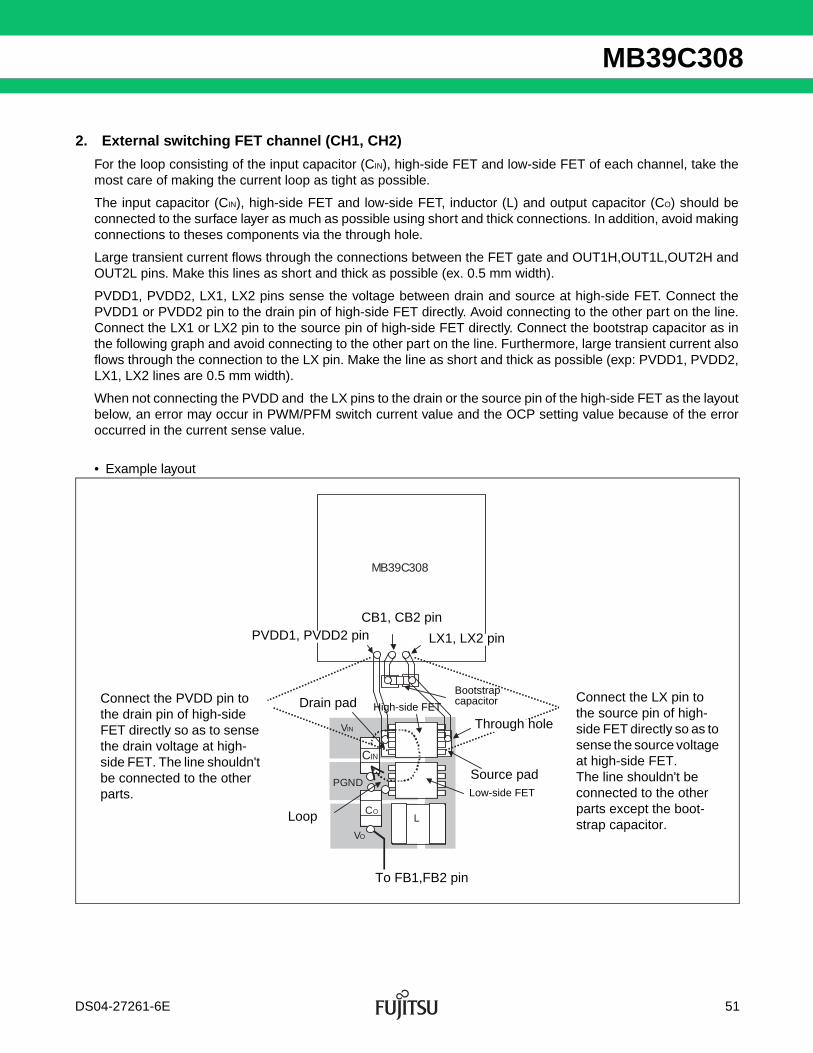
2. External switching FET channel (CH1, CH2)
For the loop consisting of the input capacitor (CIN), high-side FET and low-side FET of each channel, take themost care of making the current loop as tight as possible.
The input capacitor (CIN), high-side FET and low-side FET, inductor (L) and output capacitor (CO) should beconnected to the surface layer as much as possible using short and thick connections. In addition, avoid makingconnections to theses components via the through hole.
Large transient current flows through the connections between the FET gate and OUT1H,OUT1L,OUT2H andOUT2L pins. Make this lines as short and thick as possible (ex. 0.5 mm width).
PVDD1, PVDD2, LX1, LX2 pins sense the voltage between drain and source at high-side FET. Connect thePVDD1 or PVDD2 pin to the drain pin of high-side FET directly. Avoid connecting to the other part on the line.Connect the LX1 or LX2 pin to the source pin of high-side FET directly. Connect the bootstrap capacitor as inthe following graph and avoid connecting to the other part on the line. Furthermore, large transient current alsoflows through the connection to the LX pin. Make the line as short and thick as possible (exp: PVDD1, PVDD2,LX1, LX2 lines are 0.5 mm width).
When not connecting the PVDD and the LX pins to the drain or the source pin of the high-side FET as the layoutbelow, an error may occur in PWM/PFM switch current value and the OCP setting value because of the erroroccurred in the current sense value.
• Example layout
VIN
CIN
COL
PGND
VO
MB39C308
PVDD1, PVDD2 pin
Through hole
Low-side FET
To FB1,FB2 pin
Bootstrap capacitor Connect the LX pin to
the source pin of high-side FET directly so as to sense the source voltage at high-side FET. The line shouldn't be connected to the other parts except the boot-strap capacitor.
Connect the PVDD pin to the drain pin of high-side FET directly so as to sense the drain voltage at high-side FET. The line shouldn't be connected to the other parts.
CB1, CB2 pin
LX1, LX2 pin
High-side FETDrain pad
Source pad
Loop
DS04-27261-6E 51
MB39C308
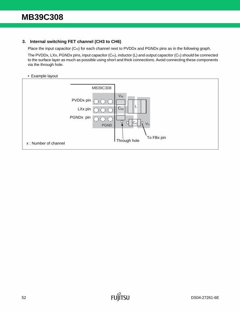
3. Internal switching FET channel (CH3 to CH6)
Place the input capacitor (CIN) for each channel next to PVDDx and PGNDx pins as in the following graph.
The PVDDx, LXx, PGNDx pins, input capacitor (CIN), inductor (L) and output capacitor (CO) should be connectedto the surface layer as much as possible using short and thick connections. Avoid connecting these componentsvia the through hole.
• Example layout
VIN
PGND
CIN
MB39C308
CO
L
VO
To FBx pin
x : Number of channel
PVDDx pin
Through hole
LXx pin
PGNDx pin
52 DS04-27261-6E
MB39C308
■ USAGE PRECAUTION1. Do not configure the IC over the maximum ratings
lf the lC is used over the maximum ratings, the LSl may be permanently damaged.It is preferable for the device to normally operate within the recommended usage conditions. Usage outside ofthese conditions can have a bad effect on the reliability of the LSI.
2. Use the devices within recommended operating conditions
The recommended operating conditions are under which the LSl is guaranteed to operate. The electrical ratings are guaranteed when the device is used within the recommended operating conditionsand under the conditions stated for each item.
3. Printed circuit board ground lines should be set up with consideration for common impedance
4. Take appropriate measures against static electricity• Containers for semiconductor materials should have anti-static protection or be made of conductive material.• After mounting, printed circuit boards should be stored and shipped in conductive bags or containers.• Work platforms, tools, and instruments should be properly grounded.• Working personnel should be grounded with resistance of 250 kΩ to 1 MΩ between body and ground.
5. Do not apply negative voltagesThe use of negative voltages below –0.3 V may create parasitic transistors on LSI lines, which can cause malfunctions.
6. Warnings when connecting the load
During DC/DC operation, if the output is connected by hard switching to a capacitance that greatly exceeds theDC/DC output capacitance, the output voltage may oscillate and the protection function may be detected dueto the instant voltage drop. Take note of the following points.
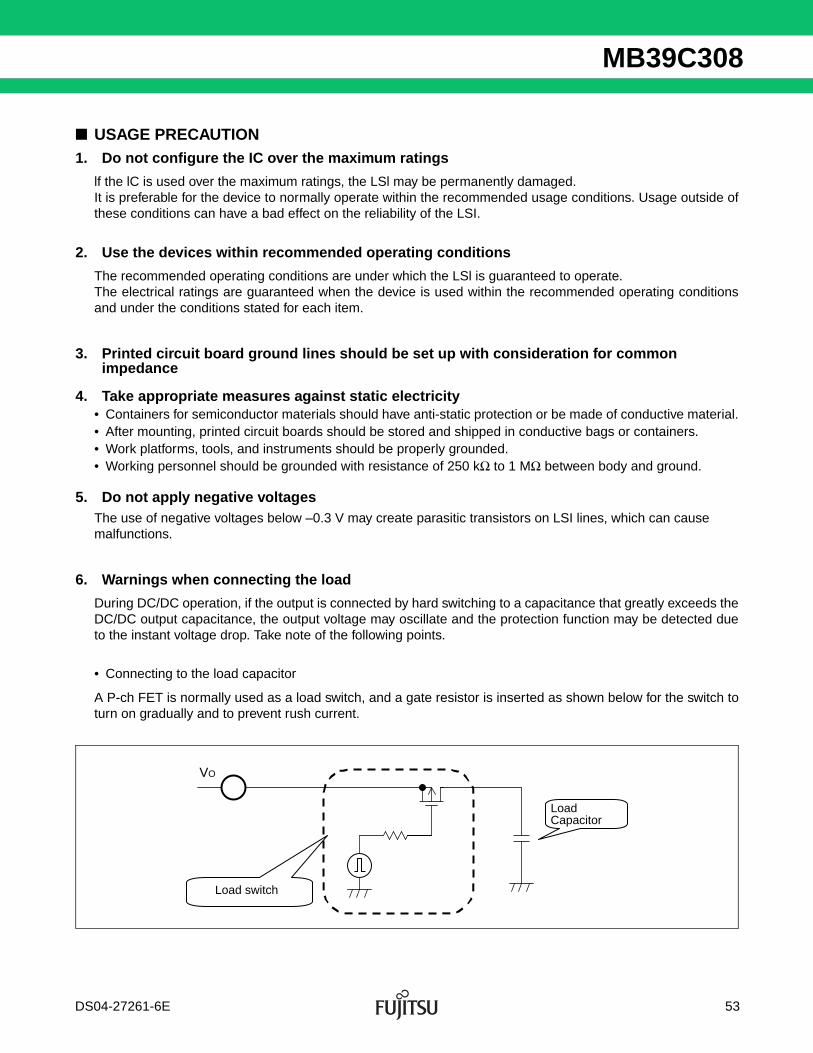
• Connecting to the load capacitor
A P-ch FET is normally used as a load switch, and a gate resistor is inserted as shown below for the switch toturn on gradually and to prevent rush current.
VO
Load switch
Load Capacitor
DS04-27261-6E 53
MB39C308
7. Partial short circuits
Normally, in the event of a short circuit, such as the DC/DC output connecting to ground or low potential point,output is stopped by the short circuit protection (SCP) function. Take care in the event of a partial short circuit,because the output is not stopped by the short circuit protection (SCP) function. It is recommended that a fusebe inserted into the input. If the short circuit conditions partially occur in several channels which contain the FET,there is a possibility of smoke or fire. [Partial short circuit : Refers to a short circuit condition where overcurrent flows but is not strong enough todecrease the output voltage.]
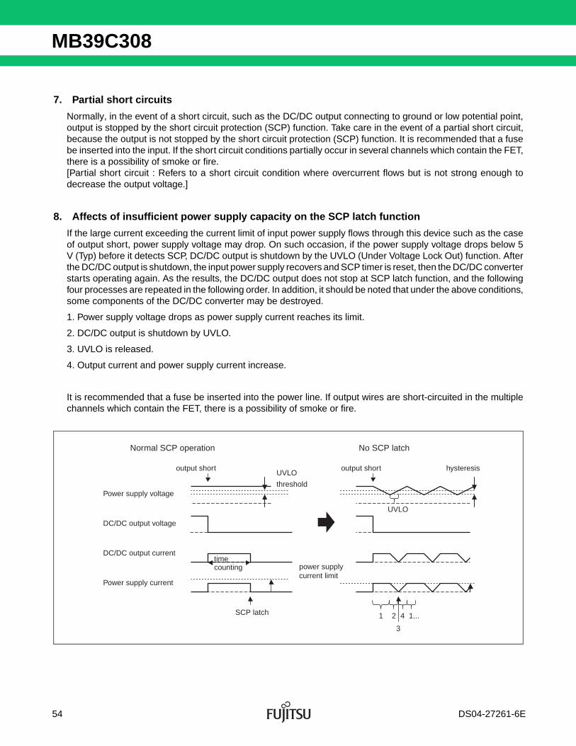
8. Affects of insufficient power supply capacity on the SCP latch function
If the large current exceeding the current limit of input power supply flows through this device such as the caseof output short, power supply voltage may drop. On such occasion, if the power supply voltage drops below 5V (Typ) before it detects SCP, DC/DC output is shutdown by the UVLO (Under Voltage Lock Out) function. Afterthe DC/DC output is shutdown, the input power supply recovers and SCP timer is reset, then the DC/DC converterstarts operating again. As the results, the DC/DC output does not stop at SCP latch function, and the followingfour processes are repeated in the following order. In addition, it should be noted that under the above conditions,some components of the DC/DC converter may be destroyed.
1. Power supply voltage drops as power supply current reaches its limit.
2. DC/DC output is shutdown by UVLO.
3. UVLO is released.
4. Output current and power supply current increase.
It is recommended that a fuse be inserted into the power line. If output wires are short-circuited in the multiplechannels which contain the FET, there is a possibility of smoke or fire.
DC/DC output voltage
DC/DC output current
Power supply voltage
output short
Normal SCP operation
Power supply current
3
power supply current limit
41 2 1...
UVLO
threshold
No SCP latch
SCP latch
UVLO
timecounting
output short hysteresis
54 DS04-27261-6E
MB39C308
■ ORDERING INFORMATION
■ EV BOARD ORDERING INFORMATION
■ RoHS COMPLIANCE INFORMATION OF LEAD (Pb) FREE VERSIONThe LSI products of Fujitsu Microelectronics with “E1” are compliant with RoHS Directive , and has observedthe standard of lead, cadmium, mercury, hexavalent chromium, polybrominated biphenyls (PBB) , and polybro-minated diphenyl ethers (PBDE) .
A product whose part number has trailing characters “E1” is RoHS compliant.
■ MARKING FORMAT (LEAD FREE VERSION)
Part number Package Remarks
MB39C308BGF208-ball plastic PFBGA
(BGA-208P-M02)
EV board part No. EV board version No. Remarks
MB39C308EVB-11 Board rev.1.0 PFBGA-208
INDEX
MXXXX
E 1
J
XXXB 39C308
APAN
Lead-free version
DS04-27261-6E 55
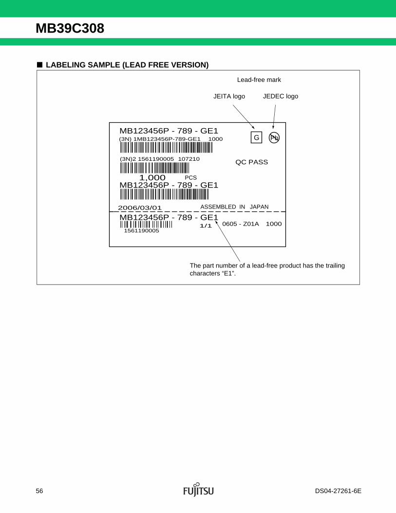
MB39C308
■ LABELING SAMPLE (LEAD FREE VERSION)
2006/03/01 ASSEMBLED IN JAPAN
G
QC PASS
(3N) 1MB123456P-789-GE1 1000
(3N)2 1561190005 107210
1,000 PCS
0605 - Z01A 10001/11561190005
MB123456P - 789 - GE1
MB123456P - 789 - GE1
MB123456P - 789 - GE1
Pb
Lead-free mark
JEITA logo JEDEC logo
The part number of a lead-free product has the trailing characters “E1”.
56 DS04-27261-6E
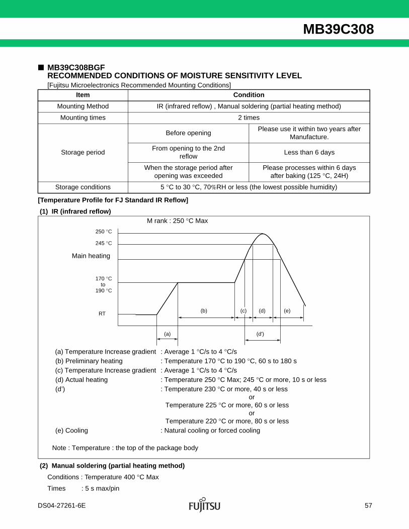
MB39C308
■ MB39C308BGF RECOMMENDED CONDITIONS OF MOISTURE SENSITIVITY LEVEL[Fujitsu Microelectronics Recommended Mounting Conditions]
[Temperature Profile for FJ Standard IR Reflow]
(1) IR (infrared reflow)
(2) Manual soldering (partial heating method)
Conditions : Temperature 400 °C Max
Times : 5 s max/pin
Item Condition
Mounting Method IR (infrared reflow) , Manual soldering (partial heating method)
Mounting times 2 times
Storage period
Before opening Please use it within two years after
Manufacture.
From opening to the 2ndreflow
Less than 6 days
When the storage period afteropening was exceeded
Please processes within 6 daysafter baking (125 °C, 24H)
Storage conditions 5 °C to 30 °C, 70%RH or less (the lowest possible humidity)
250 °C
(e)
(d')
(d)
245 °C
170 °C
190 °C
RT (b)
(a)
(c)
to
Note : Temperature : the top of the package body
(a) Temperature Increase gradient : Average 1 °C/s to 4 °C/s (b) Preliminary heating : Temperature 170 °C to 190 °C, 60 s to 180 s (c) Temperature Increase gradient : Average 1 °C/s to 4 °C/s (d) Actual heating : Temperature 250 °C Max; 245 °C or more, 10 s or less (d’) : Temperature 230 °C or more, 40 s or less
orTemperature 225 °C or more, 60 s or less
orTemperature 220 °C or more, 80 s or less
(e) Cooling : Natural cooling or forced cooling
M rank : 250 °C Max
Main heating
DS04-27261-6E 57
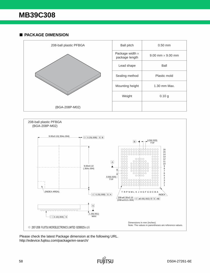
MB39C308
■ PACKAGE DIMENSION
Please check the latest Package dimension at the following URL.http://edevice.fujitsu.com/package/en-search/
208-ball plastic PFBGA Ball pitch 0.50 mm
Package width ×package length
9.00 mm × 9.00 mm
Lead shape Ball
Sealing method Plastic mold
Mounting height 1.30 mm Max.
Weight 0.10 g
208-ball plastic PFBGA(BGA-208P-M02)
(BGA-208P-M02)
C 2007-2008 FUJITSU MICROELECTRONICS LIMITED B208002S-c-1-5
9.00±0.10(.354±.004)
0.50(.020)TYP
T R P N M L K J H G F E D C B A
16151413121110987654321
0.20(.008) BS
0.20(.008) AS
9.00±0.10(.354±.004)
(INDEX AREA)
0.10(.004) S MAX
S
1.30(.051)
INDEX
(208-ø.012±.004)208-ø0.30±0.10
M S ABø0.05(.002)
B
0.50(.020)TYP
A
Dimensions in mm (inches).Note: The values in parentheses are reference values.
58 DS04-27261-6E
MB39C308
■ CONTENTSpage
- DESCRIPTION .................................................................................................................................................... 1- FEATURES .......................................................................................................................................................... 1- APPLICATIONS .................................................................................................................................................. 2- PIN ASSIGNMENT ............................................................................................................................................. 3- PIN DESCRIPTIONS .......................................................................................................................................... 4- BLOCK DIAGRAM .............................................................................................................................................. 7- ABSOLUTE MAXIMUM RATINGS ................................................................................................................... 9- RECOMMENDED OPERATING CONDITIONS ............................................................................................ 10- ELECTRICAL CHARACTERISTICS ................................................................................................................ 12- CHANNEL CONTROL FUNCTION .................................................................................................................. 19- POWER GOOD FUNCTION ............................................................................................................................. 19- PROTECTION ..................................................................................................................................................... 20- DESCRIPTION OF SOFT-START AND SOFT-STOP OPERATION ......................................................... 21- PRESET FUNCTION OF CH3/CH4/CH6 OUTPUT VOLTAGE .................................................................. 23- TYPICAL CHARACTERISTICS ........................................................................................................................ 24- NOTES FOR UNCONNECTED PINS ............................................................................................................. 26- APPLICATION NOTE ......................................................................................................................................... 30- REFERENCE DATA ........................................................................................................................................... 37- TYPICAL APPLICATION CIRCUIT .................................................................................................................. 45- PARTS LIST ......................................................................................................................................................... 47- PRINTED CIRCUIT BOARD LAYOUT ............................................................................................................ 49- USAGE PRECAUTION ...................................................................................................................................... 53- ORDERING INFORMATION ............................................................................................................................. 55- EV BOARD ORDERING INFORMATION ....................................................................................................... 55- RoHS COMPLIANCE INFORMATION OF LEAD (Pb) FREE VERSION .................................................. 55- MARKING FORMAT (LEAD FREE VERSION) .............................................................................................. 55- LABELING SAMPLE (LEAD FREE VERSION) ............................................................................................. 56- MB39C308BGF RECOMMENDED CONDITIONS OF MOISTURE SENSITIVITY LEVEL .................... 57- PACKAGE DIMENSION .................................................................................................................................... 58
DS04-27261-6E 59

MB39C308
FUJITSU MICROELECTRONICS LIMITEDShinjuku Dai-Ichi Seimei Bldg., 7-1, Nishishinjuku 2-chome,Shinjuku-ku, Tokyo 163-0722, JapanTel: +81-3-5322-3329http://jp.fujitsu.com/fml/en/
For further information please contact:
North and South AmericaFUJITSU MICROELECTRONICS AMERICA, INC.1250 E. Arques Avenue, M/S 333Sunnyvale, CA 94085-5401, U.S.A.Tel: +1-408-737-5600 Fax: +1-408-737-5999http://www.fma.fujitsu.com/
EuropeFUJITSU MICROELECTRONICS EUROPE GmbHPittlerstrasse 47, 63225 Langen, GermanyTel: +49-6103-690-0 Fax: +49-6103-690-122http://emea.fujitsu.com/microelectronics/
KoreaFUJITSU MICROELECTRONICS KOREA LTD.206 Kosmo Tower Building, 1002 Daechi-Dong,Gangnam-Gu, Seoul 135-280, Republic of KoreaTel: +82-2-3484-7100 Fax: +82-2-3484-7111http://kr.fujitsu.com/fmk/
Asia PacificFUJITSU MICROELECTRONICS ASIA PTE. LTD.151 Lorong Chuan,#05-08 New Tech Park 556741 SingaporeTel : +65-6281-0770 Fax : +65-6281-0220http://www.fmal.fujitsu.com/
FUJITSU MICROELECTRONICS SHANGHAI CO., LTD.Rm. 3102, Bund Center, No.222 Yan An Road (E),Shanghai 200002, ChinaTel : +86-21-6146-3688 Fax : +86-21-6335-1605http://cn.fujitsu.com/fmc/
FUJITSU MICROELECTRONICS PACIFIC ASIA LTD.10/F., World Commerce Centre, 11 Canton Road,Tsimshatsui, Kowloon, Hong KongTel : +852-2377-0226 Fax : +852-2376-3269http://cn.fujitsu.com/fmc/en/
Specifications are subject to change without notice. For further information please contact each office.
All Rights Reserved.The contents of this document are subject to change without notice. Customers are advised to consult with sales representatives before ordering.The information, such as descriptions of function and application circuit examples, in this document are presented solely for the purposeof reference to show examples of operations and uses of FUJITSU MICROELECTRONICS device; FUJITSU MICROELECTRONICSdoes not warrant proper operation of the device with respect to use based on such information. When you develop equipment incorporatingthe device based on such information, you must assume any responsibility arising out of such use of the information. FUJITSU MICROELECTRONICS assumes no liability for any damages whatsoever arising out of the use of the information.Any information in this document, including descriptions of function and schematic diagrams, shall not be construed as license of the useor exercise of any intellectual property right, such as patent right or copyright, or any other right of FUJITSU MICROELECTRONICSor any third party or does FUJITSU MICROELECTRONICS warrant non-infringement of any third-party's intellectual property right orother right by using such information. FUJITSU MICROELECTRONICS assumes no liability for any infringement of the intellectualproperty rights or other rights of third parties which would result from the use of information contained herein.The products described in this document are designed, developed and manufactured as contemplated for general use, including withoutlimitation, ordinary industrial use, general office use, personal use, and household use, but are not designed, developed and manufacturedas contemplated (1) for use accompanying fatal risks or dangers that, unless extremely high safety is secured, could have a serious effect tothe public, and could lead directly to death, personal injury, severe physical damage or other loss (i.e., nuclear reaction control in nuclearfacility, aircraft flight control, air traffic control, mass transport control, medical life support system, missile launch control in weaponsystem), or (2) for use requiring extremely high reliability (i.e., submersible repeater and artificial satellite).Please note that FUJITSU MICROELECTRONICS will not be liable against you and/or any third party for any claims or damages arisingin connection with above-mentioned uses of the products.Any semiconductor devices have an inherent chance of failure. You must protect against injury, damage or loss from such failures byincorporating safety design measures into your facility and equipment such as redundancy, fire protection, and prevention of over-currentlevels and other abnormal operating conditions.Exportation/release of any products described in this document may require necessary procedures in accordance with the regulations ofthe Foreign Exchange and Foreign Trade Control Law of Japan and/or US export control laws.The company names and brand names herein are the trademarks or registered trademarks of their respective owners.
Edited: Sales Promotion Department