Embed Size (px)
Citation preview

THE EFFECT OF ETCH FACTOR ON PRINTED WIRING CHARACTERISTIC IMPEDANCE
ABSTRACT
As logic switching speeds continue to increase, signal integrity becomes increasinglyimportant. The signal paths have to be treated as transmission lines to accuratelypredict signal integrity. Many software tools exist to calculate transmission linecharacteristic impedance of printed-wiring traces as part of the overall signal analysis.
As the logic speeds get even faster, the effect of transmission line mismatch becomesmore serious. Many of the software tools assume a rectangular cross-section for thetraces. In actuality, the trace cross-sections more closely approximate a trapezoid dueto the etching process.
We have used a field modeling program to determine the characteristic impedance ofa variety of traces including buried microstrip, symmetrical stripline, edge-coupledpair, and broadside-coupled pair. These impedance determinations were performedwith both rectangular and trapezoidal cross sections. In some cases, the difference incharacteristic impedance between rectangular and trapezoidal cross-sections exceededsix percent.
Wednesday, October 3, 2001
11th ANNUAL REGIONAL SYMPOSIUM ON ELECTROMAGNETIC COMPATIBILITY
Rocky Mountain Chapter of the IEEE EMC Society at the Radisson Inn, Northglenn, Colorado.
Steve Monroe tto BuhlerStorage Technology Corporation Storage Technology CorporationMS 2201 MS 4274One StorageTek Drive One StorageTek DriveLouisville, Colorado 80028-2201 Louisville, Colorado 80028-4274(303) 673-4938 (303) [email protected] [email protected]

CONTENTS _
Introduction ................................................................................................................... 3
Lumped Circuit Analysis .............................................................................................. 3
Transmission Line Basics .............................................................................................. 5
Transmission Line Analysis .......................................................................................... 8
Etch Factor ...................................................................................................................... 9 Buried Microstrip .................................................................................... 10 Symmetrical Stripline ............................................................................. 15 Edge-Coupled Pair .................................................................................. 17 Surface Microstrip ........................................................................ 19 Broadside-Coupled Pair .......................................................................... 21
Field Modeling Tools ..................................................................................................... 23
Conclusions ..................................................................................................................... 24
References ....................................................................................................................... 25
Appendix ......................................................................................................................... 26 Transmission Line Crib Sheet
Page 2

Introduction: The edge rate of digital signals on printed wiring boards continues toincrease. For reliable operation we have to pay attention to signal integrity. For slowsignals (edge rates) we could use lumped (or discrete) circuit analysis techniques topredict signal behavior. At faster edge rates we have to switch to distributed circuitanalysis techniques to accurately predict signal behavior. This takes the form oftransmission line analysis. We will quickly review the older lumped circuit analysis andsee where it is no longer valid. A review of transmission lines will follow including adiscussion of characteristic impedance and signal reflections. From there we will discussetch factor; what it is and how it affects characteristic impedance. From there we willpresent the results of electromagnetic field simulations to determine the characteristicimpedance of printed wiring traces with different etch factors.
Lumped Circuit Analysis: An example of a signal path suitable for lumped circuitanalysis is shown in Figure 1.
10 inch
200 Ω
C = 3.30 pF/inch L = 8.70 nH/inch Z0 = 51.3 Ω tpd = 170 ps/inch
FIGURE 1: Digital Signal Path With Salient Parameters
Assuming really old technology, the output inherent rise time (i.e. unloaded output) ofthe driver is 12 ns. Note that the buffer propagation delay does not enter in here. It isonly the rise time we are interested in.
The signal delay from the transmitter output to receiver input will be: [path length (in inches)] [path delay (in ps/inch)] = [10 inch][170 ps/inch] = 1.7 ns.
Pages 7 and 8 of Reference 1 give a criteria for lumped versus transmission lineanalysis. If the signal rise time is greater than six times the path delay, lumped analysisshould suffice. If the signal rise time is less than six times the path delay, transmissionline analysis is required. In our example 12 ns > 6(1.7 ns) = 10.2 ns. Lumped analysisshould be sufficient.
Page 3

Assuming a high impedance receiver, we ignore the path inductance and concentrateon path capacitance: Cpath = (10 inch)(3.3 pF/inch) = 33 pF. We will slightly simplifythe analysis by ignoring the input capacitance of the receiver and the output capacitanceof the driver.
The output driver 10 – 90 % rise time due to capacitive output loading is 2.2 RC timeconstants = 2.2(200 Ω)(33 pF) = 14.5 ns. The total output rise time can be approximatedby the square root of the sum of the squares of the individual contributors. In this case:
Tr-total = Tr12 + Tr2
2 = (12 ns)2 + (14.5)2 = 18.8 ns
We paid attention to C and tpd, and ignored L and Z0. Z0 is the characteristicimpedance of the transmission line and will be considered in the next section.
Transmission Line Basics: If we “soup up” the driver in Figure 1 by decreasing theoutput resistance to 20 Ω and assume an inherent rise time of 0.5 ns without externalloading we will have to use transmission line analysis for valid analysis. Lets look first attransmission line basics and then apply it to the souped up driver. A typical transmissionline for logic circuits is the microstrip shown in figure 2. It is a conductive trace inproximity to a signal return plane (ground or power).
Signal Trace
Dielectric (∈r) Signal return plane (ground)
FIGURE 2: Microstrip Structure
The structure shown in Figure 2 is a surface microstrip. Had the signal trace beentotally encased in dielectric it would be a buried microstrip. There are four stray effectsto consider with this structure. There is resistance associated with the signal trace. Thelonger the trace, the greater the resistance. Likewise, there is inductance associated withthe signal trace. The longer the trace, the greater the inductance. We can represent thesetwo quantities as a series RL circuit. There is also capacitance from the signal trace toground and a low conductance (high leakage) from trace to ground. Pulling this
Page 4
altogether, we have the lossy transmission line equivalent circuit of Figure 3.
R L
C G
FIGURE 3: Lossy Transmission Line Section
Figure 3 depicts a distributed circuit (transmission line) as a lumped circuit equivalent.The accuracy of the model depends on how fine we make it. As an example, considerour ten inch trace from Figure 1. We could model that whole line with a single sectionwith L = 87 nH and C = 33 pF. However, given a total section delay of 1.7 ns we canassume that the model is valid only for rise times greater than (6)(1.7 ns) or 10.2 ns. Ifwe want the model to be accurate for 0.5 ns rise times, each section should have a delayless than (0.5 ns)/6 = 83.3 ps. This implies we should have a minimum of :(1.7 ns)/(83.3 ps/section) = 20.4 sections. Rounding up to 21 sections we would modelthe line as a cascade of 21 identical sections. Each section would have L = (87 nH)/21 =4.14 nH and C = (3.3 pF)/21 = 0.157 pF. The delay per section is then (1700 ps)/21 =81.0 ps. In like manner, the total resistance of the line would be divided by 21 to get anequivalent R per section as would the total G also be divided by 21.
We can consider the line section to have a series impedance Z = R + jωL where ω is(2π)(operating frequency). In like manner, the line section also has a shunt admittanceY = G + jωC. The characteristic impedance is given by: Z0 = (Z/Y)1/2. A discussion ofcharacteristic impedance will follow shortly.
For most transmission lines; the capacitance is relatively constant with frequency,R above a certain frequency tends to increase as the square root of frequency, G increaseswith frequency, and L will change somewhat from a low frequency value to a lower valueinductance at higher frequencies. The L and R variation with frequency is due to skineffect. More discussion on L and R can be found in Reference 2.
In many applications, the transmission line losses are relatively low which allows us tosimplify the circuit of Figure 3. Generally, G does not affect us much until we are in theGHz range. Also, in many cases R is low enough that we can neglect it. This leaves asimpler transmission line section consisting only of L and C. This is the lossless line.Some useful transmission line approximations for the lossless line can be found in theappendix. Page 5

The lossless line allows us an easy way to visualize characteristic impedance.Consider the infinite-lossless transmission line in Figure 4.
t = 0
i
E E/Z0
i
0
0 t
FIGURE 4: Infinite-Lossless Transmission Line
For the infinite- lossless line, the current remains constant with time. Each sectioncharges up only to have the next section begin charging and drawing current. Thecurrent-voltage relationship appears to be that of a resistor. The characteristic impedanceis the value of that apparent resistance. For the lossless line, the equation forcharacteristic impedance reduces to: Z0 = L/C
Consider the transmission line in Figure 5 driving a load ZL.
Incident Wave Z0 Reflected Wave
RL
FIGURE 5: Transmission Line Driving a Load (ZL = RL)
In Figure 5 if Z0 = ZL, the incident wave that arrives at the end of the line is absorbedby the load and there is no reflection. If the load is not matched to the line, some of theenergy will be reflected back as indicated by a reflected wave. The amount of reflectionis given by:
Page 6

ρρ = ZL – Z0 _ Where: ρ = the reflection coefficient ( -1.0 ≤ ρ ≤ +1.0 )
ZL + Z0 Z0 = transmission line characteristic impedance ZL = load impedance
Example: If Z0 = 50 Ω, ZL = 40 Ω, and the incident wave is a 5 volt step:ρ = (40 – 50)/(40 + 50) = -0.1111 which implies that 11.11 % of the incident wave isreflected back in the opposite polarity. (5V)(-0.1111) = -0.5555 volt reflected ⇒ wewill have a net signal of 5 V – 0.5555 V = 4.4445 V at time of reflection.
Example: If Z0 = 50 Ω, ZL = 60 Ω, and the incident wave is a 5 volt step:ρ = (60 – 50)/(60 + 50) = +0.0909 which implies that 9.09 % of the incident wave isreflected back in the same polarity. (5V)(0.0909) = +0.4545 volt reflected ⇒ we willhave a net signal of 5 V + 0.4545 V at time of reflection.
For gross estimates we can approximate the reflection coefficient as being half themismatch: ZL/Z0_ Mismatch_ Mismatch/2 ρ _ 1.2 0.2 0.1 0.0909 0.8 - 0.2 - 0.1 - 0.1111 1.05 0.05 0.025 0.0243 0.95 - 0.05 - 0.025 - 0.0256
Referring to Figure 2 and taking on one other piece of information, we can get a goodfeel for what happens when we change the physical dimensions of the signal trace. For agiven dielectric constant, the propagation velocity (vp) of a lossless line is independent ofthe conductor dimensions. For a buried microstrip with thick dielectric, the effectivedielectric constant (∈r-eff) is equal to the material dielectric constant (∈r). For a surfacemicrostrip as shown in Figure 2, ∈r-eff < ∈r. In either case, the propagation velocity isgiven by: vp = c ∈∈r-eff Where c = speed of light in vacuum c = 299,792,458 m/s ≈ 11.80 inch/ns
Propagation delay is the reciprocal of propagation velocity. In vacuum, propagationdelay is 84.723 ps/inch. Thus, in general tpd = (84.723 ps/inch)(∈r-eff)
1/2.
The propagation delay may also be found if L and C are known: tpd = LC .Intuitively, we know the direction C will take for dimensional changes even though wemay not know the amount. Whatever amount C changes, L will have to change by thesame amount in the opposite direction in order to keep tpd constant. Thus we can createthe table on the next page with W = conductor width, H = conductor height above theground plane, and T = conductor thickness. An upward arrow signifies an increase, adownward arrow signifies a decrease, and a dash signifies no change. It should be notedthat this table is for high frequencies or the lossless case.
Page 7

_ W H T C L Z0 = (L/C)1/2 _ ↑ ↑ ↓ ↓
↑ ↓ ↑ ↑
↑ ↑ ↓ ↓ _ _
While we were able to qualitatively figure out the electrical effect of dimensionalchanges in the microstrip, getting quantitative results is much more difficult. Looking atthe electric field of the microstrip as shown in Figure 6 gives us a hint as to why this isso.
FIGURE 6: Microstrip Electric Field
Figure 6 is not quite accurate due to artistic limitations of the author. The fieldsentering and leaving a conductor should be perpendicular to the conductor. The purposeof the diagram is to illustrate the extent of stray fields which eliminates the use of thesimple parallel plate capacitance equation. A great deal of work has been expended andcontinues to be expended to evaluate characteristic impedance. Reference 3 states thatthe only conductor configuration having an exact solution is coaxial cable. Many of thepublished solutions fail to give error bounds and range of applicability. One solution tothe evaluation problem, particularly for unusual structures, is to use electromagnetic fieldsolvers.
Transmission Line Analysis: Applying transmission line basics to the circuit ofFigure 1 after it has been souped up by reducing the inherent driver rise time to 0.5 nsand reducing the output impedance to 20 Ω we begin by calculating the initial voltageat the input to the transmission line. We will assume that the unloaded output driverswings from 0 to 3.3 volts. The calculation is shown in Figure 7.
Page 8

Z0 = 51.3 ΩΩ 20 ΩΩ
3.3 V (51.3 ΩΩ )(3.3 V) _ = 2.37 Volt step 51.3 ΩΩ + 20 ΩΩ
FIGURE 7: Calculation of Initial Driver Output Voltage
From Figure 7 we see that an incident 2.37 volt wave has been set in motion down thetransmission line. One path delay (1.7 ns) later this incident waveform reaches the high-input-impedance receiver. This high impedance results in a reflection coefficient of ≈ +1.In essence, the 2.37 doubles to 4.74 volts when it hits the open-circuit receiver input. In areal logic circuit, diode clamps would limit this to something less than 4.74 volts but thepurpose here is to apply and illustrate transmission line basics without undue complexity.
In another 1.7 ns, the 2.37 volt signal reflected from the receiver will arrive back at thetransmitter. The transmission line will have a signal of 4.74 volts just prior to arriving atthe transmitter. The reflection coefficient at this juncture is [(20 – 51.3)/(20 + 51.3)] =- 0.439. Thus the incident wave (2.37 V from receiver reflection) will be reflected backto the receiver with an amplitude of (-0.439)(2.37 V) = - 1.04 V. Thus at the driver, thevoltage will now be 4.74 – 1.04 = 3.70 V. This back and forth reflection will continuefor some time resulting in ringing.
There are many methods use to reduce transmission line reflections and ringing. Manyof them require matching impedances which implies accurate knowledge of transmissionline impedance.
Etch Factor: Many calculations concerning printed circuits assume a rectangular cross-section. Due to the fabrication process, the rectangular cross-section is only anapproximation. In some cases the approximation may not be all that good. This affectsresistance and impedance values. When changing vendors, different cross-sections forthe same artwork can result due to different processes. For critical designs this might beproblematical. By itself, etch factor may not be enough to cause the nominal value ofcharacteristic impedance out of range but the tails of the distribution can result in lowproduct yield.
Page 9

Etch factor is discussed in References 4 and 5. Consider a printed circuit trace beingetched by the old immersion process as shown in Figure 8.
Etchant Vat
Etchant H θ Printed Circuit Trace
V Printed Circuit Board
FIGURE 8: Immersion Etching Process
The etchant in Figure 8 not only dissolves copper in the vertical (V) direction, but italso dissolves copper in the horizontal (H) direction. Thus the formed trace will have atrapezoidal rather than triangular cross section. Etch Factor is defined as V/H. For thesimple process shown the etch factor is one and the angle θ is arc tan (V/H) = 45°.
Improved etchants have been developed that etch further in the V direction than in theH direction. In addition, etchant spray processes have been developed to further enhanceetching in the vertical direction. The net result is that etch factors in the three to eightrange are available. When changing from one vendor (process) to another, there may bedifferences in the etch factor that will affect characteristic impedance. As the etch angle(θ) gets smaller, the electric field lines leaving the trace sides have a longer distance totravel resulting in a weaker field and hence smaller capacitance. Since the LC productremains constant, L must increase. The overall L/C ratio increases resulting in a highercharacteristic impedance.
To evaluate the effect of etch factor on printed wiring impedance, several conductorconfigurations were evaluated with the Maxwell 2D electromagnetic field modelingsoftware available from Ansoft. The first configuration evaluated was buried microstripshown in Figure 9. Sometimes a rectangular correction is made. The idea is to take thearea of the etched trapezoid and create a rectangle having the same area. This is ok ford.c. resistance calculations but is less effective for a.c. calculations. The rectangularequivalent is made by placing a midpoint on the sloping sides and then rotating thesesides until a rectangle is formed. During the rotation, the thickness is not increased.An effective dielectric constant of 4.0 is used in the simulations.
Page 10

θ 0.7 all traces (4.0 – 2H)
4.0 3.0 4.0 (4.0 – H) all traces
Ground Plane
Ideal Rectangular (IR) Actual Trapezoidal (AT) Equivalent Rectangular (ER)
FIGURE 9: Buried Microstrip For Simulation, all dimensions in mils.
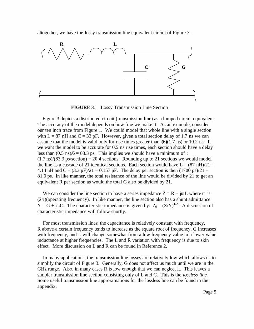
The Ansoft simulation data is shown in Tables 1 and 2.
TABLE 1: Buried Microstrip Simulation: Ideal Rectangular and ActualTrapezoidal
Etch Factor Theta (deg) L (nH/inch) C (pF/inch) Zo (Ohms) %D (IR/AT) Infinite 90.0 8.4833 3.3957 49.982 N/A
1.000 45.0 8.8440 3.2467 52.192 -4.231.732 60.0 8.7302 3.2890 51.521 -2.992.000 63.4 8.7031 3.2992 51.361 -2.683.000 71.6 8.6405 3.3231 50.991 -1.985.000 78.7 8.5873 3.3437 50.677 -1.378.000 82.9 8.5474 3.3593 50.442 -0.91
The infinite etch factor entry (Theta = 90.0) represents the ideal rectangular trace. Thelower the etch factor, the further from the ideal rectangular trace. The lower etch factorsresult in lower capacitance since there is less fringe field from trace to ground. For tpd toremain constant; if C decreases with lower etch factor, then L must increase sincetpd = (LC)1/2. The propagation delay (tpd) is also equal to (tpd-vacuum)(∈r). Since theeffective relative dielectric constant for this configuration does not change with etchfactor, the LC product must be constant. It should be noted that all the simulation valuesare high frequency values. We have not considered dispersion at low frequencies. Forhigh speed digital signaling, this is a reasonable approach.
The %D (IR/AT) entry is the percentage deviation of the characteristic impedance(Z0) of the ideal rectangular cross section (etch factor = infinity) with respect to the actualtrapezoidal cross section.
Figures 10 and 11 are plots of the buried microstrip parameters versus etch factor.
Page 11
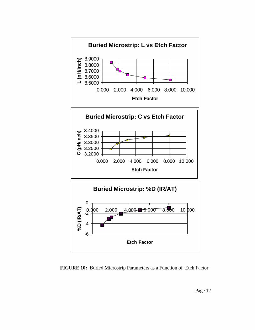
FIGURE 10: Buried Microstrip Parameters as a Function of Etch Factor
Page 12
Buried Microstrip: L vs Etch Factor
8.50008.60008.70008.80008.9000
0.000 2.000 4.000 6.000 8.000 10.000
Etch Factor
L (n
H/in
ch)
Buried Microstrip: C vs Etch Factor
3.20003.25003.30003.35003.4000
0.000 2.000 4.000 6.000 8.000 10.000
Etch Factor
C (p
H/in
ch)
Buried Microstrip: %D (IR/AT)
-6
-4
-2
00.000 2.000 4.000 6.000 8.000 10.000
Etch Factor
%D
(IR
/AT)

FIGURE 11: Buried Microstrip: Z0 versus Etch Factor
The rectangular correction (equivalent rectangle) simulations for buried microstrip istabulated in Table 2.
TABLE 2: Buried Microstrip Simulation: Equivalent RectangularEtch Factor w (mils) L (nH/inch) C (pF/inch) Zo (Ohms) %D (ER/AT)
1.000 3.30 9.1879 3.1252 54.222 3.891.732 3.60 8.8726 3.2362 52.361 1.632.000 3.65 8.8192 3.2677 51.951 1.153.000 3.77 8.7056 3.2983 51.375 0.755.000 3.86 8.6105 3.3347 50.814 0.278.000 3.91 8.5678 3.3513 50.562 0.24
The width (w) of the equivalent rectangular trace is 4.0 mils – H whereH = 0.7/(etch factor).
Comparing to Table 1, we see from Table 2 that: the equivalent rectangular L ishigher for all etch factors than the actual trapezoidal and also that C is lower than theactual trapezoidal for all etch factors. The Z0 of the equivalent rectangular is higherthan Z0 of the actual trapezoidal for all etch factors.
The %D (ER/AT) column is the percentage deviation of the equivalent rectangularZ0 with respect to the actual trapezoidal Z0. Note that the magnitude of these deviationsare somewhat less than the %D (IR/AT) deviations but not by a whole lot (particularlyat lower etch factors). Also note the change in sign.
Page 13
Buried Microstrip: Zo vs Etch Factor
50515253
0.000 2.000 4.000 6.000 8.000 10.000
Etch Factor
Zo (O
hms)

Figures 12 and 13 are plots of the equivalent rectangular buried microstrip parametersas a function of etch factor.
FIGURE 12: Equivalent Rectangular Buried Microstrip Parameters versus Etch Factor
Page 14
Buried Microstrip: Rectangular Equivalent
8.5
9
9.5
0.000 2.000 4.000 6.000 8.000 10.000
Etch Factor
L (n
H/in
ch)
Buried Microstrip: Rectangular Equivalent
3.13.23.33.4
0.000 2.000 4.000 6.000 8.000 10.000
Etch Factor
C (
pF
/inch
)
Buried Microstrip: %D (ER/AT)
0
2
4
6
0.000 2.000 4.000 6.000 8.000 10.000
Etch Factor
%D
(ER
/AT)

FIGURE 13: Equivalent Rectangular Buried Microstrip Z0 versus Etch Factor
Let us now turn our attention to the symmetrical stripline illustrated in Figure 14.
Ground Plane
6.0 6.0 H θ 0.7 0.7
4.0 w
6.0 6.0
Ground Plane
Actual Trapezoidal Equivalent Rectangular (Ideal Rectangular is actual trapezoidal ( w = 4.0 – H ) with θ = 90°)
FIGURE 14: Symmetrical Stripline for Simulation, all dimensions in mils.
Page 15
Buried Microstrip: Zo -- Rectangular Equivalent
50525456
0.000 2.000 4.000 6.000 8.000 10.000
Etch Factor
Zo (O
hms)

In the stripline, return current flows through both ground/power planes. This is a verycommon structure in multilayer printed wiring boards although the spacing in thatapplication tends to be asymmetrical (i.e. the signal conductor will be closer to one planethan the other). As with buried microstrip, we also looked at the equivalent rectangularcross section for the symmetrical stripline. Note that we doubled the spacing from signalto ground plane in an attempt to maintain an impedance similar to the microstrip.Keeping the same spacing would almost double the capacitance and if the capacitancedoubled, the inductance would have to be reduced by half in order to maintain the samepropagation velocity. The combined effect of capacitance and inductance changes wouldbe to cut the characteristic impedance in half.
The tabular simulation data for symmetrical stripline are given in Tables 3 and 4. Themagnitude of the impedance deviations is given in Figure 15.
TABLE 3: Symmetrical Stripline Simulation, Ideal Rectangular and ActualTrapezoidal
Etch Factor Theta (deg) L (nH/inch) C (pF/inch) Zo (Ohms) %D (IR/AT)Infinite 90.0 9.3906 3.0639 55.361 N/A
1.000 45.0 9.8652 2.9220 58.105 -4.721.732 60.0 9.7116 2.9662 57.220 -3.252.000 63.4 9.6743 2.9783 56.994 -2.873.000 71.6 9.5931 3.0049 56.502 -2.025.000 78.7 9.5147 3.0271 56.064 -1.258.000 82.9 9.4720 3.0393 55.826 -0.83
TABLE 4: Symmetrical Stripline Simulation, Equivalent Rectangular
Etch Factor w (mils) L (nH/inch) C (pF/inch) Zo (Ohms) %D (ER/AT)1 3.3 10.113 2.8423 59.649 2.66
1.732 3.6 9.7973 2.9395 57.732 0.892 3.65 9.7438 2.956 57.413 0.743 3.77 9.6173 2.9943 56.673 0.35 3.86 9.5251 3.0219 56.143 0.148 3.91 9.4755 3.0375 55.852 0.05
From Figure 15 we can see that for etch factors greater than 1.7, the equivalentrectangular approach results in less than 1% error for characteristic impedance. Forthese etch factors and if your available field modeling software does not allowtrapezoidal cross sections, a rectangular equivalent model can afford a reasonableaccuracy.
Page 16

FIGURE 15: Characteristic Impedance Deviation With Respect to Actual Trapezoidal Cross Section, Symmetrical Stripline.
High speed digital signaling requirements have led to increased use of differentialsignal transmission. Two popular configurations for differential signal transmission arethe edge-coupled pair and the broadside coupled pair.
Starting with the edge-coupled pair we looked at buried microstrip and surfacemicrostrip. The buried microstrip version is illustrated in Figure 16 and simulationdata is presented in Tables 5 and 6. The magnitude of the impedance deviations isplotted in Figure 17. Note the 6% error between ideal rectangular and actual trapezoidalfor characteristic impedance.
Page 17
% Zo Deviation with respect to actual trapezoidal
0
0.5
1
1.5
2
2.5
3
3.5
4
4.5
5
0.000 1.000 2.000 3.000 4.000 5.000 6.000 7.000 8.000 9.000
Etch Factor
% D
evia
tion
| Ideal Rectangular (Theta = 90 deg.)|
Rectangular Equivalent
Symmetrical Stripline

H θ 0.7
4.0 4.0 4.0
Trapezoidal Cross Section, ( Ideal rectangular ⇒ θ = 90° )
0.7
w s w
w = 4.0 – H s = 4.0 + H
Equivalent Rectangular Cross Section
FIGURE 16: Edge-Coupled Pair, Buried Microstrip
TABLE 5: Edge-Coupled Pair, Buried Microstrip – Ideal Rectangular and ActualTrapezoidal
Etch Factor Theta (deg) L (nH/inch) C (pF/inch) Zo (Ohms) %D (IR/AT) Infinite 90.0 17.444 1.6460 102.95 N/A
1.000 45.0 18.595 1.5442 109.74 -6.191.732 60.0 18.230 1.5751 107.58 -4.302.000 63.4 18.173 1.5800 107.25 -4.013.000 71.6 17.958 1.5989 105.98 -2.865.000 78.7 17.757 1.6170 104.79 -1.768.000 82.9 17.642 1.6275 104.12 -1.12
TABLE 6: Edge-Coupled Pair, Buried Microstrip – Equivalent RectangularEtch Factor w (mils) s (mils) L (nH/inch) C (pF/inch) Zo (Ohms) % D (ER/AT)
1.000 3.30 4.70 19.275 1.4897 113.75 3.651.732 3.60 4.40 18.463 1.5552 108.96 1.282.000 3.65 4.35 18.333 1.5663 108.19 1.553.000 3.77 4.23 18.047 1.5938 106.41 0.415.000 3.86 4.14 17.784 1.6146 104.95 0.158.000 3.91 4.09 17.659 1.6260 104.22 0.01
Page 18
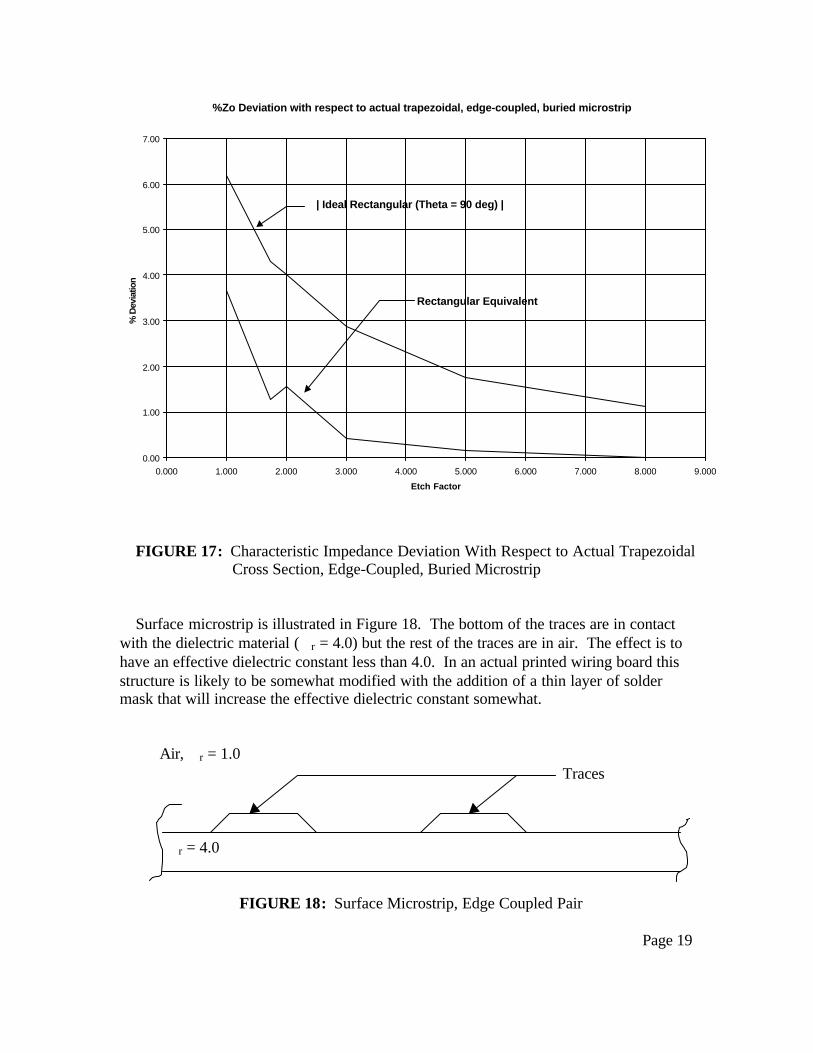
FIGURE 17: Characteristic Impedance Deviation With Respect to Actual Trapezoidal Cross Section, Edge-Coupled, Buried Microstrip
Surface microstrip is illustrated in Figure 18. The bottom of the traces are in contactwith the dielectric material (∈r = 4.0) but the rest of the traces are in air. The effect is tohave an effective dielectric constant less than 4.0. In an actual printed wiring board thisstructure is likely to be somewhat modified with the addition of a thin layer of soldermask that will increase the effective dielectric constant somewhat.
Air, ∈r = 1.0 Traces
∈r = 4.0
FIGURE 18: Surface Microstrip, Edge Coupled Pair
Page 19
%Zo Deviation with respect to actual trapezoidal, edge-coupled, buried microstrip
0.00
1.00
2.00
3.00
4.00
5.00
6.00
7.00
0.000 1.000 2.000 3.000 4.000 5.000 6.000 7.000 8.000 9.000
Etch Factor
% D
evia
tion
| Ideal Rectangular (Theta = 90 deg) |
Rectangular Equivalent
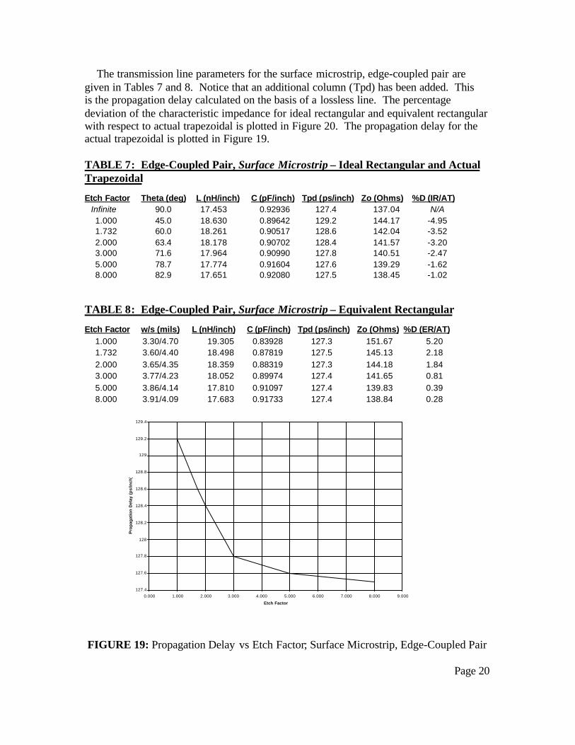
The transmission line parameters for the surface microstrip, edge-coupled pair aregiven in Tables 7 and 8. Notice that an additional column (Tpd) has been added. Thisis the propagation delay calculated on the basis of a lossless line. The percentagedeviation of the characteristic impedance for ideal rectangular and equivalent rectangularwith respect to actual trapezoidal is plotted in Figure 20. The propagation delay for theactual trapezoidal is plotted in Figure 19.
TABLE 7: Edge-Coupled Pair, Surface Microstrip – Ideal Rectangular and ActualTrapezoidal
Etch Factor Theta (deg) L (nH/inch) C (pF/inch) Tpd (ps/inch) Zo (Ohms) %D (IR/AT) Infinite 90.0 17.453 0.92936 127.4 137.04 N/A
1.000 45.0 18.630 0.89642 129.2 144.17 -4.951.732 60.0 18.261 0.90517 128.6 142.04 -3.522.000 63.4 18.178 0.90702 128.4 141.57 -3.203.000 71.6 17.964 0.90990 127.8 140.51 -2.475.000 78.7 17.774 0.91604 127.6 139.29 -1.628.000 82.9 17.651 0.92080 127.5 138.45 -1.02
TABLE 8: Edge-Coupled Pair, Surface Microstrip – Equivalent Rectangular
Etch Factor w/s (mils) L (nH/inch) C (pF/inch) Tpd (ps/inch) Zo (Ohms) %D (ER/AT)1.000 3.30/4.70 19.305 0.83928 127.3 151.67 5.201.732 3.60/4.40 18.498 0.87819 127.5 145.13 2.182.000 3.65/4.35 18.359 0.88319 127.3 144.18 1.843.000 3.77/4.23 18.052 0.89974 127.4 141.65 0.815.000 3.86/4.14 17.810 0.91097 127.4 139.83 0.398.000 3.91/4.09 17.683 0.91733 127.4 138.84 0.28
FIGURE 19: Propagation Delay vs Etch Factor; Surface Microstrip, Edge-Coupled Pair
Page 20
127.4
127.6
127.8
128
128.2
128.4
128.6
128.8
129
129.2
129.4
0.000 1.000 2.000 3.000 4.000 5.000 6.000 7.000 8.000 9.000
Etch Factor
Pro
paga
tion
Del
ay (
ps/in
ch)

FIGURE 20: Characteristic Impedance Deviation With Respect to Actual Trapezoidal Cross Section; Edge-Coupled, Surface Microstrip
The broadside-coupled pair is another conductor configuration that finds application indifferential signaling. This configuration is illustrated in Figure 21. The inverted versionis not recommended as this implies that the conductors are on separate cores and thussubject to misalignment. Table 9 provides simulation data for the actual trapezoidaltraces. Table 10 provides simulation data for the equivalent rectangular with the“%D (ER/AT)” column pertaining to the Table 9 trapezoidal values. The invertedtrapezoidal data is presented in Table 11. Impedance deviation for the normal (notinverted) trapezoidal cross section is given in Figure 22.
Page 21
0.00
1.00
2.00
3.00
4.00
5.00
6.00
0.000 1.000 2.000 3.000 4.000 5.000 6.000 7.000 8.000 9.000
Etch Factor
% D
evia
tion
|Ideal Rectangular (Theta = 90 degrees) |
Rectangular Equivalent

x w 0.7 mil 4.0 mil
4.0 mil 3.0 mil x
θ 0.7 mil (not recommended)
NORMAL Equivalent Inverted Trapezoidal TRAPEZOIDAL Rectangular
FIGURE 21: Broadside-Coupled Pair
TABLE 9: Broadside-Coupled Pair – Normal Configuration – Ideal Rectangularand Actual Trapezoidal
Etch Factor Theta (deg) L (nH/inch) C (pF/inch) Zo (Ohms) %D (IR/AT) Infinite 90.0 11.499 2.4971 67.859 N/A
1.000 45.0 12.306 2.3856 71.822 -5.511.732 60.0 11.877 2.4176 70.090 -3.182.000 63.4 11.822 2.4288 69.768 -2.743.000 71.6 11.732 2.4475 69.235 -1.995.000 78.7 11.646 2.4654 68.730 -1.278.000 82.9 11.590 2.4775 68.395 -0.78
TABLE 10: Broadside-Coupled Pair – Equivalent Rectangular – (%D referenced toNomal Trapezoidal)
Etch Factor w (mils) L (nH/inch) C (nH/inch) Zo (Ohms) %D (ER/AT)1.000 3.30 12.724 2.2566 75.091 4.551.732 3.60 12.168 2.3597 71.810 2.452.000 3.65 12.078 2.3774 71.275 2.163.000 3.77 11.871 2.4187 70.058 1.185.000 3.86 11.726 2.4488 69.199 0.688.000 3.91 11.641 2.4665 68.701 0.45
Page 22
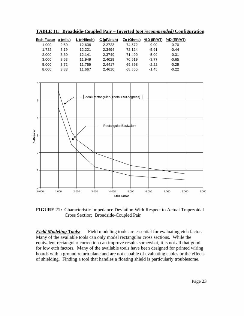
TABLE 11: Broadside-Coupled Pair – Inverted (not recommended) Configuration
Etch Factor x (mils) L (nH/inch) C (pF/inch) Zo (Ohms) %D (IR/AT) %D (ER/AT)1.000 2.60 12.636 2.2723 74.572 -9.00 0.701.732 3.19 12.221 2.3494 72.124 -5.91 -0.442.000 3.30 12.141 2.3749 71.499 -5.09 -0.313.000 3.53 11.949 2.4029 70.519 -3.77 -0.655.000 3.72 11.759 2.4417 69.398 -2.22 -0.298.000 3.83 11.667 2.4610 68.855 -1.45 -0.22
FIGURE 21: Characteristic Impedance Deviation With Respect to Actual Trapezoidal Cross Section; Broadside-Coupled Pair
Field Modeling Tools: Field modeling tools are essential for evaluating etch factor.Many of the available tools can only model rectangular cross sections. While theequivalent rectangular correction can improve results somewhat, it is not all that goodfor low etch factors. Many of the available tools have been designed for printed wiringboards with a ground return plane and are not capable of evaluating cables or the effectsof shielding. Finding a tool that handles a floating shield is particularly troublesome.
Page 23
0
1
2
3
4
5
6
0.000 1.000 2.000 3.000 4.000 5.000 6.000 7.000 8.000 9.000
Etch Factor
% D
evia
tion
| Ideal Rectangular (Theta = 90 degrees) |
Rectangular Equivalent

We used Ansoft software to model the etch factor. This tool set can handle cables,non rectangular cross sections, and shielding effects. The Ansoft package is a suite oftools that includes the Maxwell 2D field solver that was used for our evaluation. The2D tool requires that the transmission line section being analyzed have a uniform butnot necessarily rectangular cross section. For non uniform structures Ansoft offers a3D tool as well.
The Maxwell 2D solver uses geometry and material properties such as dielectricconstant, resistivity, line width, line thickness, etceteras as inputs. Using finiteelement analysis Maxwell 2D provides electrical parameter outputs such as Z0, Cij, Lij,etc. In addition, it can provide frequency sweeps such as L versus frequency and Rversus frequency. Many of the board modeling tools provide only the high frequencysolution.
The Ansoft tool has allowed us to establish design guidelines. It can provide absoluteaccuracy better than one percent. It allowed us to do a lot of quick “what if” evaluations.In general, this tool has allowed us to avoid expensive and time consuming cut and tryhardware iterations.
As useful as the Ansoft tool is, it does have some drawbacks. The tool is not userfriendly. It almost always provides an answer. The answer may not always be right.The user must be familiar enough with transmission line theory to detect grossinaccuracies. If these inaccuracies are found to exist parameters such as accuracy andmeshing must be adjusted. It is useful to perform a frequency sweep of resistance. IfR versus f levels off in the frequency range of interest, a finer mesh should be applied.The power and versatility of the tool has resulted in a rather complex arrangement thatprecludes casual use. There is a steep learning curve.
Conclusions: Higher edge rates and clocks in digital logic force us to use transmission line analysisand impedance control.
Low etch factor increases impedance in excess of six percent for some configurations.
Etch factor varies from vendor to vendor due to different processes and equipment.
Etch factor can vary with the same vendor due to production at different plants or therefurbishing of old plants.
The rectangular correction factor is not all that good for low etch factors.
Appropriate field modeling tools are needed to fully evaluate etch factor.
Page 24

References:
1] Johnson, Howard W. and Martin Graham, High-Speed Digital Design: A Handbook of Black Magic, PTR Prentice-Hall, 1993, ISBN 0-13-395724-1.
2] Buhler, tto and Charles Grasso, “Transmission Line Inductance and Proximity Effect,” 10th Annual IEEE EMC Society (Rocky Mountain Chapter) Regional Symposium, Tuesday, May 23, 2000 at the Holiday Inn, Denver Northglenn, 10 East 120th Avenue, Northglenn, Colorado.
3] Bogatin, Eric, “Impedance Calculations,” November 1, 1999. Available as ID #73 from http://www.GigaTest.com
4] Printed Circuits Handbook, Coombs, Clyde F. Jr. ed., third edition, McGraw-Hill, 1988, ISBN 0-07-012609-7, pp 14.28 – 14.33.
6] Handbook of Flexible Circuits, Gilleo, Ken ed., Van Nostrand Reinhold, 1992, ISBN 0-442-00168-1, pp 45, 244.
Appendix (see next page)
Page 25

TRANSMISSION LINE CRIB SHEET _
Equivalent electrical circuit, Lossless Lumped Constant
L L
C C
L & C should be chosen such that Tpd per section < (Tr)/6, where Tr = rise time of signal- - - - - - - - - - - - - - - - - - - - - - - - - - - - - - - - - - - - - - - - - - - - - - - - - - - - - - - - - - - - - -
Z0 = L/C Z0 = Characteristic impedance of transmission line in ΩΩ .
L = Transmission line inductance per unit length.
C = Transmission line capacitance per unit length.
Tpd = LC Tpd = Transmission line signal delay per unit length.
vp = c ∈∈r vp = Transmission line velocity of propagation.
c = velocity of light in vacuum (299,792,458 m/s ≈≈ 11.803 in/ns ≈≈ 0.9836 ft/ns)
∈∈ r = relative dielectric constant of transmission line.
Tpd = (Tpd-vacuum) ∈∈ r Tpd-vacuum = 84.723 ps/inch
∈∈r = ( Tpd/Tpd-vacuum)2
λλf = c in vacuum λλ = wavelength
λλf = vp in dielectric f = frequency
C = Tpd/Z0
L = Z0Tpd
Page 26

TRANSMISSION LINE CRIB SHEET (continued): TDR Relationships _
ρρ = ZL – Z0 _ ρρ = reflection coefficient (-1.0 to +1.0). ZL + Z0
ZL = Load impedance in ΩΩ .ZL = Z0(1 + ρρ ) _ (1 + ρρ )
A useful approximation for moderate mismatch ρρ ≈≈ (mismatch)/2 mismatch 20 % high mismatch 5 % high ρρ = 9.09 % ρρ ≈≈ 10 % ρρ = 2.43 % ρρ ≈≈ 2.5 %
mismatch 20 % low mismatch 5 % low ρρ = -11.11 % ρρ ≈≈ -10 % ρρ = -2.56 % ρρ ≈≈ - 2.5 %
Page 27