Embed Size (px)
Citation preview
The Basics of Serial Data Compliance andValidation Measurements
Pr
im
er
1
Table of Contents
2 www.tektronix.com/serial_data
Introduction: A Definition of Serial Compliance and Validation . . . . . . . . . . . . . . . . . . . . . . . . . . . .3
A Transition In Progress: From Parallel To Serial Data Architectures . . . . . . . . . . . . . . . . . . . . . . .3
Building A Framework of Standards . . . . . . . . . . . . . . . . . . . . . . . . . . . . . . . . . . . . . . . . . . . . . . . . . . . . . . . . . . . . . . . . . . . . . . . . . . . .3
Understanding Serial Architectures — The Common Threads . . . . . . . . . . . . . . . . . . . . . . . . . . . . .4
High Signaling Frequencies and Data Rates . . . . . . . . . . . . . . . . . . . . . . . . . . . . . . . . . . . . . . . . . . . . . . . . . . . . . . . . . . . . . . . . . . . . . .4
Differential Signaling . . . . . . . . . . . . . . . . . . . . . . . . . . . . . . . . . . . . . . . . . . . . . . . . . . . . . . . . . . . . . . . . . . . . . . . . . . . . . . . . . . . . . .4
A "Stack" Architecture . . . . . . . . . . . . . . . . . . . . . . . . . . . . . . . . . . . . . . . . . . . . . . . . . . . . . . . . . . . . . . . . . . . . . . . . . . . . . . . . . . . . .5
Packetized Data . . . . . . . . . . . . . . . . . . . . . . . . . . . . . . . . . . . . . . . . . . . . . . . . . . . . . . . . . . . . . . . . . . . . . . . . . . . . . . . . . . . . . . . . .6
Characteristics of the Physical Layer . . . . . . . . . . . . . . . . . . . . . . . . . . . . . . . . . . . . . . . . . . . . . . . . . . . . . . . . . . . . . . . . . . . . . . . . . . .6
Physical Layer Compliance Testing: An Analog View Of A Digital World . . . . . . . . . . . . . . . . . . . . .7
Differing Standards, Common Compliance Measurements . . . . . . . . . . . . . . . . . . . . . . . . . . . . . . . . . . . . . . . . . . . . . . . . . . . . . . . . . . . .8
Amplitude Measurements . . . . . . . . . . . . . . . . . . . . . . . . . . . . . . . . . . . . . . . . . . . . . . . . . . . . . . . . . . . . . . . . . . . . . . . . . . . . . . . . . . .8
Timing Measurements . . . . . . . . . . . . . . . . . . . . . . . . . . . . . . . . . . . . . . . . . . . . . . . . . . . . . . . . . . . . . . . . . . . . . . . . . . . . . . . . . . . . .8
Jitter Measurements . . . . . . . . . . . . . . . . . . . . . . . . . . . . . . . . . . . . . . . . . . . . . . . . . . . . . . . . . . . . . . . . . . . . . . . . . . . . . . . . . . . . . .9
Mask Testing of Eye Diagrams . . . . . . . . . . . . . . . . . . . . . . . . . . . . . . . . . . . . . . . . . . . . . . . . . . . . . . . . . . . . . . . . . . . . . . . . . . . . . . .9
Measurements on Optical Signals . . . . . . . . . . . . . . . . . . . . . . . . . . . . . . . . . . . . . . . . . . . . . . . . . . . . . . . . . . . . . . . . . . . . . . . . . . . .11
Overview of Serial Measurement Solutions . . . . . . . . . . . . . . . . . . . . . . . . . . . . . . . . . . . . . . . . . . .12
Real-time Oscilloscopes . . . . . . . . . . . . . . . . . . . . . . . . . . . . . . . . . . . . . . . . . . . . . . . . . . . . . . . . . . . . . . . . . . . . . . . . . . . . . . . . . . .13
Sampling Oscilloscopes . . . . . . . . . . . . . . . . . . . . . . . . . . . . . . . . . . . . . . . . . . . . . . . . . . . . . . . . . . . . . . . . . . . . . . . . . . . . . . . . . . .13
Logic Analyzers . . . . . . . . . . . . . . . . . . . . . . . . . . . . . . . . . . . . . . . . . . . . . . . . . . . . . . . . . . . . . . . . . . . . . . . . . . . . . . . . . . . . . . . . .13
Signal Sources . . . . . . . . . . . . . . . . . . . . . . . . . . . . . . . . . . . . . . . . . . . . . . . . . . . . . . . . . . . . . . . . . . . . . . . . . . . . . . . . . . . . . . . . .13
Analog Compliance Measurement Considerations: Probing . . . . . . . . . . . . . . . . . . . . . . . . . . . . . .14
Connecting to the Serial Device Under Test . . . . . . . . . . . . . . . . . . . . . . . . . . . . . . . . . . . . . . . . . . . . . . . . . . . . . . . . . . . . . . . . . . . . .14
Compliance Measurement Considerations: Acquisition . . . . . . . . . . . . . . . . . . . . . . . . . . . . . . . . .16
Acquisition System Performance Drives Measurement Accuracy . . . . . . . . . . . . . . . . . . . . . . . . . . . . . . . . . . . . . . . . . . . . . . . . . . . . . .16
Evaluating the Acquisition System’s Analog Performance . . . . . . . . . . . . . . . . . . . . . . . . . . . . . . . . . . . . . . . . . . . . . . . . . . . . . . . . . . . .17
Evaluating Digital Performance . . . . . . . . . . . . . . . . . . . . . . . . . . . . . . . . . . . . . . . . . . . . . . . . . . . . . . . . . . . . . . . . . . . . . . . . . . . . . .17
Compliance Measurement Considerations: Analysis . . . . . . . . . . . . . . . . . . . . . . . . . . . . . . . . . . . .18
Getting a Handle on all that Data . . . . . . . . . . . . . . . . . . . . . . . . . . . . . . . . . . . . . . . . . . . . . . . . . . . . . . . . . . . . . . . . . . . . . . . . . . . .19
Thinking Beyond Compliance Testing . . . . . . . . . . . . . . . . . . . . . . . . . . . . . . . . . . . . . . . . . . . . . . . .19
A Digital Tool for Digital Tasks . . . . . . . . . . . . . . . . . . . . . . . . . . . . . . . . . . . . . . . . . . . . . . . . . . . . . . . . . . . . . . . . . . . . . . . . . . . . . .19
Probing Means Making the Right Connections . . . . . . . . . . . . . . . . . . . . . . . . . . . . . . . . . . . . . . . . . . . . . . . . . . . . . . . . . . . . . . . . . . .20
Acquiring the Signal: from Packet to Parallel . . . . . . . . . . . . . . . . . . . . . . . . . . . . . . . . . . . . . . . . . . . . . . . . . . . . . . . . . . . . . . . . . . . .20
Triggering is the Key to Efficiency in Troubleshooting . . . . . . . . . . . . . . . . . . . . . . . . . . . . . . . . . . . . . . . . . . . . . . . . . . . . . . . . . . . . . .22
New Synchronization Modes Stay in Step with Serial Requirements . . . . . . . . . . . . . . . . . . . . . . . . . . . . . . . . . . . . . . . . . . . . . . . . . . . .22
Analyzing the Results . . . . . . . . . . . . . . . . . . . . . . . . . . . . . . . . . . . . . . . . . . . . . . . . . . . . . . . . . . . . . . . . . . . . . . . . . . . . . . . . . . . .23
Summary . . . . . . . . . . . . . . . . . . . . . . . . . . . . . . . . . . . . . . . . . . . . . . . . . . . . . . . . . . . . . . . . . . . . . .24
22
The Basics Of Serial Data Compliance and Validation MeasurementsPrimer
Introduction: A Definition of SerialCompliance and Validation
In the computing and communications industries, a degree of stan-
dardization at the system, subsystem, and component levels is the
foundation that technology builds upon. Examples of standardization
range from LVDS signaling to the PCI Express serial bus designed to
replace current PCI technology. Standards pervade semiconductor
architectures, network protocols, and software components. And for
every standard, there must be some means of certification, some
way to prove that new products are in compliance with the standard.
Serial data architectures, and the standards that support them, are
the next frontier in digital design. Industry committees announce
new serial standards or refinements at almost every major industry
event. Inevitably, the emerging standards call for certification
procedures involving electronic test and measurement equipment:
oscilloscopes, logic analyzers, signal sources, and more. There is
an urgent need for expert, efficient solutions that can speed the
process—still unfamiliar to many designers—of serial compliance
and validation measurement.
This primer deals with the challenges of serial device compliance
testing, validation, and troubleshooting. The discussion in the
ensuing pages covers basic principles, measurement requirements,
and tools for troubleshooting, all in the context of the latest serial
transmission technologies. The primer is designed to help you
understand the common aspects of serial data transmission; to
explain the analog and digital measurement requirements that apply
to these emerging serial techniques, and to provide an overview of
the test and measurement solutions that support both compliance
tests and troubleshooting work.
A Transition In Progress: FromParallel To Serial Data Architectures
Parallel data transmission architectures dominate digital systems,
but there is change in the wind. Parallel constructs are nearing their
practical bandwidth limits, and there is a tremendous need for an
order-of-magnitude increase in data throughput.
In recent years there has been a major industry push toward serial
data transmission technologies to address this need. But the change
will not occur overnight. Currently we are in the midst of a transition,
and both architectures are alive and well. There is at least one more
generation of parallel technology to come, a fact implied by some of
the latest specifications. The PCI-SIG, for example, has defined both
PCI-X 2.0 (parallel) and PCI Express (serial) formats. But serial data
architecture is virtually certain to prevail as data rates continue to
escalate. It provides some key benefits over parallel data transfer:
Higher bandwidth per pin
Scalable performance through the use of aggregated lanes
Lower overhead and latency (maximizes payload efficiency)
It all adds up to a wide range of measurement needs. Design and vali-
dation engineers, accustomed to working on parallel buses, will need to
perform system-level testing and debug on serial technologies as well.
Building A Framework of Standards
The key to the success of any emerging standard is a systematic
plan to address specifications, testing, and compliance require-
ments. Typically such plans are developed by industry working
groups. Companies with an interest in supporting a new proposal
work cooperatively to develop and stabilize standards and define
qualification criteria. Interoperability does not occur in a vacuum,
and the only way for a company to keep pace with emerging stan-
dards is to participate in the committees and working groups that
develop them. Standards typically include measurement require-
ments and in many cases, specific test equipment recommendations
as well. Tests are usually performed at “plug fests” where prospec-
tive vendors gather to evaluate their products for interoperability
and compliance with the standard.
3www.tektronix.com/serial_data
The Basics Of Serial Data Compliance and Validation MeasurementsPrimer
InfiniBand and PCI Express are two 2.5 Gb/s standards. InfiniBand
has found its niche in high-performance computing, while PCI
Express is growing fast in its inclusion in product roadmaps. Other
examples of serial data specifications with data rates ranging from
1 Gb/s to 3.2 Gb/s include:
Serial ATA
IEEE 1394B (Firewire)
FibreChannel
1 GbE Serial (1000Base-CX)
10 GbE XAUI
10 GFC XAUI
RapidIO
And others still emerging
Understanding Serial Architectures—The Common Threads
As summarized earlier, there are numerous serial technologies
evolving now, and more to come. While each of these protocols has
its own unique qualities, most of them share some fundamental
characteristics, particularly in the areas of bandwidth, signaling,
protocol architecture and data formatting.
High Signaling Frequencies and Data Rates
Serial data signaling is achieved by embedding the clock and data
in the same transmission media. The SerDes (Serial Deserializer)
found in all links is responsible for Serializing the data when trans-
mitted, and deserializing it when received. By embedding the clock
in the data bit stream, less pins are used to achieve the same data
transfer rate and many traditional testing concerns, such as setup
and hold time and clock-data jitter are avoided. However, the clock
and data still need to be recovered by a receiver in a serial data
serdes. Thus excessive jitter can cause the receiver not to recover
the clock correctly and cause bit errors.
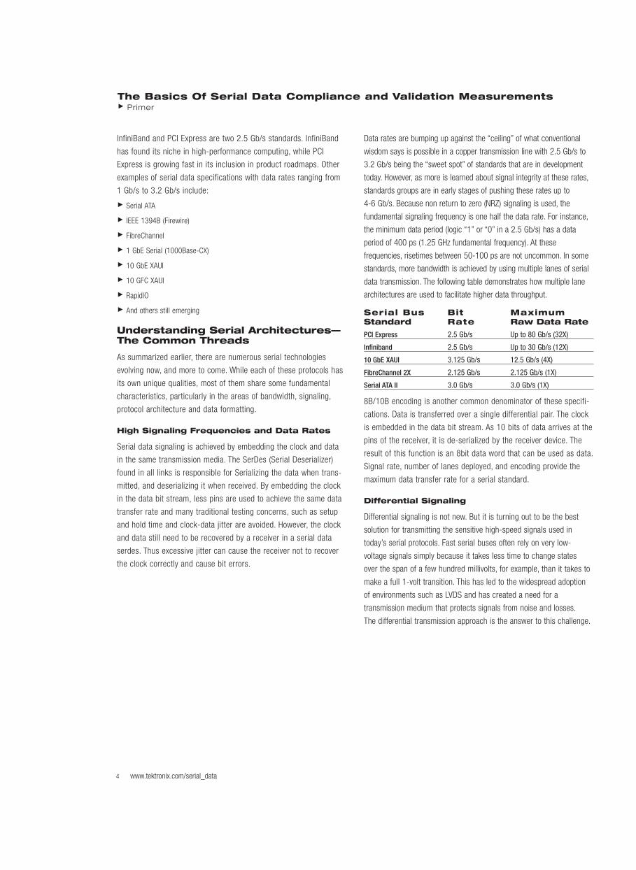
Data rates are bumping up against the “ceiling” of what conventional
wisdom says is possible in a copper transmission line with 2.5 Gb/s to
3.2 Gb/s being the “sweet spot” of standards that are in development
today. However, as more is learned about signal integrity at these rates,
standards groups are in early stages of pushing these rates up to
4-6 Gb/s. Because non return to zero (NRZ) signaling is used, the
fundamental signaling frequency is one half the data rate. For instance,
the minimum data period (logic “1” or “0” in a 2.5 Gb/s) has a data
period of 400 ps (1.25 GHz fundamental frequency). At these
frequencies, risetimes between 50-100 ps are not uncommon. In some
standards, more bandwidth is achieved by using multiple lanes of serial
data transmission. The following table demonstrates how multiple lane
architectures are used to facilitate higher data throughput.
Serial Bus Bit MaximumStandard Rate Raw Data Rate
PCI Express 2.5 Gb/s Up to 80 Gb/s (32X)
Infiniband 2.5 Gb/s Up to 30 Gb/s (12X)
10 GbE XAUI 3.125 Gb/s 12.5 Gb/s (4X)
FibreChannel 2X 2.125 Gb/s 2.125 Gb/s (1X)
Serial ATA II 3.0 Gb/s 3.0 Gb/s (1X)
8B/10B encoding is another common denominator of these specifi-
cations. Data is transferred over a single differential pair. The clock
is embedded in the data bit stream. As 10 bits of data arrives at the
pins of the receiver, it is de-serialized by the receiver device. The
result of this function is an 8bit data word that can be used as data.
Signal rate, number of lanes deployed, and encoding provide the
maximum data transfer rate for a serial standard.
Differential Signaling
Differential signaling is not new. But it is turning out to be the best
solution for transmitting the sensitive high-speed signals used in
today’s serial protocols. Fast serial buses often rely on very low-
voltage signals simply because it takes less time to change states
over the span of a few hundred millivolts, for example, than it takes to
make a full 1-volt transition. This has led to the widespread adoption
of environments such as LVDS and has created a need for a
transmission medium that protects signals from noise and losses.
The differential transmission approach is the answer to this challenge.
4 www.tektronix.com/serial_data
The Basics Of Serial Data Compliance and Validation MeasurementsPrimer
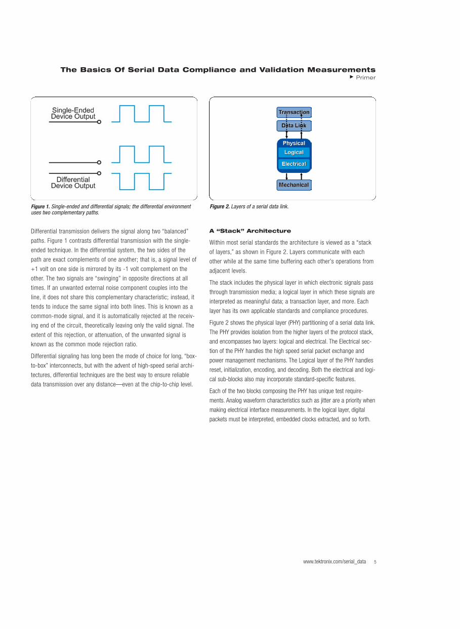
Differential transmission delivers the signal along two “balanced”
paths. Figure 1 contrasts differential transmission with the single-
ended technique. In the differential system, the two sides of the
path are exact complements of one another; that is, a signal level of
+1 volt on one side is mirrored by its -1 volt complement on the
other. The two signals are “swinging” in opposite directions at all
times. If an unwanted external noise component couples into the
line, it does not share this complementary characteristic; instead, it
tends to induce the same signal into both lines. This is known as a
common-mode signal, and it is automatically rejected at the receiv-
ing end of the circuit, theoretically leaving only the valid signal. The
extent of this rejection, or attenuation, of the unwanted signal is
known as the common mode rejection ratio.
Differential signaling has long been the mode of choice for long, “box-
to-box” interconnects, but with the advent of high-speed serial archi-
tectures, differential techniques are the best way to ensure reliable
data transmission over any distance—even at the chip-to-chip level.
A “Stack” Architecture
Within most serial standards the architecture is viewed as a “stack
of layers,” as shown in Figure 2. Layers communicate with each
other while at the same time buffering each other’s operations from
adjacent levels.
The stack includes the physical layer in which electronic signals pass
through transmission media; a logical layer in which these signals are
interpreted as meaningful data; a transaction layer, and more. Each
layer has its own applicable standards and compliance procedures.
Figure 2 shows the physical layer (PHY) partitioning of a serial data link.
The PHY provides isolation from the higher layers of the protocol stack,
and encompasses two layers: logical and electrical. The Electrical sec-
tion of the PHY handles the high speed serial packet exchange and
power management mechanisms. The Logical layer of the PHY handles
reset, initialization, encoding, and decoding. Both the electrical and logi-
cal sub-blocks also may incorporate standard-specific features.
Each of the two blocks composing the PHY has unique test require-
ments. Analog waveform characteristics such as jitter are a priority when
making electrical interface measurements. In the logical layer, digital
packets must be interpreted, embedded clocks extracted, and so forth.
5www.tektronix.com/serial_data
Figure 2. Layers of a serial data link.Figure 1. Single-ended and differential signals; the differential environmentuses two complementary paths.
The Basics Of Serial Data Compliance and Validation MeasurementsPrimer
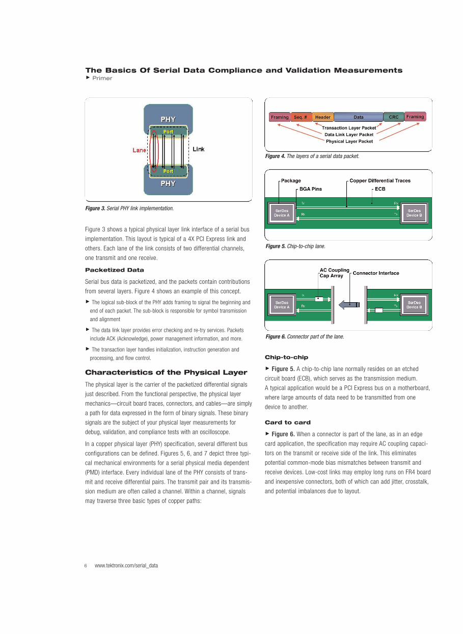
Figure 3 shows a typical physical layer link interface of a serial bus
implementation. This layout is typical of a 4X PCI Express link and
others. Each lane of the link consists of two differential channels,
one transmit and one receive.
Packetized Data
Serial bus data is packetized, and the packets contain contributions
from several layers. Figure 4 shows an example of this concept.
The logical sub-block of the PHY adds framing to signal the beginning and
end of each packet. The sub-block is responsible for symbol transmission
and alignment
The data link layer provides error checking and re-try services. Packets
include ACK (Acknowledge), power management information, and more.
The transaction layer handles initialization, instruction generation and
processing, and flow control.
Characteristics of the Physical Layer
The physical layer is the carrier of the packetized differential signals
just described. From the functional perspective, the physical layer
mechanics—circuit board traces, connectors, and cables—are simply
a path for data expressed in the form of binary signals. These binary
signals are the subject of your physical layer measurements for
debug, validation, and compliance tests with an oscilloscope.
In a copper physical layer (PHY) specification, several different bus
configurations can be defined. Figures 5, 6, and 7 depict three typi-
cal mechanical environments for a serial physical media dependent
(PMD) interface. Every individual lane of the PHY consists of trans-
mit and receive differential pairs. The transmit pair and its transmis-
sion medium are often called a channel. Within a channel, signals
may traverse three basic types of copper paths:
Chip-to-chip
Figure 5. A chip-to-chip lane normally resides on an etched
circuit board (ECB), which serves as the transmission medium.
A typical application would be a PCI Express bus on a motherboard,
where large amounts of data need to be transmitted from one
device to another.
Card to card
Figure 6. When a connector is part of the lane, as in an edge
card application, the specification may require AC coupling capaci-
tors on the transmit or receive side of the link. This eliminates
potential common-mode bias mismatches between transmit and
receive devices. Low-cost links may employ long runs on FR4 board
and inexpensive connectors, both of which can add jitter, crosstalk,
and potential imbalances due to layout.
6 www.tektronix.com/serial_data
Figure 5. Chip-to-chip lane.
Figure 6. Connector part of the lane.
Figure 3. Serial PHY link implementation.
Figure 4. The layers of a serial data packet.
The Basics Of Serial Data Compliance and Validation MeasurementsPrimer
Card to Cable
Figure 7. Introducing a cable connection into the lane adds yet
another source of loss and jitter. Cable-connected serial links are
prevalent in server applications such as InfiniBand; in storage appli-
cations such as Serial ATA and FibreChannel; and in peripheral
applications such as 1394B.
A cabled system as in Figure 7 includes contributions from the max-
imum potential number of vendors. Compliance and interoperability
testing are key to the success of any product in which many inde-
pendently-developed elements must function together flawlessly.
This is especially true in the early stages of a standard’s lifecycle,
when details are still in flux and interpretations may vary.
All standards address the important issue of transmit and receive loss
budgets. They also define compliance test points at which system-level
testing must be performed. Essentially, compliance points are those at
which system components (usually from different vendors) need to inter-
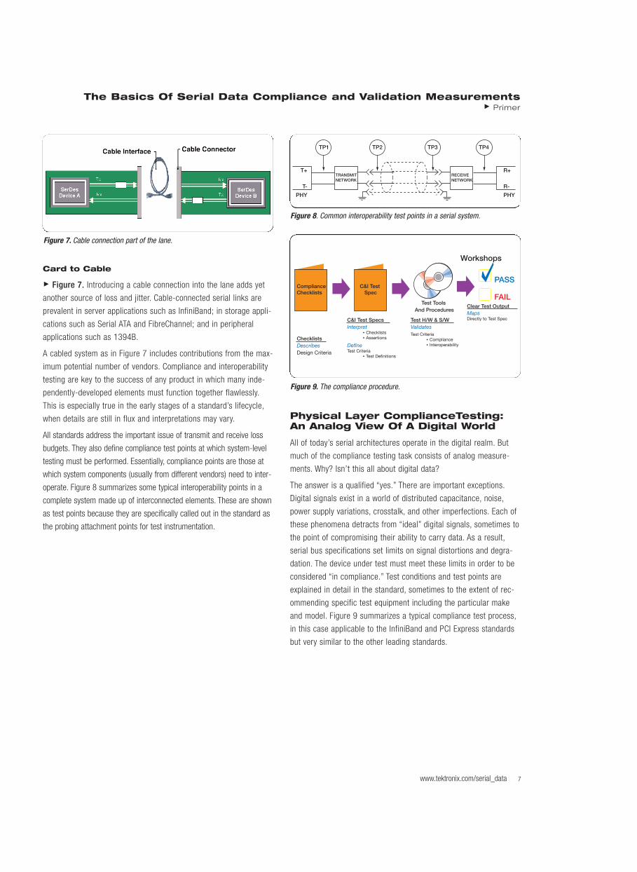
operate. Figure 8 summarizes some typical interoperability points in a
complete system made up of interconnected elements. These are shown
as test points because they are specifically called out in the standard as
the probing attachment points for test instrumentation.
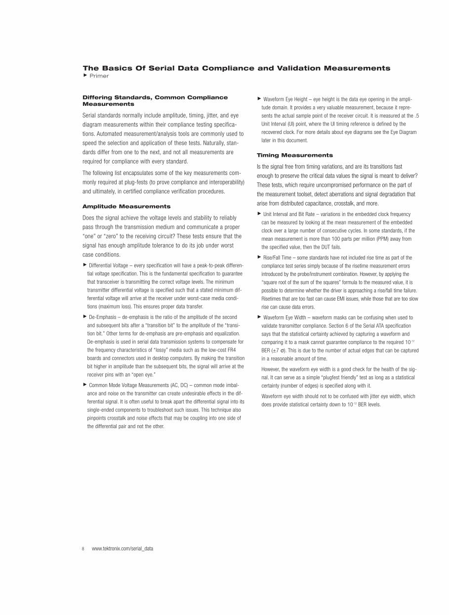
Physical Layer ComplianceTesting:An Analog View Of A Digital World
All of today’s serial architectures operate in the digital realm. But
much of the compliance testing task consists of analog measure-
ments. Why? Isn’t this all about digital data?
The answer is a qualified “yes.” There are important exceptions.
Digital signals exist in a world of distributed capacitance, noise,
power supply variations, crosstalk, and other imperfections. Each of
these phenomena detracts from “ideal” digital signals, sometimes to
the point of compromising their ability to carry data. As a result,
serial bus specifications set limits on signal distortions and degra-
dation. The device under test must meet these limits in order to be
considered “in compliance.” Test conditions and test points are
explained in detail in the standard, sometimes to the extent of rec-
ommending specific test equipment including the particular make
and model. Figure 9 summarizes a typical compliance test process,
in this case applicable to the InfiniBand and PCI Express standards
but very similar to the other leading standards.
7www.tektronix.com/serial_data
ChecklistsDescribesDesign Criteria
Compliance Checklists
C&I Test Spec
C&I Test SpecsInterpret • Checklists • Assertions
Test H/W & S/WValidatesTest Criteria • Compliance • Interoperability
Test Tools And Procedures
Clear Test OutputMapsDirectly to Test Spec
PASS
FAIL
Workshops
DefineTest Criteria • Test Definitions
Figure 9. The compliance procedure.
PHY
T+
TP1 TP2 TP3 TP4
T-
PHY
R+
R-
TRANSMITNETWORK
RECEIVENETWORK
Figure 8. Common interoperability test points in a serial system.
Figure 7. Cable connection part of the lane.
The Basics Of Serial Data Compliance and Validation MeasurementsPrimer
Differing Standards, Common ComplianceMeasurements
Serial standards normally include amplitude, timing, jitter, and eye
diagram measurements within their compliance testing specifica-
tions. Automated measurement/analysis tools are commonly used to
speed the selection and application of these tests. Naturally, stan-
dards differ from one to the next, and not all measurements are
required for compliance with every standard.
The following list encapsulates some of the key measurements com-
monly required at plug-fests (to prove compliance and interoperability)
and ultimately, in certified compliance verification procedures.
Amplitude Measurements
Does the signal achieve the voltage levels and stability to reliably
pass through the transmission medium and communicate a proper
“one” or “zero” to the receiving circuit? These tests ensure that the
signal has enough amplitude tolerance to do its job under worst
case conditions.
Differential Voltage – every specification will have a peak-to-peak differen-
tial voltage specification. This is the fundamental specification to guarantee
that transceiver is transmitting the correct voltage levels. The minimum
transmitter differential voltage is specified such that a stated minimum dif-
ferential voltage will arrive at the receiver under worst-case media condi-
tions (maximum loss). This ensures proper data transfer.
De-Emphasis – de-emphasis is the ratio of the amplitude of the second
and subsequent bits after a “transition bit” to the amplitude of the “transi-
tion bit.” Other terms for de-emphasis are pre-emphasis and equalization.
De-emphasis is used in serial data transmission systems to compensate for
the frequency characteristics of “lossy” media such as the low-cost FR4
boards and connectors used in desktop computers. By making the transition
bit higher in amplitude than the subsequent bits, the signal will arrive at the
receiver pins with an “open eye.”
Common Mode Voltage Measurements (AC, DC) – common mode imbal-
ance and noise on the transmitter can create undesirable effects in the dif-
ferential signal. It is often useful to break apart the differential signal into its
single-ended components to troubleshoot such issues. This technique also
pinpoints crosstalk and noise effects that may be coupling into one side of
the differential pair and not the other.
Waveform Eye Height – eye height is the data eye opening in the ampli-
tude domain. It provides a very valuable measurement, because it repre-
sents the actual sample point of the receiver circuit. It is measured at the .5
Unit Interval (UI) point, where the UI timing reference is defined by the
recovered clock. For more details about eye diagrams see the Eye Diagram
later in this document.
Timing Measurements
Is the signal free from timing variations, and are its transitions fast
enough to preserve the critical data values the signal is meant to deliver?
These tests, which require uncompromised performance on the part of
the measurement toolset, detect aberrations and signal degradation that
arise from distributed capacitance, crosstalk, and more.
Unit Interval and Bit Rate – variations in the embedded clock frequency
can be measured by looking at the mean measurement of the embedded
clock over a large number of consecutive cycles. In some standards, if the
mean measurement is more than 100 parts per million (PPM) away from
the specified value, then the DUT fails.
Rise/Fall Time – some standards have not included rise time as part of the
compliance test series simply because of the risetime measurement errors
introduced by the probe/instrument combination. However, by applying the
“square root of the sum of the squares” formula to the measured value, it is
possible to determine whether the driver is approaching a rise/fall time failure.
Risetimes that are too fast can cause EMI issues, while those that are too slow
rise can cause data errors.
Waveform Eye Width – waveform masks can be confusing when used to
validate transmitter compliance. Section 6 of the Serial ATA specification
says that the statistical certainty achieved by capturing a waveform and
comparing it to a mask cannot guarantee compliance to the required 10-12
BER (±7 σ). This is due to the number of actual edges that can be captured
in a reasonable amount of time.
However, the waveform eye width is a good check for the health of the sig-
nal. It can serve as a simple “plugfest friendly” test as long as a statistical
certainty (number of edges) is specified along with it.
Waveform eye width should not to be confused with jitter eye width, which
does provide statistical certainty down to 10-12 BER levels.
8 www.tektronix.com/serial_data
The Basics Of Serial Data Compliance and Validation MeasurementsPrimer
Jitter Measurements
Jitter measurements have been a topic of extensive discussion in
industry working groups in recent years. Jitter is so important, in
fact, that specialized analysis tools exist to help designers penetrate
this difficult problem.
Time interval error (TIE) is the basis for many jitter measurements.
TIE is the difference between the recovered clock (the jitter timing
reference) and the actual waveform edge. Performing histogram and
spectrum analysis on a TIE waveform provides the basis for
advanced jitter measurements.
At the time of this writing there are few consistent measurement
methods, aside from eye diagrams, among standards. In
FibreChannel, InfiniBand, and XAUI, methods have been developed
by the T11.2 jitter working group.
“Methodologies for Jitter Specification” (MJS) published in 1999
defines total jitter as “the sum of random and deterministic jitter
components”. More recently, this work has been updated by the
T11.2 in the form of “Methodologies for Jitter and Signal Quality
Specification” (MJSQ ). The relationship to Total Jitter (TJ), Jitter Eye
Opening (at 10-12 BER), and Unit Interval is as follows:
Total Jitter + Jitter Eye Opening = 1 Unit Interval
Total jitter is defined by establishing a jitter timing reference defined
by a “Golden PLL” model for clock recovery from the serial bit
stream. The Golden PLL loop bandwidth is defined by fc/1667,
where fc is the bit rate. From the jitter timing reference, a
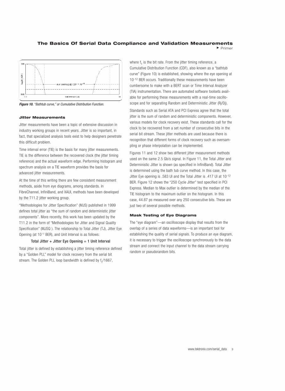
Cumulative Distribution Function (CDF), also known as a “bathtub
curve” (Figure 10) is established, showing where the eye opening at
10-12 BER occurs. Traditionally these measurements have been
cumbersome to make with a BERT scan or Time Interval Analyzer
(TIA) instrumentation. There are automated software toolsets avail-
able for performing these measurements with a real-time oscillo-
scope and for separating Random and Deterministic Jitter (Rj/Dj).
Standards such as Serial ATA and PCI Express agree that the total
jitter is the sum of random and deterministic components. However,
various models for clock recovery exist. These standards call for the
clock to be recovered from a set number of consecutive bits in the
serial bit stream. These jitter methods are used because there is
recognition that different forms of clock recovery such as oversam-
pling or phase interpolation can be implemented.
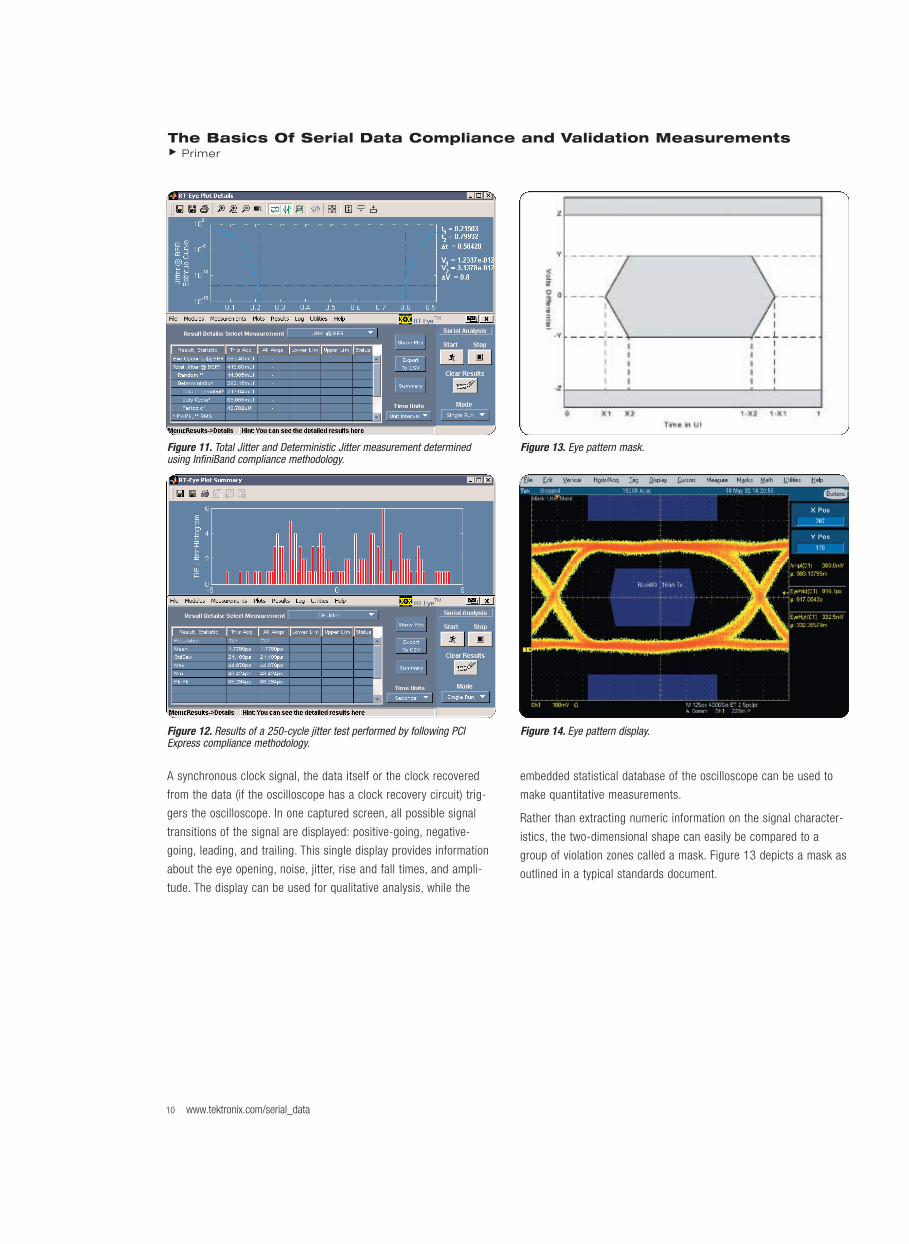
Figures 11 and 12 show two different jitter measurement methods
used on the same 2.5 Gb/s signal. In Figure 11, the Total Jitter and
Deterministic Jitter is shown (as specified in InfiniBand). Total Jitter
is determined using the bath tub curve method. In this case, the
Jitter Eye opening is .583 UI and the Total Jitter is .417 UI at 10-12
BER. Figure 12 shows the “250 Cycle Jitter” test specified in PCI
Express. Median to Max outlier is determined by the median of the
TIE histogram to the maximum outlier on the histogram. In this
case, 44.87 ps measured over any 250 consecutive bits. These are
just two of several possible methods.
Mask Testing of Eye Diagrams
The “eye diagram”—an oscilloscope display that results from the
overlap of a series of data waveforms—is an important tool for
establishing the quality of serial signals. To produce an eye diagram,
it is necessary to trigger the oscilloscope synchronously to the data
stream and connect the input channel to the data stream carrying
random or pseudorandom bits.
9www.tektronix.com/serial_data
Figure 10. “Bathtub curve,” or Cumulative Distribution Function.
The Basics Of Serial Data Compliance and Validation MeasurementsPrimer
A synchronous clock signal, the data itself or the clock recovered
from the data (if the oscilloscope has a clock recovery circuit) trig-
gers the oscilloscope. In one captured screen, all possible signal
transitions of the signal are displayed: positive-going, negative-
going, leading, and trailing. This single display provides information
about the eye opening, noise, jitter, rise and fall times, and ampli-
tude. The display can be used for qualitative analysis, while the
embedded statistical database of the oscilloscope can be used to
make quantitative measurements.
Rather than extracting numeric information on the signal character-
istics, the two-dimensional shape can easily be compared to a
group of violation zones called a mask. Figure 13 depicts a mask as
outlined in a typical standards document.
10 www.tektronix.com/serial_data
Figure 13. Eye pattern mask.
Figure 14. Eye pattern display.
Figure 11. Total Jitter and Deterministic Jitter measurement determinedusing InfiniBand compliance methodology.
Figure 12. Results of a 250-cycle jitter test performed by following PCIExpress compliance methodology.
The Basics Of Serial Data Compliance and Validation MeasurementsPrimer
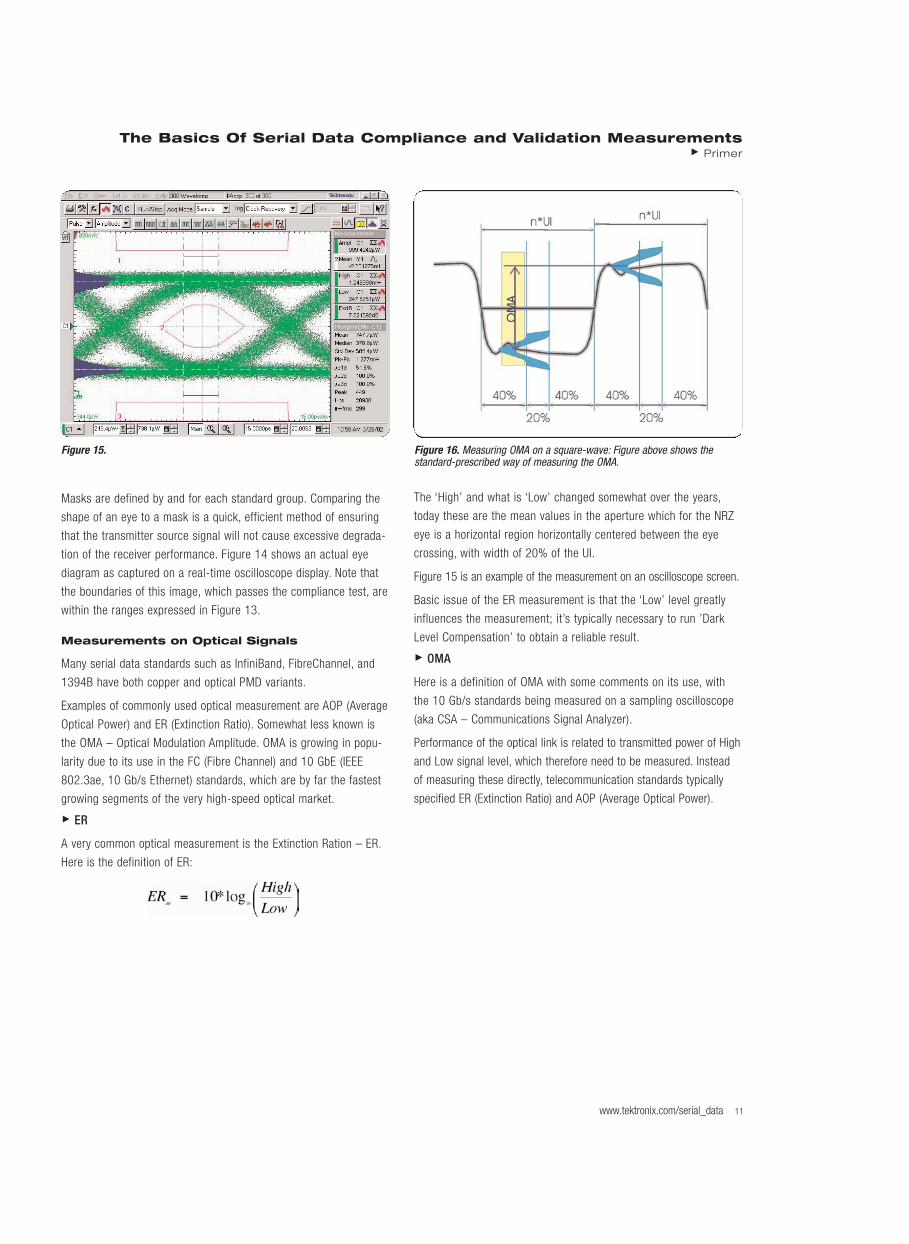
Masks are defined by and for each standard group. Comparing the
shape of an eye to a mask is a quick, efficient method of ensuring
that the transmitter source signal will not cause excessive degrada-
tion of the receiver performance. Figure 14 shows an actual eye
diagram as captured on a real-time oscilloscope display. Note that
the boundaries of this image, which passes the compliance test, are
within the ranges expressed in Figure 13.
Measurements on Optical Signals
Many serial data standards such as InfiniBand, FibreChannel, and
1394B have both copper and optical PMD variants.
Examples of commonly used optical measurement are AOP (Average
Optical Power) and ER (Extinction Ratio). Somewhat less known is
the OMA – Optical Modulation Amplitude. OMA is growing in popu-
larity due to its use in the FC (Fibre Channel) and 10 GbE (IEEE
802.3ae, 10 Gb/s Ethernet) standards, which are by far the fastest
growing segments of the very high-speed optical market.
ER
A very common optical measurement is the Extinction Ration – ER.
Here is the definition of ER:
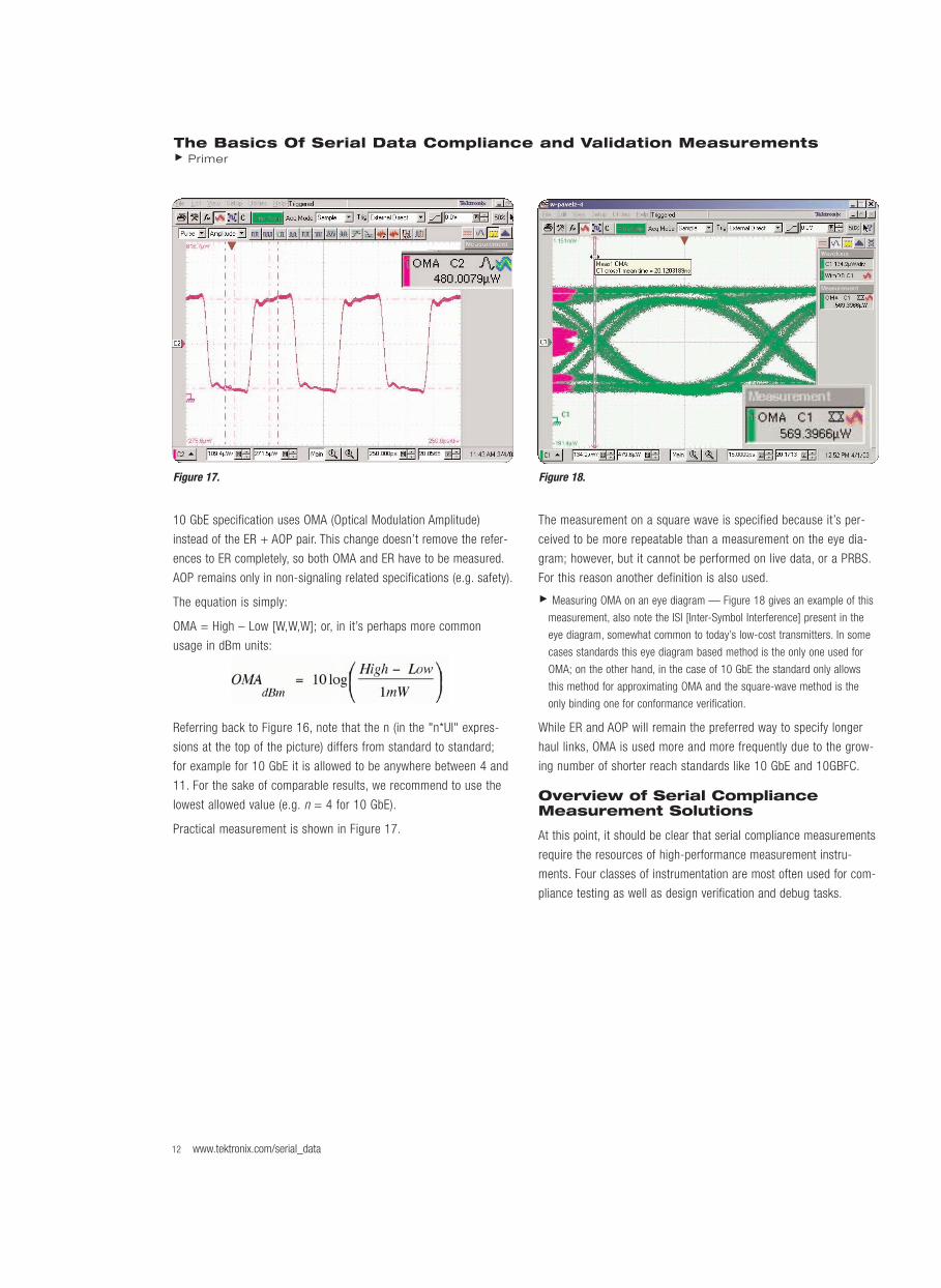
The ‘High’ and what is ‘Low’ changed somewhat over the years,
today these are the mean values in the aperture which for the NRZ
eye is a horizontal region horizontally centered between the eye
crossing, with width of 20% of the UI.
Figure 15 is an example of the measurement on an oscilloscope screen.
Basic issue of the ER measurement is that the ‘Low’ level greatly
influences the measurement; it’s typically necessary to run ’Dark
Level Compensation’ to obtain a reliable result.
OMA
Here is a definition of OMA with some comments on its use, with
the 10 Gb/s standards being measured on a sampling oscilloscope
(aka CSA – Communications Signal Analyzer).
Performance of the optical link is related to transmitted power of High
and Low signal level, which therefore need to be measured. Instead
of measuring these directly, telecommunication standards typically
specified ER (Extinction Ratio) and AOP (Average Optical Power).
11www.tektronix.com/serial_data
Figure 15. Figure 16. Measuring OMA on a square-wave: Figure above shows the standard-prescribed way of measuring the OMA.
The Basics Of Serial Data Compliance and Validation MeasurementsPrimer
10 GbE specification uses OMA (Optical Modulation Amplitude)
instead of the ER + AOP pair. This change doesn’t remove the refer-
ences to ER completely, so both OMA and ER have to be measured.
AOP remains only in non-signaling related specifications (e.g. safety).
The equation is simply:
OMA = High – Low [W,W,W]; or, in it’s perhaps more common
usage in dBm units:
Referring back to Figure 16, note that the n (in the "n*UI" expres-
sions at the top of the picture) differs from standard to standard;
for example for 10 GbE it is allowed to be anywhere between 4 and
11. For the sake of comparable results, we recommend to use the
lowest allowed value (e.g. n = 4 for 10 GbE).
Practical measurement is shown in Figure 17.
The measurement on a square wave is specified because it’s per-
ceived to be more repeatable than a measurement on the eye dia-
gram; however, but it cannot be performed on live data, or a PRBS.
For this reason another definition is also used.
Measuring OMA on an eye diagram — Figure 18 gives an example of this
measurement, also note the ISI [Inter-Symbol Interference] present in the
eye diagram, somewhat common to today’s low-cost transmitters. In some
cases standards this eye diagram based method is the only one used for
OMA; on the other hand, in the case of 10 GbE the standard only allows
this method for approximating OMA and the square-wave method is the
only binding one for conformance verification.
While ER and AOP will remain the preferred way to specify longer
haul links, OMA is used more and more frequently due to the grow-
ing number of shorter reach standards like 10 GbE and 10GBFC.
Overview of Serial ComplianceMeasurement Solutions
At this point, it should be clear that serial compliance measurements
require the resources of high-performance measurement instru-
ments. Four classes of instrumentation are most often used for com-
pliance testing as well as design verification and debug tasks.
12 www.tektronix.com/serial_data
Figure 17. Figure 18.
The Basics Of Serial Data Compliance and Validation MeasurementsPrimer
Real-time Oscilloscopes
The tool of choice for measuring the electrical portion of the PHY is
a high-performance real-time (RT) oscilloscope. State-of-the-art dig-
ital storage oscilloscopes and (DSO) and digital phosphor oscillo-
scopes (DPO) can capture continuous, contiguous data in the multi-
gigabit range with very good signal integrity. Many current-genera-
tion instruments include Digital Signal Processing (DSP) software
algorithms that can recover the embedded clock from a serial data
bit stream acquired with a single trigger event. This eliminates trig-
ger jitter from subsequent analysis steps. Some real-time oscillo-
scopes offer both Real-Time (RT) and Equivalent Time (ET) Eye read-
ing techniques using hardware clock recovery, each of which has
their advantages.
Once a clock is recovered from a serial bit stream, the oscilloscope
can create an eye diagram and a frequency spectrum of the Time
Interval Error (TIE). The TIE can be analyzed to separate random and
deterministic jitter, an analysis that also provides an estimate for
total jitter at the 10-12 bit error rate (BER).
Aside from combining the functions of several instruments into one,
the RT oscilloscope has other advantages: probing flexibility, rich
display, triggering capabilities, and more. The RT oscilloscope
makes an ideal platform for serial data validation, debug, and
compliance testing.
Sampling Oscilloscopes
The only oscilloscopes available for looking at very high-speed analog
signal integrity are high-speed sampling oscilloscopes. With a maxi-
mum bandwidth of 70+ GHz, these instruments are capable of ana-
lyzing optical and electrical signals at 40 GBp/s and beyond.
Sampling oscilloscopes capture waveforms in “Equivalent Time“ (ET),
constructing a composite image from samples accumulated over
numerous repetitive cycles. Waveform eye diagrams created by sam-
pling oscilloscopes provide a good view of optical and electrical signal
characteristics. An extensive library of built-in measurements makes
this the ideal tool for characterization and compliance testing of very
high-speed components, transceivers, and transmission systems.
Logic Analyzers
The preferred tool for measuring the formatted serial data (as opposed
to individual pulse characteristics) is the logic analyzer. Unlike both RT
and ET oscilloscopes, logic analyzers capture binary data and express
it in terms of clocks, cycles, and edge transitions. The purpose of the
logic analyzer is to simplify acquisition and analysis of the purely digi-
tal aspects of the serial transmission. To carry out its serial bus debug
mission, it must deliver features consistent with the needs of high-
speed buses: high sample rate, deep memory, flexible triggering and
synchronization, and more. And like the oscilloscope, it must offer low-
impact probing tools.
Signal Sources
Good high-speed engineering practices include exercising designs under
“real-world” conditions. The right tool for mimicking these conditions as
closely as possible is a programmable signal source. Generating test
signals at today's data rates requires high-speed Data Timing
Generators (DTG) and Arbitrary Waveform Generators (AWG). Without
these instruments there would be no way to test and validate new physi-
cal layer designs. Many signal sources can replay signals that have been
captured with an oscilloscope. The signals can act as a reference signal
or may be modified to stress the device under test.
Data Timing Generators are especially useful for generating multiple
streams of channels of parallel data—up to 96 channels in today’s
most advanced instruments. These tools deliver 3.3 Gb/s data rates,
sufficient to cover most of today's standards. At the same time
these advanced instruments provide a host of signal manipulation
features including independent level, rise/fall and jitter controls.
High-speed digital signals inevitably have analog attributes. Arbitrary
Waveform Generators can provide stimulus signals with analog content
(usually deliberate impairments) on a bus channel. Capable of deliver-
ing any type or shape of waveform, AWGs are universally applied in
design and manufacturing. Current AWGs have sample rates exceeding
4 GS/s (2 GHz bandwidth), equivalent to a 4 Gb/s data rate.
13www.tektronix.com/serial_data
The Basics Of Serial Data Compliance and Validation MeasurementsPrimer
Of these four tools, the real-time oscilloscope has become the work-
horse of compliance testing. It also serves as a debug troubleshoot-
ing platform, where it is assisted by the logic analyzer. Recent
advances in both measurement performance and integrated analysis
capability have made the RT oscilloscope the choice of standards
groups, product developers, and compliance certification providers.
Analog Compliance MeasurementConsiderations: Probing
Every serial measurement, whether for compliance testing, valida-
tion, or troubleshooting purposes, consists of probing the device,
acquiring the signal data, and analyzing the captured information.
Selecting the right tools, and applying them correctly, is the way to
ensure fast, accurate results. The balance of this document will deal
with the measurement needs of today’s high-speed serial devices.
Connecting to the Serial Device Under Test
Measurements begin with a connection to the device under test. In
the case of serial bus architectures, the question arises: what is the
mechanical interface of the lane to be tested? This is a question
usually answered in the mechanical portion of the standard, some-
times called the physical media dependent (PMD) specification. There
are diverse configurations, each with its own unique characteristics.
The mechanical interface has a profound impact on probing for both
electrical and logical testing. The probe may need to match tiny
physical features, while delivering high-speed differential signals
intact to the measurement instrument. Alternatively, the probe may
need to adapt to prototype fixturing such as test points fitted with
SMA connectors.
There are four approaches to the probing challenge. Remember, the
signals in most serial architectures are transmitted differentially, so
all of the solutions explained here are meant to connect differentially.
Pseudo-Differentially Connected Movable Probes — Compliance measure-
ments usually have specified test points, but troubleshooting work may
require probing circuit points anywhere on a device’s circuit board. This
makes it necessary to probe individual circuit traces and pins with move-
able manual probes. Both pseudo-differential and true differential probing
solutions are available. Both configurations have their strengths.
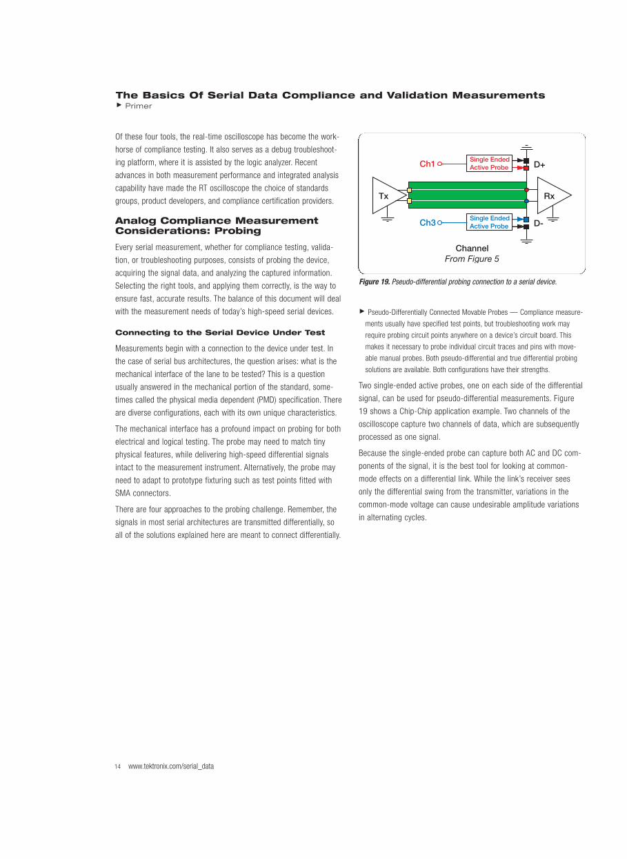
Two single-ended active probes, one on each side of the differential
signal, can be used for pseudo-differential measurements. Figure
19 shows a Chip-Chip application example. Two channels of the
oscilloscope capture two channels of data, which are subsequently
processed as one signal.
Because the single-ended probe can capture both AC and DC com-
ponents of the signal, it is the best tool for looking at common-
mode effects on a differential link. While the link’s receiver sees
only the differential swing from the transmitter, variations in the
common-mode voltage can cause undesirable amplitude variations
in alternating cycles.
14 www.tektronix.com/serial_data
Tx
ChannelFrom Figure 5
D+Ch1
Rx
Single EndedActive Probe
D-Ch3Single EndedActive Probe
Figure 19. Pseudo-differential probing connection to a serial device.
The Basics Of Serial Data Compliance and Validation MeasurementsPrimer
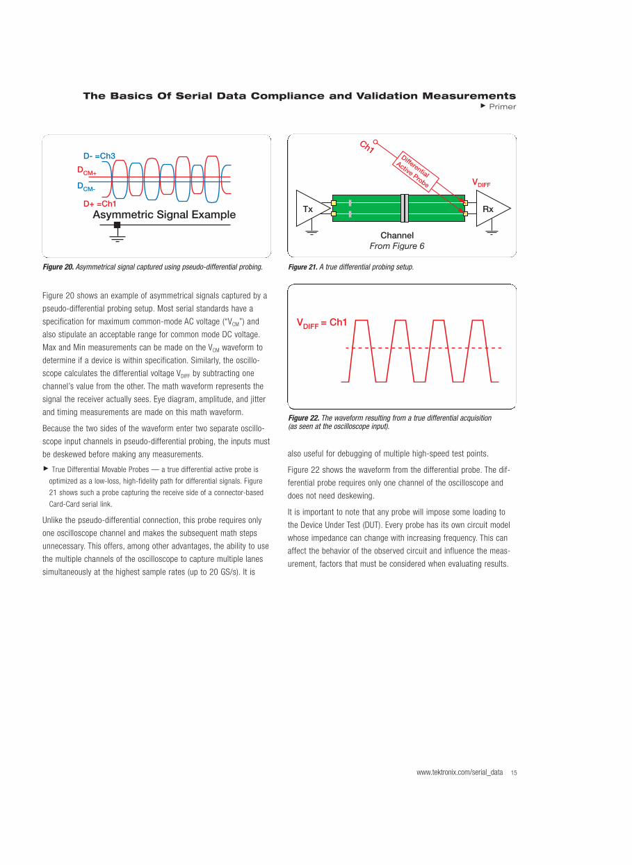
Figure 20 shows an example of asymmetrical signals captured by a
pseudo-differential probing setup. Most serial standards have a
specification for maximum common-mode AC voltage (“VCM”) and
also stipulate an acceptable range for common mode DC voltage.
Max and Min measurements can be made on the VCM waveform to
determine if a device is within specification. Similarly, the oscillo-
scope calculates the differential voltage VDIFF by subtracting one
channel’s value from the other. The math waveform represents the
signal the receiver actually sees. Eye diagram, amplitude, and jitter
and timing measurements are made on this math waveform.
Because the two sides of the waveform enter two separate oscillo-
scope input channels in pseudo-differential probing, the inputs must
be deskewed before making any measurements.
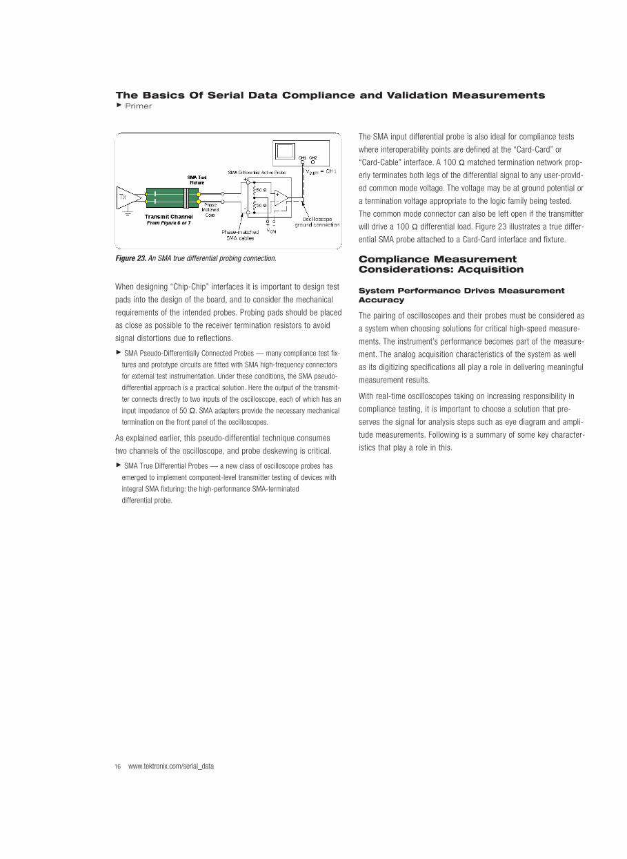
True Differential Movable Probes — a true differential active probe is
optimized as a low-loss, high-fidelity path for differential signals. Figure
21 shows such a probe capturing the receive side of a connector-based
Card-Card serial link.
Unlike the pseudo-differential connection, this probe requires only
one oscilloscope channel and makes the subsequent math steps
unnecessary. This offers, among other advantages, the ability to use
the multiple channels of the oscilloscope to capture multiple lanes
simultaneously at the highest sample rates (up to 20 GS/s). It is
also useful for debugging of multiple high-speed test points.
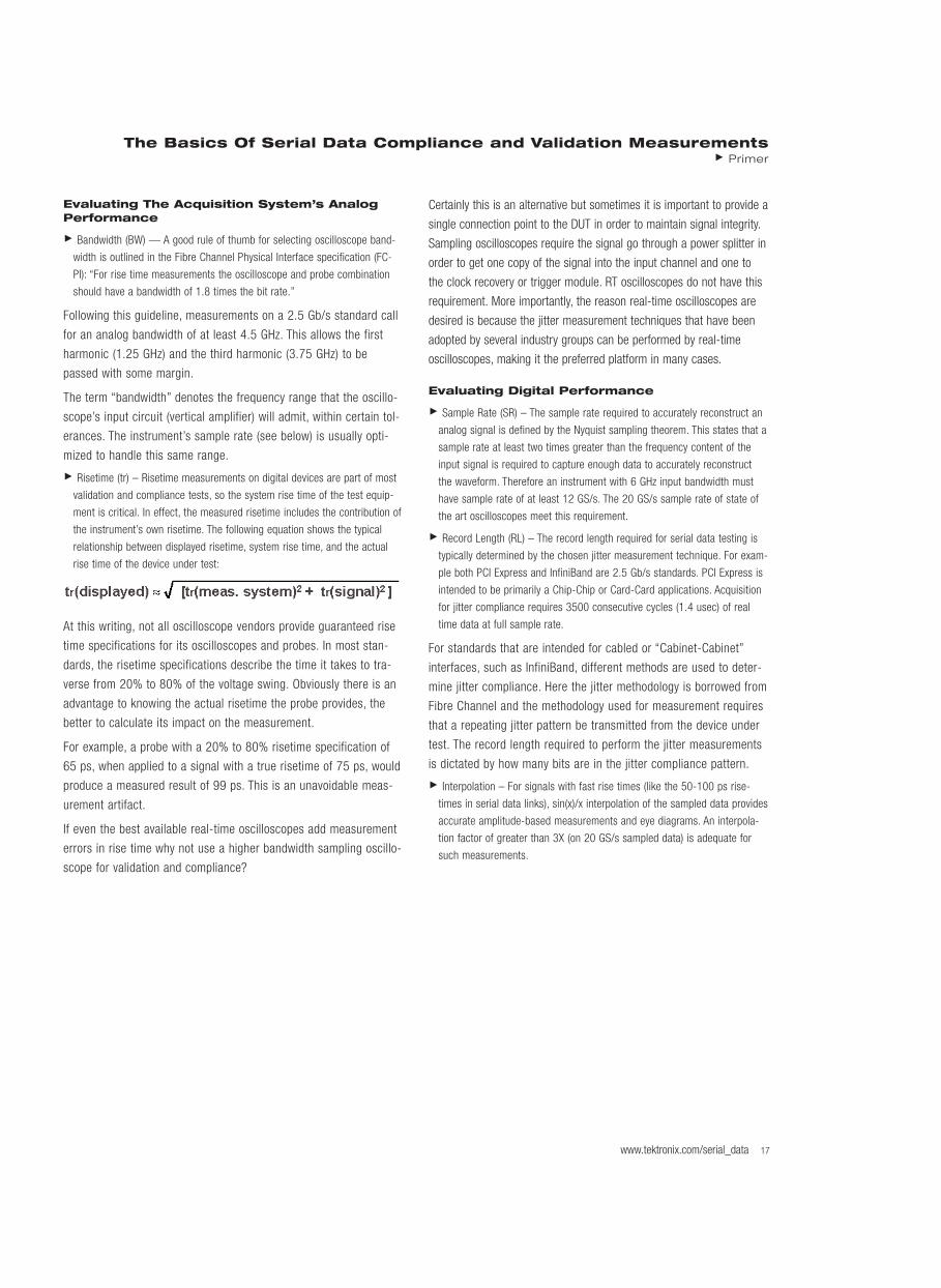
Figure 22 shows the waveform from the differential probe. The dif-
ferential probe requires only one channel of the oscilloscope and
does not need deskewing.
It is important to note that any probe will impose some loading to
the Device Under Test (DUT). Every probe has its own circuit model
whose impedance can change with increasing frequency. This can
affect the behavior of the observed circuit and influence the meas-
urement, factors that must be considered when evaluating results.
15www.tektronix.com/serial_data
Asymmetric Signal Example
D- =Ch3
D+ =Ch1
DCM+
DCM-
Figure 20. Asymmetrical signal captured using pseudo-differential probing.
Tx
ChannelFrom Figure 6
Ch1
VDIFF
Rx
Differential
Active Probe
Figure 21. A true differential probing setup.
VDIFF = Ch1
Figure 22. The waveform resulting from a true differential acquisition (as seen at the oscilloscope input).
The Basics Of Serial Data Compliance and Validation MeasurementsPrimer
When designing “Chip-Chip” interfaces it is important to design test
pads into the design of the board, and to consider the mechanical
requirements of the intended probes. Probing pads should be placed
as close as possible to the receiver termination resistors to avoid
signal distortions due to reflections.
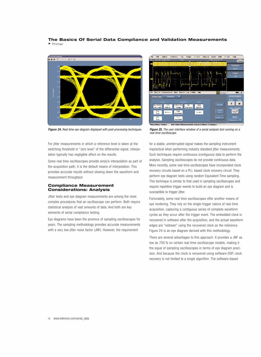
SMA Pseudo-Differentially Connected Probes — many compliance test fix-
tures and prototype circuits are fitted with SMA high-frequency connectors
for external test instrumentation. Under these conditions, the SMA pseudo-
differential approach is a practical solution. Here the output of the transmit-
ter connects directly to two inputs of the oscilloscope, each of which has an
input impedance of 50 Ω. SMA adapters provide the necessary mechanical
termination on the front panel of the oscilloscopes.
As explained earlier, this pseudo-differential technique consumes
two channels of the oscilloscope, and probe deskewing is critical.
SMA True Differential Probes — a new class of oscilloscope probes has
emerged to implement component-level transmitter testing of devices with
integral SMA fixturing: the high-performance SMA-terminated
differential probe.
The SMA input differential probe is also ideal for compliance tests
where interoperability points are defined at the “Card-Card” or
“Card-Cable” interface. A 100 Ω matched termination network prop-
erly terminates both legs of the differential signal to any user-provid-
ed common mode voltage. The voltage may be at ground potential or
a termination voltage appropriate to the logic family being tested.
The common mode connector can also be left open if the transmitter
will drive a 100 Ω differential load. Figure 23 illustrates a true differ-
ential SMA probe attached to a Card-Card interface and fixture.
Compliance MeasurementConsiderations: Acquisition
System Performance Drives MeasurementAccuracy
The pairing of oscilloscopes and their probes must be considered as
a system when choosing solutions for critical high-speed measure-
ments. The instrument’s performance becomes part of the measure-
ment. The analog acquisition characteristics of the system as well
as its digitizing specifications all play a role in delivering meaningful
measurement results.
With real-time oscilloscopes taking on increasing responsibility in
compliance testing, it is important to choose a solution that pre-
serves the signal for analysis steps such as eye diagram and ampli-
tude measurements. Following is a summary of some key character-
istics that play a role in this.
16 www.tektronix.com/serial_data
Figure 23. An SMA true differential probing connection.
The Basics Of Serial Data Compliance and Validation MeasurementsPrimer
Evaluating The Acquisition System’s AnalogPerformance
Bandwidth (BW) — A good rule of thumb for selecting oscilloscope band-
width is outlined in the Fibre Channel Physical Interface specification (FC-
PI): “For rise time measurements the oscilloscope and probe combination
should have a bandwidth of 1.8 times the bit rate.”
Following this guideline, measurements on a 2.5 Gb/s standard call
for an analog bandwidth of at least 4.5 GHz. This allows the first
harmonic (1.25 GHz) and the third harmonic (3.75 GHz) to be
passed with some margin.
The term “bandwidth” denotes the frequency range that the oscillo-
scope’s input circuit (vertical amplifier) will admit, within certain tol-
erances. The instrument’s sample rate (see below) is usually opti-
mized to handle this same range.
Risetime (tr) – Risetime measurements on digital devices are part of most
validation and compliance tests, so the system rise time of the test equip-
ment is critical. In effect, the measured risetime includes the contribution of
the instrument’s own risetime. The following equation shows the typical
relationship between displayed risetime, system rise time, and the actual
rise time of the device under test:
At this writing, not all oscilloscope vendors provide guaranteed rise
time specifications for its oscilloscopes and probes. In most stan-
dards, the risetime specifications describe the time it takes to tra-
verse from 20% to 80% of the voltage swing. Obviously there is an
advantage to knowing the actual risetime the probe provides, the
better to calculate its impact on the measurement.
For example, a probe with a 20% to 80% risetime specification of
65 ps, when applied to a signal with a true risetime of 75 ps, would
produce a measured result of 99 ps. This is an unavoidable meas-
urement artifact.
If even the best available real-time oscilloscopes add measurement
errors in rise time why not use a higher bandwidth sampling oscillo-
scope for validation and compliance?
Certainly this is an alternative but sometimes it is important to provide a
single connection point to the DUT in order to maintain signal integrity.
Sampling oscilloscopes require the signal go through a power splitter in
order to get one copy of the signal into the input channel and one to
the clock recovery or trigger module. RT oscilloscopes do not have this
requirement. More importantly, the reason real-time oscilloscopes are
desired is because the jitter measurement techniques that have been
adopted by several industry groups can be performed by real-time
oscilloscopes, making it the preferred platform in many cases.
Evaluating Digital Performance
Sample Rate (SR) – The sample rate required to accurately reconstruct an
analog signal is defined by the Nyquist sampling theorem. This states that a
sample rate at least two times greater than the frequency content of the
input signal is required to capture enough data to accurately reconstruct
the waveform. Therefore an instrument with 6 GHz input bandwidth must
have sample rate of at least 12 GS/s. The 20 GS/s sample rate of state of
the art oscilloscopes meet this requirement.
Record Length (RL) – The record length required for serial data testing is
typically determined by the chosen jitter measurement technique. For exam-
ple both PCI Express and InfiniBand are 2.5 Gb/s standards. PCI Express is
intended to be primarily a Chip-Chip or Card-Card applications. Acquisition
for jitter compliance requires 3500 consecutive cycles (1.4 usec) of real
time data at full sample rate.
For standards that are intended for cabled or “Cabinet-Cabinet”
interfaces, such as InfiniBand, different methods are used to deter-
mine jitter compliance. Here the jitter methodology is borrowed from
Fibre Channel and the methodology used for measurement requires
that a repeating jitter pattern be transmitted from the device under
test. The record length required to perform the jitter measurements
is dictated by how many bits are in the jitter compliance pattern.
Interpolation – For signals with fast rise times (like the 50-100 ps rise-
times in serial data links), sin(x)/x interpolation of the sampled data provides
accurate amplitude-based measurements and eye diagrams. An interpola-
tion factor of greater than 3X (on 20 GS/s sampled data) is adequate for
such measurements.
17www.tektronix.com/serial_data
The Basics Of Serial Data Compliance and Validation MeasurementsPrimer
For jitter measurements in which a reference level is taken at the
switching threshold or “zero level” of the differential signal, interpo-
lation typically has negligible affect on the results.
Some real time oscilloscopes provide sin(x)/x interpolation as part of
the acquisition path; it is the default means of interpolation. This
provides accurate results without slowing down the waveform and
measurement throughput.
Compliance MeasurementConsiderations: Analysis
Jitter tests and eye diagram measurements are among the most
complex procedures that an oscilloscope can perform. Both require
statistical analysis of vast amounts of data. And both are key
elements of serial compliance testing.
Eye diagrams have been the province of sampling oscilloscopes for
years. The sampling methodology provides accurate measurements
with a very low jitter noise factor (JNF). However, the requirement
for a stable, uninterrupted signal makes the sampling instrument
impractical when performing industry standard jitter measurements.
Such techniques require continuous (contiguous) data to perform the
analysis. Sampling oscilloscopes do not provide continuous data.
More recently, some real-time oscilloscopes have incorporated clock
recovery circuits based on a PLL based clock recovery circuit. They
perform eye diagram tests using random Equivalent Time sampling.
This technique is similar to that used in sampling oscilloscopes and
require repetitive trigger events to build an eye diagram and is
susceptible to trigger jitter.
Fortunately, some real-time oscilloscopes offer another means of
eye rendering. They rely on the single-trigger nature of real-time
acquisition, capturing a contiguous series of complete waveform
cycles as they occur after the trigger event. The embedded clock is
recovered in software after the acquisition, and the actual waveform
edges are “redrawn” using the recovered clock as the reference.
Figure 24 is an eye diagram derived with this methodology.
There are several advantages to this approach. It provides a JNF as
low as 700 fs on certain real-time oscilloscope models, making it
the equal of sampling oscilloscopes in terms of eye diagram preci-
sion. And because the clock is recovered using software DSP, clock
recovery is not limited to a single algorithm. The software-based
18 www.tektronix.com/serial_data
Figure 24. Real-time eye diagram displayed with post-processing techniques. Figure 25. The user interface window of a serial analysis tool running on areal-time oscilloscope.
The Basics Of Serial Data Compliance and Validation MeasurementsPrimer
package provides an interface for changing the method by which
the clock is recovered, a valuable asset in a world of constantly
evolving standards. Real-time clock recovery and eye rendering also
provides a means for separating transition bits from non-transition
bits and performing separate mask testing operations on each type
of bit as is required for PCI Express. Figure 27 shows the separation
of Transition and Non-Transition bits from the eye diagram shown in
Figure 24.
It is often necessary to more deeply analyze the data in the context
of the compliance measurements. For example, an eye diagram test
may fail because the embedded clock signal has too much modula-
tion. The eye diagram shows only violations to the mask, but a TIE
waveform trend or frequency spectrum can reveal further clues.
Other built-in oscilloscope tools such as cursor measurements and
zoom controls can aid the in-depth analysis.
Getting a Handle on all that Data
Eye diagrams and jitter measurements in particular produce a vol-
ume of data that would be difficult to manage without the help of
automated analysis tools. Figure 25 shows the user interface of an
integrated analysis package running on a real-time oscilloscope.
Key measurements such as rise and fall time can be set up with
just one on-screen “button.” The acquisition window presents the
raw serial waveform.
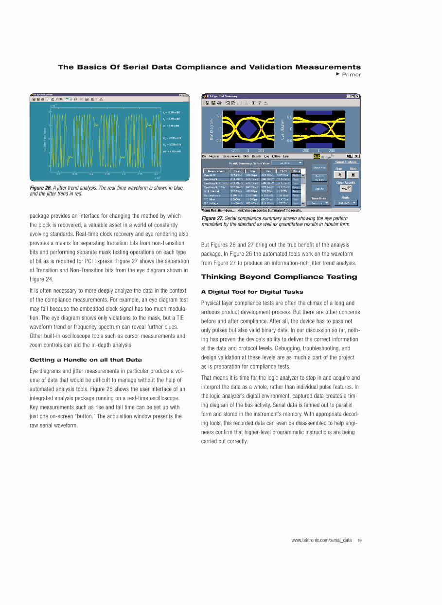
But Figures 26 and 27 bring out the true benefit of the analysis
package. In Figure 26 the automated tools work on the waveform
from Figure 27 to produce an information-rich jitter trend analysis.
Thinking Beyond Compliance Testing
A Digital Tool for Digital Tasks
Physical layer compliance tests are often the climax of a long and
arduous product development process. But there are other concerns
before and after compliance. After all, the device has to pass not
only pulses but also valid binary data. In our discussion so far, noth-
ing has proven the device’s ability to deliver the correct information
at the data and protocol levels. Debugging, troubleshooting, and
design validation at these levels are as much a part of the project
as is preparation for compliance tests.
That means it is time for the logic analyzer to step in and acquire and
interpret the data as a whole, rather than individual pulse features. In
the logic analyzer’s digital environment, captured data creates a tim-
ing diagram of the bus activity. Serial data is fanned out to parallel
form and stored in the instrument’s memory. With appropriate decod-
ing tools, this recorded data can even be disassembled to help engi-
neers confirm that higher-level programmatic instructions are being
carried out correctly.
19www.tektronix.com/serial_data
Figure 26. A jitter trend analysis. The real-time waveform is shown in blue,and the jitter trend in red.
Figure 27. Serial compliance summary screen showing the eye pattern mandated by the standard as well as quantitative results in tabular form.
The Basics Of Serial Data Compliance and Validation MeasurementsPrimer
While this document deals mainly with analog compliance test chal-
lenges and solutions, it is worthwhile to review the logic analyzer
systems that supplement real-time and sampling oscilloscopes for
serial measurements.
Probing Means Making the Right Connections
All measurements start with probing, and preserving signal fidelity is
just as much a concern here as it was with the analog acquisition.
Earlier we discussed the practice of fixturing prototype devices with
SMA connectors to deliver maximum signal fidelity to an oscillo-
scope. Logic analyzers have their own answer to this approach, with
the same signal fidelity objectives in mind.
At frequencies of 2.5 Gb/s and higher, it is not enough to simply clip
on a common logic analyzer probe. Flying leads and micrograbbers
will introduce ground loops and other unpredictable analog effects.
Even routing signals to pin headers will impact low-voltage, high-
frequency serial signals. They simply will not tolerate the electrical
stub or the loss contributed by a connector.
Instead, a probing method must be considered during board layout.
The preferred method for serial signals such as PCI Express is to
route the traces to a landing pad. Unlike a connector-based access
point, a landing pad has almost no impact on the signal when probe
is not in use. Of course, a landing pad requires a matching pattern
on the logic analyzer probe.
Clearly the goal is to minimize the loading effect of the probe. But
any probe will contribute to the signal loss budget. High-speed sig-
nals are sensitive to the impedance of the probe, particularly its
capacitive load. As the bandwidth of a signal increases, so does the
effect of the probe capacitance. The “ideal” probe for serial bus
acquisition has:
High analog bandwidth
High impedance
Low capacitance
Minimal stub
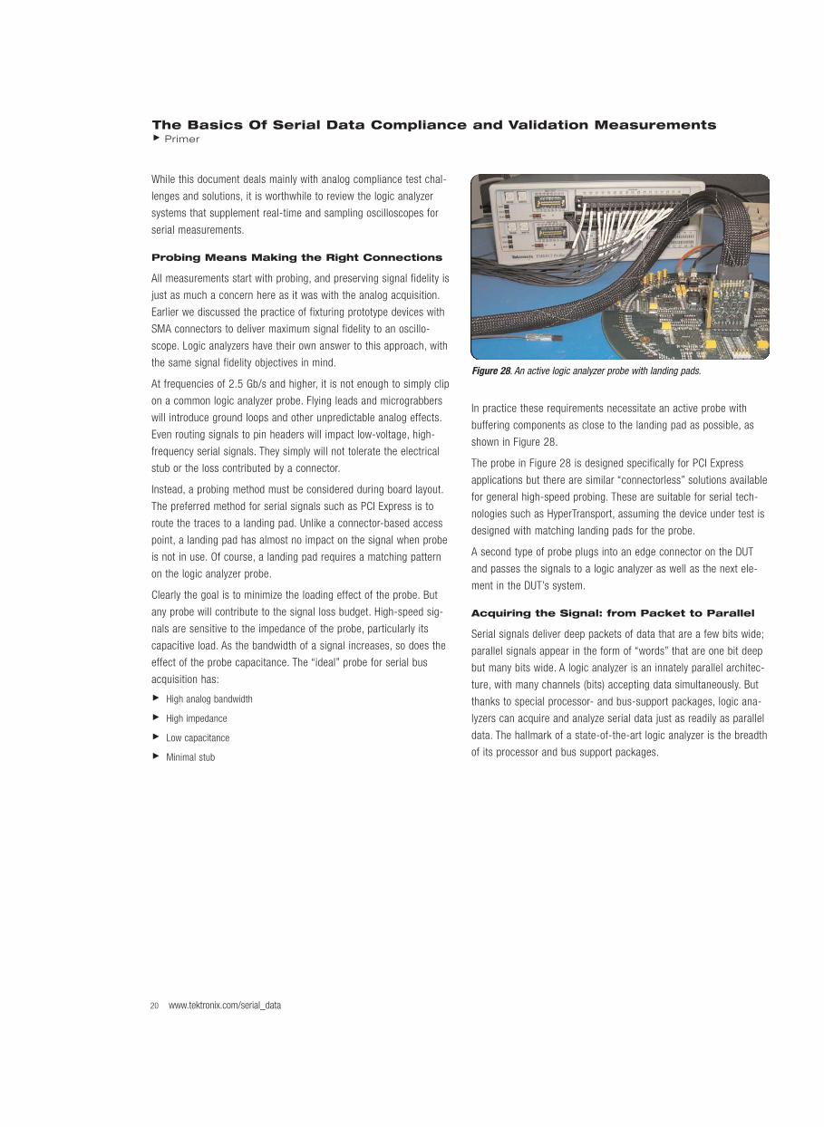
In practice these requirements necessitate an active probe with
buffering components as close to the landing pad as possible, as
shown in Figure 28.
The probe in Figure 28 is designed specifically for PCI Express
applications but there are similar “connectorless” solutions available
for general high-speed probing. These are suitable for serial tech-
nologies such as HyperTransport, assuming the device under test is
designed with matching landing pads for the probe.
A second type of probe plugs into an edge connector on the DUT
and passes the signals to a logic analyzer as well as the next ele-
ment in the DUT’s system.
Acquiring the Signal: from Packet to Parallel
Serial signals deliver deep packets of data that are a few bits wide;
parallel signals appear in the form of “words” that are one bit deep
but many bits wide. A logic analyzer is an innately parallel architec-
ture, with many channels (bits) accepting data simultaneously. But
thanks to special processor- and bus-support packages, logic ana-
lyzers can acquire and analyze serial data just as readily as parallel
data. The hallmark of a state-of-the-art logic analyzer is the breadth
of its processor and bus support packages.
20 www.tektronix.com/serial_data
Figure 28. An active logic analyzer probe with landing pads.
The Basics Of Serial Data Compliance and Validation MeasurementsPrimer
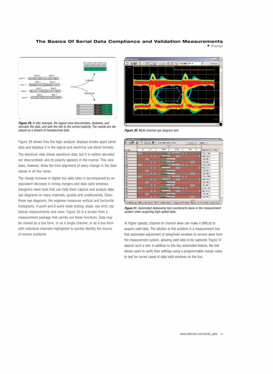
Figure 29 shows how the logic analyzer displays breaks apart serial
data and displays it in the logical and electrical sub-block formats.
The electrical view shows waveform data, but it is neither decoded
nor descrambled, and its polarity appears in the inverse. This view
does, however, show the time alignment of every change in the data
values in all four lanes.
The steady increase in digital bus data rates is accompanied by an
equivalent decrease in timing margins and data-valid windows.
Designers need tools that can help them capture and analyze data
eye diagrams on many channels, quickly and unobtrusively. Given
these eye diagrams, the engineer measures vertical and horizontal
histograms, 4-point and 6-point mask testing, slope, eye-limit, sta-
tistical measurements and more. Figure 30 is a screen from a
measurement package that carries out these functions. Data may
be viewed as a bus form, or as a single channel, or as a bus form
with individual channels highlighted to quickly identify the source
of elusive problems.
At higher speeds, channel-to-channel skew can make it difficult to
acquire valid data. The solution to this problem is a measurement tool
that automates adjustment of setup/hold windows to remove skew from
the measurement system, allowing valid data to be captured. Figure 31
depicts such a tool. In addition to this key automated feature, the tool
allows users to verify their settings using a programmable margin value
to test for corner cases of data valid windows on the bus.
21www.tektronix.com/serial_data
Figure 29. In this example, the logical view descrambles, deskews, anddecodes the data, and sets the bits to the correct polarity. The results are dis-played as a stream of hexadecimal data. Figure 30. Multi-channel eye diagram tool.
Figure 31. Automated deskewing tool counteracts skew in the measurementsystem when acquiring high-speed data.
The Basics Of Serial Data Compliance and Validation MeasurementsPrimer
These tools are important part of the troubleshooting process. They
make it possible to spot errors and begin the process of tracing
backward toward the causes. Some logic analyzers can interface
directly to an oscilloscope as well, displaying the oscilloscope’s
waveform view in perfect time correlation with the logical or electri-
cal displays. This simplifies troubleshooting of problems that arise
from signal integrity defects, for example.
Triggering is the Key to Efficiency inTroubleshooting
One of the defining features of any logic analyzer is the flexibility of
its triggering system. When coupled with a support package
designed for a particular serial standard (such as RapidIO or PCI
Express), the logic analyzer delivers advanced triggering capabilities
to easily isolate and capture specified transactions.
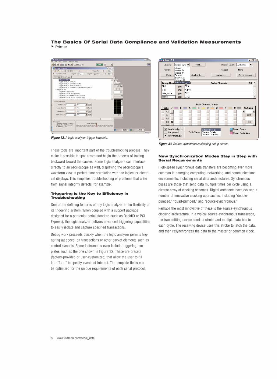
Debug work proceeds quickly when the logic analyzer permits trig-
gering (at speed) on transactions or other packet elements such as
control symbols. Some instruments even include triggering tem-
plates such as the one shown in Figure 32. These are presets
(factory-provided or user-customized) that allow the user to fill
in a “form” to specify events of interest. The template fields can
be optimized for the unique requirements of each serial protocol.
New Synchronization Modes Stay in Step withSerial Requirements
High-speed synchronous data transfers are becoming ever more
common in emerging computing, networking, and communications
environments, including serial data architectures. Synchronous
buses are those that send data multiple times per cycle using a
diverse array of clocking schemes. Digital architects have devised a
number of innovative clocking approaches, including “double-
pumped,” “quad-pumped,” and “source-synchronous.”
Perhaps the most innovative of these is the source-synchronous
clocking architecture. In a typical source-synchronous transaction,
the transmitting device sends a strobe and multiple data bits in
each cycle. The receiving device uses this strobe to latch the data,
and then resynchronizes the data to the master or common clock.
22 www.tektronix.com/serial_data
Figure 33. Source-synchronous clocking setup screen.
Figure 32. A logic analyzer trigger template.
The Basics Of Serial Data Compliance and Validation MeasurementsPrimer
In a HyperTransport link, for example, commands, addresses, and
data transfers are source-synchronous as well as “double-pumped.”
Packet transfers take place on both the rising and falling edges of the
clock signal, yielding a data rate twice that of the clock frequency.
Complex synchronous clocking schemes that deliver multiple bits in
every cycle can only continue to grow in popularity, as developers
strive for ever-higher bandwidths in their digital systems. Logic ana-
lyzers must keep pace with this trend. Today, some instruments
offer simplified control of synchronous acquisition, again using
setup steps involving self-explanatory templates such as the one
shown in Figure 33.
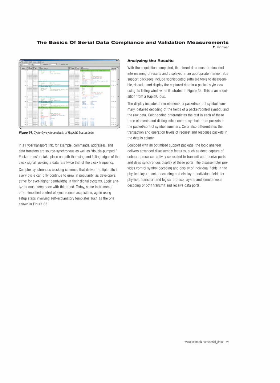
Analyzing the Results
With the acquisition completed, the stored data must be decoded
into meaningful results and displayed in an appropriate manner. Bus
support packages include sophisticated software tools to disassem-
ble, decode, and display the captured data in a packet-style view
using its listing window, as illustrated in Figure 34. This is an acqui-
sition from a RapidIO bus.
The display includes three elements: a packet/control symbol sum-
mary, detailed decoding of the fields of a packet/control symbol, and
the raw data. Color-coding differentiates the text in each of these
three elements and distinguishes control symbols from packets in
the packet/control symbol summary. Color also differentiates the
transaction and operation levels of request and response packets in
the details column.
Equipped with an optimized support package, the logic analyzer
delivers advanced disassembly features, such as deep capture of
onboard processor activity correlated to transmit and receive ports
and deep synchronous display of these ports. The disassembler pro-
vides control symbol decoding and display of individual fields in the
physical layer; packet decoding and display of individual fields for
physical, transport and logical protocol layers; and simultaneous
decoding of both transmit and receive data ports.
23www.tektronix.com/serial_data
Figure 34. Cycle-by-cycle analysis of RapidIO bus activity.
For Further InformationTektronix maintains a comprehensive, constantly expanding collec-tion of application notes, technical briefs and other resources to helpengineers working on the cutting edge of technology. Please visitwww.tektronix.com
24 www.tektronix.com/serial_data
Summary
Serial buses, components, and transmission elements are here to
stay, and are destined to grow in importance as technology markets
continue to demand ever-accelerating data rates. Design and
validation engineers have a new and perhaps unfamiliar discipline—
serial compliance measurement—to learn even as they confront
aggressive development schedules and fast-changing standards.
Fortunately, industry working groups and standards committees have
formed around each of the many serial standards, stabilizing the
technologies and disseminating information about design, architec-
ture, and compliance requirements.
At the same time, a new generation of measurement tools, ranging from
real-time oscilloscopes to logic analyzers and signal sources, has emerged
to help engineers deal with serial measurement challenges. These
solutions deliver the performance to capture, display, and analyze the
most complex serial signals. Thanks to these innovative, automated tools,
engineers can perform serial compliance and validation tests with the
same ease and accuracy as any other measurement.
Copyright © 2003, Tektronix, Inc. All rights reserved. Tektronix products are covered by U.S. and foreign patents, issued and pending. Information in this publication supersedes that in all previously published material. Specification and price change privileges reserved. TEKTRONIX and TEK are registered trademarks of Tektronix, Inc. All other trade names referenced are the service marks,trademarks or registered trademarks of their respective companies.06/03 MD/SFI 55W-16736-0
Contact Tektronix:
ASEAN / Australasia / Pakistan (65) 6356 3900
Austria +43 2236 8092 262
Belgium +32 (2) 715 89 70
Brazil & South America 55 (11) 3741-8360
Canada 1 (800) 661-5625
Central Europe & Greece +43 2236 8092 301
Denmark +45 44 850 700
Finland +358 (9) 4783 400
France & North Africa +33 (0) 1 69 86 80 34
Germany +49 (221) 94 77 400
Hong Kong (852) 2585-6688
India (91) 80-2275577
Italy +39 (02) 25086 1
Japan 81 (3) 3448-3010
Mexico, Central America & Caribbean 52 (55) 56666-333
The Netherlands +31 (0) 23 569 5555
Norway +47 22 07 07 00
People’s Republic of China 86 (10) 6235 1230
Poland +48 (0) 22 521 53 40
Republic of Korea 82 (2) 528-5299
Russia, CIS & The Baltics +358 (9) 4783 400
South Africa +27 11 254 8360
Spain +34 (91) 372 6055
Sweden +46 8 477 6503/4
Taiwan 886 (2) 2722-9622
United Kingdom & Eire +44 (0) 1344 392400
USA 1 (800) 426-2200
USA (Export Sales) 1 (503) 627-1916
For other areas contact Tektronix, Inc. at: 1 (503) 627-7111
Updated 20 September 2002
P7350 and P7350SMADifferential Probes
The P7350 and P7350SMA are your high bandwidth
differential probing solutions for analog validation and
compliance testing, whether probing at the circuit board
or using SMA connection. All the TekConnect.
TDSRT-EYE
TDSRT-EYE Serial Data Compliance and Analysis Software
takes the guesswork out of compliance testing by providing
a complete solution from probe tip to compliance report for
emerging copper serial data standards.


![D122 E N CorelAppli - Corel Corporation and the Canon Validation ID. Click [Sign In]. • The Canon Validation ID is the camcorder’s serial number. To find its location, refer to](https://img.pdfslide.us/doc/110x75/5ab474a57f8b9adc638c1882/d122-e-n-corelappli-corel-and-the-canon-validation-id-click-sign-in-the.jpg)