Embed Size (px)
Citation preview
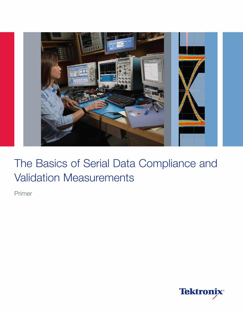
The Basics of Serial Data Compliance andValidation MeasurementsPrimer
Primer
2 www.tektronix.com/serial_data

The Basics of Serial Data Compliance and Validation Measurements
Table of Contents
Serial Buses - An Established Design Standard . . . . . . . . . . . . . . . . . . . . . . . . . . . . . .4
A Range of Serial Standards . . . . . . . . . . . . . . . . .4 - 9 SATA/SAS . . . . . . . . . . . . . . . . . . . . . . . . . . . . . . . . . . .4PCI Express® . . . . . . . . . . . . . . . . . . . . . . . . . . . . . . . . .6Ethernet . . . . . . . . . . . . . . . . . . . . . . . . . . . . . . . . . . . . .6USB . . . . . . . . . . . . . . . . . . . . . . . . . . . . . . . . . . . . . . . .7HDMI/DisplayPort . . . . . . . . . . . . . . . . . . . . . . . . . . . . . .7Common Architectural Elements . . . . . . . . . . . . . . . . . .8
Differential Transmission . . . . . . . . . . . . . . . . . . . . . . .88b/10b Signal Encoding . . . . . . . . . . . . . . . . . . . . . . .8Embedded Clocks . . . . . . . . . . . . . . . . . . . . . . . . . . .8De-Emphasis . . . . . . . . . . . . . . . . . . . . . . . . . . . . . . .9Low Voltage Signaling . . . . . . . . . . . . . . . . . . . . . . . . .9
Next-generational Serial Challenges . . . . . . . . . . . . .10Gigabit Speeds . . . . . . . . . . . . . . . . . . . . . . . . . . . . . . .10Jitter . . . . . . . . . . . . . . . . . . . . . . . . . . . . . . . . . . . . . . .10Transmission Line Effects . . . . . . . . . . . . . . . . . . . . . . .10Noise . . . . . . . . . . . . . . . . . . . . . . . . . . . . . . . . . . . . . .10
Compliance Testing . . . . . . . . . . . . . . . . . . . . . .10 - 13Eye Measurements . . . . . . . . . . . . . . . . . . . . . . . . . . . .11Amplitude Tests . . . . . . . . . . . . . . . . . . . . . . . . . . . . . .11Timing Tests . . . . . . . . . . . . . . . . . . . . . . . . . . . . . . . . .12Jitter Tests . . . . . . . . . . . . . . . . . . . . . . . . . . . . . . . . . .12Receiver Sensitivity Tests . . . . . . . . . . . . . . . . . . . . . . .13Circuit Board and Interconnect Tests . . . . . . . . . . . . . .13
Compliance Testing Solutions . . . . . . . . . . . . . .13 - 19Connectivity . . . . . . . . . . . . . . . . . . . . . . . . . . . . . . . . .13
TriMode™ Differential Probes . . . . . . . . . . . . . . . . . . .14Pseudo-differentially Connected Moveable Probes . . . . . . . . . . . . . . . . . . . . . . . . . . .14SMA Pseudo-differentially Connected Probes . . . . . .15True Differential Moveable Probes . . . . . . . . . . . . . . .15SMA True Differential Probes . . . . . . . . . . . . . . . . . . .15Fixtures . . . . . . . . . . . . . . . . . . . . . . . . . . . . . . . . . . .16
Pattern Generation . . . . . . . . . . . . . . . . . . . . . . . . . . . .16Receiver Sensitivity Testing . . . . . . . . . . . . . . . . . . . . . .17
The Test Process . . . . . . . . . . . . . . . . . . . . . . . . . . .17Seeing Inside the Receiver . . . . . . . . . . . . . . . . . . . .18Receiver Amplitude Sensitivity Measurements . . . . . .18Receiver Timing Measurements . . . . . . . . . . . . . . . .18Receiver Jitter Tolerance Measurements . . . . . . . . . .19
Signal Acquisition . . . . . . . . . . . . . . . . . . . . . . . .19 - 21Bandwidth Requirements . . . . . . . . . . . . . . . . . . . . . . .19Bandwidth and Transitions . . . . . . . . . . . . . . . . . . . . . .20Acquiring From Multiple Lanes . . . . . . . . . . . . . . . . . . .20Sample Rate and Record Length . . . . . . . . . . . . . . . . .21
Signal Analysis . . . . . . . . . . . . . . . . . . . . . . . . . .21 - 26Real-time or Equivalent-time Oscilloscopes . . . . . . . . .21Eye Analysis . . . . . . . . . . . . . . . . . . . . . . . . . . . . . . . . .22Jitter Analysis . . . . . . . . . . . . . . . . . . . . . . . . . . . . . . . .23
Determining Jitter and BER Performance . . . . . . . . .23Noise Analysis . . . . . . . . . . . . . . . . . . . . . . . . . . . . . . .25SSC Analysis . . . . . . . . . . . . . . . . . . . . . . . . . . . . . . . .25Transmission Media Analysis . . . . . . . . . . . . . . . . . . . .26De-embedding/Normalization . . . . . . . . . . . . . . . . . . . .26
Summary . . . . . . . . . . . . . . . . . . . . . . . . . . . . . . . . . . .27
Further Reading . . . . . . . . . . . . . . . . . . . . . . . . . . . . .27
3www.tektronix.com/serial_data

Serial Buses - An Established Design StandardHigh-speed serial bus architectures are the new norm intoday’s high-performance designs. While parallel bus standards are undergoing some changes, serial buses are established across multiple markets – computers, cell phones, entertainment systems, and others – and offer performance advantages, lower cost, and fewer traces in circuit and board designs and layouts.
You might already have experience with first- and second-generation serial bus standards, like 2.5 Gb/s PCI Express®
(PCIe) and 3 Gb/s Serial ATA (SATA). Engineers are nowlooking at the requirements in designing to third-generationspecifications, including PCI Express 3.0 (8 Gb/s), that arestill evolving in working groups.
Serial buses continue to advance with faster edge rates and a narrower unit interval (UI), creating unique, exactingdemands on your design, compliance testing, and debugprocesses. Standards have reached speeds at which you need to be ready for RF analog characteristics andtransmission line effects that have a far bigger impact onthe design than in the past.
Faster transition times, shorter UIs, different pathwayimpedances, and noise sources in the amplitude domain all contribute more to bit error rate and add up to engineersneeding to take a fresh look at their strategies for connec-tivity, pattern generation, receiver-side testing, data acquisi-tion, and analysis. Coupling these issues with evolving standards and tighter compliance testing requirements creates a tougher job for companies to quickly get theirproducts to market.
In this primer, we look at the compliance requirements of serial standards, with focus on the issues of nextgeneration standards. After introducing the characteristicsof several key standards, we’ll look at the issues you face,including basic tests, and what you need to consider during the compliance testing and debug phases. We’lladdress five main areas: connecting to the device undertest (DUT), generating accurate test patterns, testingreceivers, acquiring data, and analyzing it.
A Range of Serial StandardsAcross the electronics industry, manufacturers and othercompanies have introduced serial bus standards for multiple purposes to address the needs of their marketsand customers. A key objective of the standards is toenable interoperability within an architecture across a wide range of products offered by a host of vendors.Each standard is managed by a governing body with committees and working groups to establish design and testing requirements. Table 1 lists some of the key serial standards.
Each specification defines attributes that products mustcomply with to meet the standard’s requirements, including electrical, optical (if applicable), mechanical, interconnects, cable and other pathway losses, and manyothers. The governing body issues standardized tests that products must pass for compliance to the standard.The tests might be detailed to the point of requiring specifictest equipment, or they might be more general and allowthe designer/manufacturer to determine appropriate characteristics to be compliant. Specifications undergochange as the standards evolve. You must keep currentyour knowledge of the specification’s requirements.
Tektronix is involved with many standards organizations and participates along with other companies in differentworking groups to help governing bodies establish effective testing processes and procedures for compliance testing.
In this document, we’ll refer to the following three standards. Tektronix is involved in working groups in eachof these standards.
SATA/SAS
SATA is a serial standard for attached storage, widely usedin today’s desktop PCs and other computing platforms. It was initially released at 1.5 Gb/s, then was increased to 3 Gb/s with second generation (Gen2). Third generationSATA (6 Gb/s) devices recently entered the market. SerialAttached SCSI (SAS), like SATA, is a serial standard for storage applications. SAS designs, however, are primarilyused in data center and enterprise applications. SAS operates at 3 Gb/s and SAS2 doubles that rate to 6 Gb/s.
Primer
4 www.tektronix.com/serial_data
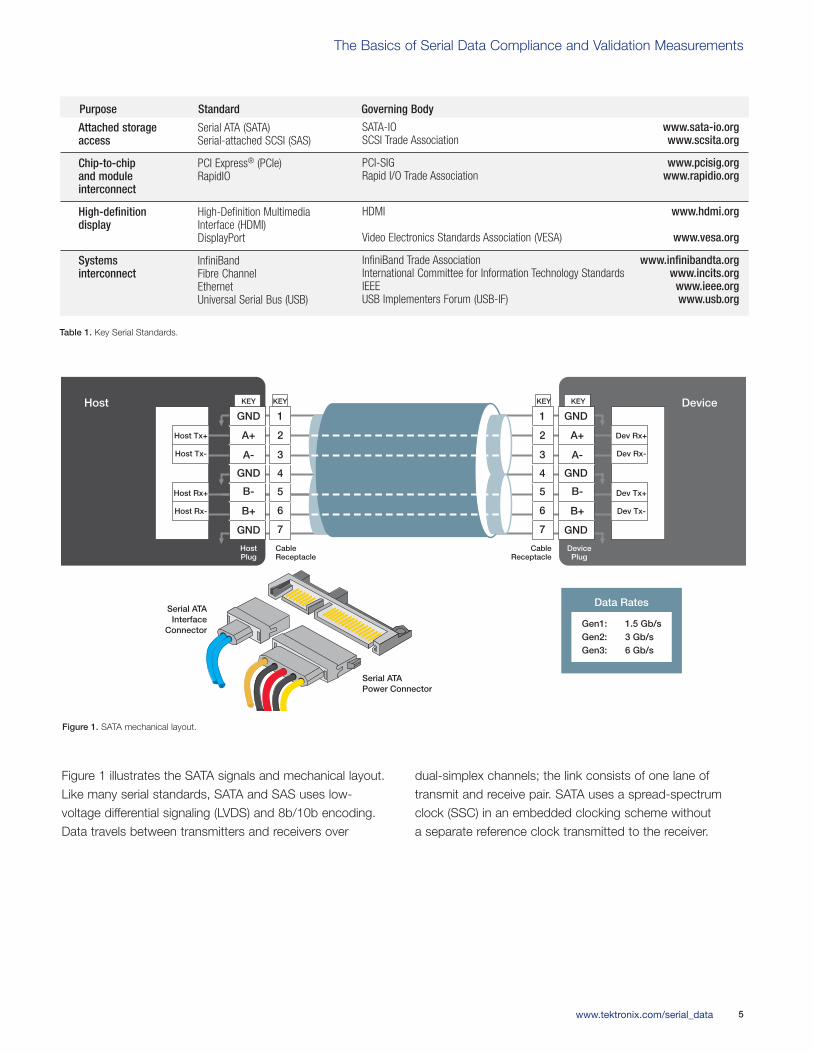
Figure 1. SATA mechanical layout.
Figure 1 illustrates the SATA signals and mechanical layout.Like many serial standards, SATA and SAS uses low-voltage differential signaling (LVDS) and 8b/10b encoding. Data travels between transmitters and receivers over
dual-simplex channels; the link consists of one lane oftransmit and receive pair. SATA uses a spread-spectrumclock (SSC) in an embedded clocking scheme without a separate reference clock transmitted to the receiver.
Table 1. Key Serial Standards.
Data Rates
Gen1: 1.5 Gb/sGen2: 3 Gb/sGen3: 6 Gb/s
Host DeviceKEY KEY KEY KEY
Host Tx+
Host Tx-
Host Rx+
Host Rx-
Dev Rx+
Dev Rx-
Dev Tx+
Dev Tx-
1GND
A+
B+
A-
B-
A+
B+
A-
B-
GND
GND
GND
GND
GND
2
3
4
5
6
7
1
2
3
4
5
6
7
Serial ATAInterface
Connector
Serial ATAPower Connector
HostPlug
Cable Receptacle
CableReceptacle
DevicePlug
The Basics of Serial Data Compliance and Validation Measurements
5www.tektronix.com/serial_data
Purpose Standard Governing Body
Attached storage Serial ATA (SATA)access Serial-attached SCSI (SAS)
Chip-to-chip PCI Express® (PCIe)and module RapidIOinterconnect
High-definition High-Definition Multimediadisplay Interface (HDMI)
DisplayPort
Systems InfiniBandinterconnect Fibre Channel
EthernetUniversal Serial Bus (USB)
SATA-IO www.sata-io.orgSCSI Trade Association www.scsita.org
PCI-SIG www.pcisig.orgRapid I/O Trade Association www.rapidio.org
HDMI www.hdmi.org
Video Electronics Standards Association (VESA) www.vesa.org
InfiniBand Trade Association www.infinibandta.orgInternational Committee for Information Technology Standards www.incits.orgIEEE www.ieee.orgUSB Implementers Forum (USB-IF) www.usb.org
6
PCI Express®
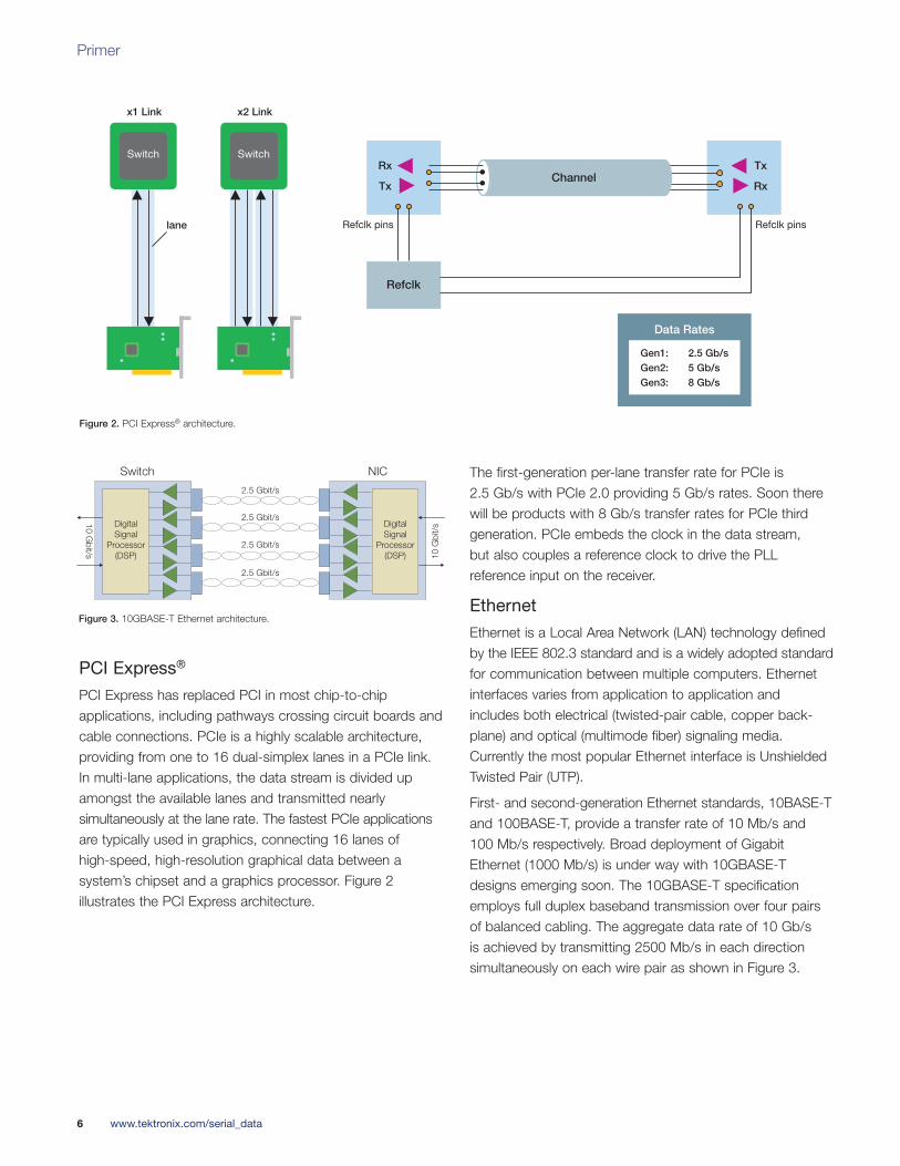
PCI Express has replaced PCI in most chip-to-chip applications, including pathways crossing circuit boards and cable connections. PCIe is a highly scalable architecture,providing from one to 16 dual-simplex lanes in a PCIe link.In multi-lane applications, the data stream is divided upamongst the available lanes and transmitted nearly simultaneously at the lane rate. The fastest PCIe applicationsare typically used in graphics, connecting 16 lanes of high-speed, high-resolution graphical data between a system’s chipset and a graphics processor. Figure 2 illustrates the PCI Express architecture.
The first-generation per-lane transfer rate for PCIe is 2.5 Gb/s with PCIe 2.0 providing 5 Gb/s rates. Soon therewill be products with 8 Gb/s transfer rates for PCIe thirdgeneration. PCIe embeds the clock in the data stream, but also couples a reference clock to drive the PLL reference input on the receiver.
Ethernet
Ethernet is a Local Area Network (LAN) technology definedby the IEEE 802.3 standard and is a widely adopted standardfor communication between multiple computers. Ethernetinterfaces varies from application to application andincludes both electrical (twisted-pair cable, copper back-plane) and optical (multimode fiber) signaling media.Currently the most popular Ethernet interface is UnshieldedTwisted Pair (UTP).
First- and second-generation Ethernet standards, 10BASE-Tand 100BASE-T, provide a transfer rate of 10 Mb/s and 100 Mb/s respectively. Broad deployment of GigabitEthernet (1000 Mb/s) is under way with 10GBASE-Tdesigns emerging soon. The 10GBASE-T specificationemploys full duplex baseband transmission over four pairsof balanced cabling. The aggregate data rate of 10 Gb/s is achieved by transmitting 2500 Mb/s in each directionsimultaneously on each wire pair as shown in Figure 3.
Tx
Rx
Data Rates
Gen1: 2.5 Gb/sGen2: 5 Gb/sGen3: 8 Gb/s
Channel
x1 Link
lane
Switch
x2 Link
SwitchRx
Tx
Refclk
Refclk pins Refclk pins
Figure 2. PCI Express® architecture.
Primer
6 www.tektronix.com/serial_data
Switch
DigitalSignal
Processor(DSP)
10 Gbit/s
NIC
DigitalSignal
Processor(DSP) 10
Gbi
t/s
2.5 Gbit/s
2.5 Gbit/s
2.5 Gbit/s
2.5 Gbit/s
Figure 3. 10GBASE-T Ethernet architecture.

USB
Universal Serial Bus has become known as the de factostandard for connecting personal computers and otherperipheral devices. USB 2.0 (480 Mb/s) was adopted in2000 with 40x speed improvement over the legacy USB 1.1(12 Mb/s) specification. Recently the USB 3.0 or SuperSpeedUSB specification was introduced at a 10x improvementover USB 2.0. With a 5 Gb/s data rate SuperSpeed USBwill accommodate data-intensive applications like HighDefinition video and fast I/O to flash memory devices.Because of the large adoption of legacy USB products USB3.0 provides complete backwards compatibility. Figure 5shows the link architecture for SuperSpeed USB.
HDMI/DisplayPort
The High Definition Multimedia Interface (HDMI) is the firstspecification designed specifically to address the needs ofthe consumer entertainment systems market. HDMI buildson the highly successful Digital Video Interface (DVI) for PCs and extends it with additional capabilities for homeentertainment devices, like large-screen, high-definition TVs and home theater systems. Figure 4 illustrates theHDMI architecture.
HDMI transmits high-resolution video and multi-channelaudio from a source to a sink. The specification definesthree data channels in the HDMI link with transmission rates from 250 Mb/s to 3.4 Gb/s, depending on the displayresolution.
While most high-speed serial standards rely on LVDS with8b/10b encoding, HDMI uses transition-minimized differentialsignaling, or TMDS, to reduce the number of transitions ona link and minimize electromagnetic interference (EMI).
HDMI also uses a reference clock transmitting at 1/10th thedata rate. A low-speed serial bus (I2C), called the DDC bus,exchanges configuration and identification data bi-directionallybetween the source and sink.
The DisplayPort specification defines a scalable digital display interface with optional audio- and content-protectioncapability for broad usage within business, enterprise, andconsumer applications. The interface is includes support fortwo data rates: Reduced Bit Rate (1.62 Gb/s) and High BitRate (2.7 Gb/s).
HDMI Source HDMI Sink
Transmitter Receiver
CEC Line
Display Data Channel (DDC)
VideoTMDS Channel 0
TMDS Channel 1
TMDS Channel 2
TMDS Clock Channel
Video
Audio Audio
EDIDROM
Data Rates
250 Mb/s to 3.4 Gb/s
Figure 4. HDMI architecture.
The Basics of Serial Data Compliance and Validation Measurements
7www.tektronix.com/serial_data
Figure 5. USB Architecture.

Primer
8 www.tektronix.com/serial_data
Common Architectural Elements
All the high-speed serial standards follow a layered model,as illustrated in Figure 6. The Physical layer comprises anelectrical and logical sub-block. This primer focuses on the electrical sub-block, where electrical compliance testingis completed.
Many high-speed serial standards incorporate the same orsimilar architecture elements at the electrical level, such as:
Differential signaling (LVDS or TMDS) for high data rates and high noise immunity
8b/10b encoding to improve signal integrity and reduce EMI
Embedded clocks and some with reference clocks
Spread-spectrum clocking to reduce EMI
Equalization to compensate for signal attenuation fromlossy channels
Typical measurements include jitter, amplitude, differentialskew, risetime/falltime, and common mode
Specifications and testing requirements evolve as moreinsight is gained and the standards advance
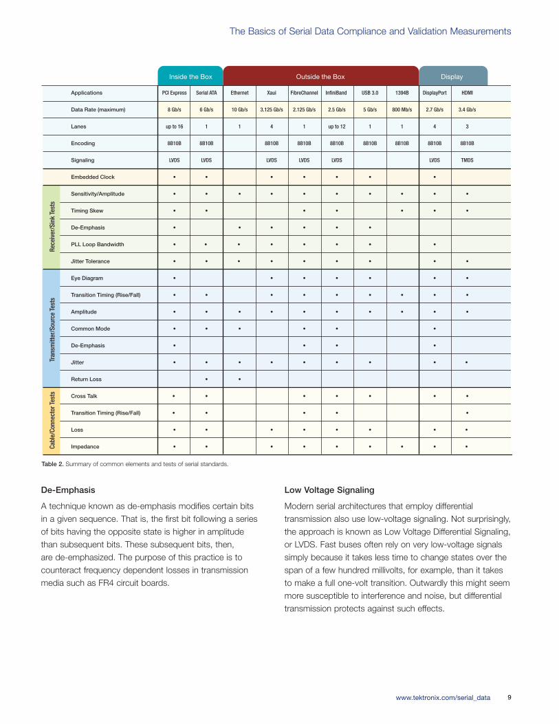
Table 2 lists some of the architectures’ key elements andcompliance tests.
Differential Transmission
Differential transmission has been a part of communicationstechnology since the early days of telephone networks. Adifferentially-transmitted signal consists of two equal andopposite versions of the waveform traveling down twoconductors to a differential receiver1. When the signal onone leg of the differential path is going positive, the signalon the other leg is going equally negative, as shown inFigure 2. These two mirror images of the signal combine atthe destination. Differential techniques resist crosstalk,externally induced noise, and other degradations. Properlydesigned and terminated, a differential architecture providesa robust path for sensitive high-frequency signals.
8b/10b Signal Encoding
Many serial standards employ 8B/10B encoding, an IBMpatented technology used to convert 8-bit data bytes into10-bit Transmission Characters. These TransmissionCharacters improve the physical signal to bring about severalkey benefits: bit synchronization is more easily achieved;the design of receivers and transmitters is simplified; errordetection is improved; and control characters (such as theSpecial Character) can be more readily distinguished fromdata characters.
Embedded Clocks
Many (if not most) current serial devices rely on embeddedclock signals to maintain synchronization between transmittingand receiving elements. There is no separate clock signalline; instead, the timing information resides in the data signal.As we will see later in this document, this imposes certainrequirements on the data signal. Encoding methods such as8b/10b are used to guarantee that usable reference edgesoccur regularly enough to provide the needed synchronization.
Digital Validationand Debug
Analog Validationand Compliance
Data Link
Transaction
Physical
Logical Sub-block
Electrical Sub-block
Data Link
Transaction
Physical
Logical Sub-block
Electrical Sub-block
Rx TxTx Rx
Figure 6. Layered model.
De-Emphasis
A technique known as de-emphasis modifies certain bits in a given sequence. That is, the first bit following a series of bits having the opposite state is higher in amplitude than subsequent bits. These subsequent bits, then, are de-emphasized. The purpose of this practice is to counteract frequency dependent losses in transmissionmedia such as FR4 circuit boards.
Low Voltage Signaling
Modern serial architectures that employ differential transmission also use low-voltage signaling. Not surprisingly,the approach is known as Low Voltage Differential Signaling,or LVDS. Fast buses often rely on very low-voltage signalssimply because it takes less time to change states over thespan of a few hundred millivolts, for example, than it takesto make a full one-volt transition. Outwardly this might seemmore susceptible to interference and noise, but differentialtransmission protects against such effects.
Table 2. Summary of common elements and tests of serial standards.
The Basics of Serial Data Compliance and Validation Measurements
9www.tektronix.com/serial_data
Applications PCI Express Serial ATA Ethernet Xaui FibreChannel InfiniBand USB 3.0 1394B DisplayPort HDMI
Data Rate (maximum) 8 Gb/s 6 Gb/s 10 Gb/s 3.125 Gb/s 2.125 Gb/s 2.5 Gb/s 5 Gb/s 800 Mb/s 2.7 Gb/s 3.4 Gb/s
Lanes up to 16 1 1 4 1 up to 12 1 1 4 3
Encoding 8B10B 8B10B 8B10B 8B10B 8B10B 8B10B 8B10B 8B10B 8B10B
Signaling LVDS LVDS LVDS LVDS LVDS LVDS TMDS
Embedded Clock • • • • • • •
Sensitivity/Amplitude • • • • • • • • • •
Timing Skew • • • • • • •
De-Emphasis • • • • • •
PLL Loop Bandwidth • • • • • • • •
Jitter Tolerance • • • • • • • • •
Eye Diagram • • • • • • •
Transition Timing (Rise/Fall) • • • • • • • • •
Amplitude • • • • • • • • • •
Common Mode • • • • • •
De-Emphasis • • • •
Jitter • • • • • • • • •
Return Loss • •
Cross Talk • • • • • • •
Transition Timing (Rise/Fall) • • • • •
Loss • • • • • • • •
Impedance • • • • • • • • •
Inside the Box DisplayOutside the Box
Cabl
e/Co
nnec
tor T
ests
Tr
ansm
itter
/Sou
rce
Test
s Re
ceiv
er/S
ink
Test
s
Primer
10 www.tektronix.com/serial_data
Next-generation Serial ChallengesAt the data rates next-generation serial standards operate,analog anomalies of the signal have a greater impact onsignal integrity and quality than ever before. Conductors in signal pathways, including circuit board traces, vias, connectors, and cabling, exhibit greater transmission lineeffects with return losses and reflections that degrade signal levels, induce skewing, and add noise.
Gigabit Speeds
With each increase in transfer rates of the standards, the UI shrinks, and the tolerances in transmitter signal qualityand receiver sensitivity become tighter. Low-voltage differ-ential signals and multi-level signaling are more vulnerableto signal integrity issues, differential skew, noise, and inter-symbol interference (ISI) as speeds increase. There is greater susceptibility to timing problems, impedance discontinuities between a transmitter and receiver, and system level interaction between hardware and software.Multi-lane architectures amplify design complexity andpotential for lane skew timing violations and crosstalk.
Jitter
Today’s higher data rates and embedded clocks meangreater susceptibility to jitter, degrading bit error rate (BER) performance. Jitter typically comes from crosstalk,system noise, simultaneous switching outputs, and otherregularly occurring interference signals. With faster rates,multi-lane architectures, and more compact designs, there are more opportunities for all these events to affectdata transmission in the form of signal jitter.
Transmission Line Effects
The signal transmitter, conductor pathways, and receiverconstitute a serial data network. Buried in that network are distributed capacitance, inductance, and resistance that have diverse effects on signal propagation as frequencies increase. Transmission line effects rise from this distributed network and can significantly impact signal quality and lead to data errors.
Noise
Noise is unwanted aberrations in the amplitude domain that appear in the signal. Noise comes from both externalsources, such as the AC power line, and internal sources,including digital clocks, microprocessors, and switched-mode power supplies. Noise can be transient or broadbandrandom noise and can lead to phase errors and signalintegrity problems. Like jitter in the frequency domain, with faster signaling, noise in the amplitude domain adds variations that can have a critical impact on BER performance.
Compliance TestingSerial standards normally include amplitude, timing, jitter,and eye measurements within their compliance testingspecifications. The latest versions of some standards add focus, compared to previous versions, on SSC clocking, receiver sensitivity testing, and measurement of return loss and reflections on connectors, cables, and other pathways. Not all measurements are required for compliance with every standard.
Test points are specified in the standard’s compliance test document or the specification itself.

The Basics of Serial Data Compliance and Validation Measurements
11www.tektronix.com/serial_data
Eye Measurements
Key compliance verification comes from eye measurements.An eye diagram is shown in Figure 7. Eye measurementsresult from superimposing multiple, one unit interval (UI) signal captures (the equivalent of one clock cycle) of thedata stream, triggered to the recovered clock. Failure zones in the middle of the eye and above and below theeye are typically indicated by a “mask” (blue areas), showing the boundaries the test must not violate. Eyemeasurements are further discussed in the Analysis section later in this document.
The following tables encapsulate some of the key measurements commonly required at plug-fests (to provecompliance and interoperability) and ultimately, in certifiedcompliance verification procedures.
Amplitude Tests
The amplitude tests listed in Table 3 verify that the signalachieves the voltage levels and stability to reliably propagatethrough the transmission media and communicate a proper“one” or “zero” to the receiver.
Figure 7. Eye diagram on an oscilloscope.
Table 3. Overview of Amplitude Tests.
Test Overview
Differential Voltage
Eye Height
De-Emphasis
Common ModeVoltage (AC, DC)
Every specification defines peak-to-peakdifferential voltage. This is the fundamentalspecification to guarantee that the transmitter is generating the correct voltage levels.
Eye height is the eye opening in the ampli-tude domain; it represents the amplitude at the sample point of the receiver circuit.Eye height is measured at the .5 UI point,as referenced to the recovered clock. Eyediagrams are covered in more detail in thesection on Analysis later in this document.
During signal propagation, the transmis-sion media can roll off and/or slow downthe slew of a bit transitioning low to highor high to low. To compensate for thiseffect, the transmitter generates transitionbits with slightly higher amplitude than fol-low-on bits of the same value. By makingthe transition bit higher in amplitude thanthe subsequent bits, the signal arrives atthe receiver pins with an “open eye.”
De-emphasis is the ratio of amplitudesbetween the second and subsequent bitsfollowing a transition bit and the transition bit(Figure 8). Other terms for de-emphasis arepre-emphasis and transmitter equalization.
Common mode imbalance and noise onthe transmitter can create undesirableeffects in the differential signal. It is oftenuseful to break apart the differential signalinto its single-ended components to troubleshoot such issues. This techniquealso pinpoints crosstalk and noise effectsthat may be coupling into one side of thedifferential pair and not the other.

Primer
12 www.tektronix.com/serial_data
Timing Tests
The timing tests listed in Table 4 verify the signal is free from excess timing variations and its transitions are fastenough to preserve the critical data values the signal ismeant to deliver. These tests, which require uncompro-mised performance on the part of the measurement toolset,detect aberrations and signal degradation that arise fromdistributed capacitance, resistance, crosstalk, and more.
Jitter Tests
With faster data rates, jitter becomes one of the most difficult issues to resolve, which is one reason jitter meas-urements continue to be a topic of extensive discussion in standards bodies’ working groups. It is also a focus of companies that develop specialized analysis tools to help you quickly identify the causes and results of jitterand to understand this complex issue.
Jitter is a result of spectral components, both deterministicand random. To guarantee interoperability, the transmittermust not develop too much jitter, and the receiver must beable to tolerate a defined amount of jitter and still recoverthe clock and de-serialize the data stream. Other signal characteristics, such as amplitude and rise time can affectany jitter tolerance property. In effect, jitter is a bit error ratio measurement and is usually quantified in terms of totaljitter at a specified bit error ratio (BER).
Time (UI)
Vo
lta
ge
De-emphasis Amplitude
Figure 8. De-emphasis on a data stream.
Table 4. Overview of Timing Tests
Test Overview
Unit Interval (UI)and Bit Rate
Rise/Fall Time
Eye Width
Variations in the embedded clock frequency canbe measured by looking at the mean measure-ment of the embedded clock over a large numberof consecutive cycles, as many as 1 million ormore. In some standards, if the mean measure-ment is more than 100 parts per million (PPM)away from the specified value, the DUT fails.
Risetimes that are too fast can cause EMI issues,while those that are too slow can cause data errors.
Some standards have not included rise time aspart of the compliance test series simply becauseof the risetime measurement errors introduced bythe probe/instrument combination. However, byapplying the “square root of the sum of thesquares” formula to the measured value, it is possible to determine whether the transmit driveris approaching a rise/fall time failure. In addition,recent oscilloscope tools use special filteringtechniques to de-embed the measurement system’s effects on the signal, displaying edge times and other signal characteristics as they are presented at the probe tip.
Eye width offers a qualitative measurement of signal timing and jitter. Like eye height,it is bounded by the mask, and any violations of the mask in the time domain indicate failure of compliance.
Not all standards accept the eye diagram as a final determination of jitter compliance. Forexample, Section 6 of the Serial ATA specificationsays that the statistical certainty achieved by capturing a waveform and comparing it to a maskcannot guarantee compliance to the required 10-12 BER. The eye diagram measurements donot capture enough edges.
Time interval error (TIE) is the basis for many jitter measure-ments. TIE is the difference between the recovered clockedge (the jitter timing reference) and the actual waveformedge. Performing histogram and spectrum analysis on a TIE waveform provides the basis for advanced jitter meas-urements. Histograms also help you isolate jitter induced by other circuits, such as switching power supplies.
Jitter measurements generally require long test times, sincethey must record literally trillions of cycles to ensure anaccurate representation at 10-12 BER performance. An oscilloscope with high capture rate and jitter analysis tools can reduce test times for these jitter tolerance tests.
See the Analysis section later for more details about jitter measurements.
Receiver Sensitivity Tests
The governing bodies of some standards have focusedmore on receiver sensitivity testing in their latest test specifications. Receiver sensitivity verifies the ability of theclock-data recovery (CDR) unit and de-serializer in thereceiver component to accurately recover the clock and thedata stream under certain adverse signal characteristics,including jitter, amplitude, and timing variations. This area of testing is covered in more detail in Receiver SensitivityTesting below.
Circuit Board and Interconnect Tests
The transmission media play an increasingly critical role in signal quality. An LVDS signal running at multi-gigabitdata rates through a low-cost medium, such as FR4, plus connectors and cables, poses many layout challenges in both product and test fixture design and testing. Many standards require a more critical look at characterizing media with loss, impedance, crosstalk testing, and eye analysis.
Compliance Testing SolutionsGetting the right signal with minimal impact from the measurement system is paramount in evaluating performance of a new design. Five areas are critical to the testing process:
Connectivity
Pattern Generation
Receiver Testing
Acquisition
Analysis
Connectivity
Measurement pathways, including the DUT-to-oscilloscopepath, have transmission line effects and can lead to degraded signals and test failure. Proper connectivity withthe correct probe is essential.
The mechanical portion of the standard, sometimes called the physical media dependent (PMD) specification, often determines how to connect to the DUT. With many standards, you will find diverse configurations, each with its own unique characteristics.
There are five approaches to the probing challenge:
TriMode™ differential probes enable single-ended and differential measurements from a single setup on a test point
Pseudo-differentially connected movable probes for single-ended, differential, and common-mode measurements
SMA pseudo-differentially connected probes for connecting to fixtures
True differential movable probes for direct, differential measurements
SMA true differential probes for connecting to fixtures
The Basics of Serial Data Compliance and Validation Measurements
13www.tektronix.com/serial_data

Primer
14 www.tektronix.com/serial_data
It is important to note that any probe will impose someloading on the Device Under Test (DUT). Every probe has its own circuit model whose impedance can change withincreasing frequency. This can affect the behavior of theobserved circuit and influence the measurement, factorsthat must be considered when evaluating results.
TriMode™ Differential Probes
TriMode probes change differential probing by enabling single-ended, differential, and common mode measurementswith a single connection to the DUT.
Traditional measurement methods require two single-endedprobes for common mode measurements, plus a differentialprobe setup for true differential signal acquisition (Figure9a). TriMode probes accomplish both setups with a singleprobe (Figure 9b).
Pseudo-differentially Connected Movable Probes
Troubleshooting work may require probing circuit pointsanywhere on a device’s circuit board. This makes it necessary to probe individual circuit traces and pins withmovable probes. Two single-ended active probes, one on each side of the differential signal, can be used for pseudo-differential measurements and common-modemeasurements. Figure 10 illustrates this type of connectivity.
Two channels of the oscilloscope capture two channels of data, which are subsequently processed as one signal,resulting in a math waveform. Because the two sides of the waveform enter two separate oscilloscope input channels, the inputs must be deskewed before making any measurements to eliminate instrument impacts on the acquisition.
Figure 9a. Traditional differential probing. Figure 9b. Tri-Mode simplifies probing.

SMA Pseudo-differentially Connected Probes
Many compliance test fixtures and prototype circuits are fitted with SMA high-frequency connectors for external test instrumentation. Under these conditions, the SMApseudo-differential approach is a practical solution. Here the output of the transmitter connects directly to two inputs of the oscilloscope, each with an input impedance of 50Ω. SMA adapters provide the necessary mechanicaltermination on the front panel of the oscilloscopes.
As explained earlier, this pseudo-differential technique consumes two channels of the oscilloscope, and probedeskewing is critical. Figure 11 illustrates this kind of fixture connectivity.
True Differential Movable Probes
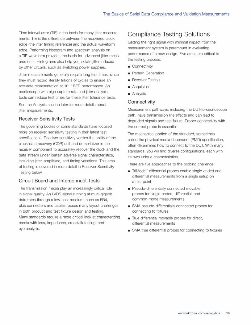
A true differential active probe is optimized as a low-loss,high-fidelity path for differential signals. Figure 12 showssuch a probe capturing the receive side of a connector-based card-to-card serial link.
Unlike the pseudo-differential connection, this proberequires only one oscilloscope channel and makes the subsequent math steps unnecessary. This offers, amongother advantages, the ability to use several channels of the oscilloscope to simultaneously capture multiple lanes at the highest sample rates. It is also useful for debuggingmultiple high-speed test points.
SMA True Differential Probes
The SMA input differential probe is also ideal for compliancetests where interoperability points are defined at the card-to-card or card-to-cable interface. A 100Ω matchedtermination network properly terminates both legs of the differential signal to any user-provided common mode voltage. The voltage may be at ground potential or a termination voltage appropriate to the logic family beingtested. The common mode connector can also be left open if the transmitter will drive a 100Ω differential load.Figure 13 illustrates a true differential SMA probe attachedto a card-to-card interface and fixture.
ECB connector ECB
termination inside device
CH1CH2
Serdes
P7380AP7380A
VDIFF = (CH1 - CH2)
Serdes
Tx Rx
Figure 10. Pseudo-differential probing of a receiver input.
ECB
SMA Adaptors
SMA Connectors
50 Ω SMA Cables
Test Fixture
Connector
CH1CH2
Serdes
Tx
50 Ω Termination
}
Figure 11. Pseudo-differential connecion to a fixture using SMA-terminated cables.
The Basics of Serial Data Compliance and Validation Measurements
15www.tektronix.com/serial_data
Primer
16 www.tektronix.com/serial_data
Fixtures
Like all other aspects of serial architectures, increased datarates can have a significant impact on test fixtures. Youmust qualify any existing fixtures under the new standardsto ensure they continue to deliver a correct signal to themeasurement system. With the faster rates for PCI Expressand SATA, the impact on existing fixtures is notable, andrequires redesign and new board layouts.
In some cases, low cost media, such as FR4, are no longersuitable for new designs based on second- and third-gen-eration serial architectures. These media present too manylosses and returns to adequately propagate a signal andmaintain proper signal integrity. You might need to evaluatenewer, more expensive materials. In some cases you mayneed to incorporate additional equalization techniques suchas receiver equalization to overcome signal loss.
Pattern Generation
Each standard’s test document specifies the “golden” pattern that must be applied to the DUT for complianceverification. This specified pattern is critical to achieve the desired results.
In some cases, like PCI Express, the transmitter/receivergenerates its own test sequence. Other standards requiremore complex handling of the signal, possibly with helpfrom a host processor.
When an external signal is required, the test equipmentmust generate the golden pattern at the right frequency and with all the necessary characteristics to adequately test the device according to the test specification. The righttool for this is the programmable signal source, including:
Data timing generators that offer standard test signals, such as TS1 and TS2 training signals andPseudo-random bit streams (PRBS)
Arbitrary waveform generators that provide highly definable real-world signals along with digital patterns
Jitter sources that vary input signals for stress testing
New all-in-one signal generators that simplify testing withanalog waveforms, digital patterns, and signal sources to vary outputs with diverse modulation schemes
ECB connector ECB
CH1CH2
Serdes
P73xx
VDIFF - CH1
Serdes
Tx Rx
Figure 12. True differential probing of a receiver input.
ECB Test Fixture
Connector
P7380SMA
CH1CH2
Serdes
Tx
Oscilloscope ground connection
Phase-matched SMA cables
50 Ω
50 Ω
VDIFF - CH1
+
+
+
-
-
-
Figure 13. Differential connection on a fixture using SMA-terminated cables.
To automate the testing process, connectivity betweenother test instruments, such as oscilloscopes, logic analyz-ers, and PCs, helps accelerate compliance verification.Programmability using math waveforms generated fromapplications like Matlab, and the ability to capture and re-generate waveforms can also speed testing.
Receiver Sensitivity Testing
The receiver is at the end of a possibly diverse transmissionpath. Yet, it must interoperate with the many different transmitters connected through various interconnects, each with its own effect on the signal.
In order to guarantee interoperability, the receiver section, particularly the clock-data recovery (CDR) unit and de-serializer, must operate correctly under a broadrange of conditions. The CDR must extract the clock in thepresence of variations in jitter and amplitude. Similarly, thede-serializer must tolerate a specified amount of amplitude,jitter, and skew to comply with a particular standard.
The Test Process
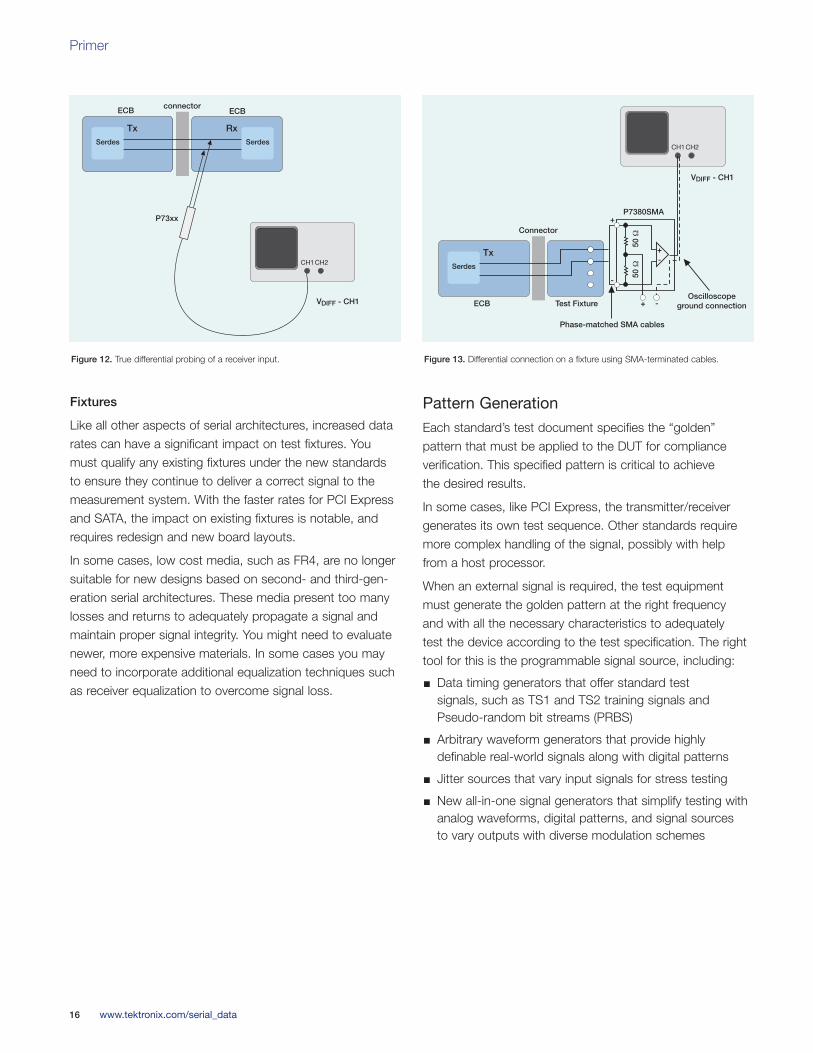
Figure 14 illustrates a single-lane SATA receiver test setup.While the exact test parameters, procedures, and tolerances vary among standards, the basic test methodology comprises the following:
Set the device to loopback mode and monitor thetransmitter output with a logic analyzer and/or oscilloscope, serial bus analyzer, or error detector tocheck that the transmitted pattern is the same as thetest pattern
Insert the specified golden test pattern
Vary the amplitude to make sure the receiver can accurately recognize 0 and 1 values
Vary the skew between differential pairs to allow for tolerances in board layout and cabling
Insert jitter to make sure the CDR phase-locked loop(PLL) can track the input
Figure 14. SATA receiver testing setup.
AWG7122B
Arbitrary Waveform Generator
Training Sequence
Oscilloscope and
Logic Analyzer
Serial ATA
Change amplitude, slopes and crossings. Add jitter and noise.
The Basics of Serial Data Compliance and Validation Measurements
17www.tektronix.com/serial_data
Primer
18 www.tektronix.com/serial_data
Seeing Inside the Receiver
The difficulty with receiver testing and debugging is that you cannot directly probe the signal within the device todebug problems. Many receivers are designed with input filters that compensate for transmission line losses andeffects, delivering a “clean” signal to the CDR. So, an oscilloscope probe at a receiver’s input pins sees the signals before the filter is applied.
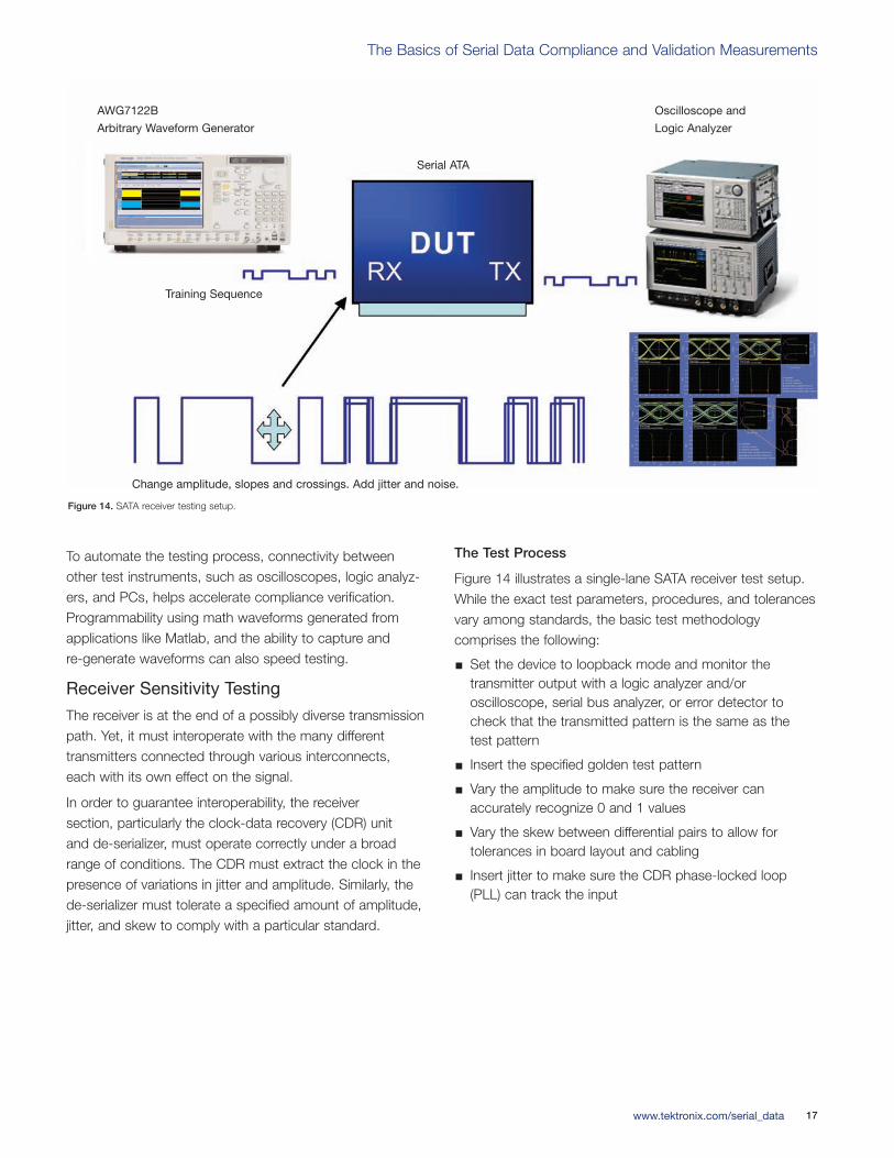
Advanced oscilloscopes with programmable DSP filteringtechniques enable you to acquire signals at “virtual testpoints” within the receiver to view signal characteristics after filtering. By applying the input filter coefficients to theoscilloscope’s Math system, the oscilloscope displays the signal characteristics beyond the input filter and anyequalization that may be applied. This reveals more accurate eye testing at the CDR input where clock recoveryand equalization are accomplished and jitter has its impact.Note in Figures 15a and 15b the difference in results of eyemeasurements due to FIR filtering.
Receiver Amplitude Sensitivity Measurements
Signal losses are inevitable before reaching the receiver.Amplitude sensitivity measurements check that the receiver can accurately recognize the proper bit value once the signal reaches the CDR and de-serializer.
Receiver Timing Measurements
Timing tests vary the skew of the differential pair and edge rates to verify the receiver’s tolerance of changes insignal timing. Differential outputs on the pattern generatoror arbitrary waveform generator providing the test signalsare essential.
Figure 15a. USB 3.0 signal at the receiver (blue) and after equalization (yellow). Figure 15b. USB 3.0 eye before equalization (left) and after equalization (right).
Receiver Jitter Tolerance Measurements
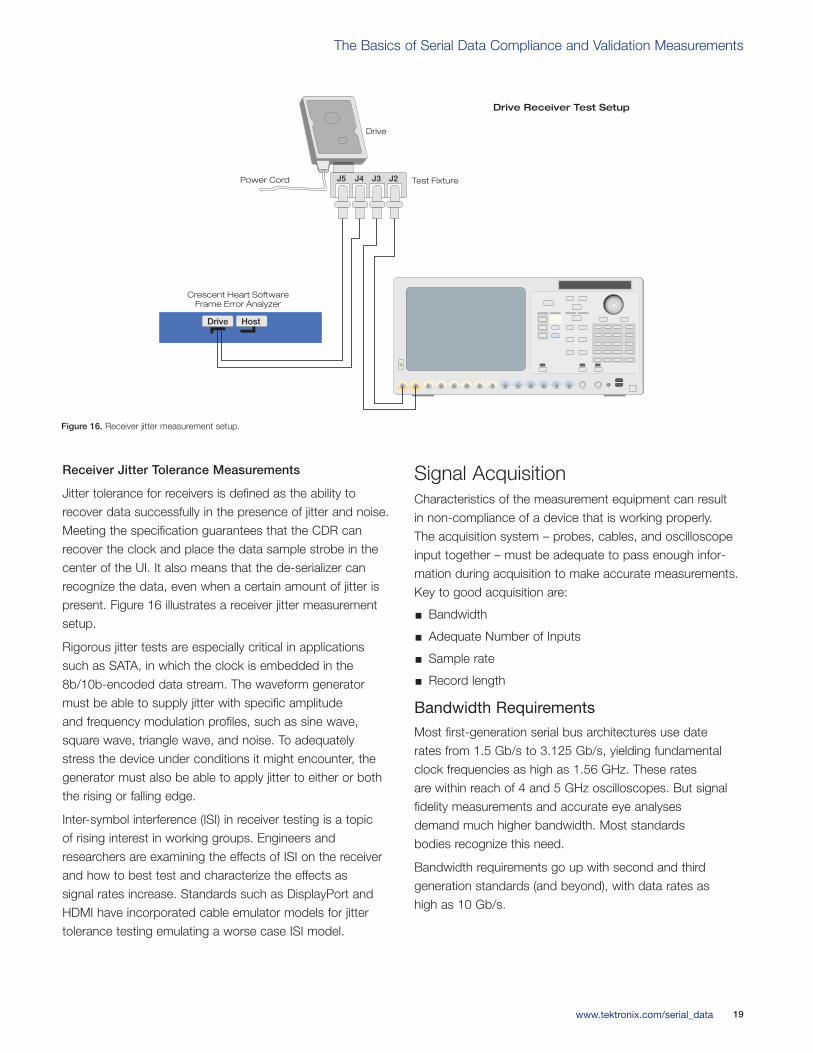
Jitter tolerance for receivers is defined as the ability torecover data successfully in the presence of jitter and noise.Meeting the specification guarantees that the CDR canrecover the clock and place the data sample strobe in thecenter of the UI. It also means that the de-serializer can recognize the data, even when a certain amount of jitter ispresent. Figure 16 illustrates a receiver jitter measurementsetup.
Rigorous jitter tests are especially critical in applicationssuch as SATA, in which the clock is embedded in the8b/10b-encoded data stream. The waveform generatormust be able to supply jitter with specific amplitude and frequency modulation profiles, such as sine wave,square wave, triangle wave, and noise. To adequately stress the device under conditions it might encounter, thegenerator must also be able to apply jitter to either or boththe rising or falling edge.
Inter-symbol interference (ISI) in receiver testing is a topic of rising interest in working groups. Engineers andresearchers are examining the effects of ISI on the receiver and how to best test and characterize the effects as signal rates increase. Standards such as DisplayPort andHDMI have incorporated cable emulator models for jitter tolerance testing emulating a worse case ISI model.
Signal AcquisitionCharacteristics of the measurement equipment can result in non-compliance of a device that is working properly. The acquisition system – probes, cables, and oscilloscopeinput together – must be adequate to pass enough infor-mation during acquisition to make accurate measurements.Key to good acquisition are:
Bandwidth
Adequate Number of Inputs
Sample rate
Record length
Bandwidth Requirements
Most first-generation serial bus architectures use date rates from 1.5 Gb/s to 3.125 Gb/s, yielding fundamentalclock frequencies as high as 1.56 GHz. These rates are within reach of 4 and 5 GHz oscilloscopes. But signalfidelity measurements and accurate eye analyses demand much higher bandwidth. Most standards bodies recognize this need.
Bandwidth requirements go up with second and third generation standards (and beyond), with data rates as high as 10 Gb/s.
Drive Receiver Test Setup
Crescent Heart Software Frame Error Analyzer
Test Fixture
Drive
Power Cord
Drive
J5 J4 J3 J2
Host
Figure 16. Receiver jitter measurement setup.
The Basics of Serial Data Compliance and Validation Measurements
19www.tektronix.com/serial_data

Bandwidth and Transitions
Often, the rise-time requirements for a standard are moredemanding on bandwidth than the data rates. Table 5 listsbandwidth requirements needed for various risetime measurement accuracies at risetimes found in today’s standards.
Both the oscilloscope’s and probe’s transition times affect the signal’s measured risetimes and falltimes. The equation below shows the relationship between the probe/oscilloscope system, signal, and displayed risetime measurements. The probe and oscilloscope mustbe considered as a system and removed from the displayedmeasurement to arrive at the signal’s true risetime.
For example, a system with a 20% to 80% risetime specification of 65 ps, when applied to a signal with a truerisetime of 75 ps would display a measurement of 99 ps.This is an unavoidable measurement artifact of the system.Thus, it is desirable to minimize the impact of the measure-ment system whenever possible with a faster risetime specification for both the oscilloscope and probe.
Acquiring From Multiple Lanes
High data rates, low-cost media, and multiple lane designswith standards like HDMI can have adverse effects on inter-lane skew and crosstalk. An oscilloscope providingsimultaneous real-time data capture across multiple lanes,with the performance necessary to service the latest generation of serial standards can speed and simplify testing, validation, and debugging.
With time-correlated, captured waveform data on multiplelanes you gain a better understanding of the context inwhich an error occurred. With HDMI, recording all lanes of time-correlated data provides insight into, not only theoffending event, but also the events that preceded and followed it on every lane.
tr(displayed) = tr(system)2 + tr(signal)2
Primer
20 www.tektronix.com/serial_data
Table 5. Bandwidth and Risetime Measurement Accuracy.
Signal AccuracyRise/Fall Time 3% 5%a 10%b
100 ps 5.6 GHz 4.8 GHz 4.0 GHz
75 ps 7.5 GHz 6.4 GHz 5.3 GHz
60 ps 9.3 GHz 8.0 GHz 6.7 GHz
50 ps 11.2 GHz 9.6 GHz 8.0 GHz
40 ps 14.0 GHz 12.0 GHz 10.0 GHz
30 ps 18.7 GHz 16.0 GHz 13.3 GHz
aRequired BW = Frequency X 1.2
bFrequency = 0.4/ Rise-time (20% to 80%)
The Basics of Serial Data Compliance and Validation Measurements
21www.tektronix.com/serial_data
Sample Rate and Record Length
Along with adequate bandwidth to capture signal character-istics, an oscilloscope must store enough waveform infor-mation (record length) with enough detail (sample rate) atthe required bandwidth to complete the standardized tests.Each standard specifies the minimal amount of data to capture to complete a test. Of course, more data withgreater detail affords deeper analysis into signal anomaliesthat might occur over longer time periods. Advanced oscilloscopes, with longer record lengths, faster samplingrates, and wider bandwidth, can use these features to their advantage and your benefit, to present a higher degreeof analysis.
Advanced oscilloscopes with long record lengths and built-in analysis tools can include proprietary analysis techniquesthat reveal greater detail about the signal over the entireacquisition, offering more confidence in the design. Forexample, while PCIe 1.0 requires a minimum sampling of 250 cycles for compliance verification, with a capture of 1 million cycles, advanced tools allow analysis of anycontiguous 250 cycles throughout the record length to evaluate signal quality in more depth.
For multi-lane signal acquisition, record length and samplerate should apply across each lane in a multi-channel oscilloscope to ensure the greatest detail possible during acquisition.
Signal AnalysisThe correct application of the right probes, the golden pattern applied to the DUT, and the best choice in the testinstrument’s acquisition system, help with a higher degree ofconfidence in the output of your analysis.
Automated measurement and analysis tools are commonlyused to speed the selection and application of compliancetests. Oscilloscopes with automated analysis tools helpaccelerate and evaluate BER, eye opening, return loss, and reflection measurements. Advanced instruments offernew, unique approaches and techniques to perform deeperanalysis and troubleshooting for greater confidence in designoutcomes and faster isolation of problems.
Real-time or Equivalent-time Oscilloscopes
While most standards design their tests around real-timesampling oscilloscopes, and these scopes are most oftenused in compliance verification, other standards requireequivalent-time (also called sampling) oscilloscopes. Eachtype has its own unique requirements and advantages.
Real-time (RT) oscilloscopes acquire an extended set ofmeasurement data from a single trigger, and then performmeasurement and analysis on the data. The amount anddetail of data are limited by the oscilloscope’s bandwidth,record length, and sample rate. Advanced instruments use software digital signal processing (DSP) to recover the clock, which means different clock recovery models can be quickly loaded to adapt to different tests. The real-time oscilloscope can acquire data from any type ofinput stimulus, whether it’s a fixed, repeating pattern or a single anomaly.
Primer
22 www.tektronix.com/serial_data
Equivalent-time (ET/sampling) oscilloscopes build up awaveform from samples of a repeating signal. These oscilloscopes can sample and “create” much faster signalsthan real-time oscilloscopes, but they require a repeatingsignal. The fastest oscilloscopes are typically ET systems.Sampling oscilloscopes rely on a hardware-based clockrecovery unit that must trigger the system for every sample. It typically takes a much longer time to performmeasurements, requiring many repeated acquisitions, butan advanced triggering system that speeds re-arm time for the trigger circuit helps shorten measurement times.
Modern, advanced sampling oscilloscopes also integratetime domain reflectometry (TDR) and time domain transmission(TDT) capabilities, and offer S-parameter-based modelingand analysis of circuits and transmission media. These features enable de-embedding of test equipment effectsand circuit elements, plus advanced signal processing, toreveal more accurate signal characteristics and providegreater insight to causes of design challenges.
Eye Analysis
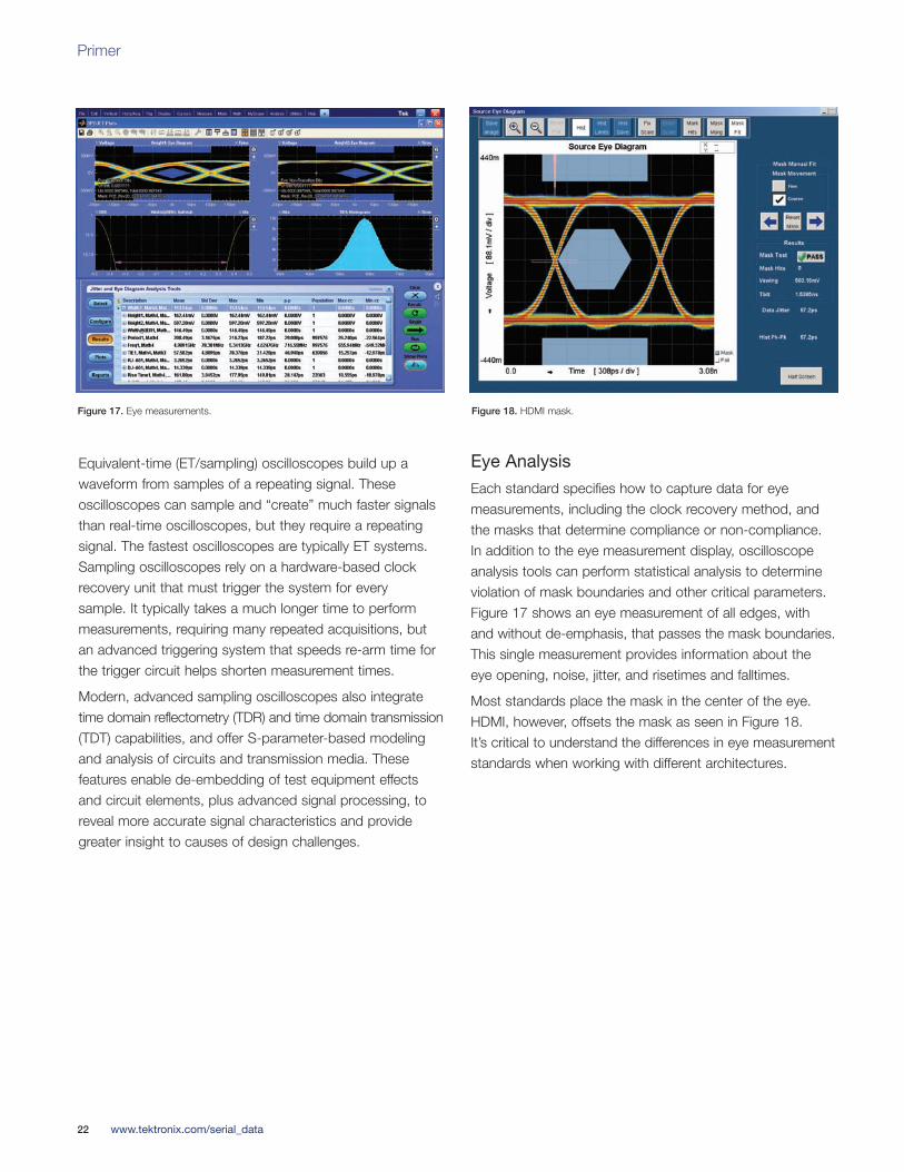
Each standard specifies how to capture data for eye measurements, including the clock recovery method, andthe masks that determine compliance or non-compliance.In addition to the eye measurement display, oscilloscopeanalysis tools can perform statistical analysis to determineviolation of mask boundaries and other critical parameters.Figure 17 shows an eye measurement of all edges, withand without de-emphasis, that passes the mask boundaries.This single measurement provides information about theeye opening, noise, jitter, and risetimes and falltimes.
Most standards place the mask in the center of the eye.HDMI, however, offsets the mask as seen in Figure 18. It’s critical to understand the differences in eye measurementstandards when working with different architectures.
Figure 17. Eye measurements. Figure 18. HDMI mask.
The Basics of Serial Data Compliance and Validation Measurements
23www.tektronix.com/serial_data
Jitter Analysis
Jitter measures the difference between an expected signaledge, based on a golden clock model specified by eachstandard, and the actual edge recovered from the embed-ded clock. Too much jitter degrades BER performance.
Determining Jitter and BER Performance
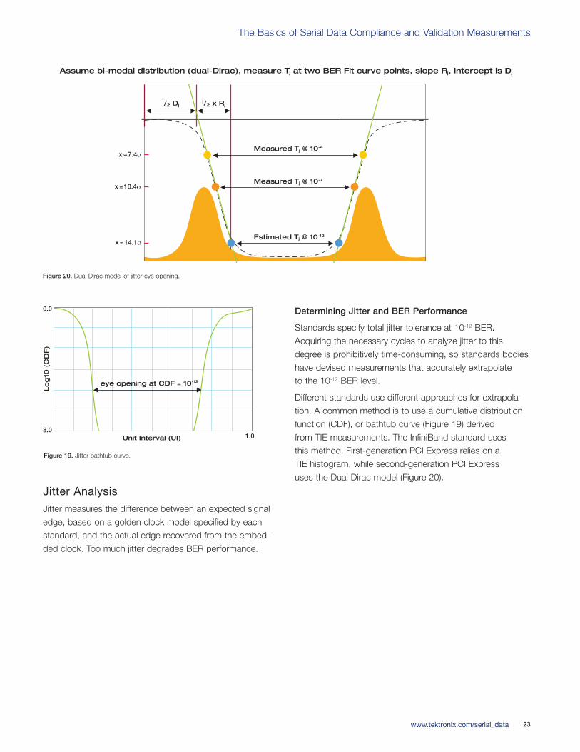
Standards specify total jitter tolerance at 10-12 BER.Acquiring the necessary cycles to analyze jitter to thisdegree is prohibitively time-consuming, so standards bodieshave devised measurements that accurately extrapolate to the 10-12 BER level.
Different standards use different approaches for extrapola-tion. A common method is to use a cumulative distributionfunction (CDF), or bathtub curve (Figure 19) derived from TIE measurements. The InfiniBand standard uses this method. First-generation PCI Express relies on a TIE histogram, while second-generation PCI Express uses the Dual Dirac model (Figure 20).
0.0
1.0
Lo
g10
(C
DF)
8.0 Unit Interval (UI)
eye opening at CDF = 10-12
Figure 19. Jitter bathtub curve.
Figure 20. Dual Dirac model of jitter eye opening.
Assume bi-modal distribution (dual-Dirac), measure Tj at two BER Fit curve points, slope Rj, Intercept is Dj
Measured Tj @ 10-4
Measured Tj @ 10-7
Estimated Tj @ 10-12
x 14.1σ
x 10.4σ
x 7.4σ
1/2 Dj1/2 x Rj
The amount of jitter at 10-12 BER is considered the jitter eye opening, which is different from the eye width of eye measurements. The relationship between Tj, jitter eye opening, and UI is as follows:
Total Jitter + Jitter Eye Opening = 1 Unit Interval
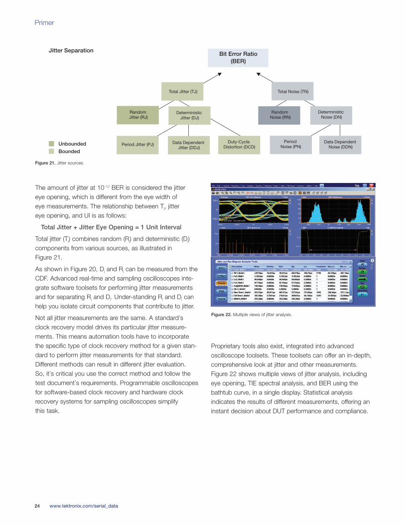
Total jitter (Tj) combines random (Rj) and deterministic (Dj)components from various sources, as illustrated in Figure 21.
As shown in Figure 20, Dj and Rj can be measured from theCDF. Advanced real-time and sampling oscilloscopes inte-grate software toolsets for performing jitter measurementsand for separating Rj and Dj. Under-standing Rj and Dj canhelp you isolate circuit components that contribute to jitter.
Not all jitter measurements are the same. A standard’s clock recovery model drives its particular jitter measure-ments. This means automation tools have to incorporatethe specific type of clock recovery method for a given stan-dard to perform jitter measurements for that standard.Different methods can result in different jitter evaluation. So, it’s critical you use the correct method and follow thetest document’s requirements. Programmable oscilloscopesfor software-based clock recovery and hardware clockrecovery systems for sampling oscilloscopes simplify this task.
Proprietary tools also exist, integrated into advanced oscilloscope toolsets. These toolsets can offer an in-depth,comprehensive look at jitter and other measurements.Figure 22 shows multiple views of jitter analysis, includingeye opening, TIE spectral analysis, and BER using the bathtub curve, in a single display. Statistical analysis indicates the results of different measurements, offering aninstant decision about DUT performance and compliance.
Primer
24 www.tektronix.com/serial_data
Bit Error Ratio(BER)
Jitter Separation
Data Dependent Jitter (DDJ)
Duty-Cycle Distortion (DCD)
Deterministic Jitter (DJ)
Total Jitter (TJ)
Random Jitter (RJ)
Deterministic Noise (DN)
Total Noise (TN)
Random Noise (RN)
Period Jitter (PJ)Data Dependent
Noise (DDN)Period
Noise (PN)Unbounded
Bounded
Figure 22. Multiple views of jitter analysis.
Figure 21. Jitter sources.
The Basics of Serial Data Compliance and Validation Measurements
25www.tektronix.com/serial_data
The more data you can gather about jitter, the better your measurements for this all-important compliance test.Measuring low frequency jitter makes two conflictingdemands on the oscilloscope: asking it to capture tiny timing details and to do so over long spans of time. To accomplish this, the oscilloscope must have both high sampling rates to acquire maximum detail about each cycle, plus a long record length to analyze low-frequency changes over time. Modern oscilloscopeswith up to 50 Gs/s sampling rate and a very deep memoryallow the instrument to capture enough operational cycles to determine the impact of low frequency jitter on the measurements.
Noise Analysis
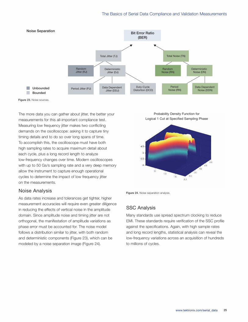
As data rates increase and tolerances get tighter, highermeasurement accuracies will require even greater diligencein reducing the effects of vertical noise in the amplitudedomain. Since amplitude noise and timing jitter are notorthogonal, the manifestation of amplitude variations asphase error must be accounted for. The noise model follows a distribution similar to jitter, with both random and deterministic components (Figure 23), which can bemodeled by a noise separation image (Figure 24).
SSC Analysis
Many standards use spread spectrum clocking to reduceEMI. These standards require verification of the SSC profileagainst the specifications. Again, with high sample ratesand long record lengths, statistical analysis can reveal thelow-frequency variations across an acquisition of hundredsto millions of cycles.
Figure 23. Noise sources.
Figure 24. Noise separation analysis.
Probability Density Function for
Logical 1 Cut at Specified Sampling Phase
Bit Error Ratio(BER)
Noise Separation
Data Dependent Jitter (DDJ)
Duty-Cycle Distortion (DCD)
Deterministic Jitter (DJ)
Total Jitter (TJ)
Random Jitter (RJ)
Deterministic Noise (DN)
Total Noise (TN)
Random Noise (RN)
Period Jitter (PJ)Data Dependent
Noise (DDN)Period
Noise (RN)Unbounded
Bounded
Primer
26 www.tektronix.com/serial_data
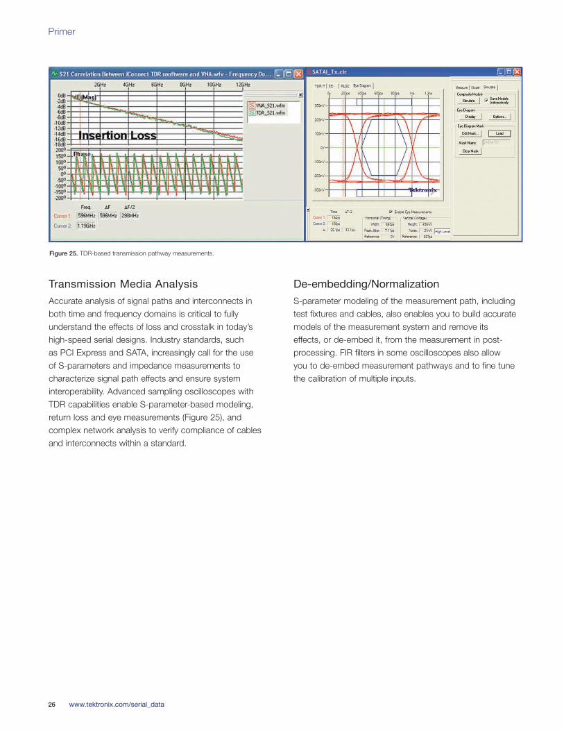
Transmission Media Analysis
Accurate analysis of signal paths and interconnects in both time and frequency domains is critical to fully understand the effects of loss and crosstalk in today’s high-speed serial designs. Industry standards, such as PCI Express and SATA, increasingly call for the use of S-parameters and impedance measurements to characterize signal path effects and ensure system interoperability. Advanced sampling oscilloscopes with TDR capabilities enable S-parameter-based modeling,return loss and eye measurements (Figure 25), and complex network analysis to verify compliance of cablesand interconnects within a standard.
De-embedding/Normalization
S-parameter modeling of the measurement path, including test fixtures and cables, also enables you to build accuratemodels of the measurement system and remove its effects, or de-embed it, from the measurement in post-processing. FIR filters in some oscilloscopes also allow you to de-embed measurement pathways and to fine tunethe calibration of multiple inputs.
Figure 25. TDR-based transmission pathway measurements.
The Basics of Serial Data Compliance and Validation Measurements
27www.tektronix.com/serial_data
SummaryPhysical compliance verification for next-generation high-speed serial standards is more complex and demanding ofthe test equipment, connectivity methods, and analysistools than with previous generation standards. Transmissionmedia plays a greater role in signal integrity, and more focuson media and receiver testing are common in Gen 2 andGen 3 compliance requirements. Higher bit rates, shorterUI, and tighter tolerances require you to take a new look atyour testing strategy, including fixtures and equipment, for physical testing.
A generation of measurement tools has followed the evolution of serial architectures, giving you better tools for accelerated testing and to help you with serial measurement and compliance challenges. These solutionsdeliver the performance and technologies to capture, display, and analyze the most complex serial signals at the highest data rates.
Further ReadingTektronix offers many more application notes and primerson specific topics for a much closer look at serial standards,how to test to them, and what equipment to use. Pleasevisit www.tektronix.com for more information.
For Further InformationTektronix maintains a comprehensive, constantly expandingcollection of application notes, technical briefs and otherresources to help engineers working on the cutting edge oftechnology. Please visit www.tektronix.com
Copyright © 2010, Tektronix. All rights reserved. Tektronix products are coveredby U.S. and foreign patents, issued and pending. Information in this publicationsupersedes that in all previously published material. Specification and pricechange privileges reserved. TEKTRONIX and TEK are registered trademarks of Tektronix, Inc. All other trade names referenced are the service marks, trademarks or registered trademarks of their respective companies. 03/10 EA/ 55W-16736-3
Contact Tektronix:ASEAN / Australasia (65) 6356 3900
Austria 00800 2255 4835*
Balkans, Israel, South Africa and other ISE Countries +41 52 675 3777
Belgium 00800 2255 4835*
Brazil +55 (11) 3759 7600
Canada 1 (800) 833-9200
Central East Europe, Ukraine and the Baltics +41 52 675 3777
Central Europe & Greece +41 52 675 3777
Denmark +45 80 88 1401
Finland +41 52 675 3777
France 00800 2255 4835*
Germany 00800 2255 4835*
Hong Kong 400-820-5835
India (91) 80-42922600
Italy 00800 2255 4835*
Japan 81 (3) 6714-3010
Luxembourg +41 52 675 3777
Mexico, Central/South America & Caribbean 52 (55) 53 35 10 85
Middle East, Asia and North Africa +41 52 675 3777
The Netherlands 00800 2255 4835*
Norway 800 16098
People’s Republic of China 400-820-5835
Poland +41 52 675 3777
Portugal 80 08 12370
Republic of Korea 82 (2) 6917-5000
Russia & CIS +7 (495) 7484900
South Africa +27 11 206 8360
Spain 00800 2255 4835*
Sweden 00800 2255 4835*
Switzerland 00800 2255 4835*
Taiwan 886 (2) 2722-9622
United Kingdom & Ireland 00800 2255 4835*
USA 1 (800) 833-9200
** EEuurrooppeeaann ttoollll--ffrreeee nnuummbbeerr.. IIff nnoott aacccceessssiibbllee,, ccaallll:: ++4411 5522 667755 33777777
Contact List Updated 09 December 2009